US6342434B1 - Methods of processing semiconductor wafer, and producing IC card, and carrier - Google Patents
Methods of processing semiconductor wafer, and producing IC card, and carrierDownload PDFInfo
- Publication number
- US6342434B1 US6342434B1US09/077,548US7754898AUS6342434B1US 6342434 B1US6342434 B1US 6342434B1US 7754898 AUS7754898 AUS 7754898AUS 6342434 B1US6342434 B1US 6342434B1
- Authority
- US
- United States
- Prior art keywords
- semiconductor wafer
- carrier
- wafer
- base
- composite
- Prior art date
- Legal status (The legal status is an assumption and is not a legal conclusion. Google has not performed a legal analysis and makes no representation as to the accuracy of the status listed.)
- Expired - Lifetime
Links
Images


Classifications
- H—ELECTRICITY
- H01—ELECTRIC ELEMENTS
- H01L—SEMICONDUCTOR DEVICES NOT COVERED BY CLASS H10
- H01L21/00—Processes or apparatus adapted for the manufacture or treatment of semiconductor or solid state devices or of parts thereof
- H01L21/02—Manufacture or treatment of semiconductor devices or of parts thereof
- H01L21/04—Manufacture or treatment of semiconductor devices or of parts thereof the devices having potential barriers, e.g. a PN junction, depletion layer or carrier concentration layer
- H01L21/18—Manufacture or treatment of semiconductor devices or of parts thereof the devices having potential barriers, e.g. a PN junction, depletion layer or carrier concentration layer the devices having semiconductor bodies comprising elements of Group IV of the Periodic Table or AIIIBV compounds with or without impurities, e.g. doping materials
- H01L21/30—Treatment of semiconductor bodies using processes or apparatus not provided for in groups H01L21/20 - H01L21/26
- H01L21/302—Treatment of semiconductor bodies using processes or apparatus not provided for in groups H01L21/20 - H01L21/26 to change their surface-physical characteristics or shape, e.g. etching, polishing, cutting
- H01L21/306—Chemical or electrical treatment, e.g. electrolytic etching
- H—ELECTRICITY
- H01—ELECTRIC ELEMENTS
- H01L—SEMICONDUCTOR DEVICES NOT COVERED BY CLASS H10
- H01L21/00—Processes or apparatus adapted for the manufacture or treatment of semiconductor or solid state devices or of parts thereof
- H01L21/67—Apparatus specially adapted for handling semiconductor or electric solid state devices during manufacture or treatment thereof; Apparatus specially adapted for handling wafers during manufacture or treatment of semiconductor or electric solid state devices or components ; Apparatus not specifically provided for elsewhere
- H01L21/683—Apparatus specially adapted for handling semiconductor or electric solid state devices during manufacture or treatment thereof; Apparatus specially adapted for handling wafers during manufacture or treatment of semiconductor or electric solid state devices or components ; Apparatus not specifically provided for elsewhere for supporting or gripping
- H01L21/6835—Apparatus specially adapted for handling semiconductor or electric solid state devices during manufacture or treatment thereof; Apparatus specially adapted for handling wafers during manufacture or treatment of semiconductor or electric solid state devices or components ; Apparatus not specifically provided for elsewhere for supporting or gripping using temporarily an auxiliary support
- G—PHYSICS
- G06—COMPUTING OR CALCULATING; COUNTING
- G06K—GRAPHICAL DATA READING; PRESENTATION OF DATA; RECORD CARRIERS; HANDLING RECORD CARRIERS
- G06K19/00—Record carriers for use with machines and with at least a part designed to carry digital markings
- G06K19/06—Record carriers for use with machines and with at least a part designed to carry digital markings characterised by the kind of the digital marking, e.g. shape, nature, code
- G06K19/067—Record carriers with conductive marks, printed circuits or semiconductor circuit elements, e.g. credit or identity cards also with resonating or responding marks without active components
- G06K19/07—Record carriers with conductive marks, printed circuits or semiconductor circuit elements, e.g. credit or identity cards also with resonating or responding marks without active components with integrated circuit chips
- G06K19/077—Constructional details, e.g. mounting of circuits in the carrier
- G06K19/07749—Constructional details, e.g. mounting of circuits in the carrier the record carrier being capable of non-contact communication, e.g. constructional details of the antenna of a non-contact smart card
- G06K19/0775—Constructional details, e.g. mounting of circuits in the carrier the record carrier being capable of non-contact communication, e.g. constructional details of the antenna of a non-contact smart card arrangements for connecting the integrated circuit to the antenna
- G—PHYSICS
- G06—COMPUTING OR CALCULATING; COUNTING
- G06K—GRAPHICAL DATA READING; PRESENTATION OF DATA; RECORD CARRIERS; HANDLING RECORD CARRIERS
- G06K19/00—Record carriers for use with machines and with at least a part designed to carry digital markings
- G06K19/06—Record carriers for use with machines and with at least a part designed to carry digital markings characterised by the kind of the digital marking, e.g. shape, nature, code
- G06K19/067—Record carriers with conductive marks, printed circuits or semiconductor circuit elements, e.g. credit or identity cards also with resonating or responding marks without active components
- G06K19/07—Record carriers with conductive marks, printed circuits or semiconductor circuit elements, e.g. credit or identity cards also with resonating or responding marks without active components with integrated circuit chips
- G06K19/077—Constructional details, e.g. mounting of circuits in the carrier
- G06K19/07749—Constructional details, e.g. mounting of circuits in the carrier the record carrier being capable of non-contact communication, e.g. constructional details of the antenna of a non-contact smart card
- G06K19/07773—Antenna details
- G06K19/07777—Antenna details the antenna being of the inductive type
- G06K19/07779—Antenna details the antenna being of the inductive type the inductive antenna being a coil
- G06K19/07783—Antenna details the antenna being of the inductive type the inductive antenna being a coil the coil being planar
- H—ELECTRICITY
- H01—ELECTRIC ELEMENTS
- H01L—SEMICONDUCTOR DEVICES NOT COVERED BY CLASS H10
- H01L23/00—Details of semiconductor or other solid state devices
- H01L23/48—Arrangements for conducting electric current to or from the solid state body in operation, e.g. leads, terminal arrangements ; Selection of materials therefor
- H01L23/488—Arrangements for conducting electric current to or from the solid state body in operation, e.g. leads, terminal arrangements ; Selection of materials therefor consisting of soldered or bonded constructions
- H01L23/498—Leads, i.e. metallisations or lead-frames on insulating substrates, e.g. chip carriers
- H01L23/49855—Leads, i.e. metallisations or lead-frames on insulating substrates, e.g. chip carriers for flat-cards, e.g. credit cards
- H—ELECTRICITY
- H01—ELECTRIC ELEMENTS
- H01L—SEMICONDUCTOR DEVICES NOT COVERED BY CLASS H10
- H01L23/00—Details of semiconductor or other solid state devices
- H01L23/52—Arrangements for conducting electric current within the device in operation from one component to another, i.e. interconnections, e.g. wires, lead frames
- H01L23/538—Arrangements for conducting electric current within the device in operation from one component to another, i.e. interconnections, e.g. wires, lead frames the interconnection structure between a plurality of semiconductor chips being formed on, or in, insulating substrates
- H01L23/5388—Arrangements for conducting electric current within the device in operation from one component to another, i.e. interconnections, e.g. wires, lead frames the interconnection structure between a plurality of semiconductor chips being formed on, or in, insulating substrates for flat cards, e.g. credit cards
- H—ELECTRICITY
- H01—ELECTRIC ELEMENTS
- H01L—SEMICONDUCTOR DEVICES NOT COVERED BY CLASS H10
- H01L24/00—Arrangements for connecting or disconnecting semiconductor or solid-state bodies; Methods or apparatus related thereto
- H01L24/01—Means for bonding being attached to, or being formed on, the surface to be connected, e.g. chip-to-package, die-attach, "first-level" interconnects; Manufacturing methods related thereto
- H01L24/26—Layer connectors, e.g. plate connectors, solder or adhesive layers; Manufacturing methods related thereto
- H01L24/27—Manufacturing methods
- H—ELECTRICITY
- H01—ELECTRIC ELEMENTS
- H01L—SEMICONDUCTOR DEVICES NOT COVERED BY CLASS H10
- H01L24/00—Arrangements for connecting or disconnecting semiconductor or solid-state bodies; Methods or apparatus related thereto
- H01L24/01—Means for bonding being attached to, or being formed on, the surface to be connected, e.g. chip-to-package, die-attach, "first-level" interconnects; Manufacturing methods related thereto
- H01L24/26—Layer connectors, e.g. plate connectors, solder or adhesive layers; Manufacturing methods related thereto
- H01L24/28—Structure, shape, material or disposition of the layer connectors prior to the connecting process
- H—ELECTRICITY
- H01—ELECTRIC ELEMENTS
- H01L—SEMICONDUCTOR DEVICES NOT COVERED BY CLASS H10
- H01L24/00—Arrangements for connecting or disconnecting semiconductor or solid-state bodies; Methods or apparatus related thereto
- H01L24/80—Methods for connecting semiconductor or other solid state bodies using means for bonding being attached to, or being formed on, the surface to be connected
- H01L24/83—Methods for connecting semiconductor or other solid state bodies using means for bonding being attached to, or being formed on, the surface to be connected using a layer connector
- H—ELECTRICITY
- H01—ELECTRIC ELEMENTS
- H01L—SEMICONDUCTOR DEVICES NOT COVERED BY CLASS H10
- H01L2221/00—Processes or apparatus adapted for the manufacture or treatment of semiconductor or solid state devices or of parts thereof covered by H01L21/00
- H01L2221/67—Apparatus for handling semiconductor or electric solid state devices during manufacture or treatment thereof; Apparatus for handling wafers during manufacture or treatment of semiconductor or electric solid state devices or components; Apparatus not specifically provided for elsewhere
- H01L2221/683—Apparatus for handling semiconductor or electric solid state devices during manufacture or treatment thereof; Apparatus for handling wafers during manufacture or treatment of semiconductor or electric solid state devices or components; Apparatus not specifically provided for elsewhere for supporting or gripping
- H01L2221/68304—Apparatus for handling semiconductor or electric solid state devices during manufacture or treatment thereof; Apparatus for handling wafers during manufacture or treatment of semiconductor or electric solid state devices or components; Apparatus not specifically provided for elsewhere for supporting or gripping using temporarily an auxiliary support
- H01L2221/68318—Auxiliary support including means facilitating the separation of a device or wafer from the auxiliary support
- H—ELECTRICITY
- H01—ELECTRIC ELEMENTS
- H01L—SEMICONDUCTOR DEVICES NOT COVERED BY CLASS H10
- H01L2224/00—Indexing scheme for arrangements for connecting or disconnecting semiconductor or solid-state bodies and methods related thereto as covered by H01L24/00
- H01L2224/01—Means for bonding being attached to, or being formed on, the surface to be connected, e.g. chip-to-package, die-attach, "first-level" interconnects; Manufacturing methods related thereto
- H01L2224/02—Bonding areas; Manufacturing methods related thereto
- H01L2224/04—Structure, shape, material or disposition of the bonding areas prior to the connecting process
- H01L2224/05—Structure, shape, material or disposition of the bonding areas prior to the connecting process of an individual bonding area
- H01L2224/05001—Internal layers
- H01L2224/0502—Disposition
- H01L2224/05022—Disposition the internal layer being at least partially embedded in the surface
- H—ELECTRICITY
- H01—ELECTRIC ELEMENTS
- H01L—SEMICONDUCTOR DEVICES NOT COVERED BY CLASS H10
- H01L2224/00—Indexing scheme for arrangements for connecting or disconnecting semiconductor or solid-state bodies and methods related thereto as covered by H01L24/00
- H01L2224/01—Means for bonding being attached to, or being formed on, the surface to be connected, e.g. chip-to-package, die-attach, "first-level" interconnects; Manufacturing methods related thereto
- H01L2224/02—Bonding areas; Manufacturing methods related thereto
- H01L2224/04—Structure, shape, material or disposition of the bonding areas prior to the connecting process
- H01L2224/05—Structure, shape, material or disposition of the bonding areas prior to the connecting process of an individual bonding area
- H01L2224/0554—External layer
- H01L2224/0556—Disposition
- H01L2224/05571—Disposition the external layer being disposed in a recess of the surface
- H01L2224/05572—Disposition the external layer being disposed in a recess of the surface the external layer extending out of an opening
- H—ELECTRICITY
- H01—ELECTRIC ELEMENTS
- H01L—SEMICONDUCTOR DEVICES NOT COVERED BY CLASS H10
- H01L2224/00—Indexing scheme for arrangements for connecting or disconnecting semiconductor or solid-state bodies and methods related thereto as covered by H01L24/00
- H01L2224/01—Means for bonding being attached to, or being formed on, the surface to be connected, e.g. chip-to-package, die-attach, "first-level" interconnects; Manufacturing methods related thereto
- H01L2224/10—Bump connectors; Manufacturing methods related thereto
- H01L2224/15—Structure, shape, material or disposition of the bump connectors after the connecting process
- H01L2224/16—Structure, shape, material or disposition of the bump connectors after the connecting process of an individual bump connector
- H01L2224/161—Disposition
- H01L2224/16151—Disposition the bump connector connecting between a semiconductor or solid-state body and an item not being a semiconductor or solid-state body, e.g. chip-to-substrate, chip-to-passive
- H01L2224/16221—Disposition the bump connector connecting between a semiconductor or solid-state body and an item not being a semiconductor or solid-state body, e.g. chip-to-substrate, chip-to-passive the body and the item being stacked
- H01L2224/16225—Disposition the bump connector connecting between a semiconductor or solid-state body and an item not being a semiconductor or solid-state body, e.g. chip-to-substrate, chip-to-passive the body and the item being stacked the item being non-metallic, e.g. insulating substrate with or without metallisation
- H01L2224/16227—Disposition the bump connector connecting between a semiconductor or solid-state body and an item not being a semiconductor or solid-state body, e.g. chip-to-substrate, chip-to-passive the body and the item being stacked the item being non-metallic, e.g. insulating substrate with or without metallisation the bump connector connecting to a bond pad of the item
- H—ELECTRICITY
- H01—ELECTRIC ELEMENTS
- H01L—SEMICONDUCTOR DEVICES NOT COVERED BY CLASS H10
- H01L2224/00—Indexing scheme for arrangements for connecting or disconnecting semiconductor or solid-state bodies and methods related thereto as covered by H01L24/00
- H01L2224/01—Means for bonding being attached to, or being formed on, the surface to be connected, e.g. chip-to-package, die-attach, "first-level" interconnects; Manufacturing methods related thereto
- H01L2224/26—Layer connectors, e.g. plate connectors, solder or adhesive layers; Manufacturing methods related thereto
- H01L2224/28—Structure, shape, material or disposition of the layer connectors prior to the connecting process
- H01L2224/29—Structure, shape, material or disposition of the layer connectors prior to the connecting process of an individual layer connector
- H01L2224/29001—Core members of the layer connector
- H01L2224/29099—Material
- H01L2224/2919—Material with a principal constituent of the material being a polymer, e.g. polyester, phenolic based polymer, epoxy
- H—ELECTRICITY
- H01—ELECTRIC ELEMENTS
- H01L—SEMICONDUCTOR DEVICES NOT COVERED BY CLASS H10
- H01L2224/00—Indexing scheme for arrangements for connecting or disconnecting semiconductor or solid-state bodies and methods related thereto as covered by H01L24/00
- H01L2224/80—Methods for connecting semiconductor or other solid state bodies using means for bonding being attached to, or being formed on, the surface to be connected
- H01L2224/81—Methods for connecting semiconductor or other solid state bodies using means for bonding being attached to, or being formed on, the surface to be connected using a bump connector
- H01L2224/819—Methods for connecting semiconductor or other solid state bodies using means for bonding being attached to, or being formed on, the surface to be connected using a bump connector with the bump connector not providing any mechanical bonding
- H01L2224/81901—Pressing the bump connector against the bonding areas by means of another connector
- H01L2224/81903—Pressing the bump connector against the bonding areas by means of another connector by means of a layer connector
- H—ELECTRICITY
- H01—ELECTRIC ELEMENTS
- H01L—SEMICONDUCTOR DEVICES NOT COVERED BY CLASS H10
- H01L2224/00—Indexing scheme for arrangements for connecting or disconnecting semiconductor or solid-state bodies and methods related thereto as covered by H01L24/00
- H01L2224/80—Methods for connecting semiconductor or other solid state bodies using means for bonding being attached to, or being formed on, the surface to be connected
- H01L2224/83—Methods for connecting semiconductor or other solid state bodies using means for bonding being attached to, or being formed on, the surface to be connected using a layer connector
- H01L2224/8319—Arrangement of the layer connectors prior to mounting
- H—ELECTRICITY
- H01—ELECTRIC ELEMENTS
- H01L—SEMICONDUCTOR DEVICES NOT COVERED BY CLASS H10
- H01L2224/00—Indexing scheme for arrangements for connecting or disconnecting semiconductor or solid-state bodies and methods related thereto as covered by H01L24/00
- H01L2224/80—Methods for connecting semiconductor or other solid state bodies using means for bonding being attached to, or being formed on, the surface to be connected
- H01L2224/83—Methods for connecting semiconductor or other solid state bodies using means for bonding being attached to, or being formed on, the surface to be connected using a layer connector
- H01L2224/838—Bonding techniques
- H01L2224/8385—Bonding techniques using a polymer adhesive, e.g. an adhesive based on silicone, epoxy, polyimide, polyester
- H01L2224/83851—Bonding techniques using a polymer adhesive, e.g. an adhesive based on silicone, epoxy, polyimide, polyester being an anisotropic conductive adhesive
- H—ELECTRICITY
- H01—ELECTRIC ELEMENTS
- H01L—SEMICONDUCTOR DEVICES NOT COVERED BY CLASS H10
- H01L2924/00—Indexing scheme for arrangements or methods for connecting or disconnecting semiconductor or solid-state bodies as covered by H01L24/00
- H01L2924/01—Chemical elements
- H01L2924/01005—Boron [B]
- H—ELECTRICITY
- H01—ELECTRIC ELEMENTS
- H01L—SEMICONDUCTOR DEVICES NOT COVERED BY CLASS H10
- H01L2924/00—Indexing scheme for arrangements or methods for connecting or disconnecting semiconductor or solid-state bodies as covered by H01L24/00
- H01L2924/01—Chemical elements
- H01L2924/01006—Carbon [C]
- H—ELECTRICITY
- H01—ELECTRIC ELEMENTS
- H01L—SEMICONDUCTOR DEVICES NOT COVERED BY CLASS H10
- H01L2924/00—Indexing scheme for arrangements or methods for connecting or disconnecting semiconductor or solid-state bodies as covered by H01L24/00
- H01L2924/01—Chemical elements
- H01L2924/01013—Aluminum [Al]
- H—ELECTRICITY
- H01—ELECTRIC ELEMENTS
- H01L—SEMICONDUCTOR DEVICES NOT COVERED BY CLASS H10
- H01L2924/00—Indexing scheme for arrangements or methods for connecting or disconnecting semiconductor or solid-state bodies as covered by H01L24/00
- H01L2924/01—Chemical elements
- H01L2924/01015—Phosphorus [P]
- H—ELECTRICITY
- H01—ELECTRIC ELEMENTS
- H01L—SEMICONDUCTOR DEVICES NOT COVERED BY CLASS H10
- H01L2924/00—Indexing scheme for arrangements or methods for connecting or disconnecting semiconductor or solid-state bodies as covered by H01L24/00
- H01L2924/01—Chemical elements
- H01L2924/01024—Chromium [Cr]
- H—ELECTRICITY
- H01—ELECTRIC ELEMENTS
- H01L—SEMICONDUCTOR DEVICES NOT COVERED BY CLASS H10
- H01L2924/00—Indexing scheme for arrangements or methods for connecting or disconnecting semiconductor or solid-state bodies as covered by H01L24/00
- H01L2924/01—Chemical elements
- H01L2924/01027—Cobalt [Co]
- H—ELECTRICITY
- H01—ELECTRIC ELEMENTS
- H01L—SEMICONDUCTOR DEVICES NOT COVERED BY CLASS H10
- H01L2924/00—Indexing scheme for arrangements or methods for connecting or disconnecting semiconductor or solid-state bodies as covered by H01L24/00
- H01L2924/01—Chemical elements
- H01L2924/01029—Copper [Cu]
- H—ELECTRICITY
- H01—ELECTRIC ELEMENTS
- H01L—SEMICONDUCTOR DEVICES NOT COVERED BY CLASS H10
- H01L2924/00—Indexing scheme for arrangements or methods for connecting or disconnecting semiconductor or solid-state bodies as covered by H01L24/00
- H01L2924/01—Chemical elements
- H01L2924/01033—Arsenic [As]
- H—ELECTRICITY
- H01—ELECTRIC ELEMENTS
- H01L—SEMICONDUCTOR DEVICES NOT COVERED BY CLASS H10
- H01L2924/00—Indexing scheme for arrangements or methods for connecting or disconnecting semiconductor or solid-state bodies as covered by H01L24/00
- H01L2924/01—Chemical elements
- H01L2924/01046—Palladium [Pd]
- H—ELECTRICITY
- H01—ELECTRIC ELEMENTS
- H01L—SEMICONDUCTOR DEVICES NOT COVERED BY CLASS H10
- H01L2924/00—Indexing scheme for arrangements or methods for connecting or disconnecting semiconductor or solid-state bodies as covered by H01L24/00
- H01L2924/01—Chemical elements
- H01L2924/0105—Tin [Sn]
- H—ELECTRICITY
- H01—ELECTRIC ELEMENTS
- H01L—SEMICONDUCTOR DEVICES NOT COVERED BY CLASS H10
- H01L2924/00—Indexing scheme for arrangements or methods for connecting or disconnecting semiconductor or solid-state bodies as covered by H01L24/00
- H01L2924/01—Chemical elements
- H01L2924/01057—Lanthanum [La]
- H—ELECTRICITY
- H01—ELECTRIC ELEMENTS
- H01L—SEMICONDUCTOR DEVICES NOT COVERED BY CLASS H10
- H01L2924/00—Indexing scheme for arrangements or methods for connecting or disconnecting semiconductor or solid-state bodies as covered by H01L24/00
- H01L2924/01—Chemical elements
- H01L2924/01074—Tungsten [W]
- H—ELECTRICITY
- H01—ELECTRIC ELEMENTS
- H01L—SEMICONDUCTOR DEVICES NOT COVERED BY CLASS H10
- H01L2924/00—Indexing scheme for arrangements or methods for connecting or disconnecting semiconductor or solid-state bodies as covered by H01L24/00
- H01L2924/01—Chemical elements
- H01L2924/01078—Platinum [Pt]
- H—ELECTRICITY
- H01—ELECTRIC ELEMENTS
- H01L—SEMICONDUCTOR DEVICES NOT COVERED BY CLASS H10
- H01L2924/00—Indexing scheme for arrangements or methods for connecting or disconnecting semiconductor or solid-state bodies as covered by H01L24/00
- H01L2924/01—Chemical elements
- H01L2924/01079—Gold [Au]
- H—ELECTRICITY
- H01—ELECTRIC ELEMENTS
- H01L—SEMICONDUCTOR DEVICES NOT COVERED BY CLASS H10
- H01L2924/00—Indexing scheme for arrangements or methods for connecting or disconnecting semiconductor or solid-state bodies as covered by H01L24/00
- H01L2924/01—Chemical elements
- H01L2924/01082—Lead [Pb]
- H—ELECTRICITY
- H01—ELECTRIC ELEMENTS
- H01L—SEMICONDUCTOR DEVICES NOT COVERED BY CLASS H10
- H01L2924/00—Indexing scheme for arrangements or methods for connecting or disconnecting semiconductor or solid-state bodies as covered by H01L24/00
- H01L2924/013—Alloys
- H01L2924/0132—Binary Alloys
- H—ELECTRICITY
- H01—ELECTRIC ELEMENTS
- H01L—SEMICONDUCTOR DEVICES NOT COVERED BY CLASS H10
- H01L2924/00—Indexing scheme for arrangements or methods for connecting or disconnecting semiconductor or solid-state bodies as covered by H01L24/00
- H01L2924/06—Polymers
- H01L2924/0665—Epoxy resin
- H—ELECTRICITY
- H01—ELECTRIC ELEMENTS
- H01L—SEMICONDUCTOR DEVICES NOT COVERED BY CLASS H10
- H01L2924/00—Indexing scheme for arrangements or methods for connecting or disconnecting semiconductor or solid-state bodies as covered by H01L24/00
- H01L2924/06—Polymers
- H01L2924/078—Adhesive characteristics other than chemical
- H01L2924/0781—Adhesive characteristics other than chemical being an ohmic electrical conductor
- H01L2924/07811—Extrinsic, i.e. with electrical conductive fillers
- H—ELECTRICITY
- H01—ELECTRIC ELEMENTS
- H01L—SEMICONDUCTOR DEVICES NOT COVERED BY CLASS H10
- H01L2924/00—Indexing scheme for arrangements or methods for connecting or disconnecting semiconductor or solid-state bodies as covered by H01L24/00
- H01L2924/10—Details of semiconductor or other solid state devices to be connected
- H01L2924/11—Device type
- H01L2924/14—Integrated circuits
- H—ELECTRICITY
- H01—ELECTRIC ELEMENTS
- H01L—SEMICONDUCTOR DEVICES NOT COVERED BY CLASS H10
- H01L2924/00—Indexing scheme for arrangements or methods for connecting or disconnecting semiconductor or solid-state bodies as covered by H01L24/00
- H01L2924/19—Details of hybrid assemblies other than the semiconductor or other solid state devices to be connected
- H01L2924/1901—Structure
- H01L2924/1904—Component type
- H01L2924/19041—Component type being a capacitor
- H—ELECTRICITY
- H01—ELECTRIC ELEMENTS
- H01L—SEMICONDUCTOR DEVICES NOT COVERED BY CLASS H10
- H01L2924/00—Indexing scheme for arrangements or methods for connecting or disconnecting semiconductor or solid-state bodies as covered by H01L24/00
- H01L2924/30—Technical effects
- H01L2924/301—Electrical effects
- H01L2924/3025—Electromagnetic shielding
- H—ELECTRICITY
- H01—ELECTRIC ELEMENTS
- H01L—SEMICONDUCTOR DEVICES NOT COVERED BY CLASS H10
- H01L2924/00—Indexing scheme for arrangements or methods for connecting or disconnecting semiconductor or solid-state bodies as covered by H01L24/00
- H01L2924/30—Technical effects
- H01L2924/35—Mechanical effects
- H01L2924/351—Thermal stress
- H01L2924/3511—Warping
Definitions
- the present inventionrelates to semiconductor wafer processing techniques, and particularly to a technique effective for use in handling semiconductor wafers when the semiconductor wafers are processed to a very small thickness of 100 ⁇ m or below.
- grindingis a technique for grinding rear surface of a semiconductor wafer with a diamond grindstone
- a etchingis the technique for etching the rear surface of a semiconductor wafer with a mixture of chiefly fluoric acid and nitric acid while the semiconductor wafer is being rotated with high speed
- lappingis a technique for grinding the rear surface of a semiconductor wafer with abrasive grains.
- the thinning process by the grinding or lappingis able to grind semiconductor wafers of general thickness, or about 625 ⁇ m (or 725 ⁇ m) to a thickness of about 300 ⁇ m, but has a difficulty when trying to grind to a thickness of, for example, 100 ⁇ m or below because the semiconductor wafer might be cracked even under strict care when removing it from the grinder. Even if the wafer is not cracked, it is remarkably warped depending on the stress in the passivation film on the wafer surface and the internal stress of the wafer. This warp causes operational problems in the following processes such as dicing. In addition, it is difficult to process large-diameter semiconductor wafers, or 12-inch or above wafers to a specified level of flatness and uniformity.
- the inventorshave found to fix the semiconductor wafer to a certain support base with tape and process it after various examinations.
- normal tapeis also discarded after use in the process of each wafer, thus increasing the cost, or causing a new problem.
- the semiconductor wafer processing methodincludes a first step of preparing a plate-like or film-shaped carrier that is formed of a base and an adhesive member provided on one surface of the base, a second step of producing a wafer composite by bonding a semiconductor wafer to the carrier in such a manner that the rear surface of the wafer with no circuit elements formed therein is opposite to the carrier, and a third step of making the semiconductor wafer thin by spin-coating an etchant on the rear surface of the semiconductor wafer of the wafer composite that is supported with its semiconductor wafer side up.
- the semiconductor wafer of the wafer compositeis made to have a larger diameter than the carrier so that all the outer peripheral edge of the semiconductor wafer overhangs from the carrier when the wafer composite is formed by bonding the wafer on the carrier.
- the semiconductor wafercan be thinned while a gas is being blown from below against the wafer composite.
- the semiconductor wafermay be made to have a diameter equal to or smaller than the carrier so that the peripheral edge of the wafer does not overhang from the carrier when the wafer composite is formed.
- a fourth step and a fifth stepmay be provided.
- the fourth stepis for sticking the rear side of the wafer on a dicing sheet and peeling off the carrier
- the fifth stepis for dicing the semiconductor wafer on the dicing sheet into individual semiconductor chips.
- the semiconductor wafer processing method of the inventionincludes a first step of preparing a semiconductor wafer with a passivation film formed on its main surface in which circuit elements are already built, a second step of preparing a plate-like or film-like carrier that is formed of a base and an adhesive member provided on one surface of the base, a third step of producing a wafer composite by bonding the semiconductor wafer to the carrier in such a manner that the rear surface of the wafer with no circuit elements formed therein is opposite to the carrier, and a fourth step of holding the wafer composite with its semiconductor wafer side up and spin-coating an etchant on the rear surface of the semiconductor wafer thereby to thin the semiconductor wafer.
- the IC card producing methodincludes a first step of preparing a plate-like or film-like carrier that is formed of a base and an adhesive member provided on one side of the base, a second step of producing a wafer composite by bonding a semiconductor wafer to the carrier in such a manner that the rear surface of the wafer with no circuit elements formed therein is opposite to the carrier, a third step of holding the wafer composite with its semiconductor wafer side up and spin-coating an etchant on the rear surface of the semiconductor wafer thereby to thin the semiconductor wafer, a fourth step of attaching the thinned rear surface of the semiconductor wafer to a dicing sheet and peeling off the carrier from the wafer composite, a fifth step of dicing the semiconductor wafer left on the dicing sheet into individual semiconductor chips, a sixth step of reducing or loosing or losing the adhesion of the dicing sheet, a seventh step of mounting one or ones of the semiconductor chips on a card substrate at chip-mounting positions, and an eighth step
- an IC card producing methodincluding a first step of preparing a semiconductor wafer with a passivation film formed on its main surface in which circuit elements are already built, a second step of preparing a plate-like or film-like carrier that is formed of a base and an adhesive member provided on one surface of the base, a third step of producing a wafer composite by bonding a semiconductor wafer to the carrier in such a manner that the rear surface of the wafer with no circuit elements formed therein is opposite to the carrier, a fourth step of holding the wafer composite with its semiconductor wafer side up and spin-coating an etchant on the rear surface of the semiconductor wafer thereby to thin the semiconductor wafer, a fifth step of attaching the thinned rear side of the semiconductor wafer to a dicing sheet and peeling off the carrier from the wafer composite, a sixth step of dicing the semiconductor wafer left on the dicing sheet into individual semiconductor chips, a seventh step of reducing or loosing or losing the adhesion
- the thickness of the adhesive member provided on the baseshould be equal to or larger than the height of the bumps.
- the carrier in the inventionis used in the semiconductor wafer processing method, and its adhesive member comprises an elastically flexible suction pad for sucking the semiconductor wafer by vacuum.
- the suction,padmay have a size large enough to suck substantially an entire surface of the semiconductor wafer.
- itmay be formed in a ring shape along the outer periphery of the semiconductor wafer.
- a plurality of such suction padsmay be provided over an entire surface of the base in order to hold the semiconductor wafer at a plurality of locations.
- the carrier in the inventionis used in the semiconductor wafer processing method, and its adhesive member comprises a suction groove that is formed in the base to be communicated with a vacuum hole connected to a vacuum pump so that the semiconductor wafer is sucked by vacuum and peeled off from the carrier by restoring to atmospheric pressure.
- the carrier in the inventionis used in the semiconductor wafer processing method according to the invention, and its adhesive member is constituted by a plurality of suction holes which are formed in one surface of the base at different locations to be communicated with a vacuum hole connected to a vacuum pump so that the semiconductor wafer is sucked by negative pressure and peeled off from the carrier by restoring to atmospheric pressure.
- the carrier in the inventionis used in the semiconductor wafer processing method according to the invention, and its adhesive member comprises a porous member that has a great number of small holes and is provided on one surface of the base for the small holes to be communicated with a vacuum hole connected to a vacuum pump so that the semiconductor wafer is sucked by vacuum and that it is peeled off from the carrier by restoring to atmospheric pressure.
- the carrier in the inventionis used in the semiconductor wafer processing method according to the invention, and its adhesive member includes an exfoliation portion coplanar with the base to form a plurality of small recesses, and gelled silicone interposed between the peeling portion and the semiconductor wafer to make the base adhere to the semiconductor wafer, whereby when the surroundings of the exfoliation portion are evacuated the silicone is sunk in the recesses so as to be peeled off from the semiconductor wafer.
- the exfoliation portion of the carriermay be a net or an irregular surface formed on the base.
- the carrier employed in the semiconductor wafer processing method according to the inventionhas its base made of a transparent material and its adhesive member made of a UV cure-type adhesive of which the adhesion is reduced or lost by ultraviolet rays radiated through the base so that the carrier can be peeled off from the semiconductor wafer.
- the adhesive member employed in the semiconductor wafer processing method according to the inventionis made of a temperature activation type adhesive of which the adhesion is reduced or lost by temperature change so that the carrier can be peeled off from the semiconductor wafer.
- the temperature activation type adhesive of this carriermay have such a characteristic that its adhesion is reduced or lost at a low temperature.
- the adhesive member employed in the semiconductor wafer processing method according to the inventionis a liquid that acts as an adhesive in such a manner that the semiconductor wafer and the base are made in intimate contact with each other by the interfacial force exerted therebetween and that the semiconductor wafer is peeled off from the base by ultrasonic waves.
- the base of the carriershould be made of an acid-resistant material, for example, compacted fibrous fluororesin.
- the semiconductor wafer thinning processis performed on the wafer composite formed by bonding the semiconductor wafer to the carrier, any cracks can be prevented from occurring even with no strict care when the semiconductor wafer is thinned.
- the reduction of the rigidity of the thinned semiconductor wafercan be compensated for by the carrier so that release of the stress in the passivation film is prevented, the semiconductor wafer is not warped.
- the semiconductor wafercan be stably processed to be extremely thin.
- the wafer compositecan be handled in the same way as the semiconductor wafer having a normal thickness before thinning, any cracks can be prevented form occurring on the semiconductor wafer even with no strict care, and the work for thinning can be made with ease.
- the carrier of the wafer compositeis supported so that no unnecessary stress is exerted on the semiconductor wafer, no warp occurs, and thus the semiconductor can be thinned with high quality.
- the carrierneed not be discarded after use and can be simplified in its construction, and thus the semiconductor wafer can be thinned at low cost.
- the wafer compositeis formed by attaching the semiconductor wafer to the base to overhang from the carrier, and spin-coated with an etchant while gas is continuously blown against this wafer composite, the etchant can be surely prevented from flowing around the outer peripheral side into the main surface, whereby the circuit elements are not damaged.
- the etchantis prevented from flowing around the peripheral side into the main surface, and thus it is not necessary to blow gas against the wafer composite.
- the wafer compositecan be easy to handle. Also, since the entire main surface of the semiconductor wafer is covered by the carrier so that it is shielded from the external atmosphere, the rear surface of the semiconductor wafer can be etched even by dipping.
- the IC cardcan be made thinner than the conventional IC card.
- the entire carrieris made in intimate contact with the semiconductor wafer so that both are not peeled off from each other. Also, if the semiconductor chips are directly mounted on the card substrate from the dicing sheet, the additional moving operation for the semiconductor chips can be omitted, and thus throughput can be improved.
- the peeling operation after thinningcan be simplified by taking the vacuum suction structure of the carrier for sucking the semiconductor wafer, or by using an adhesive member formed of a peeling portion and an adhesive sheet or formed of UV cure-type adhesive or temperature activation adhesive. Moreover, since the semiconductor wafer is always kept flat along the base, the warp of the semiconductor wafer can be effectively suppressed.
- the carrier formed of an reversible temperature activation type adhesivecan be repeatedly used in the thinning process, the thinned semiconductor wafer can be mass-produced at low cost.
- the carrier having the base made of an acid resistant materialcan be repeatedly used in the thinning process, the thinned semiconductor wafer can be mass-produced at low cost.
- the basemay be made of compacted fibrous fluororesin having a feature of resistance against acid, it is possible to use various different adhesives such as temperature activation type adhesives with weak adhesion to the base.
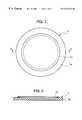
- FIG. 1is a plan view of the carrier used in the semiconductor wafer thinning process of one embodiment of the invention
- FIG. 2is a cross-sectional view taken along a line II—II in FIG. 1,
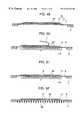
- FIG. 3shows part of the semiconductor wafer processing procedure using the carrier of FIG. 1,
- FIG. 4is another part of the procedure using the carrier of FIG. 1 after the operation of FIG. 3,
- FIG. 5is a schematic diagram of the etching apparatus used in the semiconductor wafer thinning process according to the invention.
- FIG. 6shows another part of the procedure using the carrier after the operation of FIG. 4,
- FIG. 7shows another part of the procedure using the carrier after the operation of FIG. 6,
- FIG. 8shows another part of the procedure using the carrier of FIG. 1 after the operation of FIG. 7,
- FIG. 9shows another part of the procedure using the carrier of FIG. 1 after the operation of FIG. 8,
- FIG. 10shows another part of the procedure using the carrier of FIG. 1 after the operation of FIG. 9,
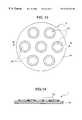
- FIG. 11is a plan view of the carrier used in the semiconductor wafer thinning process according to another embodiment of the invention.
- FIG. 12is a cross-sectional view taken along a line XII—XII in FIG. 11,
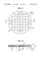
- FIG. 13is a plan view of the carrier used in the semiconductor wafer thinning process according to still another embodiment of the invention.
- FIG. 14is a cross-sectional view taken along a line XIV—XIV in FIG. 13,
- FIG. 15is a plan view of the carrier used in the semiconductor wafer thinning process according to still another embodiment of the invention.
- FIG. 16is a cross-sectional view taken along a line XVI—XVI in FIG. 15,
- FIG. 17is a plan view of the carrier used in the semiconductor wafer thinning process according to still another embodiment of the invention.
- FIG. 18is a cross-sectional view taken along a line XVIII—XVIII in FIG. 17,
- FIG. 19is a plan view of the carrier used in the semiconductor wafer thinning process according to still another embodiment of the invention.
- FIG. 20is a cross-sectional view taken along a line XX—XX in FIG. 19,
- FIG. 21is a plan view of the carrier used in the semiconductor wafer thinning process according to still another embodiment of the invention.
- FIG. 22is a cross-sectional view taken along a line XXII—XXII in FIG. 21,
- FIG. 23shows part of the semiconductor wafer processing procedure using the carrier of FIG. 21,
- FIG. 24shows another part of the semiconductor wafer processing procedure using the carrier of FIG. 21 after the operation of FIG. 23,
- FIG. 25shows another part of the semiconductor wafer processing procedure using the carrier of FIG. 21 after the operation of FIG. 24,
- FIG. 26shows another part of the semiconductor wafer processing procedure using the carrier of FIG. 21 after the operation of FIG. 25,
- FIG. 27shows another part of the semiconductor wafer processing procedure using the carrier of FIG. 21 after the operation of FIG. 26,
- FIG. 28shows another part of the semiconductor wafer processing procedure using the carrier of FIG. 21 after the operation of FIG. 27,
- FIG. 29 ( a )illustrates the state of the bonded semiconductor wafer and carrier
- FIG. 29 ( b )illustrates the state of the separated semiconductor wafer and carrier
- FIG. 30shows another part of the semiconductor wafer processing procedure using the carrier of FIG. 21 after the operation of FIG. 28,
- FIG. 31shows part of the semiconductor wafer processing procedure according to still another embodiment of the invention.
- FIG. 32shows another part of the procedure after the operation of FIG. 31,
- FIG. 33shows another part of the procedure after the operation of FIG. 32
- FIG. 34shows another part of the procedure after the operation of FIG. 33
- FIG. 35shows another part of the procedure after the operation of FIG. 34
- FIG. 36shows another part of the procedure after the operation of FIG. 35
- FIG. 37shows another part of the procedure after the operation of FIG. 36
- FIG. 38is a plan view of the carrier used in the semiconductor wafer thinning process according to still another embodiment of the invention.
- FIG. 39is a cross-sectional view taken along a line XXXIX—XXXIX in FIG. 38,
- FIG. 40is a cross-sectional view of the carrier used in the semiconductor wafer thinning process according to still another embodiment of the invention.
- FIG. 41shows part of the semiconductor wafer processing procedure according to still another embodiment of the invention.
- FIG. 42shows another part of the procedure following the operation of FIG. 41
- FIG. 43shows another part of the procedure following the operation of FIG. 42.
- FIG. 44shows another part of the procedure following the operation of FIG. 43
- FIG. 45shows another part of the procedure following the operation of FIG. 44
- FIG. 46shows another part of the procedure following the operation of FIG. 45.
- FIG. 47shows another part of the procedure following the operation of FIG. 46.
- FIG. 48shows another part of the procedure following the operation of FIG. 47
- FIG. 49shows another part of the procedure following the operation of FIG. 48.
- FIG. 50shows another part of the procedure following the operation of FIG. 49
- FIG. 51shows another part of the procedure following the operation of FIG. 50
- FIG. 52shows another part of the procedure following the operation of FIG. 51
- FIG. 53shows another part of the procedure following the operation of FIG. 52
- FIG. 54shows another part of the procedure following the operation of FIG. 53
- FIG. 55is an enlarged plan view of the chip electrode portion of the semiconductor wafer of FIG. 41.
- FIG. 56is a cross-sectional view taken along a line C 1 —C 1 ,
- FIG. 57shows the details of FIG. 48
- FIG. 58is a plan view of the internal structure of the IC card produced according to this embodiment.
- FIG. 59is a cross-sectional view taken along a line C 2 —C 2 ,
- FIG. 60is an enlarged cross-sectional view of portion A of FIG. 59.
- FIG. 61is an enlarged cross-sectional view of portion B of FIG. 60 .
- FIG. 1is a plan view of the carrier used in the semiconductor wafer thinning process according to one embodiment of the invention
- FIG. 2is a cross-sectional view taken along the line II—II in FIG. 1
- FIG. 3is a cross-sectional view taken along the line II—II in FIG. 1
- FIG. 3is a cross-sectional view taken along the line II—II in FIG. 1
- FIG. 3is a cross-sectional view taken along the line II—II in FIG. 1
- FIG. 3is a cross-sectional view taken along the line II—II in FIG. 1
- FIG. 3is a cross-sectional view taken along the line II—II in FIG. 1
- FIG. 3is a cross-sectional view taken along the line II—II in FIG. 1
- FIG. 3is a cross-sectional view taken along the line II—II in FIG. 1
- FIG. 3is a cross-sectional view taken along the line II—II in FIG. 1
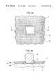
- the carrier 1 depicted in FIGS. 1 and 2has a plate-like shape in order for the semiconductor wafer 2 (shown in FIG. 3 and other figures) to be stuck and held on the carrier to form the wafer composite 10 (as shown in FIG. 3 and other figures).
- This carrier 1is formed of a base 1 a and an elastically flexible suction pad (adhesive member) 1 b provided on one surface of the base 1 a .
- the base 1 a formed in a disk along the shape of the semiconductor wafer 2is made of, for example, fluororesin, glass plate or epoxy resin which has resistance to acid.
- the suction pad 1 b to which the semiconductor wafer 2 is stuckis made of, for example, soft rubber having a size large enough to absorb, or adhere to substantially one entire surface of the semiconductor wafer 2 .
- the base 1 a constituting the carrier 1is preferably made of a material having resistance to acid as described above in order that it can be prevented from changing in quality by an etchant L (FIGS. 5, 6 ).
- the diameter of the base 1 ais designed to be slightly, for example, about 10 ⁇ m larger than the semiconductor wafer 2 .
- the semiconductor wafer 2 stuck on the suction pad 1 bis ground to be thin by the following process.
- the rear surface of the semiconductor wafer 2after the completion of the pretreatment process up to the electric examination for the circuit elements formed on the main surface, is ground to a thickness of, for example, about 250 ⁇ m with a diamond grindstone or abrasive grains. In this case, immediately the thinning process described later may be performed without this preliminary process.
- the semiconductor wafer 2under the condition that its rear surface having no circuit elements is directed to the outside, or opposite to the carrier 1 , is pressed against the carrier 1 as shown in FIG. 3 .
- the suction pad 1 bis elastically deformed so that the volume of the pad closed by the wafer 2 is decreased to discharge the internal air.
- the adhesion pad 1 bintends to be restored by itself to the original shape. As a result, the reduced volume expands somewhat close to the original volume, but air is prevented from flowing into the pad by the wafer 2 that is made in intimate contact with the pad.
- the wafer composite 10is formed (FIG. 4 ). While in this embodiment the semiconductor wafer 2 and carrier 1 constituting the wafer composite 10 are equal in their diameters as depicted in FIG. 4, the wafer 2 may have a smaller diameter than the carrier 1 or may have a larger diameter than carrier as described later.
- a plurality of such wafer composites with their wafers 2 upare enclosed in a cassette case 20 a (FIG. 5 ), and carried to the etching process.
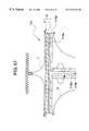
- FIG. 5shows the etching apparatus for the wafer composite 10 .
- the etching apparatusis a spinning-type etcher which coats an etchant L by spinning on the surface of the semiconductor wafer 2 .
- This etching apparatusincludes a loader 30 having the cassette case 20 a , a working stage 50 on which the wafer composite 10 being processed is placed, and an unloader 40 having a cassette case 20 b in which the processed wafer composite 10 is enclosed. Also, it has a handler 60 for carrying the wafer composite 10 from the loader 30 to the working stage 50 , and from the working stage 50 to the unloader 40 .
- the wafer composite 10is carried with its rear surface lifted by this handler 50 .
- an air spout 70is provided beneath the working stage 50 .
- supporting pins 80are provided to grip the wafer composite 10 at, for example, three locations 120 degrees spaced along the peripheral edge of the stage 50 .
- the supporting pins 80can be rotated around the working stage 50 by a motor not shown, and thus the wafer composite 10 is rotated around its rotating axis by the supporting pins 80 .
- a nozzle 90 from which the etchant L is dropped on the semiconductor wafer 2is further provided above the working stage 50 .
- the handler 60picks up one of the wafer composites 10 from the cassette case 20 a that has been set in the loader 30 of the etching apparatus, and loads it on the working stage 50 with its wafer 2 side up.
- the handler 60carries the wafer composite 10 with its rear surface (namely, base 1 a side) lifted, such a shock as to occur when the semiconductor wafer 2 side sucked by vacuum is carried is not added to the semiconductor wafer 2 , and particularly the semiconductor wafer 2 can be prevented from being cracked after the thinning process.
- N 2 gasfor instance, is blown from the gas spout 70 against the wafer composite 10 , to slightly float it from the stage 50 , and it is gripped by the supporting pins 80 when floated. While the N 2 gas is being continuously blown against the wafer composite 10 , the wafer composite 10 is rotated at a rate ranging from a few tens of turns to several thousand turns, and the etchant L is dropped from the nozzle on the semiconductor wafer 2 , thus thinning it as shown in FIG. 6 .
- the nozzle 90be moved at a constant speed up to the outer peripheral edge through the center of the semiconductor wafer 2 while the distance between the nozzle and the wafer is maintained constant.
- the etching speed of the dropped etchant Lis selected to be, for example, 30 ⁇ m/min, and etching time is chosen to be, for example, about 400 seconds.
- the rotation centeris made coincident with the center of the wafer 2 .
- the constituents of etchant L to be chosenare dependent on the purpose of etching, it is desired that, in this embodiment for thinning, the etching rate be selected to be as high as 10 ⁇ m/min to 100 ⁇ m/min. Moreover, when greater importance is attached to the flatness, the etching process may be divided into two steps so that the second etching step can be performed with a lower etching rate. While in this embodiment the etchant L is a mixture of fluoric acid, nitric acid and phosphoric acid, it may be added with a surface active agent for controlling the reaction.
- the semiconductor wafer 2 of the wafer composite 10is etched to be thin up to a thickness of about 50 ⁇ m as shown in FIG. 7 .
- the thicknessis not limited to 50 ⁇ m, but may be arbitrarily selected.
- the semiconductor wafer 2is rinsed with pure water, and dried by rotating it at a high speed of 1000 to 3000 rpm.
- the wafer composite 10is unloaded from the working stage 50 by the handler 60 , and carried into the cassette case 20 b that is provided in the unloader 40 . These processing steps are performed for each of the wafer composites 10 housed in the cassette case 20 a of the loader 30 . After the processed wafer composites are placed in the cassette case 20 b , the cassette case 20 b is taken out from the etching apparatus.
- each wafer composite 10is drawn out from the cassette case 20 b , and stuck on the dicing tape 4 with a ring 3 attached in such a manner that as illustrated in FIG. 8 the rear surface of the wafer 2 can be cemented onto the adhesive surface as in the conventional attachment of wafer 2 on tape.
- the dicing tape 4 usedis formed of, for example, a base made of PET (polyethylene terephthalate), vinyl chloride, polyester or polyethylene, and an adhesive of acrylic polymer coated on the base.
- the base and adhesivemay be other materials.
- the dicing tapemay be of the self-adhesive type in which the base itself has adhesion.
- a peeling jig 5is used to peel off the carrier 1 from the semiconductor wafer 2 .
- the semiconductor wafer 2 50 ⁇ m thickremains stuck to the dicing tape 4 (FIG. 10 ). Under this condition, the semiconductor wafer 2 can be diced into individual semiconductor chips. After dicing, the semiconductor chip or chips are mounted on an IC card through, for example, an anisotropically conductive connection film.
- the semiconductor wafer 2since the semiconductor wafer 2 is stuck to the carrier 1 to form the wafer composite 10 which is then handled for the wafer 2 to be thinned, cracks and warps can be prevented without strict care, and the semiconductor wafer 2 can be stably thinned up to a very small thickness of, for example, 50 ⁇ m.
- the thinned semiconductor wafer 2can be handled as if it were a thick semiconductor wafer before thinning, the semiconductor wafer 2 can be prevented from cracking even without great care, and thus it is easy to work for thinning.
- the semiconductor wafer 2can be prevented from warping due to the stress by the supporting pins 80 , and thus it can be thinned with good quality finishing.
- the semiconductor waferis fixed through the suction pad 1 b to the base 1 a , waste of tape after use, for instance, can be omitted unlike the case of fixing on tape, and the structure of the carrier 1 can be simplified, thus permitting the semiconductor wafer 2 to be thinned at low cost.
- the base 1 aBy making the base 1 a of an acid-resistant material, it is possible to repeatedly use the carrier 1 , so that the semiconductor wafer 2 can be mass-produced at low cost.
- FIG. 11is a plan view of the carrier in another embodiment of the semiconductor wafer thinning process according to the invention.
- FIG. 12is a cross-sectional view taken along the line XII—XII in FIG. 11 .
- the carrier 1has the suction pad 1 b formed in a ring shape along the outer peripheral edge of the semiconductor wafer.
- this carrier 1since the holding force due to the vacuum of suction pad 1 b is exerted only on the outer periphery of the semiconductor wafer, not the inner region, it is possible to suppress the warp in the semiconductor wafer due to the stress on the inner surface region.
- FIG. 13is a plan view of the carrier used in still another embodiment of the semiconductor wafer thinning process according to the invention.
- FIG. 14is a cross-sectional view taken along the line XIV—XIV in FIG. 13 .
- the carrier 1 in this embodimenthas a plurality of suction pads 1 b provided over one entire side of the base 1 a . Therefore, the semiconductor wafer can be supported at a plurality of locations by these suction pads 1 b.
- FIG. 15is a plan view of the carrier used in still another embodiment of the semiconductor wafer thinning process according to the invention.
- FIG. 16is a cross-sectional view taken along the line XVI—XVI in FIG. 15 .
- the carrier 1 in this embodimenthas a smaller diameter than the semiconductor wafer 2 so that the outer peripheral edge of the semiconductor wafer 2 is projected from the carrier 1 .
- the semiconductor wafer 2 of the wafer composite 10overhangs the carrier 1 .
- pin contact projections 1 a 1slightly protruding outward from the semiconductor wafer 2 are formed at three different locations facing the pins along the peripheral edge of the carrier.
- Such a structure as in the overhangs semiconductor wafer 2can be also applied to the carrier 1 in other embodiments.
- the semiconductor wafer 2may be directly supported without the pin contact projections 1 a 1 though it depends on the final thickness of the semiconductor wafer 2 .
- the base 1 ahas a hollow 6 which is communicated with a vacuum hole 6 a connected to a vacuum pump 7 , and a circular suction groove (adhesive member) 11 b for adhering to the semiconductor wafer 2 by vacuum suction is concentrically formed in the surface of the base 1 a so that the center of the groove is coincident with the center of the base 1 a .
- the vacuum hole 6 ahas a valve 8 mounted. This valve 8 is usually closed, but when a nozzle 7 a of the vacuum pump 7 is inserted into the valve, the valve 8 is extended to open the vacuum hole 6 a .
- the suction groove 11 bis not always formed in a concentric circle on the base 1 a , but may be of an arbitrary shape such as a spiral shape. While the valve 8 is provided at the center of the base 1 a as illustrated in FIG. 16, it may be mounted on, for example, the outer peripheral side of the base 1 a . Moreover, the valve 8 may be of a complicated mechanical structure or of a simple elastic type such as rubber.
- the nozzle 7 ais inserted into the vacuum hole 6 a to open the valve 8 of the carrier 1 , and the wafer 2 is attached onto the base 1 a while the hollow 6 is evacuated by the vacuum pump 7 . Then, after enough evacuation is made until the semiconductor wafer 2 can be securely fixed to the base 1 a , the nozzle 7 a is withdrawn from the valve.
- valve 8opens the vacuum hole 6 a to permit air to flow from the hollow 6 to the outside while the nozzle 7 a stays inserted in the valve, but closes the vacuum hole 6 a after the nozzle 7 a is withdrawn from the valve, air can be prevented from flowing from the outside into the hollow 6 so that the semiconductor wafer 2 can be stuck onto the carrier 1 , thus forming the wafer composite 10 .
- the etchant L for thinningis spin-coated on the semiconductor wafer 2 of the wafer composite by the etching apparatus shown in FIG. 5 as described in the previous embodiment.
- N 2 gasfor instance, is continuously blown from below against the wafer composite. Since the semiconductor wafer 2 overhangs from the carrier 1 as described above, the N 2 gas is blown against the downward outer periphery of the main surface of the semiconductor wafer 2 without being blocked by this carrier 1 .
- the wafer compositeis attached onto the dicing tape, and then the vacuum hole is opened so that the pressure in the hollow 6 can be restored to the atmospheric pressure. Accordingly, the suction force of the suction groove 11 b to the semiconductor wafer 2 is lost, thus allowing the carrier 1 to be easily separated from the semiconductor wafer 2 . Then, the semiconductor wafer 2 on the dicing tape is diced into individual semiconductor chips.
- the semiconductor wafer 2 processing technique of this embodimentsince the wafer composite 10 is formed so that the semiconductor wafer 2 overhangs the carrier and since the etchant L for thinning is spin-coated on the semiconductor wafer while air is continuously blown from below against the wafer composite 10 , the etchant L can be prevented from flowing around the peripheral side into the main surface, even though a large centrifugal force cannot be achieved because of spin-coating under a low revolution rate. Therefore, the circuit elements formed on the semiconductor wafer 2 can be protected from being damaged by the etchant.
- the carrier 1can be smoothly peeled off.
- the semiconductor wafer 2is kept flat along the base 1 a , the wafer 2 can be suppressed from warp.
- the diameter of the wafer 2may be smaller than or equal to that of the carrier 1 as is contrary to this embodiment.
- the etchant Lcan be prevented from flowing around the peripheral side into the main surface. Therefore, as in this embodiment, there is no need to spin-coat the etchant L while air is continuously blown against the wafer composite 10 . Also, since the thin semiconductor wafer 2 does not overhang the carrier 1 , it is easy to handle the wafer composite 10 .
- the rear surface of the semiconductor wafer 2can be etched to be thinned by the dipping system in which the wafer composite 10 itself is dipped in the etchant L, not by the spinning type etcher.
- FIG. 17is a plan view of the carrier used in still another embodiment of the semiconductor thinning process according to the invention.
- FIG. 18is a cross-sectional view taken along the line XVIII—XVIII in FIG. 17 .
- suction holes 21 bare provided instead of the suction groove 11 b given in the previous embodiment.
- the suction holes 21 bare formed in one surface of the base 1 a at a plurality of locations so as to be communicated with the vacuum hole 6 a through which the hollow 6 is connected to the vacuum pump as in the sample of the suction groove 11 b .
- the semiconductor wafer 2is sucked by the vacuum pump 7 . Therefore, separation of the semiconductor wafer 2 from the carrier 1 is made by restoration to atmospheric pressure.
- the semiconductor wafer 2may be combined with the carrier 1 to form the wafer composite 10 by the vacuum suction via a plurality of suction holes 21 b thus formed.
- FIG. 19is a plan view of the carrier used in still another embodiment of the semiconductor wafer thinning process according to the invention.
- FIG. 20is a cross-sectional view taken along the line XX—XX in FIG. 19 .
- a porous member 31 b made of resin or metalis provided on one side of the base 1 a instead of the suction groove 11 b .
- the porous member 31 bhas a number of small holes 31 b 1 formed, which are communicated with the vacuum hole 6 a through the hollow 6 as shown in FIG. 20 .
- the semiconductor wafer 2is stuck to the carrier 1 by the vacuum suction via the small holes 31 b 1 of the porous disk 31 b , and separated from the carrier by restoration to atmospheric pressure.
- the semiconductor wafer 2can also be combined with the carrier 1 to form the wafer composite 10 by the vacuum suction via the porous member 31 b.
- FIG. 21is a plan view of the carrier used in still another embodiment of the semiconductor wafer thinning process according to the invention.
- FIG. 22is a cross-sectional diagram taken along the line XXII—XXII in FIG. 21 .
- FIGS. 23 to 28 and FIG. 30are flow diagrams of the semiconductor wafer working process using the carrier shown in FIG. 21 .
- FIGs. 29 ( a ) and 29 ( b )diagrams useful for explaining the sucked state and separated state between the semiconductor wafer and the carrier.
- the adhesion sheet 41 b 1 illustrated in FIG. 22is transparent, a net (exfoliation) 41 b 2 is seen through this adhesion sheet 41 b 1 .
- the adhesion member 41 b of the carrier 1 in this embodimentis formed of the net 41 b 2 having a plurality of small recesses and its surface flush with that of the base 1 a , and the adhesion sheet 41 b 1 interposed between the net 41 b 2 and the semiconductor wafer 2 (FIGS. 23 to 30 ) so as to stick the wafer 2 to the base 1 a .
- the adhesion sheet 41 b 1is made of a flexible, surface-smooth material such as a curable liquid polymer, namely, gelled silicone containing a curable component.
- the base 1 amay have an irregular surface formed as an exfoliative portion.
- a through-hole 1 a 2is formed in the base 1 a at its center, and is connected to the vacuum pump when the semiconductor wafer 2 and the carrier 1 are separated as described later.
- the semiconductor wafer 2 thinned to a certain thicknessis pressed against the carrier 1 .
- the adhesion sheet 41 b 1is required to be completely in contact with the surface of the base 1 a and net 41 b 2 .
- an interfacial forceis exerted between the semiconductor wafer 2 and the adhesion sheet 41 b 1 , causing the semiconductor wafer 2 to stick to the carrier 1 , so that the wafer composite 10 can be formed (FIG. 24 ).
- This wafer composite 10is loaded in the etching apparatus shown in FIG. 5, and the etchant L is pin-coated on the rear surface of the semiconductor wafer 2 of the wafer composite 10 with the semiconductor wafer side up (FIG. 25 ), thereby thinning it (FIG. 26 ). Then, after rinsing and drying, the wafer composite 10 is attached to the dicing tape 4 (FIG. 27 ), and the through-hole 1 a 2 of the base 1 a is connected to the vacuum pump 7 so that the semiconductor wafer is sucked by vacuum (FIG. 28 ).
- the semiconductor wafer 2 and adhesion sheet 41 b 1securely fixed face to face as illustrated in FIG.
- the semiconductor wafer 2 processing technique of this embodimentsince the pressure in the surroundings of the net 41 b 2 is reduced after thinning, thus causing the adhesion sheet 41 b 1 to be pulled into the small recesses of the net 41 b 2 so that the semiconductor wafer 2 and the adhesion sheet 41 b 1 are brought in to the point-contact state under which the interfacial force is reduced to allow the carrier 1 to be separated from the semiconductor wafer 2 , the carrier 1 can be more easily peeled off from the semiconductor wafer 2 , and thus the thin semiconductor wafer 2 can be mass-produced with high productivity.
- the semiconductor wafer 2can always be kept flat along the base 1 a , it is possible to suppress the warp of the semiconductor wafer 2 .
- FIGS. 31 to 37are flow diagrams of the semiconductor wafer thinning process of still another embodiment according to the invention.
- the carrier 1 depicted in FIG. 31has a transparent sheet tape 52 attached to the base 1 a with a transparent adhesive 53 .
- a transparent adhesive 53On the surface of the sheet tape 52 , is coated an adhesive of which the adhesion is reduced or lost by irradiating UV (ultraviolet) light 54 (FIG. 36 ), or a removable UV cure-type adhesive (adhesive member) 51 b .
- the base 1 ais made of a transparent or semitransparent material through which UV light 54 can penetrate, such as acrylic acid resin, or a material having transparency.
- the semiconductor wafer 2 thinned to a certain thicknessis pressed against the UV cure-type adhesive 51 b coated surface of the carrier 1 as illustrated in FIG. 31 .
- the UV cure-type adhesive 51 bis pressed by the semiconductor wafer 2 , thus making the wafer 2 fixed to the carrier 1 to form the wafer composite 10 (FIG. 32 ).
- the wafer composite 10is loaded in the etching apparatus in such a manner that the rear surface of the semiconductor wafer 2 is placed up, and the semiconductor wafer is thinned by dropping the etchant L on the rear surface of the wafer 2 while it is being spun (FIGS. 33 and 34 ).
- the wafer composite 10is attached to the dicing tape 4 (FIG. 35 ), and UV light 54 is irradiated on the wafer composite 10 through the base 1 a (FIG. 36 ).
- the irradiated UV light 54penetrates the transparent base 1 a , sheet tape 52 , and adhesive 53 and reaches the UV cure-type adhesive 51 b . Therefore, adhesion of the UV cure-type adhesive 51 b is reduced by the UV light 54 .
- the carrier 1is pulled away from the semiconductor wafer 2 , and thus the thinned semiconductor wafer 2 stays stuck to the dicing tape 4 (FIG. 37 ). Thereafter, the semiconductor wafer 2 is diced into individual semiconductor chips.
- the dicing tape 4may be made of a material of which the adhesion can be reduced by the irradiation of UV light.
- UV lightis irradiated on the semiconductor wafer when the semiconductor chips after dicing are picked up, the operation is easy.
- the peeling-off operationcan be performed with ease, since UV light 54 , after thinning, is irradiated on the UV cure-type adhesive 51 b used as an adhesive for bonding the semiconductor wafer 2 and the base 1 a , thus reducing its adhesion so that the carrier 1 can be peeled off from the semiconductor wafer 2 .
- the wafer composite 10can be handled like the normal-thickness semiconductor wafer without particular care to the small thickness.
- the semiconductor wafer 2can always be kept flat along the base 1 a , it is possible to suppress the warp of the semiconductor wafer 2 .
- FIG. 38is a plan view of the carrier used in the semiconductor wafer thinning process of still another embodiment according to the invention.
- FIG. 39is a cross-sectional view taken along the line XXXIX—XXXIX in FIG. 38 .
- the carrier 1 in this embodimenthas the base 1 a made of a PET film with a thickness of, for example, 188 ⁇ m, and a temperature activation type adhesive (adhesive member) 61 b , coated on the base 1 a , of which the adhesion is reduced or lost at a low temperature of 0° C. to 5° C.
- the base 1 amay be made of PET film of which the thickness is, for example, 100 ⁇ m or 250 ⁇ m, or made of, for example, a plastic or glass plate other than PET film.
- the temperature activation type adhesive 61 b usedis of the cool-off type in which the peel strength per 25-mm width is 35 gf to 150 gf at a temperature of 10° C.
- the temperature activation type adhesive 61 b in this specificationis an adhesive of which the adhesion is reduced or lost by temperature change, and includes the cool-off type in which the adhesion is reduced at a low temperature as in this embodiment, and a warm-off type of which the adhesion is reduced at a high temperature.
- the semiconductor waferis attached onto the carrier 1 at normal temperature to form the wafer composite, and the semiconductor wafer is thinned by the same etching process as in the previous embodiments. Then, the wafer composite is stuck on the dicing tape so that the adhesive surface adheres to the semiconductor wafer. Thereafter, the wafer composite on the tape is left in a low-temperature environment such as a refrigerator for ten minutes so that the wafer composite is cooled to, for example, 3° C. Since the temperature activation type adhesive 61 b is of the cool-off type in which the peel strength is reduced to about 0 gf at a temperature of 0° C. to 5° C. together with great reduction of the adhesion, the carrier 1 can be easily peeled off from the semiconductor wafer when the wafer composite is cooled to 3° C.
- the temperature activation type adhesive 61 b used in this embodimentis of the cool-off type in which the adhesion is reduced at a low temperature, it may be of the warm-off type in which the adhesion is reduced at a high temperature within a temperature range in which the base 1 a and the dicing tape are not affected by heat.
- the dicing tapeis made of a UV tape of which the adhesion is reduced by the irradiation of UV light, the heat effect can be completely eliminated.
- the peeling-off operationcan be easily performed since the carrier 1 using the temperature activation type adhesive 61 b as a bonding agent is peeled off from the semiconductor wafer when the adhesion is reduced by temperature change.
- the carrier 1since the carrier 1 can be repeatedly used, the thinned semiconductor wafer can be mass-produced at low cost.
- the wafer compositecan be made thin by using PET film for the base 1 a , it can be handled like the normal-thickness semiconductor wafer. Also, since the cost can be reduced, the carrier 1 is disposable.
- the film-shaped base 1 acan be peeled off from the semiconductor wafer, the separation is easier than a plate-like and solid material.
- a protective tape for BG (back grinding) before etching for thinningcan be used for the base 1 a.
- the semiconductor waferis always kept flat along the base 1 a , the warp of the semiconductor wafer can be suppressed even by the carrier 1 of this embodiment.
- FIG. 40is a cross-sectional diagram of the carrier used in the semiconductor wafer thinning process of still another embodiment according to the invention.
- the base 1 a of the carrier 1is made of pressed-hard fibrous fluororesin in place of the PET film described in the above embodiment.
- the bonding agentsuch as the temperature activation type adhesive 61 b can enter into the gaps of the fluororesin by an anchor effect so as to be surely coated on the base 1 a .
- the bonding agent or adhesive membermay be the UV cure-type adhesive 51 b mentioned in the above embodiments.
- the carrier 1since the carrier 1 has its base 1 a made of fluororesin having a feature of resistance to acid, it is possible to use various bonding agents such as the temperature activation type adhesive 61 b that has low adhesion to the base 1 a.
- FIGS. 41 to 54are flow diagrams of an embodiment of the IC card production method according to the invention.
- FIG. 55is an enlarged plan view of the electrode portion of a chip of the semiconductor wafer shown in FIG. 41 .
- FIG. 56is a cross-sectional diagram taken along the line C 1 to C 1 in FIG. 55
- FIG. 57shows the details of FIG. 48
- FIG. 58is a plan view of the internal structure of the IC card produced according to this embodiment.
- FIG. 59is a cross-sectional diagram taken along the line C 2 to C 2 in FIG. 58
- FIG. 60is an enlarged cross-sectional view of portion A in FIG. 59
- FIG. 61is an enlarged cross-sectional view of portion B in FIG. 60 .
- a passivation film 2 a(FIGS. 55 and 56) made of, for example, Si 3 N 4 film is formed on the main surface to shield the circuit elements from the external atmosphere so that the characteristics of the elements can be stabilized.
- Au (gold) bumps 2 bare formed on the chip electrodes by, for example, electrolytic plating or vacuum evaporation.
- the chip electrodesmay be connected to the wiring conductors by wire bonding instead of the bumps.
- bumps made of other metal, such as Pb (phosphorus)/Sn (tin) bumpsmay be formed on the chip electrodes.
- FIG. 55shows the chip electrode of the semiconductor wafer 2 .
- the passivation film 2 ais deposited around the Au bump 2 b on the chip.
- the passivation film 2 a protecting the element region Ais formed of two layers: an inorganic passivation film 2 a as an underlayer and an organic passivation film 2 a 2 as an upper layer.
- the inorganic passivation film 2 a 1is made of, for example, 1.2 ⁇ m-thick SiN (silicon nitride) and 0.6 ⁇ m-thick SiO 2 (silicon oxide), and the organic passivation film 2 a 2 is made of, for example, 2.3 ⁇ m-thick polyimide.
- On the element region Aare formed, for example, an Al electrode conductor 2 c of 0.8 ⁇ m-thickness, and an underbump metal 2 d on the conductor 2 c .
- the Au bump 2 bof, for example, 20 ⁇ m-height is formed on this underbump metal 2 d as a plated electrode.
- the underbump metal 2 dis made of Ti (titanium)/Pd (palladium) for increasing the adhesion and for metal diffusion protection. It may be made of other metals, for example, TiW (titanium-tungsten), Cr (chromium) or Cu (copper).
- a surface-protective resist 111is coated on the main surface of the semiconductor wafer 2 , and heated.
- a BG tape 112 for rear surface grindingis attached on the main surface of the semiconductor wafer 2 , and the rear side of the semiconductor wafer of, for example, 550 ⁇ m thickness is ground to a thickness of, for example, 150 ⁇ m as shown in FIG. 44 . Since the resist 111 is coated on the main surface of the wafer, the surface of the semiconductor wafer 2 can be protected from contamination by dust in the BG process.
- the BG tape 112is peeled off as shown in FIG. 45, and then the resist 111 is removed as shown in FIG. 46 .
- the carrier 1is prepared which has a base made of, for example, 250 ⁇ m-thick PET film and a normal adhesive (namely, not of the temperature activation type) coated on the base. Then, as shown in FIG. 47, the semiconductor wafer 2 with its rear side up is attached onto the carrier 1 to form the wafer composite 10 .
- the carrier 1may be of other types used in the above embodiments.
- the thickness of the adhesive of the carrier 1is equal to the height of the Au bump 2 b , or 20 ⁇ m. Therefore, the adhesive acts not only on the Au bump 2 b , but also on the passivation film 2 a on the wafer surface 20 ⁇ m lower than the Au bump 2 b . Thus, all the entire carrier 1 is made in intimate contact with the semiconductor wafer 2 so that both can be prevented from being peeled off from each other. Since the adhesive adheres to the wafer surface even though its thickness exceeds the height of the Au bump 2 b , the thickness of the adhesive may be larger than the height of the Au bump 2 b (namely, equal to or larger than the height of the Au bump 2 b ).
- the etchant Lis dropped on the rear surface of the semiconductor wafer of the wafer composite with its wafer side up, thinning it by spin etching to a thickness of, for example, 50 ⁇ m.
- the semiconductor waferwould be warped when thinned to such a level because the rigidity of the semiconductor wafer 2 is reduced so that the residual stress in the passivation film 2 a is released.
- the compressing stress in SiN of inorganic passivation film 2 a 1 and the tension stress involved with the curing contraction of polyimide of organic passivation film 2 a 2are released, the surface of the semiconductor wafer 2 would be, creating irregularities.
- the base constituting the carrier 1reinforces the semiconductor wafer 2 to compensate for the reduction of rigidity, and suppresses the release of the stress in the passivation film 2 a , with the result that the thinned semiconductor wafer 2 is never warped.
- the diameter of the semiconductor wafer 2is larger than that of the carrier 1 so that the semiconductor wafer 2 overhangs the carrier 1 .
- an etcher 113 of, for example, pinless chuck typeis used as illustrated in FIG. 57 .
- suction grooves 113 ato be evacuated are formed in the surface of a working stage 113 a at a plurality of locations.
- the suction grooves 113 a 1are communicated with an evacuation groove 113 b 1 of an evacuation tube 113 b connected to a vacuum pump. Since the suction grooves 113 a , are evacuated through the evacuation groove 113 b 1 , the semiconductor wafer 2 is sucked and fixed to the working stage 113 a . Therefore, although the semiconductor wafer 2 overhangs the working stage 113 a , it is not necessary to support its periphery by supporting pins. Thus, the etchant L can be properly dropped on the right place without staying at unnecessary locations of supporting pins, such that defects and dents can be prevented from locally occurring on the semiconductor wafer during etching.
- the diameter of the semiconductor wafer 2may be made smaller than that of the carrier 1 .
- the N 2 gas Gneed not be blown against the wafer composite 10 , and also other etching system such as a dipping system as described above can be employed for thinning the semiconductor wafer 2 .
- the wafer composite 10is attached to the dicing tape 4 with its semiconductor wafer 2 side up as shown in FIG. 49 . Then, as illustrated in FIG. 50, the lower surface of the tape is fixed to a vacuum suction table 114 , and the carrier 1 is peeled off from the semiconductor wafer 2 by peeling.
- the semiconductor wafer 2is divided into individual semiconductor chips P by, for example, full cutting.
- UV light 54is then irradiated on the UV adhesive of the dicing tape 4 , thus reducing or loosing or losing the adhesion between the dicing tape 4 and the semiconductor wafer 2 .
- the card substrate 101is set above the semiconductor chip P, and the semiconductor chip P is tentatively attached by a direct transfer system onto the card substrate 101 at a chip mounting location with the anisotropically conductive adhesive 116 being interposed therebetween.
- the direct transfer systemthe card substrate is stuck up from below by a sticking-up pin 114 .
- the chip Pis fully bonded to the card substrate by a bonding tool 118 with the lower side being supported by a pedestal 117 . In this bonding process, the semiconductor chip is heated and pressed against the card substrate.
- FIG. 58illustrates an IC card 100 formed by the card substrate 101 with the semiconductor chips P thus mounted.
- the IC card 100is a wireless type IC card assembled by a laminate system.
- the IC cardhas its card substrate 101 surrounded by a printed coil 101 b which is formed in a ring shape along the periphery of the IC substrate and which serves as an antenna for receiving an external signal and transmitting an internal signal.
- the IC cardhas also a wiring conductor 110 a formed extending from the printed coil 101 b .
- the wiring conductor 101 aconnects the printed coil 101 b and the semiconductor chips P, so that signals are transmitted and received by the semiconductor chips P having various functions.
- the members of the IC card 100are laminated with an adhesive as shown in FIG. 59 .
- a pacer 102 with recesses provided for receiving the printed coil 101 b , wiring conductor 101 a . and mounted semiconductor chips Pis bonded face to face to the chip-mounded side of the card substrate 101 , so that the spacer 102 is flush with the semiconductor chips P.
- a thickness correcting sheet 103is attached to the spacer 102 so as to adjust the thickness to bring the semiconductor chips P such as IC chips and capacitor chips to the bending neutral point of the IC card 100 (the bending neutral point is the center of the thickness of the IC card 100 if the members of both sides of the semiconductor chip P are all equal).
- the compressing force and tension exerted on the semiconductor chips Pcan be relieved by this thickness correcting sheet.
- decorated exterior plates 104 a , 104 b that serve as the front and rear surfaces of the IC card 100are respectively bonded on both sides of the laminate of card substrate 101 , spacer 102 and thickness correcting sheet 103 .
- the card substrate 101 , thickness correcting sheet 103 and decorated exterior plates 104 a , 104 bare made of PFT.
- FIG. 60is an enlarged view of portion A of FIG. 59 .
- the Au bumps 2 bare electrically connected to the wiring conductor 101 a . through the anisotropically conductive adhesive 116 and by its adhesion so that the semiconductors P are mounted on the card substrate 101 .
- the thickness correcting sheet 103is bonded to the card substrate 101 with the spacer 102 interposed therebetween.
- FIG. 61is an enlarged view of portion B of FIG. 60 .
- the anisotropically conductive adhesive 116is formed by an adhesive 116 b and conductive particles 116 a each of which is formed of, for example, a plastic ball of about 5 ⁇ m-diameter with an Au coating.
- each of the conductive particles 116 a of the anisotropically conductive adhesive 116are pressed between the Au bump 2 b and the wiring conductor 101 a .
- the Au bump 2 b and the wiring conductor 101 acan be electrically connected through the crushed conductive particles 116 a.
- the carrier 1 and the semiconductor wafer 2are combined into the wafer composite 10 of which the semiconductor wafer 2 is then thinned to a thickness of, for example, 50 ⁇ m without any crack or warp, and diced into semiconductor chips P which are used in the assembly process for the IC card 100 , the IC card 100 can be made thinner.
- the base 1 amay be molded out of fluororesin, glass plate or epoxy resin, and the suction pad 1 b may be a liquid such as water.
- the interfacial forceis exerted between the semiconductor wafer 2 and the base 1 a so that both materials can be bonded together, and in order to peel the carrier 1 from the semiconductor wafer 2 , ultrasonic wave is applied to the wafer composite.
- the semiconductor wafer processing technique of the inventionis useful for the application to the semiconductor chips incorporated in ultra-thin type electronic devices such as IC cards.
Landscapes
- Engineering & Computer Science (AREA)
- Microelectronics & Electronic Packaging (AREA)
- Computer Hardware Design (AREA)
- Physics & Mathematics (AREA)
- General Physics & Mathematics (AREA)
- Power Engineering (AREA)
- Theoretical Computer Science (AREA)
- Condensed Matter Physics & Semiconductors (AREA)
- Manufacturing & Machinery (AREA)
- Computer Networks & Wireless Communication (AREA)
- Container, Conveyance, Adherence, Positioning, Of Wafer (AREA)
- Weting (AREA)
Abstract
Description
Claims (4)
Priority Applications (2)
| Application Number | Priority Date | Filing Date | Title |
|---|---|---|---|
| US09/991,750US6589855B2 (en) | 1995-12-04 | 2001-11-26 | Methods of processing semiconductor wafer and producing IC card, and carrier |
| US09/991,747US6573158B2 (en) | 1995-12-04 | 2001-11-26 | Methods of processing semiconductor wafer and producing IC card, and carrier |
Applications Claiming Priority (3)
| Application Number | Priority Date | Filing Date | Title |
|---|---|---|---|
| JP31508995 | 1995-12-04 | ||
| JP7-315089 | 1995-12-04 | ||
| PCT/JP1996/002863WO1997021243A1 (en) | 1995-12-04 | 1996-10-02 | Method for processing semiconductor wafer, method for manufacturing ic card, and carrier |
Related Child Applications (2)
| Application Number | Title | Priority Date | Filing Date |
|---|---|---|---|
| US09/991,750ContinuationUS6589855B2 (en) | 1995-12-04 | 2001-11-26 | Methods of processing semiconductor wafer and producing IC card, and carrier |
| US09/991,747ContinuationUS6573158B2 (en) | 1995-12-04 | 2001-11-26 | Methods of processing semiconductor wafer and producing IC card, and carrier |
Publications (1)
| Publication Number | Publication Date |
|---|---|
| US6342434B1true US6342434B1 (en) | 2002-01-29 |
Family
ID=18061281
Family Applications (3)
| Application Number | Title | Priority Date | Filing Date |
|---|---|---|---|
| US09/077,548Expired - LifetimeUS6342434B1 (en) | 1995-12-04 | 1996-02-10 | Methods of processing semiconductor wafer, and producing IC card, and carrier |
| US09/991,747Expired - LifetimeUS6573158B2 (en) | 1995-12-04 | 2001-11-26 | Methods of processing semiconductor wafer and producing IC card, and carrier |
| US09/991,750Expired - LifetimeUS6589855B2 (en) | 1995-12-04 | 2001-11-26 | Methods of processing semiconductor wafer and producing IC card, and carrier |
Family Applications After (2)
| Application Number | Title | Priority Date | Filing Date |
|---|---|---|---|
| US09/991,747Expired - LifetimeUS6573158B2 (en) | 1995-12-04 | 2001-11-26 | Methods of processing semiconductor wafer and producing IC card, and carrier |
| US09/991,750Expired - LifetimeUS6589855B2 (en) | 1995-12-04 | 2001-11-26 | Methods of processing semiconductor wafer and producing IC card, and carrier |
Country Status (8)
| Country | Link |
|---|---|
| US (3) | US6342434B1 (en) |
| EP (1) | EP0866494A4 (en) |
| KR (1) | KR19990071818A (en) |
| CN (1) | CN1203696A (en) |
| AU (1) | AU729849B2 (en) |
| CA (1) | CA2238974A1 (en) |
| TW (1) | TW328141B (en) |
| WO (1) | WO1997021243A1 (en) |
Cited By (59)
| Publication number | Priority date | Publication date | Assignee | Title |
|---|---|---|---|---|
| US20020056927A1 (en)* | 1999-09-22 | 2002-05-16 | Shinji Ohuchi | Method of making semiconductor device having first and second sealing resins |
| US6426275B1 (en) | 1999-08-03 | 2002-07-30 | Tokyo Seimitsu Co., Ltd. | Method for manufacturing semiconductor chips using protecting pricing and separating sheets |
| US20020166625A1 (en)* | 2001-05-14 | 2002-11-14 | Ball Michael B. | Using backgrind wafer tape to enable wafer mounting of bumped wafers |
| US20030082915A1 (en)* | 2000-08-04 | 2003-05-01 | Sharp Kabushiki Kaisha | Method of thinning semiconductor wafer capable of preventing its front from being contaminated and back grinding device for semiconductor wafers |
| US20030109137A1 (en)* | 2000-10-25 | 2003-06-12 | Hayato Iwamoto | Method for manufacturing semiconductor device |
| US6642126B2 (en)* | 1999-12-22 | 2003-11-04 | Micronas Gmbh | Process for manufacturing a semiconductor wafer with passivation layer mask for etching with mechanical removal |
| US20040020338A1 (en)* | 2002-06-10 | 2004-02-05 | Yuuji Ookawa | Adhesive sheet for dicing glass substrate and method of dicing glass substrate |
| US20040048445A1 (en)* | 2002-09-06 | 2004-03-11 | Motorola, Inc. | Thinned semiconductor wafer and die and corresponding method |
| US20040266159A1 (en)* | 2003-06-28 | 2004-12-30 | International Business Machines Corporation | Method for forming interconnects on thin wafers |
| US20050006767A1 (en)* | 2001-06-29 | 2005-01-13 | Takashi Kumamoto | Multi-purpose planarizing/back-grind/pre-underfill arrangements for bumped wafers and dies |
| US20050019980A1 (en)* | 2003-03-26 | 2005-01-27 | Tetsuya Kurosawa | Semiconductor manufacturing apparatus and method of manufacturing semiconductor device |
| US20050136653A1 (en)* | 2003-12-22 | 2005-06-23 | Ramirez Jose G. | Non-adhesive semiconductor wafer holder and assembly |
| US20050147489A1 (en)* | 2003-12-24 | 2005-07-07 | Tian-An Chen | Wafer supporting system for semiconductor wafers |
| US20050227414A1 (en)* | 2004-04-07 | 2005-10-13 | Optimum Care International Tech. Inc. | Packaging method for integrated circuits |
| US20050250295A1 (en)* | 2002-06-25 | 2005-11-10 | Humiaki Mita | Semiconductor device manufacturing method and ring-shaped reinforcing member |
| US20050281056A1 (en)* | 2004-05-25 | 2005-12-22 | Loomis Jason A | Ornament lighting apparatus |
| US20060011288A1 (en)* | 2004-07-16 | 2006-01-19 | Semiconductor Energy | Laminating system, IC sheet, roll of IC sheet, and method for manufacturing IC chip |
| US20060040467A1 (en)* | 2004-08-20 | 2006-02-23 | Dolechek Kert L | Process and apparatus for thinning a semiconductor workpiece |
| US20060040111A1 (en)* | 2004-08-20 | 2006-02-23 | Dolechek Kert L | Process chamber and system for thinning a semiconductor workpiece |
| US20060046499A1 (en)* | 2004-08-20 | 2006-03-02 | Dolechek Kert L | Apparatus for use in thinning a semiconductor workpiece |
| US20060118515A1 (en)* | 2004-08-20 | 2006-06-08 | Semitool, Inc. | Process For Thinning A Semiconductor Workpiece |
| US20060138683A1 (en)* | 2004-12-24 | 2006-06-29 | Chih-Ming Hsu | Fabrication method of light emitting diodes |
| US20060263941A1 (en)* | 2005-05-17 | 2006-11-23 | Oki Electric Industry Co., Ltd. | Method of manufacturing semiconductor device and method of manufacturing bonding sheet |
| US20070036932A1 (en)* | 2005-07-19 | 2007-02-15 | Micron Technology, Inc. | Methods for releasably attaching support members to microfeature workpieces and microfeature assemblies formed using such methods |
| US20070117351A1 (en)* | 2004-04-15 | 2007-05-24 | Stephan Bradl | Method for machining a workpiece on a workpiece support |
| US20070238222A1 (en)* | 2006-03-28 | 2007-10-11 | Harries Richard J | Apparatuses and methods to enhance passivation and ILD reliability |
| US20070241078A1 (en)* | 2006-03-14 | 2007-10-18 | Micron Technology, Inc. | Methods for releasably attaching support members to microfeature workpieces |
| US20080044940A1 (en)* | 2004-06-02 | 2008-02-21 | Ryosuke Watanabe | Laminating System |
| US20080042168A1 (en)* | 2004-07-30 | 2008-02-21 | Semiconductor Energy Laboratory Co., Ltd. | Laminating System, Ic Sheet, Scroll of Ic Sheet, and Method for Manufacturing Ic Chip |
| US20080057625A1 (en)* | 2006-08-31 | 2008-03-06 | Ati Technologies Inc. | Method and apparatus for making semiconductor packages |
| US7354649B2 (en) | 2004-08-20 | 2008-04-08 | Semitool, Inc. | Semiconductor workpiece |
| US20090091044A1 (en)* | 2006-02-14 | 2009-04-09 | Joon-Mo Seo | Dicing die attachment film and method for packaging semiconductor using same |
| US20090186216A1 (en)* | 2003-06-06 | 2009-07-23 | Teiichi Inada | Adhesive sheet, dicing tape integrated type adhesive sheet, and method of producing semiconductor device |
| US20090218560A1 (en)* | 2008-01-24 | 2009-09-03 | Brewer Science Inc. | Method for reversibly mounting a device wafer to a carrier substrate |
| US20090297867A1 (en)* | 2008-06-03 | 2009-12-03 | Sumco Corporation | Semiconductor thin film-attached substrate and production method thereof |
| US20100194014A1 (en)* | 2009-02-02 | 2010-08-05 | Jao Sheng Huang | Semiconductor Wafer Carrier |
| US20100236053A1 (en)* | 2006-02-03 | 2010-09-23 | Semiconductor Energy Laboratory Co., Ltd. | Apparatus and method for manufacturing semiconductor device |
| US20110018114A1 (en)* | 2009-07-22 | 2011-01-27 | Stats Chippac, Ltd. | Semiconductor Device and Method of Embedding Thermally Conductive Layer in Interconnect Structure for Heat Dissipation |
| EP2290679A1 (en)* | 2009-09-01 | 2011-03-02 | EV Group GmbH | Device and method for releasing a semiconductor wafer from a support substrate |
| EP2381464A1 (en)* | 2010-04-23 | 2011-10-26 | EV Group GmbH | Device and method for releasing a product substrate from a holder substrate |
| WO2011162778A1 (en)* | 2010-06-21 | 2011-12-29 | Brewer Science Inc. | Method and apparatus for removing a reversibly mounted device wafer from a carrier substrate |
| US20120329369A1 (en)* | 2011-06-27 | 2012-12-27 | Kabushiki Kaisha Toshiba | Substrate processing method and substrate processing apparatus |
| US8443864B2 (en) | 2009-03-18 | 2013-05-21 | Ev Group Gmbh | Device for stripping a wafer from a carrier |
| US20130133688A1 (en)* | 2011-11-29 | 2013-05-30 | Taiwan Semiconductor Manufacturing Company, Ltd. | Wafer debonding and cleaning apparatus and method of use |
| US8536020B2 (en) | 2006-01-03 | 2013-09-17 | Erich Thallner | Combination of a substrate and a wafer |
| US20130330910A1 (en)* | 2010-10-01 | 2013-12-12 | Shumpei Tanaka | Dicing die bond film and method of manufacturing semiconductor device |
| US20140311663A1 (en)* | 2013-04-23 | 2014-10-23 | Sumika Technology Co., Ltd. | Method of fabricating flexible color filter and flexible color display device |
| US20140374031A1 (en)* | 2011-11-29 | 2014-12-25 | Taiwan Semiconductor Manufacturing Company, Ltd. | Wafer debonding and cleaning apparatus and method |
| US8951886B2 (en) | 2008-12-23 | 2015-02-10 | Thin Materials Ag | Method for separating a layer system comprising a wafer by precisely maintaining the position of the separating front |
| US20150044857A1 (en)* | 2013-08-07 | 2015-02-12 | Disco Corporation | Dividing method for wafer |
| FR3012257A1 (en)* | 2013-10-21 | 2015-04-24 | Soitec Silicon On Insulator | PROCESS FOR PREHENDING A SUBSTRATE |
| US9211691B2 (en)* | 2012-09-19 | 2015-12-15 | Tokyo Electron Limited | Delamination device |
| US9263314B2 (en) | 2010-08-06 | 2016-02-16 | Brewer Science Inc. | Multiple bonding layers for thin-wafer handling |
| US10559486B1 (en)* | 2018-01-10 | 2020-02-11 | Facebook Technologies, Llc | Method for polymer-assisted chip transfer |
| US10586725B1 (en)* | 2018-01-10 | 2020-03-10 | Facebook Technologies, Llc | Method for polymer-assisted chip transfer |
| US11105752B2 (en)* | 2019-04-16 | 2021-08-31 | Disco Corporation | Inspecting apparatus and processing apparatus including the same |
| US11188805B2 (en) | 2004-07-30 | 2021-11-30 | Semiconductor Energy Laboratory Co., Ltd. | Lamination system, IC sheet, scroll of IC sheet, and method for manufacturing IC chip |
| US11264262B2 (en)* | 2011-11-29 | 2022-03-01 | Taiwan Semiconductor Manufacturing Company, Ltd. | Wafer debonding and cleaning apparatus |
| TWI820751B (en)* | 2021-06-18 | 2023-11-01 | 穩懋半導體股份有限公司 | Method of transferring light-emitting elemet |
Families Citing this family (58)
| Publication number | Priority date | Publication date | Assignee | Title |
|---|---|---|---|---|
| DE19921230B4 (en)* | 1999-05-07 | 2009-04-02 | Giesecke & Devrient Gmbh | Method for handling thinned chips for insertion in chip cards |
| US6140146A (en)* | 1999-08-03 | 2000-10-31 | Intermec Ip Corp. | Automated RFID transponder manufacturing on flexible tape substrates |
| JP4546626B2 (en)* | 2000-08-29 | 2010-09-15 | 株式会社ディスコ | Method for picking up semiconductor element |
| JP2002075937A (en)* | 2000-08-30 | 2002-03-15 | Nitto Denko Corp | Semiconductor wafer processing method |
| JP2002092575A (en)* | 2000-09-19 | 2002-03-29 | Mitsubishi Electric Corp | Small card and its manufacturing method |
| JP3892703B2 (en)* | 2001-10-19 | 2007-03-14 | 富士通株式会社 | Semiconductor substrate jig and semiconductor device manufacturing method using the same |
| JP3880397B2 (en)* | 2001-12-27 | 2007-02-14 | 日東電工株式会社 | How to apply and peel off protective tape |
| US6908784B1 (en)* | 2002-03-06 | 2005-06-21 | Micron Technology, Inc. | Method for fabricating encapsulated semiconductor components |
| US6881675B2 (en)* | 2002-05-15 | 2005-04-19 | Taiwan Semiconductor Manufacturing Co, Ltd. | Method and system for reducing wafer edge tungsten residue utilizing a spin etch |
| JP2004014956A (en)* | 2002-06-11 | 2004-01-15 | Shinko Electric Ind Co Ltd | Work processing method of micro semiconductor device |
| US6903442B2 (en)* | 2002-08-29 | 2005-06-07 | Micron Technology, Inc. | Semiconductor component having backside pin contacts |
| JP3748844B2 (en)* | 2002-09-25 | 2006-02-22 | Necエレクトロニクス株式会社 | Semiconductor integrated circuit and test method thereof |
| US7288465B2 (en)* | 2003-04-15 | 2007-10-30 | International Business Machines Corpoartion | Semiconductor wafer front side protection |
| EP1494167A1 (en)* | 2003-07-04 | 2005-01-05 | Koninklijke Philips Electronics N.V. | Flexible semiconductor device and identification label |
| JP2005039114A (en)* | 2003-07-17 | 2005-02-10 | Disco Abrasive Syst Ltd | Semiconductor wafer transfer equipment |
| JP4405211B2 (en)* | 2003-09-08 | 2010-01-27 | パナソニック株式会社 | Semiconductor chip peeling apparatus, peeling method, and semiconductor chip supply apparatus |
| DE20318462U1 (en) | 2003-11-26 | 2004-03-11 | Infineon Technologies Ag | Arrangement of electronic semiconductor components on a carrier system for treating the semiconductor components with a liquid medium |
| DE102004018250A1 (en)* | 2004-04-15 | 2005-11-03 | Infineon Technologies Ag | Wafer stabilization device and method for its production |
| JP4306540B2 (en)* | 2004-06-09 | 2009-08-05 | セイコーエプソン株式会社 | Thin processing method of semiconductor substrate |
| KR100574983B1 (en)* | 2004-07-06 | 2006-05-02 | 삼성전자주식회사 | Semiconductor Wafer Processing Method for Semiconductor Device Manufacturing |
| US20060046433A1 (en)* | 2004-08-25 | 2006-03-02 | Sterrett Terry L | Thinning semiconductor wafers |
| US7049208B2 (en) | 2004-10-11 | 2006-05-23 | Intel Corporation | Method of manufacturing of thin based substrate |
| CN101116180B (en)* | 2005-02-03 | 2011-08-17 | 信越聚合物株式会社 | Fixation carrier, production method of fixation carrier, use method of fixation carrier, and substrate reception container |
| JP4613709B2 (en)* | 2005-06-24 | 2011-01-19 | セイコーエプソン株式会社 | Manufacturing method of semiconductor device |
| US20070217119A1 (en)* | 2006-03-17 | 2007-09-20 | David Johnson | Apparatus and Method for Carrying Substrates |
| US20070246839A1 (en)* | 2006-04-21 | 2007-10-25 | Applied Materials, Inc. | Method of proximity pin manufacture |
| KR100817718B1 (en)* | 2006-12-27 | 2008-03-27 | 동부일렉트로닉스 주식회사 | Semiconductor device manufacturing method |
| US7851333B2 (en)* | 2007-03-15 | 2010-12-14 | Infineon Technologies Ag | Apparatus comprising a device and method for producing it |
| JP4746003B2 (en)* | 2007-05-07 | 2011-08-10 | リンテック株式会社 | Transfer device and transfer method |
| US7767557B2 (en)* | 2007-05-11 | 2010-08-03 | Micron Technology, Inc. | Chilled wafer dicing |
| US7816232B2 (en)* | 2007-11-27 | 2010-10-19 | Semiconductor Energy Laboratory Co., Ltd. | Method for manufacturing semiconductor substrate and semiconductor substrate manufacturing apparatus |
| US20090191029A1 (en)* | 2008-01-30 | 2009-07-30 | Taeg Ki Lim | System for handling semiconductor dies |
| JP5417729B2 (en)* | 2008-03-28 | 2014-02-19 | 住友ベークライト株式会社 | Film for semiconductor, method for manufacturing semiconductor device, and semiconductor device |
| CN101939825B (en) | 2008-02-07 | 2013-04-03 | 住友电木株式会社 | Film for semiconductor, method for manufacturing semiconductor device and semiconductor device |
| US7972969B2 (en)* | 2008-03-06 | 2011-07-05 | Taiwan Semiconductor Manufacturing Co., Ltd. | Method and apparatus for thinning a substrate |
| DE102008024790A1 (en)* | 2008-05-23 | 2009-12-10 | Smartrac Ip B.V. | Antenna arrangement for a chip card |
| TWI439351B (en)* | 2008-09-29 | 2014-06-01 | Nitto Denko Corp | Adsorption tablets |
| JP2009094539A (en)* | 2009-01-21 | 2009-04-30 | Disco Abrasive Syst Ltd | Method for dividing CSP substrate |
| CN101722470B (en)* | 2009-11-24 | 2011-09-28 | 成都东骏激光股份有限公司 | Method for manufacturing large-size ultra-thin laser crystal |
| US8563405B2 (en) | 2010-05-06 | 2013-10-22 | Ineffable Cellular Limited Liability Company | Method for manufacturing semiconductor device |
| CN103249562B (en)* | 2010-12-09 | 2015-07-08 | 旭化成电子材料株式会社 | Fine-structure laminate, method for preparing fine-tructure laminate, and production method for fine-structure laminate |
| CN102339780B (en)* | 2011-09-30 | 2013-07-17 | 格科微电子(上海)有限公司 | Adsorbing and supporting device of wafer and substrate and semiconductor processing equipment of wafer |
| DE102012001345A1 (en)* | 2012-01-24 | 2013-07-25 | Giesecke & Devrient Gmbh | Method for producing a data carrier |
| JP5591859B2 (en)* | 2012-03-23 | 2014-09-17 | 株式会社東芝 | Substrate separation method and separation apparatus |
| JP6035468B2 (en)* | 2012-07-03 | 2016-11-30 | アールエフエイチアイシー コーポレイション | Semiconductor-on-diamond wafer handle and manufacturing method |
| JP5970986B2 (en)* | 2012-07-05 | 2016-08-17 | 富士通株式会社 | Manufacturing method of wafer substrate |
| US9331230B2 (en)* | 2012-10-30 | 2016-05-03 | Cbrite Inc. | LED die dispersal in displays and light panels with preserving neighboring relationship |
| US9543197B2 (en)* | 2012-12-19 | 2017-01-10 | Intel Corporation | Package with dielectric or anisotropic conductive (ACF) buildup layer |
| US9013039B2 (en)* | 2013-08-05 | 2015-04-21 | Globalfoundries Inc. | Wafer support system for 3D packaging |
| US9613842B2 (en) | 2014-02-19 | 2017-04-04 | Globalfoundries Inc. | Wafer handler and methods of manufacture |
| KR102427159B1 (en) | 2015-11-11 | 2022-08-01 | 삼성전자주식회사 | apparatus for laminating tape film on the substrate and equipment for manufacturing semiconductor device including the same |
| US9997399B2 (en)* | 2016-08-16 | 2018-06-12 | Mikro Mesa Technology Co., Ltd. | Method for transferring semiconductor structure |
| KR102450310B1 (en) | 2017-11-27 | 2022-10-04 | 삼성전자주식회사 | Semiconductor chip and multi-chip package having the same |
| US11041879B2 (en) | 2019-06-06 | 2021-06-22 | International Business Machines Corporation | Fluidized alignment of a semiconductor die to a test probe |
| TW202347464A (en)* | 2020-03-23 | 2023-12-01 | 日商捷進科技有限公司 | Die bonding device, peeling jig and manufacturing method of semiconductor device |
| CN111453997A (en)* | 2020-04-14 | 2020-07-28 | 拓米(成都)应用技术研究院有限公司 | Method for manufacturing ultrathin glass by single-side etching and ultrathin glass |
| CN112105166B (en)* | 2020-09-02 | 2024-03-29 | 深圳市鑫达辉软性电路科技有限公司 | FPC warp prosthetic devices |
| DE112022004060T5 (en)* | 2022-04-27 | 2024-08-01 | Yamaha Hatsudoki Kabushiki Kaisha | Expansion device, method for manufacturing semiconductor chips and semiconductor chip |
Citations (25)
| Publication number | Priority date | Publication date | Assignee | Title |
|---|---|---|---|---|
| US3861978A (en) | 1973-03-08 | 1975-01-21 | Western Electric Co | Method of joining two bodies after treatment with an inorganic colloid |
| JPS55160440A (en) | 1979-05-31 | 1980-12-13 | Chiyou Lsi Gijutsu Kenkyu Kumiai | Device for fixing thin plate |
| US4339297A (en)* | 1981-04-14 | 1982-07-13 | Seiichiro Aigo | Apparatus for etching of oxide film on semiconductor wafer |
| JPS62193725A (en) | 1986-02-20 | 1987-08-25 | Inoue Japax Res Inc | Wire cut electric discharge machine |
| JPS63256342A (en) | 1987-04-10 | 1988-10-24 | Sumitomo Electric Ind Ltd | Grinding method for semiconductor wafers |
| EP0312924A2 (en)* | 1987-10-22 | 1989-04-26 | Fujitsu Limited | Vacuum chucking tool and system |
| JPH01134945A (en) | 1987-11-19 | 1989-05-26 | Tokyo Electron Ltd | Wafer holding device |
| EP0318862A2 (en) | 1987-11-26 | 1989-06-07 | Nitto Boseki Co., Ltd. | Glass fiber product for use in the reinforcement of fluororesin |
| JPH02309638A (en) | 1989-05-24 | 1990-12-25 | Fujitsu Ltd | wafer etching equipment |
| DE4002018A1 (en) | 1990-01-24 | 1991-07-25 | Helmut K Rohrer | Easy electronic chip release from wafer support foil - which is deposited onto surfaces with structural depression, with foil top side exposed to overpressure |
| JPH03256677A (en) | 1990-03-02 | 1991-11-15 | Sony Corp | Thin piece suction holding device |
| US5155068A (en) | 1989-08-31 | 1992-10-13 | Sharp Kabushiki Kaisha | Method for manufacturing an IC module for an IC card whereby an IC device and surrounding encapsulant are thinned by material removal |
| JPH0567371A (en) | 1991-08-02 | 1993-03-19 | Sony Corp | Recording and reproducing device |
| JPH0582631A (en) | 1991-09-20 | 1993-04-02 | Toshiba Ceramics Co Ltd | Vacuum chuck for semiconductor wafer |
| US5238876A (en)* | 1989-07-21 | 1993-08-24 | Mitsubishi Denki Kabushiki Kaisha | Method of dividing semiconductor wafer using ultraviolet sensitive tape |
| US5268065A (en)* | 1992-12-21 | 1993-12-07 | Motorola, Inc. | Method for thinning a semiconductor wafer |
| JPH0661202A (en) | 1991-10-28 | 1994-03-04 | Shin Etsu Chem Co Ltd | Method of holding semiconductor wafer |
| JPH06177099A (en) | 1992-12-02 | 1994-06-24 | Toshiba Corp | Thinning method for semiconductor pellets |
| EP0622833A1 (en) | 1993-04-28 | 1994-11-02 | Texas Instruments Incorporated | Adhesive sheet for wafer and process for preparing semiconductor apparatus using the same |
| JPH0745583A (en) | 1993-07-30 | 1995-02-14 | Shin Etsu Handotai Co Ltd | High-flatness etching of wafer and device |
| JPH07106285A (en) | 1993-10-08 | 1995-04-21 | Oki Electric Ind Co Ltd | Manufacture of semiconductor device |
| JPH08181092A (en) | 1994-12-26 | 1996-07-12 | Sumitomo Metal Ind Ltd | Holding plate for polishing semiconductor wafers |
| EP0828292A1 (en) | 1995-05-18 | 1998-03-11 | Hitachi, Ltd. | Semiconductor device and its manufacture |
| US5877034A (en)* | 1994-09-22 | 1999-03-02 | Fraunhofer Gesellschaft Zur Foerderung Der Angwandten Forschung E.V. | Method of making a three-dimensional integrated circuit |
| US5897337A (en)* | 1994-09-30 | 1999-04-27 | Nec Corporation | Process for adhesively bonding a semiconductor chip to a carrier film |
Family Cites Families (4)
| Publication number | Priority date | Publication date | Assignee | Title |
|---|---|---|---|---|
| JPS6133831A (en)* | 1984-07-24 | 1986-02-17 | Citizen Watch Co Ltd | Vacuum adsorption device |
| JPS62193725U (en)* | 1986-05-30 | 1987-12-09 | ||
| JPS63256354A (en)* | 1987-04-14 | 1988-10-24 | Mitsubishi Electric Corp | High-precision polishing method for composite materials |
| FR2759330B1 (en) | 1997-02-13 | 1999-04-30 | Faure Bertrand Equipements Sa | MOTOR VEHICLE SEAT SLIDE |
- 1996
- 1996-02-10USUS09/077,548patent/US6342434B1/ennot_activeExpired - Lifetime
- 1996-10-02EPEP96932799Apatent/EP0866494A4/ennot_activeWithdrawn
- 1996-10-02WOPCT/JP1996/002863patent/WO1997021243A1/ennot_activeApplication Discontinuation
- 1996-10-02KRKR1019980704098Apatent/KR19990071818A/ennot_activeWithdrawn
- 1996-10-02AUAU71447/96Apatent/AU729849B2/ennot_activeCeased
- 1996-10-02CACA002238974Apatent/CA2238974A1/ennot_activeAbandoned
- 1996-10-02CNCN96198789Apatent/CN1203696A/enactivePending
- 1996-11-11TWTW085113772Apatent/TW328141B/ennot_activeIP Right Cessation
- 2001
- 2001-11-26USUS09/991,747patent/US6573158B2/ennot_activeExpired - Lifetime
- 2001-11-26USUS09/991,750patent/US6589855B2/ennot_activeExpired - Lifetime
Patent Citations (26)
| Publication number | Priority date | Publication date | Assignee | Title |
|---|---|---|---|---|
| US3861978A (en) | 1973-03-08 | 1975-01-21 | Western Electric Co | Method of joining two bodies after treatment with an inorganic colloid |
| JPS55160440A (en) | 1979-05-31 | 1980-12-13 | Chiyou Lsi Gijutsu Kenkyu Kumiai | Device for fixing thin plate |
| US4339297A (en)* | 1981-04-14 | 1982-07-13 | Seiichiro Aigo | Apparatus for etching of oxide film on semiconductor wafer |
| JPS62193725A (en) | 1986-02-20 | 1987-08-25 | Inoue Japax Res Inc | Wire cut electric discharge machine |
| JPS63256342A (en) | 1987-04-10 | 1988-10-24 | Sumitomo Electric Ind Ltd | Grinding method for semiconductor wafers |
| EP0312924A2 (en)* | 1987-10-22 | 1989-04-26 | Fujitsu Limited | Vacuum chucking tool and system |
| JPH01134945A (en) | 1987-11-19 | 1989-05-26 | Tokyo Electron Ltd | Wafer holding device |
| EP0318862A2 (en) | 1987-11-26 | 1989-06-07 | Nitto Boseki Co., Ltd. | Glass fiber product for use in the reinforcement of fluororesin |
| JPH02309638A (en) | 1989-05-24 | 1990-12-25 | Fujitsu Ltd | wafer etching equipment |
| US5238876A (en)* | 1989-07-21 | 1993-08-24 | Mitsubishi Denki Kabushiki Kaisha | Method of dividing semiconductor wafer using ultraviolet sensitive tape |
| US5155068A (en) | 1989-08-31 | 1992-10-13 | Sharp Kabushiki Kaisha | Method for manufacturing an IC module for an IC card whereby an IC device and surrounding encapsulant are thinned by material removal |
| DE4002018A1 (en) | 1990-01-24 | 1991-07-25 | Helmut K Rohrer | Easy electronic chip release from wafer support foil - which is deposited onto surfaces with structural depression, with foil top side exposed to overpressure |
| JPH03256677A (en) | 1990-03-02 | 1991-11-15 | Sony Corp | Thin piece suction holding device |
| JPH0567371A (en) | 1991-08-02 | 1993-03-19 | Sony Corp | Recording and reproducing device |
| JPH0582631A (en) | 1991-09-20 | 1993-04-02 | Toshiba Ceramics Co Ltd | Vacuum chuck for semiconductor wafer |
| JPH0661202A (en) | 1991-10-28 | 1994-03-04 | Shin Etsu Chem Co Ltd | Method of holding semiconductor wafer |
| JPH06177099A (en) | 1992-12-02 | 1994-06-24 | Toshiba Corp | Thinning method for semiconductor pellets |
| US5268065A (en)* | 1992-12-21 | 1993-12-07 | Motorola, Inc. | Method for thinning a semiconductor wafer |
| JPH06224095A (en) | 1992-12-21 | 1994-08-12 | Motorola Inc | Method of thinning semiconductor wafer |
| EP0622833A1 (en) | 1993-04-28 | 1994-11-02 | Texas Instruments Incorporated | Adhesive sheet for wafer and process for preparing semiconductor apparatus using the same |
| JPH0745583A (en) | 1993-07-30 | 1995-02-14 | Shin Etsu Handotai Co Ltd | High-flatness etching of wafer and device |
| JPH07106285A (en) | 1993-10-08 | 1995-04-21 | Oki Electric Ind Co Ltd | Manufacture of semiconductor device |
| US5877034A (en)* | 1994-09-22 | 1999-03-02 | Fraunhofer Gesellschaft Zur Foerderung Der Angwandten Forschung E.V. | Method of making a three-dimensional integrated circuit |
| US5897337A (en)* | 1994-09-30 | 1999-04-27 | Nec Corporation | Process for adhesively bonding a semiconductor chip to a carrier film |
| JPH08181092A (en) | 1994-12-26 | 1996-07-12 | Sumitomo Metal Ind Ltd | Holding plate for polishing semiconductor wafers |
| EP0828292A1 (en) | 1995-05-18 | 1998-03-11 | Hitachi, Ltd. | Semiconductor device and its manufacture |
Non-Patent Citations (1)
| Title |
|---|
| VLSI Packaging Technology, Nikkei BP Co., Ltd., May 31, 1993, pp. 12-14. |
Cited By (136)
| Publication number | Priority date | Publication date | Assignee | Title |
|---|---|---|---|---|
| US6426275B1 (en) | 1999-08-03 | 2002-07-30 | Tokyo Seimitsu Co., Ltd. | Method for manufacturing semiconductor chips using protecting pricing and separating sheets |
| US6562658B2 (en)* | 1999-09-22 | 2003-05-13 | Oki Electric Industry Co., Ltd. | Method of making semiconductor device having first and second sealing resins |
| US20020056927A1 (en)* | 1999-09-22 | 2002-05-16 | Shinji Ohuchi | Method of making semiconductor device having first and second sealing resins |
| US6642126B2 (en)* | 1999-12-22 | 2003-11-04 | Micronas Gmbh | Process for manufacturing a semiconductor wafer with passivation layer mask for etching with mechanical removal |
| US6984586B2 (en)* | 2000-08-04 | 2006-01-10 | Sharp Kabushiki Kaisha | Method of thinning semiconductor wafer capable of preventing its front from being contaminated and back grinding device for semiconductor wafers |
| US20030082915A1 (en)* | 2000-08-04 | 2003-05-01 | Sharp Kabushiki Kaisha | Method of thinning semiconductor wafer capable of preventing its front from being contaminated and back grinding device for semiconductor wafers |
| US20030109137A1 (en)* | 2000-10-25 | 2003-06-12 | Hayato Iwamoto | Method for manufacturing semiconductor device |
| US7541293B2 (en)* | 2000-10-25 | 2009-06-02 | Sony Corporation | Method for manufacturing semiconductor device |
| US20050098887A1 (en)* | 2001-05-14 | 2005-05-12 | Ball Michael B. | Using backgrind wafer tape to enable wafer mounting of bumped wafers |
| US20020166625A1 (en)* | 2001-05-14 | 2002-11-14 | Ball Michael B. | Using backgrind wafer tape to enable wafer mounting of bumped wafers |
| US6949158B2 (en)* | 2001-05-14 | 2005-09-27 | Micron Technology, Inc. | Using backgrind wafer tape to enable wafer mounting of bumped wafers |
| US20050006767A1 (en)* | 2001-06-29 | 2005-01-13 | Takashi Kumamoto | Multi-purpose planarizing/back-grind/pre-underfill arrangements for bumped wafers and dies |
| US7071572B2 (en)* | 2001-06-29 | 2006-07-04 | Intel Corporation | Pre-back-grind and underfill layer for bumped wafers and dies |
| US20040020338A1 (en)* | 2002-06-10 | 2004-02-05 | Yuuji Ookawa | Adhesive sheet for dicing glass substrate and method of dicing glass substrate |
| US20060093811A1 (en)* | 2002-06-10 | 2006-05-04 | Yuuji Ookawa | Adhesive sheet for dicing glass substrate |
| US7041190B2 (en)* | 2002-06-10 | 2006-05-09 | Nitto Denko Corporation | Adhesive sheet for dicing glass substrate and method of dicing glass substrate |
| US7148126B2 (en)* | 2002-06-25 | 2006-12-12 | Sanken Electric Co., Ltd. | Semiconductor device manufacturing method and ring-shaped reinforcing member |
| US20050250295A1 (en)* | 2002-06-25 | 2005-11-10 | Humiaki Mita | Semiconductor device manufacturing method and ring-shaped reinforcing member |
| US6780733B2 (en)* | 2002-09-06 | 2004-08-24 | Motorola, Inc. | Thinned semiconductor wafer and die and corresponding method |
| WO2004023528A3 (en)* | 2002-09-06 | 2006-11-02 | Motorola Inc | A thinned semiconductor wafer and die and corresponding method |
| US20040048445A1 (en)* | 2002-09-06 | 2004-03-11 | Motorola, Inc. | Thinned semiconductor wafer and die and corresponding method |
| US20050019980A1 (en)* | 2003-03-26 | 2005-01-27 | Tetsuya Kurosawa | Semiconductor manufacturing apparatus and method of manufacturing semiconductor device |
| US7223319B2 (en)* | 2003-03-26 | 2007-05-29 | Kabushiki Kaisha Toshiba | Semiconductor manufacturing apparatus and method of manufacturing semiconductor device |
| US7968194B2 (en)* | 2003-06-06 | 2011-06-28 | Hitachi Chemical Co., Ltd. | Dicing tape laminated with adhesive sheet of polymer, thermosetting resin and filler |
| US20090186216A1 (en)* | 2003-06-06 | 2009-07-23 | Teiichi Inada | Adhesive sheet, dicing tape integrated type adhesive sheet, and method of producing semiconductor device |
| US8617930B2 (en) | 2003-06-06 | 2013-12-31 | Hitachi Chemical Co., Ltd. | Adhesive sheet, dicing tape integrated type adhesive sheet, and method of producing semiconductor device |
| US6951775B2 (en)* | 2003-06-28 | 2005-10-04 | International Business Machines Corporation | Method for forming interconnects on thin wafers |
| US20070278729A1 (en)* | 2003-06-28 | 2007-12-06 | Gardecki Leonard J | Method for forming interconnects on thin wafers |
| US7288492B2 (en) | 2003-06-28 | 2007-10-30 | International Business Machines Corporation | Method for forming interconnects on thin wafers |
| US20040266159A1 (en)* | 2003-06-28 | 2004-12-30 | International Business Machines Corporation | Method for forming interconnects on thin wafers |
| US20050272241A1 (en)* | 2003-06-28 | 2005-12-08 | Gardecki Leonard J | Method for forming interconnects on thin wafers |
| US20050136653A1 (en)* | 2003-12-22 | 2005-06-23 | Ramirez Jose G. | Non-adhesive semiconductor wafer holder and assembly |
| US20050147489A1 (en)* | 2003-12-24 | 2005-07-07 | Tian-An Chen | Wafer supporting system for semiconductor wafers |
| US7074651B2 (en)* | 2004-04-07 | 2006-07-11 | Optimum Care International Tech. Inc. | Packaging method for integrated circuits |
| US20050227414A1 (en)* | 2004-04-07 | 2005-10-13 | Optimum Care International Tech. Inc. | Packaging method for integrated circuits |
| US7892947B2 (en)* | 2004-04-15 | 2011-02-22 | Infineon Technologies Ag | Method for machining a workpiece on a workpiece support |
| US20110232074A1 (en)* | 2004-04-15 | 2011-09-29 | Stephen Bradl | Method for machining a workpiece on a workpiece support |
| US20070117351A1 (en)* | 2004-04-15 | 2007-05-24 | Stephan Bradl | Method for machining a workpiece on a workpiece support |
| US8357588B2 (en)* | 2004-04-15 | 2013-01-22 | Infineon Technologies Ag | Method for machining a workpiece on a workpiece support |
| US20050281056A1 (en)* | 2004-05-25 | 2005-12-22 | Loomis Jason A | Ornament lighting apparatus |
| US8123896B2 (en) | 2004-06-02 | 2012-02-28 | Semiconductor Energy Laboratory Co., Ltd. | Laminating system |
| US8698156B2 (en) | 2004-06-02 | 2014-04-15 | Semiconductor Energy Laboratory Co., Ltd. | Laminating system |
| US9536755B2 (en) | 2004-06-02 | 2017-01-03 | Semiconductor Energy Laboratory Co., Ltd. | Laminating system |
| US20090212297A1 (en)* | 2004-06-02 | 2009-08-27 | Semiconductor Energy Laboratory Co., Ltd. | Laminating system |
| US20080044940A1 (en)* | 2004-06-02 | 2008-02-21 | Ryosuke Watanabe | Laminating System |
| US20060011288A1 (en)* | 2004-07-16 | 2006-01-19 | Semiconductor Energy | Laminating system, IC sheet, roll of IC sheet, and method for manufacturing IC chip |
| US7591863B2 (en) | 2004-07-16 | 2009-09-22 | Semiconductor Energy Laboratory Co., Ltd. | Laminating system, IC sheet, roll of IC sheet, and method for manufacturing IC chip |
| US20080042168A1 (en)* | 2004-07-30 | 2008-02-21 | Semiconductor Energy Laboratory Co., Ltd. | Laminating System, Ic Sheet, Scroll of Ic Sheet, and Method for Manufacturing Ic Chip |
| US9053401B2 (en) | 2004-07-30 | 2015-06-09 | Semiconductor Energy Laboratory Co., Ltd. | Laminating system, IC sheet, scroll of IC sheet, and method for manufacturing IC chip |
| US11188805B2 (en) | 2004-07-30 | 2021-11-30 | Semiconductor Energy Laboratory Co., Ltd. | Lamination system, IC sheet, scroll of IC sheet, and method for manufacturing IC chip |
| US7354649B2 (en) | 2004-08-20 | 2008-04-08 | Semitool, Inc. | Semiconductor workpiece |
| US7193295B2 (en) | 2004-08-20 | 2007-03-20 | Semitool, Inc. | Process and apparatus for thinning a semiconductor workpiece |
| US20060118515A1 (en)* | 2004-08-20 | 2006-06-08 | Semitool, Inc. | Process For Thinning A Semiconductor Workpiece |
| US20060040467A1 (en)* | 2004-08-20 | 2006-02-23 | Dolechek Kert L | Process and apparatus for thinning a semiconductor workpiece |
| US20060203419A1 (en)* | 2004-08-20 | 2006-09-14 | Semitool, Inc. | Process and apparatus for thinning a semiconductor workpiece |
| US7288489B2 (en) | 2004-08-20 | 2007-10-30 | Semitool, Inc. | Process for thinning a semiconductor workpiece |
| US7625821B2 (en) | 2004-08-20 | 2009-12-01 | Semitool, Inc. | Process and apparatus for thinning a semiconductor workpiece |
| US20060040111A1 (en)* | 2004-08-20 | 2006-02-23 | Dolechek Kert L | Process chamber and system for thinning a semiconductor workpiece |
| US20060046499A1 (en)* | 2004-08-20 | 2006-03-02 | Dolechek Kert L | Apparatus for use in thinning a semiconductor workpiece |
| US20060138683A1 (en)* | 2004-12-24 | 2006-06-29 | Chih-Ming Hsu | Fabrication method of light emitting diodes |
| US20060263941A1 (en)* | 2005-05-17 | 2006-11-23 | Oki Electric Industry Co., Ltd. | Method of manufacturing semiconductor device and method of manufacturing bonding sheet |
| US7709351B2 (en)* | 2005-05-17 | 2010-05-04 | Oki Semiconductor Co., Ltd. | Method of manufacturing semiconductor device and method of manufacturing bonding sheet |
| US20070036932A1 (en)* | 2005-07-19 | 2007-02-15 | Micron Technology, Inc. | Methods for releasably attaching support members to microfeature workpieces and microfeature assemblies formed using such methods |
| US7833601B2 (en) | 2005-07-19 | 2010-11-16 | Micron Technology, Inc. | Methods for releasably attaching support members to microfeature workpieces and microfeature assemblies formed using such methods |
| US8802542B2 (en) | 2006-01-03 | 2014-08-12 | Erich Thallner | Combination of a substrate and a wafer |
| US8664082B2 (en) | 2006-01-03 | 2014-03-04 | Erich Thallner | Combination of a substrate and a wafer |
| US8536020B2 (en) | 2006-01-03 | 2013-09-17 | Erich Thallner | Combination of a substrate and a wafer |
| US20100236053A1 (en)* | 2006-02-03 | 2010-09-23 | Semiconductor Energy Laboratory Co., Ltd. | Apparatus and method for manufacturing semiconductor device |
| US8201329B2 (en)* | 2006-02-03 | 2012-06-19 | Semiconductor Energy Laboratory Co., Ltd. | Apparatus and method for manufacturing semiconductor device |
| US7768141B2 (en)* | 2006-02-14 | 2010-08-03 | Lg Innotek Co., Ltd. | Dicing die attachment film and method for packaging semiconductor using same |
| US20090091044A1 (en)* | 2006-02-14 | 2009-04-09 | Joon-Mo Seo | Dicing die attachment film and method for packaging semiconductor using same |
| US8361604B2 (en) | 2006-03-14 | 2013-01-29 | Micron Technology, Inc. | Methods and systems for releasably attaching support members to microfeature workpieces |
| US20070241078A1 (en)* | 2006-03-14 | 2007-10-18 | Micron Technology, Inc. | Methods for releasably attaching support members to microfeature workpieces |
| US8999498B2 (en) | 2006-03-14 | 2015-04-07 | Micron Technology, Inc. | Methods and systems for releasably attaching support members to microfeature workpieces |
| US20100247875A1 (en)* | 2006-03-14 | 2010-09-30 | Micron Technology, Inc. | Methods and systems for releasably attaching support members to microfeature workpieces |
| US7749349B2 (en)* | 2006-03-14 | 2010-07-06 | Micron Technology, Inc. | Methods and systems for releasably attaching support members to microfeature workpieces |
| US9595504B2 (en) | 2006-03-14 | 2017-03-14 | Micron Technology, Inc. | Methods and systems for releasably attaching support members to microfeature workpieces |
| US10002814B2 (en) | 2006-03-28 | 2018-06-19 | Intel Corporation | Apparatuses and methods to enhance passivation and ILD reliability |
| US20070238222A1 (en)* | 2006-03-28 | 2007-10-11 | Harries Richard J | Apparatuses and methods to enhance passivation and ILD reliability |
| US20090325347A1 (en)* | 2006-03-28 | 2009-12-31 | Harries Richard J | Apparatuses and methods to enhance passivation and ild reliability |
| US8664771B2 (en) | 2006-03-28 | 2014-03-04 | Intel Corporation | Apparatuses and methods to enhance passivation and ILD reliability |
| US8198185B2 (en) | 2006-03-28 | 2012-06-12 | Intel Corporation | Apparatuses and methods to enhance passivation and ILD reliability |
| US20080057625A1 (en)* | 2006-08-31 | 2008-03-06 | Ati Technologies Inc. | Method and apparatus for making semiconductor packages |
| US7985621B2 (en) | 2006-08-31 | 2011-07-26 | Ati Technologies Ulc | Method and apparatus for making semiconductor packages |
| US20110069467A1 (en)* | 2008-01-24 | 2011-03-24 | Brewer Science Inc. | Method for reversibly mounting a device wafer to a carrier substrate |
| US9111981B2 (en) | 2008-01-24 | 2015-08-18 | Brewer Science Inc. | Method for reversibly mounting a device wafer to a carrier substrate |
| US9099512B2 (en) | 2008-01-24 | 2015-08-04 | Brewer Science Inc. | Article including a device wafer reversibly mountable to a carrier substrate |
| US20090218560A1 (en)* | 2008-01-24 | 2009-09-03 | Brewer Science Inc. | Method for reversibly mounting a device wafer to a carrier substrate |
| US20090297867A1 (en)* | 2008-06-03 | 2009-12-03 | Sumco Corporation | Semiconductor thin film-attached substrate and production method thereof |
| US8951886B2 (en) | 2008-12-23 | 2015-02-10 | Thin Materials Ag | Method for separating a layer system comprising a wafer by precisely maintaining the position of the separating front |
| EP2382656B1 (en)* | 2008-12-23 | 2018-10-03 | Nissan Chemical Corporation | Method for separating a layer system comprising a wafer |
| US8820728B2 (en)* | 2009-02-02 | 2014-09-02 | Taiwan Semiconductor Manufacturing Company, Ltd. | Semiconductor wafer carrier |
| US20100194014A1 (en)* | 2009-02-02 | 2010-08-05 | Jao Sheng Huang | Semiconductor Wafer Carrier |
| US8603294B2 (en) | 2009-03-18 | 2013-12-10 | Ev Group Gmbh | Method for stripping a wafer from a carrier |
| US8443864B2 (en) | 2009-03-18 | 2013-05-21 | Ev Group Gmbh | Device for stripping a wafer from a carrier |
| US8905111B2 (en) | 2009-03-18 | 2014-12-09 | Ev Group Gmbh | Device for releasing an interconnect layer that provides connection between a carrier and a wafer |
| US8237252B2 (en)* | 2009-07-22 | 2012-08-07 | Stats Chippac, Ltd. | Semiconductor device and method of embedding thermally conductive layer in interconnect structure for heat dissipation |
| US9443828B2 (en) | 2009-07-22 | 2016-09-13 | STATS ChipPAC Pte. Ltd. | Semiconductor device and method of embedding thermally conductive layer in interconnect structure for heat dissipation |
| US8575769B2 (en) | 2009-07-22 | 2013-11-05 | Stats Chippac, Ltd. | Semiconductor device and method of embedding thermally conductive layer in interconnect structure for heat dissipation |
| US9048211B2 (en) | 2009-07-22 | 2015-06-02 | Stats Chippac, Ltd. | Semiconductor device and method of embedding thermally conductive layer in interconnect structure for heat dissipation |
| US20110018114A1 (en)* | 2009-07-22 | 2011-01-27 | Stats Chippac, Ltd. | Semiconductor Device and Method of Embedding Thermally Conductive Layer in Interconnect Structure for Heat Dissipation |
| EP2290679A1 (en)* | 2009-09-01 | 2011-03-02 | EV Group GmbH | Device and method for releasing a semiconductor wafer from a support substrate |
| US9186877B2 (en) | 2009-09-01 | 2015-11-17 | Ev Group Gmbh | Method for stripping a product substrate from a carrier substrate |
| WO2011026570A1 (en)* | 2009-09-01 | 2011-03-10 | Ev Group Gmbh | Device and method for detaching a semiconductor wafer from a substrate |
| US8986496B2 (en) | 2009-09-01 | 2015-03-24 | Ev Group Gmbh | Device and method for stripping a product substrate from a carrier substrate |
| US8894807B2 (en) | 2009-09-01 | 2014-11-25 | Ev Group Gmbh | Device and method for detaching a semiconductor wafer from a substrate |
| EP2706561B1 (en)* | 2009-09-01 | 2017-04-05 | EV Group GmbH | Method for concentrically releasing a product substrate (e.g., a semiconductor wafer) from a support substrate by deformation of a flexible film mounted on a frame |
| US9381732B2 (en) | 2009-09-01 | 2016-07-05 | Ev Group Gmbh | Device for stripping a product substrate from a carrier substrate |
| WO2011131283A1 (en)* | 2010-04-23 | 2011-10-27 | Ev Group Gmbh | Device and method for detaching a product substrate from a carrier substrate |
| EP2381464A1 (en)* | 2010-04-23 | 2011-10-26 | EV Group GmbH | Device and method for releasing a product substrate from a holder substrate |
| EP2523209A1 (en)* | 2010-04-23 | 2012-11-14 | EV Group GmbH | Device and method for releasing a product substrate from a holder substrate |
| US9457552B2 (en) | 2010-04-23 | 2016-10-04 | Ev Group Gmbh | Method for detaching a product substrate off a carrier substrate |
| US9381729B2 (en) | 2010-04-23 | 2016-07-05 | Ev Group Gmbh | Device for detaching a product substrate off a carrier substrate |
| US9272501B2 (en) | 2010-04-23 | 2016-03-01 | Ev Group Gmbh | Device for detaching a product substrate off a carrier substrate |
| US8852391B2 (en) | 2010-06-21 | 2014-10-07 | Brewer Science Inc. | Method and apparatus for removing a reversibly mounted device wafer from a carrier substrate |
| WO2011162778A1 (en)* | 2010-06-21 | 2011-12-29 | Brewer Science Inc. | Method and apparatus for removing a reversibly mounted device wafer from a carrier substrate |
| US9263314B2 (en) | 2010-08-06 | 2016-02-16 | Brewer Science Inc. | Multiple bonding layers for thin-wafer handling |
| US9472436B2 (en) | 2010-08-06 | 2016-10-18 | Brewer Science Inc. | Multiple bonding layers for thin-wafer handling |
| US9142457B2 (en)* | 2010-10-01 | 2015-09-22 | Nitto Denko Corporation | Dicing die bond film and method of manufacturing semiconductor device |
| US20130330910A1 (en)* | 2010-10-01 | 2013-12-12 | Shumpei Tanaka | Dicing die bond film and method of manufacturing semiconductor device |
| US20120329369A1 (en)* | 2011-06-27 | 2012-12-27 | Kabushiki Kaisha Toshiba | Substrate processing method and substrate processing apparatus |
| US9390949B2 (en)* | 2011-11-29 | 2016-07-12 | Taiwan Semiconductor Manufacturing Company, Ltd. | Wafer debonding and cleaning apparatus and method of use |
| US20130133688A1 (en)* | 2011-11-29 | 2013-05-30 | Taiwan Semiconductor Manufacturing Company, Ltd. | Wafer debonding and cleaning apparatus and method of use |
| US20140374031A1 (en)* | 2011-11-29 | 2014-12-25 | Taiwan Semiconductor Manufacturing Company, Ltd. | Wafer debonding and cleaning apparatus and method |
| US10381254B2 (en)* | 2011-11-29 | 2019-08-13 | Taiwan Semiconductor Manufacturing Co., Ltd. | Wafer debonding and cleaning apparatus and method |
| US11264262B2 (en)* | 2011-11-29 | 2022-03-01 | Taiwan Semiconductor Manufacturing Company, Ltd. | Wafer debonding and cleaning apparatus |
| US9211691B2 (en)* | 2012-09-19 | 2015-12-15 | Tokyo Electron Limited | Delamination device |
| US20140311663A1 (en)* | 2013-04-23 | 2014-10-23 | Sumika Technology Co., Ltd. | Method of fabricating flexible color filter and flexible color display device |
| US20150044857A1 (en)* | 2013-08-07 | 2015-02-12 | Disco Corporation | Dividing method for wafer |
| US9159622B2 (en)* | 2013-08-07 | 2015-10-13 | Disco Corporation | Dividing method for wafer |
| FR3012257A1 (en)* | 2013-10-21 | 2015-04-24 | Soitec Silicon On Insulator | PROCESS FOR PREHENDING A SUBSTRATE |
| US10586725B1 (en)* | 2018-01-10 | 2020-03-10 | Facebook Technologies, Llc | Method for polymer-assisted chip transfer |
| US10559486B1 (en)* | 2018-01-10 | 2020-02-11 | Facebook Technologies, Llc | Method for polymer-assisted chip transfer |
| US11105752B2 (en)* | 2019-04-16 | 2021-08-31 | Disco Corporation | Inspecting apparatus and processing apparatus including the same |
| TWI820751B (en)* | 2021-06-18 | 2023-11-01 | 穩懋半導體股份有限公司 | Method of transferring light-emitting elemet |
| TWI880369B (en)* | 2021-06-18 | 2025-04-11 | 穩懋半導體股份有限公司 | Testing system and method of testing light-emitting elemet |
Also Published As
| Publication number | Publication date |
|---|---|
| CN1203696A (en) | 1998-12-30 |
| EP0866494A4 (en) | 2000-03-22 |
| EP0866494A1 (en) | 1998-09-23 |
| AU729849B2 (en) | 2001-02-08 |
| US20020048907A1 (en) | 2002-04-25 |
| WO1997021243A1 (en) | 1997-06-12 |
| CA2238974A1 (en) | 1997-06-12 |
| US6589855B2 (en) | 2003-07-08 |
| US20020034860A1 (en) | 2002-03-21 |
| US6573158B2 (en) | 2003-06-03 |
| AU7144796A (en) | 1997-06-27 |
| KR19990071818A (en) | 1999-09-27 |
| TW328141B (en) | 1998-03-11 |
Similar Documents
| Publication | Publication Date | Title |
|---|---|---|
| US6342434B1 (en) | Methods of processing semiconductor wafer, and producing IC card, and carrier | |
| JP4286497B2 (en) | Manufacturing method of semiconductor device | |
| TWI284960B (en) | Manufacturing method of semiconductor device | |
| US7427811B2 (en) | Semiconductor substrate | |
| US6337258B1 (en) | Method of dividing a wafer | |
| US7291543B2 (en) | Thin flip-chip method | |
| US6184109B1 (en) | Method of dividing a wafer and method of manufacturing a semiconductor device | |
| KR100661042B1 (en) | Method of manufacturing semiconductor device | |
| KR20050067019A (en) | Fabrication method of semiconductor integrated circuit device | |
| US8941226B2 (en) | Sealed semiconductor device having adhesive patch with inwardly sloped side surfaces | |
| JP5563814B2 (en) | Semiconductor device and manufacturing method thereof | |
| JP2001127206A (en) | Manufacturing method of chip-scale package and manufacturing method of ic chip | |
| TW200834840A (en) | Semiconductor image device package with die receiving through-hole and method of the same | |
| TW200832644A (en) | Water level package with good CTE performance and method of the same | |
| US20080014719A1 (en) | Semiconductor device and manufacturing method for the same | |
| US8642390B2 (en) | Tape residue-free bump area after wafer back grinding | |
| JP4848153B2 (en) | Manufacturing method of semiconductor device | |
| CN111370360A (en) | Substrate film pasting method and packaging method | |
| JP2004119975A (en) | Method of manufacturing ic card | |
| AU6807100A (en) | Method for processing semiconductor wafer, method for manufacturing IC card, and carrier | |
| AU6807000A (en) | Method for processing semiconductor wafer, method for manufacturing IC card, and carrier | |
| JP4107896B2 (en) | Semiconductor device and manufacturing method thereof | |
| JP4182611B2 (en) | Manufacturing method of semiconductor device | |
| JP2001127013A (en) | Semiconductor device and its manufacturing method, circuit board, and electronic equipment | |
| WO2024189923A1 (en) | Semiconductor device manufacturing method, and dicing tape |
Legal Events
| Date | Code | Title | Description |
|---|---|---|---|
| AS | Assignment | Owner name:HITACHI, LTD., JAPAN Free format text:ASSIGNMENT OF ASSIGNORS INTEREST;ASSIGNORS:MIYAMOTO, TOSHIO;TSUBOSAKI, KUNIHIRO;USAMI, MITSUO;REEL/FRAME:009369/0439 Effective date:19980423 | |
| STCF | Information on status: patent grant | Free format text:PATENTED CASE | |
| CC | Certificate of correction | ||
| FEPP | Fee payment procedure | Free format text:PAYER NUMBER DE-ASSIGNED (ORIGINAL EVENT CODE: RMPN); ENTITY STATUS OF PATENT OWNER: LARGE ENTITY | |
| FEPP | Fee payment procedure | Free format text:PAYOR NUMBER ASSIGNED (ORIGINAL EVENT CODE: ASPN); ENTITY STATUS OF PATENT OWNER: LARGE ENTITY | |
| FPAY | Fee payment | Year of fee payment:4 | |
| FEPP | Fee payment procedure | Free format text:PAYOR NUMBER ASSIGNED (ORIGINAL EVENT CODE: ASPN); ENTITY STATUS OF PATENT OWNER: LARGE ENTITY | |
| FPAY | Fee payment | Year of fee payment:8 | |
| AS | Assignment | Owner name:RENESAS ELECTRONICS CORPORATION, JAPAN Free format text:ASSIGNMENT OF ASSIGNORS INTEREST;ASSIGNOR:HITACHI, LTD.;REEL/FRAME:026109/0528 Effective date:20110307 | |
| FPAY | Fee payment | Year of fee payment:12 | |
| AS | Assignment | Owner name:TESSERA ADVANCED TECHNOLOGIES, INC., CALIFORNIA Free format text:ASSIGNMENT OF ASSIGNORS INTEREST;ASSIGNOR:RENESAS ELECTRONICS CORPORATION;REEL/FRAME:032892/0212 Effective date:20140318 | |
| AS | Assignment | Owner name:ROYAL BANK OF CANADA, AS COLLATERAL AGENT, CANADA Free format text:SECURITY INTEREST;ASSIGNORS:INVENSAS CORPORATION;TESSERA, INC.;TESSERA ADVANCED TECHNOLOGIES, INC.;AND OTHERS;REEL/FRAME:040797/0001 Effective date:20161201 | |
| AS | Assignment | Owner name:FOTONATION CORPORATION (F/K/A DIGITALOPTICS CORPORATION AND F/K/A DIGITALOPTICS CORPORATION MEMS), CALIFORNIA Free format text:RELEASE BY SECURED PARTY;ASSIGNOR:ROYAL BANK OF CANADA;REEL/FRAME:052920/0001 Effective date:20200601 Owner name:IBIQUITY DIGITAL CORPORATION, MARYLAND Free format text:RELEASE BY SECURED PARTY;ASSIGNOR:ROYAL BANK OF CANADA;REEL/FRAME:052920/0001 Effective date:20200601 Owner name:TESSERA ADVANCED TECHNOLOGIES, INC, CALIFORNIA Free format text:RELEASE BY SECURED PARTY;ASSIGNOR:ROYAL BANK OF CANADA;REEL/FRAME:052920/0001 Effective date:20200601 Owner name:PHORUS, INC., CALIFORNIA Free format text:RELEASE BY SECURED PARTY;ASSIGNOR:ROYAL BANK OF CANADA;REEL/FRAME:052920/0001 Effective date:20200601 Owner name:INVENSAS BONDING TECHNOLOGIES, INC. (F/K/A ZIPTRONIX, INC.), CALIFORNIA Free format text:RELEASE BY SECURED PARTY;ASSIGNOR:ROYAL BANK OF CANADA;REEL/FRAME:052920/0001 Effective date:20200601 Owner name:TESSERA, INC., CALIFORNIA Free format text:RELEASE BY SECURED PARTY;ASSIGNOR:ROYAL BANK OF CANADA;REEL/FRAME:052920/0001 Effective date:20200601 Owner name:DTS LLC, CALIFORNIA Free format text:RELEASE BY SECURED PARTY;ASSIGNOR:ROYAL BANK OF CANADA;REEL/FRAME:052920/0001 Effective date:20200601 Owner name:DTS, INC., CALIFORNIA Free format text:RELEASE BY SECURED PARTY;ASSIGNOR:ROYAL BANK OF CANADA;REEL/FRAME:052920/0001 Effective date:20200601 Owner name:INVENSAS CORPORATION, CALIFORNIA Free format text:RELEASE BY SECURED PARTY;ASSIGNOR:ROYAL BANK OF CANADA;REEL/FRAME:052920/0001 Effective date:20200601 |