US6339544B1 - Method to enhance performance of thermal resistor device - Google Patents
Method to enhance performance of thermal resistor deviceDownload PDFInfo
- Publication number
- US6339544B1 US6339544B1US09/676,317US67631700AUS6339544B1US 6339544 B1US6339544 B1US 6339544B1US 67631700 AUS67631700 AUS 67631700AUS 6339544 B1US6339544 B1US 6339544B1
- Authority
- US
- United States
- Prior art keywords
- dielectric material
- volume
- memory
- adjacent
- heater element
- Prior art date
- Legal status (The legal status is an assumption and is not a legal conclusion. Google has not performed a legal analysis and makes no representation as to the accuracy of the status listed.)
- Expired - Lifetime
Links
- 238000000034methodMethods0.000titleclaimsabstractdescription26
- 239000003989dielectric materialSubstances0.000claimsabstractdescription105
- VYPSYNLAJGMNEJ-UHFFFAOYSA-NSilicium dioxideChemical compoundO=[Si]=OVYPSYNLAJGMNEJ-UHFFFAOYSA-N0.000claimsabstractdescription52
- 239000000758substrateSubstances0.000claimsabstractdescription28
- 239000000377silicon dioxideSubstances0.000claimsabstractdescription26
- 230000008859changeEffects0.000claimsabstractdescription20
- 235000012239silicon dioxideNutrition0.000claimsabstractdescription14
- 239000012782phase change materialSubstances0.000claimsabstractdescription9
- 150000004770chalcogenidesChemical class0.000claimsdescription6
- 239000000463materialSubstances0.000description186
- 239000007772electrode materialSubstances0.000description39
- 239000004020conductorSubstances0.000description37
- 229910004298SiO 2Inorganic materials0.000description26
- 230000000873masking effectEffects0.000description13
- 239000002019doping agentSubstances0.000description11
- 238000002955isolationMethods0.000description10
- 229910021420polycrystalline siliconInorganic materials0.000description10
- XUIMIQQOPSSXEZ-UHFFFAOYSA-NSiliconChemical compound[Si]XUIMIQQOPSSXEZ-UHFFFAOYSA-N0.000description9
- 230000004888barrier functionEffects0.000description9
- 239000003638chemical reducing agentSubstances0.000description9
- 238000000059patterningMethods0.000description9
- 229910052710siliconInorganic materials0.000description9
- 239000010703siliconSubstances0.000description9
- 229910052581Si3N4Inorganic materials0.000description6
- 238000005530etchingMethods0.000description6
- 239000004065semiconductorSubstances0.000description6
- HQVNEWCFYHHQES-UHFFFAOYSA-Nsilicon nitrideChemical compoundN12[Si]34N5[Si]62N3[Si]51N64HQVNEWCFYHHQES-UHFFFAOYSA-N0.000description6
- 230000015572biosynthetic processEffects0.000description5
- 238000010438heat treatmentMethods0.000description5
- 239000010936titaniumSubstances0.000description5
- NRTOMJZYCJJWKI-UHFFFAOYSA-NTitanium nitrideChemical compound[Ti]#NNRTOMJZYCJJWKI-UHFFFAOYSA-N0.000description4
- 238000004891communicationMethods0.000description4
- RTAQQCXQSZGOHL-UHFFFAOYSA-NTitaniumChemical compound[Ti]RTAQQCXQSZGOHL-UHFFFAOYSA-N0.000description3
- 230000007423decreaseEffects0.000description3
- 230000007717exclusionEffects0.000description3
- 230000005669field effectEffects0.000description3
- -1i.e.Substances0.000description3
- 238000004519manufacturing processMethods0.000description3
- 230000002829reductive effectEffects0.000description3
- 229910021332silicideInorganic materials0.000description3
- FVBUAEGBCNSCDD-UHFFFAOYSA-Nsilicide(4-)Chemical compound[Si-4]FVBUAEGBCNSCDD-UHFFFAOYSA-N0.000description3
- 229910052719titaniumInorganic materials0.000description3
- 229910000838Al alloyInorganic materials0.000description2
- 229910052782aluminiumInorganic materials0.000description2
- XAGFODPZIPBFFR-UHFFFAOYSA-NaluminiumChemical compound[Al]XAGFODPZIPBFFR-UHFFFAOYSA-N0.000description2
- 238000005229chemical vapour depositionMethods0.000description2
- 238000002425crystallisationMethods0.000description2
- 230000008025crystallizationEffects0.000description2
- 238000010586diagramMethods0.000description2
- 238000005516engineering processMethods0.000description2
- 230000008018meltingEffects0.000description2
- 238000002844meltingMethods0.000description2
- 229920000642polymerPolymers0.000description2
- 239000003870refractory metalSubstances0.000description2
- 230000000717retained effectEffects0.000description2
- 239000007787solidSubstances0.000description2
- 229910021341titanium silicideInorganic materials0.000description2
- BMYNFMYTOJXKLE-UHFFFAOYSA-N3-azaniumyl-2-hydroxypropanoateChemical compoundNCC(O)C(O)=OBMYNFMYTOJXKLE-UHFFFAOYSA-N0.000description1
- ZOXJGFHDIHLPTG-UHFFFAOYSA-NBoronChemical compound[B]ZOXJGFHDIHLPTG-UHFFFAOYSA-N0.000description1
- OKTJSMMVPCPJKN-UHFFFAOYSA-NCarbonChemical compound[C]OKTJSMMVPCPJKN-UHFFFAOYSA-N0.000description1
- ZAMOUSCENKQFHK-UHFFFAOYSA-NChlorine atomChemical compound[Cl]ZAMOUSCENKQFHK-UHFFFAOYSA-N0.000description1
- 229910020781SixOyInorganic materials0.000description1
- 239000004964aerogelSubstances0.000description1
- UQZIWOQVLUASCR-UHFFFAOYSA-Nalumane;titaniumChemical compound[AlH3].[Ti]UQZIWOQVLUASCR-UHFFFAOYSA-N0.000description1
- 229910052787antimonyInorganic materials0.000description1
- 229910052785arsenicInorganic materials0.000description1
- RQNWIZPPADIBDY-UHFFFAOYSA-Narsenic atomChemical compound[As]RQNWIZPPADIBDY-UHFFFAOYSA-N0.000description1
- 229910052796boronInorganic materials0.000description1
- 229910052799carbonInorganic materials0.000description1
- 230000001413cellular effectEffects0.000description1
- 229910010293ceramic materialInorganic materials0.000description1
- 238000006243chemical reactionMethods0.000description1
- 229910052801chlorineInorganic materials0.000description1
- 239000000460chlorineSubstances0.000description1
- 229910017052cobaltInorganic materials0.000description1
- 239000010941cobaltSubstances0.000description1
- GUTLYIVDDKVIGB-UHFFFAOYSA-Ncobalt atomChemical compound[Co]GUTLYIVDDKVIGB-UHFFFAOYSA-N0.000description1
- 238000007796conventional methodMethods0.000description1
- 239000002178crystalline materialSubstances0.000description1
- 238000009792diffusion processMethods0.000description1
- 238000007667floatingMethods0.000description1
- 239000011521glassSubstances0.000description1
- 230000009477glass transitionEffects0.000description1
- 230000017525heat dissipationEffects0.000description1
- BHEPBYXIRTUNPN-UHFFFAOYSA-Nhydridophosphorus(.) (triplet)Chemical compound[PH]BHEPBYXIRTUNPN-UHFFFAOYSA-N0.000description1
- 238000002513implantationMethods0.000description1
- 230000006872improvementEffects0.000description1
- 230000002452interceptive effectEffects0.000description1
- 238000005468ion implantationMethods0.000description1
- 229910052751metalInorganic materials0.000description1
- 239000002184metalSubstances0.000description1
- 238000004377microelectronicMethods0.000description1
- 239000000203mixtureSubstances0.000description1
- 238000012986modificationMethods0.000description1
- 230000004048modificationEffects0.000description1
- 239000012811non-conductive materialSubstances0.000description1
- 239000011368organic materialSubstances0.000description1
- 230000002093peripheral effectEffects0.000description1
- 229920005591polysiliconPolymers0.000description1
- 238000005381potential energyMethods0.000description1
- 230000008569processEffects0.000description1
- 238000010791quenchingMethods0.000description1
- 230000000171quenching effectEffects0.000description1
- 238000009877renderingMethods0.000description1
- 239000002210silicon-based materialSubstances0.000description1
- 238000001228spectrumMethods0.000description1
- 238000009987spinningMethods0.000description1
- 230000003068static effectEffects0.000description1
- 239000000126substanceSubstances0.000description1
- 239000010409thin filmSubstances0.000description1
- MAKDTFFYCIMFQP-UHFFFAOYSA-Ntitanium tungstenChemical compound[Ti].[W]MAKDTFFYCIMFQP-UHFFFAOYSA-N0.000description1
- 229910052723transition metalInorganic materials0.000description1
- 150000003624transition metalsChemical class0.000description1
- WFKWXMTUELFFGS-UHFFFAOYSA-NtungstenChemical compound[W]WFKWXMTUELFFGS-UHFFFAOYSA-N0.000description1
- 229910052721tungstenInorganic materials0.000description1
- 239000010937tungstenSubstances0.000description1
- 239000002699waste materialSubstances0.000description1
Images


Classifications
- G—PHYSICS
- G11—INFORMATION STORAGE
- G11C—STATIC STORES
- G11C13/00—Digital stores characterised by the use of storage elements not covered by groups G11C11/00, G11C23/00, or G11C25/00
- G11C13/0002—Digital stores characterised by the use of storage elements not covered by groups G11C11/00, G11C23/00, or G11C25/00 using resistive RAM [RRAM] elements
- G11C13/0004—Digital stores characterised by the use of storage elements not covered by groups G11C11/00, G11C23/00, or G11C25/00 using resistive RAM [RRAM] elements comprising amorphous/crystalline phase transition cells
- H—ELECTRICITY
- H10—SEMICONDUCTOR DEVICES; ELECTRIC SOLID-STATE DEVICES NOT OTHERWISE PROVIDED FOR
- H10B—ELECTRONIC MEMORY DEVICES
- H10B63/00—Resistance change memory devices, e.g. resistive RAM [ReRAM] devices
- H10B63/20—Resistance change memory devices, e.g. resistive RAM [ReRAM] devices comprising selection components having two electrodes, e.g. diodes
- H—ELECTRICITY
- H10—SEMICONDUCTOR DEVICES; ELECTRIC SOLID-STATE DEVICES NOT OTHERWISE PROVIDED FOR
- H10N—ELECTRIC SOLID-STATE DEVICES NOT OTHERWISE PROVIDED FOR
- H10N70/00—Solid-state devices having no potential barriers, and specially adapted for rectifying, amplifying, oscillating or switching
- H10N70/011—Manufacture or treatment of multistable switching devices
- H—ELECTRICITY
- H10—SEMICONDUCTOR DEVICES; ELECTRIC SOLID-STATE DEVICES NOT OTHERWISE PROVIDED FOR
- H10N—ELECTRIC SOLID-STATE DEVICES NOT OTHERWISE PROVIDED FOR
- H10N70/00—Solid-state devices having no potential barriers, and specially adapted for rectifying, amplifying, oscillating or switching
- H10N70/20—Multistable switching devices, e.g. memristors
- H10N70/231—Multistable switching devices, e.g. memristors based on solid-state phase change, e.g. between amorphous and crystalline phases, Ovshinsky effect
- H—ELECTRICITY
- H10—SEMICONDUCTOR DEVICES; ELECTRIC SOLID-STATE DEVICES NOT OTHERWISE PROVIDED FOR
- H10N—ELECTRIC SOLID-STATE DEVICES NOT OTHERWISE PROVIDED FOR
- H10N70/00—Solid-state devices having no potential barriers, and specially adapted for rectifying, amplifying, oscillating or switching
- H10N70/801—Constructional details of multistable switching devices
- H10N70/821—Device geometry
- H10N70/826—Device geometry adapted for essentially vertical current flow, e.g. sandwich or pillar type devices
- H—ELECTRICITY
- H10—SEMICONDUCTOR DEVICES; ELECTRIC SOLID-STATE DEVICES NOT OTHERWISE PROVIDED FOR
- H10N—ELECTRIC SOLID-STATE DEVICES NOT OTHERWISE PROVIDED FOR
- H10N70/00—Solid-state devices having no potential barriers, and specially adapted for rectifying, amplifying, oscillating or switching
- H10N70/801—Constructional details of multistable switching devices
- H10N70/841—Electrodes
- H10N70/8413—Electrodes adapted for resistive heating
- H—ELECTRICITY
- H10—SEMICONDUCTOR DEVICES; ELECTRIC SOLID-STATE DEVICES NOT OTHERWISE PROVIDED FOR
- H10N—ELECTRIC SOLID-STATE DEVICES NOT OTHERWISE PROVIDED FOR
- H10N70/00—Solid-state devices having no potential barriers, and specially adapted for rectifying, amplifying, oscillating or switching
- H10N70/801—Constructional details of multistable switching devices
- H10N70/881—Switching materials
- H10N70/882—Compounds of sulfur, selenium or tellurium, e.g. chalcogenides
- H10N70/8828—Tellurides, e.g. GeSbTe
Definitions
- the inventionrelates generally to programmable memory devices.
- Typical memory applicationsinclude dynamic random access memory (DRAM), static random access memory (SRAM), erasable programmable read only memory (EPROM), and electrically erasable programmable read only memory (EEPROM).
- DRAMdynamic random access memory
- SRAMstatic random access memory
- EPROMerasable programmable read only memory
- EEPROMelectrically erasable programmable read only memory
- Solid state memory devicestypically employ micro-electronic circuit elements for each memory bit (e.g., one to four transistors per bit) in memory applications. Since one or more electronic circuit elements are required for each memory bit, these devices may consume considerable chip “real estate” to store a bit of information, which limits the density of a memory chip.
- the primary “non-volatile” memory element of these devicessuch as an EEPROM, typically employ a floating gate field effect transistor device that has limited re-programmability and which holds a charge on the gate of field effect transistor to store each memory bit. These classes of memory devices are also relatively slow to program.
- Phase change memory devicesuse phase change materials, i.e., materials that can be electrically switched between a generally amorphous and a generally crystalline state, for electronic memory application.
- phase change materialsi.e., materials that can be electrically switched between a generally amorphous and a generally crystalline state
- One type of memory element originally developed by Energy Conversion Devices, Inc. of Troy, Mich.utilizes a phase change material that can be, in one application, electrically switched between a structural state of generally amorphous and generally crystalline local order or between different detectable states of local order across the entire spectrum between completely amorphous and completely crystalline states.
- Typical materials suitable for such applicationinclude those utilizing various chalcogenide elements.
- These electrical memory devicestypically do not use field effect transistor devices, but comprise, in the electrical context, a monolithic body of thin film chalcogenide material.
- phase change memory materialsrepresent a significant improvement in non-volatile memory.
- One characteristic common to solid state and phase change memory devicesis significant power consumption particularly in setting or resetting memory elements. Power consumption is significant, particularly in portable devices that rely on power cells (e.g., batteries). It would be desirable to decrease the power consumption of a memory device.
- power cellse.g., batteries
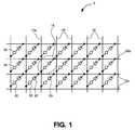
- FIG. 1is a schematic diagram of an array of memory elements according to an embodiment of the invention.
- FIG. 2schematically illustrates a cross-sectional planar side view of a portion of a semiconductor substrate having dielectric trenches formed therein defining a z-direction thickness of a memory cell in accordance with one embodiment of the invention of forming a memory element on a substrate.
- FIG. 3shows the structure of FIG. 2, through the same cross-sectional view, after the introduction of dopants to form an isolation device for a memory element in accordance with one embodiment of the invention.
- FIG. 4shows the structure of FIG. 3 after the introduction of a masking material over the structure in accordance with one embodiment of the invention.
- FIG. 5shows a schematic top view of the structure of FIG. 4 .
- FIG. 6shows the cross-section of the structure of FIG. 4 through line B-B′.
- FIG. 7shows the structure of FIG. 5, through the same cross-sectional view, after the patterning of the x-direction thickness of a memory cell, the introduction of a dopant between the cells, and the introduction of a dielectric material over the structure.
- FIG. 8shows the structure of FIG. 7, through the same cross-sectional view, after the formation of trenches through the dielectric material in accordance with one embodiment of the invention.
- FIG. 9shows the structure of FIG. 8, through the same cross-sectional view, after the introduction of an electrode material over the structure in accordance with one embodiment of the invention.
- FIG. 10shows the structure of FIG. 9, through the same cross-sectional view, after the introduction of a dopant into the electrode material in accordance with one embodiment of the invention.
- FIG. 11shows the structure of FIG. 10, through the same cross-sectional view, after the introduction of a modifying species into a portion of the electrode material in accordance with one embodiment of the invention.
- FIG. 12shows the structure of FIG. 11, through the same cross-sectional view, after the introduction of barrier material over the electrode in accordance with one embodiment of the invention.
- FIG. 13shows the structure of FIG. 12, through the same cross-sectional view, after the introduction of a volume of memory material and second conductors over the structure, in accordance with one embodiment of the invention.
- FIG. 14shows the structure of FIG. 13, through the same cross-sectional view, after the introduction of the dielectric material over the second conductor and a third conductor coupled to the first conductor in accordance with an embodiment of the invention.
- FIG. 15shows the structure of FIG. 12, after the introduction and patterning of a masking material over a portion of the structure according to another embodiment of the invention.
- FIG. 16shows the structure of FIG. 17 after the removal of a portion of dielectric material adjacent the electrode and the introduction of a low ⁇ , dielectric material according to another embodiment of the invention.
- FIG. 17shows the structure of FIG. 12 after the introduction of a low ⁇ dielectric material adjacent the electrode according to still another embodiment of the invention.
- FIG. 18shows a graphical representation of setting and resetting a volume of a phase change memory material in terms of temperature and time.
- the inventiongenerally relates to an apparatus used, in one aspect, as a memory structure.
- the apparatusincludes a contact on a substrate, a dielectric material overlying the contact, and a phase change element, such as a chalcogenide memory element, overlying the dielectric material.
- a heater elementis disposed in the dielectric material and coupled to the contact and the phase change element.
- a portion of the dielectric materialcomprises a thermal conductivity less than silicon dioxide.
- the energy applied to programe.g., set or reset
- a volume of memory materialmay be concentrated at the volume of memory material.
- an improved memory devicee.g., memory element, memory array, etc. with improved programming capabilities is presented.
- the inventionalso relates to a method, including a method of forming a memory element.
- the methodincludes introducing, over a contact formed on a substrate, a dielectric material, a portion of which comprises a thermal conductivity less than silicon dioxide.
- a heater elementis introduced through the dielectric material to the contact and a phase change material is introduced over the dielectric material and the heater element.
- the energy required to modify the phase of a portion of the phase change materialmay be concentrated adjacent the phase change material.
- the energy required to program a memory devicemay be concentrated at the memory material.
- a method of forming an improved memory deviceis presented, including a memory device with improved programming characteristics.
- the embodimentdescribes a memory material including a phase change material wherein the phase of the material determines the state of the memory element.
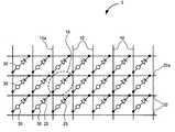
- FIG. 1shows a schematic diagram of an embodiment of a memory array comprised of a plurality of memory elements presented and formed in the context of the invention.
- the circuit of memory array 5includes an xy grid with memory element 30 electrically interconnected in series with isolation device 25 on a portion of a chip.
- Address lines 10e.g., columns
- 20e.g., rows
- One purpose of the xy grid array of memory elements in combination with isolation devicesis to enable each discrete memory element to be read and written without interfering with the information stored in adjacent or remote memory elements of the array.
- a memory array such as memory array 5may be formed in a portion, including the entire portion, of a substrate.
- a typical substrateincludes a semiconductor substrate such as a silicon substrate.
- Other substratesincluding, but not limited to, substrates that contain ceramic material, organic material, or glass material as part of the infrastructure are also suitable.
- memory array 5may be fabricated over an area of the substrate at the wafer level and then the wafer reduced through singulation into discrete die or chips, some or all of the die or chips having a memory array formed thereon. Additional addressing circuitry (e.g., decoders, etc.) may be formed in a similar fashion as known to those of skill in the art.
- FIGS. 2-14illustrate an embodiment of the fabrication of representative memory element 15 of FIG. 1 .
- FIG. 2shows a portion of substrate 100 that is, for example, a semiconductor substrate.
- a P-type dopantsuch as boron is introduced in portion 110 .
- a suitable concentration of P-type dopantis on the order of above 5 ⁇ 10 19 -1 ⁇ 10 20 atoms per cubic centimeters (atoms/cm 3 ) rendering portion 110 of substrate 100 representatively P ++ .
- Overlying portion 110 of substrate 100is portion 120 of P-type epitaxial silicon.
- the dopant concentrationis on the order of about 10 16 -10 17 atoms/cm 3 .
- the introduction and formation of P-type epitaxial silicon portion 120 and P ++ silicon portion 110may follow techniques known to those of skill in the art.
- FIG. 2also shows shallow trench isolation (STI) structures 130 formed in epitaxial portion 120 of substrate 100 .
- STI structures 130serve, in one aspect, to define the z-direction thickness of a memory element cell, with at this point only the z-direction thickness of a memory element cell defined.
- STI structures 130serve to isolate individual memory elements from one another as well as associated circuit elements (e.g., transistor devices) formed in and on the substrate.
- STI structures 130are formed according to techniques known to those skilled in the art.
- FIG. 3shows the structure of FIG. 2 after a further fabrication operation in memory cell regions 135 A and 135 B.
- memory cell regions 135 A and 135 Bare introduced as strips with the x-direction dimension greater than the z-direction dimension.
- first conductor or signal line material 140is N-type doped polysilicon formed by the introduction of, for example, phosphorous or arsenic to a concentration on the order of about 10 18 -10 19 atoms/cm 3 (e.g., N + silicon).
- first conductor or signal line material 140serves as an address line, a row line (e.g., row line 20 of FIG. 1 ).
- first conductor or signal line material 140Overlying first conductor or signal line material 140 is an isolation device (e.g., isolation device 25 of FIG. 1 ).
- the isolation deviceis a PN diode formed of N-type silicon portion 150 (dopant concentration on the order of about 10 17 -10 18 atoms/cm 3 ) and P-type silicon portion 160 (dopant concentration on the order of about 10 19 -10 20 atoms/cm 3 ).
- PN diodeis shown, it is to be appreciated that other isolation structures are similarly suitable.
- Such devicesinclude, but are not limited to, MOS devices.
- reducer material 170of, in this example, a refractory metal silicide such as cobalt silicide (CoSi 2 ).
- Reducer material 170serves as a low resistance material in the fabrication of peripheral circuitry (e.g., addressing circuitry) of the circuit structure on the chip.
- peripheral circuitrye.g., addressing circuitry
- reducer material 170is not required in terms of forming a memory element as described. Nevertheless, because of its low resistance property, its inclusion as part of the memory cell structure between isolation device 25 and memory element 30 is utilized in this embodiment.
- FIG. 4shows the structure of FIG. 3 after the introduction of masking material 180 .
- masking material 180serves, in one sense, as an etch stop for a subsequent etch operation.
- FIG. 5schematically shows memory cell regions 135 A and 135 B in an xz plane. Overlying the memory cell is masking material 180 .
- FIG. 6shows a cross-sectional side view of memory cell region 135 A through line B—B′ of FIG. 5 (i.e., an xy perspective).
- a suitable material for masking material 180is a dielectric material such as silicon nitride (Si 3 N 4 ).
- FIG. 7shows the structure of FIG. 6 (from an xy perspective) after patterning of the x-direction thickness of the memory cell material.
- FIG. 7shows two memory cells 145 A and 145 B patterned from memory cell region 135 A (see FIG. 5 ).
- the patterningmay be accomplished using conventional techniques for etching, in this example, refractory metal silicide and silicon material to the exclusion of masking material 180 (e.g., Si 3 N 4 ).
- the definition of the x-direction thicknessinvolves, in one embodiment, an etch to conductive material 150 of the memory line stack to define memory cells 145 A and 145 B of memory cell region 135 A.
- the etchproceeds through the memory line stack to, in this example, a portion of conductor or signal line material 150 .
- a timed etchmay be utilized to stop an etch at this point.
- N-type dopantis introduced at the base of each trench 190 to form pockets 200 having a dopant concentration on the order of about 10 18 -10 20 atoms/cm 3 (e.g., N + region) between memory cells 145 A and 145 B. Pockets 200 serve, in one sense, to maintain continuity of a row line.
- FIG. 7also shows dielectric material 210 introduced over the structure to a thickness on the order of 100 ⁇ to 50,000 ⁇ .
- dielectric material 210is silicon dioxide (SiO 2 ).
- dielectric material 210is a material selected for its reduced thermal conductivity, ⁇ , preferably a thermal conductivity less than ⁇ SiO 2 , more preferably three to 10 times less ⁇ SiO 2 .
- SiO 2 and silicon nitride (Si 3 N 4 )have ⁇ values on the order of 1.0.
- suitable materials for dielectric material 210include those materials that have ⁇ values less than 1.0.
- Certain high temperature polymershaving ⁇ values less than 1.0, carbide materials, Aerogel, Xerogel ( ⁇ on the order of 0.1) and their derivatives.
- dielectric material 210need not be of a material having a thermal conductivity, ⁇ , less than ⁇ SiO 2 .
- a first potion of dielectric material introduced, for example, in a portion including the entire portion of trench 190 and a portion over dielectric material 180may be a first dielectric of SiO 2 or a material having a thermal conductivity, ⁇ , similar to ⁇ SiO 2 .
- a second portion over the first portionmay then be of a material having a ⁇ , less than ⁇ SiO 2 .
- a portion of dielectric material 210 more proximally adjacent to subsequently introduced memory materialhas a ⁇ less than ⁇ SiO 2 .
- FIGS. 8-13generally describe, among other things, the introduction and of memory material and an electrode between a contact (e.g., first conductor or signal line material 140 ) and the memory material.
- the electrode materialis “edgewise adjacent” to the memory material. That is, only an edge or a portion of an edge of the electrode material is adjacent to the memory material. Substantially all of the remainder of the electrode is remote to the memory material.
- substantially all of the electrical communication between the electrodeis through an edge of the electrode or a portion of an edge. That is, it is preferable that substantially all electrical communication is through at least a portion of an edge (i.e., an “edge portion”) of the electrode.
- the terminology “area of contact”is the portion of the surface of an electrical contact through which the electrical contact electrically communicates with the memory material. As noted, in one embodiment, a substantially all electrical communication between the memory material and the electrode occurs through all or a portion of an edge of the electrode. Hence, the area of contact between the electrode and the memory material is an edge of the electrode or a portion of an edge of the electrode. That is, the area of contact between the electrode and the memory material is an “edge portion” of the electrode. It is again noted that the electrode need not actually physically contact the memory material. It is sufficient that the electrode is in electrical communication with the memory material.
- an objectiveis to reduce the area of contact the electrode to the memory material.
- FIG. 8shows the structure of FIG. 7 after the formation of trenches 220 through dielectric materials 210 and 180 to reducer material 170 .
- the formation of trenches 220may be accomplished using etch patterning with an etchant(s) selective for etching dielectric material 210 and masking material 180 and not reducer material 170 (e.g., reducer 170 serving as an etch stop).
- FIG. 9shows the structure of FIG. 8 after the conformal introduction of electrode material 230 .
- electrode material 230is polycrystalline semiconductor material such as polycrystalline silicon.
- suitable materialsinclude carbon and semi-metals such as transition metals including, but not limited to, titanium, titanium-tungsten (TiW), titanium nitride (TiN) and titanium aluminum nitride (TiAlN).
- TiWtitanium-tungsten
- TiNtitanium nitride
- TiAlNtitanium aluminum nitride
- the introductionis conformal in the sense that electrode material 230 is introduced along the side walls and base of trench 220 such that electrode material 230 is in contact with reducer material 170 .
- the conformal introduction of electrode material 230 that is, for example, polycrystalline siliconmay follow conventional introduction techniques known to those skilled in the art including chemical vapor deposition (CVD) techniques.
- CVDchemical vapor deposition
- the electrode material extending in the figures in a y-directioni.e., only one of two “leg portions” extending in a y-direction, constitutes the area of contact with the subsequently introduced memory material.
- non-conductive material selected for electrode material 230such as intrinsic polycrystalline silicon
- one of the two leg portions of electrode material 230is rendered conductive for a conductive path to first conductor or signal line material 140 .
- the conductivity of the materialmay be increased by doping techniques, by for example angled ion implantation into the desired leg portion.
- an otherwise conductive path between the non-selected leg portion and first conductor or signal line material 140may be terminated by, for example introducing a dielectric material between the electrode material and the memory material or by removing a portion of the electrode material by, for example, etching.
- FIG. 10shows the structure of FIG. 9 where only one of the leg portions of electrode material 230 serves as a conductive path between first conductor or signal line material 140 and a subsequently introduced memory material.
- electrode material 230is a generally non-conductive intrinsic polycrystalline silicon. After the introduction of a dopant into a portion of electrode material 230 , two portions are defined, electrode material 230 A and electrode material 230 B. As illustrated, electrode material 230 A is doped about its length from reducer material 170 and will act as a conductive path between first conductor or signal line material 140 and subsequently introduced memory material. Electrode material 230 B is generally non-conductive (e.g., predominantly intrinsic polycrystalline silicon) and thus will generally not serve as a conductive path.
- FIG. 10also shows the structure after the introduction of dielectric material 250 into trenches 220 .
- dielectric material 250is silicon dioxide (SiO 2 ).
- dielectric material 250is a material that has a thermal conductivity, ⁇ , that is less than the thermal conductivity of SiO 2 , ⁇ SiO 2 preferably three to 10 times less than ⁇ SiO 2 . Materials such as described above with reference to FIG. 7 and the accompanying text (including certain polymers and Xerogel) are suitable. Also, from that referenced discussion, it is to be appreciated that the entire portion of dielectric material 250 need not be of a material having a ⁇ less than ⁇ SiO 2 .
- only that portion of material adjacent a subsequently introduced memory materialhas a ⁇ less than ⁇ SiO 2 .
- the structureis subjected to a planarization that removes the horizontal component of electrode material 230 .
- Suitable planarization techniquesinclude those known to those of skill in the art, such as chemical or chemical-mechanical polish (CMP) techniques.
- dielectric materials 210 or 250are desired to be of a material that has a thermal conductivity, ⁇ , less than ⁇ SiO 2 .
- thatmay be all or a portion of dielectric material 210 , with dielectric material 250 of SiO 2 or a material with a thermal conductivity similar to ⁇ SiO 2 .
- all or a portion of dielectric material 250may be of a material with a thermal conductivity, ⁇ , less than ⁇ SiO 2 , with dielectric material 210 of SiO 2 or a material with a thermal conductivity similar to ⁇ SiO 2 .
- all or a portion of both dielectric material 210 and dielectric material 250may be of a material with a thermal conductivity, ⁇ , less than ⁇ SiO 2 .
- FIG. 11shows the structure of FIG. 10 after the optional introduction of modifying species 260 into a portion of electrode material 230 A.
- modifying species 260is introduced to raise the local resistance of electrode material 230 A at a portion of electrode material 270 defined by length, h 1 .
- Electrode material 270 of polycrystalline silicon and SiO 2 , Si 3 N 4 , Si x O y N z , or SiCgenerally has a higher resistivity than doped polycrystalline silicon of electrode material 230 A.
- Suitable materials for modifying speciesalso include those materials that are introduced (e.g., added, reacted, or combined) into electrode material 230 A and raise the resistivity value within the electrode (e.g., raise the local resistance near a volume of memory material), and the resistivity value is also stable at high temperatures.
- Such modifying speciesmay be introduced by way of implantation or thermal means with, for example, a gaseous ambient.
- FIG. 12shows the structure of FIG. 11 after the optional introduction of barrier materials 270 and 280 .
- Barrier material 270is, for example, titanium silicide (TiSi 2 ) introduced to a thickness on the order of about 100-300 ⁇ .
- Barrier material 280is, for example, titanium nitride (TiN) similarly introduced to a thickness on the order of about 25-300 ⁇ .
- the introduction of barrier materials 270 and 280may be accomplished using techniques known to those skilled in the art.
- FIG. 13shows the structure of FIG. 12 after the introduction of a volume of memory material 290 (represented as memory element 30 in FIG. 1 ).
- memory material 290is a phase change material.
- memory material 290includes a chalcogenide element(s).
- phase change memory material 290include, but are not limited to, compositions of the class of tellerium-germanium-antimony (Te x Ge y Sb z ) material.
- Memory material 290in one example according to current technology, is introduced with a thickness on the order of about 600 ⁇ .
- barrier materials 300 and 310of, for example, titanium (Ti) and titanium nitride (TiN), respectively.
- Barrier materialserves, in one aspect, to inhibit diffusion between the volume of memory material 290 and second conductor or signal line material overlying the volume of memory material 290 (e.g., second electrode 10 ).
- second conductor or signal line material 315Overlying barrier materials 300 and 310 is second conductor or signal line material 315 .
- second conductor or signal line material 315serves as an address line, a column line (e.g., column line 10 of FIG. 1 ).
- Second conductor or signal line material 315is patterned to be, in one embodiment, generally orthogonal to first conductor or signal line material 140 (column lines are orthogonal to row lines). Second conductor or signal line material 315 is, for example, an aluminum material, such as an aluminum alloy. Methods for the introduction and patterning of the barrier materials and second conductor or signal line material 315 include such techniques as known to those of skill in the art. It is to be appreciated at this point that memory material 290 may be patterned contiguously with second conductor or signal line material 315 such that memory material 290 is itself strips (like second conductor or signal line material 315 ) or is in a cellular form (achieved by patterning prior to patterning second conductor or signal line material 315 ).
- FIG. 14shows the structure of FIG. 13 after the introduction of dielectric material 330 over second conductor or signal line material 315 .
- Dielectric material 330is, for example, SiO 2 or other suitable material that surrounds second conductor or signal line material 315 and memory material 290 to electronically isolate such structure.
- dielectric material 330is planarized and a via is formed in a portion of the structure through dielectric material 330 , dielectric material 210 , and masking material 180 to reducer material 170 .
- the viais filled with conductive material 340 such as tungsten (W) and barrier material 350 such as a combination of titanium (Ti) and titanium nitride (TiN).
- conductive material 340such as tungsten (W)
- barrier material 350such as a combination of titanium (Ti) and titanium nitride (TiN).
- the structure shown in FIG. 14also shows additional conductor or signal line material 320 introduced and patterned to mirror that of first conductor or signal line material 140 (e.g., row line) formed on substrate 100 .
- Mirror conductor line material 320mirrors first conductor or signal line material 140 and is coupled to first conductor or signal line material 140 through a conductive via.
- mirror conductor line material 320serves, in one aspect, to reduce the resistance of conductor or signal line material 140 in a memory array, such as memory array 5 illustrated in FIG. 1.
- a suitable material for mirror conductor line material 320includes an aluminum material, such as an aluminum alloy.
- the electrodedelivers electrical current to the memory material.
- the electrical currentpasses through the electrode and through the memory material, at least a portion of the electric potential energy of the electrons is transferred to the surrounding material as heat. That is, the electrical energy is converted to heat energy via Joule heating.
- the amount of electrical energy converted to heat energyincreases with the resistivity of the material as well as with the current density passing through the material.
- dissipating power in the electrical contact from Joule heating adjacent to the memory materialmay at least partially assist (or may even dominate) the programming of the memory material. It is also believed that dissipating power in the electrical contact remote to the memory material may actually waste power and increase the total energy needed to program the memory material.
- providing an electrical contact structure having a relatively high power dissipation adjacent to the memory material and a relatively low power dissipation remote to the memory materialmay thus decrease the total power and energy needed to program the memory device.
- providing a dielectric material having a ⁇ less than ⁇ SiO 2decreases the total power and energy needed to program the memory device.
- memory elements of memory array 5may be fabricated in the same manner. It is to be appreciated that many, and possibly all, memory elements of memory array 5 , along with other integrated circuit circuitry, may be fabricated simultaneously.
- FIG. 15shows the structure after the introduction of masking material 370 over the structure to define an opening over the conductive portion of an electrode material (e.g., similar in area to the area occupied over the structure by a subsequently introduced memory material 290 ).
- Suitable masking materialsare known to those of skill in the art and include photoimageable materials.
- dielectric material 210 and dielectric material 250are selectively etched (at the exclusion of the electrode material) to a desired depth.
- a suitable etch chemistry for etching SiO 2 in the presence and to the exclusion of polycrystalline siliconis a gaseous hydrobromic acid and chlorine chemistry.
- One desired depth according to current technologiesis approximately 600 ⁇ (similar to the depth of electrode material 270 ).
- masking material 370is removed, and dielectric material 380 having a thermal conductivity, ⁇ , less than ⁇ SiO 2 , preferably three to 10 times less than ⁇ SiO 2 , is introduced as shown in FIG. 16 .
- the materialmay be introduced by a spinning process. Following introduction, the Xerogel may be cured. A planarization may then be used, such as a CMP, to planarize the structure to a desired structure height. The process then proceeds as described above with reference to FIG. 13 and FIG. 14 and the accompanying text.
- the entire portion of dielectric material 250is a material having a ⁇ less than ⁇ SiO 2
- a portion of dielectric material 210 , adjacent electrode material 230 Ais a material with ⁇ less than ⁇ SiO 2 while the remainder of dielectric material 210 is SiO 2 or a material having a ⁇ similar to ⁇ SiO 2
- dielectric portion 380formed for example by selective etching similar to the technique described with reference to FIGS. 15 and 16, is a dielectric material having a ⁇ less than ⁇ SiO 2 .
- Electrode material 230 Athere may be a right side, left side, front side, and back side to electrode material 230 A, particularly to an active electrode area generally desired, as described above, to be adjacent memory material 290 .
- the low ⁇ dielectric materiale.g., ⁇ less than ⁇ SiO 2
- FIG. 18presents a graphical representation of the programming (e.g., setting and resetting) of a volume of phase change memory material.
- programming memory element 15(addressed by column line 10 a and row line 20 a ) involves, in one example, supplying a voltage to column line 10 a to introduce a current into the volume of memory material 30 . The current causes a temperature increase at the volume of memory material 30 .
- T Me.g., beyond the melting point of the memory material.
- a representative amorphizing temperature for a Te x Ge y Sb 2 materialis on the order of about 600-650° C.
- the volume of memory material 30was heated to a high temperature to amorphisize the material and reset the memory element (e.g., program 0 ). Heating the volume of memory material to a lower crystallization temperature crystallizes the material and sets the memory element (e.g., program 1 ). It is to be appreciated that the association of reset and set with amorphous and crystalline material, respectively, is a convention and that at least an opposite convention may be adopted. It is also to be appreciated from this example that the volume of memory material 30 need not be partially set or reset by varying the current flow and duration through the volume of memory material.
Landscapes
- Chemical & Material Sciences (AREA)
- Crystallography & Structural Chemistry (AREA)
- Engineering & Computer Science (AREA)
- Manufacturing & Machinery (AREA)
- Semiconductor Memories (AREA)
Abstract
Description
Claims (22)
Priority Applications (3)
| Application Number | Priority Date | Filing Date | Title |
|---|---|---|---|
| US09/676,317US6339544B1 (en) | 2000-09-29 | 2000-09-29 | Method to enhance performance of thermal resistor device |
| US09/944,349US6621095B2 (en) | 2000-09-29 | 2001-08-29 | Method to enhance performance of thermal resistor device |
| US10/611,600US6770524B2 (en) | 2000-09-29 | 2003-07-01 | Method to enhance performance of thermal resistor device |
Applications Claiming Priority (1)
| Application Number | Priority Date | Filing Date | Title |
|---|---|---|---|
| US09/676,317US6339544B1 (en) | 2000-09-29 | 2000-09-29 | Method to enhance performance of thermal resistor device |
Related Child Applications (1)
| Application Number | Title | Priority Date | Filing Date |
|---|---|---|---|
| US09/944,349ContinuationUS6621095B2 (en) | 2000-09-29 | 2001-08-29 | Method to enhance performance of thermal resistor device |
Publications (1)
| Publication Number | Publication Date |
|---|---|
| US6339544B1true US6339544B1 (en) | 2002-01-15 |
Family
ID=24714045
Family Applications (3)
| Application Number | Title | Priority Date | Filing Date |
|---|---|---|---|
| US09/676,317Expired - LifetimeUS6339544B1 (en) | 2000-09-29 | 2000-09-29 | Method to enhance performance of thermal resistor device |
| US09/944,349Expired - LifetimeUS6621095B2 (en) | 2000-09-29 | 2001-08-29 | Method to enhance performance of thermal resistor device |
| US10/611,600Expired - LifetimeUS6770524B2 (en) | 2000-09-29 | 2003-07-01 | Method to enhance performance of thermal resistor device |
Family Applications After (2)
| Application Number | Title | Priority Date | Filing Date |
|---|---|---|---|
| US09/944,349Expired - LifetimeUS6621095B2 (en) | 2000-09-29 | 2001-08-29 | Method to enhance performance of thermal resistor device |
| US10/611,600Expired - LifetimeUS6770524B2 (en) | 2000-09-29 | 2003-07-01 | Method to enhance performance of thermal resistor device |
Country Status (1)
| Country | Link |
|---|---|
| US (3) | US6339544B1 (en) |
Cited By (282)
| Publication number | Priority date | Publication date | Assignee | Title |
|---|---|---|---|---|
| US20020116955A1 (en)* | 2001-02-19 | 2002-08-29 | Sumitomo Electric Industries, Ltd. | Method of forming soot preform |
| US20020168852A1 (en)* | 2001-05-11 | 2002-11-14 | Harshfield Steven T. | PCRAM memory cell and method of making same |
| US6487113B1 (en)* | 2001-06-29 | 2002-11-26 | Ovonyx, Inc. | Programming a phase-change memory with slow quench time |
| US20030045049A1 (en)* | 2001-08-29 | 2003-03-06 | Campbell Kristy A. | Method of forming chalcogenide comprising devices |
| US20030047772A1 (en)* | 2001-03-15 | 2003-03-13 | Jiutao Li | Agglomeration elimination for metal sputter deposition of chalcogenides |
| US6534781B2 (en)* | 2000-12-26 | 2003-03-18 | Ovonyx, Inc. | Phase-change memory bipolar array utilizing a single shallow trench isolation for creating an individual active area region for two memory array elements and one bipolar base contact |
| US20030082908A1 (en)* | 2001-10-30 | 2003-05-01 | Lowrey Tyler A. | Phase change material memory device |
| US20030090922A1 (en)* | 2000-09-29 | 2003-05-15 | Lowrey Tyler A. | Single level metal memory cell using chalcogenide cladding |
| US20030096497A1 (en)* | 2001-11-19 | 2003-05-22 | Micron Technology, Inc. | Electrode structure for use in an integrated circuit |
| US20030117831A1 (en)* | 2001-12-20 | 2003-06-26 | Glen Hush | Programmable conductor random access memory and a method for writing thereto |
| US20030128612A1 (en)* | 2002-01-04 | 2003-07-10 | John Moore | PCRAM rewrite prevention |
| US6597031B2 (en)* | 2001-12-18 | 2003-07-22 | Mitsubishi Denki Kabushiki Kaisha | Ovonic unified memory device and magnetic random access memory device |
| US6597009B2 (en)* | 2000-09-29 | 2003-07-22 | Intel Corporation | Reduced contact area of sidewall conductor |
| US20030156463A1 (en)* | 2002-02-19 | 2003-08-21 | Casper Stephen L. | Programmable conductor random access memory and method for sensing same |
| US20030156468A1 (en)* | 2002-02-20 | 2003-08-21 | Campbell Kristy A. | Resistance variable 'on' memory |
| US20030155606A1 (en)* | 2002-02-15 | 2003-08-21 | Campbell Kristy A. | Method to alter chalcogenide glass for improved switching characteristics |
| WO2003073512A1 (en)* | 2002-02-22 | 2003-09-04 | Ovonyx, Inc. | Single level metal memory cell using chalcogenide cladding |
| WO2003073511A1 (en)* | 2002-02-22 | 2003-09-04 | Intel Corporation | Dual trench isolation for a phase-change memory cell and method of making same |
| US20030169625A1 (en)* | 2002-03-05 | 2003-09-11 | Glen Hush | Programmable conductor random access memory and method for sensing same |
| US20030173558A1 (en)* | 2002-03-14 | 2003-09-18 | Campbell Kristy A. | Methods and apparatus for resistance variable material cells |
| US20030193059A1 (en)* | 2002-04-10 | 2003-10-16 | Gilton Terry L. | Programmable conductor memory cell structure and method therefor |
| US20030194865A1 (en)* | 2002-04-10 | 2003-10-16 | Gilton Terry L. | Method of manufacture of programmable conductor memory |
| US20030193053A1 (en)* | 2002-04-10 | 2003-10-16 | Gilton Terry L. | Thin film diode integrated with chalcogenide memory cell |
| US20030193063A1 (en)* | 2000-12-21 | 2003-10-16 | Chien Chiang | Metal structure for a phase-change memory device |
| US20030203555A1 (en)* | 2001-06-30 | 2003-10-30 | Dennison Charles H. | Reduced area intersection between electrode and programming element |
| US20030218904A1 (en)* | 2001-06-29 | 2003-11-27 | Lowrey Tyler A. | Programming a phase-change material memory |
| EP1376604A1 (en)* | 2002-06-21 | 2004-01-02 | Hewlett-Packard Development Company, L.P. | Memory structures |
| US20040007749A1 (en)* | 2002-07-10 | 2004-01-15 | Campbell Kristy A. | Assemblies displaying differential negative resistance |
| US20040007718A1 (en)* | 2001-08-30 | 2004-01-15 | Campbell Kristy A. | Stoichiometry for chalcogenide glasses useful for memory devices and method of formation |
| US20040029351A1 (en)* | 2002-01-31 | 2004-02-12 | Gilton Terry L. | Methods of forming non-volatile resistance variable devices and methods of forming silver selenide comprising structures |
| US20040038480A1 (en)* | 2002-08-22 | 2004-02-26 | Moore John T. | Method of manufacture of a PCRAM memory cell |
| US20040043553A1 (en)* | 2002-06-06 | 2004-03-04 | Jiutao Li | Elimination of dendrite formation during metal/chalcogenide glass deposition |
| US20040040835A1 (en)* | 2002-08-29 | 2004-03-04 | Jiutao Li | Silver selenide film stoichiometry and morphology control in sputter deposition |
| US20040043245A1 (en)* | 2002-08-29 | 2004-03-04 | Moore John T. | Method to control silver concentration in a resistance variable memory element |
| US20040053461A1 (en)* | 2002-08-29 | 2004-03-18 | Moore John T. | Graded GexSe100-x concentration in PCRAM |
| US20040051094A1 (en)* | 2002-09-13 | 2004-03-18 | Mitsubishi Denki Kabushiki Kaisha | Non-volatile semiconductor memory device allowing shrinking of memory cell |
| US6731535B1 (en) | 2002-12-10 | 2004-05-04 | Renesas Technology Corp. | Nonvolatile semiconductor memory device |
| US20040115372A1 (en)* | 2002-12-13 | 2004-06-17 | Tyler Lowrey | Vertical elevated pore phase change memory |
| US20040114317A1 (en)* | 2002-12-13 | 2004-06-17 | Chien Chiang | Forming phase change memories |
| EP1431982A1 (en)* | 2002-09-26 | 2004-06-23 | Sharp Kabushiki Kaisha | Method of fabricating 1T1R resistive memory array |
| US20040124406A1 (en)* | 2001-08-29 | 2004-07-01 | Campbell Kristy A. | Method of forming non-volatile resistance variable devices, method of forming a programmable memory cell of memory circuitry, and a non-volatile resistance variable device |
| US20040130598A1 (en)* | 2002-07-10 | 2004-07-08 | Canon Kabushiki Kaisha | Ink jet record head |
| US20040157417A1 (en)* | 2002-08-29 | 2004-08-12 | Moore John T. | Methods to form a memory cell with metal-rich metal chalcogenide |
| US20040161874A1 (en)* | 2001-03-01 | 2004-08-19 | Moore John T. | Method of forming a non-volatile resistance variable device, and non-volatile resistance variable device |
| US20040166604A1 (en)* | 2003-02-25 | 2004-08-26 | Samsung Electronics Co. Ltd. | Phase changeable memory cells and methods of fabricating the same |
| US20040175859A1 (en)* | 2002-08-29 | 2004-09-09 | Campbell Kristy A. | Single polarity programming of a PCRAM structure |
| US20040180533A1 (en)* | 2003-03-14 | 2004-09-16 | Li Li | Method for filling via with metal |
| US20040192006A1 (en)* | 2002-02-20 | 2004-09-30 | Campbell Kristy A. | Layered resistance variable memory device and method of fabrication |
| US20040202016A1 (en)* | 2003-04-10 | 2004-10-14 | Campbell Kristy A. | Differential negative resistance memory |
| US6809362B2 (en) | 2002-02-20 | 2004-10-26 | Micron Technology, Inc. | Multiple data state memory cell |
| US20040211957A1 (en)* | 2002-08-29 | 2004-10-28 | Moore John T. | Method and apparatus for controlling metal doping of a chalcogenide memory element |
| US6813178B2 (en) | 2003-03-12 | 2004-11-02 | Micron Technology, Inc. | Chalcogenide glass constant current device, and its method of fabrication and operation |
| US20040235235A1 (en)* | 2002-06-06 | 2004-11-25 | Jiutao Li | Co-sputter deposition of metal-doped chalcogenides |
| US6833559B2 (en) | 2001-02-08 | 2004-12-21 | Micron Technology, Inc. | Non-volatile resistance variable device |
| US20040264234A1 (en)* | 2003-06-25 | 2004-12-30 | Moore John T. | PCRAM cell operation method to control on/off resistance variation |
| US20050018509A1 (en)* | 2001-11-20 | 2005-01-27 | Glen Hush | Complementary bit resistance memory sensor and method of operation |
| US20050017233A1 (en)* | 2003-07-21 | 2005-01-27 | Campbell Kristy A. | Performance PCRAM cell |
| US20050026433A1 (en)* | 2001-08-30 | 2005-02-03 | Jiutao Li | Integrated circuit device and fabrication using metal-doped chalcogenide materials |
| US20050054207A1 (en)* | 2002-08-29 | 2005-03-10 | Micron Technology, Inc. | Plasma etching methods and methods of forming memory devices comprising a chalcogenide comprising layer received operably proximate conductive electrodes |
| US20050059187A1 (en)* | 2003-09-17 | 2005-03-17 | Gilton Terry L. | Non-volatile memory structure |
| US20050062074A1 (en)* | 2002-08-09 | 2005-03-24 | Macronix International Co., Ltd. | Spacer chalcogenide memory method |
| US6894304B2 (en) | 2001-08-27 | 2005-05-17 | Micron Technology, Inc. | Apparatus and method for dual cell common electrode PCRAM memory device |
| US20050104146A1 (en)* | 2003-11-14 | 2005-05-19 | Nickel Janice H. | Thin film device and a method of providing thermal assistance therein |
| US20050162907A1 (en)* | 2004-01-28 | 2005-07-28 | Campbell Kristy A. | Resistance variable memory elements based on polarized silver-selenide network growth |
| US20050162883A1 (en)* | 2002-08-08 | 2005-07-28 | Hasan Nejad | Columnar 1T-nMemory cell structure and its method of formation and operation |
| US20050167689A1 (en)* | 2004-01-29 | 2005-08-04 | Campbell Kristy A. | Non-volatile zero field splitting resonance memory |
| US20050174828A1 (en)* | 2004-02-11 | 2005-08-11 | Manish Sharma | Switching of MRAM devices having soft magnetic reference layers |
| US20050201174A1 (en)* | 2004-03-10 | 2005-09-15 | Klein Dean A. | Power management control and controlling memory refresh operations |
| US20050202588A1 (en)* | 2004-03-10 | 2005-09-15 | Brooks Joseph F. | Method of forming a chalcogenide material containing device |
| US6951805B2 (en) | 2001-08-01 | 2005-10-04 | Micron Technology, Inc. | Method of forming integrated circuitry, method of forming memory circuitry, and method of forming random access memory circuitry |
| US6961277B2 (en) | 2003-07-08 | 2005-11-01 | Micron Technology, Inc. | Method of refreshing a PCRAM memory device |
| US20060012008A1 (en)* | 2004-07-19 | 2006-01-19 | Campbell Kristy A | Resistance variable memory device and method of fabrication |
| US20060011910A1 (en)* | 2004-07-19 | 2006-01-19 | Micron Technology, Inc. | PCRAM device with switching glass layer |
| US20060035403A1 (en)* | 2004-08-12 | 2006-02-16 | Campbell Kristy A | PCRAM device with switching glass layer |
| US20060033094A1 (en)* | 2004-08-12 | 2006-02-16 | Campbell Kristy A | Resistance variable memory with temperature tolerant materials |
| US20060044906A1 (en)* | 2004-09-01 | 2006-03-02 | Ethan Williford | Sensing of resistance variable memory devices |
| US7010644B2 (en) | 2002-08-29 | 2006-03-07 | Micron Technology, Inc. | Software refreshed memory device and method |
| US20060073631A1 (en)* | 2004-09-24 | 2006-04-06 | Karpov Ilya V | Phase change memory with damascene memory element |
| US20060077706A1 (en)* | 2004-10-08 | 2006-04-13 | Chien-Ming Li | Multilevel phase-change memory, operating method and manufacture method thereof |
| US20060084227A1 (en)* | 2004-10-14 | 2006-04-20 | Paola Besana | Increasing adherence of dielectrics to phase change materials |
| US20060110878A1 (en)* | 2004-11-22 | 2006-05-25 | Macronix International Co., Ltd. | Side wall active pin memory and manufacturing method |
| US20060124916A1 (en)* | 2004-12-09 | 2006-06-15 | Macronix International Co., Ltd. | Self-aligned small contact phase-change memory method and device |
| US20060131555A1 (en)* | 2004-12-22 | 2006-06-22 | Micron Technology, Inc. | Resistance variable devices with controllable channels |
| US20060131556A1 (en)* | 2004-12-22 | 2006-06-22 | Micron Technology, Inc. | Small electrode for resistance variable devices |
| US20060148125A1 (en)* | 2003-03-21 | 2006-07-06 | Hideki Horii | Phase changable memory device structures |
| US20060163554A1 (en)* | 2002-10-11 | 2006-07-27 | Koninklijke Philips Electronics N.C. | Electric device comprising phase change material |
| US20060175596A1 (en)* | 2005-02-10 | 2006-08-10 | Thomas Happ | Phase change memory cell with high read margin at low power operation |
| US20060203541A1 (en)* | 2003-03-18 | 2006-09-14 | Haruki Toda | Phase change memory device |
| US20060237707A1 (en)* | 2005-04-22 | 2006-10-26 | Micron Technology, Inc. | Memory array for increased bit density and method of forming the same |
| US20060256640A1 (en)* | 2005-05-16 | 2006-11-16 | Micron Technology, Inc. | Power circuits for reducing a number of power supply voltage taps required for sensing a resistive memory |
| US20060270099A1 (en)* | 2001-08-29 | 2006-11-30 | Micron Technology, Inc. | Method of forming non-volatile resistance variable devices and method of forming a programmable memory cell of memory circuitry |
| US20060284214A1 (en)* | 2005-06-17 | 2006-12-21 | Macronix International Co., Ltd. | Thin film fuse phase change cell with thermal isolation layer and manufacturing method |
| US20060286709A1 (en)* | 2005-06-17 | 2006-12-21 | Macronix International Co., Ltd. | Manufacturing methods for thin film fuse phase change ram |
| US20060286743A1 (en)* | 2005-06-17 | 2006-12-21 | Macronix International Co., Ltd. | Method for Manufacturing a Narrow Structure on an Integrated Circuit |
| US20060284157A1 (en)* | 2005-06-17 | 2006-12-21 | Macronix International Co., Ltd. | Thin film plate phase change RAM circuit and manufacturing method |
| US20060284158A1 (en)* | 2005-06-17 | 2006-12-21 | Macronix International Co., Ltd. | Self-aligned, embedded phase change ram and manufacturing method |
| US20060284279A1 (en)* | 2005-06-17 | 2006-12-21 | Macronix International Co., Ltd. | Thin film fuse phase change RAM and manufacturing method |
| US20070007506A1 (en)* | 2002-02-20 | 2007-01-11 | Micron Technology, Inc. | Layered resistance variable memory device and method of fabrication |
| US20070008768A1 (en)* | 2005-07-08 | 2007-01-11 | Micron Technology, Inc. | Process for erasing chalcogenide variable resistance memory bits |
| US20070023744A1 (en)* | 2005-08-01 | 2007-02-01 | Micron Technology, Inc. | Resistance variable memory device with sputtered metal-chalcogenide region and method of fabrication |
| US20070030554A1 (en)* | 2005-08-02 | 2007-02-08 | Micron Technology, Inc. | Method and apparatus for providing color changing thin film material |
| US20070029537A1 (en)* | 2005-08-02 | 2007-02-08 | Micron Technology, Inc. | Phase change memory cell and method of formation |
| US20070034921A1 (en)* | 2005-08-09 | 2007-02-15 | Micron Technology, Inc. | Access transistor for memory device |
| US20070037316A1 (en)* | 2005-08-09 | 2007-02-15 | Micron Technology, Inc. | Memory cell contact using spacers |
| US20070035990A1 (en)* | 2005-08-15 | 2007-02-15 | Micron Technology, Inc. | Method and apparatus providing a cross-point memory array using a variable resistance memory cell and capacitance |
| US20070047297A1 (en)* | 2005-08-31 | 2007-03-01 | Campbell Kristy A | Resistance variable memory element with threshold device and method of forming the same |
| US20070059882A1 (en)* | 2005-04-22 | 2007-03-15 | Micron Technology, Inc. | Memory elements having patterned electrodes and method of forming the same |
| US20070090354A1 (en)* | 2005-08-11 | 2007-04-26 | Micron Technology, Inc. | Chalcogenide-based electrokinetic memory element and method of forming the same |
| US20070109836A1 (en)* | 2005-11-15 | 2007-05-17 | Macronix International Co., Ltd. | Thermally insulated phase change memory device and manufacturing method |
| US20070109843A1 (en)* | 2005-11-15 | 2007-05-17 | Macronix International Co., Ltd. | Phase Change Memory Device and Manufacturing Method |
| US20070108429A1 (en)* | 2005-11-14 | 2007-05-17 | Macronix International Co., Ltd. | Pipe shaped phase change memory |
| US20070111429A1 (en)* | 2005-11-14 | 2007-05-17 | Macronix International Co., Ltd. | Method of manufacturing a pipe shaped phase change memory |
| US20070121363A1 (en)* | 2005-11-28 | 2007-05-31 | Macronix International Co., Ltd. | Phase Change Memory Cell and Manufacturing Method |
| US20070126040A1 (en)* | 2005-11-21 | 2007-06-07 | Hsiang-Lan Lung | Vacuum cell thermal isolation for a phase change memory device |
| US20070131922A1 (en)* | 2005-12-13 | 2007-06-14 | Macronix International Co., Ltd. | Thin Film Fuse Phase Change Cell with Thermal Isolation Pad and Manufacturing Method |
| US20070131980A1 (en)* | 2005-11-21 | 2007-06-14 | Lung Hsiang L | Vacuum jacket for phase change memory element |
| US20070155172A1 (en)* | 2005-12-05 | 2007-07-05 | Macronix International Co., Ltd. | Manufacturing Method for Phase Change RAM with Electrode Layer Process |
| US20070154847A1 (en)* | 2005-12-30 | 2007-07-05 | Macronix International Co., Ltd. | Chalcogenide layer etching method |
| US20070161186A1 (en)* | 2006-01-09 | 2007-07-12 | Macronix International Co., Ltd. | Programmable Resistive RAM and Manufacturing Method |
| US20070158645A1 (en)* | 2006-01-11 | 2007-07-12 | Macronix International Co., Ltd. | Self-align planerized bottom electrode phase change memory and manufacturing method |
| US20070158690A1 (en)* | 2006-01-09 | 2007-07-12 | Macronix International Co., Ltd. | Programmable Resistive RAM and Manufacturing Method |
| US20070158862A1 (en)* | 2005-11-21 | 2007-07-12 | Hsiang-Lan Lung | Vacuum jacketed electrode for phase change memory element |
| US20070158633A1 (en)* | 2005-12-27 | 2007-07-12 | Macronix International Co., Ltd. | Method for Forming Self-Aligned Thermal Isolation Cell for a Variable Resistance Memory Array |
| US20070158632A1 (en)* | 2006-01-09 | 2007-07-12 | Macronix International Co., Ltd. | Method for Fabricating a Pillar-Shaped Phase Change Memory Element |
| US20070173063A1 (en)* | 2006-01-24 | 2007-07-26 | Macronix International Co., Ltd. | Self-aligned manufacturing method, and manufacturing method for thin film fuse phase change ram |
| US20070173019A1 (en)* | 2006-01-09 | 2007-07-26 | Macronix International Co., Ltd. | Programmable Resistive Ram and Manufacturing Method |
| US20070176261A1 (en)* | 2006-01-30 | 2007-08-02 | Macronix International Co., Ltd. | Vertical Side Wall Active Pin Structures in a Phase Change Memory and Manufacturing Methods |
| US7269044B2 (en) | 2005-04-22 | 2007-09-11 | Micron Technology, Inc. | Method and apparatus for accessing a memory array |
| US20070241371A1 (en)* | 2006-04-17 | 2007-10-18 | Macronix International Co., Ltd. | Memory device and manufacturing method |
| US20070257300A1 (en)* | 2006-05-05 | 2007-11-08 | Macronix International Co., Ltd. | Structures and Methods of a Bistable Resistive Random Access Memory |
| US7294527B2 (en) | 2002-08-29 | 2007-11-13 | Micron Technology Inc. | Method of forming a memory cell |
| US20070262388A1 (en)* | 2006-05-09 | 2007-11-15 | Macronix International Co., Ltd. | Bridge Resistance Random Access Memory Device and Method With A Singular Contact Structure |
| US20070278529A1 (en)* | 2006-05-30 | 2007-12-06 | Macronix International Co., Ltd. | Resistor random access memory cell with l-shaped electrode |
| US20070281420A1 (en)* | 2006-05-30 | 2007-12-06 | Macronix International Co., Ltd. | Resistor random access memory cell with reduced active area and reduced contact areas |
| US20070285971A1 (en)* | 2003-03-18 | 2007-12-13 | Kabushiki Kaisha Toshiba | Resistance change memory device |
| US20070285970A1 (en)* | 2003-03-18 | 2007-12-13 | Kabushiki Kaisha Toshiba | Resistance change memory device |
| US20070285969A1 (en)* | 2003-03-18 | 2007-12-13 | Kabushiki Kaisha Toshiba | Resistance change memory device |
| CN100356567C (en)* | 2004-08-13 | 2007-12-19 | 中国科学院上海微系统与信息技术研究所 | Phase transformation micro, nano electronic memory device and manufacturing method |
| US20080002456A1 (en)* | 2002-04-04 | 2008-01-03 | Kabushiki Kaisha Toshiba | Resistance change memory device |
| US20080002457A1 (en)* | 2002-04-04 | 2008-01-03 | Kabushiki Kaisha Toshiba | Resistance change memory device |
| US20080002455A1 (en)* | 2002-04-04 | 2008-01-03 | Kabushiki Kaisha Toshiba | Resistance change memory device |
| US7317200B2 (en) | 2005-02-23 | 2008-01-08 | Micron Technology, Inc. | SnSe-based limited reprogrammable cell |
| US20080014676A1 (en)* | 2006-07-12 | 2008-01-17 | Macronix International Co., Ltd. | Method for Making a Pillar-Type Phase Change Memory Element |
| US20080043520A1 (en)* | 2006-02-07 | 2008-02-21 | Chen Shih H | I-shaped phase change memory cell with thermal isolation |
| US20080061341A1 (en)* | 2006-09-11 | 2008-03-13 | Macronix International Co., Ltd. | Memory Device Having Wide Area Phase Change Element and Small Electrode Contact Area |
| US20080096375A1 (en)* | 2006-10-18 | 2008-04-24 | Macronix International Co., Ltd. | Method for Making Memory Cell Device |
| US20080094885A1 (en)* | 2006-10-24 | 2008-04-24 | Macronix International Co., Ltd. | Bistable Resistance Random Access Memory Structures with Multiple Memory Layers and Multilevel Memory States |
| US20080096341A1 (en)* | 2006-10-24 | 2008-04-24 | Macronix International Co., Ltd. | Method for Manufacturing a Resistor Random Access Memory with Reduced Active Area and Reduced Contact Areas |
| US20080099791A1 (en)* | 2006-10-04 | 2008-05-01 | Macronix International Co., Ltd. | Memory Cell Device with Circumferentially-Extending Memory Element |
| US20080106923A1 (en)* | 2006-10-24 | 2008-05-08 | Macronix International Co., Ltd. | Phase Change Memory Cells with Dual Access Devices |
| US20080116440A1 (en)* | 2006-11-16 | 2008-05-22 | Macronix International Co., Ltd. | Resistance Random Access Memory Structure for Enhanced Retention |
| US20080121861A1 (en)* | 2006-08-16 | 2008-05-29 | Macronix International Co., Ltd. | Self-Aligned Structure and Method for Confining a Melting Point in a Resistor Random Access Memory |
| US20080135824A1 (en)* | 2006-12-07 | 2008-06-12 | Macronix International Co., Ltd. | Method and Structure of a Multi-Level Cell Resistance Random Access Memory with Metal Oxides |
| US20080138929A1 (en)* | 2006-12-06 | 2008-06-12 | Macronix International Co., Ltd. | Method for Making a Self-Converged Memory Material Element for Memory Cell |
| US20080138931A1 (en)* | 2006-12-06 | 2008-06-12 | Macronix International Co., Ltd. | Method for Making a Self-Converged Void and Bottom Electrode for Memoery Cell |
| US20080137400A1 (en)* | 2006-12-06 | 2008-06-12 | Macronix International Co., Ltd. | Phase Change Memory Cell with Thermal Barrier and Method for Fabricating the Same |
| US7388771B2 (en) | 2006-10-24 | 2008-06-17 | Macronix International Co., Ltd. | Methods of operating a bistable resistance random access memory with multiple memory layers and multilevel memory states |
| US20080142984A1 (en)* | 2006-12-15 | 2008-06-19 | Macronix International Co., Ltd. | Multi-Layer Electrode Structure |
| US20080144353A1 (en)* | 2006-12-13 | 2008-06-19 | Macronix International Co., Ltd. | Method, Apparatus and Computer Program Product for Read Before Programming Process on Programmable Resistive Memory Cell |
| US20080157053A1 (en)* | 2006-12-28 | 2008-07-03 | Macronix International Co., Ltd. | Resistor Random Access Memory Cell Device |
| CN100401547C (en)* | 2002-12-19 | 2008-07-09 | Nxp股份有限公司 | Electronic device with phase change material and method of manufacturing the same |
| US20080165570A1 (en)* | 2007-01-05 | 2008-07-10 | Macronix International Co., Ltd. | Current Compliant Sensing Architecture for Multilevel Phase Change Memory |
| US20080186755A1 (en)* | 2007-02-05 | 2008-08-07 | Macronix International Co., Ltd. | Memory cell device and programming methods |
| US20080186761A1 (en)* | 2007-02-07 | 2008-08-07 | Macronix International Co., Ltd. | Memory Cell with Separate Read and Program Paths |
| US20080185730A1 (en)* | 2007-02-02 | 2008-08-07 | Macronix International Co., Ltd. | Memory cell device with coplanar electrode surface and method |
| US20080191186A1 (en)* | 2007-02-14 | 2008-08-14 | Macronix International Co., Ltd. | Phase change memory cell with filled sidewall memory element and method for fabricating the same |
| US20080192534A1 (en)* | 2007-02-08 | 2008-08-14 | Macronix International Co., Ltd. | Memory element with reduced-current phase change element |
| US20080191187A1 (en)* | 2007-02-12 | 2008-08-14 | Macronix International Co., Ltd. | Method for manufacturing a phase change memory device with pillar bottom electrode |
| US7414258B2 (en) | 2005-11-16 | 2008-08-19 | Macronix International Co., Ltd. | Spacer electrode small pin phase change memory RAM and manufacturing method |
| US20080197333A1 (en)* | 2007-02-21 | 2008-08-21 | Macronix International Co., Ltd. | Programmable Resistive Memory Cell with Self-Forming Gap |
| US20080197334A1 (en)* | 2007-02-21 | 2008-08-21 | Macronix International Co., Ltd. | Phase Change Memory Cell with Heater and Method for Fabricating the Same |
| US20080203375A1 (en)* | 2007-02-27 | 2008-08-28 | Macronix International Co., Ltd. | Memory Cell with Memory Element Contacting Ring-Shaped Upper End of Bottom Electrode |
| US7423300B2 (en) | 2006-05-24 | 2008-09-09 | Macronix International Co., Ltd. | Single-mask phase change memory element |
| US7433226B2 (en) | 2007-01-09 | 2008-10-07 | Macronix International Co., Ltd. | Method, apparatus and computer program product for read before programming process on multiple programmable resistive memory cell |
| US7440315B2 (en) | 2007-01-09 | 2008-10-21 | Macronix International Co., Ltd. | Method, apparatus and computer program product for stepped reset programming process on programmable resistive memory cell |
| US20080258126A1 (en)* | 2007-04-17 | 2008-10-23 | Macronix International Co., Ltd. | Memory Cell Sidewall Contacting Side Electrode |
| US20080258129A1 (en)* | 2002-04-04 | 2008-10-23 | Haruki Toda | Phase-Change Memory Device |
| US20080266940A1 (en)* | 2005-11-21 | 2008-10-30 | Erh-Kun Lai | Air Cell Thermal Isolation for a Memory Array Formed of a Programmable Resistive Material |
| US20080266933A1 (en)* | 2007-04-24 | 2008-10-30 | Macronix International Co., Ltd. | Method and Apparatus for Refreshing Programmable Resistive Memory |
| US7450411B2 (en) | 2005-11-15 | 2008-11-11 | Macronix International Co., Ltd. | Phase change memory device and manufacturing method |
| US20080285333A1 (en)* | 2004-03-26 | 2008-11-20 | Koninklijke Philips Electronics, N.V. | Electric Device Comprising Phase Change Material |
| US20090032796A1 (en)* | 2007-07-31 | 2009-02-05 | Macronix International Co., Ltd. | Phase change memory bridge cell |
| US20090072215A1 (en)* | 2007-09-14 | 2009-03-19 | Macronix International Co., Ltd. | Phase change memory cell in via array with self-aligned, self-converged bottom electrode and method for manufacturing |
| US20090072216A1 (en)* | 2007-09-14 | 2009-03-19 | Macronix International Co., Ltd. | Phase change memory cell array with self-converged bottom electrode and method for manufacturing |
| US7507986B2 (en) | 2005-11-21 | 2009-03-24 | Macronix International Co., Ltd. | Thermal isolation for an active-sidewall phase change memory cell |
| US20090095948A1 (en)* | 2007-10-12 | 2009-04-16 | Macronix International Co., Ltd. | Programmable Resistive Memory with Diode Structure |
| US7521364B2 (en) | 2005-12-02 | 2009-04-21 | Macronix Internation Co., Ltd. | Surface topology improvement method for plug surface areas |
| US20090122588A1 (en)* | 2007-11-14 | 2009-05-14 | Macronix International Co., Ltd. | Phase change memory cell including a thermal protect bottom electrode and manufacturing methods |
| US7534647B2 (en) | 2005-06-17 | 2009-05-19 | Macronix International Co., Ltd. | Damascene phase change RAM and manufacturing method |
| US7535756B2 (en) | 2007-01-31 | 2009-05-19 | Macronix International Co., Ltd. | Method to tighten set distribution for PCRAM |
| US20090147564A1 (en)* | 2007-12-07 | 2009-06-11 | Macronix International Co., Ltd. | Phase change memory cell having interface structures with essentially equal thermal impedances and manufacturing methods |
| US20090159867A1 (en)* | 2007-12-20 | 2009-06-25 | Savransky Semyon D | Phase change memory with layered insulator |
| US20090184310A1 (en)* | 2008-01-18 | 2009-07-23 | Macronix International Co., Ltd. | Memory cell with memory element contacting an inverted t-shaped bottom electrode |
| US20090189138A1 (en)* | 2008-01-28 | 2009-07-30 | Macronix International Co., Ltd. | Fill-in etching free pore device |
| US20090242880A1 (en)* | 2008-03-25 | 2009-10-01 | Macronix International Co., Ltd. | Thermally stabilized electrode structure |
| US7599217B2 (en) | 2005-11-22 | 2009-10-06 | Macronix International Co., Ltd. | Memory cell device and manufacturing method |
| US20090261313A1 (en)* | 2008-04-22 | 2009-10-22 | Macronix International Co., Ltd. | Memory cell having a buried phase change region and method for fabricating the same |
| US20090261316A1 (en)* | 2006-08-29 | 2009-10-22 | Jun Liu | Enhanced memory density resistance variable memory cells, arrays, devices and systems including the same, and methods of fabrication |
| US20090279350A1 (en)* | 2008-05-07 | 2009-11-12 | Macronix International Co., Ltd. | Bipolar switching of phase change device |
| US20090309087A1 (en)* | 2008-06-12 | 2009-12-17 | Macronix International Co., Ltd. | Phase change memory cell having top and bottom sidewall contacts |
| US7635855B2 (en) | 2005-11-15 | 2009-12-22 | Macronix International Co., Ltd. | I-shaped phase change memory cell |
| US7639527B2 (en) | 2008-01-07 | 2009-12-29 | Macronix International Co., Ltd. | Phase change memory dynamic resistance test and manufacturing methods |
| US20090323409A1 (en)* | 2008-06-27 | 2009-12-31 | Macronix International Co., Ltd. | Methods for high speed reading operation of phase change memory and device employing same |
| US20100019215A1 (en)* | 2008-07-22 | 2010-01-28 | Macronix International Co., Ltd. | Mushroom type memory cell having self-aligned bottom electrode and diode access device |
| US7663135B2 (en) | 2007-01-31 | 2010-02-16 | Macronix International Co., Ltd. | Memory cell having a side electrode contact |
| US7663907B2 (en)* | 2003-06-11 | 2010-02-16 | Ovonyx, Inc. | Die customization using programmable resistance memory elements |
| US20100046285A1 (en)* | 2008-08-19 | 2010-02-25 | Macronix International Co., Ltd. | Multiple phase change materials in an integrated circuit for system on a chip application |
| US20100067285A1 (en)* | 2008-09-12 | 2010-03-18 | Macronix International Co., Ltd. | Novel sensing circuit for pcram applications |
| US7682868B2 (en) | 2006-12-06 | 2010-03-23 | Macronix International Co., Ltd. | Method for making a keyhole opening during the manufacture of a memory cell |
| US7688619B2 (en) | 2005-11-28 | 2010-03-30 | Macronix International Co., Ltd. | Phase change memory cell and manufacturing method |
| US20100084624A1 (en)* | 2008-10-02 | 2010-04-08 | Macronix International Co., Ltd. | Dielectric mesh isolated phase change structure for phase change memory |
| US7696506B2 (en) | 2006-06-27 | 2010-04-13 | Macronix International Co., Ltd. | Memory cell with memory material insulation and manufacturing method |
| US7696503B2 (en) | 2005-06-17 | 2010-04-13 | Macronix International Co., Ltd. | Multi-level memory cell having phase change element and asymmetrical thermal boundary |
| US7701750B2 (en) | 2008-05-08 | 2010-04-20 | Macronix International Co., Ltd. | Phase change device having two or more substantial amorphous regions in high resistance state |
| US20100110778A1 (en)* | 2008-11-06 | 2010-05-06 | Macronix International Co., Ltd. | Phase change memory program method without over-reset |
| US20100117048A1 (en)* | 2008-11-07 | 2010-05-13 | Macronix International Co., Ltd. | Memory cell access device having a pn-junction with polycrystalline and single-crystal semiconductor regions |
| US20100127232A1 (en)* | 2004-12-02 | 2010-05-27 | Koninklijke Philips Electronics N.V. | Non-volatile memory |
| US7729161B2 (en) | 2007-08-02 | 2010-06-01 | Macronix International Co., Ltd. | Phase change memory with dual word lines and source lines and method of operating same |
| US20100133503A1 (en)* | 2008-12-01 | 2010-06-03 | United Microelectronics Corp. | Phase change memory |
| US20100157653A1 (en)* | 2008-12-19 | 2010-06-24 | Sandisk 3D Llc | Quad memory cell and method of making same |
| US20100171086A1 (en)* | 2009-01-07 | 2010-07-08 | Macronix International Co., Ltd. | Integrated circuit memory with single crystal silicon on silicide driver and manufacturing method |
| US7755076B2 (en) | 2007-04-17 | 2010-07-13 | Macronix International Co., Ltd. | 4F2 self align side wall active phase change memory |
| US20100177553A1 (en)* | 2009-01-14 | 2010-07-15 | Macronix International Co., Ltd. | Rewritable memory device |
| US20100177559A1 (en)* | 2009-01-12 | 2010-07-15 | Macronix International Co., Ltd. | Method for setting pcram devices |
| US20100176362A1 (en)* | 2009-01-13 | 2010-07-15 | Macronix International Co., Ltd. | Polysilicon plug bipolar transistor for phase change memory |
| US7777215B2 (en) | 2007-07-20 | 2010-08-17 | Macronix International Co., Ltd. | Resistive memory structure with buffer layer |
| US7786461B2 (en) | 2007-04-03 | 2010-08-31 | Macronix International Co., Ltd. | Memory structure with reduced-size memory element between memory material portions |
| US20100270529A1 (en)* | 2009-04-27 | 2010-10-28 | Macronix International Co., Ltd. | Integrated circuit 3d phase change memory array and manufacturing method |
| US7825398B2 (en) | 2008-04-07 | 2010-11-02 | Macronix International Co., Ltd. | Memory cell having improved mechanical stability |
| US20100276654A1 (en)* | 2009-04-30 | 2010-11-04 | Macronix International Co., Ltd. | Low Operational Current Phase Change Memory Structures |
| US20100290271A1 (en)* | 2009-05-15 | 2010-11-18 | Macronix International Co., Ltd. | One-transistor, one-resistor, one-capacitor phase change memory |
| US20100295123A1 (en)* | 2009-05-22 | 2010-11-25 | Macronix International Co., Ltd. | Phase Change Memory Cell Having Vertical Channel Access Transistor |
| US20100314601A1 (en)* | 2009-06-15 | 2010-12-16 | Macronix International Co., Ltd. | Phase change memory having stabilized microstructure and manufacturing method |
| US20100321987A1 (en)* | 2009-06-22 | 2010-12-23 | Macronix International Co., Ltd. | Memory device and method for sensing and fixing margin cells |
| US20100328996A1 (en)* | 2009-06-25 | 2010-12-30 | Macronix International Co., Ltd. | Phase change memory having one or more non-constant doping profiles |
| US20100328995A1 (en)* | 2009-06-25 | 2010-12-30 | Macronix International Co., Ltd. | Methods and apparatus for reducing defect bits in phase change memory |
| US7869270B2 (en) | 2008-12-29 | 2011-01-11 | Macronix International Co., Ltd. | Set algorithm for phase change memory cell |
| US20110013446A1 (en)* | 2009-07-15 | 2011-01-20 | Macronix International Co., Ltd. | Refresh circuitry for phase change memory |
| US20110012083A1 (en)* | 2009-07-15 | 2011-01-20 | Macronix International Co., Ltd. | Phase change memory cell structure |
| US20110012079A1 (en)* | 2009-07-15 | 2011-01-20 | Macronix International Co., Ltd. | Thermal protect pcram structure and methods for making |
| US20110037558A1 (en)* | 2008-08-01 | 2011-02-17 | Boise State University | Continuously variable resistor |
| US7897954B2 (en) | 2008-10-10 | 2011-03-01 | Macronix International Co., Ltd. | Dielectric-sandwiched pillar memory device |
| US20110049456A1 (en)* | 2009-09-03 | 2011-03-03 | Macronix International Co., Ltd. | Phase change structure with composite doping for phase change memory |
| US20110063902A1 (en)* | 2009-09-17 | 2011-03-17 | Macronix International Co., Ltd. | 2t2r-1t1r mix mode phase change memory array |
| US7910907B2 (en) | 2006-03-15 | 2011-03-22 | Macronix International Co., Ltd. | Manufacturing method for pipe-shaped electrode phase change memory |
| US7919766B2 (en) | 2007-10-22 | 2011-04-05 | Macronix International Co., Ltd. | Method for making self aligning pillar memory cell device |
| US7928421B2 (en) | 2006-04-21 | 2011-04-19 | Macronix International Co., Ltd. | Phase change memory cell with vacuum spacer |
| US7932506B2 (en) | 2008-07-22 | 2011-04-26 | Macronix International Co., Ltd. | Fully self-aligned pore-type memory cell having diode access device |
| US20110097825A1 (en)* | 2009-10-23 | 2011-04-28 | Macronix International Co., Ltd. | Methods For Reducing Recrystallization Time for a Phase Change Material |
| US20110095255A1 (en)* | 2009-10-26 | 2011-04-28 | Sony Corporation | Memory device and fabrication process thereof |
| US8030634B2 (en) | 2008-03-31 | 2011-10-04 | Macronix International Co., Ltd. | Memory array with diode driver and method for fabricating the same |
| US8084760B2 (en) | 2009-04-20 | 2011-12-27 | Macronix International Co., Ltd. | Ring-shaped electrode and manufacturing method for same |
| US8158965B2 (en) | 2008-02-05 | 2012-04-17 | Macronix International Co., Ltd. | Heating center PCRAM structure and methods for making |
| US8310864B2 (en) | 2010-06-15 | 2012-11-13 | Macronix International Co., Ltd. | Self-aligned bit line under word line memory array |
| US8324681B2 (en) | 2005-12-09 | 2012-12-04 | Macronix International Co., Ltd. | Stacked non-volatile memory device and methods for fabricating the same |
| US8350316B2 (en) | 2009-05-22 | 2013-01-08 | Macronix International Co., Ltd. | Phase change memory cells having vertical channel access transistor and memory plane |
| CN101488514B (en)* | 2009-02-23 | 2013-02-06 | 中国科学院上海微系统与信息技术研究所 | Resistance Switching Memory |
| US8395935B2 (en) | 2010-10-06 | 2013-03-12 | Macronix International Co., Ltd. | Cross-point self-aligned reduced cell size phase change memory |
| US8467238B2 (en) | 2010-11-15 | 2013-06-18 | Macronix International Co., Ltd. | Dynamic pulse operation for phase change memory |
| US8497705B2 (en) | 2010-11-09 | 2013-07-30 | Macronix International Co., Ltd. | Phase change device for interconnection of programmable logic device |
| US8513637B2 (en) | 2007-07-13 | 2013-08-20 | Macronix International Co., Ltd. | 4F2 self align fin bottom electrodes FET drive phase change memory |
| US8610098B2 (en) | 2007-04-06 | 2013-12-17 | Macronix International Co., Ltd. | Phase change memory bridge cell with diode isolation device |
| TWI425687B (en)* | 2009-03-23 | 2014-02-01 | Toshiba Kk | Nonvolatile semiconductor memory device and manufacturing method thereof |
| US8664689B2 (en) | 2008-11-07 | 2014-03-04 | Macronix International Co., Ltd. | Memory cell access device having a pn-junction with polycrystalline plug and single-crystal semiconductor regions |
| US8729521B2 (en) | 2010-05-12 | 2014-05-20 | Macronix International Co., Ltd. | Self aligned fin-type programmable memory cell |
| US8933536B2 (en) | 2009-01-22 | 2015-01-13 | Macronix International Co., Ltd. | Polysilicon pillar bipolar transistor with self-aligned memory element |
| US8987700B2 (en) | 2011-12-02 | 2015-03-24 | Macronix International Co., Ltd. | Thermally confined electrode for programmable resistance memory |
| US9018615B2 (en) | 2007-08-03 | 2015-04-28 | Macronix International Co., Ltd. | Resistor random access memory structure having a defined small area of electrical contact |
| US20150188050A1 (en)* | 2004-12-30 | 2015-07-02 | Micron Technology, Inc. | Dual resistance heater for phase change devices and manufacturing method thereof |
| US9159412B1 (en) | 2014-07-15 | 2015-10-13 | Macronix International Co., Ltd. | Staggered write and verify for phase change memory |
| US9336879B2 (en) | 2014-01-24 | 2016-05-10 | Macronix International Co., Ltd. | Multiple phase change materials in an integrated circuit for system on a chip application |
| US20170025474A1 (en)* | 2015-07-24 | 2017-01-26 | Micron Technology, Inc. | Array Of Cross Point Memory Cells |
| US9559113B2 (en) | 2014-05-01 | 2017-01-31 | Macronix International Co., Ltd. | SSL/GSL gate oxide in 3D vertical channel NAND |
| US9672906B2 (en) | 2015-06-19 | 2017-06-06 | Macronix International Co., Ltd. | Phase change memory with inter-granular switching |
| US10026836B2 (en) | 2014-10-07 | 2018-07-17 | Micron Technology, Inc. | Recessed transistors containing ferroelectric material |
| US10074662B2 (en) | 2014-06-16 | 2018-09-11 | Micron Technology, Inc. | Memory cell and an array of memory cells |
| US10084084B2 (en) | 2014-04-24 | 2018-09-25 | Micron Technology, Inc. | Ferroelectric field effect transistors, pluralities of ferroelectric field effect transistors arrayed in row lines and column lines, and methods of forming a plurality of ferroelectric field effect transistors |
| US10153299B2 (en) | 2013-08-12 | 2018-12-11 | Micron Technology, Inc. | Vertical ferroelectric field effect transistor constructions, constructions comprising a pair of vertical ferroelectric field effect transistors, vertical strings of ferroelectric field effect transistors, and vertical strings of laterally opposing pairs of vertical ferroelectric field effect transistors |
| US10217753B2 (en) | 2015-02-17 | 2019-02-26 | Micron Technology, Inc. | Memory cells |
| US10263183B2 (en) | 2015-07-24 | 2019-04-16 | Micron Technology, Inc. | Methods of forming an array of cross point memory cells |
| US10396145B2 (en) | 2017-01-12 | 2019-08-27 | Micron Technology, Inc. | Memory cells comprising ferroelectric material and including current leakage paths having different total resistances |
| US11170834B2 (en) | 2019-07-10 | 2021-11-09 | Micron Technology, Inc. | Memory cells and methods of forming a capacitor including current leakage paths having different total resistances |
Families Citing this family (26)
| Publication number | Priority date | Publication date | Assignee | Title |
|---|---|---|---|---|
| US7260051B1 (en) | 1998-12-18 | 2007-08-21 | Nanochip, Inc. | Molecular memory medium and molecular memory integrated circuit |
| US7247876B2 (en)* | 2000-06-30 | 2007-07-24 | Intel Corporation | Three dimensional programmable device and method for fabricating the same |
| US6511867B2 (en)* | 2001-06-30 | 2003-01-28 | Ovonyx, Inc. | Utilizing atomic layer deposition for programmable device |
| US7067850B2 (en)* | 2001-10-16 | 2006-06-27 | Midwest Research Institute | Stacked switchable element and diode combination |
| US7233517B2 (en) | 2002-10-15 | 2007-06-19 | Nanochip, Inc. | Atomic probes and media for high density data storage |
| US6985377B2 (en) | 2002-10-15 | 2006-01-10 | Nanochip, Inc. | Phase change media for high density data storage |
| AU2003303171A1 (en)* | 2002-12-19 | 2004-07-14 | Koninklijke Philips Electronics N.V. | Electric device with phase change material and parallel heater |
| DE102004016408B4 (en)* | 2003-03-27 | 2008-08-07 | Samsung Electronics Co., Ltd., Suwon | Phase change memory module and associated programming method |
| US7138687B2 (en)* | 2004-01-26 | 2006-11-21 | Macronix International Co., Ltd. | Thin film phase-change memory |
| US7379412B2 (en) | 2004-04-16 | 2008-05-27 | Nanochip, Inc. | Methods for writing and reading highly resolved domains for high density data storage |
| US20050232061A1 (en) | 2004-04-16 | 2005-10-20 | Rust Thomas F | Systems for writing and reading highly resolved domains for high density data storage |
| US7301887B2 (en) | 2004-04-16 | 2007-11-27 | Nanochip, Inc. | Methods for erasing bit cells in a high density data storage device |
| US7009694B2 (en)* | 2004-05-28 | 2006-03-07 | International Business Machines Corporation | Indirect switching and sensing of phase change memory cells |
| US8501523B2 (en)* | 2004-10-28 | 2013-08-06 | Micron Technology, Inc. | Depositing titanium silicon nitride films for forming phase change memories |
| US7463573B2 (en) | 2005-06-24 | 2008-12-09 | Nanochip, Inc. | Patterned media for a high density data storage device |
| US7367119B2 (en) | 2005-06-24 | 2008-05-06 | Nanochip, Inc. | Method for forming a reinforced tip for a probe storage device |
| US7309630B2 (en) | 2005-07-08 | 2007-12-18 | Nanochip, Inc. | Method for forming patterned media for a high density data storage device |
| US7888771B1 (en) | 2007-05-02 | 2011-02-15 | Xilinx, Inc. | E-fuse with scalable filament link |
| KR100881055B1 (en)* | 2007-06-20 | 2009-01-30 | 삼성전자주식회사 | Phase change memory unit, manufacturing method thereof, phase change memory device including same and manufacturing method thereof |
| US7923811B1 (en)* | 2008-03-06 | 2011-04-12 | Xilinx, Inc. | Electronic fuse cell with enhanced thermal gradient |
| US8564023B2 (en)* | 2008-03-06 | 2013-10-22 | Xilinx, Inc. | Integrated circuit with MOSFET fuse element |
| KR100979755B1 (en)* | 2008-03-28 | 2010-09-02 | 삼성전자주식회사 | Phase change memory device and manufacturing methods thereof |
| US7848139B2 (en)* | 2008-09-18 | 2010-12-07 | Seagate Technology Llc | Memory device structures including phase-change storage cells |
| JP2010258249A (en)* | 2009-04-27 | 2010-11-11 | Toshiba Corp | Phase change memory device |
| KR20130073038A (en)* | 2010-10-29 | 2013-07-02 | 휴렛-팩커드 디벨롭먼트 컴퍼니, 엘.피. | Memristive devices and memristors with ribbon-like junctions and methods for fabricating the same |
| JP5611903B2 (en)* | 2011-08-09 | 2014-10-22 | 株式会社東芝 | Resistance change memory |
Citations (10)
| Publication number | Priority date | Publication date | Assignee | Title |
|---|---|---|---|---|
| US5296716A (en) | 1991-01-18 | 1994-03-22 | Energy Conversion Devices, Inc. | Electrically erasable, directly overwritable, multibit single cell memory elements and arrays fabricated therefrom |
| US5515316A (en)* | 1991-06-10 | 1996-05-07 | Sharp Kabushiki Kaisha | Non-volatile memory device having a memory medium containing a liquid crystal compound |
| US5625524A (en)* | 1994-07-28 | 1997-04-29 | Ricoh Company, Ltd. | Reversible thermosensitive recording medium and method of producing the same |
| US5789758A (en) | 1995-06-07 | 1998-08-04 | Micron Technology, Inc. | Chalcogenide memory cell with a plurality of chalcogenide electrodes |
| US5879955A (en) | 1995-06-07 | 1999-03-09 | Micron Technology, Inc. | Method for fabricating an array of ultra-small pores for chalcogenide memory cells |
| US5933365A (en) | 1997-06-19 | 1999-08-03 | Energy Conversion Devices, Inc. | Memory element with energy control mechanism |
| US5970336A (en) | 1996-08-22 | 1999-10-19 | Micron Technology, Inc. | Method of making memory cell incorporating a chalcogenide element |
| US6031287A (en) | 1997-06-18 | 2000-02-29 | Micron Technology, Inc. | Contact structure and memory element incorporating the same |
| US6087674A (en) | 1996-10-28 | 2000-07-11 | Energy Conversion Devices, Inc. | Memory element with memory material comprising phase-change material and dielectric material |
| US6229157B1 (en) | 1996-06-18 | 2001-05-08 | Micron Technology, Inc. | Method of forming a polysilicon diode and devices incorporating such diode |
Family Cites Families (4)
| Publication number | Priority date | Publication date | Assignee | Title |
|---|---|---|---|---|
| US5166758A (en)* | 1991-01-18 | 1992-11-24 | Energy Conversion Devices, Inc. | Electrically erasable phase change memory |
| US5952671A (en)* | 1997-05-09 | 1999-09-14 | Micron Technology, Inc. | Small electrode for a chalcogenide switching device and method for fabricating same |
| US7173317B1 (en)* | 1998-11-09 | 2007-02-06 | Micron Technology, Inc. | Electrical and thermal contact for use in semiconductor devices |
| US6437383B1 (en)* | 2000-12-21 | 2002-08-20 | Intel Corporation | Dual trench isolation for a phase-change memory cell and method of making same |
- 2000
- 2000-09-29USUS09/676,317patent/US6339544B1/ennot_activeExpired - Lifetime
- 2001
- 2001-08-29USUS09/944,349patent/US6621095B2/ennot_activeExpired - Lifetime
- 2003
- 2003-07-01USUS10/611,600patent/US6770524B2/ennot_activeExpired - Lifetime
Patent Citations (14)
| Publication number | Priority date | Publication date | Assignee | Title |
|---|---|---|---|---|
| US5296716A (en) | 1991-01-18 | 1994-03-22 | Energy Conversion Devices, Inc. | Electrically erasable, directly overwritable, multibit single cell memory elements and arrays fabricated therefrom |
| US5515316A (en)* | 1991-06-10 | 1996-05-07 | Sharp Kabushiki Kaisha | Non-volatile memory device having a memory medium containing a liquid crystal compound |
| US5625524A (en)* | 1994-07-28 | 1997-04-29 | Ricoh Company, Ltd. | Reversible thermosensitive recording medium and method of producing the same |
| US6002140A (en) | 1995-06-07 | 1999-12-14 | Micron Technology, Inc. | Method for fabricating an array of ultra-small pores for chalcogenide memory cells |
| US5879955A (en) | 1995-06-07 | 1999-03-09 | Micron Technology, Inc. | Method for fabricating an array of ultra-small pores for chalcogenide memory cells |
| US5920788A (en) | 1995-06-07 | 1999-07-06 | Micron Technology, Inc. | Chalcogenide memory cell with a plurality of chalcogenide electrodes |
| US5789758A (en) | 1995-06-07 | 1998-08-04 | Micron Technology, Inc. | Chalcogenide memory cell with a plurality of chalcogenide electrodes |
| US6229157B1 (en) | 1996-06-18 | 2001-05-08 | Micron Technology, Inc. | Method of forming a polysilicon diode and devices incorporating such diode |
| US5970336A (en) | 1996-08-22 | 1999-10-19 | Micron Technology, Inc. | Method of making memory cell incorporating a chalcogenide element |
| US5998244A (en) | 1996-08-22 | 1999-12-07 | Micron Technology, Inc. | Memory cell incorporating a chalcogenide element and method of making same |
| US6153890A (en) | 1996-08-22 | 2000-11-28 | Micron Technology, Inc. | Memory cell incorporating a chalcogenide element |
| US6087674A (en) | 1996-10-28 | 2000-07-11 | Energy Conversion Devices, Inc. | Memory element with memory material comprising phase-change material and dielectric material |
| US6031287A (en) | 1997-06-18 | 2000-02-29 | Micron Technology, Inc. | Contact structure and memory element incorporating the same |
| US5933365A (en) | 1997-06-19 | 1999-08-03 | Energy Conversion Devices, Inc. | Memory element with energy control mechanism |
Cited By (755)
| Publication number | Priority date | Publication date | Assignee | Title |
|---|---|---|---|---|
| US6597009B2 (en)* | 2000-09-29 | 2003-07-22 | Intel Corporation | Reduced contact area of sidewall conductor |
| US6836423B2 (en) | 2000-09-29 | 2004-12-28 | Ovonyx, Inc. | Single level metal memory cell using chalcogenide cladding |
| US20030090922A1 (en)* | 2000-09-29 | 2003-05-15 | Lowrey Tyler A. | Single level metal memory cell using chalcogenide cladding |
| US6567293B1 (en) | 2000-09-29 | 2003-05-20 | Ovonyx, Inc. | Single level metal memory cell using chalcogenide cladding |
| US6757190B2 (en) | 2000-09-29 | 2004-06-29 | Ovonyx, Inc. | Single level metal memory cell using chalcogenide cladding |
| US20030193063A1 (en)* | 2000-12-21 | 2003-10-16 | Chien Chiang | Metal structure for a phase-change memory device |
| US6797979B2 (en)* | 2000-12-21 | 2004-09-28 | Intel Corporation | Metal structure for a phase-change memory device |
| US6534781B2 (en)* | 2000-12-26 | 2003-03-18 | Ovonyx, Inc. | Phase-change memory bipolar array utilizing a single shallow trench isolation for creating an individual active area region for two memory array elements and one bipolar base contact |
| US6833559B2 (en) | 2001-02-08 | 2004-12-21 | Micron Technology, Inc. | Non-volatile resistance variable device |
| US20050019699A1 (en)* | 2001-02-08 | 2005-01-27 | Moore John T. | Non-volatile resistance variable device |
| US7030410B2 (en) | 2001-02-08 | 2006-04-18 | Micron Technology, Inc. | Resistance variable device |
| US20020116955A1 (en)* | 2001-02-19 | 2002-08-29 | Sumitomo Electric Industries, Ltd. | Method of forming soot preform |
| US6949402B2 (en) | 2001-03-01 | 2005-09-27 | Micron Technology, Inc. | Method of forming a non-volatile resistance variable device |
| US7022555B2 (en) | 2001-03-01 | 2006-04-04 | Micron Technology, Inc. | Methods of forming a semiconductor memory device |
| US20040161874A1 (en)* | 2001-03-01 | 2004-08-19 | Moore John T. | Method of forming a non-volatile resistance variable device, and non-volatile resistance variable device |
| US7199444B2 (en) | 2001-03-01 | 2007-04-03 | Micron Technology, Inc. | Memory device, programmable resistance memory cell and memory array |
| US20040144973A1 (en)* | 2001-03-15 | 2004-07-29 | Jiutao Li | Agglomeration elimination for metal sputter deposition of chalcogenides |
| US20040144968A1 (en)* | 2001-03-15 | 2004-07-29 | Jiutao Li | Agglomeration elimination for metal sputter deposition of chalcogenides |
| US6949453B2 (en) | 2001-03-15 | 2005-09-27 | Micron Technology, Inc. | Agglomeration elimination for metal sputter deposition of chalcogenides |
| US6878569B2 (en)* | 2001-03-15 | 2005-04-12 | Micron Technology, Inc. | Agglomeration elimination for metal sputter deposition of chalcogenides |
| US6974965B2 (en) | 2001-03-15 | 2005-12-13 | Micron Technology, Inc. | Agglomeration elimination for metal sputter deposition of chalcogenides |
| US7528401B2 (en) | 2001-03-15 | 2009-05-05 | Micron Technology, Inc. | Agglomeration elimination for metal sputter deposition of chalcogenides |
| US20030047772A1 (en)* | 2001-03-15 | 2003-03-13 | Jiutao Li | Agglomeration elimination for metal sputter deposition of chalcogenides |
| US7235419B2 (en) | 2001-05-11 | 2007-06-26 | Micron Technology, Inc. | Method of making a memory cell |
| US20060099822A1 (en)* | 2001-05-11 | 2006-05-11 | Harshfield Steven T | Method of making a memory cell |
| US20020168852A1 (en)* | 2001-05-11 | 2002-11-14 | Harshfield Steven T. | PCRAM memory cell and method of making same |
| US7071021B2 (en) | 2001-05-11 | 2006-07-04 | Micron Technology, Inc. | PCRAM memory cell and method of making same |
| US20070235712A1 (en)* | 2001-05-11 | 2007-10-11 | Harshfield Steven T | Resistance variable memory cells |
| US7687793B2 (en) | 2001-05-11 | 2010-03-30 | Micron Technology, Inc. | Resistance variable memory cells |
| US20030218904A1 (en)* | 2001-06-29 | 2003-11-27 | Lowrey Tyler A. | Programming a phase-change material memory |
| US6487113B1 (en)* | 2001-06-29 | 2002-11-26 | Ovonyx, Inc. | Programming a phase-change memory with slow quench time |
| US6687153B2 (en)* | 2001-06-29 | 2004-02-03 | Ovonyx, Inc. | Programming a phase-change material memory |
| US20030203555A1 (en)* | 2001-06-30 | 2003-10-30 | Dennison Charles H. | Reduced area intersection between electrode and programming element |
| US7572666B2 (en) | 2001-06-30 | 2009-08-11 | Dennison Charles H | Reduced area intersection between electrode and programming element |
| US6951805B2 (en) | 2001-08-01 | 2005-10-04 | Micron Technology, Inc. | Method of forming integrated circuitry, method of forming memory circuitry, and method of forming random access memory circuitry |
| US6894304B2 (en) | 2001-08-27 | 2005-05-17 | Micron Technology, Inc. | Apparatus and method for dual cell common electrode PCRAM memory device |
| US6998697B2 (en) | 2001-08-29 | 2006-02-14 | Micron Technology, Inc. | Non-volatile resistance variable devices |
| US20060270099A1 (en)* | 2001-08-29 | 2006-11-30 | Micron Technology, Inc. | Method of forming non-volatile resistance variable devices and method of forming a programmable memory cell of memory circuitry |
| US20030045049A1 (en)* | 2001-08-29 | 2003-03-06 | Campbell Kristy A. | Method of forming chalcogenide comprising devices |
| US7863597B2 (en) | 2001-08-29 | 2011-01-04 | Micron Technology, Inc. | Resistance variable memory devices with passivating material |
| US6955940B2 (en) | 2001-08-29 | 2005-10-18 | Micron Technology, Inc. | Method of forming chalcogenide comprising devices |
| US7348205B2 (en) | 2001-08-29 | 2008-03-25 | Micron Technology, Inc. | Method of forming resistance variable devices |
| US20080185574A1 (en)* | 2001-08-29 | 2008-08-07 | Campbell Kristy A | Method of forming non-volatile resistance variable devices |
| US20050157573A1 (en)* | 2001-08-29 | 2005-07-21 | Campbell Kristy A. | Method of forming non-volatile resistance variable devices |
| US20040124406A1 (en)* | 2001-08-29 | 2004-07-01 | Campbell Kristy A. | Method of forming non-volatile resistance variable devices, method of forming a programmable memory cell of memory circuitry, and a non-volatile resistance variable device |
| US7396699B2 (en) | 2001-08-29 | 2008-07-08 | Micron Technology, Inc. | Method of forming non-volatile resistance variable devices and method of forming a programmable memory cell of memory circuitry |
| US20040007718A1 (en)* | 2001-08-30 | 2004-01-15 | Campbell Kristy A. | Stoichiometry for chalcogenide glasses useful for memory devices and method of formation |
| US20050026433A1 (en)* | 2001-08-30 | 2005-02-03 | Jiutao Li | Integrated circuit device and fabrication using metal-doped chalcogenide materials |
| US6888155B2 (en) | 2001-08-30 | 2005-05-03 | Micron Technology, Inc. | Stoichiometry for chalcogenide glasses useful for memory devices and method of formation |
| US7319057B2 (en)* | 2001-10-30 | 2008-01-15 | Ovonyx, Inc. | Phase change material memory device |
| US20030082908A1 (en)* | 2001-10-30 | 2003-05-01 | Lowrey Tyler A. | Phase change material memory device |
| US7115992B2 (en) | 2001-11-19 | 2006-10-03 | Micron Technology, Inc. | Electrode structure for use in an integrated circuit |
| US7332401B2 (en) | 2001-11-19 | 2008-02-19 | Micron Technology, Ing. | Method of fabricating an electrode structure for use in an integrated circuit |
| US20040238958A1 (en)* | 2001-11-19 | 2004-12-02 | Moore John T. | Electrode structure for use in an integrated circuit |
| US6815818B2 (en)* | 2001-11-19 | 2004-11-09 | Micron Technology, Inc. | Electrode structure for use in an integrated circuit |
| US20030096497A1 (en)* | 2001-11-19 | 2003-05-22 | Micron Technology, Inc. | Electrode structure for use in an integrated circuit |
| US20040232551A1 (en)* | 2001-11-19 | 2004-11-25 | Moore John T. | Electrode structure for use in an integrated circuit |
| US20040229423A1 (en)* | 2001-11-19 | 2004-11-18 | Moore John T. | Electrode structure for use in an integrated circuit |
| US7115504B2 (en) | 2001-11-19 | 2006-10-03 | Micron Technology, Inc. | Method of forming electrode structure for use in an integrated circuit |
| US7002833B2 (en) | 2001-11-20 | 2006-02-21 | Micron Technology, Inc. | Complementary bit resistance memory sensor and method of operation |
| US7869249B2 (en) | 2001-11-20 | 2011-01-11 | Micron Technology, Inc. | Complementary bit PCRAM sense amplifier and method of operation |
| US20050018509A1 (en)* | 2001-11-20 | 2005-01-27 | Glen Hush | Complementary bit resistance memory sensor and method of operation |
| US20060245234A1 (en)* | 2001-11-20 | 2006-11-02 | Glen Hush | Method of operating a complementary bit resistance memory sensor and method of operation |
| US7242603B2 (en) | 2001-11-20 | 2007-07-10 | Micron Technology, Inc. | Method of operating a complementary bit resistance memory sensor |
| US20060023532A1 (en)* | 2001-11-20 | 2006-02-02 | Glen Hush | Method of operating a complementary bit resistance memory sensor |
| US7366003B2 (en) | 2001-11-20 | 2008-04-29 | Micron Technology, Inc. | Method of operating a complementary bit resistance memory sensor and method of operation |
| US6597031B2 (en)* | 2001-12-18 | 2003-07-22 | Mitsubishi Denki Kabushiki Kaisha | Ovonic unified memory device and magnetic random access memory device |
| US20030117831A1 (en)* | 2001-12-20 | 2003-06-26 | Glen Hush | Programmable conductor random access memory and a method for writing thereto |
| US6873538B2 (en) | 2001-12-20 | 2005-03-29 | Micron Technology, Inc. | Programmable conductor random access memory and a method for writing thereto |
| US7224632B2 (en) | 2002-01-04 | 2007-05-29 | Micron Technology, Inc. | Rewrite prevention in a variable resistance memory |
| US6909656B2 (en) | 2002-01-04 | 2005-06-21 | Micron Technology, Inc. | PCRAM rewrite prevention |
| US6882578B2 (en) | 2002-01-04 | 2005-04-19 | Micron Technology, Inc. | PCRAM rewrite prevention |
| US20050146958A1 (en)* | 2002-01-04 | 2005-07-07 | John Moore | Rewrite prevention in a variable resistance memory |
| US20030128612A1 (en)* | 2002-01-04 | 2003-07-10 | John Moore | PCRAM rewrite prevention |
| US20040029351A1 (en)* | 2002-01-31 | 2004-02-12 | Gilton Terry L. | Methods of forming non-volatile resistance variable devices and methods of forming silver selenide comprising structures |
| US6812087B2 (en) | 2002-01-31 | 2004-11-02 | Micron Technology, Inc. | Methods of forming non-volatile resistance variable devices and methods of forming silver selenide comprising structures |
| US20040223390A1 (en)* | 2002-02-15 | 2004-11-11 | Campbell Kristy A. | Resistance variable memory element having chalcogenide glass for improved switching characteristics |
| US6867064B2 (en) | 2002-02-15 | 2005-03-15 | Micron Technology, Inc. | Method to alter chalcogenide glass for improved switching characteristics |
| US20030155606A1 (en)* | 2002-02-15 | 2003-08-21 | Campbell Kristy A. | Method to alter chalcogenide glass for improved switching characteristics |
| US20050018493A1 (en)* | 2002-02-19 | 2005-01-27 | Casper Stephen L. | Programmable conductor random access memory and method for sensing same |
| US6954385B2 (en) | 2002-02-19 | 2005-10-11 | Micron Technology, Inc. | Method and apparatus for sensing resistive memory state |
| US6791885B2 (en) | 2002-02-19 | 2004-09-14 | Micron Technology, Inc. | Programmable conductor random access memory and method for sensing same |
| US20030156463A1 (en)* | 2002-02-19 | 2003-08-21 | Casper Stephen L. | Programmable conductor random access memory and method for sensing same |
| US6908808B2 (en) | 2002-02-20 | 2005-06-21 | Micron Technology, Inc. | Method of forming and storing data in a multiple state memory cell |
| US20070128792A1 (en)* | 2002-02-20 | 2007-06-07 | Micron Technology, Inc. | Multiple data state memory cell |
| US7087919B2 (en) | 2002-02-20 | 2006-08-08 | Micron Technology, Inc. | Layered resistance variable memory device and method of fabrication |
| US7723713B2 (en) | 2002-02-20 | 2010-05-25 | Micron Technology, Inc. | Layered resistance variable memory device and method of fabrication |
| US20030156468A1 (en)* | 2002-02-20 | 2003-08-21 | Campbell Kristy A. | Resistance variable 'on' memory |
| US7498231B2 (en) | 2002-02-20 | 2009-03-03 | Micron Technology, Inc. | Multiple data state memory cell |
| US20100219391A1 (en)* | 2002-02-20 | 2010-09-02 | Campbell Kristy A | Layered resistance variable memory device and method of fabrication |
| US6809362B2 (en) | 2002-02-20 | 2004-10-26 | Micron Technology, Inc. | Multiple data state memory cell |
| US8263958B2 (en) | 2002-02-20 | 2012-09-11 | Micron Technology, Inc. | Layered resistance variable memory device and method of fabrication |
| US20070007506A1 (en)* | 2002-02-20 | 2007-01-11 | Micron Technology, Inc. | Layered resistance variable memory device and method of fabrication |
| US7202520B2 (en) | 2002-02-20 | 2007-04-10 | Micron Technology, Inc. | Multiple data state memory cell |
| US20040192006A1 (en)* | 2002-02-20 | 2004-09-30 | Campbell Kristy A. | Layered resistance variable memory device and method of fabrication |
| US20050157567A1 (en)* | 2002-02-20 | 2005-07-21 | Gilton Terry L. | Multiple data state memory cell |
| US6891749B2 (en) | 2002-02-20 | 2005-05-10 | Micron Technology, Inc. | Resistance variable ‘on ’ memory |
| US20040223357A1 (en)* | 2002-02-20 | 2004-11-11 | Gilton Terry L. | Multiple data state memory cell |
| WO2003073511A1 (en)* | 2002-02-22 | 2003-09-04 | Intel Corporation | Dual trench isolation for a phase-change memory cell and method of making same |
| WO2003073512A1 (en)* | 2002-02-22 | 2003-09-04 | Ovonyx, Inc. | Single level metal memory cell using chalcogenide cladding |
| US20030169625A1 (en)* | 2002-03-05 | 2003-09-11 | Glen Hush | Programmable conductor random access memory and method for sensing same |
| US6937528B2 (en) | 2002-03-05 | 2005-08-30 | Micron Technology, Inc. | Variable resistance memory and method for sensing same |
| US20030173558A1 (en)* | 2002-03-14 | 2003-09-18 | Campbell Kristy A. | Methods and apparatus for resistance variable material cells |
| US6849868B2 (en) | 2002-03-14 | 2005-02-01 | Micron Technology, Inc. | Methods and apparatus for resistance variable material cells |
| US20080002456A1 (en)* | 2002-04-04 | 2008-01-03 | Kabushiki Kaisha Toshiba | Resistance change memory device |
| US8269207B2 (en) | 2002-04-04 | 2012-09-18 | Kabushiki Kaisha Toshiba | Memory device having variable resistance memory cells disposed at crosspoint of wirings |
| US20110205790A1 (en)* | 2002-04-04 | 2011-08-25 | Kabushiki Kaisha Toshiba | Phase-change memory device |
| US7663132B2 (en) | 2002-04-04 | 2010-02-16 | Kabushiki Kaisha Toshiba | Resistance change memory device |
| US8384059B2 (en) | 2002-04-04 | 2013-02-26 | Kabushiki Kaisha Toshiba | Phase-change memory device |
| US7989794B2 (en) | 2002-04-04 | 2011-08-02 | Kabushiki Kaisha Toshiba | Resistance change memory device for storing information in a non-volatile manner by changing resistance of memory material |
| US7623370B2 (en) | 2002-04-04 | 2009-11-24 | Kabushiki Kaisha Toshiba | Resistance change memory device |
| US20080002457A1 (en)* | 2002-04-04 | 2008-01-03 | Kabushiki Kaisha Toshiba | Resistance change memory device |
| US20100259970A1 (en)* | 2002-04-04 | 2010-10-14 | Kabushiki Kaisha Toshiba | Resistance change memory device |
| US20080002455A1 (en)* | 2002-04-04 | 2008-01-03 | Kabushiki Kaisha Toshiba | Resistance change memory device |
| US20080258129A1 (en)* | 2002-04-04 | 2008-10-23 | Haruki Toda | Phase-Change Memory Device |
| US7989789B2 (en)* | 2002-04-04 | 2011-08-02 | Kabushiki Kaisha Toshiba | Phase-change memory device that stores information in a non-volatile manner by changing states of a memory material |
| US7767993B2 (en) | 2002-04-04 | 2010-08-03 | Kabushiki Kaisha Toshiba | Resistance change memory device |
| US7547905B2 (en) | 2002-04-10 | 2009-06-16 | Micron Technology, Inc. | Programmable conductor memory cell structure and method therefor |
| US6864500B2 (en) | 2002-04-10 | 2005-03-08 | Micron Technology, Inc. | Programmable conductor memory cell structure |
| US6858482B2 (en) | 2002-04-10 | 2005-02-22 | Micron Technology, Inc. | Method of manufacture of programmable switching circuits and memory cells employing a glass layer |
| US20030194865A1 (en)* | 2002-04-10 | 2003-10-16 | Gilton Terry L. | Method of manufacture of programmable conductor memory |
| US20050101084A1 (en)* | 2002-04-10 | 2005-05-12 | Gilton Terry L. | Thin film diode integrated with chalcogenide memory cell |
| US20030193059A1 (en)* | 2002-04-10 | 2003-10-16 | Gilton Terry L. | Programmable conductor memory cell structure and method therefor |
| US7479650B2 (en) | 2002-04-10 | 2009-01-20 | Micron Technology, Inc. | Method of manufacture of programmable conductor memory |
| US6855975B2 (en) | 2002-04-10 | 2005-02-15 | Micron Technology, Inc. | Thin film diode integrated with chalcogenide memory cell |
| US20030193053A1 (en)* | 2002-04-10 | 2003-10-16 | Gilton Terry L. | Thin film diode integrated with chalcogenide memory cell |
| US20060243973A1 (en)* | 2002-04-10 | 2006-11-02 | Micron Technology, Inc. | Thin film diode integrated with chalcogenide memory cell |
| US7112484B2 (en) | 2002-04-10 | 2006-09-26 | Micron Technology, Inc. | Thin film diode integrated with chalcogenide memory cell |
| US7964436B2 (en) | 2002-06-06 | 2011-06-21 | Round Rock Research, Llc | Co-sputter deposition of metal-doped chalcogenides |
| US7446393B2 (en) | 2002-06-06 | 2008-11-04 | Micron Technology, Inc. | Co-sputter deposition of metal-doped chalcogenides |
| US20040235235A1 (en)* | 2002-06-06 | 2004-11-25 | Jiutao Li | Co-sputter deposition of metal-doped chalcogenides |
| US6890790B2 (en) | 2002-06-06 | 2005-05-10 | Micron Technology, Inc. | Co-sputter deposition of metal-doped chalcogenides |
| US20040043553A1 (en)* | 2002-06-06 | 2004-03-04 | Jiutao Li | Elimination of dendrite formation during metal/chalcogenide glass deposition |
| US20090098717A1 (en)* | 2002-06-06 | 2009-04-16 | Jiutao Li | Co-sputter deposition of metal-doped chalcogenides |
| US7202104B2 (en) | 2002-06-06 | 2007-04-10 | Micron Technology, Inc. | Co-sputter deposition of metal-doped chalcogenides |
| US6858465B2 (en) | 2002-06-06 | 2005-02-22 | Micron Technology, Inc. | Elimination of dendrite formation during metal/chalcogenide glass deposition |
| US6707087B2 (en) | 2002-06-21 | 2004-03-16 | Hewlett-Packard Development Company, L.P. | Structure of chalcogenide memory element |
| EP1376604A1 (en)* | 2002-06-21 | 2004-01-02 | Hewlett-Packard Development Company, L.P. | Memory structures |
| US20080188034A1 (en)* | 2002-07-10 | 2008-08-07 | Campbell Kristy A | Assemblies displaying differential negative resistance, semiconductor constructions, and methods of forming assemblies displaying differential negative resistance |
| US7879646B2 (en) | 2002-07-10 | 2011-02-01 | Micron Technology, Inc. | Assemblies displaying differential negative resistance, semiconductor constructions, and methods of forming assemblies displaying differential negative resistance |
| US7015494B2 (en) | 2002-07-10 | 2006-03-21 | Micron Technology, Inc. | Assemblies displaying differential negative resistance |
| US20050247927A1 (en)* | 2002-07-10 | 2005-11-10 | Campbell Kristy A | Assemblies displaying differential negative resistance |
| US20040007749A1 (en)* | 2002-07-10 | 2004-01-15 | Campbell Kristy A. | Assemblies displaying differential negative resistance |
| US20040130598A1 (en)* | 2002-07-10 | 2004-07-08 | Canon Kabushiki Kaisha | Ink jet record head |
| US20060171224A1 (en)* | 2002-08-08 | 2006-08-03 | Hasan Nejad | 1T-nmemory cell structure and its method of formation and operation |
| US20050162883A1 (en)* | 2002-08-08 | 2005-07-28 | Hasan Nejad | Columnar 1T-nMemory cell structure and its method of formation and operation |
| US7209378B2 (en) | 2002-08-08 | 2007-04-24 | Micron Technology, Inc. | Columnar 1T-N memory cell structure |
| US7033856B2 (en) | 2002-08-09 | 2006-04-25 | Macronix International Co. Ltd | Spacer chalcogenide memory method |
| US20050093022A1 (en)* | 2002-08-09 | 2005-05-05 | Macronix International Co., Ltd. | Spacer chalcogenide memory device |
| US20050062074A1 (en)* | 2002-08-09 | 2005-03-24 | Macronix International Co., Ltd. | Spacer chalcogenide memory method |
| US7385235B2 (en) | 2002-08-09 | 2008-06-10 | Macronix International Co., Ltd. | Spacer chalcogenide memory device |
| US20040238918A1 (en)* | 2002-08-22 | 2004-12-02 | Moore John T. | Method of manufacture of a PCRAM memory cell |
| US7550818B2 (en) | 2002-08-22 | 2009-06-23 | Micron Technology, Inc. | Method of manufacture of a PCRAM memory cell |
| US20060234425A1 (en)* | 2002-08-22 | 2006-10-19 | Micron Technology, Inc. | Method of manufacture of a PCRAM memory cell |
| US7018863B2 (en) | 2002-08-22 | 2006-03-28 | Micron Technology, Inc. | Method of manufacture of a resistance variable memory cell |
| US7459764B2 (en) | 2002-08-22 | 2008-12-02 | Micron Technology, Inc. | Method of manufacture of a PCRAM memory cell |
| US20040038480A1 (en)* | 2002-08-22 | 2004-02-26 | Moore John T. | Method of manufacture of a PCRAM memory cell |
| US6867114B2 (en) | 2002-08-29 | 2005-03-15 | Micron Technology Inc. | Methods to form a memory cell with metal-rich metal chalcogenide |
| US7010644B2 (en) | 2002-08-29 | 2006-03-07 | Micron Technology, Inc. | Software refreshed memory device and method |
| US6867996B2 (en) | 2002-08-29 | 2005-03-15 | Micron Technology, Inc. | Single-polarity programmable resistance-variable memory element |
| US7564731B2 (en) | 2002-08-29 | 2009-07-21 | Micron Technology, Inc. | Software refreshed memory device and method |
| US20040043245A1 (en)* | 2002-08-29 | 2004-03-04 | Moore John T. | Method to control silver concentration in a resistance variable memory element |
| US7163837B2 (en) | 2002-08-29 | 2007-01-16 | Micron Technology, Inc. | Method of forming a resistance variable memory element |
| US20050054207A1 (en)* | 2002-08-29 | 2005-03-10 | Micron Technology, Inc. | Plasma etching methods and methods of forming memory devices comprising a chalcogenide comprising layer received operably proximate conductive electrodes |
| US20040040835A1 (en)* | 2002-08-29 | 2004-03-04 | Jiutao Li | Silver selenide film stoichiometry and morphology control in sputter deposition |
| US20050266635A1 (en)* | 2002-08-29 | 2005-12-01 | Moore John T | Graded GexSe100-x concentration in PCRAM |
| US20090257299A1 (en)* | 2002-08-29 | 2009-10-15 | Gilton Terry L | Software refreshed memory device and method |
| US7087454B2 (en) | 2002-08-29 | 2006-08-08 | Micron Technology, Inc. | Fabrication of single polarity programmable resistance structure |
| US6864521B2 (en) | 2002-08-29 | 2005-03-08 | Micron Technology, Inc. | Method to control silver concentration in a resistance variable memory element |
| US7307908B2 (en) | 2002-08-29 | 2007-12-11 | Micron Technology, Inc. | Software refreshed memory device and method |
| US7094700B2 (en) | 2002-08-29 | 2006-08-22 | Micron Technology, Inc. | Plasma etching methods and methods of forming memory devices comprising a chalcogenide comprising layer received operably proximate conductive electrodes |
| US6856002B2 (en) | 2002-08-29 | 2005-02-15 | Micron Technology, Inc. | Graded GexSe100-x concentration in PCRAM |
| US7049009B2 (en) | 2002-08-29 | 2006-05-23 | Micron Technology, Inc. | Silver selenide film stoichiometry and morphology control in sputter deposition |
| US20060104142A1 (en)* | 2002-08-29 | 2006-05-18 | Gilton Terry L | Software refreshed memory device and method |
| US6953720B2 (en) | 2002-08-29 | 2005-10-11 | Micron Technology, Inc. | Methods for forming chalcogenide glass-based memory elements |
| US20050098428A1 (en)* | 2002-08-29 | 2005-05-12 | Jiutao Li | Silver selenide film stoichiometry and morphology control in sputter deposition |
| US7294527B2 (en) | 2002-08-29 | 2007-11-13 | Micron Technology Inc. | Method of forming a memory cell |
| US7223627B2 (en) | 2002-08-29 | 2007-05-29 | Micron Technology, Inc. | Memory element and its method of formation |
| US7056762B2 (en) | 2002-08-29 | 2006-06-06 | Micron Technology, Inc. | Methods to form a memory cell with metal-rich metal chalcogenide |
| US7518212B2 (en) | 2002-08-29 | 2009-04-14 | Micron Technology, Inc. | Graded GexSe100-x concentration in PCRAM |
| US20040053461A1 (en)* | 2002-08-29 | 2004-03-18 | Moore John T. | Graded GexSe100-x concentration in PCRAM |
| US20040211957A1 (en)* | 2002-08-29 | 2004-10-28 | Moore John T. | Method and apparatus for controlling metal doping of a chalcogenide memory element |
| US7944768B2 (en) | 2002-08-29 | 2011-05-17 | Micron Technology, Inc. | Software refreshed memory device and method |
| US20060252176A1 (en)* | 2002-08-29 | 2006-11-09 | Micron Technology, Inc. | Memory element and its method of formation |
| US20040185625A1 (en)* | 2002-08-29 | 2004-09-23 | Moore John T. | Graded GexSe100-x concentration in PCRAM |
| US20040157417A1 (en)* | 2002-08-29 | 2004-08-12 | Moore John T. | Methods to form a memory cell with metal-rich metal chalcogenide |
| US20040175859A1 (en)* | 2002-08-29 | 2004-09-09 | Campbell Kristy A. | Single polarity programming of a PCRAM structure |
| US9552986B2 (en) | 2002-08-29 | 2017-01-24 | Micron Technology, Inc. | Forming a memory device using sputtering to deposit silver-selenide film |
| US20050148150A1 (en)* | 2002-08-29 | 2005-07-07 | Moore John T. | Memory element and its method of formation |
| US7364644B2 (en) | 2002-08-29 | 2008-04-29 | Micron Technology, Inc. | Silver selenide film stoichiometry and morphology control in sputter deposition |
| US20080210921A1 (en)* | 2002-08-29 | 2008-09-04 | Jiutao Li | Silver selenide film stoichiometry and morphology control in sputter deposition |
| US7692177B2 (en) | 2002-08-29 | 2010-04-06 | Micron Technology, Inc. | Resistance variable memory element and its method of formation |
| US7768861B2 (en) | 2002-08-29 | 2010-08-03 | Micron Technology, Inc. | Software refreshed memory device and method |
| US20070158634A1 (en)* | 2002-09-13 | 2007-07-12 | Renesas Technology Corp. | Non-volatile semiconductor memory device allowing shrinking of memory cell |
| US20040051094A1 (en)* | 2002-09-13 | 2004-03-18 | Mitsubishi Denki Kabushiki Kaisha | Non-volatile semiconductor memory device allowing shrinking of memory cell |
| US7208751B2 (en)* | 2002-09-13 | 2007-04-24 | Renesas Technology Corp. | Non-volatile semiconductor memory device allowing shrinking of memory cell |
| EP1431982A1 (en)* | 2002-09-26 | 2004-06-23 | Sharp Kabushiki Kaisha | Method of fabricating 1T1R resistive memory array |
| US20060163554A1 (en)* | 2002-10-11 | 2006-07-27 | Koninklijke Philips Electronics N.C. | Electric device comprising phase change material |
| US6731535B1 (en) | 2002-12-10 | 2004-05-04 | Renesas Technology Corp. | Nonvolatile semiconductor memory device |
| KR100829680B1 (en) | 2002-12-13 | 2008-05-16 | 오보닉스, 아이엔씨. | A phase change memory and a method of forming the same |
| US20040114317A1 (en)* | 2002-12-13 | 2004-06-17 | Chien Chiang | Forming phase change memories |
| WO2004055825A1 (en)* | 2002-12-13 | 2004-07-01 | Ovonyx, Inc. | Forming phase change memories |
| CN100442390C (en)* | 2002-12-13 | 2008-12-10 | 奥沃尼克斯股份有限公司 | phase change memory |
| US20040115372A1 (en)* | 2002-12-13 | 2004-06-17 | Tyler Lowrey | Vertical elevated pore phase change memory |
| US7049623B2 (en) | 2002-12-13 | 2006-05-23 | Ovonyx, Inc. | Vertical elevated pore phase change memory |
| US6869883B2 (en) | 2002-12-13 | 2005-03-22 | Ovonyx, Inc. | Forming phase change memories |
| CN100401547C (en)* | 2002-12-19 | 2008-07-09 | Nxp股份有限公司 | Electronic device with phase change material and method of manufacturing the same |
| US20080272359A1 (en)* | 2003-02-25 | 2008-11-06 | Samsung Electronics Co., Ltd. | Phase changeable memory cells |
| US20110108794A1 (en)* | 2003-02-25 | 2011-05-12 | Yongho Ha | Phase Changeable Memory Devices |
| US7893417B2 (en) | 2003-02-25 | 2011-02-22 | Samsung Electronics Co., Ltd. | Phase changeable memory devices |
| US7323734B2 (en)* | 2003-02-25 | 2008-01-29 | Samsung Electronics Co., Ltd. | Phase changeable memory cells |
| US20040166604A1 (en)* | 2003-02-25 | 2004-08-26 | Samsung Electronics Co. Ltd. | Phase changeable memory cells and methods of fabricating the same |
| US6813178B2 (en) | 2003-03-12 | 2004-11-02 | Micron Technology, Inc. | Chalcogenide glass constant current device, and its method of fabrication and operation |
| US20040180533A1 (en)* | 2003-03-14 | 2004-09-16 | Li Li | Method for filling via with metal |
| US7022579B2 (en) | 2003-03-14 | 2006-04-04 | Micron Technology, Inc. | Method for filling via with metal |
| US8559211B2 (en) | 2003-03-18 | 2013-10-15 | Kabushiki Kaisha Toshiba | Phase change memory device |
| US20070285971A1 (en)* | 2003-03-18 | 2007-12-13 | Kabushiki Kaisha Toshiba | Resistance change memory device |
| US7755934B2 (en) | 2003-03-18 | 2010-07-13 | Kabushiki Kaisha Toshiba | Resistance change memory device |
| US7859885B2 (en) | 2003-03-18 | 2010-12-28 | Kabushiki Kaisha Toshiba | Phase changing memory device |
| US20110080778A1 (en)* | 2003-03-18 | 2011-04-07 | Kabushiki Kaisha Toshiba | Phase change memory device |
| US20070285969A1 (en)* | 2003-03-18 | 2007-12-13 | Kabushiki Kaisha Toshiba | Resistance change memory device |
| US20070285970A1 (en)* | 2003-03-18 | 2007-12-13 | Kabushiki Kaisha Toshiba | Resistance change memory device |
| US20060203541A1 (en)* | 2003-03-18 | 2006-09-14 | Haruki Toda | Phase change memory device |
| US7719875B2 (en) | 2003-03-18 | 2010-05-18 | Kabushiki Kaisha Toshiba | Resistance change memory device |
| US8102699B2 (en) | 2003-03-18 | 2012-01-24 | Kabushiki Kaisha Toshiba | Phase change memory device |
| US20080112211A1 (en)* | 2003-03-18 | 2008-05-15 | Kabushiki Kaisha Toshiba | Phase changing memory device |
| US7706167B2 (en)* | 2003-03-18 | 2010-04-27 | Kabushiki Kaisha Toshiba | Resistance change memory device |
| US7397092B2 (en) | 2003-03-21 | 2008-07-08 | Samsung Electronics Co., Ltd. | Phase changable memory device structures |
| US20080272357A1 (en)* | 2003-03-21 | 2008-11-06 | Samsung Electronics Co., Ltd. | Phase Changeable Memory Device Structures |
| US7763878B2 (en) | 2003-03-21 | 2010-07-27 | Samsung Electronics Co., Ltd. | Phase changeable memory device structures |
| US20060148125A1 (en)* | 2003-03-21 | 2006-07-06 | Hideki Horii | Phase changable memory device structures |
| US7329558B2 (en) | 2003-04-10 | 2008-02-12 | Micron Technology, Inc. | Differential negative resistance memory |
| US20080128674A1 (en)* | 2003-04-10 | 2008-06-05 | Campbell Kristy A | Differential negative resistance memory |
| US7050327B2 (en) | 2003-04-10 | 2006-05-23 | Micron Technology, Inc. | Differential negative resistance memory |
| US20040202016A1 (en)* | 2003-04-10 | 2004-10-14 | Campbell Kristy A. | Differential negative resistance memory |
| US7745808B2 (en) | 2003-04-10 | 2010-06-29 | Micron Technology, Inc. | Differential negative resistance memory |
| US7663907B2 (en)* | 2003-06-11 | 2010-02-16 | Ovonyx, Inc. | Die customization using programmable resistance memory elements |
| US6930909B2 (en) | 2003-06-25 | 2005-08-16 | Micron Technology, Inc. | Memory device and methods of controlling resistance variation and resistance profile drift |
| US20040264234A1 (en)* | 2003-06-25 | 2004-12-30 | Moore John T. | PCRAM cell operation method to control on/off resistance variation |
| US6961277B2 (en) | 2003-07-08 | 2005-11-01 | Micron Technology, Inc. | Method of refreshing a PCRAM memory device |
| US7385868B2 (en) | 2003-07-08 | 2008-06-10 | Micron Technology, Inc. | Method of refreshing a PCRAM memory device |
| US20050017233A1 (en)* | 2003-07-21 | 2005-01-27 | Campbell Kristy A. | Performance PCRAM cell |
| US7061004B2 (en) | 2003-07-21 | 2006-06-13 | Micron Technology, Inc. | Resistance variable memory elements and methods of formation |
| US7276722B2 (en) | 2003-09-17 | 2007-10-02 | Micron Technology, Inc. | Non-volatile memory structure |
| US20050059187A1 (en)* | 2003-09-17 | 2005-03-17 | Gilton Terry L. | Non-volatile memory structure |
| US7491963B2 (en) | 2003-09-17 | 2009-02-17 | Micron Technology, Inc. | Non-volatile memory structure |
| US20050056910A1 (en)* | 2003-09-17 | 2005-03-17 | Gilton Terry L. | Non-volatile memory structure |
| US6903361B2 (en) | 2003-09-17 | 2005-06-07 | Micron Technology, Inc. | Non-volatile memory structure |
| US6946347B2 (en) | 2003-09-17 | 2005-09-20 | Micron Technology, Inc. | Non-volatile memory structure |
| US20050104146A1 (en)* | 2003-11-14 | 2005-05-19 | Nickel Janice H. | Thin film device and a method of providing thermal assistance therein |
| US6930369B2 (en)* | 2003-11-14 | 2005-08-16 | Hewlett-Packard Development Company, L.P. | Thin film device and a method of providing thermal assistance therein |
| US7153721B2 (en) | 2004-01-28 | 2006-12-26 | Micron Technology, Inc. | Resistance variable memory elements based on polarized silver-selenide network growth |
| US20050286294A1 (en)* | 2004-01-28 | 2005-12-29 | Campbell Kristy A | Resistance variable memory elements based on polarized silver-selenide network growth |
| US20050162907A1 (en)* | 2004-01-28 | 2005-07-28 | Campbell Kristy A. | Resistance variable memory elements based on polarized silver-selenide network growth |
| US7105864B2 (en) | 2004-01-29 | 2006-09-12 | Micron Technology, Inc. | Non-volatile zero field splitting resonance memory |
| US20050167689A1 (en)* | 2004-01-29 | 2005-08-04 | Campbell Kristy A. | Non-volatile zero field splitting resonance memory |
| US20050174828A1 (en)* | 2004-02-11 | 2005-08-11 | Manish Sharma | Switching of MRAM devices having soft magnetic reference layers |
| US7193889B2 (en) | 2004-02-11 | 2007-03-20 | Hewlett-Packard Development Company, Lp. | Switching of MRAM devices having soft magnetic reference layers |
| US20090147608A1 (en)* | 2004-03-10 | 2009-06-11 | Klein Dean A | Power management control and controlling memory refresh operations |
| US7583551B2 (en) | 2004-03-10 | 2009-09-01 | Micron Technology, Inc. | Power management control and controlling memory refresh operations |
| US20050201174A1 (en)* | 2004-03-10 | 2005-09-15 | Klein Dean A. | Power management control and controlling memory refresh operations |
| US20050202588A1 (en)* | 2004-03-10 | 2005-09-15 | Brooks Joseph F. | Method of forming a chalcogenide material containing device |
| US8619485B2 (en) | 2004-03-10 | 2013-12-31 | Round Rock Research, Llc | Power management control and controlling memory refresh operations |
| US20060246696A1 (en)* | 2004-03-10 | 2006-11-02 | Micron Technology, Inc. | Method of forming a chalcogenide material containing device |
| US7459336B2 (en) | 2004-03-10 | 2008-12-02 | Micron Technology, Inc. | Method of forming a chalcogenide material containing device |
| US9142263B2 (en) | 2004-03-10 | 2015-09-22 | Round Rock Research, Llc | Power management control and controlling memory refresh operations |
| US7098068B2 (en) | 2004-03-10 | 2006-08-29 | Micron Technology, Inc. | Method of forming a chalcogenide material containing device |
| US20080285333A1 (en)* | 2004-03-26 | 2008-11-20 | Koninklijke Philips Electronics, N.V. | Electric Device Comprising Phase Change Material |
| US8115239B2 (en) | 2004-03-26 | 2012-02-14 | Nxp B.V. | Electric device comprising phase change material |
| US7749853B2 (en) | 2004-07-19 | 2010-07-06 | Microntechnology, Inc. | Method of forming a variable resistance memory device comprising tin selenide |
| US7348209B2 (en) | 2004-07-19 | 2008-03-25 | Micron Technology, Inc. | Resistance variable memory device and method of fabrication |
| US20070152204A1 (en)* | 2004-07-19 | 2007-07-05 | Campbell Kristy A | PCRAM device with switching glass layer |
| US20060289851A1 (en)* | 2004-07-19 | 2006-12-28 | Campbell Kristy A | Resistance variable memory device and method of fabrication |
| US7190048B2 (en) | 2004-07-19 | 2007-03-13 | Micron Technology, Inc. | Resistance variable memory device and method of fabrication |
| US20060011910A1 (en)* | 2004-07-19 | 2006-01-19 | Micron Technology, Inc. | PCRAM device with switching glass layer |
| US7326950B2 (en) | 2004-07-19 | 2008-02-05 | Micron Technology, Inc. | Memory device with switching glass layer |
| US20070138598A1 (en)* | 2004-07-19 | 2007-06-21 | Campbell Kristy A | Resistance variable memory device and method of fabrication |
| US20060012008A1 (en)* | 2004-07-19 | 2006-01-19 | Campbell Kristy A | Resistance variable memory device and method of fabrication |
| US7759665B2 (en) | 2004-07-19 | 2010-07-20 | Micron Technology, Inc. | PCRAM device with switching glass layer |
| US7282783B2 (en) | 2004-07-19 | 2007-10-16 | Micron Technology, Inc. | Resistance variable memory device and method of fabrication |
| US8487288B2 (en) | 2004-08-12 | 2013-07-16 | Micron Technology, Inc. | Memory device incorporating a resistance variable chalcogenide element |
| US8895401B2 (en) | 2004-08-12 | 2014-11-25 | Micron Technology, Inc. | Method of forming a memory device incorporating a resistance variable chalcogenide element |
| US7393798B2 (en) | 2004-08-12 | 2008-07-01 | Micron Technology, Inc. | Resistance variable memory with temperature tolerant materials |
| US20060231824A1 (en)* | 2004-08-12 | 2006-10-19 | Campbell Kristy A | Resistance variable memory with temperature tolerant materials |
| US8334186B2 (en) | 2004-08-12 | 2012-12-18 | Micron Technology, Inc. | Method of forming a memory device incorporating a resistance variable chalcogenide element |
| US7994491B2 (en) | 2004-08-12 | 2011-08-09 | Micron Technology, Inc. | PCRAM device with switching glass layer |
| US20070145463A1 (en)* | 2004-08-12 | 2007-06-28 | Campbell Kristy A | PCRAM device with switching glass layer |
| US20060033094A1 (en)* | 2004-08-12 | 2006-02-16 | Campbell Kristy A | Resistance variable memory with temperature tolerant materials |
| US7365411B2 (en) | 2004-08-12 | 2008-04-29 | Micron Technology, Inc. | Resistance variable memory with temperature tolerant materials |
| US7924603B2 (en) | 2004-08-12 | 2011-04-12 | Micron Technology, Inc. | Resistance variable memory with temperature tolerant materials |
| US20100133499A1 (en)* | 2004-08-12 | 2010-06-03 | Campbell Kristy A | Resistance variable memory with temperature tolerant materials |
| US20060035403A1 (en)* | 2004-08-12 | 2006-02-16 | Campbell Kristy A | PCRAM device with switching glass layer |
| US7586777B2 (en) | 2004-08-12 | 2009-09-08 | Micron Technology, Inc. | Resistance variable memory with temperature tolerant materials |
| US7785976B2 (en) | 2004-08-12 | 2010-08-31 | Micron Technology, Inc. | Method of forming a memory device incorporating a resistance-variable chalcogenide element |
| US7354793B2 (en) | 2004-08-12 | 2008-04-08 | Micron Technology, Inc. | Method of forming a PCRAM device incorporating a resistance-variable chalocogenide element |
| US7682992B2 (en) | 2004-08-12 | 2010-03-23 | Micron Technology, Inc. | Resistance variable memory with temperature tolerant materials |
| CN100356567C (en)* | 2004-08-13 | 2007-12-19 | 中国科学院上海微系统与信息技术研究所 | Phase transformation micro, nano electronic memory device and manufacturing method |
| US7190608B2 (en) | 2004-09-01 | 2007-03-13 | Micron Technology, Inc. | Sensing of resistance variable memory devices |
| US7151688B2 (en) | 2004-09-01 | 2006-12-19 | Micron Technology, Inc. | Sensing of resistance variable memory devices |
| US20060285381A1 (en)* | 2004-09-01 | 2006-12-21 | Ethan Williford | Sensing of resistance variable memory devices |
| US20060044906A1 (en)* | 2004-09-01 | 2006-03-02 | Ethan Williford | Sensing of resistance variable memory devices |
| US7135696B2 (en)* | 2004-09-24 | 2006-11-14 | Intel Corporation | Phase change memory with damascene memory element |
| US20060073631A1 (en)* | 2004-09-24 | 2006-04-06 | Karpov Ilya V | Phase change memory with damascene memory element |
| US7254059B2 (en)* | 2004-10-08 | 2007-08-07 | Industrial Technology Research Institut | Multilevel phase-change memory element and operating method |
| US20070249083A1 (en)* | 2004-10-08 | 2007-10-25 | Industrial Technology Research Institute | Multilevel phase-change memory element and operating method |
| US20060077706A1 (en)* | 2004-10-08 | 2006-04-13 | Chien-Ming Li | Multilevel phase-change memory, operating method and manufacture method thereof |
| US7338857B2 (en)* | 2004-10-14 | 2008-03-04 | Ovonyx, Inc. | Increasing adherence of dielectrics to phase change materials |
| US20060084227A1 (en)* | 2004-10-14 | 2006-04-20 | Paola Besana | Increasing adherence of dielectrics to phase change materials |
| US20060108667A1 (en)* | 2004-11-22 | 2006-05-25 | Macronix International Co., Ltd. | Method for manufacturing a small pin on integrated circuits or other devices |
| US20060110878A1 (en)* | 2004-11-22 | 2006-05-25 | Macronix International Co., Ltd. | Side wall active pin memory and manufacturing method |
| US7608503B2 (en) | 2004-11-22 | 2009-10-27 | Macronix International Co., Ltd. | Side wall active pin memory and manufacturing method |
| US9496490B2 (en) | 2004-12-02 | 2016-11-15 | Nxp B.V. | Non-volatile memory |
| US20100127232A1 (en)* | 2004-12-02 | 2010-05-27 | Koninklijke Philips Electronics N.V. | Non-volatile memory |
| US7220983B2 (en) | 2004-12-09 | 2007-05-22 | Macronix International Co., Ltd. | Self-aligned small contact phase-change memory method and device |
| US20060124916A1 (en)* | 2004-12-09 | 2006-06-15 | Macronix International Co., Ltd. | Self-aligned small contact phase-change memory method and device |
| US20060131556A1 (en)* | 2004-12-22 | 2006-06-22 | Micron Technology, Inc. | Small electrode for resistance variable devices |
| US20070166983A1 (en)* | 2004-12-22 | 2007-07-19 | Micron Technology, Inc. | Small electrode for resistance variable devices |
| US7910397B2 (en) | 2004-12-22 | 2011-03-22 | Micron Technology, Inc. | Small electrode for resistance variable devices |
| US20060131555A1 (en)* | 2004-12-22 | 2006-06-22 | Micron Technology, Inc. | Resistance variable devices with controllable channels |
| US7374174B2 (en) | 2004-12-22 | 2008-05-20 | Micron Technology, Inc. | Small electrode for resistance variable devices |
| US20150188050A1 (en)* | 2004-12-30 | 2015-07-02 | Micron Technology, Inc. | Dual resistance heater for phase change devices and manufacturing method thereof |
| US20180138406A1 (en)* | 2004-12-30 | 2018-05-17 | Micron Technology, Inc. | Dual resistive-material regions for phase change memory devices |
| US10522756B2 (en)* | 2004-12-30 | 2019-12-31 | Micron Technology, Inc. | Dual resistance heater for phase change memory devices |
| US10522757B2 (en) | 2004-12-30 | 2019-12-31 | Micron Technology, Inc. | Dual resistive-material regions for phase change memory devices |
| US7824951B2 (en) | 2005-02-10 | 2010-11-02 | Qimonda Ag | Method of fabricating an integrated circuit having a memory including a low-k dielectric material |
| US7361925B2 (en)* | 2005-02-10 | 2008-04-22 | Infineon Technologies Ag | Integrated circuit having a memory including a low-k dielectric material for thermal isolation |
| US20080158943A1 (en)* | 2005-02-10 | 2008-07-03 | Thomas Happ | Method of fabricating an integrated circuit having a memory including a low-k dielectric material |
| US20060175596A1 (en)* | 2005-02-10 | 2006-08-10 | Thomas Happ | Phase change memory cell with high read margin at low power operation |
| US7317200B2 (en) | 2005-02-23 | 2008-01-08 | Micron Technology, Inc. | SnSe-based limited reprogrammable cell |
| US8101936B2 (en) | 2005-02-23 | 2012-01-24 | Micron Technology, Inc. | SnSe-based limited reprogrammable cell |
| US20070059882A1 (en)* | 2005-04-22 | 2007-03-15 | Micron Technology, Inc. | Memory elements having patterned electrodes and method of forming the same |
| US7269044B2 (en) | 2005-04-22 | 2007-09-11 | Micron Technology, Inc. | Method and apparatus for accessing a memory array |
| US7663133B2 (en) | 2005-04-22 | 2010-02-16 | Micron Technology, Inc. | Memory elements having patterned electrodes and method of forming the same |
| US7700422B2 (en) | 2005-04-22 | 2010-04-20 | Micron Technology, Inc. | Methods of forming memory arrays for increased bit density |
| US7427770B2 (en) | 2005-04-22 | 2008-09-23 | Micron Technology, Inc. | Memory array for increased bit density |
| US20060237707A1 (en)* | 2005-04-22 | 2006-10-26 | Micron Technology, Inc. | Memory array for increased bit density and method of forming the same |
| US7968927B2 (en) | 2005-04-22 | 2011-06-28 | Micron Technology, Inc. | Memory array for increased bit density and method of forming the same |
| US7709289B2 (en) | 2005-04-22 | 2010-05-04 | Micron Technology, Inc. | Memory elements having patterned electrodes and method of forming the same |
| US20100171091A1 (en)* | 2005-04-22 | 2010-07-08 | Jon Daley | Memory array for increased bit density and method of forming the same |
| US20060256640A1 (en)* | 2005-05-16 | 2006-11-16 | Micron Technology, Inc. | Power circuits for reducing a number of power supply voltage taps required for sensing a resistive memory |
| US7269079B2 (en) | 2005-05-16 | 2007-09-11 | Micron Technology, Inc. | Power circuits for reducing a number of power supply voltage taps required for sensing a resistive memory |
| US7551509B2 (en) | 2005-05-16 | 2009-06-23 | Micron Technology, Inc. | Power circuits for reducing a number of power supply voltage taps required for sensing a resistive memory |
| US7366045B2 (en) | 2005-05-16 | 2008-04-29 | Micron Technology, Inc. | Power circuits for reducing a number of power supply voltage taps required for sensing a resistive memory |
| US20070104010A1 (en)* | 2005-05-16 | 2007-05-10 | Micron Technology, Inc. | Power circuits for reducing a number of power supply voltage taps required for sensing a resistive memory |
| US20060284279A1 (en)* | 2005-06-17 | 2006-12-21 | Macronix International Co., Ltd. | Thin film fuse phase change RAM and manufacturing method |
| US7514288B2 (en) | 2005-06-17 | 2009-04-07 | Macronix International Co., Ltd. | Manufacturing methods for thin film fuse phase change ram |
| US7696503B2 (en) | 2005-06-17 | 2010-04-13 | Macronix International Co., Ltd. | Multi-level memory cell having phase change element and asymmetrical thermal boundary |
| US20100151652A1 (en)* | 2005-06-17 | 2010-06-17 | Macronix International Co., Ltd. | Multi-level memory cell having phase change element and asymmetrical thermal boundary |
| US7321130B2 (en) | 2005-06-17 | 2008-01-22 | Macronix International Co., Ltd. | Thin film fuse phase change RAM and manufacturing method |
| US7514367B2 (en) | 2005-06-17 | 2009-04-07 | Macronix International Co., Ltd. | Method for manufacturing a narrow structure on an integrated circuit |
| US7579613B2 (en) | 2005-06-17 | 2009-08-25 | Macronix International Co., Ltd. | Thin film fuse phase change RAM and manufacturing method |
| US20060284158A1 (en)* | 2005-06-17 | 2006-12-21 | Macronix International Co., Ltd. | Self-aligned, embedded phase change ram and manufacturing method |
| US7598512B2 (en) | 2005-06-17 | 2009-10-06 | Macronix International Co., Ltd. | Thin film fuse phase change cell with thermal isolation layer and manufacturing method |
| US7514334B2 (en) | 2005-06-17 | 2009-04-07 | Macronix International Co., Ltd. | Thin film plate phase change RAM circuit and manufacturing method |
| US8237140B2 (en) | 2005-06-17 | 2012-08-07 | Macronix International Co., Ltd. | Self-aligned, embedded phase change RAM |
| US7534647B2 (en) | 2005-06-17 | 2009-05-19 | Macronix International Co., Ltd. | Damascene phase change RAM and manufacturing method |
| US20060284157A1 (en)* | 2005-06-17 | 2006-12-21 | Macronix International Co., Ltd. | Thin film plate phase change RAM circuit and manufacturing method |
| US20060286743A1 (en)* | 2005-06-17 | 2006-12-21 | Macronix International Co., Ltd. | Method for Manufacturing a Narrow Structure on an Integrated Circuit |
| US20060286709A1 (en)* | 2005-06-17 | 2006-12-21 | Macronix International Co., Ltd. | Manufacturing methods for thin film fuse phase change ram |
| US20060284214A1 (en)* | 2005-06-17 | 2006-12-21 | Macronix International Co., Ltd. | Thin film fuse phase change cell with thermal isolation layer and manufacturing method |
| US7238994B2 (en) | 2005-06-17 | 2007-07-03 | Macronix International Co., Ltd. | Thin film plate phase change ram circuit and manufacturing method |
| US7964468B2 (en) | 2005-06-17 | 2011-06-21 | Macronix International Co., Ltd. | Multi-level memory cell having phase change element and asymmetrical thermal boundary |
| US20070008768A1 (en)* | 2005-07-08 | 2007-01-11 | Micron Technology, Inc. | Process for erasing chalcogenide variable resistance memory bits |
| US7233520B2 (en) | 2005-07-08 | 2007-06-19 | Micron Technology, Inc. | Process for erasing chalcogenide variable resistance memory bits |
| US20080310208A1 (en)* | 2005-07-08 | 2008-12-18 | Jon Daley | Process for erasing chalcogenide variable resistance memory bits |
| US7643333B2 (en) | 2005-07-08 | 2010-01-05 | Micron Technology, Inc. | Process for erasing chalcogenide variable resistance memory bits |
| US7701760B2 (en) | 2005-08-01 | 2010-04-20 | Micron Technology, Inc. | Resistance variable memory device with sputtered metal-chalcogenide region and method of fabrication |
| US7274034B2 (en) | 2005-08-01 | 2007-09-25 | Micron Technology, Inc. | Resistance variable memory device with sputtered metal-chalcogenide region and method of fabrication |
| US7433227B2 (en) | 2005-08-01 | 2008-10-07 | Micron Technolohy, Inc. | Resistance variable memory device with sputtered metal-chalcogenide region and method of fabrication |
| US20070023744A1 (en)* | 2005-08-01 | 2007-02-01 | Micron Technology, Inc. | Resistance variable memory device with sputtered metal-chalcogenide region and method of fabrication |
| US20090078925A1 (en)* | 2005-08-01 | 2009-03-26 | Campbell Kristy A | Resistance variable memory device with sputtered metal-chalcogenide region and method of fabrication |
| US7940556B2 (en) | 2005-08-01 | 2011-05-10 | Micron Technology, Inc. | Resistance variable memory device with sputtered metal-chalcogenide region and method of fabrication |
| US20100171088A1 (en)* | 2005-08-01 | 2010-07-08 | Campbell Kristy A | Resistance variable memory device with sputtered metal-chalcogenide region and method of fabrication |
| US20080142773A1 (en)* | 2005-08-02 | 2008-06-19 | Micron Technology, Inc. | Phase change memory cell and method of formation |
| US7663137B2 (en) | 2005-08-02 | 2010-02-16 | Micron Technology, Inc. | Phase change memory cell and method of formation |
| US20070029537A1 (en)* | 2005-08-02 | 2007-02-08 | Micron Technology, Inc. | Phase change memory cell and method of formation |
| US7317567B2 (en) | 2005-08-02 | 2008-01-08 | Micron Technology, Inc. | Method and apparatus for providing color changing thin film material |
| US7332735B2 (en) | 2005-08-02 | 2008-02-19 | Micron Technology, Inc. | Phase change memory cell and method of formation |
| US20070030554A1 (en)* | 2005-08-02 | 2007-02-08 | Micron Technology, Inc. | Method and apparatus for providing color changing thin film material |
| US7579615B2 (en) | 2005-08-09 | 2009-08-25 | Micron Technology, Inc. | Access transistor for memory device |
| US20100178741A1 (en)* | 2005-08-09 | 2010-07-15 | Jon Daley | Access transistor for memory device |
| US7709885B2 (en) | 2005-08-09 | 2010-05-04 | Micron Technology, Inc. | Access transistor for memory device |
| US8652903B2 (en) | 2005-08-09 | 2014-02-18 | Micron Technology, Inc. | Access transistor for memory device |
| US20070034921A1 (en)* | 2005-08-09 | 2007-02-15 | Micron Technology, Inc. | Access transistor for memory device |
| US20070037316A1 (en)* | 2005-08-09 | 2007-02-15 | Micron Technology, Inc. | Memory cell contact using spacers |
| US20070090354A1 (en)* | 2005-08-11 | 2007-04-26 | Micron Technology, Inc. | Chalcogenide-based electrokinetic memory element and method of forming the same |
| US7304368B2 (en) | 2005-08-11 | 2007-12-04 | Micron Technology, Inc. | Chalcogenide-based electrokinetic memory element and method of forming the same |
| US7668000B2 (en) | 2005-08-15 | 2010-02-23 | Micron Technology, Inc. | Method and apparatus providing a cross-point memory array using a variable resistance memory cell and capacitance |
| US8189366B2 (en) | 2005-08-15 | 2012-05-29 | Micron Technology, Inc. | Method and apparatus providing a cross-point memory array using a variable resistance memory cell and capacitance |
| US20070247895A1 (en)* | 2005-08-15 | 2007-10-25 | Glen Hush | Method and apparatus providing a cross-point memory array using a variable resistance memory cell and capacitance |
| US7251154B2 (en) | 2005-08-15 | 2007-07-31 | Micron Technology, Inc. | Method and apparatus providing a cross-point memory array using a variable resistance memory cell and capacitance |
| US8611136B2 (en) | 2005-08-15 | 2013-12-17 | Micron Technology, Inc. | Method and apparatus providing a cross-point memory array using a variable resistance memory cell and capacitance |
| US7978500B2 (en) | 2005-08-15 | 2011-07-12 | Micron Technology, Inc. | Method and apparatus providing a cross-point memory array using a variable resistance memory cell and capacitance |
| US20070035990A1 (en)* | 2005-08-15 | 2007-02-15 | Micron Technology, Inc. | Method and apparatus providing a cross-point memory array using a variable resistance memory cell and capacitance |
| US20070064474A1 (en)* | 2005-08-31 | 2007-03-22 | Micron Technology, Inc. | Resistance variable memory element with threshold device and method of forming the same |
| US7277313B2 (en) | 2005-08-31 | 2007-10-02 | Micron Technology, Inc. | Resistance variable memory element with threshold device and method of forming the same |
| US7289349B2 (en) | 2005-08-31 | 2007-10-30 | Micron Technology, Inc. | Resistance variable memory element with threshold device and method of forming the same |
| US20070047297A1 (en)* | 2005-08-31 | 2007-03-01 | Campbell Kristy A | Resistance variable memory element with threshold device and method of forming the same |
| US20070111429A1 (en)* | 2005-11-14 | 2007-05-17 | Macronix International Co., Ltd. | Method of manufacturing a pipe shaped phase change memory |
| US20070108429A1 (en)* | 2005-11-14 | 2007-05-17 | Macronix International Co., Ltd. | Pipe shaped phase change memory |
| US7397060B2 (en) | 2005-11-14 | 2008-07-08 | Macronix International Co., Ltd. | Pipe shaped phase change memory |
| US20070109836A1 (en)* | 2005-11-15 | 2007-05-17 | Macronix International Co., Ltd. | Thermally insulated phase change memory device and manufacturing method |
| US20080166875A1 (en)* | 2005-11-15 | 2008-07-10 | Macronix International Co., Ltd. | Thermally contained/insulated phase change memory device and method (combined) |
| US20100055830A1 (en)* | 2005-11-15 | 2010-03-04 | Macronix International Co., Ltd. | I-shaped phase change memory cell |
| US20070108430A1 (en)* | 2005-11-15 | 2007-05-17 | Macronix International Co., Ltd. | Thermally contained/insulated phase change memory device and method (combined) |
| US7932101B2 (en) | 2005-11-15 | 2011-04-26 | Macronix International Co., Ltd. | Thermally contained/insulated phase change memory device and method |
| US7786460B2 (en) | 2005-11-15 | 2010-08-31 | Macronix International Co., Ltd. | Phase change memory device and manufacturing method |
| US20070109843A1 (en)* | 2005-11-15 | 2007-05-17 | Macronix International Co., Ltd. | Phase Change Memory Device and Manufacturing Method |
| US7394088B2 (en) | 2005-11-15 | 2008-07-01 | Macronix International Co., Ltd. | Thermally contained/insulated phase change memory device and method (combined) |
| US20080268565A1 (en)* | 2005-11-15 | 2008-10-30 | Macronix International Co., Ltd. | Thermally insulated phase change memory manufacturing method |
| US8008114B2 (en) | 2005-11-15 | 2011-08-30 | Macronix International Co., Ltd. | Phase change memory device and manufacturing method |
| US7642123B2 (en) | 2005-11-15 | 2010-01-05 | Macronix International Co., Ltd. | Thermally insulated phase change memory manufacturing method |
| US7471555B2 (en) | 2005-11-15 | 2008-12-30 | Macronix International Co., Ltd. | Thermally insulated phase change memory device |
| US7993962B2 (en) | 2005-11-15 | 2011-08-09 | Macronix International Co., Ltd. | I-shaped phase change memory cell |
| US7450411B2 (en) | 2005-11-15 | 2008-11-11 | Macronix International Co., Ltd. | Phase change memory device and manufacturing method |
| US20100291747A1 (en)* | 2005-11-15 | 2010-11-18 | Macronix International Co., Ltd. | Phase Change Memory Device and Manufacturing Method |
| US7635855B2 (en) | 2005-11-15 | 2009-12-22 | Macronix International Co., Ltd. | I-shaped phase change memory cell |
| US7867815B2 (en) | 2005-11-16 | 2011-01-11 | Macronix International Co., Ltd. | Spacer electrode small pin phase change RAM and manufacturing method |
| US7414258B2 (en) | 2005-11-16 | 2008-08-19 | Macronix International Co., Ltd. | Spacer electrode small pin phase change memory RAM and manufacturing method |
| US7687307B2 (en) | 2005-11-21 | 2010-03-30 | Macronix International Co., Ltd. | Vacuum jacketed electrode for phase change memory element |
| US7842536B2 (en) | 2005-11-21 | 2010-11-30 | Macronix International Co., Ltd. | Vacuum jacket for phase change memory element |
| US20070131980A1 (en)* | 2005-11-21 | 2007-06-14 | Lung Hsiang L | Vacuum jacket for phase change memory element |
| US7507986B2 (en) | 2005-11-21 | 2009-03-24 | Macronix International Co., Ltd. | Thermal isolation for an active-sidewall phase change memory cell |
| US7449710B2 (en) | 2005-11-21 | 2008-11-11 | Macronix International Co., Ltd. | Vacuum jacket for phase change memory element |
| US20090023242A1 (en)* | 2005-11-21 | 2009-01-22 | Macronix International Co., Ltd. | Vacuum jacket for phase change memory element |
| US7816661B2 (en) | 2005-11-21 | 2010-10-19 | Macronix International Co., Ltd. | Air cell thermal isolation for a memory array formed of a programmable resistive material |
| US8097487B2 (en) | 2005-11-21 | 2012-01-17 | Macronix International Co., Ltd. | Method for making a phase change memory device with vacuum cell thermal isolation |
| US7479649B2 (en) | 2005-11-21 | 2009-01-20 | Macronix International Co., Ltd. | Vacuum jacketed electrode for phase change memory element |
| US20080266940A1 (en)* | 2005-11-21 | 2008-10-30 | Erh-Kun Lai | Air Cell Thermal Isolation for a Memory Array Formed of a Programmable Resistive Material |
| US7829876B2 (en) | 2005-11-21 | 2010-11-09 | Macronix International Co., Ltd. | Vacuum cell thermal isolation for a phase change memory device |
| US20090098678A1 (en)* | 2005-11-21 | 2009-04-16 | Macronix International Co., Ltd. | Vacuum jacketed electrode for phase change memory element |
| US8110430B2 (en) | 2005-11-21 | 2012-02-07 | Macronix International Co., Ltd. | Vacuum jacket for phase change memory element |
| US20110034003A1 (en)* | 2005-11-21 | 2011-02-10 | Macronix International Co., Ltd. | Vacuum Cell Thermal Isolation for a Phase Change Memory Device |
| US20070126040A1 (en)* | 2005-11-21 | 2007-06-07 | Hsiang-Lan Lung | Vacuum cell thermal isolation for a phase change memory device |
| US20070158862A1 (en)* | 2005-11-21 | 2007-07-12 | Hsiang-Lan Lung | Vacuum jacketed electrode for phase change memory element |
| US7599217B2 (en) | 2005-11-22 | 2009-10-06 | Macronix International Co., Ltd. | Memory cell device and manufacturing method |
| US7929340B2 (en) | 2005-11-28 | 2011-04-19 | Macronix International Co., Ltd. | Phase change memory cell and manufacturing method |
| US7688619B2 (en) | 2005-11-28 | 2010-03-30 | Macronix International Co., Ltd. | Phase change memory cell and manufacturing method |
| US7902538B2 (en) | 2005-11-28 | 2011-03-08 | Macronix International Co., Ltd. | Phase change memory cell with first and second transition temperature portions |
| US20100144128A1 (en)* | 2005-11-28 | 2010-06-10 | Macronix International Co., Ltd. | Phase Change Memory Cell and Manufacturing Method |
| US20070121363A1 (en)* | 2005-11-28 | 2007-05-31 | Macronix International Co., Ltd. | Phase Change Memory Cell and Manufacturing Method |
| US7459717B2 (en) | 2005-11-28 | 2008-12-02 | Macronix International Co., Ltd. | Phase change memory cell and manufacturing method |
| US7521364B2 (en) | 2005-12-02 | 2009-04-21 | Macronix Internation Co., Ltd. | Surface topology improvement method for plug surface areas |
| US20070155172A1 (en)* | 2005-12-05 | 2007-07-05 | Macronix International Co., Ltd. | Manufacturing Method for Phase Change RAM with Electrode Layer Process |
| US7605079B2 (en) | 2005-12-05 | 2009-10-20 | Macronix International Co., Ltd. | Manufacturing method for phase change RAM with electrode layer process |
| US8324681B2 (en) | 2005-12-09 | 2012-12-04 | Macronix International Co., Ltd. | Stacked non-volatile memory device and methods for fabricating the same |
| US7642539B2 (en) | 2005-12-13 | 2010-01-05 | Macronix International Co., Ltd. | Thin film fuse phase change cell with thermal isolation pad and manufacturing method |
| US8062923B2 (en) | 2005-12-13 | 2011-11-22 | Macronix International Co. Ltd. | Thin film fuse phase change cell with thermal isolation pad and manufacturing method |
| US20100068878A1 (en)* | 2005-12-13 | 2010-03-18 | Macronix International Co., Ltd. | Thin film fuse phase change cell with thermal isolation pad and manufacturing method |
| US20070131922A1 (en)* | 2005-12-13 | 2007-06-14 | Macronix International Co., Ltd. | Thin Film Fuse Phase Change Cell with Thermal Isolation Pad and Manufacturing Method |
| US20070158633A1 (en)* | 2005-12-27 | 2007-07-12 | Macronix International Co., Ltd. | Method for Forming Self-Aligned Thermal Isolation Cell for a Variable Resistance Memory Array |
| US7923285B2 (en) | 2005-12-27 | 2011-04-12 | Macronix International, Co. Ltd. | Method for forming self-aligned thermal isolation cell for a variable resistance memory array |
| US20090148981A1 (en)* | 2005-12-27 | 2009-06-11 | Macronix International Co., Ltd. | Method for forming self-aligned thermal isolation cell for a variable resistance memory array |
| US7531825B2 (en) | 2005-12-27 | 2009-05-12 | Macronix International Co., Ltd. | Method for forming self-aligned thermal isolation cell for a variable resistance memory array |
| US8062833B2 (en) | 2005-12-30 | 2011-11-22 | Macronix International Co., Ltd. | Chalcogenide layer etching method |
| US20070154847A1 (en)* | 2005-12-30 | 2007-07-05 | Macronix International Co., Ltd. | Chalcogenide layer etching method |
| US20070158632A1 (en)* | 2006-01-09 | 2007-07-12 | Macronix International Co., Ltd. | Method for Fabricating a Pillar-Shaped Phase Change Memory Element |
| US20070173019A1 (en)* | 2006-01-09 | 2007-07-26 | Macronix International Co., Ltd. | Programmable Resistive Ram and Manufacturing Method |
| US20070161186A1 (en)* | 2006-01-09 | 2007-07-12 | Macronix International Co., Ltd. | Programmable Resistive RAM and Manufacturing Method |
| US20100221888A1 (en)* | 2006-01-09 | 2010-09-02 | Macronix International Co., Ltd. | Programmable Resistive RAM and Manufacturing Method |
| US7741636B2 (en) | 2006-01-09 | 2010-06-22 | Macronix International Co., Ltd. | Programmable resistive RAM and manufacturing method |
| US20090236743A1 (en)* | 2006-01-09 | 2009-09-24 | Macronix International Co., Ltd. | Programmable Resistive RAM and Manufacturing Method |
| US7595218B2 (en) | 2006-01-09 | 2009-09-29 | Macronix International Co., Ltd. | Programmable resistive RAM and manufacturing method |
| US8158963B2 (en) | 2006-01-09 | 2012-04-17 | Macronix International Co., Ltd. | Programmable resistive RAM and manufacturing method |
| US7560337B2 (en) | 2006-01-09 | 2009-07-14 | Macronix International Co., Ltd. | Programmable resistive RAM and manufacturing method |
| US8178388B2 (en) | 2006-01-09 | 2012-05-15 | Macronix International Co., Ltd. | Programmable resistive RAM and manufacturing method |
| US20070158690A1 (en)* | 2006-01-09 | 2007-07-12 | Macronix International Co., Ltd. | Programmable Resistive RAM and Manufacturing Method |
| US8143089B2 (en) | 2006-01-11 | 2012-03-27 | Macronix International Co., Ltd. | Self-align planerized bottom electrode phase change memory and manufacturing method |
| US7825396B2 (en) | 2006-01-11 | 2010-11-02 | Macronix International Co., Ltd. | Self-align planerized bottom electrode phase change memory and manufacturing method |
| US20070158645A1 (en)* | 2006-01-11 | 2007-07-12 | Macronix International Co., Ltd. | Self-align planerized bottom electrode phase change memory and manufacturing method |
| US20110017970A1 (en)* | 2006-01-11 | 2011-01-27 | Macronix International Co., Ltd. | Self-align planerized bottom electrode phase change memory and manufacturing method |
| US20070173063A1 (en)* | 2006-01-24 | 2007-07-26 | Macronix International Co., Ltd. | Self-aligned manufacturing method, and manufacturing method for thin film fuse phase change ram |
| US7432206B2 (en) | 2006-01-24 | 2008-10-07 | Macronix International Co., Ltd. | Self-aligned manufacturing method, and manufacturing method for thin film fuse phase change ram |
| US20070176261A1 (en)* | 2006-01-30 | 2007-08-02 | Macronix International Co., Ltd. | Vertical Side Wall Active Pin Structures in a Phase Change Memory and Manufacturing Methods |
| US7456421B2 (en) | 2006-01-30 | 2008-11-25 | Macronix International Co., Ltd. | Vertical side wall active pin structures in a phase change memory and manufacturing methods |
| US7932129B2 (en) | 2006-01-30 | 2011-04-26 | Macronix International Co., Ltd. | Vertical side wall active pin structures in a phase change memory and manufacturing methods |
| US20090042335A1 (en)* | 2006-01-30 | 2009-02-12 | Macronix International Co., Ltd. | Vertical side wall active pin structures in a phase change memory and manufacturing methods |
| US20080043520A1 (en)* | 2006-02-07 | 2008-02-21 | Chen Shih H | I-shaped phase change memory cell with thermal isolation |
| US7956358B2 (en) | 2006-02-07 | 2011-06-07 | Macronix International Co., Ltd. | I-shaped phase change memory cell with thermal isolation |
| US20110163288A1 (en)* | 2006-03-15 | 2011-07-07 | Macronix International Co., Ltd. | Manufacturing Method for Pipe-Shaped Electrode Phase Change Memory |
| US7910907B2 (en) | 2006-03-15 | 2011-03-22 | Macronix International Co., Ltd. | Manufacturing method for pipe-shaped electrode phase change memory |
| US8912515B2 (en) | 2006-03-15 | 2014-12-16 | Macronix International Co., Ltd. | Manufacturing method for pipe-shaped electrode phase change memory |
| US7554144B2 (en) | 2006-04-17 | 2009-06-30 | Macronix International Co., Ltd. | Memory device and manufacturing method |
| US20070241371A1 (en)* | 2006-04-17 | 2007-10-18 | Macronix International Co., Ltd. | Memory device and manufacturing method |
| US7972893B2 (en) | 2006-04-17 | 2011-07-05 | Macronix International Co., Ltd. | Memory device manufacturing method |
| US7928421B2 (en) | 2006-04-21 | 2011-04-19 | Macronix International Co., Ltd. | Phase change memory cell with vacuum spacer |
| US20070257300A1 (en)* | 2006-05-05 | 2007-11-08 | Macronix International Co., Ltd. | Structures and Methods of a Bistable Resistive Random Access Memory |
| US8129706B2 (en)* | 2006-05-05 | 2012-03-06 | Macronix International Co., Ltd. | Structures and methods of a bistable resistive random access memory |
| US7608848B2 (en) | 2006-05-09 | 2009-10-27 | Macronix International Co., Ltd. | Bridge resistance random access memory device with a singular contact structure |
| US8110429B2 (en) | 2006-05-09 | 2012-02-07 | Macronix International Co., Ltd. | Bridge resistance random access memory device and method with a singular contact structure |
| US20070262388A1 (en)* | 2006-05-09 | 2007-11-15 | Macronix International Co., Ltd. | Bridge Resistance Random Access Memory Device and Method With A Singular Contact Structure |
| US20100015757A1 (en)* | 2006-05-09 | 2010-01-21 | Macronix International Co., Ltd. | Bridge resistance random access memory device and method with a singular contact structure |
| US7423300B2 (en) | 2006-05-24 | 2008-09-09 | Macronix International Co., Ltd. | Single-mask phase change memory element |
| US7732800B2 (en) | 2006-05-30 | 2010-06-08 | Macronix International Co., Ltd. | Resistor random access memory cell with L-shaped electrode |
| US20070281420A1 (en)* | 2006-05-30 | 2007-12-06 | Macronix International Co., Ltd. | Resistor random access memory cell with reduced active area and reduced contact areas |
| US8080440B2 (en) | 2006-05-30 | 2011-12-20 | Macronix International Co., Ltd. | Resistor random access memory cell with L-shaped electrode |
| US20110012084A1 (en)* | 2006-05-30 | 2011-01-20 | Macronix International Co., Ltd. | Resistor random access memory cell with reduced active area and reduced contact areas |
| US8039392B2 (en) | 2006-05-30 | 2011-10-18 | Macronix International Co., Ltd. | Resistor random access memory cell with reduced active area and reduced contact areas |
| US20100207095A1 (en)* | 2006-05-30 | 2010-08-19 | Macronix International Co., Ltd. | Resistor random access memory cell with l-shaped electrode |
| US20070278529A1 (en)* | 2006-05-30 | 2007-12-06 | Macronix International Co., Ltd. | Resistor random access memory cell with l-shaped electrode |
| US7820997B2 (en) | 2006-05-30 | 2010-10-26 | Macronix International Co., Ltd. | Resistor random access memory cell with reduced active area and reduced contact areas |
| US7696506B2 (en) | 2006-06-27 | 2010-04-13 | Macronix International Co., Ltd. | Memory cell with memory material insulation and manufacturing method |
| US7785920B2 (en) | 2006-07-12 | 2010-08-31 | Macronix International Co., Ltd. | Method for making a pillar-type phase change memory element |
| US20080014676A1 (en)* | 2006-07-12 | 2008-01-17 | Macronix International Co., Ltd. | Method for Making a Pillar-Type Phase Change Memory Element |
| US20080121861A1 (en)* | 2006-08-16 | 2008-05-29 | Macronix International Co., Ltd. | Self-Aligned Structure and Method for Confining a Melting Point in a Resistor Random Access Memory |
| US20090020746A1 (en)* | 2006-08-16 | 2009-01-22 | Macronix International Co., Ltd. | Self-aligned structure and method for confining a melting point in a resistor random access memory |
| US7442603B2 (en) | 2006-08-16 | 2008-10-28 | Macronix International Co., Ltd. | Self-aligned structure and method for confining a melting point in a resistor random access memory |
| US8243494B2 (en) | 2006-08-16 | 2012-08-14 | Macronix International Co., Ltd. | Self-aligned structure and method for confining a melting point in a resistor random access memory |
| US8030636B2 (en) | 2006-08-29 | 2011-10-04 | Micron Technology, Inc. | Enhanced memory density resistance variable memory cells, arrays, devices and systems including the same, and methods of fabrication |
| US7791058B2 (en) | 2006-08-29 | 2010-09-07 | Micron Technology, Inc. | Enhanced memory density resistance variable memory cells, arrays, devices and systems including the same, and methods of fabrication |
| US20090261316A1 (en)* | 2006-08-29 | 2009-10-22 | Jun Liu | Enhanced memory density resistance variable memory cells, arrays, devices and systems including the same, and methods of fabrication |
| US20080061341A1 (en)* | 2006-09-11 | 2008-03-13 | Macronix International Co., Ltd. | Memory Device Having Wide Area Phase Change Element and Small Electrode Contact Area |
| US7964437B2 (en) | 2006-09-11 | 2011-06-21 | Macronix International Co., Ltd. | Memory device having wide area phase change element and small electrode contact area |
| US20100261329A1 (en)* | 2006-09-11 | 2010-10-14 | Macronix International Co., Ltd. | Memory device having wide area phase change element and small electrode contact area |
| US7772581B2 (en) | 2006-09-11 | 2010-08-10 | Macronix International Co., Ltd. | Memory device having wide area phase change element and small electrode contact area |
| US7504653B2 (en) | 2006-10-04 | 2009-03-17 | Macronix International Co., Ltd. | Memory cell device with circumferentially-extending memory element |
| US20080099791A1 (en)* | 2006-10-04 | 2008-05-01 | Macronix International Co., Ltd. | Memory Cell Device with Circumferentially-Extending Memory Element |
| US7910906B2 (en) | 2006-10-04 | 2011-03-22 | Macronix International Co., Ltd. | Memory cell device with circumferentially-extending memory element |
| US20080096375A1 (en)* | 2006-10-18 | 2008-04-24 | Macronix International Co., Ltd. | Method for Making Memory Cell Device |
| US7510929B2 (en) | 2006-10-18 | 2009-03-31 | Macronix International Co., Ltd. | Method for making memory cell device |
| US20090303774A1 (en)* | 2006-10-24 | 2009-12-10 | Macronix International Co., Ltd. | Methods of operating a bistable resistance random access memory with multiple memory layers and multilevel memory states |
| US7527985B2 (en) | 2006-10-24 | 2009-05-05 | Macronix International Co., Ltd. | Method for manufacturing a resistor random access memory with reduced active area and reduced contact areas |
| US7586778B2 (en) | 2006-10-24 | 2009-09-08 | Macronix International Co., Ltd. | Methods of operating a bistable resistance random access memory with multiple memory layers and multilevel memory states |
| US7388771B2 (en) | 2006-10-24 | 2008-06-17 | Macronix International Co., Ltd. | Methods of operating a bistable resistance random access memory with multiple memory layers and multilevel memory states |
| US20080106923A1 (en)* | 2006-10-24 | 2008-05-08 | Macronix International Co., Ltd. | Phase Change Memory Cells with Dual Access Devices |
| US7924600B2 (en) | 2006-10-24 | 2011-04-12 | Macronix International Co., Ltd. | Methods of operating a bistable resistance random access memory with multiple memory layers and multilevel memory states |
| US7863655B2 (en) | 2006-10-24 | 2011-01-04 | Macronix International Co., Ltd. | Phase change memory cells with dual access devices |
| US8110456B2 (en) | 2006-10-24 | 2012-02-07 | Macronix International Co., Ltd. | Method for making a self aligning memory device |
| US20110076825A1 (en)* | 2006-10-24 | 2011-03-31 | Macronix International Co., Ltd. | Method for Making a Self Aligning Memory Device |
| US20080096341A1 (en)* | 2006-10-24 | 2008-04-24 | Macronix International Co., Ltd. | Method for Manufacturing a Resistor Random Access Memory with Reduced Active Area and Reduced Contact Areas |
| US20080094885A1 (en)* | 2006-10-24 | 2008-04-24 | Macronix International Co., Ltd. | Bistable Resistance Random Access Memory Structures with Multiple Memory Layers and Multilevel Memory States |
| US8067762B2 (en) | 2006-11-16 | 2011-11-29 | Macronix International Co., Ltd. | Resistance random access memory structure for enhanced retention |
| US20080116440A1 (en)* | 2006-11-16 | 2008-05-22 | Macronix International Co., Ltd. | Resistance Random Access Memory Structure for Enhanced Retention |
| US9076964B2 (en) | 2006-11-16 | 2015-07-07 | Macronix International Co., Ltd. | Methods for forming resistance random access memory structure |
| US8587983B2 (en) | 2006-11-16 | 2013-11-19 | Macronix International Co., Ltd. | Resistance random access memory structure for enhanced retention |
| US20090098716A1 (en)* | 2006-12-06 | 2009-04-16 | Macronix International Co., Ltd. | Method for making a self-converged memory material element for memory cell |
| US20080138931A1 (en)* | 2006-12-06 | 2008-06-12 | Macronix International Co., Ltd. | Method for Making a Self-Converged Void and Bottom Electrode for Memoery Cell |
| US20080137400A1 (en)* | 2006-12-06 | 2008-06-12 | Macronix International Co., Ltd. | Phase Change Memory Cell with Thermal Barrier and Method for Fabricating the Same |
| US7473576B2 (en) | 2006-12-06 | 2009-01-06 | Macronix International Co., Ltd. | Method for making a self-converged void and bottom electrode for memory cell |
| US7638359B2 (en) | 2006-12-06 | 2009-12-29 | Macronix International Co., Ltd. | Method for making a self-converged void and bottom electrode for memory cell |
| US7682868B2 (en) | 2006-12-06 | 2010-03-23 | Macronix International Co., Ltd. | Method for making a keyhole opening during the manufacture of a memory cell |
| US20080138929A1 (en)* | 2006-12-06 | 2008-06-12 | Macronix International Co., Ltd. | Method for Making a Self-Converged Memory Material Element for Memory Cell |
| US7476587B2 (en) | 2006-12-06 | 2009-01-13 | Macronix International Co., Ltd. | Method for making a self-converged memory material element for memory cell |
| US20090104771A1 (en)* | 2006-12-06 | 2009-04-23 | Macronix International Co., Ltd. | Method for making a self-converged void and bottom electrode for memory cell |
| US7749854B2 (en) | 2006-12-06 | 2010-07-06 | Macronix International Co., Ltd. | Method for making a self-converged memory material element for memory cell |
| US8111541B2 (en) | 2006-12-07 | 2012-02-07 | Macronix International Co., Ltd. | Method of a multi-level cell resistance random access memory with metal oxides |
| US20080135824A1 (en)* | 2006-12-07 | 2008-06-12 | Macronix International Co., Ltd. | Method and Structure of a Multi-Level Cell Resistance Random Access Memory with Metal Oxides |
| US7697316B2 (en) | 2006-12-07 | 2010-04-13 | Macronix International Co., Ltd. | Multi-level cell resistance random access memory with metal oxides |
| US20100216279A1 (en)* | 2006-12-07 | 2010-08-26 | Macronix International Co., Ltd. | Method of a multi-level cell resistance random access memory with metal oxides |
| US20080144353A1 (en)* | 2006-12-13 | 2008-06-19 | Macronix International Co., Ltd. | Method, Apparatus and Computer Program Product for Read Before Programming Process on Programmable Resistive Memory Cell |
| US7903447B2 (en) | 2006-12-13 | 2011-03-08 | Macronix International Co., Ltd. | Method, apparatus and computer program product for read before programming process on programmable resistive memory cell |
| US8344347B2 (en) | 2006-12-15 | 2013-01-01 | Macronix International Co., Ltd. | Multi-layer electrode structure |
| US20080142984A1 (en)* | 2006-12-15 | 2008-06-19 | Macronix International Co., Ltd. | Multi-Layer Electrode Structure |
| US20100197119A1 (en)* | 2006-12-28 | 2010-08-05 | Macronix International Co., Ltd. | Resistor Random Access Memory Cell Device |
| US8178405B2 (en) | 2006-12-28 | 2012-05-15 | Macronix International Co., Ltd. | Resistor random access memory cell device |
| US7718989B2 (en) | 2006-12-28 | 2010-05-18 | Macronix International Co., Ltd. | Resistor random access memory cell device |
| US20080157053A1 (en)* | 2006-12-28 | 2008-07-03 | Macronix International Co., Ltd. | Resistor Random Access Memory Cell Device |
| US7515461B2 (en) | 2007-01-05 | 2009-04-07 | Macronix International Co., Ltd. | Current compliant sensing architecture for multilevel phase change memory |
| US20080165570A1 (en)* | 2007-01-05 | 2008-07-10 | Macronix International Co., Ltd. | Current Compliant Sensing Architecture for Multilevel Phase Change Memory |
| US7433226B2 (en) | 2007-01-09 | 2008-10-07 | Macronix International Co., Ltd. | Method, apparatus and computer program product for read before programming process on multiple programmable resistive memory cell |
| US7440315B2 (en) | 2007-01-09 | 2008-10-21 | Macronix International Co., Ltd. | Method, apparatus and computer program product for stepped reset programming process on programmable resistive memory cell |
| US7535756B2 (en) | 2007-01-31 | 2009-05-19 | Macronix International Co., Ltd. | Method to tighten set distribution for PCRAM |
| US7663135B2 (en) | 2007-01-31 | 2010-02-16 | Macronix International Co., Ltd. | Memory cell having a side electrode contact |
| US7964863B2 (en) | 2007-01-31 | 2011-06-21 | Macronix International Co., Ltd. | Memory cell having a side electrode contact |
| US7619311B2 (en) | 2007-02-02 | 2009-11-17 | Macronix International Co., Ltd. | Memory cell device with coplanar electrode surface and method |
| US20080185730A1 (en)* | 2007-02-02 | 2008-08-07 | Macronix International Co., Ltd. | Memory cell device with coplanar electrode surface and method |
| US7972895B2 (en) | 2007-02-02 | 2011-07-05 | Macronix International Co., Ltd. | Memory cell device with coplanar electrode surface and method |
| US20100029042A1 (en)* | 2007-02-02 | 2010-02-04 | Macronix International Co., Ltd. | Memory cell device with coplanar electrode surface and method |
| US7920415B2 (en) | 2007-02-05 | 2011-04-05 | Macronix International Co., Ltd. | Memory cell device and programming methods |
| US7701759B2 (en) | 2007-02-05 | 2010-04-20 | Macronix International Co., Ltd. | Memory cell device and programming methods |
| US20080186755A1 (en)* | 2007-02-05 | 2008-08-07 | Macronix International Co., Ltd. | Memory cell device and programming methods |
| US20100157665A1 (en)* | 2007-02-05 | 2010-06-24 | Macronix International Co., Ltd. | Memory cell device and programming methods |
| US7483292B2 (en) | 2007-02-07 | 2009-01-27 | Macronix International Co., Ltd. | Memory cell with separate read and program paths |
| US20080186761A1 (en)* | 2007-02-07 | 2008-08-07 | Macronix International Co., Ltd. | Memory Cell with Separate Read and Program Paths |
| US7463512B2 (en) | 2007-02-08 | 2008-12-09 | Macronix International Co., Ltd. | Memory element with reduced-current phase change element |
| US20080192534A1 (en)* | 2007-02-08 | 2008-08-14 | Macronix International Co., Ltd. | Memory element with reduced-current phase change element |
| US8138028B2 (en) | 2007-02-12 | 2012-03-20 | Macronix International Co., Ltd | Method for manufacturing a phase change memory device with pillar bottom electrode |
| US20080191187A1 (en)* | 2007-02-12 | 2008-08-14 | Macronix International Co., Ltd. | Method for manufacturing a phase change memory device with pillar bottom electrode |
| US7884343B2 (en) | 2007-02-14 | 2011-02-08 | Macronix International Co., Ltd. | Phase change memory cell with filled sidewall memory element and method for fabricating the same |
| US8263960B2 (en) | 2007-02-14 | 2012-09-11 | Macronix International Co., Ltd. | Phase change memory cell with filled sidewall memory element and method for fabricating the same |
| US20110133150A1 (en)* | 2007-02-14 | 2011-06-09 | Macronix International Co., Ltd. | Phase Change Memory Cell with Filled Sidewall Memory Element and Method for Fabricating the Same |
| US20080191186A1 (en)* | 2007-02-14 | 2008-08-14 | Macronix International Co., Ltd. | Phase change memory cell with filled sidewall memory element and method for fabricating the same |
| US7619237B2 (en) | 2007-02-21 | 2009-11-17 | Macronix International Co., Ltd. | Programmable resistive memory cell with self-forming gap |
| US20080197334A1 (en)* | 2007-02-21 | 2008-08-21 | Macronix International Co., Ltd. | Phase Change Memory Cell with Heater and Method for Fabricating the Same |
| US20080197333A1 (en)* | 2007-02-21 | 2008-08-21 | Macronix International Co., Ltd. | Programmable Resistive Memory Cell with Self-Forming Gap |
| US7879692B2 (en) | 2007-02-21 | 2011-02-01 | Macronix International Co., Ltd. | Programmable resistive memory cell with self-forming gap |
| US8008643B2 (en) | 2007-02-21 | 2011-08-30 | Macronix International Co., Ltd. | Phase change memory cell with heater and method for fabricating the same |
| US20100029062A1 (en)* | 2007-02-21 | 2010-02-04 | Macronix International Co., Ltd. | Programmable resistive memory cell with self-forming gap |
| US20080203375A1 (en)* | 2007-02-27 | 2008-08-28 | Macronix International Co., Ltd. | Memory Cell with Memory Element Contacting Ring-Shaped Upper End of Bottom Electrode |
| US7956344B2 (en) | 2007-02-27 | 2011-06-07 | Macronix International Co., Ltd. | Memory cell with memory element contacting ring-shaped upper end of bottom electrode |
| US7875493B2 (en) | 2007-04-03 | 2011-01-25 | Macronix International Co., Ltd. | Memory structure with reduced-size memory element between memory material portions |
| US20100297824A1 (en)* | 2007-04-03 | 2010-11-25 | Macronix International Co., Ltd. | Memory structure with reduced-size memory element between memory material portions |
| US7786461B2 (en) | 2007-04-03 | 2010-08-31 | Macronix International Co., Ltd. | Memory structure with reduced-size memory element between memory material portions |
| US8610098B2 (en) | 2007-04-06 | 2013-12-17 | Macronix International Co., Ltd. | Phase change memory bridge cell with diode isolation device |
| US8237148B2 (en) | 2007-04-17 | 2012-08-07 | Macronix International Co., Ltd. | 4F2 self align side wall active phase change memory |
| US20100237316A1 (en)* | 2007-04-17 | 2010-09-23 | Macronix International Co., Ltd. | 4f2 self align side wall active phase change memory |
| US7569844B2 (en) | 2007-04-17 | 2009-08-04 | Macronix International Co., Ltd. | Memory cell sidewall contacting side electrode |
| US20080258126A1 (en)* | 2007-04-17 | 2008-10-23 | Macronix International Co., Ltd. | Memory Cell Sidewall Contacting Side Electrode |
| US7755076B2 (en) | 2007-04-17 | 2010-07-13 | Macronix International Co., Ltd. | 4F2 self align side wall active phase change memory |
| US7483316B2 (en) | 2007-04-24 | 2009-01-27 | Macronix International Co., Ltd. | Method and apparatus for refreshing programmable resistive memory |
| US20080266933A1 (en)* | 2007-04-24 | 2008-10-30 | Macronix International Co., Ltd. | Method and Apparatus for Refreshing Programmable Resistive Memory |
| US8513637B2 (en) | 2007-07-13 | 2013-08-20 | Macronix International Co., Ltd. | 4F2 self align fin bottom electrodes FET drive phase change memory |
| US7777215B2 (en) | 2007-07-20 | 2010-08-17 | Macronix International Co., Ltd. | Resistive memory structure with buffer layer |
| US20110189819A1 (en)* | 2007-07-20 | 2011-08-04 | Macronix International Co., Ltd. | Resistive Memory Structure with Buffer Layer |
| US7943920B2 (en) | 2007-07-20 | 2011-05-17 | Macronix International Co., Ltd. | Resistive memory structure with buffer layer |
| US20100276658A1 (en)* | 2007-07-20 | 2010-11-04 | Macronix International Co., Ltd. | Resistive Memory Structure with Buffer Layer |
| US20090032796A1 (en)* | 2007-07-31 | 2009-02-05 | Macronix International Co., Ltd. | Phase change memory bridge cell |
| US7884342B2 (en) | 2007-07-31 | 2011-02-08 | Macronix International Co., Ltd. | Phase change memory bridge cell |
| US20100195378A1 (en)* | 2007-08-02 | 2010-08-05 | Macronix International Co., Ltd. | Phase Change Memory With Dual Word Lines and Source Lines and Method of Operating Same |
| US7978509B2 (en) | 2007-08-02 | 2011-07-12 | Macronix International Co., Ltd. | Phase change memory with dual word lines and source lines and method of operating same |
| US7729161B2 (en) | 2007-08-02 | 2010-06-01 | Macronix International Co., Ltd. | Phase change memory with dual word lines and source lines and method of operating same |
| US9018615B2 (en) | 2007-08-03 | 2015-04-28 | Macronix International Co., Ltd. | Resistor random access memory structure having a defined small area of electrical contact |
| US7642125B2 (en) | 2007-09-14 | 2010-01-05 | Macronix International Co., Ltd. | Phase change memory cell in via array with self-aligned, self-converged bottom electrode and method for manufacturing |
| US20100065808A1 (en)* | 2007-09-14 | 2010-03-18 | Macronix International Co., Ltd. | Phase change memory cell in via array with self-aligned, self-converged bottom electrode and method for manufacturing |
| US20090072216A1 (en)* | 2007-09-14 | 2009-03-19 | Macronix International Co., Ltd. | Phase change memory cell array with self-converged bottom electrode and method for manufacturing |
| US20090072215A1 (en)* | 2007-09-14 | 2009-03-19 | Macronix International Co., Ltd. | Phase change memory cell in via array with self-aligned, self-converged bottom electrode and method for manufacturing |
| US8143612B2 (en) | 2007-09-14 | 2012-03-27 | Marconix International Co., Ltd. | Phase change memory cell in via array with self-aligned, self-converged bottom electrode and method for manufacturing |
| US8178386B2 (en) | 2007-09-14 | 2012-05-15 | Macronix International Co., Ltd. | Phase change memory cell array with self-converged bottom electrode and method for manufacturing |
| US8860111B2 (en) | 2007-09-14 | 2014-10-14 | Macronix International Co., Ltd. | Phase change memory cell array with self-converged bottom electrode and method for manufacturing |
| US7551473B2 (en) | 2007-10-12 | 2009-06-23 | Macronix International Co., Ltd. | Programmable resistive memory with diode structure |
| US20090095948A1 (en)* | 2007-10-12 | 2009-04-16 | Macronix International Co., Ltd. | Programmable Resistive Memory with Diode Structure |
| US7919766B2 (en) | 2007-10-22 | 2011-04-05 | Macronix International Co., Ltd. | Method for making self aligning pillar memory cell device |
| US20110165753A1 (en)* | 2007-10-22 | 2011-07-07 | Macronix International Co., Ltd. | Method for Making Self Aligning Pillar Memory Cell Device |
| US8222071B2 (en) | 2007-10-22 | 2012-07-17 | Macronix International Co., Ltd. | Method for making self aligning pillar memory cell device |
| US20090122588A1 (en)* | 2007-11-14 | 2009-05-14 | Macronix International Co., Ltd. | Phase change memory cell including a thermal protect bottom electrode and manufacturing methods |
| US7804083B2 (en) | 2007-11-14 | 2010-09-28 | Macronix International Co., Ltd. | Phase change memory cell including a thermal protect bottom electrode and manufacturing methods |
| US7893418B2 (en) | 2007-12-07 | 2011-02-22 | Macronix International Co., Ltd. | Phase change memory cell having interface structures with essentially equal thermal impedances and manufacturing methods |
| US20100072447A1 (en)* | 2007-12-07 | 2010-03-25 | Macronix International Co., Ltd. | Phase change memory cell having interface structures with essentially equal thermal impedances and manufacturing methods |
| US20090147564A1 (en)* | 2007-12-07 | 2009-06-11 | Macronix International Co., Ltd. | Phase change memory cell having interface structures with essentially equal thermal impedances and manufacturing methods |
| US7646631B2 (en) | 2007-12-07 | 2010-01-12 | Macronix International Co., Ltd. | Phase change memory cell having interface structures with essentially equal thermal impedances and manufacturing methods |
| US20090159867A1 (en)* | 2007-12-20 | 2009-06-25 | Savransky Semyon D | Phase change memory with layered insulator |
| US8076664B2 (en) | 2007-12-20 | 2011-12-13 | Intel Corporation | Phase change memory with layered insulator |
| US7639527B2 (en) | 2008-01-07 | 2009-12-29 | Macronix International Co., Ltd. | Phase change memory dynamic resistance test and manufacturing methods |
| US20090184310A1 (en)* | 2008-01-18 | 2009-07-23 | Macronix International Co., Ltd. | Memory cell with memory element contacting an inverted t-shaped bottom electrode |
| US7879643B2 (en) | 2008-01-18 | 2011-02-01 | Macronix International Co., Ltd. | Memory cell with memory element contacting an inverted T-shaped bottom electrode |
| US20090189138A1 (en)* | 2008-01-28 | 2009-07-30 | Macronix International Co., Ltd. | Fill-in etching free pore device |
| US7879645B2 (en) | 2008-01-28 | 2011-02-01 | Macronix International Co., Ltd. | Fill-in etching free pore device |
| US8158965B2 (en) | 2008-02-05 | 2012-04-17 | Macronix International Co., Ltd. | Heating center PCRAM structure and methods for making |
| US20090242880A1 (en)* | 2008-03-25 | 2009-10-01 | Macronix International Co., Ltd. | Thermally stabilized electrode structure |
| US8084842B2 (en) | 2008-03-25 | 2011-12-27 | Macronix International Co., Ltd. | Thermally stabilized electrode structure |
| US8293600B2 (en) | 2008-03-25 | 2012-10-23 | Macronix International Co., Ltd. | Thermally stabilized electrode structure |
| US8030634B2 (en) | 2008-03-31 | 2011-10-04 | Macronix International Co., Ltd. | Memory array with diode driver and method for fabricating the same |
| US7825398B2 (en) | 2008-04-07 | 2010-11-02 | Macronix International Co., Ltd. | Memory cell having improved mechanical stability |
| US7791057B2 (en) | 2008-04-22 | 2010-09-07 | Macronix International Co., Ltd. | Memory cell having a buried phase change region and method for fabricating the same |
| US20090261313A1 (en)* | 2008-04-22 | 2009-10-22 | Macronix International Co., Ltd. | Memory cell having a buried phase change region and method for fabricating the same |
| US20090279350A1 (en)* | 2008-05-07 | 2009-11-12 | Macronix International Co., Ltd. | Bipolar switching of phase change device |
| US8077505B2 (en) | 2008-05-07 | 2011-12-13 | Macronix International Co., Ltd. | Bipolar switching of phase change device |
| US7701750B2 (en) | 2008-05-08 | 2010-04-20 | Macronix International Co., Ltd. | Phase change device having two or more substantial amorphous regions in high resistance state |
| US8059449B2 (en) | 2008-05-08 | 2011-11-15 | Macronix International Co., Ltd. | Phase change device having two or more substantial amorphous regions in high resistance state |
| US20100165728A1 (en)* | 2008-05-08 | 2010-07-01 | Macronix International Co., Ltd. | Phase change device having two or more substantial amorphous regions in high resistance state |
| US20090309087A1 (en)* | 2008-06-12 | 2009-12-17 | Macronix International Co., Ltd. | Phase change memory cell having top and bottom sidewall contacts |
| US8415651B2 (en) | 2008-06-12 | 2013-04-09 | Macronix International Co., Ltd. | Phase change memory cell having top and bottom sidewall contacts |
| US20090323409A1 (en)* | 2008-06-27 | 2009-12-31 | Macronix International Co., Ltd. | Methods for high speed reading operation of phase change memory and device employing same |
| US8134857B2 (en) | 2008-06-27 | 2012-03-13 | Macronix International Co., Ltd. | Methods for high speed reading operation of phase change memory and device employing same |
| US20100019215A1 (en)* | 2008-07-22 | 2010-01-28 | Macronix International Co., Ltd. | Mushroom type memory cell having self-aligned bottom electrode and diode access device |
| US7932506B2 (en) | 2008-07-22 | 2011-04-26 | Macronix International Co., Ltd. | Fully self-aligned pore-type memory cell having diode access device |
| US20110037558A1 (en)* | 2008-08-01 | 2011-02-17 | Boise State University | Continuously variable resistor |
| US8467236B2 (en) | 2008-08-01 | 2013-06-18 | Boise State University | Continuously variable resistor |
| US7903457B2 (en) | 2008-08-19 | 2011-03-08 | Macronix International Co., Ltd. | Multiple phase change materials in an integrated circuit for system on a chip application |
| US20100046285A1 (en)* | 2008-08-19 | 2010-02-25 | Macronix International Co., Ltd. | Multiple phase change materials in an integrated circuit for system on a chip application |
| US8315088B2 (en) | 2008-08-19 | 2012-11-20 | Macronix International Co., Ltd. | Multiple phase change materials in an integrated circuit for system on a chip application |
| US20110116308A1 (en)* | 2008-08-19 | 2011-05-19 | Macronix International Co., Ltd. | Multiple phase change materials in an integrated circuit for system on a chip application |
| US20100067285A1 (en)* | 2008-09-12 | 2010-03-18 | Macronix International Co., Ltd. | Novel sensing circuit for pcram applications |
| US7719913B2 (en) | 2008-09-12 | 2010-05-18 | Macronix International Co., Ltd. | Sensing circuit for PCRAM applications |
| US20100084624A1 (en)* | 2008-10-02 | 2010-04-08 | Macronix International Co., Ltd. | Dielectric mesh isolated phase change structure for phase change memory |
| US8324605B2 (en) | 2008-10-02 | 2012-12-04 | Macronix International Co., Ltd. | Dielectric mesh isolated phase change structure for phase change memory |
| US7897954B2 (en) | 2008-10-10 | 2011-03-01 | Macronix International Co., Ltd. | Dielectric-sandwiched pillar memory device |
| US8036014B2 (en) | 2008-11-06 | 2011-10-11 | Macronix International Co., Ltd. | Phase change memory program method without over-reset |
| US20100110778A1 (en)* | 2008-11-06 | 2010-05-06 | Macronix International Co., Ltd. | Phase change memory program method without over-reset |
| US20100117048A1 (en)* | 2008-11-07 | 2010-05-13 | Macronix International Co., Ltd. | Memory cell access device having a pn-junction with polycrystalline and single-crystal semiconductor regions |
| US8907316B2 (en) | 2008-11-07 | 2014-12-09 | Macronix International Co., Ltd. | Memory cell access device having a pn-junction with polycrystalline and single crystal semiconductor regions |
| US8664689B2 (en) | 2008-11-07 | 2014-03-04 | Macronix International Co., Ltd. | Memory cell access device having a pn-junction with polycrystalline plug and single-crystal semiconductor regions |
| US8035097B2 (en)* | 2008-12-01 | 2011-10-11 | United Microelectronics Corp. | Phase change memory |
| US20100133503A1 (en)* | 2008-12-01 | 2010-06-03 | United Microelectronics Corp. | Phase change memory |
| US7910407B2 (en)* | 2008-12-19 | 2011-03-22 | Sandisk 3D Llc | Quad memory cell and method of making same |
| US20100157653A1 (en)* | 2008-12-19 | 2010-06-24 | Sandisk 3D Llc | Quad memory cell and method of making same |
| US8094488B2 (en) | 2008-12-29 | 2012-01-10 | Macronix International Co., Ltd. | Set algorithm for phase change memory cell |
| US7869270B2 (en) | 2008-12-29 | 2011-01-11 | Macronix International Co., Ltd. | Set algorithm for phase change memory cell |
| US20110075475A1 (en)* | 2008-12-29 | 2011-03-31 | Macronix International Co., Ltd. | Set algorithm for phase change memory cell |
| US8089137B2 (en) | 2009-01-07 | 2012-01-03 | Macronix International Co., Ltd. | Integrated circuit memory with single crystal silicon on silicide driver and manufacturing method |
| US20100171086A1 (en)* | 2009-01-07 | 2010-07-08 | Macronix International Co., Ltd. | Integrated circuit memory with single crystal silicon on silicide driver and manufacturing method |
| US20100177559A1 (en)* | 2009-01-12 | 2010-07-15 | Macronix International Co., Ltd. | Method for setting pcram devices |
| US8107283B2 (en) | 2009-01-12 | 2012-01-31 | Macronix International Co., Ltd. | Method for setting PCRAM devices |
| US8237144B2 (en) | 2009-01-13 | 2012-08-07 | Macronix International Co., Ltd. | Polysilicon plug bipolar transistor for phase change memory |
| US8030635B2 (en) | 2009-01-13 | 2011-10-04 | Macronix International Co., Ltd. | Polysilicon plug bipolar transistor for phase change memory |
| US20100176362A1 (en)* | 2009-01-13 | 2010-07-15 | Macronix International Co., Ltd. | Polysilicon plug bipolar transistor for phase change memory |
| US8064247B2 (en) | 2009-01-14 | 2011-11-22 | Macronix International Co., Ltd. | Rewritable memory device based on segregation/re-absorption |
| US20100177553A1 (en)* | 2009-01-14 | 2010-07-15 | Macronix International Co., Ltd. | Rewritable memory device |
| US8933536B2 (en) | 2009-01-22 | 2015-01-13 | Macronix International Co., Ltd. | Polysilicon pillar bipolar transistor with self-aligned memory element |
| CN101488514B (en)* | 2009-02-23 | 2013-02-06 | 中国科学院上海微系统与信息技术研究所 | Resistance Switching Memory |
| TWI425687B (en)* | 2009-03-23 | 2014-02-01 | Toshiba Kk | Nonvolatile semiconductor memory device and manufacturing method thereof |
| US8084760B2 (en) | 2009-04-20 | 2011-12-27 | Macronix International Co., Ltd. | Ring-shaped electrode and manufacturing method for same |
| US20100270529A1 (en)* | 2009-04-27 | 2010-10-28 | Macronix International Co., Ltd. | Integrated circuit 3d phase change memory array and manufacturing method |
| US8173987B2 (en) | 2009-04-27 | 2012-05-08 | Macronix International Co., Ltd. | Integrated circuit 3D phase change memory array and manufacturing method |
| US20100276654A1 (en)* | 2009-04-30 | 2010-11-04 | Macronix International Co., Ltd. | Low Operational Current Phase Change Memory Structures |
| US8097871B2 (en) | 2009-04-30 | 2012-01-17 | Macronix International Co., Ltd. | Low operational current phase change memory structures |
| US8916845B2 (en) | 2009-04-30 | 2014-12-23 | Macronix International Co., Ltd. | Low operational current phase change memory structures |
| US7933139B2 (en) | 2009-05-15 | 2011-04-26 | Macronix International Co., Ltd. | One-transistor, one-resistor, one-capacitor phase change memory |
| US20100290271A1 (en)* | 2009-05-15 | 2010-11-18 | Macronix International Co., Ltd. | One-transistor, one-resistor, one-capacitor phase change memory |
| US20110217818A1 (en)* | 2009-05-22 | 2011-09-08 | Macronix International Co., Ltd. | Phase change memory cell having vertical channel access transistor |
| US8350316B2 (en) | 2009-05-22 | 2013-01-08 | Macronix International Co., Ltd. | Phase change memory cells having vertical channel access transistor and memory plane |
| US20100295123A1 (en)* | 2009-05-22 | 2010-11-25 | Macronix International Co., Ltd. | Phase Change Memory Cell Having Vertical Channel Access Transistor |
| US8624236B2 (en) | 2009-05-22 | 2014-01-07 | Macronix International Co., Ltd. | Phase change memory cell having vertical channel access transistor |
| US8313979B2 (en) | 2009-05-22 | 2012-11-20 | Macronix International Co., Ltd. | Phase change memory cell having vertical channel access transistor |
| US7968876B2 (en) | 2009-05-22 | 2011-06-28 | Macronix International Co., Ltd. | Phase change memory cell having vertical channel access transistor |
| US8809829B2 (en) | 2009-06-15 | 2014-08-19 | Macronix International Co., Ltd. | Phase change memory having stabilized microstructure and manufacturing method |
| US20100314601A1 (en)* | 2009-06-15 | 2010-12-16 | Macronix International Co., Ltd. | Phase change memory having stabilized microstructure and manufacturing method |
| US8406033B2 (en) | 2009-06-22 | 2013-03-26 | Macronix International Co., Ltd. | Memory device and method for sensing and fixing margin cells |
| US20100321987A1 (en)* | 2009-06-22 | 2010-12-23 | Macronix International Co., Ltd. | Memory device and method for sensing and fixing margin cells |
| US20100328996A1 (en)* | 2009-06-25 | 2010-12-30 | Macronix International Co., Ltd. | Phase change memory having one or more non-constant doping profiles |
| US8363463B2 (en) | 2009-06-25 | 2013-01-29 | Macronix International Co., Ltd. | Phase change memory having one or more non-constant doping profiles |
| US8238149B2 (en) | 2009-06-25 | 2012-08-07 | Macronix International Co., Ltd. | Methods and apparatus for reducing defect bits in phase change memory |
| US20100328995A1 (en)* | 2009-06-25 | 2010-12-30 | Macronix International Co., Ltd. | Methods and apparatus for reducing defect bits in phase change memory |
| US8198619B2 (en) | 2009-07-15 | 2012-06-12 | Macronix International Co., Ltd. | Phase change memory cell structure |
| US20110012079A1 (en)* | 2009-07-15 | 2011-01-20 | Macronix International Co., Ltd. | Thermal protect pcram structure and methods for making |
| US20110116309A1 (en)* | 2009-07-15 | 2011-05-19 | Macronix International Co., Ltd. | Refresh Circuitry for Phase Change Memory |
| US7894254B2 (en) | 2009-07-15 | 2011-02-22 | Macronix International Co., Ltd. | Refresh circuitry for phase change memory |
| US8779408B2 (en) | 2009-07-15 | 2014-07-15 | Macronix International Co., Ltd. | Phase change memory cell structure |
| US8110822B2 (en) | 2009-07-15 | 2012-02-07 | Macronix International Co., Ltd. | Thermal protect PCRAM structure and methods for making |
| US20110013446A1 (en)* | 2009-07-15 | 2011-01-20 | Macronix International Co., Ltd. | Refresh circuitry for phase change memory |
| US8228721B2 (en) | 2009-07-15 | 2012-07-24 | Macronix International Co., Ltd. | Refresh circuitry for phase change memory |
| US20110012083A1 (en)* | 2009-07-15 | 2011-01-20 | Macronix International Co., Ltd. | Phase change memory cell structure |
| US20110049456A1 (en)* | 2009-09-03 | 2011-03-03 | Macronix International Co., Ltd. | Phase change structure with composite doping for phase change memory |
| US8064248B2 (en) | 2009-09-17 | 2011-11-22 | Macronix International Co., Ltd. | 2T2R-1T1R mix mode phase change memory array |
| US20110063902A1 (en)* | 2009-09-17 | 2011-03-17 | Macronix International Co., Ltd. | 2t2r-1t1r mix mode phase change memory array |
| US20110097825A1 (en)* | 2009-10-23 | 2011-04-28 | Macronix International Co., Ltd. | Methods For Reducing Recrystallization Time for a Phase Change Material |
| US8178387B2 (en) | 2009-10-23 | 2012-05-15 | Macronix International Co., Ltd. | Methods for reducing recrystallization time for a phase change material |
| US8476614B2 (en) | 2009-10-26 | 2013-07-02 | Sony Corporation | Memory device and fabrication process thereof |
| US20110095255A1 (en)* | 2009-10-26 | 2011-04-28 | Sony Corporation | Memory device and fabrication process thereof |
| US8835895B2 (en) | 2009-10-26 | 2014-09-16 | Sony Corporation | Memory device and fabrication process thereof |
| US8729521B2 (en) | 2010-05-12 | 2014-05-20 | Macronix International Co., Ltd. | Self aligned fin-type programmable memory cell |
| US8853047B2 (en) | 2010-05-12 | 2014-10-07 | Macronix International Co., Ltd. | Self aligned fin-type programmable memory cell |
| US8310864B2 (en) | 2010-06-15 | 2012-11-13 | Macronix International Co., Ltd. | Self-aligned bit line under word line memory array |
| US8395935B2 (en) | 2010-10-06 | 2013-03-12 | Macronix International Co., Ltd. | Cross-point self-aligned reduced cell size phase change memory |
| US8497705B2 (en) | 2010-11-09 | 2013-07-30 | Macronix International Co., Ltd. | Phase change device for interconnection of programmable logic device |
| US8467238B2 (en) | 2010-11-15 | 2013-06-18 | Macronix International Co., Ltd. | Dynamic pulse operation for phase change memory |
| US8987700B2 (en) | 2011-12-02 | 2015-03-24 | Macronix International Co., Ltd. | Thermally confined electrode for programmable resistance memory |
| US10153299B2 (en) | 2013-08-12 | 2018-12-11 | Micron Technology, Inc. | Vertical ferroelectric field effect transistor constructions, constructions comprising a pair of vertical ferroelectric field effect transistors, vertical strings of ferroelectric field effect transistors, and vertical strings of laterally opposing pairs of vertical ferroelectric field effect transistors |
| US9336879B2 (en) | 2014-01-24 | 2016-05-10 | Macronix International Co., Ltd. | Multiple phase change materials in an integrated circuit for system on a chip application |
| US10084084B2 (en) | 2014-04-24 | 2018-09-25 | Micron Technology, Inc. | Ferroelectric field effect transistors, pluralities of ferroelectric field effect transistors arrayed in row lines and column lines, and methods of forming a plurality of ferroelectric field effect transistors |
| US9559113B2 (en) | 2014-05-01 | 2017-01-31 | Macronix International Co., Ltd. | SSL/GSL gate oxide in 3D vertical channel NAND |
| US10074662B2 (en) | 2014-06-16 | 2018-09-11 | Micron Technology, Inc. | Memory cell and an array of memory cells |
| US9159412B1 (en) | 2014-07-15 | 2015-10-13 | Macronix International Co., Ltd. | Staggered write and verify for phase change memory |
| US10026836B2 (en) | 2014-10-07 | 2018-07-17 | Micron Technology, Inc. | Recessed transistors containing ferroelectric material |
| US10784374B2 (en) | 2014-10-07 | 2020-09-22 | Micron Technology, Inc. | Recessed transistors containing ferroelectric material |
| US10217753B2 (en) | 2015-02-17 | 2019-02-26 | Micron Technology, Inc. | Memory cells |
| US11244951B2 (en) | 2015-02-17 | 2022-02-08 | Micron Technology, Inc. | Memory cells |
| US11706929B2 (en) | 2015-02-17 | 2023-07-18 | Micron Technology, Inc. | Memory cells |
| US9672906B2 (en) | 2015-06-19 | 2017-06-06 | Macronix International Co., Ltd. | Phase change memory with inter-granular switching |
| US10134982B2 (en)* | 2015-07-24 | 2018-11-20 | Micron Technology, Inc. | Array of cross point memory cells |
| US10263183B2 (en) | 2015-07-24 | 2019-04-16 | Micron Technology, Inc. | Methods of forming an array of cross point memory cells |
| US20170025474A1 (en)* | 2015-07-24 | 2017-01-26 | Micron Technology, Inc. | Array Of Cross Point Memory Cells |
| US11393978B2 (en) | 2015-07-24 | 2022-07-19 | Micron Technology, Inc. | Array of cross point memory cells |
| US10396145B2 (en) | 2017-01-12 | 2019-08-27 | Micron Technology, Inc. | Memory cells comprising ferroelectric material and including current leakage paths having different total resistances |
| US11170834B2 (en) | 2019-07-10 | 2021-11-09 | Micron Technology, Inc. | Memory cells and methods of forming a capacitor including current leakage paths having different total resistances |
Also Published As
| Publication number | Publication date |
|---|---|
| US6621095B2 (en) | 2003-09-16 |
| US20040051128A1 (en) | 2004-03-18 |
| US6770524B2 (en) | 2004-08-03 |
| US20020039310A1 (en) | 2002-04-04 |
Similar Documents
| Publication | Publication Date | Title |
|---|---|---|
| US6339544B1 (en) | Method to enhance performance of thermal resistor device | |
| US6555860B2 (en) | Compositionally modified resistive electrode | |
| US6673700B2 (en) | Reduced area intersection between electrode and programming element | |
| US6567293B1 (en) | Single level metal memory cell using chalcogenide cladding | |
| US6597009B2 (en) | Reduced contact area of sidewall conductor | |
| US6404665B1 (en) | Compositionally modified resistive electrode | |
| US6878618B2 (en) | Compositionally modified resistive electrode | |
| US6605527B2 (en) | Reduced area intersection between electrode and programming element | |
| US7217945B2 (en) | Method to selectively increase the top resistance of the lower programming electrode in a phase-change memory cell and structures obtained thereby | |
| US6569705B2 (en) | Metal structure for a phase-change memory device | |
| US7566646B2 (en) | Three dimensional programmable device and method for fabricating the same | |
| US6841397B2 (en) | Method for forming pore structure for programmable device | |
| US6770531B2 (en) | Adhesive material for programmable device | |
| KR100603558B1 (en) | Single Level Metal Memory Cells with Chalcogenide Cladding | |
| US7829879B2 (en) | Integrated circuit including U-shaped access device |
Legal Events
| Date | Code | Title | Description |
|---|---|---|---|
| AS | Assignment | Owner name:INTEL CORPORATION, CALIFORNIA Free format text:ASSIGNMENT OF ASSIGNORS INTEREST;ASSIGNORS:CHIANG, CHIEN;WICKER, GUY C.;REEL/FRAME:011524/0907;SIGNING DATES FROM 20010130 TO 20010131 Owner name:OVONYX, INC., MICHIGAN Free format text:ASSIGNMENT OF ASSIGNORS INTEREST;ASSIGNORS:CHIANG, CHIEN;WICKER, GUY C.;REEL/FRAME:011524/0907;SIGNING DATES FROM 20010130 TO 20010131 | |
| AS | Assignment | Owner name:OVONYX, INC., IDAHO Free format text:ASSIGNMENT OF ASSIGNORS INTEREST;ASSIGNOR:INTEL CORPORATION;REEL/FRAME:013653/0008 Effective date:20021204 | |
| FEPP | Fee payment procedure | Free format text:PAYOR NUMBER ASSIGNED (ORIGINAL EVENT CODE: ASPN); ENTITY STATUS OF PATENT OWNER: LARGE ENTITY | |
| FPAY | Fee payment | Year of fee payment:4 | |
| REMI | Maintenance fee reminder mailed | ||
| FEPP | Fee payment procedure | Free format text:PETITION RELATED TO MAINTENANCE FEES GRANTED (ORIGINAL EVENT CODE: PMFG); ENTITY STATUS OF PATENT OWNER: LARGE ENTITY Free format text:PETITION RELATED TO MAINTENANCE FEES FILED (ORIGINAL EVENT CODE: PMFP); ENTITY STATUS OF PATENT OWNER: LARGE ENTITY | |
| REIN | Reinstatement after maintenance fee payment confirmed | ||
| PRDP | Patent reinstated due to the acceptance of a late maintenance fee | Effective date:20100218 | |
| FPAY | Fee payment | Year of fee payment:8 | |
| STCF | Information on status: patent grant | Free format text:PATENTED CASE | |
| SULP | Surcharge for late payment | ||
| FP | Lapsed due to failure to pay maintenance fee | Effective date:20100115 | |
| FPAY | Fee payment | Year of fee payment:12 | |
| AS | Assignment | Owner name:CARLOW INNOVATIONS LLC, VIRGINIA Free format text:ASSIGNMENT OF ASSIGNORS INTEREST;ASSIGNOR:OVONYX, INC.;REEL/FRAME:037244/0954 Effective date:20150731 | |
| AS | Assignment | Owner name:OVONYX MEMORY TECHNOLOGY, LLC, VIRGINIA Free format text:CHANGE OF NAME;ASSIGNOR:CARLOW INNOVATIONS, LLC;REEL/FRAME:039379/0077 Effective date:20160708 |