US6339244B1 - Fully depleted silicon on insulator semiconductor device and manufacturing method therefor - Google Patents
Fully depleted silicon on insulator semiconductor device and manufacturing method thereforDownload PDFInfo
- Publication number
- US6339244B1 US6339244B1US09/511,418US51141800AUS6339244B1US 6339244 B1US6339244 B1US 6339244B1US 51141800 AUS51141800 AUS 51141800AUS 6339244 B1US6339244 B1US 6339244B1
- Authority
- US
- United States
- Prior art keywords
- semiconductor
- source
- island
- silicon
- channel
- Prior art date
- Legal status (The legal status is an assumption and is not a legal conclusion. Google has not performed a legal analysis and makes no representation as to the accuracy of the status listed.)
- Expired - Lifetime
Links
Images


Classifications
- H—ELECTRICITY
- H10—SEMICONDUCTOR DEVICES; ELECTRIC SOLID-STATE DEVICES NOT OTHERWISE PROVIDED FOR
- H10D—INORGANIC ELECTRIC SEMICONDUCTOR DEVICES
- H10D86/00—Integrated devices formed in or on insulating or conducting substrates, e.g. formed in silicon-on-insulator [SOI] substrates or on stainless steel or glass substrates
- H10D86/201—Integrated devices formed in or on insulating or conducting substrates, e.g. formed in silicon-on-insulator [SOI] substrates or on stainless steel or glass substrates the substrates comprising an insulating layer on a semiconductor body, e.g. SOI
Definitions
- the present inventionrelates generally to silicon-on-insulator (SOI) semiconductor devices and more particularly to fully depleted SOI transistors.
- CMOScomplementary metal-oxide-semiconductor
- SOSsilicon on sapphire
- FETsfield effect transistors
- the SOI FETsare manufactured with an insulator, such as silicon dioxide, on a semiconductor substrate, such as silicon.
- the entire FETs, including their source, channel, drain, gate, ohmic contacts and channels,are formed on silicon islands in the insulator, and are insulated from any fixed potential. This results in what is called the “floating body” problem because the potential of the body or channel regions float or acquire a potential which can interfere with the proper functioning of the FETs.
- the floating body problemcauses high leakage current and parasitic bipolar action since the semiconductor substrate is floating with respect to the channel. This problem has adverse affects on threshold voltage control and circuit operation.
- the silicon islandIn order to eliminate the floating body problem, it is necessary to fully deplete the silicon island. This means that the silicon island is sufficiently thin that the entire thickness of the body region is depleted of majority carriers when the FET is in the off state and both junctions are at ground. To be able to fully deplete the silicon island, it has been found that the silicon island must be extremely thin and in the order of 200 ⁇ for a 50 nm SOI FET.
- silicon islands of 200 ⁇ thicknessare extremely difficult and costly to make. Further, at this thickness, the formation of the silicide necessary for the source/drain contacts to connect to the transistor may totally convert the silicon into silicide which would result in high resistance source/drain junctions.
- the present inventionprovides a silicon on insulator (SOI) semiconductor device having a semiconductor substrate with an inverted region, an insulator, and a silicon island.
- SOIsilicon on insulator
- the devicecombines the inverted region with channel doping to fully deplete the silicon island of majority carriers when the device is in the off state and both of its junctions are at ground.
- the present inventionprovides method of manufacturing a silicon on insulator (SOI) semiconductor device having a semiconductor substrate with an inverted region, an insulator, and a silicon island.
- SOIsilicon on insulator
- the methodprovides the inverted region and channel doping to fully deplete the silicon island of majority carriers when the device is in the off state and both of its junctions are at ground.
- FIG. 1is a cross-section of a silicon on insulator wafer
- FIG. 2shows the structure of FIG. 1 with a gate formed thereon
- FIG. 3shows the structure of FIG. 2 with a liner and spacer deposited thereon;
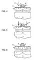
- FIG. 4shows the structure of FIG. 3 undergoing source/drain implantation
- FIG. 5shows the structure of FIG. 4 undergoing an inversion implantation
- FIG. 6shows the structure of FIG. 5 after a rapid thermal anneal
- FIG. 7shows the structure of FIG. 6 undergoing a punch-through prevention implantation
- FIG. 8shows the structure of FIG. 7 undergoing a shallow channel implantation
- FIG. 9shows the structure of FIG. 8 undergoing a deep channel implantation
- FIG.10shows the structure of FIG. 9 undergoing source/drain extension junction implantation
- FIG. 11shows the fully depleted silicon on insulator device of the present invention.
- a silicon on insulator (SOI) wafer 10which includes a semiconductor substrate 12 of a material such as a p-doped silicon (Si). On top of the semiconductor substrate 12 is a buried insulator layer 14 of a material such as a silicon dioxide (SiO 2 ) layer, and a shallow trench isolation 16 , also of a material such as SiO 2 , containing a semiconductor island 18 of a material such as a thin Si layer.
- SOIsilicon on insulator
- FIG. 2therein is shown the structure of FIG. 1 after the conventional deposition, patterning, photolithography, and etching to form a gate dielectric 20 of a material such as silicon dioxide, silicon oxynitride (SiON) or nitride (SiN 2 ), and a floating gate 22 of a material such as polysilicon or amorphous silicon which can be either doped or undoped.
- a gate dielectric 20of a material such as silicon dioxide, silicon oxynitride (SiON) or nitride (SiN 2 )
- a floating gate 22of a material such as polysilicon or amorphous silicon which can be either doped or undoped.
- FIG. 3therein is shown the structure of FIG. 2 with a liner 24 of a material such as a silicon dioxide (SiO 2 ) deposited on the shallow trench isolation 16 , the gate dielectric 20 , and the floating gate 22 .
- a spacer 26 of a material such as a Si 3 N 4is formed around the gate portion of the liner 24 .
- the spacer 26is over-etched to the point that some of the liner 24 is etched away as shown by a step 28 .
- the width of the spacer 26determines the energy of subsequent implants because it controls the lateral diffusion of the implant underneath the spacer 26 . In the best mode the width is in the range of 400-1000 ⁇ and preferably around 500 ⁇ .
- a source/drain mask(not shown) is used to implant an n-type dopant, such as arsenic (As) to a depth of about one-third of the depth of the semiconductor island 18 .
- the implant energyis selected to be between 15 to 20 KeV so that the implant will reach a depth of between 300 to 500 ⁇ .
- the objectiveis to have the implant drive down sufficiently deep that a subsequent rapid thermal anneal (RTA) will eventually drive the implant down to at least 700 ⁇ .
- RTArapid thermal anneal
- the dopantdoes not need to go all the way down to the buried insulator level 14 because the depletion width of source/drain junctions 34 and 36 will be high enough that the source/drain contacts will be fully depleted on the buried insulator layer 14 . If the implant has a final depth of less than 700 ⁇ , it will not be possible to fully deplete the semiconductor island 18 and there will be increased junction capacitance, which is not desirable.
- a n-type dopant implantation 38which will invert the p-doped silicon in the semiconductor substrate 12 to form an n-silicon region 40 .
- the floating n-regionis implanted into the p-semiconductor substrate 12 to electrically prevent the electric fields from the drain to reach through the insulator to the source during operation because the electric field will cause a leakage path for the current to flow.
- the n-silicon region 40will prevent flow of current from the drain through the buried insulator layer 14 to the source.
- the implantation 38is a high-energy implant around 150 to 200 KeV with a dopant concentration in the range of 5e12 (5 ⁇ 10 12 ) to 1e13 cm 2 (1 ⁇ 10 13 )to fully deplete the channel 32 in subsequent steps. If a higher dose is used, the dopant will accumulate underneath the floating gate 22 near the interface between the semiconductor island 18 and the buried insulator layer 14 and will be very difficult to counter-dope later. A high counter-doping with a material such as boron (B) will again prevent full depletion of the channel 32 .
- a materialsuch as boron (B)
- FIG. 6therein is shown the result of an RTA performed on the SOI wafer 10 .
- the RTAwill cause enhanced thermal diffusion of the dopants to the desired locations.
- the RTAis from 5 to 10 seconds at temperatures in the range from 1025 to 1050° C. This will drive the dopants in the source/drain junctions 34 and 36 to the depth of two-thirds the semiconductor island 18 or 750-800 ⁇ .
- FIG. 7therein is shown the structure of FIG. 6 being subjected to a punch-through prevention implantation 44 using a dopant to form punch-through prevention regions 46 and 47 .
- the floating gate 22is used as a mask to implant the dopants at the edges of and underneath the source/drain junctions 34 and 36 , but not in the channel 32 because that would increase the total concentration of acceptors in the channel 32 and make it difficult to fully deplete the channel 32 afterward.
- the shallow channel implantation 48is preferably performed at a tilt of 45° from the vertical but may range from 25°-45° because of the necessity to integrate various other semiconductor devices on the wafer which may have shadowing effects due to the masking of one device on another.
- the shallow channel implantation 48is performed with a dopant such as boron difluoride (BF 2 ) and the energy is from 25 to 35 KeV.
- a dopantsuch as boron difluoride (BF 2 ) and the energy is from 25 to 35 KeV.
- a deep channel implant 54which is a deeper implant than the shallow channel implantation 48 and which forms the deep channel implant regions 55 and 56 .
- the deep channel implantation 52is performed around the floating gate 22 at various angles ranging from 25°-45° with 45 ° being preferred.
- the deep channel implant 52is preferably performed with a dopant such as B with the implantation energy in the range from 11 to 15 KeV.
- FIG. 10therein is shown a source/drain extension junction implantation 57 , which forms the source/drain extension junctions 58 and 60 .
- the source/drain extension junctions 58 and 60are formed with an n-type dopant, such as phosphorus (P), which is implanted at an energy level from 3 to 5 KeV, to take into account variations in the liner thickness, and at a low-dosage of from 3e14 to 8e14 cm 2 .
- Pphosphorus
- the annealcan be a very short RTA for 1 to 2 seconds at 1000° C., or can be a spike RTA of a temperature up to 1025° C. to fully deplete the semiconductor island 18 with source/drain extension junctions 58 and 60 and source/drain junctions 34 and 36 .
- a spacer 62has also been deposited which is used in forming the contact connection silicide. The spacer 62 causes the silicide to form as salicide (self-aligned silicide) regions 64 , 66 , and 68 , which are respectively formed over the source/drain junction 34 , the floating gate 22 , and the source/drain junction 36 .
- the silicon island 18can range from 200 to 2000 ⁇ thick with the thinner thicknesses making it easier to fully deplete the silicon island 18 .
- the thickness used for non-fully depleted SOIcurrently is 1000 ⁇ and the parameters of the preferred mode are optimized for this thickness silicon island.
- the buried insulator layer 14can range from 200 to 2000 ⁇ thick with the thinner thickness making it easier to fully deplete the silicon island 18 .
- capacitive coupling of the floating gate 22 and the silicon island 18will deteriorate the sub-threshold voltage slope, which is related to changes in the doping.
- the current standard for non-fully depleted devicesis around 2000 ⁇ thick for the buried insulator layer 14 and the parameters of the preferred mode are optimized for this thickness silicon island 18 .
Landscapes
- Thin Film Transistor (AREA)
Abstract
Description
Claims (15)
Priority Applications (2)
| Application Number | Priority Date | Filing Date | Title |
|---|---|---|---|
| US09/511,418US6339244B1 (en) | 2000-02-22 | 2000-02-22 | Fully depleted silicon on insulator semiconductor device and manufacturing method therefor |
| US09/974,217US6579750B1 (en) | 2000-02-22 | 2001-10-09 | Manufacturing method for fully depleted silicon on insulator semiconductor device |
Applications Claiming Priority (1)
| Application Number | Priority Date | Filing Date | Title |
|---|---|---|---|
| US09/511,418US6339244B1 (en) | 2000-02-22 | 2000-02-22 | Fully depleted silicon on insulator semiconductor device and manufacturing method therefor |
Related Child Applications (1)
| Application Number | Title | Priority Date | Filing Date |
|---|---|---|---|
| US09/974,217DivisionUS6579750B1 (en) | 2000-02-22 | 2001-10-09 | Manufacturing method for fully depleted silicon on insulator semiconductor device |
Publications (1)
| Publication Number | Publication Date |
|---|---|
| US6339244B1true US6339244B1 (en) | 2002-01-15 |
Family
ID=24034819
Family Applications (2)
| Application Number | Title | Priority Date | Filing Date |
|---|---|---|---|
| US09/511,418Expired - LifetimeUS6339244B1 (en) | 2000-02-22 | 2000-02-22 | Fully depleted silicon on insulator semiconductor device and manufacturing method therefor |
| US09/974,217Expired - LifetimeUS6579750B1 (en) | 2000-02-22 | 2001-10-09 | Manufacturing method for fully depleted silicon on insulator semiconductor device |
Family Applications After (1)
| Application Number | Title | Priority Date | Filing Date |
|---|---|---|---|
| US09/974,217Expired - LifetimeUS6579750B1 (en) | 2000-02-22 | 2001-10-09 | Manufacturing method for fully depleted silicon on insulator semiconductor device |
Country Status (1)
| Country | Link |
|---|---|
| US (2) | US6339244B1 (en) |
Cited By (19)
| Publication number | Priority date | Publication date | Assignee | Title |
|---|---|---|---|---|
| US6413829B1 (en)* | 2001-06-01 | 2002-07-02 | Advanced Micro Devices, Inc. | Field effect transistor in SOI technology with schottky-contact extensions |
| US6432777B1 (en)* | 2001-06-06 | 2002-08-13 | International Business Machines Corporation | Method for increasing the effective well doping in a MOSFET as the gate length decreases |
| US20030126525A1 (en)* | 2001-12-06 | 2003-07-03 | Koji Miyashita | Semiconductor device, method of testing the same and electronic instrument |
| US6605843B1 (en)* | 2000-08-11 | 2003-08-12 | Advanced Micro Devices, Inc. | Fully depleted SOI device with tungsten damascene contacts and method of forming same |
| US20030227058A1 (en)* | 2002-06-05 | 2003-12-11 | Hongmei Wang | Fully-depleted (FD) (SOI) MOSFET access transistor and method of fabrication |
| US20040004298A1 (en)* | 2002-07-08 | 2004-01-08 | Madurawe Raminda U. | Semiconductor latches and SRAM devices |
| US20040004251A1 (en)* | 2002-07-08 | 2004-01-08 | Madurawe Raminda U. | Insulated-gate field-effect thin film transistors |
| US20040004252A1 (en)* | 2002-07-08 | 2004-01-08 | Madurawe Raminda U. | Semiconductor switching devices |
| US20040152279A1 (en)* | 2002-07-08 | 2004-08-05 | Madurawe Raminda Udaya | Semiconductor latches and SRAM devices |
| US6787851B2 (en)* | 2000-12-19 | 2004-09-07 | Seiko Epson Corporation | Semiconductor devices including a silicon-on-insulator layer |
| US6787423B1 (en) | 2002-12-09 | 2004-09-07 | Advanced Micro Devices, Inc. | Strained-silicon semiconductor device |
| US20040214389A1 (en)* | 2002-07-08 | 2004-10-28 | Madurawe Raminda Udaya | Semiconductor latches and SRAM devices |
| US20060099752A1 (en)* | 2004-11-10 | 2006-05-11 | Advanced Micro Devices, Inc. | Strained fully depleted silicon on insulator semiconductor device and manufacturing method therefor |
| US20060145256A1 (en)* | 2003-06-11 | 2006-07-06 | Koninklijke Philips Electronics N.C. | Prevention of parasitic channel in an integrated soi process |
| CN100401528C (en)* | 2002-01-23 | 2008-07-09 | 斯平内克半导体股份有限公司 | Field effect transistor with source and/or drain forming schottky or schottky-like contact with strained semiconductor substrate |
| US20100019322A1 (en)* | 2008-07-23 | 2010-01-28 | International Business Machines Corporation | Semiconductor device and method of manufacturing |
| US20110254089A1 (en)* | 1994-05-26 | 2011-10-20 | Semiconductor Energy Laboratory Co., Ltd. | Semiconductor integrated circuit and method of fabricating same |
| US20150187957A1 (en)* | 2013-12-31 | 2015-07-02 | Texas Instruments Incorporated | Transistor with improved radiation hardness |
| US11810951B2 (en) | 2021-12-16 | 2023-11-07 | Globalfoundries U.S. Inc. | Semiconductor-on-insulator field effect transistor with performance-enhancing source/drain shapes and/or materials |
Families Citing this family (7)
| Publication number | Priority date | Publication date | Assignee | Title |
|---|---|---|---|---|
| US20030082892A1 (en)* | 2001-10-31 | 2003-05-01 | Macronix International Co., Ltd. | Method for reducing the drain coupling ratio of floating gate device |
| US6870225B2 (en)* | 2001-11-02 | 2005-03-22 | International Business Machines Corporation | Transistor structure with thick recessed source/drain structures and fabrication process of same |
| US7416927B2 (en)* | 2002-03-26 | 2008-08-26 | Infineon Technologies Ag | Method for producing an SOI field effect transistor |
| US6882829B2 (en)* | 2002-04-02 | 2005-04-19 | Texas Instruments Incorporated | Integrated circuit incorporating RF antenna switch and power amplifier |
| US6703281B1 (en)* | 2002-10-21 | 2004-03-09 | Advanced Micro Devices, Inc. | Differential laser thermal process with disposable spacers |
| US7939861B2 (en)* | 2007-02-02 | 2011-05-10 | Synopsys, Inc. | Non-volatile memory devices having floating-gates FETs with different source-gate and drain-gate border lengths |
| US10804394B2 (en)* | 2018-09-20 | 2020-10-13 | Avago Technologies International Sales Pte. Limited | Fin structures on a fully depleted semiconductor layer including a channel region |
Citations (5)
| Publication number | Priority date | Publication date | Assignee | Title |
|---|---|---|---|---|
| JPH05136418A (en)* | 1992-04-27 | 1993-06-01 | Seiko Epson Corp | Semiconductor device |
| US5359219A (en)* | 1992-12-04 | 1994-10-25 | Texas Instruments Incorporated | Silicon on insulator device comprising improved substrate doping |
| US6043535A (en)* | 1997-08-29 | 2000-03-28 | Texas Instruments Incorporated | Self-aligned implant under transistor gate |
| US6100567A (en)* | 1998-06-11 | 2000-08-08 | Sun Microsystems, Inc. | Tunable threshold SOI device using back gate and intrinsic channel region |
| US6180983B1 (en)* | 1998-07-17 | 2001-01-30 | National Semiconductor Corporation | High-voltage MOS transistor on a silicon on insulator wafer |
Family Cites Families (3)
| Publication number | Priority date | Publication date | Assignee | Title |
|---|---|---|---|---|
| US5208168A (en)* | 1990-11-26 | 1993-05-04 | Motorola, Inc. | Semiconductor device having punch-through protected buried contacts and method for making the same |
| US6342423B1 (en)* | 1999-09-24 | 2002-01-29 | Advanced Micro Devices, Inc. | MOS-type transistor processing utilizing UV-nitride removable spacer and HF etch |
| US6190982B1 (en)* | 2000-01-28 | 2001-02-20 | United Microelectronics Corp. | Method of fabricating a MOS transistor on a semiconductor wafer |
- 2000
- 2000-02-22USUS09/511,418patent/US6339244B1/ennot_activeExpired - Lifetime
- 2001
- 2001-10-09USUS09/974,217patent/US6579750B1/ennot_activeExpired - Lifetime
Patent Citations (5)
| Publication number | Priority date | Publication date | Assignee | Title |
|---|---|---|---|---|
| JPH05136418A (en)* | 1992-04-27 | 1993-06-01 | Seiko Epson Corp | Semiconductor device |
| US5359219A (en)* | 1992-12-04 | 1994-10-25 | Texas Instruments Incorporated | Silicon on insulator device comprising improved substrate doping |
| US6043535A (en)* | 1997-08-29 | 2000-03-28 | Texas Instruments Incorporated | Self-aligned implant under transistor gate |
| US6100567A (en)* | 1998-06-11 | 2000-08-08 | Sun Microsystems, Inc. | Tunable threshold SOI device using back gate and intrinsic channel region |
| US6180983B1 (en)* | 1998-07-17 | 2001-01-30 | National Semiconductor Corporation | High-voltage MOS transistor on a silicon on insulator wafer |
Non-Patent Citations (1)
| Title |
|---|
| T. Kachi, T. Kaga, S. Wakahara, and D. Hisamoto "Variable Threshold-Voltage SOI CMOSFETs with Implanted Back-Gate Electrodes for Power-Managed Low-Power and High-Speed sub-1-V ULSIs", 1996 Symposium on VSLI Technology Digest of Technical Papers, pp. 124-125. |
Cited By (42)
| Publication number | Priority date | Publication date | Assignee | Title |
|---|---|---|---|---|
| US20110254089A1 (en)* | 1994-05-26 | 2011-10-20 | Semiconductor Energy Laboratory Co., Ltd. | Semiconductor integrated circuit and method of fabricating same |
| US6605843B1 (en)* | 2000-08-11 | 2003-08-12 | Advanced Micro Devices, Inc. | Fully depleted SOI device with tungsten damascene contacts and method of forming same |
| US6787851B2 (en)* | 2000-12-19 | 2004-09-07 | Seiko Epson Corporation | Semiconductor devices including a silicon-on-insulator layer |
| US6413829B1 (en)* | 2001-06-01 | 2002-07-02 | Advanced Micro Devices, Inc. | Field effect transistor in SOI technology with schottky-contact extensions |
| US6432777B1 (en)* | 2001-06-06 | 2002-08-13 | International Business Machines Corporation | Method for increasing the effective well doping in a MOSFET as the gate length decreases |
| US20030126525A1 (en)* | 2001-12-06 | 2003-07-03 | Koji Miyashita | Semiconductor device, method of testing the same and electronic instrument |
| CN100401528C (en)* | 2002-01-23 | 2008-07-09 | 斯平内克半导体股份有限公司 | Field effect transistor with source and/or drain forming schottky or schottky-like contact with strained semiconductor substrate |
| US20030227058A1 (en)* | 2002-06-05 | 2003-12-11 | Hongmei Wang | Fully-depleted (FD) (SOI) MOSFET access transistor and method of fabrication |
| US8148225B2 (en) | 2002-06-05 | 2012-04-03 | Micron Technology, Inc. | Fully-depleted (FD)(SOI) MOSFET access transistor and method of fabrication |
| US7517743B2 (en) | 2002-06-05 | 2009-04-14 | Micron Technology, Inc. | Fully-depleted (FD) (SOI) MOSFET access transistor and method of fabrication |
| US20040135204A1 (en)* | 2002-06-05 | 2004-07-15 | Hongmei Wang | Fully-depleted (FD) (SOI) MOSFET access transistor and method of fabrication |
| US7465999B2 (en) | 2002-06-05 | 2008-12-16 | Micron Technology, Inc. | Fully-depleted (FD) (SOI) MOSFET access transistor |
| US7189606B2 (en) | 2002-06-05 | 2007-03-13 | Micron Technology, Inc. | Method of forming fully-depleted (FD) SOI MOSFET access transistor |
| US7151303B2 (en) | 2002-06-05 | 2006-12-19 | Micron Technology, Inc. | Fully-depleted (FD) (SOI) MOSFET access transistor |
| US20050121721A1 (en)* | 2002-07-08 | 2005-06-09 | Madurawe Raminda U. | Insulated-gate field-effect thin film transistors |
| US20040207100A1 (en)* | 2002-07-08 | 2004-10-21 | Raminda Udaya Madurawe | Semiconductor latches and sram devices |
| US20050007839A1 (en)* | 2002-07-08 | 2005-01-13 | Madurawe Raminda Udaya | Semiconductor switching devices |
| US6849958B2 (en) | 2002-07-08 | 2005-02-01 | Viciciv | Semiconductor latches and SRAM devices |
| US6856030B2 (en) | 2002-07-08 | 2005-02-15 | Viciciv Technology | Semiconductor latches and SRAM devices |
| US6855988B2 (en) | 2002-07-08 | 2005-02-15 | Viciciv Technology | Semiconductor switching devices |
| US20040214389A1 (en)* | 2002-07-08 | 2004-10-28 | Madurawe Raminda Udaya | Semiconductor latches and SRAM devices |
| US20050146942A1 (en)* | 2002-07-08 | 2005-07-07 | Madurawe Raminda U. | Semiconductor switching devices |
| US6998722B2 (en) | 2002-07-08 | 2006-02-14 | Viciciv Technology | Semiconductor latches and SRAM devices |
| US7018875B2 (en) | 2002-07-08 | 2006-03-28 | Viciciv Technology | Insulated-gate field-effect thin film transistors |
| US7030446B2 (en) | 2002-07-08 | 2006-04-18 | Viciciv Technology | Semiconductor switching devices |
| US20040004298A1 (en)* | 2002-07-08 | 2004-01-08 | Madurawe Raminda U. | Semiconductor latches and SRAM devices |
| US20040004251A1 (en)* | 2002-07-08 | 2004-01-08 | Madurawe Raminda U. | Insulated-gate field-effect thin film transistors |
| US6828689B2 (en) | 2002-07-08 | 2004-12-07 | Vi Ci Civ | Semiconductor latches and SRAM devices |
| US20040004252A1 (en)* | 2002-07-08 | 2004-01-08 | Madurawe Raminda U. | Semiconductor switching devices |
| US7265421B2 (en) | 2002-07-08 | 2007-09-04 | Viciciv Technology | Insulated-gate field-effect thin film transistors |
| US20040152279A1 (en)* | 2002-07-08 | 2004-08-05 | Madurawe Raminda Udaya | Semiconductor latches and SRAM devices |
| US20080067594A1 (en)* | 2002-07-08 | 2008-03-20 | Madurawe Raminda U | Insulated-gate field-effect thin film transistors |
| US20040152245A1 (en)* | 2002-07-08 | 2004-08-05 | Madurawe Raminda U. | Insulated-gate field-effect thin film transistors |
| US6787423B1 (en) | 2002-12-09 | 2004-09-07 | Advanced Micro Devices, Inc. | Strained-silicon semiconductor device |
| US7544998B2 (en)* | 2003-06-11 | 2009-06-09 | Nxp B.V. | Prevention of parasitic channel in an integrated SOI process |
| US20060145256A1 (en)* | 2003-06-11 | 2006-07-06 | Koninklijke Philips Electronics N.C. | Prevention of parasitic channel in an integrated soi process |
| US7306997B2 (en) | 2004-11-10 | 2007-12-11 | Advanced Micro Devices, Inc. | Strained fully depleted silicon on insulator semiconductor device and manufacturing method therefor |
| US20060099752A1 (en)* | 2004-11-10 | 2006-05-11 | Advanced Micro Devices, Inc. | Strained fully depleted silicon on insulator semiconductor device and manufacturing method therefor |
| US8502283B2 (en) | 2004-11-10 | 2013-08-06 | Globalfoundries Inc. | Strained fully depleted silicon on insulator semiconductor device |
| US20100019322A1 (en)* | 2008-07-23 | 2010-01-28 | International Business Machines Corporation | Semiconductor device and method of manufacturing |
| US20150187957A1 (en)* | 2013-12-31 | 2015-07-02 | Texas Instruments Incorporated | Transistor with improved radiation hardness |
| US11810951B2 (en) | 2021-12-16 | 2023-11-07 | Globalfoundries U.S. Inc. | Semiconductor-on-insulator field effect transistor with performance-enhancing source/drain shapes and/or materials |
Also Published As
| Publication number | Publication date |
|---|---|
| US6579750B1 (en) | 2003-06-17 |
Similar Documents
| Publication | Publication Date | Title |
|---|---|---|
| US6339244B1 (en) | Fully depleted silicon on insulator semiconductor device and manufacturing method therefor | |
| US6596554B2 (en) | Body-tied-to-source partially depleted SOI MOSFET | |
| US6420218B1 (en) | Ultra-thin-body SOI MOS transistors having recessed source and drain regions | |
| US6441436B1 (en) | SOI device and method of fabrication | |
| US6372559B1 (en) | Method for self-aligned vertical double-gate MOSFET | |
| US5444282A (en) | Semiconductor device and a method of manufacturing thereof | |
| KR100243715B1 (en) | CMOS structure with FET in isolated well with depletion unit and method | |
| US6204138B1 (en) | Method for fabricating a MOSFET device structure which facilitates mitigation of junction capacitance and floating body effects | |
| US6288425B1 (en) | SOI-MOSFET device | |
| US6177299B1 (en) | Transistor having substantially isolated body and method of making the same | |
| US6437404B1 (en) | Semiconductor-on-insulator transistor with recessed source and drain | |
| JPH11330454A (en) | Semiconductor device and manufacturing method thereof | |
| JP2701762B2 (en) | Semiconductor device and manufacturing method thereof | |
| JPH11274496A (en) | FIELD EFFECT TRANSISTOR HAVING IMPROVED IMPLANT AND METHOD OF MANUFACTURING THE SAME | |
| US6724049B2 (en) | SOI semiconductor device with insulating film having different properties relative to the buried insulating film | |
| US6198114B1 (en) | Field effect transistor having dielectrically isolated sources and drains and method for making same | |
| EP1024537A2 (en) | Insulated gate field effect transistor having a buried region and method of making the same | |
| CN100448026C (en) | Semiconductor structures and methods of forming them | |
| US6605843B1 (en) | Fully depleted SOI device with tungsten damascene contacts and method of forming same | |
| US6930357B2 (en) | Active SOI structure with a body contact through an insulator | |
| US20020063285A1 (en) | SOI device and method of fabrication | |
| CN101661889B (en) | Manufacturing method of silicon MOS transistor on partially consumed insulating layer | |
| US6525378B1 (en) | Raised S/D region for optimal silicidation to control floating body effects in SOI devices | |
| US6420767B1 (en) | Capacitively coupled DTMOS on SOI | |
| US6359298B1 (en) | Capacitively coupled DTMOS on SOI for multiple devices |
Legal Events
| Date | Code | Title | Description |
|---|---|---|---|
| AS | Assignment | Owner name:ADVANCED MICRO DEVICES, INC., CALIFORNIA Free format text:ASSIGNMENT OF ASSIGNORS INTEREST;ASSIGNOR:KRIVOKAPIC, ZORAN;REEL/FRAME:010627/0434 Effective date:20000217 | |
| FEPP | Fee payment procedure | Free format text:PAYOR NUMBER ASSIGNED (ORIGINAL EVENT CODE: ASPN); ENTITY STATUS OF PATENT OWNER: LARGE ENTITY | |
| STCF | Information on status: patent grant | Free format text:PATENTED CASE | |
| FPAY | Fee payment | Year of fee payment:4 | |
| FPAY | Fee payment | Year of fee payment:8 | |
| AS | Assignment | Owner name:GLOBALFOUNDRIES INC., CAYMAN ISLANDS Free format text:AFFIRMATION OF PATENT ASSIGNMENT;ASSIGNOR:ADVANCED MICRO DEVICES, INC.;REEL/FRAME:023119/0083 Effective date:20090630 | |
| FPAY | Fee payment | Year of fee payment:12 | |
| AS | Assignment | Owner name:WILMINGTON TRUST, NATIONAL ASSOCIATION, DELAWARE Free format text:SECURITY AGREEMENT;ASSIGNOR:GLOBALFOUNDRIES INC.;REEL/FRAME:049490/0001 Effective date:20181127 | |
| AS | Assignment | Owner name:GLOBALFOUNDRIES INC., CAYMAN ISLANDS Free format text:RELEASE BY SECURED PARTY;ASSIGNOR:WILMINGTON TRUST, NATIONAL ASSOCIATION;REEL/FRAME:054636/0001 Effective date:20201117 | |
| AS | Assignment | Owner name:GLOBALFOUNDRIES U.S. INC., NEW YORK Free format text:RELEASE BY SECURED PARTY;ASSIGNOR:WILMINGTON TRUST, NATIONAL ASSOCIATION;REEL/FRAME:056987/0001 Effective date:20201117 |