US6339232B1 - Semiconductor device - Google Patents
Semiconductor deviceDownload PDFInfo
- Publication number
- US6339232B1 US6339232B1US09/665,682US66568200AUS6339232B1US 6339232 B1US6339232 B1US 6339232B1US 66568200 AUS66568200 AUS 66568200AUS 6339232 B1US6339232 B1US 6339232B1
- Authority
- US
- United States
- Prior art keywords
- field effect
- effect transistor
- channel
- layer
- channel field
- Prior art date
- Legal status (The legal status is an assumption and is not a legal conclusion. Google has not performed a legal analysis and makes no representation as to the accuracy of the status listed.)
- Expired - Lifetime
Links
Images


Classifications
- H—ELECTRICITY
- H10—SEMICONDUCTOR DEVICES; ELECTRIC SOLID-STATE DEVICES NOT OTHERWISE PROVIDED FOR
- H10D—INORGANIC ELECTRIC SEMICONDUCTOR DEVICES
- H10D86/00—Integrated devices formed in or on insulating or conducting substrates, e.g. formed in silicon-on-insulator [SOI] substrates or on stainless steel or glass substrates
- H10D86/201—Integrated devices formed in or on insulating or conducting substrates, e.g. formed in silicon-on-insulator [SOI] substrates or on stainless steel or glass substrates the substrates comprising an insulating layer on a semiconductor body, e.g. SOI
- H—ELECTRICITY
- H10—SEMICONDUCTOR DEVICES; ELECTRIC SOLID-STATE DEVICES NOT OTHERWISE PROVIDED FOR
- H10D—INORGANIC ELECTRIC SEMICONDUCTOR DEVICES
- H10D86/00—Integrated devices formed in or on insulating or conducting substrates, e.g. formed in silicon-on-insulator [SOI] substrates or on stainless steel or glass substrates
- H10D86/01—Manufacture or treatment
Definitions
- the present inventionrelates to a semiconductor device, and particularly to a semiconductor device including a complementary Metal-Oxide-Semiconductor field effect transistor (CMOSFET).
- CMOSFETcomplementary Metal-Oxide-Semiconductor field effect transistor
- MOSFETmetal/oxide/semiconductor field effect transistor
- a threshold voltagebecomes as high as 0.5 V or higher. Since a power voltage of 1 V or less is expected in the CMOSFET of the sub-0.1 micron generation, such a high threshold voltage causes a drop in current driving power of the MOSFET, and further, a drop in operation speed of a circuit.
- the present inventionhas been made in view of the above problem, and has an object to provide a semiconductor device in which gate electrodes of both an n-channel MOSFET and a p-channel MOSFET constituting a CHOSFET are made of the same material, and a threshold voltage of each of them is sufficiently decreased.
- Another object of the present inventionis to provide a semiconductor device that includes an n-channel MOSFET and a p-channel MOSFET constituting a CMOSFET and can be manufactured by a simplified process.
- a semiconductor devicecomprises a semiconductor substrate, and an n-channel field effect transistor and a p-channel field effect transistor respectively formed on the semiconductor substrate, the n-channel field effect transistor and the p-channel field effect transistor constitute a complementary field effect transistor, and the semiconductor device is characterized in that
- a gate electrode of the n-channel field effect transistor and a gate electrode of the p-channel field effect transistorare made of the same material
- a channel region of the n-channel field effect transistoris made of at least of Si and in which an energy difference between a conduction band edge and a vacuum level is higher than that of bulk Si
- a channel region of the p-channel field effect transistoris made of at least of Si and in which an energy difference between a valence band edge and the vacuum level is lower than that of bulk Si
- a work function of the material making the gate electrodesis higher than the energy difference between the conduction band edge of the material making the channel region of the n-channel field effect transistor and the vacuum level, and is lower than the energy difference between the valence band edge of the material making the channel region of the p-channel field effect transistor and the vacuum level.
- the material making the channel region of the n-channel field effect transistoris Si into which tensile stress is introduced. It is so-called strained Si in this specification.
- the material making the channel region of the p-channel field effect transistoris SiGe.
- the Fermi level EF of the gate electrode materialis ( 4 E v2 +E c1 )/5 or less and (E v2 + 4 E c1 )/5 or less, E v2 is the valence band edge of the material making the channel region of the p-channel field effect transistor and E v1 is the conduction band edge of the material making of the channel region of the n-channel field effect transistor.
- the Fermi level E F of the gate electrode materialis substantially (E v2 +E c1 )/2, E v2 is the valence band edge of the material making the channel region of the p-channel field effect transistor and E c1 is the conduction band edge of the material making of the channel region of the n-channel field effect transistor.
- E c1 of the channel material of the n-channel MOSFETis higher than (E v0 +E c0 )/ 10 and not higher than (E v0 +E c0 )/2, E v0 is the valence band edge of the bulk Si and E c0 is the conduction band edge of the bulk Si.
- E v2 of the channel material of the p-channel MOSFETis not less than (E v0 +E c0 )/2 and less than ( 9 E v0 +E c0 )/10, Evo is the valence band edge of the bulk Si and E c0 is the conduction band edge of the bulk Si.
- a semiconductor devicecomprises a semiconductor substrate
- n-channel field effect transistorformed on the semiconductor substrate; and a p-channel field effect transistor formed on the semiconductor substrate, the n-channel field effect transistor and the p-channel field effect transistor constituting a complementary field effect transistor, wherein a gate electrode of the n-channel field effect transistor and a gate electrode of the p-channel field effect transistor are made of a same material, wherein at least a part of a channel region of the n-channel field effect transistor is formed in a strained Si layer, wherein at least a part of a channel region of the p-channel field effect transistor is formed in a first SiGe layer, and wherein a work function of the material making the gate electrodes is higher than an energy difference between a conduction band edge of the strained Si layered and a vacuum level, and is lower than an energy difference between a valence band edge of the first SiGe layer and the vacuum level.
- the n-channel field effect transistorincludes a second SiGe layer, which has the same composition ratio as the first SiGe layer and is disposed between the semiconductor substrate and the strained Si layer, and a tensile stress is introduced into the strained Si layer from the second SiGe layer.
- the n-channel field effect transistorincludes a second SiGe layer which has a Ge concentration higher than the first SiGe layer and is disposed between the semiconductor substrate and the strained Si layer
- the p-channel field effect transistorincludes a third SiGe layer which has the same composition ratio as the second SiGe layer and is disposed between the semiconductor substrate and the first SiGe layer
- a tensile stressis introduced into the strained Si layer from the second SiGe layer
- compressive stressis introduced into the first SiGe layer from the third SiGe layer.
- the p-channel field effect transistorincludes a Si layer between the first SiGe layer the third SiGe layer.
- the first SiGe layercomposes Si 1 ⁇ x Ge x and the second SiGe layer composes Si 1 ⁇ y Ge y (y>x).
- the gate electrodes of the n-channel field effect transistor and p-channel field effect transistorare made of a material selected from the group consisting of metal, doped p-type polycrystalline Ge, and doped p-type polycrystalline SiGe.
- the semiconductor devicefurther comprises an insulating film between the semiconductor substrate and the n-channel field effect transistor/the p-channel field effect transistor.
- the semiconductor devicefurther comprises an insulating film between the semiconductor substrate and the complementary field effect transistor.
- a semiconductor devicecomprises a semiconductor substrate; an n-channel field effect transistor formed on the semiconductor substrate; and a p-channel field effect transistor formed on the semiconductor substrate, the n-channel field effect transistor and the p-channel field effect transistor constituting a complementary field effect transistor, wherein a gate electrode of the n-channel field effect transistor and a gate electrode of the p-channel field effect transistor are made of a same material, and wherein one of the n-channel field effect transistor and the p-channel field effect transistor includes a first semiconductor layer in which at least a part of a channel region is formed, the other of the n-channel field effect transistor and the p-channel field effect transistor includes a second semiconductor layer in which at least a part of a channel region is formed and a third semiconductor layer as its under layer, and the first semiconductor layer and the third semiconductor layer are made of a same material.
- the semiconductor devicecomprises further an insulating film between the semiconductor substrate and the complementary field effect transistor.
- a work function of the material making the gate electrodes of the n-channel field effect transistor and p-channel field effect transistoris higher than an energy difference between a conduction band edge of a material making the channel region of the n-channel field effect transistor and a vacuum level, and is lower than an energy difference between a valence band edge of a material making the channel region of the p-channel field effect transistor and the vacuum level.
- an energy difference between a conduction band edge of a material making the channel region of the n-channel field effect transistor and vacuum level and an energy difference between a valence band edge of a material making the channel region of the p-channel field effect transistor and the vacuum levelare controlled such as above described and a work function of the material making the gate electrodes is in an energy difference between two energies.
- the threshold of the n-channel field effect transistor and p-channel field effect transistorcan decrease.
- an energy difference between a conduction band edge of the strained Si and a vacuum levelcan be higher than that of bulk Si and vacuum level. Since at least apart of a channel region of the p-channel field effect transistor is formed in a SiGe, which is an energy difference between a valence band edge of Ge and vacuum level is lower than that of bulk Si and a vacuum level, an energy difference between a valence band edge of the SiGe and vacuum level can be lower than that of bulk Si and vacuum.
- An energy difference between a conduction band edge of the strained Si making the channel region of the n-channel field effect transistor and vacuum level and an energy difference between a valence band edge of the SiGe making the p-channel field effect transistor and the vacuum levelare controlled such as above described and a work function of the material making the gate electrode is in an energy difference between two energies.
- the threshold of the n-channel field effect transistor and p-channel field effect transistorcan decrease.
- a composition of the first semiconductor layer and the third semiconductor layeris same and a tensile stress is introduced into the second semiconductor layer from the third semiconductor layer.
- the first and third semiconductor layersare deposited at same time.
- the tensile stressis introduced into the second semiconductor layer by depositing the second semiconductor layer on the third semiconductor layer.
- the second semiconductor layercan be strained with no increasing of another procedure, comparing to comprise the first and second semiconductor layer by different material.
- a method of manufacturing a semiconductor device including a semiconductor substrate, and an n-channel field effect transistor and a p-channel field effect transistor respectively formed on the semiconductor substrate, the n-channel field effect transistor and the p-channel field effect transistor constituting a complementary field effect transistorthe method is characterized by comprises;
- first semiconductor layeron one main surface of the semiconductor substrate; forming a second semiconductor layer on a part of the first semiconductor layer, into which tensile stress or compressive stress is introduced from the first semiconductor layer;
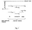
- FIG. 1is view showing schematically showing the principle of the present invention.
- FIGS. 2A to 2 Dare sectional views schematically showing a manufacturing method of a semiconductor device according to a first embodiment of the present invention, respectively.
- FIGS. 3A to 3 Care sectional views schematically showing a manufacturing method of a semiconductor device according to a second embodiment of the present invention, respectively.
- the basic structure of a semiconductor device of the present inventionincludes a CMOSFET constituted by an n-channel MOSFET and a p-channel MOSFET formed on a semiconductor substrate, a gate electrode of the n-channel MOSFET and a gate electrode of the p-channel MOSFET are made of the same material, and the material is selected such that the Fermi level of the gate electrode material is lower than the energy band of the conduction band edge of a semiconductor making a channel of the n-channel MOSFET, and is higher than the energy band of the valence band edge of a semiconductor making a channel of the p-channel MOSFET.
- the gate electrode materialis selected such that the work function thereof is higher than the energy difference between the conduction band edge of the semiconductor making the channel of the n-channel MOSFET and the vacuum level, and is lower than the energy difference between the valence band edge of the semiconductor making the channel of the p-channel MOSFET and the vacuum level.
- the inventionis characterized in that the semiconductor of the channel region of the n-channel MOSFET and the semiconductor of the channel region of the p-channel MOSPET are made of different materials.
- FIG. 2Dis a sectional view of a semiconductor device of an embodiment of the present invention.
- a semiconductor device 101 shown in FIG. 2Dincludes an n-channel MOSFET 3 and a p-channel MOSFET 41 on a semiconductor substrate 2 . These MOSFETs constitute a CMOSFET.
- the semiconductor substrate 2is, for example, a silicon substrate, and a SiGe layer 5 is formed on the surface of the substrate 2 and an oxide film 6 is formed on the SiGe layer 5 .
- the n-channel MOSFET 3has such a structure that a SiGe layer 7 , a Si layer 8 , a gate insulating film 9 , and a gate electrode 10 are sequentially laminated on the oxide film 6 . Both the SiGe layer 7 and the Si layer 8 are single crystals, and tensile stress is introduced into the Si layer 8 from the SiGe layer 7 . A channel region 11 is formed in the Si layer 8 . Besides, source/drain regions 12 doped with an n-type impurity at a high concentration are formed in the Si layer 8 at both sides of the channel region 11 .
- the p-channel MOSFET 41has such a structure that a SiGe layer 70 , a gate insulating film 90 , and a gate electrode 100 are sequentially laminated on the oxide film 6 .
- a channel region 13is formed in the SiGe layer 70 .
- source/drain regions 14 doped with a p-type impurity at a high concentrationare formed in the SiGe layer 70 at both sides of the channel region 13 .
- the gate electrode 10 of the n-channel MOSFET 3 and the gate electrode 100 of the p-channel MOSFET 41are formed of the same material, and its work function has the above described relation to the material making the channel region 11 of the n-channel MOSFET and the channel region 13 of the p-channel MOSFET.
- the channel region 11 of the n-channel MOSFETis made of strained silicon, and the energy difference between the conduction band edge of the strained silicon and the vacuum level is higher than the energy difference between the conduction band edge of bulk silicon and the vacuum level.
- the channel region 13 of the p-channel MOSFETis made of SiGe, and the energy difference between the valence band. edge of SiGe and the vacuum level is lower than the energy difference between the valence band edge of bulk silicon and the vacuum level.
- a threshold voltage V th of a MOSFETis simply given by the following expression (1).
- V thV FB +2 ⁇ B +2Q B /C ox (1)
- VFBis a flat band voltage
- ⁇ Bis a Fermi level in the substrate
- Q Bis a space charge surface density of the substrate
- C oxis a gate capacitance per unit area. If the gate oxide film is sufficiently thin in thickness, the term 3 of the above expression (1) can be ignored.
- threshold voltages V th nMOS and V th pMOS of the n-channel MOSPET and the p-channel MOSFETcan be expressed by the following expressions (2) and (3).
- Wis a work function of the gate electrode
- Ecis an energy difference between the conduction band edge of the semiconductor making the channel region of the n-channel MOSFET and the vacuum level
- Evis an energy difference between the valence band edge of the semiconductor making the channel region of the p-channel MOSFET and the vacuum level
- Egis a band gap of. the semiconductor making the channel region.
- the threshold voltagebecomes about 0.5 V which is almost half the band gap Eg of silicon. This value is too high in view of the fact that a power voltage of 1 V or less is expected in the sub-0.1 micron generation and the following.
- the channel regionIn order to decrease the threshold voltage, the channel region should be made of a semiconductor material having a band gap Eg lower than silicon. However, in that case, other problems such as a short channel effect and junction leak current. If a material deviated from the scope of silicon technology is used, a conventional manufacturing process can not be used and the industrial realization becomes low.
- the present inventionon the basis of consideration of the expressions (2) and (3), in the n-channel MOSFET, such a material is used that an energy difference Ec between the conduction band edge and the vacuum level is higher than that of bulk silicon, and in the p-channel MOSFET, such a material is used that an energy difference Ev between the valence band edge and the vacuum level is lower than that of bulk silicon.
- the gate electrodes of the n-channel MOSFET and the p-channel MOSFETthe same material is used, and the material satisfies such conditions that its work function is larger than Ec of the channel material of the n-channel MOSFET and is lower than Ev of the channel material of the p-channel MOSFET.
- FIG. 1is a view schematically showing the principle of the present invention, and is a band view showing a conduction band edge and a valence band edge of each of MOSFETs using silicon, strained silicon, and SiGe individually as a material making a channel region, and a Fermi level of a gate electrode.
- strained silicon having an conduction band E c1 and an valence band E v1is used as the channel material of the n-channel MOSFET.
- SiGe having conduction band E c2 and valence band E v2is used as the channel material of the p-channel MOSFET.
- a material having a Fermi level E F (work function W)is commonly used.
- FIG. 1shows silicon having conduction band edge E c0 and valence band edge E v0 for a channel.
- the Fermi level E F of the material making the gate electrodeis between the conduction band edge E c1 of strained Si that is the channel material of the n-channel MOSFET and the valence band edge E v2 of SiGe that is the channel material of the p-channel MOSFET.
- the work function W of the gate electrode materialis higher than the energy deference between conduction band edge E c1 of strained silicon and is lower than the energy deference between valence band edge E v2 of SiGe.
- the conduction band edge E c1 of strained Si that is the channel material of the n-channel MOSFETis lower than the conduction band edge E c0 of bulk Si.
- the valence band edge E v2 of SiGe that is the channel material of the p-channel MOSFETis higher than the valence band edge E v0 of bulk Si.
- the band gap between the conduction band edge of the n-channel MOSFET and the valence band edge of the p-channel MOSFETbecomes low, and the Fermi level of the gate electrode is between these, so the threshold voltage is decreased in both the n-channel and p-channel MOSFETs.
- the electron mobility of strained Siis increased by an effect that the strain exerts the band structure. Since the hole mobility of Ge is higher than that of Si, the hole mobility of the SiGe is higher than that of Si.
- the Fermi level E F of the gate electrode materialis ( 4 E v2 +E c1 )/5 or less and (E v2 + 4 E c1 )/5 or less. Further, it is more preferable that E F is substantially (E v2 +E c1 )/2. In this case, in both the n-channel MOSFET and the p-channel MOSFET, almost comparable threshold voltages can be realized.
- E c1 of the channel material of the n-channel MOSFETis higher than (E c0 + 9 E c0 )/ 10 and not higher than (E v0 +E c0 )/2.
- E v2 of the channel material of the p-channel MOSFETis not less than (E v0 +E c0 )/2 and less than ( 9 E v0 +E c0 )/10. In this case, it is possible to realize a threshold voltage that is sufficiently low and has no problem in practical use.
- the introduction of the tensile stress to the Si layercan be achieved by, for example, forming a thin film of the Si layer on an under layer made of SiGe by an epitaxial growth method. Since the lattice constant of SiGe is larger than Si, the strained Si layer can be obtained by epitaxial growth of thin Si layer on the SiGe layer.
- E c1 of the strained Si layercan be controlled by the magnitude of stress to be introduced. By controlling the lattice constant of the under layer of the Si layer, desired E c1 can be obtained.
- E v2 of the SiGe layercan be controlled by the composition ratio of Si and Ge.
- E v2 of the SiGe layercan also be controlled by introducing the stress to the SiGe layer. For example, when a single crystal Si layer is made an under layer and SiGe is formed on this layer by epitaxial growth, or when a single crystal SiGe layer is made an under layer and SiGe containing Ge at a concentration higher than that is formed on this layer by the epitaxial growth method, the SiGe layer to which compressive stress is introduced can be obtained. By doing so, it is possible to obtain the SiGe layer having higher E v2 .
- the Si layer formed on the SiGe under layer by the epitaxial growth methodmay be made the channel layer.
- the SiGe layermay be made the channel layer.
- FIGS. 2A to 2 Dare sectional views schematically showing a manufacturing method of CMOSPET of the first embodiment of the present invention.
- a semiconductor device 101 shown in FIG. 2Dincludes an. n-channel MOSFET 3 and a p-channel MOSFET 41 on a semiconductor substrate 2 .
- the semiconductor substrate 2is, for example, a silicon substrate, and a SiGe layer 5 and an oxide film 6 are formed on its surface region.
- the n-channel MOSFET 3has such a structure that a SiGe layer 7 , a Si layer 8 , a gate insulating film 9 , and a gate electrode 10 are sequentially laminated on the oxide film 6 . Both the SiGe layer 7 and the Si layer 8 are single crystals, and tensile stress is introduced into the Si layer 8 from the SiGe layer 7 . A channel region 11 is formed in the Si layer B. In the Si layer 8 , source/drain regions 12 doped with an n-type impurity at a high concentration are formed at both side of the channel region 11 .
- the p-channel MOSFET 41has such a structure that a SiGe layer 70 , a gate insulating film 90 , and a gate electrode 100 are sequentially laminated on the oxide film 6 .
- the channel region 13is formed in the SiGe layer 70 .
- source/drain regions 14 doped with a p-type impurity at a high concentrationare formed at both side of the channel region 13 .
- the n-channel MOSFET 3 and the p-channel MOSPET 41mutually constitute a CMOSFET.
- the semiconductor device 101 shown in FIG. 2Dcan be manufactured by, for example, a method described below.
- a SiGe buffer layer 15 and a Si 1 ⁇ x Ge x buffer layer 16are formed on one main surface of the silicon substrate 2 by an ultra high vacuum chemical vapor deposition (UHV-CVD) method.
- the SiGe buffer layer 15is a thin film having a concentration gradient in which a Ge concentration becomes high in a film thickness direction from the surface side of the silicon substrate 2 .
- the Si 1 ⁇ x Ge x buffer layer 16is a thin film having a constant Ge concentration, and normally, x is set within the range of 0.1 to 0.4.
- an oxygen ion of an injection dosage of 4 ⁇ 10 17 cm ⁇ 2is ion injected to the surface of the silicon substrate 2 on which the SiGe buffer layer 15 and the Si 1 ⁇ x Ge x buffer layer 16 are formed, and further, annealing is carried out at 1350° C. to 1200° C.
- the buried oxide film 6is formed in the Si 1 ⁇ x Ge x buffer layer 16 .
- the buried oxide film 6 formed in this wayis mainly made of silicon oxide and a region of about 400 nm from the surface of the Sil-xGeX buffer layer 16 remains not to be oxidized.
- the SiGe buffer layer 15 and the region of the Si 1 ⁇ x Ge x buffer layer 16 which remains not to be oxidizedare made the SiGe layers 5 and 7 , respectively.
- an oxide film 20such as a silicon oxide film is formed over the entire surface of the silicon substrate 2 on which the SiGe layer 7 is formed. Further, a part (region in which the n-channel MOSFET 3 is formed) of the oxide film 20 is removed, so a part of the SiGe layer 7 is exposed. Thereafter, Si is selectively epitaxially grown on the exposed SiGe layer 7 by the UHV-CVD method, so the Si layer 8 having a thickness of, for example, about 20 nm is formed. At this time, tensile strain is introduced into the Si layer 8 by the SiGe layer 7 of the lower layer. In the manner described above, the structure shown in FIG. 2B is obtained.
- the structure (except for the oxide film 20 ) shown in FIG. 2Bcan also be formed by using another method.
- Siis epitaxially grown on the whole surface of the SiGe layer 7 to form the Si layer 8 .
- an oxide filmis formed on the whole surface of the Si layer 8 , and its part is removed.
- an exposed portion of the Si layer 8is removed by etching.
- the structure (except for the oxide film 20 ) shown in FIG. 2Bcan be obtained also by such a method.
- the exposed portion of the Si layer 8is not completely removed by etching but may be made to remain by a thickness of about several nano meter.
- the part of the Si layer 8 made to remain like thiscan beaded the gate insulating film 9 in an oxidation step described later.
- the oxide film 20is removed.
- portions other than element regions, the SiGe layer 7 and the strained Si layer 8 on element separation regionsare removed by reactive ion etching (RIE), so the element regions are defined.
- RIEreactive ion etching
- the region corresponding to the n-channel MOSFET 3is denoted by the SiGe layer 7 and the strained Si layer 8
- the region corresponding to the p-channel MOSFET 41is denoted by the SiGe layer 70 .
- an impurity to suppress a short channel effectis ion injected to the region (part of the strained Si layer 8 and the SiGe layer 7 ) corresponding to the channel region 11 of the n-channel MOSFET 3 and the region (part of the SiGe layer 70 ) corresponding to the channel region 13 of the p-channel MOSFET 41 .
- the gate insulating film 9having a thickness of, for example, about 3 nm is formed by depositing an insulator or oxidizing the exposed surface.
- a metal layeris formed by depositing metal such as TiN or W through a sputtering method or the like over the whole surface of the substrate 2 on which the gate insulating film 9 is formed. Further, a resist pattern is formed on the metal layer, and RIE is carried out, so the gate electrode 10 of then-channel MOSFET 3 and the gate electrode 100 of the p-channel MOSFET are formed.
- the threshold of the n-channel MOSFETbecomes lower by 5.7 meV per 1%( Ge content) of SiGe under layer 7 .
- the threshold of the p-channel MOSFETbecomes lower by 7.7 meV per 1%( Ge content) of SiGe channel layer 13 .
- FIGS. 3A to 3 Care sectional views schematically showing a method of manufacturing a semiconductor device according to a second embodiment of the present invention.
- a semiconductor device 102 shown in FIG. 3Cincludes an n-channel MOSFET 3 and a p-channel MOSFET 42 on a semiconductor substrate 2 .
- the n-channel MOSFET 3 and the p-channel MOSFETconstitute a CMOSFET.
- the semiconductor device 102 shown in FIG. 3Cis different from the semiconductor device 101 shown in FIG. 2D in the structure of the p-channel MOSFET.
- the p-channel MOSPET 42has such a structure that a SiGe layer 70 , a Si layer 80 , a SiGe layer 21 , a gate insulating film 9 , and a gate electrode 100 are sequentially laminated on an oxide film 6 .
- the SiGe layer 70 , the Si layer 80 , and the SiGe layer 21are single crystals, and tensile stress is introduced into the Si layer 80 from the SiGe layer 70 .
- the SiGe layer 70is different from the SiGe layer 21 in the Ge concentration.
- the SiGe layer 70is made of Si 1 ⁇ x Ge x and the SiGe layer 21 is made of Si 1 ⁇ y Ge y
- the relation of y>xis established.
- the Ge concentrationis controlled so as to satisfy such a relation, compressive stress can be introduced from the Si layer 80 into the SiGe layer 21 .
- the energy level of the valence band edgecan be raised and the threshold voltage can be lowered.
- the semiconductor device 102 shown in FIG. 3Ccan be manufactured by, for example, a method described below.
- the procedure explained with reference to FIG. 2Ais carried out.
- an oxygen ion of an injection dosage of 4 ⁇ 10 17 cm ⁇ 2is ion injected to the surface of the silicon substrate 2 on which the SiGe buffer layer 15 and the Si 1 ⁇ x Ge x buffer layer 16 are formed, and further, annealing is carried out at 1350° C. to 1200° C.
- a buried oxide film 6is formed in the Si 1 ⁇ x Ge x buffer layer 16 .
- the region of about 400 nm from the surface of the Si 1 ⁇ x Ge x buffer layer 16remains not to be oxidized.
- the SiGe buffer layer 15 and the region of the Si 1 ⁇ x Ge x buffer layer 16 which remains not to be oxidizedare made the SiGe layers 5 and 7 , respectively.
- Siis epitaxially grown by the UHV-CVD method over the whole surface of the silicon substrate 2 on which the SiGe layer 7 is formed, so a Si layer 8 with a thickness of, for example, about 20 nm is formed. At this time, tensile strain is introduced into the Si layer 8 from the SiGe layer 7 of the under layer.
- an oxide film 20such as a silicon oxide film is formed over the whole surface of the silicon substrate 2 on which the Si layer 8 is formed. Further, a part (region where the p-channel MOSFET 42 is formed) of this oxide film 20 is removed to expose a part of the strained Si layer 8 . Thereafter, SiGe is selectively epitaxially grown on the strained Si layer 8 exposed by the UHV-CVD method, so a SiGe layer 21 with a thickness of, for example, about 20 nm is formed.
- the SiGe layer 21 made of Si 1 ⁇ x Ge xis formed so that the Ge concentration becomes high (y>x) as compared with the SiGe layer 7 made of Si 1 ⁇ y Ge y . In general, y is within the range of 0.2 to 1.0. By doing so, compressive strain is introduced into the SiGe layer 21 from the SiGe layer 7 . In the manner described above, the structure shown in FIG. 3A is obtained.
- the oxide film 20is removed.
- portions other than element regions, the SiGe layer 7 , the strained Si layer 8 , and the compressed SiGe layer 21 in element separation regionsare removed by reactive ion etching (RIE), so the element regions are defined.
- RIEreactive ion etching
- the region corresponding to the n-channel MOSFET 3is denoted by the SiGe layer 7 and the strained Si layer 8 .
- the region corresponding to the p-channel MOSFET 42is denoted by the SiGe layer 70 , the strained Si layer 80 , and the compressed SiGe layer 21 .
- an impurity to suppress a short channel effectis ion injected to the region (part of the strained Si layer 8 and the SiGe layer 7 ) corresponding to the channel region 11 of the n-channel MOSFET 3 and the region (part of the strained Si layer 80 , the SiGe layer 70 , and the SiGe layer 21 ) corresponding to the channel region 13 of the p-channel MOSFET 41 .
- a gate insulating film 9is formed by depositing an insulator or oxidizing the exposed surface.
- a metal layeris formed by depositing metal such as TiN or W through a sputtering method or the like over the whole surface of the substrate 2 on which the gate insulating film 9 is formed. Further, a resist pattern is formed on the metal layer and RIE is carried out, so a gate electrode 10 of the n-channel MOSFET 3 and a gate electrode 100 of the p-channel MOSFET 42 are formed.
- the gate electrode 10 of the n-channel MOSFET 3 and the gate electrode 100 of the p-channel MOSFET 41 or 42are made of TiN, W or the like, as long as a metal material is such that its work function is higher than the energy difference between the vacuum level and the conduction band edge of the strained Si layer 8 , and is lower than the energy difference between the vacuum level and the valence band edge of the SiGe layer 70 or the compressed SiGe layer 21 , the other metal material can also be used.
- the material making the gate electrode 10 of the n-channel MOSFET 3 and the gate electrode 100 of the p-channel MOSFET 41 or 42is not limited to the metal material, but poly Ge doped with a p-type impurity at a high concentration, Si 1 ⁇ y Ge y (y>x) or the like can also be used.
- the SOI MOSFET in which element separation and well separation is easyis adopted, a normal bulk MOSFET may be naturally adopted.
- the same materialcan be used for a gate electrode of an n-channel field effect transistor and a gate electrode of a p-channel field effect transistor.
- threshold voltages of both the n-channel field effect transistor and the p-channel field effect transistorcan be sufficiently lowered.
- a semiconductor devicewhich includes an n-channel field effect transistor and a p-channel field effect transistor constituting a complementary field effect transistor and can be manufactured by a simplified process.
Landscapes
- Metal-Oxide And Bipolar Metal-Oxide Semiconductor Integrated Circuits (AREA)
- Insulated Gate Type Field-Effect Transistor (AREA)
Abstract
Description
The present invention relates to a semiconductor device, and particularly to a semiconductor device including a complementary Metal-Oxide-Semiconductor field effect transistor (CMOSFET).
In recent years, the size of a CMOSFET has been miniaturized, and it is expected that the advancement is further made beyond the 0.1 μm generation. After this, it is considered that as the size is miniaturized more, various problems as indicated in the SIA (Semiconductor Industry Association) Roadmap occur.
As the size of the CMOSFET is miniaturized more, problems occur, one of which relates to a gate electrode. Conventionally, although polycrystalline silicon is used for the gate electrode, it is difficult to dope polycrystalline silicon with an impurity at a high concentration. Thus, there is a problem that a gate capacitance is lowered by depletion in polycrystalline silicon makes current driving power increase and interferes with suppression of a short channel effect.
In order to solve this problem, a CMOSFET using metal/oxide/semiconductor field effect transistor (MOSFET), in which metal is used as a material of a gate electrode, has been studied. However, in order to realize a CMOSFET of the sub-0.1 micron generation by using a metal gate, the following problem still remains.
In general, in a CMOSFET having a gate electrode made of metal, in order to simplify a manufacturing process, the same metal is used for the gate electrodes of an n-channel MOSFET and a p-channel MOSFET. In such a CMOSFET, in the case where an impurity concentration in a substrate is set so that the short channel effect is sufficiently suppressed, normally, in both of them, a threshold voltage becomes as high as 0.5 V or higher. Since a power voltage of 1 V or less is expected in the CMOSFET of the sub-0.1 micron generation, such a high threshold voltage causes a drop in current driving power of the MOSFET, and further, a drop in operation speed of a circuit.
The present invention has been made in view of the above problem, and has an object to provide a semiconductor device in which gate electrodes of both an n-channel MOSFET and a p-channel MOSFET constituting a CHOSFET are made of the same material, and a threshold voltage of each of them is sufficiently decreased.
Another object of the present invention is to provide a semiconductor device that includes an n-channel MOSFET and a p-channel MOSFET constituting a CMOSFET and can be manufactured by a simplified process.
According to a first aspect of the present invention, a semiconductor device comprises a semiconductor substrate, and an n-channel field effect transistor and a p-channel field effect transistor respectively formed on the semiconductor substrate, the n-channel field effect transistor and the p-channel field effect transistor constitute a complementary field effect transistor, and the semiconductor device is characterized in that
a gate electrode of the n-channel field effect transistor and a gate electrode of the p-channel field effect transistor are made of the same material,
a channel region of the n-channel field effect transistor is made of at least of Si and in which an energy difference between a conduction band edge and a vacuum level is higher than that of bulk Si, and a channel region of the p-channel field effect transistor is made of at least of Si and in which an energy difference between a valence band edge and the vacuum level is lower than that of bulk Si,
a work function of the material making the gate electrodes is higher than the energy difference between the conduction band edge of the material making the channel region of the n-channel field effect transistor and the vacuum level, and is lower than the energy difference between the valence band edge of the material making the channel region of the p-channel field effect transistor and the vacuum level.
At this time, it is preferable to introduce tensile stress into the material making the channel region of the n-channel field effect transistor.
It is preferable to introduce compressive stress into the material making the channel region of the p-channel field effect transistor.
It is preferable that the material making the channel region of the n-channel field effect transistor is Si into which tensile stress is introduced. It is so-called strained Si in this specification.
It is preferable that the material making the channel region of the p-channel field effect transistor is SiGe.
It is preferable that the Fermi level EF of the gate electrode material is (4Ev2+Ec1)/5 or less and (Ev2+4Ec1)/5 or less, Ev2is the valence band edge of the material making the channel region of the p-channel field effect transistor and Ev1is the conduction band edge of the material making of the channel region of the n-channel field effect transistor.
It is preferable that the Fermi level EFof the gate electrode material is substantially (Ev2+Ec1)/2, Ev2is the valence band edge of the material making the channel region of the p-channel field effect transistor and Ec1is the conduction band edge of the material making of the channel region of the n-channel field effect transistor.
It is preferable that Ec1of the channel material of the n-channel MOSFET is higher than (Ev0+Ec0)/ 10 and not higher than (Ev0+Ec0)/2, Ev0is the valence band edge of the bulk Si and Ec0is the conduction band edge of the bulk Si.
It is preferable that Ev2of the channel material of the p-channel MOSFET is not less than (Ev0+Ec0)/2 and less than (9Ev0+Ec0)/10, Evo is the valence band edge of the bulk Si and Ec0is the conduction band edge of the bulk Si.
According to a second aspect of the present invention, a semiconductor device comprises a semiconductor substrate;
an n-channel field effect transistor formed on the semiconductor substrate; and a p-channel field effect transistor formed on the semiconductor substrate, the n-channel field effect transistor and the p-channel field effect transistor constituting a complementary field effect transistor, wherein a gate electrode of the n-channel field effect transistor and a gate electrode of the p-channel field effect transistor are made of a same material, wherein at least a part of a channel region of the n-channel field effect transistor is formed in a strained Si layer, wherein at least a part of a channel region of the p-channel field effect transistor is formed in a first SiGe layer, and wherein a work function of the material making the gate electrodes is higher than an energy difference between a conduction band edge of the strained Si layered and a vacuum level, and is lower than an energy difference between a valence band edge of the first SiGe layer and the vacuum level.
It is preferable that the n-channel field effect transistor includes a second SiGe layer, which has the same composition ratio as the first SiGe layer and is disposed between the semiconductor substrate and the strained Si layer, and a tensile stress is introduced into the strained Si layer from the second SiGe layer.
It is preferable that the n-channel field effect transistor includes a second SiGe layer which has a Ge concentration higher than the first SiGe layer and is disposed between the semiconductor substrate and the strained Si layer, the p-channel field effect transistor includes a third SiGe layer which has the same composition ratio as the second SiGe layer and is disposed between the semiconductor substrate and the first SiGe layer, a tensile stress is introduced into the strained Si layer from the second SiGe layer, and compressive stress is introduced into the first SiGe layer from the third SiGe layer.
It is preferable that the p-channel field effect transistor includes a Si layer between the first SiGe layer the third SiGe layer.
It is preferable that the first SiGe layer composes Si1−xGexand the second SiGe layer composes Si1−yGey(y>x).
According to the first or second aspect of the invention, it is preferable that the gate electrodes of the n-channel field effect transistor and p-channel field effect transistor are made of a material selected from the group consisting of metal, doped p-type polycrystalline Ge, and doped p-type polycrystalline SiGe.
According to the first or second aspect of the invention, it is preferable that the semiconductor device further comprises an insulating film between the semiconductor substrate and the n-channel field effect transistor/the p-channel field effect transistor.
According to the first or second aspect of the invention, it is preferable that the semiconductor device further comprises an insulating film between the semiconductor substrate and the complementary field effect transistor.
According to the third aspect of the invention, a semiconductor device comprises a semiconductor substrate; an n-channel field effect transistor formed on the semiconductor substrate; and a p-channel field effect transistor formed on the semiconductor substrate, the n-channel field effect transistor and the p-channel field effect transistor constituting a complementary field effect transistor, wherein a gate electrode of the n-channel field effect transistor and a gate electrode of the p-channel field effect transistor are made of a same material, and wherein one of the n-channel field effect transistor and the p-channel field effect transistor includes a first semiconductor layer in which at least a part of a channel region is formed, the other of the n-channel field effect transistor and the p-channel field effect transistor includes a second semiconductor layer in which at least a part of a channel region is formed and a third semiconductor layer as its under layer, and the first semiconductor layer and the third semiconductor layer are made of a same material.
It is preferable that the semiconductor device comprises further an insulating film between the semiconductor substrate and the complementary field effect transistor.
It is preferable that a work function of the material making the gate electrodes of the n-channel field effect transistor and p-channel field effect transistor is higher than an energy difference between a conduction band edge of a material making the channel region of the n-channel field effect transistor and a vacuum level, and is lower than an energy difference between a valence band edge of a material making the channel region of the p-channel field effect transistor and the vacuum level.
According to the first aspect of the invention, an energy difference between a conduction band edge of a material making the channel region of the n-channel field effect transistor and vacuum level and an energy difference between a valence band edge of a material making the channel region of the p-channel field effect transistor and the vacuum level are controlled such as above described and a work function of the material making the gate electrodes is in an energy difference between two energies. Thus, the threshold of the n-channel field effect transistor and p-channel field effect transistor can decrease.
According to the second aspect of the invention, since at least a part of a channel region of the n-channel field effect transistor is formed in a strained Si layer, an energy difference between a conduction band edge of the strained Si and a vacuum level can be higher than that of bulk Si and vacuum level. Since at least apart of a channel region of the p-channel field effect transistor is formed in a SiGe, which is an energy difference between a valence band edge of Ge and vacuum level is lower than that of bulk Si and a vacuum level, an energy difference between a valence band edge of the SiGe and vacuum level can be lower than that of bulk Si and vacuum.
An energy difference between a conduction band edge of the strained Si making the channel region of the n-channel field effect transistor and vacuum level and an energy difference between a valence band edge of the SiGe making the p-channel field effect transistor and the vacuum level are controlled such as above described and a work function of the material making the gate electrode is in an energy difference between two energies. Thus, the threshold of the n-channel field effect transistor and p-channel field effect transistor can decrease.
According to the third aspect of the invention, a composition of the first semiconductor layer and the third semiconductor layer is same and a tensile stress is introduced into the second semiconductor layer from the third semiconductor layer. The first and third semiconductor layers are deposited at same time. The tensile stress is introduced into the second semiconductor layer by depositing the second semiconductor layer on the third semiconductor layer. The second semiconductor layer can be strained with no increasing of another procedure, comparing to comprise the first and second semiconductor layer by different material.
In order to produce the semiconductor of the invention, a method of manufacturing a semiconductor device including a semiconductor substrate, and an n-channel field effect transistor and a p-channel field effect transistor respectively formed on the semiconductor substrate, the n-channel field effect transistor and the p-channel field effect transistor constituting a complementary field effect transistor, the method is characterized by comprises;
forming a first semiconductor layer on one main surface of the semiconductor substrate; forming a second semiconductor layer on a part of the first semiconductor layer, into which tensile stress or compressive stress is introduced from the first semiconductor layer;
splitting the first and second semiconductor layers into elements correspondingly to the n-channel field effect transistor and the p-channel field effect transistor;
forming a gate insulating film on the first and second semiconductor layers;
forming gate electrodes on the gate insulating film correspondingly to the n-channel field effect transistor and the p-channel field effect transistor at the same time; and
injecting an impurity into the first and second semiconductor layers using the gate electrodes as masks.
FIG. 1 is view showing schematically showing the principle of the present invention.
FIGS. 2A to2D are sectional views schematically showing a manufacturing method of a semiconductor device according to a first embodiment of the present invention, respectively.
FIGS. 3A to3C are sectional views schematically showing a manufacturing method of a semiconductor device according to a second embodiment of the present invention, respectively.
Hereinafter, preferred embodiments of the present invention are described in more detail with reference to the drawings. Incidentally, the same members in the respective drawings are designated by the same reference numerals, and duplicate explanation is omitted.
The basic structure of a semiconductor device of the present invention includes a CMOSFET constituted by an n-channel MOSFET and a p-channel MOSFET formed on a semiconductor substrate, a gate electrode of the n-channel MOSFET and a gate electrode of the p-channel MOSFET are made of the same material, and the material is selected such that the Fermi level of the gate electrode material is lower than the energy band of the conduction band edge of a semiconductor making a channel of the n-channel MOSFET, and is higher than the energy band of the valence band edge of a semiconductor making a channel of the p-channel MOSFET.
In other words, the gate electrode material is selected such that the work function thereof is higher than the energy difference between the conduction band edge of the semiconductor making the channel of the n-channel MOSFET and the vacuum level, and is lower than the energy difference between the valence band edge of the semiconductor making the channel of the p-channel MOSFET and the vacuum level. As a result, a low threshold voltage is realized in both the n-channel MOSFET and the p-channel MOSFET, and the high speed operation of the CMOSFET is attained.
Further, at this time, the invention is characterized in that the semiconductor of the channel region of the n-channel MOSFET and the semiconductor of the channel region of the p-channel MOSPET are made of different materials.
FIG. 2D is a sectional view of a semiconductor device of an embodiment of the present invention.
Asemiconductor device 101 shown in FIG. 2D includes an n-channel MOSFET 3 and a p-channel MOSFET 41 on asemiconductor substrate 2. These MOSFETs constitute a CMOSFET. Thesemiconductor substrate 2 is, for example, a silicon substrate, and aSiGe layer 5 is formed on the surface of thesubstrate 2 and anoxide film 6 is formed on theSiGe layer 5.
The n-channel MOSFET 3 has such a structure that a SiGe layer7, aSi layer 8, agate insulating film 9, and agate electrode 10 are sequentially laminated on theoxide film 6. Both the SiGe layer7 and theSi layer 8 are single crystals, and tensile stress is introduced into theSi layer 8 from the SiGe layer7. Achannel region 11 is formed in theSi layer 8. Besides, source/drain regions 12 doped with an n-type impurity at a high concentration are formed in theSi layer 8 at both sides of thechannel region 11.
The p-channel MOSFET 41 has such a structure that aSiGe layer 70, a gate insulating film90, and agate electrode 100 are sequentially laminated on theoxide film 6. In the p-channel MOSFET 41, differently from the n-channel MOSFET 3, achannel region 13 is formed in theSiGe layer 70. Besides, source/drain regions 14 doped with a p-type impurity at a high concentration are formed in theSiGe layer 70 at both sides of thechannel region 13.
Thegate electrode 10 of the n-channel MOSFET 3 and thegate electrode 100 of the p-channel MOSFET 41 are formed of the same material, and its work function has the above described relation to the material making thechannel region 11 of the n-channel MOSFET and thechannel region 13 of the p-channel MOSFET.
Thechannel region 11 of the n-channel MOSFET is made of strained silicon, and the energy difference between the conduction band edge of the strained silicon and the vacuum level is higher than the energy difference between the conduction band edge of bulk silicon and the vacuum level.
Thechannel region 13 of the p-channel MOSFET is made of SiGe, and the energy difference between the valence band. edge of SiGe and the vacuum level is lower than the energy difference between the valence band edge of bulk silicon and the vacuum level.
Next, the principle of the present invention is described.
In general, a threshold voltage Vthof a MOSFET is simply given by the following expression (1).
Vth=VFB+2φB+2QB/Cox (1)
In the above expression (1), VFB is a flat band voltage, φBis a Fermi level in the substrate, QBis a space charge surface density of the substrate, and Coxis a gate capacitance per unit area. If the gate oxide film is sufficiently thin in thickness, theterm 3 of the above expression (1) can be ignored.
Thus, in the case where the gate electrodes and the channel regions of the n-channel MOSFET and the p-channel MOSFET are respectively made of the same materials, threshold voltages VthnMOSand VthpMOSof the n-channel MOSPET and the p-channel MOSFET can be expressed by the following expressions (2) and (3).
Incidentally, in the expressions (2) and (3), W is a work function of the gate electrode, Ec is an energy difference between the conduction band edge of the semiconductor making the channel region of the n-channel MOSFET and the vacuum level, Ev is an energy difference between the valence band edge of the semiconductor making the channel region of the p-channel MOSFET and the vacuum level, and Eg is a band gap of. the semiconductor making the channel region. Here, when usage of a CMOSFET is considered and the absolute values of the threshold voltages VthnMOSand VthnMOSof the n-channel MOSFET and the p-channel MOSFET are made coincident with each other, the following expressions (4) and (5) are obtained from the above expressions (2) and (3).

Thus, in the case where both the channel regions of the n-channel MOSFET and the p-channel MOSFET of the CMOSFET are made of silicon as usual, the threshold voltage becomes about 0.5 V which is almost half the band gap Eg of silicon. This value is too high in view of the fact that a power voltage of 1 V or less is expected in the sub-0.1 micron generation and the following.
In order to decrease the threshold voltage, the channel region should be made of a semiconductor material having a band gap Eg lower than silicon. However, in that case, other problems such as a short channel effect and junction leak current. If a material deviated from the scope of silicon technology is used, a conventional manufacturing process can not be used and the industrial realization becomes low.
According to the present invention, on the basis of consideration of the expressions (2) and (3), in the n-channel MOSFET, such a material is used that an energy difference Ec between the conduction band edge and the vacuum level is higher than that of bulk silicon, and in the p-channel MOSFET, such a material is used that an energy difference Ev between the valence band edge and the vacuum level is lower than that of bulk silicon. As the gate electrodes of the n-channel MOSFET and the p-channel MOSFET, the same material is used, and the material satisfies such conditions that its work function is larger than Ec of the channel material of the n-channel MOSFET and is lower than Ev of the channel material of the p-channel MOSFET. By constructing in this way, it is possible to effectively decrease the threshold voltage. This is described with reference to FIG.1.
FIG. 1 is a view schematically showing the principle of the present invention, and is a band view showing a conduction band edge and a valence band edge of each of MOSFETs using silicon, strained silicon, and SiGe individually as a material making a channel region, and a Fermi level of a gate electrode.
In the CMOSFET of the present invention, strained silicon having an conduction band Ec1and an valence band Ev1is used as the channel material of the n-channel MOSFET. SiGe having conduction band Ec2and valence band Ev2is used as the channel material of the p-channel MOSFET. For the respective gate electrodes, a material having a Fermi level EF(work function W) is commonly used. For comparison, FIG. 1 shows silicon having conduction band edge Ec0and valence band edge Ev0for a channel.
As shown in FIG. 1, the Fermi level EFof the material making the gate electrode is between the conduction band edge Ec1of strained Si that is the channel material of the n-channel MOSFET and the valence band edge Ev2of SiGe that is the channel material of the p-channel MOSFET. The work function W of the gate electrode material is higher than the energy deference between conduction band edge Ec1of strained silicon and is lower than the energy deference between valence band edge Ev2of SiGe.
As shown in FIG. 1, in the semiconductor device of the present invention, the conduction band edge Ec1of strained Si that is the channel material of the n-channel MOSFET is lower than the conduction band edge Ec0of bulk Si. The valence band edge Ev2of SiGe that is the channel material of the p-channel MOSFET is higher than the valence band edge Ev0of bulk Si. In the semiconductor device of the present invention, the band gap between the conduction band edge of the n-channel MOSFET and the valence band edge of the p-channel MOSFET becomes low, and the Fermi level of the gate electrode is between these, so the threshold voltage is decreased in both the n-channel and p-channel MOSFETs.
The electron mobility of strained Si is increased by an effect that the strain exerts the band structure. Since the hole mobility of Ge is higher than that of Si, the hole mobility of the SiGe is higher than that of Si. These facts mean that the CMOSFET of the present invention that the channel region of the n-channel MOSFET is made of strained Si and the channel region of the p-channel MOSFET is made of SiGe has high current drive power and is excellent in circuit performance. In the CMOSFET of the present invention, strained Si is used for the channel of the n-channel MOSFET and SiGe is used for the channel of the p-channel MOSFET, so the threshold voltage can be decreased, and the other performance of the semiconductor device can also be increased.
In the present invention, it is preferable that the Fermi level EFof the gate electrode material is (4Ev2+Ec1)/5 or less and (Ev2+4Ec1)/5 or less. Further, it is more preferable that EFis substantially (Ev2+Ec1)/2. In this case, in both the n-channel MOSFET and the p-channel MOSFET, almost comparable threshold voltages can be realized.
It is preferable that Ec1of the channel material of the n-channel MOSFET is higher than (Ec0+9Ec0)/ 10 and not higher than (Ev0+Ec0)/2. It is preferable that Ev2of the channel material of the p-channel MOSFET is not less than (Ev0+Ec0)/2 and less than (9Ev0+Ec0)/10. In this case, it is possible to realize a threshold voltage that is sufficiently low and has no problem in practical use.
The introduction of the tensile stress to the Si layer can be achieved by, for example, forming a thin film of the Si layer on an under layer made of SiGe by an epitaxial growth method. Since the lattice constant of SiGe is larger than Si, the strained Si layer can be obtained by epitaxial growth of thin Si layer on the SiGe layer.
Ec1of the strained Si layer can be controlled by the magnitude of stress to be introduced. By controlling the lattice constant of the under layer of the Si layer, desired Ec1can be obtained.
Ev2of the SiGe layer can be controlled by the composition ratio of Si and Ge. Ev2of the SiGe layer can also be controlled by introducing the stress to the SiGe layer. For example, when a single crystal Si layer is made an under layer and SiGe is formed on this layer by epitaxial growth, or when a single crystal SiGe layer is made an under layer and SiGe containing Ge at a concentration higher than that is formed on this layer by the epitaxial growth method, the SiGe layer to which compressive stress is introduced can be obtained. By doing so, it is possible to obtain the SiGe layer having higher Ev2.
As described above, in order to decrease Ec1in the material of the channel region of the n-channel MOSFET, the Si layer formed on the SiGe under layer by the epitaxial growth method may be made the channel layer. In order to increase Ev2in the material of the channel region of the p-channel MOSFET, the SiGe layer may be made the channel layer. Like this, since the control of both Ec1and Ev2is performed through the SiGe layer, the manufacturing process can be simplified by forming the SiGe layer of the n-channel MOSFET and the SiGe layer of the p-channel MOSFET by the same procedure.
Next, a manufacturing method of CMOSFET of the first embodiment of the present invention is described with reference to FIGS. 2A to2D.
FIGS. 2A to2D are sectional views schematically showing a manufacturing method of CMOSPET of the first embodiment of the present invention. Asemiconductor device 101 shown in FIG. 2D includes an. n-channel MOSFET 3 and a p-channel MOSFET 41 on asemiconductor substrate 2. Thesemiconductor substrate 2 is, for example, a silicon substrate, and aSiGe layer 5 and anoxide film 6 are formed on its surface region.
The n-channel MOSFET 3 has such a structure that a SiGe layer7, aSi layer 8, agate insulating film 9, and agate electrode 10 are sequentially laminated on theoxide film 6. Both the SiGe layer7 and theSi layer 8 are single crystals, and tensile stress is introduced into theSi layer 8 from the SiGe layer7. Achannel region 11 is formed in the Si layer B. In theSi layer 8, source/drain regions 12 doped with an n-type impurity at a high concentration are formed at both side of thechannel region 11.
The p-channel MOSFET 41 has such a structure that aSiGe layer 70, a gate insulating film90, and agate electrode 100 are sequentially laminated on theoxide film 6. In the p-channel MOSFET 41, differently from the n-channel MOSFET 3, thechannel region 13 is formed in theSiGe layer 70. In theSiGe layer 70, source/drain regions 14 doped with a p-type impurity at a high concentration are formed at both side of thechannel region 13.
The n-channel MOSFET 3 and the p-channel MOSPET 41 mutually constitute a CMOSFET.
Thesemiconductor device 101 shown in FIG. 2D can be manufactured by, for example, a method described below.
First, as shown in FIG. 2A, aSiGe buffer layer 15 and a Si1−xGexbuffer layer16 are formed on one main surface of thesilicon substrate 2 by an ultra high vacuum chemical vapor deposition (UHV-CVD) method. TheSiGe buffer layer 15 is a thin film having a concentration gradient in which a Ge concentration becomes high in a film thickness direction from the surface side of thesilicon substrate 2. On the other hand, the Si1−xGexbuffer layer16 is a thin film having a constant Ge concentration, and normally, x is set within the range of 0.1 to 0.4.
Next, by the so-called SIMOXmethod, for example, an oxygen ion of an injection dosage of 4×1017cm−2is ion injected to the surface of thesilicon substrate 2 on which theSiGe buffer layer 15 and the Si1−xGexbuffer layer16 are formed, and further, annealing is carried out at 1350° C. to 1200° C. By this, as shown in FIG. 2B, the buriedoxide film 6 is formed in the Si1−xGexbuffer layer16. The buriedoxide film 6 formed in this way is mainly made of silicon oxide and a region of about 400 nm from the surface of the Sil-xGeX buffer layer 16 remains not to be oxidized. TheSiGe buffer layer 15 and the region of the Si1−xGexbuffer layer16 which remains not to be oxidized are made the SiGe layers5 and7, respectively.
Next, anoxide film 20 such as a silicon oxide film is formed over the entire surface of thesilicon substrate 2 on which the SiGe layer7 is formed. Further, a part (region in which the n-channel MOSFET 3 is formed) of theoxide film 20 is removed, so a part of the SiGe layer7 is exposed. Thereafter, Si is selectively epitaxially grown on the exposed SiGe layer7 by the UHV-CVD method, so theSi layer 8 having a thickness of, for example, about 20 nm is formed. At this time, tensile strain is introduced into theSi layer 8 by the SiGe layer7 of the lower layer. In the manner described above, the structure shown in FIG. 2B is obtained.
The structure (except for the oxide film20) shown in FIG. 2B can also be formed by using another method. For example, by the UHV-CVD method, Si is epitaxially grown on the whole surface of the SiGe layer7 to form theSi layer 8. Next, an oxide film is formed on the whole surface of theSi layer 8, and its part is removed. Thereafter, an exposed portion of theSi layer 8 is removed by etching. The structure (except for the oxide film20) shown in FIG. 2B can be obtained also by such a method. In this case, the exposed portion of theSi layer 8 is not completely removed by etching but may be made to remain by a thickness of about several nano meter. The part of theSi layer 8 made to remain like this can beaded thegate insulating film 9 in an oxidation step described later.
After the structure shown in FIG. 2B is obtained, theoxide film 20 is removed. Next, as shown in FIG. 2C, portions other than element regions, the SiGe layer7 and thestrained Si layer 8 on element separation regions are removed by reactive ion etching (RIE), so the element regions are defined. Here, the region corresponding to the n-channel MOSFET 3 is denoted by the SiGe layer7 and thestrained Si layer 8, and the region corresponding to the p-channel MOSFET 41 is denoted by theSiGe layer 70.
If necessary, an impurity to suppress a short channel effect is ion injected to the region (part of thestrained Si layer 8 and the SiGe layer7) corresponding to thechannel region 11 of the n-channel MOSFET 3 and the region (part of the SiGe layer70) corresponding to thechannel region 13 of the p-channel MOSFET 41. Thereafter, thegate insulating film 9 having a thickness of, for example, about 3 nm is formed by depositing an insulator or oxidizing the exposed surface.
Next, as shown in FIG. 2D, a metal layer is formed by depositing metal such as TiN or W through a sputtering method or the like over the whole surface of thesubstrate 2 on which thegate insulating film 9 is formed. Further, a resist pattern is formed on the metal layer, and RIE is carried out, so thegate electrode 10 of then-channel MOSFET 3 and thegate electrode 100 of the p-channel MOSFET are formed.
Thereafter, As is ion injected to thestrained Si layer 8 corresponding to the n-channel MOSFET 3 and the SiGe layer7 as the under layer thereof by using thegate electrode 10 as a mask, and further, annealing at high temperature for a short time is carried so that the source/drain regions 12 are formed. Similarly, BF2is ion injected to theSiGe layer 70 corresponding to the p-channel MOSFET 41 by using thegate electrode 100 as a mask, and further, annealing at high temperature for a short time is carried out so that source/drain regions 14 are formed. In the manner as described above, thesemiconductor device 101 shown in FIG. 2D is obtained.
In the present invention, the threshold of the n-channel MOSFET becomes lower by 5.7 meV per 1%( Ge content) of SiGe under layer7. The threshold of the p-channel MOSFET becomes lower by 7.7 meV per 1%( Ge content) ofSiGe channel layer 13.
Next, a manufacturing method of CMOSFET of a second embodiment of the present invention is described with reference to FIGS. 3A to3C.
FIGS. 3A to3C are sectional views schematically showing a method of manufacturing a semiconductor device according to a second embodiment of the present invention. Asemiconductor device 102 shown in FIG. 3C includes an n-channel MOSFET 3 and a p-channel MOSFET 42 on asemiconductor substrate 2. The n-channel MOSFET 3 and the p-channel MOSFET constitute a CMOSFET.
Thesemiconductor device 102 shown in FIG. 3C is different from thesemiconductor device 101 shown in FIG. 2D in the structure of the p-channel MOSFET. In thesemiconductor device 102, the p-channel MOSPET 42 has such a structure that aSiGe layer 70, aSi layer 80, aSiGe layer 21, agate insulating film 9, and agate electrode 100 are sequentially laminated on anoxide film 6. TheSiGe layer 70, theSi layer 80, and theSiGe layer 21 are single crystals, and tensile stress is introduced into theSi layer 80 from theSiGe layer 70.
In thesemiconductor device 102 of this embodiment, theSiGe layer 70 is different from theSiGe layer 21 in the Ge concentration. In the case where theSiGe layer 70 is made of Si1−xGexand theSiGe layer 21 is made of Si1−yGey, the relation of y>x is established. In the case where the Ge concentration is controlled so as to satisfy such a relation, compressive stress can be introduced from theSi layer 80 into theSiGe layer 21. Thus, with respect to achannel region 13 of the p-channel MOSFET 42, the energy level of the valence band edge can be raised and the threshold voltage can be lowered.
Thesemiconductor device 102 shown in FIG. 3C can be manufactured by, for example, a method described below.
First, in the first embodiment, the procedure explained with reference to FIG. 2A is carried out. Next, by the so-called SIMOX method, for example, an oxygen ion of an injection dosage of 4×1017cm−2is ion injected to the surface of thesilicon substrate 2 on which theSiGe buffer layer 15 and the Si1−xGexbuffer layer16 are formed, and further, annealing is carried out at 1350° C. to 1200° C. By that, as shown in FIG. 3A, a buriedoxide film 6 is formed in the Si1−xGexbuffer layer16. In the case where the embeddedoxide film 6 is formed in this way, the region of about 400 nm from the surface of the Si1−xGexbuffer layer16 remains not to be oxidized. TheSiGe buffer layer 15 and the region of the Si1−xGexbuffer layer16 which remains not to be oxidized are made the SiGe layers5 and7, respectively.
Next, Si is epitaxially grown by the UHV-CVD method over the whole surface of thesilicon substrate 2 on which the SiGe layer7 is formed, so aSi layer 8 with a thickness of, for example, about 20 nm is formed. At this time, tensile strain is introduced into theSi layer 8 from the SiGe layer7 of the under layer.
Thereafter, anoxide film 20 such as a silicon oxide film is formed over the whole surface of thesilicon substrate 2 on which theSi layer 8 is formed. Further, a part (region where the p-channel MOSFET 42 is formed) of thisoxide film 20 is removed to expose a part of thestrained Si layer 8. Thereafter, SiGe is selectively epitaxially grown on thestrained Si layer 8 exposed by the UHV-CVD method, so aSiGe layer 21 with a thickness of, for example, about 20 nm is formed. TheSiGe layer 21 made of Si1−xGexis formed so that the Ge concentration becomes high (y>x) as compared with the SiGe layer7 made of Si1−yGey. In general, y is within the range of 0.2 to 1.0. By doing so, compressive strain is introduced into theSiGe layer 21 from the SiGe layer7. In the manner described above, the structure shown in FIG. 3A is obtained.
After the structure shown in FIG. 3A is obtained, theoxide film 20 is removed. Next, as shown in FIG. 3B, portions other than element regions, the SiGe layer7, thestrained Si layer 8, and thecompressed SiGe layer 21 in element separation regions are removed by reactive ion etching (RIE), so the element regions are defined. Here, the region corresponding to the n-channel MOSFET 3 is denoted by the SiGe layer7 and thestrained Si layer 8. The region corresponding to the p-channel MOSFET 42 is denoted by theSiGe layer 70, thestrained Si layer 80, and thecompressed SiGe layer 21.
If necessary, an impurity to suppress a short channel effect is ion injected to the region (part of thestrained Si layer 8 and the SiGe layer7) corresponding to thechannel region 11 of the n-channel MOSFET 3 and the region (part of thestrained Si layer 80, theSiGe layer 70, and the SiGe layer21) corresponding to thechannel region 13 of the p-channel MOSFET 41. Thereafter, agate insulating film 9 is formed by depositing an insulator or oxidizing the exposed surface.
Next, as shown in FIG. 3C, a metal layer is formed by depositing metal such as TiN or W through a sputtering method or the like over the whole surface of thesubstrate 2 on which thegate insulating film 9 is formed. Further, a resist pattern is formed on the metal layer and RIE is carried out, so agate electrode 10 of the n-channel MOSFET 3 and agate electrode 100 of the p-channel MOSFET 42 are formed.
Thereafter, As is ion injected to thestrained Si layer 8 corresponding to the n-channel MOSFET 3 and the SiGe layer7 as the under layer thereof by using thegate electrode 10 as a mask. Further, high temperature short time annealing is carried out, so that source/drain regions 12 are formed. Similarly, BF2is ion injected to theSiGe layer 70, thestrained Si layer 80, and thecompressed SiGe layer 21 corresponding to the p-channel MOSFET 41 by using thegate electrode 100 as a mask. Further, high temperature short time annealing is carried out so source/drain regions 14 are formed. In the manner as described above, thesemiconductor device 102 shown in FIG. 3c is obtained.
In the first and second embodiments as described above, although thegate electrode 10 of the n-channel MOSFET 3 and thegate electrode 100 of the p-channel MOSFET strained Si layer 8, and is lower than the energy difference between the vacuum level and the valence band edge of theSiGe layer 70 or thecompressed SiGe layer 21, the other metal material can also be used. The material making thegate electrode 10 of the n-channel MOSFET 3 and thegate electrode 100 of the p-channel MOSFET
In the first and second embodiments, as the structure of the n-channel MOSFET 3 and the p-channel MOSFET
As described above, in the semiconductor device of the present invention, the same material can be used for a gate electrode of an n-channel field effect transistor and a gate electrode of a p-channel field effect transistor. Thus, according to the present invention, threshold voltages of both the n-channel field effect transistor and the p-channel field effect transistor can be sufficiently lowered.
According to the present invention, there is provided a semiconductor device which includes an n-channel field effect transistor and a p-channel field effect transistor constituting a complementary field effect transistor and can be manufactured by a simplified process.
Claims (21)
1. A semiconductor device comprising:
a semiconductor substrate;
an n-channel field effect transistor formed on the semiconductor substrate;
and a p-channel field effect transistor formed on the semiconductor substrate, the n-channel field effect transistor and the p-channel field effect transistor constituting a complementary field effect transistor,
wherein a gate electrode of the n-channel field effect transistor and a gate electrode of the p-channel field effect transistor are made of a same material,
wherein a channel region of the n-channel field effect transistor is made of a material which contains at least of Si and in which an energy difference between a conduction band edge and a vacuum level is higher than that of bulk Si, and a channel region of the p-channel field effect transistor is made of a material which contains at least of Si and in which an energy difference between a valence band edge and the vacuum level is lower than that of bulk Si, and
wherein a work function of the material making the gate electrodes is higher than the energy difference between the conduction band edge of the material making the channel region of the n-channel field effect transistor and the vacuum level, and is lower than the energy difference between the valence band edge of the material making the channel region of the p-channel field effect transistor and the vacuum level.
2. A semiconductor device according toclaim 1 , wherein tensile stress is introduced into the material making the channel region of the n-channel field effect transistor.
3. A semiconductor device according toclaim 1 , wherein compressive stress is introduced into the material making the channel region of the p-channel field effect transistor.
4. A semiconductor device according toclaim 1 , wherein the material making the channel region of the n-channel field effect transistor is strained Si.
5. A semiconductor device according toclaim 1 , wherein the material making the channel region of the p-channel field effect transistor is SiGe.
6. A semiconductor device according toclaim 1 , wherein the Fermi level EFof the gate electrode material is (4Ev2+Ec1)/5 or less and (Ev2+4Ec1)/5 or less, Ev2is the valence band edge of the material making the channel region of the p-channel field effect transistor and Ec1is the conduction band edge of the material making of the channel region of the n-channel field effect transistor.
7. A semiconductor device according toclaim 1 , wherein the Fermi level EFof the gate electrodematerial is substantially (Ev2+Ec1)/2, Ev2is the valence band edge of the material making the channel region of the p-channel field effect transistor and Ec1is the conduction band edge of the material making of the channel region of the n-channel field effect transistor.
8. A semiconductor device according toclaim 1 , wherein Ec1of the channel material of the n-channel MOSFET is higher than (Ev0+9Ec0)/10 and not higher than (Ev0+Ec0)/2, Ev0is the valence band edge of the bulk Si and Ec0is the conduction band edge of the bulk Si.
9. A semiconductor device according toclaim 1 , wherein Ev2of the channel material of the p-channel MOSFET is not less than (Ev0+Ec0)/2 and less than (9Ev0+Ec0)/10, Ev0is the valence band edge of the bulk Si and Ec0is the conduction band edge of the bulk Si.
10. A semiconductor device comprising:
a semiconductor substrate;
an n-channel field effect transistor formed on the semiconductor substrate; and
a p-channel field effect transistor formed on the semiconductor substrate, the n-channel field effect transistor and the p-channel field effect transistor constituting a complementary field effect transistor,
wherein a gate electrode of the n-channel field effect transistor and a gate electrode of the p-channel field effect transistor are made of a same material,
wherein at least a part of a channel region of the n-channel field effect transistor is formed in a strained Si layer,
wherein at least a part of a channel region of the p-channel field effect transistor is formed in a first SiGe layer, and
wherein a work function of the material making the gate electrodes is higher than an energy difference between a conduction band edge of the strained Si layer and a vacuum level, and is lower than an energy difference between a valence band edge of the first SiGe layer and the vacuum level.
11. A semiconductor device according toclaim 10 , wherein the n-channel field effect transistor includes a second SiGe layer which has the same composition ratio as the first SiGe layer and is disposed between the semiconductor substrate and the strained Si layer, and tensile stress is introduced into the strained Si layer from the second SiGe layer.
12. A semiconductor device according toclaim 10 , wherein the n-channel field effect transistor includes a second SiGe layer which has a Ge concentration higher than the first SiGe layer and is disposed between the semiconductor substrate and the strained Si layer,
the p-channel field effect transistor includes a third SiGe layer which has the same composition ratio as the second SiGe layer and is disposed between the semiconductor substrate and the first SiGe layer,
tensile stress is introduced into the strained Si layer from the second SiGe layer, and
compressive stress is introduced into the first SiGe layer from the third SiGe layer.
13. A semiconductor device according toclaim 12 wherein the p-channel field effect transistor includes a Si layer between the first SiGe layer and the third SiGe layer.
14. A semiconductor device according toclaim 12 , wherein the first SiGe layer composes Si1−xGexand the second SiGe layer composes Si1−yGey(y>x).
15. A semiconductor device according toclaim 1 , wherein the gate electrode is made of a material selected from the group consisting of metal, doped p-type polycrystalline Ge, and doped p-type polycrystalline SiGe.
16. A semiconductor device according toclaim 10 , wherein the gate electrode is made of a material selected from the group consisting of metal, doped p-type polycrystalline Ge, and doped p-type polycrystalline SiGe.
17. A semiconductor device according toclaim 1 , further comprising an insulating film between the semiconductor substrate and the complementary field effect transistor.
18. A semiconductor device according toclaim 10 , further comprising an insulating film between the semiconductor substrate and the complementary field effect transistor.
19. A semiconductor device comprising:
a semiconductor substrate;
an n-channel field effect transistor formed on the semiconductor substrate; and
a p-channel field effect transistor formed on the semiconductor substrate, the n-channel field effect transistor and the p-channel field effect transistor constituting a complementary field effect transistor,
wherein a gate electrode of the n-channel field effect transistor and a gate electrode of the p-channel field effect transistor are made of a same material, and
wherein one of the n-channel field effect transistor and the p-channel field effect transistor includes a first semiconductor layer in which at least a part of a channel region is formed, the other of the n-channel field effect transistor and the p-channel field effect transistor includes a second semiconductor layer in which at least a part of a channel region is formed and a third semiconductor layer as its under layer, and the first semiconductor layer and the third semiconductor layer are made of a same material.
20. A semiconductor device according toclaim 19 , further comprising an insulating film between the semiconductor substrate and the complementary field effect transistor.
21. A semiconductor device according toclaim 19 , wherein a work function of the material making the gate electrode is higher than an energy difference between a conduction band edge of a material making the channel region of the n-channel field effect transistor and a vacuum level, and is lower than an energy difference between a valence band edge of a material making the channel region of the p-channel field effect transistor and the vacuum level.
Applications Claiming Priority (2)
| Application Number | Priority Date | Filing Date | Title |
|---|---|---|---|
| JP11-265553 | 1999-09-20 | ||
| JP26555399 | 1999-09-20 |
Publications (1)
| Publication Number | Publication Date |
|---|---|
| US6339232B1true US6339232B1 (en) | 2002-01-15 |
Family
ID=17418720
Family Applications (1)
| Application Number | Title | Priority Date | Filing Date |
|---|---|---|---|
| US09/665,682Expired - LifetimeUS6339232B1 (en) | 1999-09-20 | 2000-09-20 | Semiconductor device |
Country Status (1)
| Country | Link |
|---|---|
| US (1) | US6339232B1 (en) |
Cited By (125)
| Publication number | Priority date | Publication date | Assignee | Title |
|---|---|---|---|---|
| US20020084000A1 (en)* | 1997-06-24 | 2002-07-04 | Eugene A. Fitzgerald | Controlling threading dislocation densities in Ge on Si using graded GeSi layers and planarization |
| US20020197803A1 (en)* | 2001-06-21 | 2002-12-26 | Amberwave Systems Corporation | Enhancement of p-type metal-oxide-semiconductor field effect transistors |
| US20030013323A1 (en)* | 2001-06-14 | 2003-01-16 | Richard Hammond | Method of selective removal of SiGe alloys |
| US20030034529A1 (en)* | 2000-12-04 | 2003-02-20 | Amberwave Systems Corporation | CMOS inverter and integrated circuits utilizing strained silicon surface channel MOSFETs |
| US6555839B2 (en) | 2000-05-26 | 2003-04-29 | Amberwave Systems Corporation | Buried channel strained silicon FET using a supply layer created through ion implantation |
| US20030102498A1 (en)* | 2001-09-24 | 2003-06-05 | Glyn Braithwaite | RF circuits including transistors having strained material layers |
| US20030113948A1 (en)* | 2000-01-20 | 2003-06-19 | Amberwave Systems Corporation | Low threading dislocation density relaxed mismatched epilayers without high temperature growth |
| US6593641B1 (en) | 2001-03-02 | 2003-07-15 | Amberwave Systems Corporation | Relaxed silicon germanium platform for high speed CMOS electronics and high speed analog circuits |
| US6603156B2 (en)* | 2001-03-31 | 2003-08-05 | International Business Machines Corporation | Strained silicon on insulator structures |
| US20030168654A1 (en)* | 2000-08-16 | 2003-09-11 | Massachusetts Institute Of Technology | Process for producing semiconductor article using graded epitaxial growth |
| US6649480B2 (en) | 2000-12-04 | 2003-11-18 | Amberwave Systems Corporation | Method of fabricating CMOS inverter and integrated circuits utilizing strained silicon surface channel MOSFETs |
| US20030215990A1 (en)* | 2002-03-14 | 2003-11-20 | Eugene Fitzgerald | Methods for fabricating strained layers on semiconductor substrates |
| WO2003015160A3 (en)* | 2001-08-09 | 2003-12-04 | Amberwave Systems Corp | Dual layer cmos devices |
| US20030227057A1 (en)* | 2002-06-07 | 2003-12-11 | Lochtefeld Anthony J. | Strained-semiconductor-on-insulator device structures |
| US20030227029A1 (en)* | 2002-06-07 | 2003-12-11 | Amberwave Systems Corporation | Elevated source and drain elements for strained-channel heterojuntion field-effect transistors |
| US20030227013A1 (en)* | 2001-08-09 | 2003-12-11 | Amberwave Systems Corporation | Dual-channel CMOS transistors with differentially strained channels |
| US20040026765A1 (en)* | 2002-06-07 | 2004-02-12 | Amberwave Systems Corporation | Semiconductor devices having strained dual channel layers |
| US20040031979A1 (en)* | 2002-06-07 | 2004-02-19 | Amberwave Systems Corporation | Strained-semiconductor-on-insulator device structures |
| US20040040493A1 (en)* | 2002-08-30 | 2004-03-04 | Amberwave Systems Corporation | Reduction of dislocation pile-up formation during relaxed lattice-mismatched epitaxy |
| US6703144B2 (en) | 2000-01-20 | 2004-03-09 | Amberwave Systems Corporation | Heterointegration of materials using deposition and bonding |
| US6703688B1 (en)* | 2001-03-02 | 2004-03-09 | Amberwave Systems Corporation | Relaxed silicon germanium platform for high speed CMOS electronics and high speed analog circuits |
| US6707106B1 (en) | 2002-10-18 | 2004-03-16 | Advanced Micro Devices, Inc. | Semiconductor device with tensile strain silicon introduced by compressive material in a buried oxide layer |
| US6724008B2 (en) | 2001-03-02 | 2004-04-20 | Amberwave Systems Corporation | Relaxed silicon germanium platform for high speed CMOS electronics and high speed analog circuits |
| US6723661B2 (en) | 2001-03-02 | 2004-04-20 | Amberwave Systems Corporation | Relaxed silicon germanium platform for high speed CMOS electronics and high speed analog circuits |
| US20040075105A1 (en)* | 2002-08-23 | 2004-04-22 | Amberwave Systems Corporation | Semiconductor heterostructures having reduced dislocation pile-ups and related methods |
| US6730551B2 (en) | 2001-08-06 | 2004-05-04 | Massachusetts Institute Of Technology | Formation of planar strained layers |
| US6734527B1 (en)* | 2002-12-12 | 2004-05-11 | Advanced Micro Devices, Inc. | CMOS devices with balanced drive currents based on SiGe |
| US20040099860A1 (en)* | 2002-11-25 | 2004-05-27 | International Business Machines Corporation | CMOS device structure with improved PFET gate electrode |
| US6764908B1 (en)* | 2002-06-19 | 2004-07-20 | Advanced Micro Devices, Inc. | Narrow width CMOS devices fabricated on strained lattice semiconductor substrates with maximized NMOS and PMOS drive currents |
| US20040195623A1 (en)* | 2003-04-03 | 2004-10-07 | Chung-Hu Ge | Strained channel on insulator device |
| US20040219726A1 (en)* | 2001-03-02 | 2004-11-04 | Amberwave Systems Corporation | Methods of fabricating contact regions for FET incorporating SiGe |
| US20040224451A1 (en)* | 2003-05-08 | 2004-11-11 | International Business Machines Corporation | Dual gate material process for cmos technologies |
| US20040251458A1 (en)* | 2001-08-06 | 2004-12-16 | Kazuki Mizushima | Semiconductor substrate, field-effect transistor, and their manufacturing methods |
| US20050012087A1 (en)* | 2003-07-15 | 2005-01-20 | Yi-Ming Sheu | Self-aligned MOSFET having an oxide region below the channel |
| US20050035409A1 (en)* | 2003-08-15 | 2005-02-17 | Chih-Hsin Ko | Structure and method of a strained channel transistor and a second semiconductor component in an integrated circuit |
| US20050035410A1 (en)* | 2003-08-15 | 2005-02-17 | Yee-Chia Yeo | Semiconductor diode with reduced leakage |
| US20050035369A1 (en)* | 2003-08-15 | 2005-02-17 | Chun-Chieh Lin | Structure and method of forming integrated circuits utilizing strained channel transistors |
| US20050035470A1 (en)* | 2003-08-12 | 2005-02-17 | Chih-Hsin Ko | Strained channel complementary field-effect transistors and methods of manufacture |
| US20050040493A1 (en)* | 2003-08-18 | 2005-02-24 | Yee-Chia Yeo | Resistor with reduced leakage |
| US20050042849A1 (en)* | 2002-06-25 | 2005-02-24 | Amberwave Systems Corporation | Reacted conductive gate electrodes |
| US20050048743A1 (en)* | 2003-09-03 | 2005-03-03 | Advanced Micro Devices, Inc. | Method of growing as a channel region to reduce source/drain junction capicitance |
| US20050054168A1 (en)* | 2001-09-21 | 2005-03-10 | Amberwave Systems Corporation | Semiconductor structures employing strained material layers with defined impurity gradients and methods for fabricating same |
| US20050070070A1 (en)* | 2003-09-29 | 2005-03-31 | International Business Machines | Method of forming strained silicon on insulator |
| US20050070057A1 (en)* | 2003-09-25 | 2005-03-31 | Chun-Li Liu | Semiconductor layer formation |
| US20050082522A1 (en)* | 2003-07-25 | 2005-04-21 | Yi-Chun Huang | Strained channel transistor formation |
| US20050104137A1 (en)* | 2002-08-12 | 2005-05-19 | Carl Faulkner | Insulated gate field-effect transistor having III-VI source/drain layer(s) |
| US20050136584A1 (en)* | 2003-12-23 | 2005-06-23 | Boyan Boyanov | Strained transistor integration for CMOS |
| US20050136624A1 (en)* | 2001-04-04 | 2005-06-23 | Massachusetts Institute Of Technology | Method for semiconductor device fabrication |
| US20050151134A1 (en)* | 2003-01-15 | 2005-07-14 | Sharp Laboratories Of America, Inc. | Method for isolating silicon germanium dislocation regions in strained-silicon CMOS applications |
| US20050156274A1 (en)* | 2003-04-25 | 2005-07-21 | Yee-Chia Yeo | Strained channel transistor and methods of manufacture |
| US20050176204A1 (en)* | 2002-06-10 | 2005-08-11 | Amberwave Systems Corporation | Source and drain elements |
| US20050186722A1 (en)* | 2004-02-25 | 2005-08-25 | Kuan-Lun Cheng | Method and structure for CMOS device with stress relaxed by ion implantation of carbon or oxygen containing ions |
| US6936506B1 (en)* | 2003-05-22 | 2005-08-30 | Advanced Micro Devices, Inc. | Strained-silicon devices with different silicon thicknesses |
| US20050195012A1 (en)* | 2004-03-02 | 2005-09-08 | Atsushi Sueoka | Semiconductor device |
| US20050199954A1 (en)* | 2002-06-07 | 2005-09-15 | Amberwave Systems Corporation | Methods for forming strained-semiconductor-on-insulator device structures by mechanically inducing strain |
| US20050208717A1 (en)* | 2003-07-25 | 2005-09-22 | Yee-Chia Yeo | Capacitor with enhanced performance and method of manufacture |
| US20050205859A1 (en)* | 2003-03-07 | 2005-09-22 | Amberwave Systems Corporation | Shallow trench isolation process |
| US20050214613A1 (en)* | 2002-02-14 | 2005-09-29 | Partho Sarkar | Tubular solid oxide fuel cell stack |
| US20050221550A1 (en)* | 2001-08-09 | 2005-10-06 | Amberwave Systems Corporation | Dual layer semiconductor devices |
| US20050242398A1 (en)* | 2004-04-28 | 2005-11-03 | Hao-Yu Chen | Fully depleted SOI multiple threshold voltage application |
| US20050248906A1 (en)* | 2003-07-25 | 2005-11-10 | Yee-Chia Yeo | Capacitor that includes high permittivity capacitor dielectric |
| US20050266632A1 (en)* | 2004-05-26 | 2005-12-01 | Yun-Hsiu Chen | Integrated circuit with strained and non-strained transistors, and method of forming thereof |
| US20050272188A1 (en)* | 2003-03-07 | 2005-12-08 | Taiwan Semiconductor Manufacturing Company, Ltd. | Strain balanced structure with a tensile strained silicon channel and a compressive strained silicon-germanium channel for CMOS performance enhancement |
| US20050274978A1 (en)* | 2004-05-27 | 2005-12-15 | Antoniadis Dimitri A | Single metal gate material CMOS using strained si-silicon germanium heterojunction layered substrate |
| US20050279992A1 (en)* | 2004-06-16 | 2005-12-22 | Saurabh Gupta | Strained tri-channel layer for semiconductor-based electronic devices |
| US20060006389A1 (en)* | 2004-06-30 | 2006-01-12 | Wolfgang Buchholtz | Technique for forming a substrate having crystalline semiconductor regions of different characteristics |
| US20060011984A1 (en)* | 2002-06-07 | 2006-01-19 | Amberwave Systems Corporation | Control of strain in device layers by selective relaxation |
| US20060014366A1 (en)* | 2002-06-07 | 2006-01-19 | Amberwave Systems Corporation | Control of strain in device layers by prevention of relaxation |
| WO2006007188A1 (en)* | 2004-06-30 | 2006-01-19 | Advanced Micro Devices, Inc. | Technique for forming a substrate having crystalline semiconductor regions of different characteristics |
| US20060040433A1 (en)* | 2004-08-17 | 2006-02-23 | Sadaka Mariam G | Graded semiconductor layer |
| US20060068557A1 (en)* | 2003-08-05 | 2006-03-30 | Fujitsu Limited | Semiconductor device and method for fabricating the same |
| WO2006001915A3 (en)* | 2004-06-10 | 2006-04-06 | Freescale Semiconductor Inc | Semiconductor device with multiple semiconductor layers |
| US20060113603A1 (en)* | 2004-12-01 | 2006-06-01 | Amberwave Systems Corporation | Hybrid semiconductor-on-insulator structures and related methods |
| US20060113629A1 (en)* | 2004-11-30 | 2006-06-01 | Andy Wei | Technique for forming a substrate having crystalline semiconductor regions of different characteristics located above a crystalline bulk substrate |
| US20060113605A1 (en)* | 2004-12-01 | 2006-06-01 | Amberwave Systems Corporation | Hybrid fin field-effect transistor structures and related methods |
| US20060228851A1 (en)* | 2005-03-30 | 2006-10-12 | Sadaka Mariam G | Method of making a dual strained channel semiconductor device |
| US20060266996A1 (en)* | 2005-05-31 | 2006-11-30 | Kabushiki Kaisha Toshiba | Semiconductor device and method of manufacturing the same |
| US20070059875A1 (en)* | 2004-05-13 | 2007-03-15 | Fujitsu Limited | Semiconductor device and method of manufacturing the same, and semiconductor substrate and method of manufacturing the same |
| US20070082470A1 (en)* | 2000-08-07 | 2007-04-12 | Amberwave System Corporation | Gate technology for strained surface channel and strained buried channel MOSFET devices |
| US7227176B2 (en) | 1998-04-10 | 2007-06-05 | Massachusetts Institute Of Technology | Etch stop layer system |
| US7268024B2 (en) | 2003-04-30 | 2007-09-11 | Taiwan Semiconductor Manufacturing Company, Ltd. | Semiconductor-on-insulator chip incorporating strained-channel partially-depleted, fully-depleted, and multiple-gate transistors |
| US7301180B2 (en) | 2001-06-18 | 2007-11-27 | Massachusetts Institute Of Technology | Structure and method for a high-speed semiconductor device having a Ge channel layer |
| US7332417B2 (en) | 2003-01-27 | 2008-02-19 | Amberwave Systems Corporation | Semiconductor structures with structural homogeneity |
| US20080093622A1 (en)* | 2006-10-19 | 2008-04-24 | Amberwave Systems Corporation | Light-Emitter-Based Devices with Lattice-Mismatched Semiconductor Structures |
| US20080111153A1 (en)* | 2006-11-14 | 2008-05-15 | Freescale Semiconductor, Inc. | Electronic device including a heterojunction region and a process for forming the electronic device |
| US20080111155A1 (en)* | 2006-11-14 | 2008-05-15 | Freescale Semiconductor, Inc. | Electronic device including a transistor having a metal gate electrode and a process for forming the electronic device |
| US20080169484A1 (en)* | 2007-01-16 | 2008-07-17 | Harry Chuang | Strained Transistor with Optimized Drive Current and Method of Forming |
| US20080246057A1 (en)* | 2007-04-05 | 2008-10-09 | Hsien-Hsin Lin | Silicon layer for stopping dislocation propagation |
| US20080248616A1 (en)* | 2004-06-24 | 2008-10-09 | International Business Machines Corporation | Integration of strained Ge into advanced CMOS technology |
| US20080257409A1 (en)* | 2007-04-09 | 2008-10-23 | Amberwave Systems Corporation | Photovoltaics on silicon |
| US20090065047A1 (en)* | 2007-09-07 | 2009-03-12 | Amberwave Systems Corporation | Multi-Junction Solar Cells |
| US20090230439A1 (en)* | 2008-03-13 | 2009-09-17 | Yen-Sen Wang | Strain Bars in Stressed Layers of MOS Devices |
| US20100038728A1 (en)* | 2008-08-12 | 2010-02-18 | Anderson Brent A | Field effect transistor with suppressed corner leakage through channel material band-edge modulation, design structure and method |
| US20100072515A1 (en)* | 2008-09-19 | 2010-03-25 | Amberwave Systems Corporation | Fabrication and structures of crystalline material |
| US20100078725A1 (en)* | 2008-09-29 | 2010-04-01 | Yung-Chin Hou | Standard Cell without OD Space Effect in Y-Direction |
| US20100078680A1 (en)* | 2008-09-24 | 2010-04-01 | Amberwave Systems Corporation | Semiconductor sensor structures with reduced dislocation defect densities and related methods for the same |
| US20100155855A1 (en)* | 2008-12-23 | 2010-06-24 | International Business Machines Corporation | Band Edge Engineered Vt Offset Device |
| US20100176371A1 (en)* | 2009-01-09 | 2010-07-15 | Taiwan Semiconductor Manufacturing Company, Ltd. | Semiconductor Diodes Fabricated by Aspect Ratio Trapping with Coalesced Films |
| US20100176375A1 (en)* | 2009-01-09 | 2010-07-15 | Taiwan Semiconductor Manufacturing Company, Ltd. | Diode-Based Devices and Methods for Making the Same |
| US20100213511A1 (en)* | 2006-03-24 | 2010-08-26 | Taiwan Semiconductor Manufacturing Company, Ltd. | Lattice-Mismatched Semiconductor Structures and Related Methods for Device Fabrication |
| US20100221883A1 (en)* | 2009-02-27 | 2010-09-02 | Stephan Kronholz | Adjusting of a non-silicon fraction in a semiconductor alloy during transistor fabrication by an intermediate oxidation process |
| US20100254425A1 (en)* | 2007-06-29 | 2010-10-07 | International Business Machines Corporation | Phase change material based temperature sensor |
| US20100252861A1 (en)* | 2009-04-02 | 2010-10-07 | Taiwan Semiconductor Manufacturing Company, Ltd. | Devices Formed from a Non-Polar Plane of a Crystalline Material and Method of Making the Same |
| US7838353B2 (en) | 2008-08-12 | 2010-11-23 | International Business Machines Corporation | Field effect transistor with suppressed corner leakage through channel material band-edge modulation, design structure and method |
| US20110011438A1 (en)* | 2007-04-09 | 2011-01-20 | Taiwan Semiconductor Manufacturing Company, Ltd. | Nitride-Based Multi-Junction Solar Cell Modules and Methods for Making the Same |
| US7888201B2 (en) | 2003-11-04 | 2011-02-15 | Taiwan Semiconductor Manufacturing Company, Ltd. | Semiconductor-on-insulator SRAM configured using partially-depleted and fully-depleted transistors |
| US20110086498A1 (en)* | 2006-09-27 | 2011-04-14 | Taiwan Semiconductor Manufacturing Company, Ltd. | Quantum Tunneling Devices and Circuits with Lattice-Mismatched Semiconductor Structures |
| US7943460B2 (en) | 2009-04-20 | 2011-05-17 | International Business Machines Corporation | High-K metal gate CMOS |
| US8274097B2 (en) | 2008-07-01 | 2012-09-25 | Taiwan Semiconductor Manufacturing Company, Ltd. | Reduction of edge effects from aspect ratio trapping |
| US8324660B2 (en) | 2005-05-17 | 2012-12-04 | Taiwan Semiconductor Manufacturing Company, Ltd. | Lattice-mismatched semiconductor structures with reduced dislocation defect densities and related methods for device fabrication |
| US8329541B2 (en) | 2007-06-15 | 2012-12-11 | Taiwan Semiconductor Manufacturing Company, Ltd. | InP-based transistor fabrication |
| US8384196B2 (en) | 2008-09-19 | 2013-02-26 | Taiwan Semiconductor Manufacturing Company, Ltd. | Formation of devices by epitaxial layer overgrowth |
| US20130230977A1 (en)* | 2012-03-05 | 2013-09-05 | Taiwan Semiconductor Manufacturing Co., Ltd. | Thin capped channel layers of semiconductor devices and methods of forming the same |
| US8680576B2 (en)* | 2012-05-16 | 2014-03-25 | Taiwan Semiconductor Manufacturing Company, Ltd. | CMOS device and method of forming the same |
| US8822248B2 (en) | 2008-06-03 | 2014-09-02 | Taiwan Semiconductor Manufacturing Company, Ltd. | Epitaxial growth of crystalline material |
| US8847279B2 (en) | 2006-09-07 | 2014-09-30 | Taiwan Semiconductor Manufacturing Company, Ltd. | Defect reduction using aspect ratio trapping |
| US8916437B2 (en) | 2002-08-12 | 2014-12-23 | Acorn Technologies, Inc. | Insulated gate field effect transistor having passivated schottky barriers to the channel |
| US8981427B2 (en) | 2008-07-15 | 2015-03-17 | Taiwan Semiconductor Manufacturing Company, Ltd. | Polishing of small composite semiconductor materials |
| US9209261B2 (en) | 2002-08-12 | 2015-12-08 | Acorn Technologies, Inc. | Method for depinning the fermi level of a semiconductor at an electrical junction and devices incorporating such junctions |
| US9425198B2 (en) | 2013-06-07 | 2016-08-23 | Samsung Electronics Co., Ltd. | Semiconductor device having strain-relaxed buffer layer and method of manufacturing the same |
| US9620611B1 (en) | 2016-06-17 | 2017-04-11 | Acorn Technology, Inc. | MIS contact structure with metal oxide conductor |
| US9859381B2 (en) | 2005-05-17 | 2018-01-02 | Taiwan Semiconductor Manufacturing Company, Ltd. | Lattice-mismatched semiconductor structures with reduced dislocation defect densities and related methods for device fabrication |
| US10170627B2 (en) | 2016-11-18 | 2019-01-01 | Acorn Technologies, Inc. | Nanowire transistor with source and drain induced by electrical contacts with negative schottky barrier height |
| US10559593B1 (en)* | 2018-08-13 | 2020-02-11 | Globalfoundries Inc. | Field-effect transistors with a grown silicon-germanium channel |
| CN113889535A (en)* | 2021-09-29 | 2022-01-04 | 西安电子科技大学 | A kind of surface channel MOSFET for wireless weak energy collection and preparation method thereof |
Citations (4)
| Publication number | Priority date | Publication date | Assignee | Title |
|---|---|---|---|---|
| US5461250A (en)* | 1992-08-10 | 1995-10-24 | International Business Machines Corporation | SiGe thin film or SOI MOSFET and method for making the same |
| US5534713A (en) | 1994-05-20 | 1996-07-09 | International Business Machines Corporation | Complementary metal-oxide semiconductor transistor logic using strained SI/SIGE heterostructure layers |
| JPH09321307A (en) | 1996-05-29 | 1997-12-12 | Toshiba Corp | Semiconductor device |
| US5847419A (en) | 1996-09-17 | 1998-12-08 | Kabushiki Kaisha Toshiba | Si-SiGe semiconductor device and method of fabricating the same |
- 2000
- 2000-09-20USUS09/665,682patent/US6339232B1/ennot_activeExpired - Lifetime
Patent Citations (4)
| Publication number | Priority date | Publication date | Assignee | Title |
|---|---|---|---|---|
| US5461250A (en)* | 1992-08-10 | 1995-10-24 | International Business Machines Corporation | SiGe thin film or SOI MOSFET and method for making the same |
| US5534713A (en) | 1994-05-20 | 1996-07-09 | International Business Machines Corporation | Complementary metal-oxide semiconductor transistor logic using strained SI/SIGE heterostructure layers |
| JPH09321307A (en) | 1996-05-29 | 1997-12-12 | Toshiba Corp | Semiconductor device |
| US5847419A (en) | 1996-09-17 | 1998-12-08 | Kabushiki Kaisha Toshiba | Si-SiGe semiconductor device and method of fabricating the same |
Cited By (348)
| Publication number | Priority date | Publication date | Assignee | Title |
|---|---|---|---|---|
| US20020084000A1 (en)* | 1997-06-24 | 2002-07-04 | Eugene A. Fitzgerald | Controlling threading dislocation densities in Ge on Si using graded GeSi layers and planarization |
| US7250359B2 (en) | 1997-06-24 | 2007-07-31 | Massachusetts Institute Of Technology | Controlling threading dislocation densities in Ge on Si using graded GeSi layers and planarization |
| US7227176B2 (en) | 1998-04-10 | 2007-06-05 | Massachusetts Institute Of Technology | Etch stop layer system |
| US6703144B2 (en) | 2000-01-20 | 2004-03-09 | Amberwave Systems Corporation | Heterointegration of materials using deposition and bonding |
| US6864115B2 (en) | 2000-01-20 | 2005-03-08 | Amberwave Systems Corporation | Low threading dislocation density relaxed mismatched epilayers without high temperature growth |
| US20030113948A1 (en)* | 2000-01-20 | 2003-06-19 | Amberwave Systems Corporation | Low threading dislocation density relaxed mismatched epilayers without high temperature growth |
| US6555839B2 (en) | 2000-05-26 | 2003-04-29 | Amberwave Systems Corporation | Buried channel strained silicon FET using a supply layer created through ion implantation |
| US20070082470A1 (en)* | 2000-08-07 | 2007-04-12 | Amberwave System Corporation | Gate technology for strained surface channel and strained buried channel MOSFET devices |
| US6921914B2 (en) | 2000-08-16 | 2005-07-26 | Massachusetts Institute Of Technology | Process for producing semiconductor article using graded epitaxial growth |
| US20030168654A1 (en)* | 2000-08-16 | 2003-09-11 | Massachusetts Institute Of Technology | Process for producing semiconductor article using graded epitaxial growth |
| US20040173791A1 (en)* | 2000-08-16 | 2004-09-09 | Massachusetts Institute Of Technology | Semiconductor substrate structure |
| US6737670B2 (en) | 2000-08-16 | 2004-05-18 | Massachusetts Institute Of Technology | Semiconductor substrate structure |
| US20050009288A1 (en)* | 2000-08-16 | 2005-01-13 | Massachusetts Institute Of Technology | Process for producing semiconductor article using graded epitaxial growth |
| US6713326B2 (en) | 2000-08-16 | 2004-03-30 | Masachusetts Institute Of Technology | Process for producing semiconductor article using graded epitaxial growth |
| US6649480B2 (en) | 2000-12-04 | 2003-11-18 | Amberwave Systems Corporation | Method of fabricating CMOS inverter and integrated circuits utilizing strained silicon surface channel MOSFETs |
| US20040075149A1 (en)* | 2000-12-04 | 2004-04-22 | Amberwave Systems Corporation | CMOS inverter and integrated circuits utilizing strained silicon surface channel MOSFETs |
| US20060275972A1 (en)* | 2000-12-04 | 2006-12-07 | Amberwave Systems Corporation | Method of fabricating CMOS inverters and integrated circuits utilizing strained surface channel MOSFETs |
| US20030034529A1 (en)* | 2000-12-04 | 2003-02-20 | Amberwave Systems Corporation | CMOS inverter and integrated circuits utilizing strained silicon surface channel MOSFETs |
| US6881632B2 (en) | 2000-12-04 | 2005-04-19 | Amberwave Systems Corporation | Method of fabricating CMOS inverter and integrated circuits utilizing strained surface channel MOSFETS |
| US20050106850A1 (en)* | 2000-12-04 | 2005-05-19 | Amberwave Systems Corporation | Method of fabricating CMOS inverter and integrated circuits utilizing strained surface channel MOSFETs |
| US6723661B2 (en) | 2001-03-02 | 2004-04-20 | Amberwave Systems Corporation | Relaxed silicon germanium platform for high speed CMOS electronics and high speed analog circuits |
| US6703688B1 (en)* | 2001-03-02 | 2004-03-09 | Amberwave Systems Corporation | Relaxed silicon germanium platform for high speed CMOS electronics and high speed analog circuits |
| US7256142B2 (en) | 2001-03-02 | 2007-08-14 | Amberwave Systems Corporation | Relaxed SiGe platform for high speed CMOS electronics and high speed analog circuits |
| US6724008B2 (en) | 2001-03-02 | 2004-04-20 | Amberwave Systems Corporation | Relaxed silicon germanium platform for high speed CMOS electronics and high speed analog circuits |
| US20050077511A1 (en)* | 2001-03-02 | 2005-04-14 | Amberwave Systems Corporation | Relaxed SiGe platform for high speed CMOS electronics and high speed analog circuits |
| US20040219726A1 (en)* | 2001-03-02 | 2004-11-04 | Amberwave Systems Corporation | Methods of fabricating contact regions for FET incorporating SiGe |
| US7501351B2 (en) | 2001-03-02 | 2009-03-10 | Amberwave Systems Corporation | Relaxed SiGe platform for high speed CMOS electronics and high speed analog circuits |
| US6593641B1 (en) | 2001-03-02 | 2003-07-15 | Amberwave Systems Corporation | Relaxed silicon germanium platform for high speed CMOS electronics and high speed analog circuits |
| US8822282B2 (en) | 2001-03-02 | 2014-09-02 | Taiwan Semiconductor Manufacturing Company, Ltd. | Methods of fabricating contact regions for FET incorporating SiGe |
| US6603156B2 (en)* | 2001-03-31 | 2003-08-05 | International Business Machines Corporation | Strained silicon on insulator structures |
| US6940089B2 (en) | 2001-04-04 | 2005-09-06 | Massachusetts Institute Of Technology | Semiconductor device structure |
| US7348259B2 (en) | 2001-04-04 | 2008-03-25 | Massachusetts Institute Of Technology | Method of fabricating a semiconductor structure that includes transferring one or more material layers to a substrate and smoothing an exposed surface of at least one of the material layers |
| US20050136624A1 (en)* | 2001-04-04 | 2005-06-23 | Massachusetts Institute Of Technology | Method for semiconductor device fabrication |
| US20040171223A1 (en)* | 2001-06-14 | 2004-09-02 | Amberwave Systems Corporation | Method of selective removal of SiGe alloys |
| US6900094B2 (en) | 2001-06-14 | 2005-05-31 | Amberwave Systems Corporation | Method of selective removal of SiGe alloys |
| US20030013323A1 (en)* | 2001-06-14 | 2003-01-16 | Richard Hammond | Method of selective removal of SiGe alloys |
| US7301180B2 (en) | 2001-06-18 | 2007-11-27 | Massachusetts Institute Of Technology | Structure and method for a high-speed semiconductor device having a Ge channel layer |
| US8436336B2 (en) | 2001-06-18 | 2013-05-07 | Massachusetts Institute Of Technology | Structure and method for a high-speed semiconductor device having a Ge channel layer |
| US20050151164A1 (en)* | 2001-06-21 | 2005-07-14 | Amberwave Systems Corporation | Enhancement of p-type metal-oxide-semiconductor field effect transistors |
| US6916727B2 (en) | 2001-06-21 | 2005-07-12 | Massachusetts Institute Of Technology | Enhancement of P-type metal-oxide-semiconductor field effect transistors |
| US20020197803A1 (en)* | 2001-06-21 | 2002-12-26 | Amberwave Systems Corporation | Enhancement of p-type metal-oxide-semiconductor field effect transistors |
| US20070072354A1 (en)* | 2001-08-06 | 2007-03-29 | Massachusetts Institute Of Technology | Structures with planar strained layers |
| US7141820B2 (en) | 2001-08-06 | 2006-11-28 | Amberwave Systems Corporation | Structures with planar strained layers |
| US6730551B2 (en) | 2001-08-06 | 2004-05-04 | Massachusetts Institute Of Technology | Formation of planar strained layers |
| US20040251458A1 (en)* | 2001-08-06 | 2004-12-16 | Kazuki Mizushima | Semiconductor substrate, field-effect transistor, and their manufacturing methods |
| US7138650B2 (en)* | 2001-08-06 | 2006-11-21 | Sumitomo Mitsubishi Silicon Corporation | Semiconductor substrate, field-effect transistor, and their manufacturing method of the same |
| US20030227013A1 (en)* | 2001-08-09 | 2003-12-11 | Amberwave Systems Corporation | Dual-channel CMOS transistors with differentially strained channels |
| US20060266997A1 (en)* | 2001-08-09 | 2006-11-30 | Amberwave Systems Corporation | Methods for forming semiconductor structures with differential surface layer thicknesses |
| WO2003015160A3 (en)* | 2001-08-09 | 2003-12-04 | Amberwave Systems Corp | Dual layer cmos devices |
| US20050221550A1 (en)* | 2001-08-09 | 2005-10-06 | Amberwave Systems Corporation | Dual layer semiconductor devices |
| US7138649B2 (en)* | 2001-08-09 | 2006-11-21 | Amberwave Systems Corporation | Dual-channel CMOS transistors with differentially strained channels |
| US7465619B2 (en) | 2001-08-09 | 2008-12-16 | Amberwave Systems Corporation | Methods of fabricating dual layer semiconductor devices |
| US6974735B2 (en) | 2001-08-09 | 2005-12-13 | Amberwave Systems Corporation | Dual layer Semiconductor Devices |
| US7884353B2 (en) | 2001-09-21 | 2011-02-08 | Taiwan Semiconductor Manufacturing Company, Ltd. | Semiconductor structures employing strained material layers with defined impurity gradients and methods for fabricating same |
| US7776697B2 (en) | 2001-09-21 | 2010-08-17 | Taiwan Semiconductor Manufacturing Company, Ltd. | Semiconductor structures employing strained material layers with defined impurity gradients and methods for fabricating same |
| US20050054168A1 (en)* | 2001-09-21 | 2005-03-10 | Amberwave Systems Corporation | Semiconductor structures employing strained material layers with defined impurity gradients and methods for fabricating same |
| US7846802B2 (en) | 2001-09-21 | 2010-12-07 | Taiwan Semiconductor Manufacturing Company, Ltd. | Semiconductor structures employing strained material layers with defined impurity gradients and methods for fabricating same |
| US20070293003A1 (en)* | 2001-09-21 | 2007-12-20 | Matthew Currie | Semiconductor structures employing strained material layers with defined impurity gradients and methods for fabricating same |
| US7709828B2 (en) | 2001-09-24 | 2010-05-04 | Taiwan Semiconductor Manufacturing Company, Ltd. | RF circuits including transistors having strained material layers |
| US6933518B2 (en) | 2001-09-24 | 2005-08-23 | Amberwave Systems Corporation | RF circuits including transistors having strained material layers |
| US7906776B2 (en) | 2001-09-24 | 2011-03-15 | Taiwan Semiconductor Manufacturing Company, Ltd. | RF circuits including transistors having strained material layers |
| US20030102498A1 (en)* | 2001-09-24 | 2003-06-05 | Glyn Braithwaite | RF circuits including transistors having strained material layers |
| US20050214613A1 (en)* | 2002-02-14 | 2005-09-29 | Partho Sarkar | Tubular solid oxide fuel cell stack |
| US7060632B2 (en) | 2002-03-14 | 2006-06-13 | Amberwave Systems Corporation | Methods for fabricating strained layers on semiconductor substrates |
| US7259108B2 (en) | 2002-03-14 | 2007-08-21 | Amberwave Systems Corporation | Methods for fabricating strained layers on semiconductor substrates |
| US20030215990A1 (en)* | 2002-03-14 | 2003-11-20 | Eugene Fitzgerald | Methods for fabricating strained layers on semiconductor substrates |
| US7074623B2 (en) | 2002-06-07 | 2006-07-11 | Amberwave Systems Corporation | Methods of forming strained-semiconductor-on-insulator finFET device structures |
| US20060011984A1 (en)* | 2002-06-07 | 2006-01-19 | Amberwave Systems Corporation | Control of strain in device layers by selective relaxation |
| US20030227057A1 (en)* | 2002-06-07 | 2003-12-11 | Lochtefeld Anthony J. | Strained-semiconductor-on-insulator device structures |
| US20050156246A1 (en)* | 2002-06-07 | 2005-07-21 | Amberwave Systems Corporation | Methods of forming strained-semiconductor-on-insulator device structures |
| US20030227029A1 (en)* | 2002-06-07 | 2003-12-11 | Amberwave Systems Corporation | Elevated source and drain elements for strained-channel heterojuntion field-effect transistors |
| US7615829B2 (en) | 2002-06-07 | 2009-11-10 | Amberwave Systems Corporation | Elevated source and drain elements for strained-channel heterojuntion field-effect transistors |
| US7307273B2 (en) | 2002-06-07 | 2007-12-11 | Amberwave Systems Corporation | Control of strain in device layers by selective relaxation |
| US20040026765A1 (en)* | 2002-06-07 | 2004-02-12 | Amberwave Systems Corporation | Semiconductor devices having strained dual channel layers |
| US7297612B2 (en) | 2002-06-07 | 2007-11-20 | Amberwave Systems Corporation | Methods for forming strained-semiconductor-on-insulator device structures by use of cleave planes |
| US20040031979A1 (en)* | 2002-06-07 | 2004-02-19 | Amberwave Systems Corporation | Strained-semiconductor-on-insulator device structures |
| US7259388B2 (en) | 2002-06-07 | 2007-08-21 | Amberwave Systems Corporation | Strained-semiconductor-on-insulator device structures |
| US20050199954A1 (en)* | 2002-06-07 | 2005-09-15 | Amberwave Systems Corporation | Methods for forming strained-semiconductor-on-insulator device structures by mechanically inducing strain |
| US7566606B2 (en) | 2002-06-07 | 2009-07-28 | Amberwave Systems Corporation | Methods of fabricating semiconductor devices having strained dual channel layers |
| US20080128751A1 (en)* | 2002-06-07 | 2008-06-05 | Amberwave Systems Corporation | Methods for forming iii-v semiconductor device structures |
| US20050205934A1 (en)* | 2002-06-07 | 2005-09-22 | Amberwave Systems Corporation | Strained germanium-on-insulator device structures |
| US20050212061A1 (en)* | 2002-06-07 | 2005-09-29 | Amberwave Systems Corporation | Methods for forming strained-semiconductor-on-insulator device structures by use of cleave planes |
| US20070032009A1 (en)* | 2002-06-07 | 2007-02-08 | Amberwave Systems Corporation | Semiconductor devices having strained dual channel layers |
| US20050218453A1 (en)* | 2002-06-07 | 2005-10-06 | Amberwave Systems Corporation | Strained-semiconductor-on-insulator device structures with elevated source/drain regions |
| US7335545B2 (en) | 2002-06-07 | 2008-02-26 | Amberwave Systems Corporation | Control of strain in device layers by prevention of relaxation |
| US7138310B2 (en)* | 2002-06-07 | 2006-11-21 | Amberwave Systems Corporation | Semiconductor devices having strained dual channel layers |
| US20060186510A1 (en)* | 2002-06-07 | 2006-08-24 | Amberwave Systems Corporation | Strained-semiconductor-on-insulator bipolar device structures |
| US7420201B2 (en) | 2002-06-07 | 2008-09-02 | Amberwave Systems Corporation | Strained-semiconductor-on-insulator device structures with elevated source/drain regions |
| US7838392B2 (en) | 2002-06-07 | 2010-11-23 | Taiwan Semiconductor Manufacturing Company, Ltd. | Methods for forming III-V semiconductor device structures |
| US8748292B2 (en) | 2002-06-07 | 2014-06-10 | Taiwan Semiconductor Manufacturing Company, Ltd. | Methods of forming strained-semiconductor-on-insulator device structures |
| US7414259B2 (en) | 2002-06-07 | 2008-08-19 | Amberwave Systems Corporation | Strained germanium-on-insulator device structures |
| US7109516B2 (en) | 2002-06-07 | 2006-09-19 | Amberwave Systems Corporation | Strained-semiconductor-on-insulator finFET device structures |
| US20060197126A1 (en)* | 2002-06-07 | 2006-09-07 | Amberwave Systems Corporation | Methods for forming structures including strained-semiconductor-on-insulator devices |
| US6995430B2 (en) | 2002-06-07 | 2006-02-07 | Amberwave Systems Corporation | Strained-semiconductor-on-insulator device structures |
| US20050280103A1 (en)* | 2002-06-07 | 2005-12-22 | Amberwave Systems Corporation | Strained-semiconductor-on-insulator finFET device structures |
| US20060197125A1 (en)* | 2002-06-07 | 2006-09-07 | Amberwave Systems Corporation | Methods for forming double gate strained-semiconductor-on-insulator device structures |
| US20060197123A1 (en)* | 2002-06-07 | 2006-09-07 | Amberwave Systems Corporation | Methods for forming strained-semiconductor-on-insulator bipolar device structures |
| US7588994B2 (en) | 2002-06-07 | 2009-09-15 | Amberwave Systems Corporation | Methods for forming strained-semiconductor-on-insulator device structures by mechanically inducing strain |
| US20060014366A1 (en)* | 2002-06-07 | 2006-01-19 | Amberwave Systems Corporation | Control of strain in device layers by prevention of relaxation |
| US7122449B2 (en) | 2002-06-10 | 2006-10-17 | Amberwave Systems Corporation | Methods of fabricating semiconductor structures having epitaxially grown source and drain elements |
| US20060258125A1 (en)* | 2002-06-10 | 2006-11-16 | Amberwave Systems Corporation | Methods of fabricating semiconductor structures having epitaxially grown source and drain elements |
| US7439164B2 (en) | 2002-06-10 | 2008-10-21 | Amberwave Systems Corporation | Methods of fabricating semiconductor structures having epitaxially grown source and drain elements |
| US20050176204A1 (en)* | 2002-06-10 | 2005-08-11 | Amberwave Systems Corporation | Source and drain elements |
| US6764908B1 (en)* | 2002-06-19 | 2004-07-20 | Advanced Micro Devices, Inc. | Narrow width CMOS devices fabricated on strained lattice semiconductor substrates with maximized NMOS and PMOS drive currents |
| US20050042849A1 (en)* | 2002-06-25 | 2005-02-24 | Amberwave Systems Corporation | Reacted conductive gate electrodes |
| US8129821B2 (en) | 2002-06-25 | 2012-03-06 | Taiwan Semiconductor Manufacturing Co., Ltd. | Reacted conductive gate electrodes |
| US20050156210A1 (en)* | 2002-06-25 | 2005-07-21 | Amberwave Systems Corporation | Methods of forming reacted conductive gate electrodes |
| US7217603B2 (en) | 2002-06-25 | 2007-05-15 | Amberwave Systems Corporation | Methods of forming reacted conductive gate electrodes |
| US10090395B2 (en) | 2002-08-12 | 2018-10-02 | Acorn Technologies, Inc. | Method for depinning the Fermi level of a semiconductor at an electrical junction and devices incorporating such junctions |
| US9905691B2 (en) | 2002-08-12 | 2018-02-27 | Acorn Technologies, Inc. | Method for depinning the fermi level of a semiconductor at an electrical junction and devices incorporating such junctions |
| US9583614B2 (en) | 2002-08-12 | 2017-02-28 | Acorn Technologies, Inc. | Insulated gate field effect transistor having passivated schottky barriers to the channel |
| US9461167B2 (en) | 2002-08-12 | 2016-10-04 | Acorn Technologies, Inc. | Method for depinning the Fermi level of a semiconductor at an electrical junction and devices incorporating such junctions |
| US9425277B2 (en) | 2002-08-12 | 2016-08-23 | Acorn Technologies, Inc. | Method for depinning the Fermi level of a semiconductor at an electrical junction and devices incorporating such junctions |
| US9209261B2 (en) | 2002-08-12 | 2015-12-08 | Acorn Technologies, Inc. | Method for depinning the fermi level of a semiconductor at an electrical junction and devices incorporating such junctions |
| US11056569B2 (en) | 2002-08-12 | 2021-07-06 | Acorn Semi, Llc | Method for depinning the fermi level of a semiconductor at an electrical junction and devices incorporating such junctions |
| US11355613B2 (en) | 2002-08-12 | 2022-06-07 | Acorn Semi, Llc | Method for depinning the Fermi level of a semiconductor at an electrical junction and devices incorporating such junctions |
| US7382021B2 (en)* | 2002-08-12 | 2008-06-03 | Acorn Technologies, Inc. | Insulated gate field-effect transistor having III-VI source/drain layer(s) |
| US20050104137A1 (en)* | 2002-08-12 | 2005-05-19 | Carl Faulkner | Insulated gate field-effect transistor having III-VI source/drain layer(s) |
| US11043571B2 (en) | 2002-08-12 | 2021-06-22 | Acorn Semi, Llc | Insulated gate field effect transistor having passivated schottky barriers to the channel |
| US11018237B2 (en) | 2002-08-12 | 2021-05-25 | Acorn Semi, Llc | Method for depinning the fermi level of a semiconductor at an electrical junction and devices incorporating such junctions |
| US9812542B2 (en) | 2002-08-12 | 2017-11-07 | Acorn Technologies, Inc. | Method for depinning the Fermi level of a semiconductor at an electrical junction and devices incorporating such junctions |
| US10950707B2 (en) | 2002-08-12 | 2021-03-16 | Acorn Semi, Llc | Method for depinning the Fermi level of a semiconductor at an electrical junction and devices incorporating such junctions |
| US10937880B2 (en) | 2002-08-12 | 2021-03-02 | Acorn Semi, Llc | Method for depinning the Fermi level of a semiconductor at an electrical junction and devices incorporating such junctions |
| US10388748B2 (en) | 2002-08-12 | 2019-08-20 | Acorn Technologies, Inc. | Method for depinning the fermi level of a semiconductor at an electrical junction and devices incorporating such junctions |
| US10186592B2 (en) | 2002-08-12 | 2019-01-22 | Acorn Technologies, Inc. | Method for depinning the fermi level of a semiconductor at an electrical junction and devices incorporating such junctions |
| US8916437B2 (en) | 2002-08-12 | 2014-12-23 | Acorn Technologies, Inc. | Insulated gate field effect transistor having passivated schottky barriers to the channel |
| US7375385B2 (en) | 2002-08-23 | 2008-05-20 | Amberwave Systems Corporation | Semiconductor heterostructures having reduced dislocation pile-ups |
| US20040087117A1 (en)* | 2002-08-23 | 2004-05-06 | Amberwave Systems Corporation | Semiconductor heterostructures and related methods |
| US7049627B2 (en) | 2002-08-23 | 2006-05-23 | Amberwave Systems Corporation | Semiconductor heterostructures and related methods |
| US7368308B2 (en) | 2002-08-23 | 2008-05-06 | Amberwave Systems Corporation | Methods of fabricating semiconductor heterostructures |
| US7829442B2 (en) | 2002-08-23 | 2010-11-09 | Taiwan Semiconductor Manufacturing Company, Ltd. | Semiconductor heterostructures having reduced dislocation pile-ups and related methods |
| US20040075105A1 (en)* | 2002-08-23 | 2004-04-22 | Amberwave Systems Corporation | Semiconductor heterostructures having reduced dislocation pile-ups and related methods |
| US7594967B2 (en) | 2002-08-30 | 2009-09-29 | Amberwave Systems Corporation | Reduction of dislocation pile-up formation during relaxed lattice-mismatched epitaxy |
| US20040040493A1 (en)* | 2002-08-30 | 2004-03-04 | Amberwave Systems Corporation | Reduction of dislocation pile-up formation during relaxed lattice-mismatched epitaxy |
| US6707106B1 (en) | 2002-10-18 | 2004-03-16 | Advanced Micro Devices, Inc. | Semiconductor device with tensile strain silicon introduced by compressive material in a buried oxide layer |
| US6838695B2 (en) | 2002-11-25 | 2005-01-04 | International Business Machines Corporation | CMOS device structure with improved PFET gate electrode |
| US20040099860A1 (en)* | 2002-11-25 | 2004-05-27 | International Business Machines Corporation | CMOS device structure with improved PFET gate electrode |
| US7033893B1 (en) | 2002-12-12 | 2006-04-25 | Advanced Micro Devices, Inc. | CMOS devices with balanced drive currents based on SiGe |
| US6734527B1 (en)* | 2002-12-12 | 2004-05-11 | Advanced Micro Devices, Inc. | CMOS devices with balanced drive currents based on SiGe |
| US7384837B2 (en)* | 2003-01-15 | 2008-06-10 | Sharp Laboratories Of America, Inc. | Method for isolating silicon germanium dislocation regions in strained-silicon CMOS applications |
| US20050151134A1 (en)* | 2003-01-15 | 2005-07-14 | Sharp Laboratories Of America, Inc. | Method for isolating silicon germanium dislocation regions in strained-silicon CMOS applications |
| US20080135830A1 (en)* | 2003-01-27 | 2008-06-12 | Amberwave Systems Corporation | Semiconductor structures with structural homogeneity |
| US7332417B2 (en) | 2003-01-27 | 2008-02-19 | Amberwave Systems Corporation | Semiconductor structures with structural homogeneity |
| US20050272188A1 (en)* | 2003-03-07 | 2005-12-08 | Taiwan Semiconductor Manufacturing Company, Ltd. | Strain balanced structure with a tensile strained silicon channel and a compressive strained silicon-germanium channel for CMOS performance enhancement |
| US7238989B2 (en)* | 2003-03-07 | 2007-07-03 | Taiwan Semiconductor Manufacturing Company, Ltd. | Strain balanced structure with a tensile strained silicon channel and a compressive strained silicon-germanium channel for CMOS performance enhancement |
| US7504704B2 (en) | 2003-03-07 | 2009-03-17 | Amberwave Systems Corporation | Shallow trench isolation process |
| US20050205859A1 (en)* | 2003-03-07 | 2005-09-22 | Amberwave Systems Corporation | Shallow trench isolation process |
| US20050233552A1 (en)* | 2003-04-03 | 2005-10-20 | Chung-Hu Ke | Strained channel on insulator device |
| US6900502B2 (en) | 2003-04-03 | 2005-05-31 | Taiwan Semiconductor Manufacturing Company, Ltd. | Strained channel on insulator device |
| US20040195623A1 (en)* | 2003-04-03 | 2004-10-07 | Chung-Hu Ge | Strained channel on insulator device |
| US7029994B2 (en)* | 2003-04-03 | 2006-04-18 | Taiwan Semiconductor Manufacturing Company, Ltd. | Strained channel on insulator device |
| US7052964B2 (en) | 2003-04-25 | 2006-05-30 | Taiwan Semiconductor Manufacturing Company, Ltd. | Strained channel transistor and methods of manufacture |
| US20050156274A1 (en)* | 2003-04-25 | 2005-07-21 | Yee-Chia Yeo | Strained channel transistor and methods of manufacture |
| US7268024B2 (en) | 2003-04-30 | 2007-09-11 | Taiwan Semiconductor Manufacturing Company, Ltd. | Semiconductor-on-insulator chip incorporating strained-channel partially-depleted, fully-depleted, and multiple-gate transistors |
| US20040224451A1 (en)* | 2003-05-08 | 2004-11-11 | International Business Machines Corporation | Dual gate material process for cmos technologies |
| US7417250B1 (en) | 2003-05-22 | 2008-08-26 | Advanced Micro Devices, Inc. | Strained-silicon device with different silicon thicknesses |
| US6936506B1 (en)* | 2003-05-22 | 2005-08-30 | Advanced Micro Devices, Inc. | Strained-silicon devices with different silicon thicknesses |
| US20050012087A1 (en)* | 2003-07-15 | 2005-01-20 | Yi-Ming Sheu | Self-aligned MOSFET having an oxide region below the channel |
| US20050248906A1 (en)* | 2003-07-25 | 2005-11-10 | Yee-Chia Yeo | Capacitor that includes high permittivity capacitor dielectric |
| US20050082522A1 (en)* | 2003-07-25 | 2005-04-21 | Yi-Chun Huang | Strained channel transistor formation |
| US7354843B2 (en) | 2003-07-25 | 2008-04-08 | Taiwan Semiconductor Manufacturing Company, Ltd. | Method of forming a capacitor that includes forming a bottom electrode in a strained silicon layer |
| US7745279B2 (en) | 2003-07-25 | 2010-06-29 | Taiwan Semiconductor Manufacturing Company, Ltd. | Capacitor that includes high permittivity capacitor dielectric |
| US20050208717A1 (en)* | 2003-07-25 | 2005-09-22 | Yee-Chia Yeo | Capacitor with enhanced performance and method of manufacture |
| US20060124965A1 (en)* | 2003-07-25 | 2006-06-15 | Yee-Chia Yeo | Capacitor that includes high permittivity capacitor dielectric |
| US7867860B2 (en) | 2003-07-25 | 2011-01-11 | Taiwan Semiconductor Manufacturing Company, Ltd. | Strained channel transistor formation |
| US7037772B2 (en) | 2003-07-25 | 2006-05-02 | Taiwan Semiconductor Manufacturing Company, Ltd. | Method of manufacturing an integrated circuit including capacitor with high permittivity capacitor dielectric |
| US20060068557A1 (en)* | 2003-08-05 | 2006-03-30 | Fujitsu Limited | Semiconductor device and method for fabricating the same |
| US20090039391A1 (en)* | 2003-08-05 | 2009-02-12 | Fujitsu Limited | Semiconductor device and method for fabricating the same |
| US7449379B2 (en) | 2003-08-05 | 2008-11-11 | Fujitsu Limited | Semiconductor device and method for fabricating the same |
| US20050035470A1 (en)* | 2003-08-12 | 2005-02-17 | Chih-Hsin Ko | Strained channel complementary field-effect transistors and methods of manufacture |
| US7442967B2 (en) | 2003-08-12 | 2008-10-28 | Taiwan Semiconductor Manufacturing Company, Ltd. | Strained channel complementary field-effect transistors |
| US20060189056A1 (en)* | 2003-08-12 | 2006-08-24 | Chih-Hsin Ko | Strained channel complementary field-effect transistors and methods of manufacture |
| US7101742B2 (en) | 2003-08-12 | 2006-09-05 | Taiwan Semiconductor Manufacturing Company, Ltd. | Strained channel complementary field-effect transistors and methods of manufacture |
| US20060255365A1 (en)* | 2003-08-15 | 2006-11-16 | Chih-Hsin Ko | Structure and method of a strained channel transistor and a second semiconductor component in an integrated circuit |
| US20050035369A1 (en)* | 2003-08-15 | 2005-02-17 | Chun-Chieh Lin | Structure and method of forming integrated circuits utilizing strained channel transistors |
| US7112495B2 (en) | 2003-08-15 | 2006-09-26 | Taiwan Semiconductor Manufacturing Company, Ltd. | Structure and method of a strained channel transistor and a second semiconductor component in an integrated circuit |
| US20050035410A1 (en)* | 2003-08-15 | 2005-02-17 | Yee-Chia Yeo | Semiconductor diode with reduced leakage |
| US7646068B2 (en) | 2003-08-15 | 2010-01-12 | Taiwan Semiconductor Manufacturing Company, Ltd. | Structure and method of a strained channel transistor and a second semiconductor component in an integrated circuit |
| US20050035409A1 (en)* | 2003-08-15 | 2005-02-17 | Chih-Hsin Ko | Structure and method of a strained channel transistor and a second semiconductor component in an integrated circuit |
| US7071052B2 (en) | 2003-08-18 | 2006-07-04 | Taiwan Semiconductor Manufacturing Company, Ltd. | Resistor with reduced leakage |
| US20050040493A1 (en)* | 2003-08-18 | 2005-02-24 | Yee-Chia Yeo | Resistor with reduced leakage |
| US20050048743A1 (en)* | 2003-09-03 | 2005-03-03 | Advanced Micro Devices, Inc. | Method of growing as a channel region to reduce source/drain junction capicitance |
| US6955969B2 (en)* | 2003-09-03 | 2005-10-18 | Advanced Micro Devices, Inc. | Method of growing as a channel region to reduce source/drain junction capacitance |
| US7029980B2 (en) | 2003-09-25 | 2006-04-18 | Freescale Semiconductor Inc. | Method of manufacturing SOI template layer |
| US20050070057A1 (en)* | 2003-09-25 | 2005-03-31 | Chun-Li Liu | Semiconductor layer formation |
| US20050070056A1 (en)* | 2003-09-25 | 2005-03-31 | Chun-Li Liu | SOI template layer |
| US20050070053A1 (en)* | 2003-09-25 | 2005-03-31 | Sadaka Mariam G. | Template layer formation |
| US7208357B2 (en) | 2003-09-25 | 2007-04-24 | Freescale Semiconductor, Inc. | Template layer formation |
| US7056778B2 (en) | 2003-09-25 | 2006-06-06 | Freescale Semiconductor, Inc. | Semiconductor layer formation |
| US20050070070A1 (en)* | 2003-09-29 | 2005-03-31 | International Business Machines | Method of forming strained silicon on insulator |
| US7888201B2 (en) | 2003-11-04 | 2011-02-15 | Taiwan Semiconductor Manufacturing Company, Ltd. | Semiconductor-on-insulator SRAM configured using partially-depleted and fully-depleted transistors |
| US9112029B2 (en) | 2003-12-23 | 2015-08-18 | Intel Corporation | Strained transistor integration for CMOS |
| US8373154B2 (en) | 2003-12-23 | 2013-02-12 | Intel Corporation | Strained transistor integration for CMOS |
| US20050136584A1 (en)* | 2003-12-23 | 2005-06-23 | Boyan Boyanov | Strained transistor integration for CMOS |
| US7662689B2 (en)* | 2003-12-23 | 2010-02-16 | Intel Corporation | Strained transistor integration for CMOS |
| US8748869B2 (en) | 2003-12-23 | 2014-06-10 | Intel Corporation | Strained transistor integration for CMOS |
| US20100044754A1 (en)* | 2003-12-23 | 2010-02-25 | Boyan Boyanov | Strained transistor integration for cmos |
| US20050186722A1 (en)* | 2004-02-25 | 2005-08-25 | Kuan-Lun Cheng | Method and structure for CMOS device with stress relaxed by ion implantation of carbon or oxygen containing ions |
| US20050195012A1 (en)* | 2004-03-02 | 2005-09-08 | Atsushi Sueoka | Semiconductor device |
| US7382023B2 (en)* | 2004-04-28 | 2008-06-03 | Taiwan Semiconductor Manufacturing Company, Ltd. | Fully depleted SOI multiple threshold voltage application |
| US20110212579A1 (en)* | 2004-04-28 | 2011-09-01 | Taiwan Semiconductor Manufacturing Company, Ltd. | Fully Depleted SOI Multiple Threshold Voltage Application |
| US20050242398A1 (en)* | 2004-04-28 | 2005-11-03 | Hao-Yu Chen | Fully depleted SOI multiple threshold voltage application |
| US20080237717A1 (en)* | 2004-04-28 | 2008-10-02 | Hao-Yu Chen | Fully Depleted SOI Multiple Threshold Voltage Application |
| US8865539B2 (en) | 2004-04-28 | 2014-10-21 | Taiwan Semiconductor Manufacturing Company, Ltd. | Fully depleted SOI multiple threshold voltage application |
| US7910415B2 (en)* | 2004-05-13 | 2011-03-22 | Fujitsu Semiconductor Limited | Semiconductor device and method of manufacturing the same, and semiconductor substrate and method of manufacturing the same |
| US20070059875A1 (en)* | 2004-05-13 | 2007-03-15 | Fujitsu Limited | Semiconductor device and method of manufacturing the same, and semiconductor substrate and method of manufacturing the same |
| US20050266632A1 (en)* | 2004-05-26 | 2005-12-01 | Yun-Hsiu Chen | Integrated circuit with strained and non-strained transistors, and method of forming thereof |
| WO2005119762A1 (en)* | 2004-05-27 | 2005-12-15 | Massachusetts Institute Of Technology | Single metal gate material cmos using strained si-silicon germanium heterojunction layered substrate |
| US20050274978A1 (en)* | 2004-05-27 | 2005-12-15 | Antoniadis Dimitri A | Single metal gate material CMOS using strained si-silicon germanium heterojunction layered substrate |
| WO2006001915A3 (en)* | 2004-06-10 | 2006-04-06 | Freescale Semiconductor Inc | Semiconductor device with multiple semiconductor layers |
| US7791107B2 (en)* | 2004-06-16 | 2010-09-07 | Massachusetts Institute Of Technology | Strained tri-channel layer for semiconductor-based electronic devices |
| US20050279992A1 (en)* | 2004-06-16 | 2005-12-22 | Saurabh Gupta | Strained tri-channel layer for semiconductor-based electronic devices |
| US20080248616A1 (en)* | 2004-06-24 | 2008-10-09 | International Business Machines Corporation | Integration of strained Ge into advanced CMOS technology |
| US7790538B2 (en)* | 2004-06-24 | 2010-09-07 | International Business Machines Corporation | Integration of strained Ge into advanced CMOS technology |
| KR101083427B1 (en) | 2004-06-30 | 2011-11-15 | 글로벌파운드리즈 인크. | Technique for forming a substrate having crystalline semiconductor regions of different characteristics |
| US7332384B2 (en) | 2004-06-30 | 2008-02-19 | Advanced Micro Devices, Inc. | Technique for forming a substrate having crystalline semiconductor regions of different characteristics |
| US20060006389A1 (en)* | 2004-06-30 | 2006-01-12 | Wolfgang Buchholtz | Technique for forming a substrate having crystalline semiconductor regions of different characteristics |
| WO2006007188A1 (en)* | 2004-06-30 | 2006-01-19 | Advanced Micro Devices, Inc. | Technique for forming a substrate having crystalline semiconductor regions of different characteristics |
| US20060040433A1 (en)* | 2004-08-17 | 2006-02-23 | Sadaka Mariam G | Graded semiconductor layer |
| US7241647B2 (en) | 2004-08-17 | 2007-07-10 | Freescale Semiconductor, Inc. | Graded semiconductor layer |
| US7381624B2 (en) | 2004-11-30 | 2008-06-03 | Advanced Micro Devices, Inc. | Technique for forming a substrate having crystalline semiconductor regions of different characteristics located above a crystalline bulk substrate |
| US20060113629A1 (en)* | 2004-11-30 | 2006-06-01 | Andy Wei | Technique for forming a substrate having crystalline semiconductor regions of different characteristics located above a crystalline bulk substrate |
| US8183627B2 (en) | 2004-12-01 | 2012-05-22 | Taiwan Semiconductor Manufacturing Company, Ltd. | Hybrid fin field-effect transistor structures and related methods |
| US7393733B2 (en) | 2004-12-01 | 2008-07-01 | Amberwave Systems Corporation | Methods of forming hybrid fin field-effect transistor structures |
| US20060113603A1 (en)* | 2004-12-01 | 2006-06-01 | Amberwave Systems Corporation | Hybrid semiconductor-on-insulator structures and related methods |
| US20060113605A1 (en)* | 2004-12-01 | 2006-06-01 | Amberwave Systems Corporation | Hybrid fin field-effect transistor structures and related methods |
| US7282402B2 (en) | 2005-03-30 | 2007-10-16 | Freescale Semiconductor, Inc. | Method of making a dual strained channel semiconductor device |
| US20060228851A1 (en)* | 2005-03-30 | 2006-10-12 | Sadaka Mariam G | Method of making a dual strained channel semiconductor device |
| US8629477B2 (en) | 2005-05-17 | 2014-01-14 | Taiwan Semiconductor Manufacturing Company, Ltd. | Lattice-mismatched semiconductor structures with reduced dislocation defect densities and related methods for device fabrication |
| US8796734B2 (en) | 2005-05-17 | 2014-08-05 | Taiwan Semiconductor Manufacturing Company, Ltd. | Lattice-mismatched semiconductor structures with reduced dislocation defect densities and related methods for device fabrication |
| US9431243B2 (en) | 2005-05-17 | 2016-08-30 | Taiwan Semiconductor Manufacturing Company, Ltd. | Lattice-mismatched semiconductor structures with reduced dislocation defect densities and related methods for device fabrication |
| US8519436B2 (en) | 2005-05-17 | 2013-08-27 | Taiwan Semiconductor Manufacturing Company, Ltd. | Lattice-mismatched semiconductor structures with reduced dislocation defect densities and related methods for device fabrication |
| US11251272B2 (en) | 2005-05-17 | 2022-02-15 | Taiwan Semiconductor Manufacturing Company, Ltd. | Lattice-mismatched semiconductor structures with reduced dislocation defect densities and related methods for device fabrication |
| US8324660B2 (en) | 2005-05-17 | 2012-12-04 | Taiwan Semiconductor Manufacturing Company, Ltd. | Lattice-mismatched semiconductor structures with reduced dislocation defect densities and related methods for device fabrication |
| US9859381B2 (en) | 2005-05-17 | 2018-01-02 | Taiwan Semiconductor Manufacturing Company, Ltd. | Lattice-mismatched semiconductor structures with reduced dislocation defect densities and related methods for device fabrication |
| US8987028B2 (en) | 2005-05-17 | 2015-03-24 | Taiwan Semiconductor Manufacturing Company, Ltd. | Lattice-mismatched semiconductor structures with reduced dislocation defect densities and related methods for device fabrication |
| US10522629B2 (en) | 2005-05-17 | 2019-12-31 | Taiwan Semiconductor Manufacturing Company, Ltd. | Lattice-mismatched semiconductor structures with reduced dislocation defect densities and related methods for device fabrication |
| US9219112B2 (en) | 2005-05-17 | 2015-12-22 | Taiwan Semiconductor Manufacturing Company, Ltd. | Lattice-mismatched semiconductor structures with reduced dislocation defect densities and related methods for device fabrication |
| US20060266996A1 (en)* | 2005-05-31 | 2006-11-30 | Kabushiki Kaisha Toshiba | Semiconductor device and method of manufacturing the same |
| US7619239B2 (en)* | 2005-05-31 | 2009-11-17 | Kabushiki Kaisha Toshiba | Semiconductor device and method of manufacturing the same |
| US8878243B2 (en) | 2006-03-24 | 2014-11-04 | Taiwan Semiconductor Manufacturing Company, Ltd. | Lattice-mismatched semiconductor structures and related methods for device fabrication |
| US10074536B2 (en) | 2006-03-24 | 2018-09-11 | Taiwan Semiconductor Manufacturing Company, Ltd. | Lattice-mismatched semiconductor structures and related methods for device fabrication |
| US20100213511A1 (en)* | 2006-03-24 | 2010-08-26 | Taiwan Semiconductor Manufacturing Company, Ltd. | Lattice-Mismatched Semiconductor Structures and Related Methods for Device Fabrication |
| US9318325B2 (en) | 2006-09-07 | 2016-04-19 | Taiwan Semiconductor Manufacturing Company, Ltd. | Defect reduction using aspect ratio trapping |
| US9818819B2 (en) | 2006-09-07 | 2017-11-14 | Taiwan Semiconductor Manufacturing Company, Ltd. | Defect reduction using aspect ratio trapping |
| US8847279B2 (en) | 2006-09-07 | 2014-09-30 | Taiwan Semiconductor Manufacturing Company, Ltd. | Defect reduction using aspect ratio trapping |
| US9559712B2 (en) | 2006-09-27 | 2017-01-31 | Taiwan Semiconductor Manufacturing Company, Ltd. | Quantum tunneling devices and circuits with lattice-mismatched semiconductor structures |
| US8629047B2 (en) | 2006-09-27 | 2014-01-14 | Taiwan Semiconductor Manufacturing Company, Ltd. | Quantum tunneling devices and circuits with lattice-mismatched semiconductor structures |
| US8860160B2 (en) | 2006-09-27 | 2014-10-14 | Taiwan Semiconductor Manufacturing Company, Ltd. | Quantum tunneling devices and circuits with lattice-mismatched semiconductor structures |
| US8216951B2 (en) | 2006-09-27 | 2012-07-10 | Taiwan Semiconductor Manufacturing Company, Ltd. | Quantum tunneling devices and circuits with lattice-mismatched semiconductor structures |
| US9105522B2 (en) | 2006-09-27 | 2015-08-11 | Taiwan Semiconductor Manufacturing Company, Ltd. | Quantum tunneling devices and circuits with lattice-mismatched semiconductor structures |
| US20110086498A1 (en)* | 2006-09-27 | 2011-04-14 | Taiwan Semiconductor Manufacturing Company, Ltd. | Quantum Tunneling Devices and Circuits with Lattice-Mismatched Semiconductor Structures |
| US10468551B2 (en) | 2006-10-19 | 2019-11-05 | Taiwan Semiconductor Manufacturing Company, Ltd. | Light-emitter-based devices with lattice-mismatched semiconductor structures |
| US20080093622A1 (en)* | 2006-10-19 | 2008-04-24 | Amberwave Systems Corporation | Light-Emitter-Based Devices with Lattice-Mismatched Semiconductor Structures |
| US8502263B2 (en) | 2006-10-19 | 2013-08-06 | Taiwan Semiconductor Manufacturing Company, Ltd. | Light-emitter-based devices with lattice-mismatched semiconductor structures |
| US7750374B2 (en) | 2006-11-14 | 2010-07-06 | Freescale Semiconductor, Inc | Process for forming an electronic device including a transistor having a metal gate electrode |
| US20080111153A1 (en)* | 2006-11-14 | 2008-05-15 | Freescale Semiconductor, Inc. | Electronic device including a heterojunction region and a process for forming the electronic device |
| US8390026B2 (en) | 2006-11-14 | 2013-03-05 | Freescale Semiconductor, Inc. | Electronic device including a heterojunction region |
| US20080111155A1 (en)* | 2006-11-14 | 2008-05-15 | Freescale Semiconductor, Inc. | Electronic device including a transistor having a metal gate electrode and a process for forming the electronic device |
| US20080169484A1 (en)* | 2007-01-16 | 2008-07-17 | Harry Chuang | Strained Transistor with Optimized Drive Current and Method of Forming |
| US8558278B2 (en) | 2007-01-16 | 2013-10-15 | Taiwan Semiconductor Manufacturing Company, Ltd. | Strained transistor with optimized drive current and method of forming |
| US20130122674A1 (en)* | 2007-04-05 | 2013-05-16 | Taiwan Semiconductor Manufacturing Company, Ltd. | Silicon Layer for Stopping Dislocation Propagation |
| US8344447B2 (en)* | 2007-04-05 | 2013-01-01 | Taiwan Semiconductor Manufacturing Company, Ltd. | Silicon layer for stopping dislocation propagation |
| US20080246057A1 (en)* | 2007-04-05 | 2008-10-09 | Hsien-Hsin Lin | Silicon layer for stopping dislocation propagation |
| CN101281926B (en)* | 2007-04-05 | 2011-03-16 | 台湾积体电路制造股份有限公司 | Semiconductor structure |
| US8846461B2 (en)* | 2007-04-05 | 2014-09-30 | Taiwan Semiconductor Manufacturing Company, Ltd. | Silicon layer for stopping dislocation propagation |
| US10680126B2 (en) | 2007-04-09 | 2020-06-09 | Taiwan Semiconductor Manufacturing Company, Ltd. | Photovoltaics on silicon |
| US9508890B2 (en) | 2007-04-09 | 2016-11-29 | Taiwan Semiconductor Manufacturing Company, Ltd. | Photovoltaics on silicon |
| US9040331B2 (en) | 2007-04-09 | 2015-05-26 | Taiwan Semiconductor Manufacturing Company, Ltd. | Diode-based devices and methods for making the same |
| US8624103B2 (en) | 2007-04-09 | 2014-01-07 | Taiwan Semiconductor Manufacturing Company, Ltd. | Nitride-based multi-junction solar cell modules and methods for making the same |
| US9231073B2 (en) | 2007-04-09 | 2016-01-05 | Taiwan Semiconductor Manufacturing Company, Ltd. | Diode-based devices and methods for making the same |
| US9853176B2 (en) | 2007-04-09 | 2017-12-26 | Taiwan Semiconductor Manufacturing Company, Ltd. | Nitride-based multi-junction solar cell modules and methods for making the same |
| US9853118B2 (en) | 2007-04-09 | 2017-12-26 | Taiwan Semiconductor Manufacturing Company, Ltd. | Diode-based devices and methods for making the same |
| US9543472B2 (en) | 2007-04-09 | 2017-01-10 | Taiwan Semiconductor Manufacturing Company, Ltd. | Diode-based devices and methods for making the same |
| US9449868B2 (en) | 2007-04-09 | 2016-09-20 | Taiwan Semiconductor Manufacutring Company, Ltd. | Methods of forming semiconductor diodes by aspect ratio trapping with coalesced films |
| US20080257409A1 (en)* | 2007-04-09 | 2008-10-23 | Amberwave Systems Corporation | Photovoltaics on silicon |
| US20110011438A1 (en)* | 2007-04-09 | 2011-01-20 | Taiwan Semiconductor Manufacturing Company, Ltd. | Nitride-Based Multi-Junction Solar Cell Modules and Methods for Making the Same |
| US8329541B2 (en) | 2007-06-15 | 2012-12-11 | Taiwan Semiconductor Manufacturing Company, Ltd. | InP-based transistor fabrication |
| US9780190B2 (en) | 2007-06-15 | 2017-10-03 | Taiwan Semiconductor Manufacturing Company, Ltd. | InP-based transistor fabrication |
| US20100254425A1 (en)* | 2007-06-29 | 2010-10-07 | International Business Machines Corporation | Phase change material based temperature sensor |
| US8344242B2 (en) | 2007-09-07 | 2013-01-01 | Taiwan Semiconductor Manufacturing Company, Ltd. | Multi-junction solar cells |
| US10002981B2 (en) | 2007-09-07 | 2018-06-19 | Taiwan Semiconductor Manufacturing Company, Ltd. | Multi-junction solar cells |
| US20090065047A1 (en)* | 2007-09-07 | 2009-03-12 | Amberwave Systems Corporation | Multi-Junction Solar Cells |
| US8389316B2 (en) | 2008-03-13 | 2013-03-05 | Taiwan Semiconductor Manufacturing Company, Ltd. | Strain bars in stressed layers of MOS devices |
| US7943961B2 (en) | 2008-03-13 | 2011-05-17 | Taiwan Semiconductor Manufacturing Company, Ltd. | Strain bars in stressed layers of MOS devices |
| US20090230439A1 (en)* | 2008-03-13 | 2009-09-17 | Yen-Sen Wang | Strain Bars in Stressed Layers of MOS Devices |
| US20110195554A1 (en)* | 2008-03-13 | 2011-08-11 | Taiwan Semiconductor Manufacturing Company, Ltd. | Strain Bars in Stressed Layers of MOS Devices |
| US8822248B2 (en) | 2008-06-03 | 2014-09-02 | Taiwan Semiconductor Manufacturing Company, Ltd. | Epitaxial growth of crystalline material |
| US10961639B2 (en) | 2008-06-03 | 2021-03-30 | Taiwan Semiconductor Manufacturing Company, Ltd. | Epitaxial growth of crystalline material |
| US9365949B2 (en) | 2008-06-03 | 2016-06-14 | Taiwan Semiconductor Manufacturing Company, Ltd. | Epitaxial growth of crystalline material |
| US8994070B2 (en) | 2008-07-01 | 2015-03-31 | Taiwan Semiconductor Manufacturing Company, Ltd. | Reduction of edge effects from aspect ratio trapping |
| US8274097B2 (en) | 2008-07-01 | 2012-09-25 | Taiwan Semiconductor Manufacturing Company, Ltd. | Reduction of edge effects from aspect ratio trapping |
| US8629045B2 (en) | 2008-07-01 | 2014-01-14 | Taiwan Semiconductor Manufacturing Company, Ltd. | Reduction of edge effects from aspect ratio trapping |
| US9640395B2 (en) | 2008-07-01 | 2017-05-02 | Taiwan Semiconductor Manufacturing Company, Ltd. | Reduction of edge effects from aspect ratio trapping |
| US9356103B2 (en) | 2008-07-01 | 2016-05-31 | Taiwan Semiconductor Manufacturing Company, Ltd. | Reduction of edge effects from aspect ratio trapping |
| US8981427B2 (en) | 2008-07-15 | 2015-03-17 | Taiwan Semiconductor Manufacturing Company, Ltd. | Polishing of small composite semiconductor materials |
| US9287128B2 (en) | 2008-07-15 | 2016-03-15 | Taiwan Semiconductor Manufacturing Company, Ltd. | Polishing of small composite semiconductor materials |
| US9607846B2 (en) | 2008-07-15 | 2017-03-28 | Taiwan Semiconductor Manufacturing Company, Ltd. | Polishing of small composite semiconductor materials |
| US8513743B2 (en) | 2008-08-12 | 2013-08-20 | International Business Machines Corporation | Field effect transistor with channel region having portions with different band structures for suppressed corner leakage |
| US8125037B2 (en) | 2008-08-12 | 2012-02-28 | International Business Machines Corporation | Field effect transistor with channel region edge and center portions having different band structures for suppressed corner leakage |
| US7838353B2 (en) | 2008-08-12 | 2010-11-23 | International Business Machines Corporation | Field effect transistor with suppressed corner leakage through channel material band-edge modulation, design structure and method |
| US8350343B2 (en) | 2008-08-12 | 2013-01-08 | International Business Machines Corporation | Field effect transistor with channel region edge and center portions having different band structures for suppressed corner leakage |
| US20100038728A1 (en)* | 2008-08-12 | 2010-02-18 | Anderson Brent A | Field effect transistor with suppressed corner leakage through channel material band-edge modulation, design structure and method |
| US9934967B2 (en) | 2008-09-19 | 2018-04-03 | Taiwan Semiconductor Manufacturing Co., Ltd. | Formation of devices by epitaxial layer overgrowth |
| US8384196B2 (en) | 2008-09-19 | 2013-02-26 | Taiwan Semiconductor Manufacturing Company, Ltd. | Formation of devices by epitaxial layer overgrowth |
| US20100072515A1 (en)* | 2008-09-19 | 2010-03-25 | Amberwave Systems Corporation | Fabrication and structures of crystalline material |
| US9984872B2 (en) | 2008-09-19 | 2018-05-29 | Taiwan Semiconductor Manufacturing Company, Ltd. | Fabrication and structures of crystalline material |
| US20100078680A1 (en)* | 2008-09-24 | 2010-04-01 | Amberwave Systems Corporation | Semiconductor sensor structures with reduced dislocation defect densities and related methods for the same |
| US9455299B2 (en) | 2008-09-24 | 2016-09-27 | Taiwan Semiconductor Manufacturing Company, Ltd. | Methods for semiconductor sensor structures with reduced dislocation defect densities |
| US8253211B2 (en) | 2008-09-24 | 2012-08-28 | Taiwan Semiconductor Manufacturing Company, Ltd. | Semiconductor sensor structures with reduced dislocation defect densities |
| US9105549B2 (en) | 2008-09-24 | 2015-08-11 | Taiwan Semiconductor Manufacturing Company, Ltd. | Semiconductor sensor structures with reduced dislocation defect densities |
| US8809106B2 (en) | 2008-09-24 | 2014-08-19 | Taiwan Semiconductor Manufacturing Company, Ltd. | Method for semiconductor sensor structures with reduced dislocation defect densities |
| US7808051B2 (en) | 2008-09-29 | 2010-10-05 | Taiwan Semiconductor Manufacturing Company, Ltd. | Standard cell without OD space effect in Y-direction |
| US20100078725A1 (en)* | 2008-09-29 | 2010-04-01 | Yung-Chin Hou | Standard Cell without OD Space Effect in Y-Direction |
| US20100155855A1 (en)* | 2008-12-23 | 2010-06-24 | International Business Machines Corporation | Band Edge Engineered Vt Offset Device |
| US8294222B2 (en) | 2008-12-23 | 2012-10-23 | International Business Machines Corporation | Band edge engineered Vt offset device |
| US8476716B2 (en) | 2008-12-23 | 2013-07-02 | International Business Machines Corporation | Band edge engineered Vt offset device |
| US9029908B2 (en) | 2009-01-09 | 2015-05-12 | Taiwan Semiconductor Manufacturing Company, Ltd. | Semiconductor diodes fabricated by aspect ratio trapping with coalesced films |
| US20100176375A1 (en)* | 2009-01-09 | 2010-07-15 | Taiwan Semiconductor Manufacturing Company, Ltd. | Diode-Based Devices and Methods for Making the Same |
| US8237151B2 (en) | 2009-01-09 | 2012-08-07 | Taiwan Semiconductor Manufacturing Company, Ltd. | Diode-based devices and methods for making the same |
| US8765510B2 (en) | 2009-01-09 | 2014-07-01 | Taiwan Semiconductor Manufacturing Company, Ltd. | Semiconductor diodes fabricated by aspect ratio trapping with coalesced films |
| US8304805B2 (en) | 2009-01-09 | 2012-11-06 | Taiwan Semiconductor Manufacturing Company, Ltd. | Semiconductor diodes fabricated by aspect ratio trapping with coalesced films |
| US20100176371A1 (en)* | 2009-01-09 | 2010-07-15 | Taiwan Semiconductor Manufacturing Company, Ltd. | Semiconductor Diodes Fabricated by Aspect Ratio Trapping with Coalesced Films |
| US8735253B2 (en)* | 2009-02-27 | 2014-05-27 | Globalfoundries Inc. | Adjusting of a non-silicon fraction in a semiconductor alloy during transistor fabrication by an intermediate oxidation process |
| US20100221883A1 (en)* | 2009-02-27 | 2010-09-02 | Stephan Kronholz | Adjusting of a non-silicon fraction in a semiconductor alloy during transistor fabrication by an intermediate oxidation process |
| US9576951B2 (en) | 2009-04-02 | 2017-02-21 | Taiwan Semiconductor Manufacturing Company, Ltd. | Devices formed from a non-polar plane of a crystalline material and method of making the same |
| US20100252861A1 (en)* | 2009-04-02 | 2010-10-07 | Taiwan Semiconductor Manufacturing Company, Ltd. | Devices Formed from a Non-Polar Plane of a Crystalline Material and Method of Making the Same |
| US8629446B2 (en) | 2009-04-02 | 2014-01-14 | Taiwan Semiconductor Manufacturing Company, Ltd. | Devices formed from a non-polar plane of a crystalline material and method of making the same |
| US9299562B2 (en) | 2009-04-02 | 2016-03-29 | Taiwan Semiconductor Manufacturing Company, Ltd. | Devices formed from a non-polar plane of a crystalline material and method of making the same |
| US8507992B2 (en) | 2009-04-20 | 2013-08-13 | International Business Machines Corporation | High-K metal gate CMOS |
| US7943460B2 (en) | 2009-04-20 | 2011-05-17 | International Business Machines Corporation | High-K metal gate CMOS |
| US8883598B2 (en)* | 2012-03-05 | 2014-11-11 | Taiwan Semiconductor Manufacturing Co., Ltd. | Thin capped channel layers of semiconductor devices and methods of forming the same |
| US20130230977A1 (en)* | 2012-03-05 | 2013-09-05 | Taiwan Semiconductor Manufacturing Co., Ltd. | Thin capped channel layers of semiconductor devices and methods of forming the same |
| US8680576B2 (en)* | 2012-05-16 | 2014-03-25 | Taiwan Semiconductor Manufacturing Company, Ltd. | CMOS device and method of forming the same |
| US8927362B2 (en) | 2012-05-16 | 2015-01-06 | Taiwan Semiconductor Manufacturing Company, Ltd. | CMOS device and method of forming the same |
| US9425198B2 (en) | 2013-06-07 | 2016-08-23 | Samsung Electronics Co., Ltd. | Semiconductor device having strain-relaxed buffer layer and method of manufacturing the same |
| US11843040B2 (en) | 2016-06-17 | 2023-12-12 | Acorn Semi, Llc | MIS contact structure with metal oxide conductor |
| US10872964B2 (en) | 2016-06-17 | 2020-12-22 | Acorn Semi, Llc | MIS contact structure with metal oxide conductor |
| US10553695B2 (en) | 2016-06-17 | 2020-02-04 | Acorn Semi, Llc | MIS contact structure with metal oxide conductor |
| US9620611B1 (en) | 2016-06-17 | 2017-04-11 | Acorn Technology, Inc. | MIS contact structure with metal oxide conductor |
| US10147798B2 (en) | 2016-06-17 | 2018-12-04 | Acorn Technologies, Inc. | MIS contact structure with metal oxide conductor |
| US10170627B2 (en) | 2016-11-18 | 2019-01-01 | Acorn Technologies, Inc. | Nanowire transistor with source and drain induced by electrical contacts with negative schottky barrier height |
| US10833199B2 (en) | 2016-11-18 | 2020-11-10 | Acorn Semi, Llc | Nanowire transistor with source and drain induced by electrical contacts with negative Schottky barrier height |
| US11462643B2 (en) | 2016-11-18 | 2022-10-04 | Acorn Semi, Llc | Nanowire transistor with source and drain induced by electrical contacts with negative Schottky barrier height |
| US10505047B2 (en) | 2016-11-18 | 2019-12-10 | Acorn Semi, Llc | Nanowire transistor with source and drain induced by electrical contacts with negative Schottky barrier height |
| US12034078B2 (en) | 2016-11-18 | 2024-07-09 | Acorn Semi, Llc | Nanowire transistor with source and drain induced by electrical contacts with negative Schottky barrier height |
| US10559593B1 (en)* | 2018-08-13 | 2020-02-11 | Globalfoundries Inc. | Field-effect transistors with a grown silicon-germanium channel |
| CN113889535A (en)* | 2021-09-29 | 2022-01-04 | 西安电子科技大学 | A kind of surface channel MOSFET for wireless weak energy collection and preparation method thereof |
Similar Documents
| Publication | Publication Date | Title |
|---|---|---|
| US6339232B1 (en) | Semiconductor device | |
| US7205586B2 (en) | Semiconductor device having SiGe channel region | |
| US10355112B2 (en) | Forming a non-planar transistor having a quantum well channel | |
| US6844227B2 (en) | Semiconductor devices and method for manufacturing the same | |
| US7465619B2 (en) | Methods of fabricating dual layer semiconductor devices | |
| US7235822B2 (en) | Transistor with silicon and carbon layer in the channel region | |
| JP2994227B2 (en) | Layer structure for CMOS transistor using strained Si / SiGe heterostructure layer | |
| US6583437B2 (en) | Semiconductor device and method of manufacturing the same | |
| KR100809769B1 (en) | Semiconductor device | |
| US9711413B2 (en) | High performance CMOS device design | |
| US7741169B2 (en) | Mobility enhancement by strained channel CMOSFET with single workfunction metal-gate and fabrication method thereof | |
| EP0921575A2 (en) | Semiconductor device comprising a heterostructure MIS field-effect transistor having a strained channel layer | |
| US20050151164A1 (en) | Enhancement of p-type metal-oxide-semiconductor field effect transistors | |
| EP1178532A2 (en) | NMOS and PMOS with strained channel layer | |
| US7018882B2 (en) | Method to form local “silicon-on-nothing” or “silicon-on-insulator” wafers with tensile-strained silicon | |
| JP2001160594A (en) | Semiconductor device | |
| US20060138548A1 (en) | Strained silicon, gate engineered Fermi-FETs | |
| US20050274978A1 (en) | Single metal gate material CMOS using strained si-silicon germanium heterojunction layered substrate | |
| US7808040B2 (en) | Semiconductor device and a method for manufacturing a semiconductor device | |
| US8039892B2 (en) | Semiconductor device and a method for manufacturing a semiconductor device | |
| US7030465B2 (en) | Semiconductor device that can increase the carrier mobility and method for fabricating the same | |
| EP1415337B1 (en) | Dual layer cmos devices | |
| WO2003094239A1 (en) | Semiconductor device having strained silicon and silicon germanium alloy layers | |
| MOSFETS et al. | Advanced LSI Technology Laboratory, Toshiba Corporation |
Legal Events
| Date | Code | Title | Description |
|---|---|---|---|
| AS | Assignment | Owner name:KABUSHIKI KAISHA TOSHIBA, JAPAN Free format text:ASSIGNMENT OF ASSIGNORS INTEREST;ASSIGNOR:TAKAGI, SHINICHI;REEL/FRAME:011399/0564 Effective date:20001011 | |
| STCF | Information on status: patent grant | Free format text:PATENTED CASE | |
| CC | Certificate of correction | ||
| FEPP | Fee payment procedure | Free format text:PAYER NUMBER DE-ASSIGNED (ORIGINAL EVENT CODE: RMPN); ENTITY STATUS OF PATENT OWNER: LARGE ENTITY | |
| FEPP | Fee payment procedure | Free format text:PAYOR NUMBER ASSIGNED (ORIGINAL EVENT CODE: ASPN); ENTITY STATUS OF PATENT OWNER: LARGE ENTITY | |
| FPAY | Fee payment | Year of fee payment:4 | |
| FPAY | Fee payment | Year of fee payment:8 | |
| FPAY | Fee payment | Year of fee payment:12 | |
| AS | Assignment | Owner name:TOSHIBA MEMORY CORPORATION, JAPAN Free format text:ASSIGNMENT OF ASSIGNORS INTEREST;ASSIGNOR:KABUSHIKI KAISHA TOSHIBA;REEL/FRAME:043709/0035 Effective date:20170706 |