US6338127B1 - Method and apparatus for resynchronizing a plurality of clock signals used to latch respective digital signals, and memory device using same - Google Patents
Method and apparatus for resynchronizing a plurality of clock signals used to latch respective digital signals, and memory device using sameDownload PDFInfo
- Publication number
- US6338127B1 US6338127B1US09/143,033US14303398AUS6338127B1US 6338127 B1US6338127 B1US 6338127B1US 14303398 AUS14303398 AUS 14303398AUS 6338127 B1US6338127 B1US 6338127B1
- Authority
- US
- United States
- Prior art keywords
- signal
- clock
- signals
- output
- circuit
- Prior art date
- Legal status (The legal status is an assumption and is not a legal conclusion. Google has not performed a legal analysis and makes no representation as to the accuracy of the status listed.)
- Expired - Lifetime
Links
Images


Classifications
- G—PHYSICS
- G06—COMPUTING OR CALCULATING; COUNTING
- G06F—ELECTRIC DIGITAL DATA PROCESSING
- G06F1/00—Details not covered by groups G06F3/00 - G06F13/00 and G06F21/00
- G06F1/04—Generating or distributing clock signals or signals derived directly therefrom
- G06F1/12—Synchronisation of different clock signals provided by a plurality of clock generators
Definitions
- the present inventionrelates generally to integrated circuit devices, and more particularly to resynchronizing a plurality of internal clock signals derived from respective external clock signals to ensure the internal clock signals can be used in latching respective external digital signals at the optimum times.
- ROMsread-only memories
- SRAMstatic random access memory
- Processorsgenerally operate at a relatively high speed. Processors such as the Pentium® and Pentium II® microprocessors are currently available that operate at clock speeds of at least 400 MHz. However, the remaining components of existing computer systems, with the exception of SRAM cache, are not capable of operating at the speed of the processor. For this reason, the system memory devices, as well as the input devices, output devices, and data storage devices, are not coupled directly to the processor bus. Instead, the system memory devices are generally coupled to the processor bus through a memory controller, bus bridge or similar device, and the input devices, output devices, and data storage devices are coupled to the processor bus through a bus bridge. The memory controller allows the system memory devices to operate at a lower clock frequency that is substantially lower than the clock frequency of the processor.
- the bus bridgeallows the input devices, output devices, and data storage devices to operate at a substantially lower frequency.
- a processor having a 300 MHz clock frequencymay be mounted on a mother board having a 66 MHz clock frequency for controlling the system memory devices and other components.
- Access to system memoryis a frequent operation for the processor.
- much efforthas been devoted to increasing the operating speed of system memory devices.
- DRAMsdynamic random access memories
- SDRAMssynchronous dynamic random access memories
- SDRAMscannot be connected directly to the processor bus, but instead must interface with the processor bus through a memory controller, bus bridge, or similar device.
- the disparity between the operating speed of the processor and the operating speed of SDRAMscontinues to limit the speed at which processors may complete operations requiring access to system memory.
- synchronous link architecturethe system memory may be coupled to the processor either directly through the processor bus or through a memory controller.
- synchronous link memory devicesreceive command packets that include both control and address information. The synchronous link memory device then outputs or receives data on a data bus that may be coupled directly to the data bus portion of the processor bus.
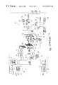
- the computer system 10includes a processor 12 having a processor bus 14 coupled through a memory controller 18 and system memory bus 22 to three packetized or synchronous link dynamic random access memory (“SLDRAM”) devices 16 a-c .
- the computer system 10also includes one or more input devices 20 , such as a keypad or a mouse, coupled to the processor 12 through a bus bridge 22 and an expansion bus 24 , such as an industry standard architecture (“ISA”) bus or a peripheral component interconnect (“PCI”) bus.
- ISAindustry standard architecture
- PCIperipheral component interconnect
- the input devices 20allow an operator or an electronic device to input data to the computer system 10 .
- One or more output devices 30are coupled to the processor 12 to display or otherwise output data generated by the processor 12 .
- the output devices 30are coupled to the processor 12 through the expansion bus 24 , bus bridge 22 and processor bus 14 .
- Examples of output devices 24include printers and a video display units.
- One or more data storage devices 38are coupled to the processor 12 through the processor bus 14 , bus bridge 22 , and expansion bus 24 to store data in or retrieve data from storage media (not shown). Examples of storage devices 38 and storage media include fixed disk drives floppy disk drives, tape cassettes and compact-disk read-only memory drives.
- the processor 12sends a data transfer command via the processor bus 14 to the memory controller 18 , which, in turn, communicates with the memory devices 16 a-c via the system memory bus 22 by sending the memory devices 16 a-c command packets that contain both control and address information.
- Datais coupled between the memory controller 18 and the memory devices 16 a-c through a data bus portion of the system memory bus 22 .
- datais transferred from the SLDRAMs 16 a-c over the memory bus 22 to the memory controller 18 which, in turn, transfers the data over the processor 14 to the processor 12 .
- the processor 12transfers write data over the processor bus 14 to the memory controller 18 which, in turn, transfers the write data over the system memory bus 22 to the SLDRAMs 16 a-c .
- the computer system 10also includes a number of other components and signal lines that have been omitted from FIG. 1 in the interests of brevity.
- the memory devices 16 a-calso receive a master clock signal to provide internal timing signals, a data clock signal clocking data into and out of the memory device 16 , and a FLAG signal signifying the start of a command packet.
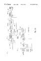
- a typical command packet CA ⁇ 0 : 39 > for an SLDRAMis shown in FIG. 2 and is formed by 4 packet words CA ⁇ 0 : 9 >, each of which contains 10 bits of data. As will be explained in more detail below, each packet word CA ⁇ 0 : 9 > is applied on a command address bus CA including 10 lines CA 0 -CA 9 .
- the four packet words CA ⁇ 0 : 9 > comprising a command packet CA ⁇ 0 : 39 >are designated PW 1 -PW 4 .
- the first packet word PW 1contains 7 bits of data identifying the packetized DRAM 16 a-c that is the intended recipient of the command packet.
- each of the packetized DRAMsis provided with a unique ID code that is compared to the 7 ID bits in the first packet word PW 1 .
- the packetized DRAMs 16 a-cwill receive the command packet, only the packetized DRAM 16 a-c having an ID code that matches the 7 ID bits of the first packet word PW 1 will respond to the command packet.
- the remaining 3 bits of the first packet word PW 1 as well as 3 bits of the second packet word PW 2comprise a 6 bit command. Typical commands are read and write in a variety of modes, such as accesses to pages or banks of memory cells.
- the remaining 7 bits of the second packet word PW 2 and portions of the third and fourth packet words PW 3 and PW 4comprise a 20 bit address specifying a bank, row and column address for a memory transfer or the start of a multiple bit memory transfer. In one embodiment, the 20-bit address is divided into 3 bits of bank address, 10 bits of row address, and 7 bits of column address.
- the command packet shown in FIG. 2is composed of 4 packet words PW 1 -PW 4 each containing up to 10 bits, it will be understood that a command packet may contain a lesser or greater number of packet words, and each packet word may contain a lesser or greater number of bits.
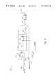
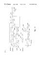
- the memory device 16 ais shown in block diagram form in FIG. 3 .
- Each of the memory devices 16 a-cincludes a clock generator circuit 40 that receives a command clock signal CCLK and generates a large number of other clock and timing signals to control the timing of various operations in the memory device 16 a .
- the memory device 16 aalso includes a command buffer 46 and an address capture circuit 48 which receive an internal clock signal ICLK, a command packet CA ⁇ 0 : 9 > on a 10 bit command-address bus CA, and a terminal 52 receiving a FLAG signal.
- a memory controller (not shown) or other devicenormally transmits the command packet CA ⁇ 0 : 9 > to the memory device 16 a in synchronism with the command clock signal CCLK.
- the command packetwhich generally includes four 10-bit packet words PW 1 -PW 4 , contains control and address information for each memory transfer.
- the FLAG signalidentifies the start of a command packet, and also signals the start of an initialization sequence.
- the command buffer 46receives the command packet from the command-address bus CA, and compares at least a portion of the command packet to identifying data from an ID register 56 to determine if the command packet is directed to the memory device 16 a or some other memory device 16 b, c . If the command buffer 46 determines that the command is directed to the memory device 16 a , it then provides the command to a command decoder and sequencer 60 .
- the command decoder and sequencer 60generates a large number of internal control signals to control the operation of the memory device 16 a during a memory transfer.
- the address capture circuit 48also receives the command packet from the command-address bus CA and outputs a 20-bit address corresponding to the address information in the command packet.
- the addressis provided to an address sequencer 64 , which generates a corresponding 3-bit bank address on bus 66 , a 10-bit row address on bus 68 , and a 7-bit column address on bus 70 .
- the row and column addressesare processed by row and column address paths, as will be described in more detail below.
- the SLDRAM 16 a shown in FIG. 3largely avoids this problem by using a plurality of memory banks 80 , in this case eight memory banks 80 a-h . After a read from one bank 80 a , the bank 80 a can be precharged while the remaining banks 80 b-h are being accessed. Each of the memory banks 80 a-h receives a row address from a respective row latch/decoder/driver 82 a-h .
- All of the row latch/decoder/drivers 82 a-hreceive the same row address from a predecoder 84 which, in turn, receives a row address from either a row address register 86 or a refresh counter 88 as determined by a multiplexer 90 .
- a predecoder 84which, in turn, receives a row address from either a row address register 86 or a refresh counter 88 as determined by a multiplexer 90 .
- only one of the row latch/decoder/drivers 82 a-his active at any one time as determined by bank control logic 94 as a function of a bank address from a bank address register 96 .
- the column address on bus 70is applied to a column latch/decoder 100 , which supplies I/O gating signals to an I/O gating circuit 4102 .
- the I/O gating circuit 4102interfaces with columns of the memory banks 80 a-h through sense amplifiers 104 .
- Datais coupled to or from the memory banks 80 a-h through the sense amps 104 and I/O gating circuit 4102 to a data path subsystem 108 which includes a read data path 110 and a write data path 112 .
- the read data path 110includes a read latch 120 that stores data from the I/O gating circuit 4102 . In the memory device 16 a shown in FIG. 3, 64 bits of data are stored in the read latch 120 .
- the read latchthen provides four 16-bit data words to an output multiplexer 122 that sequentially supplies each of the 16-bit data words to a read FIFO buffer 124 .
- Successive 16-bit data wordsare clocked into the read FIFO buffer 124 by a clock signal RCLK generated from the internal clock signal ICLK.
- the 16-bit data wordsare then clocked out of the read FIFO buffer 124 by a clock signal obtained by coupling the RCLK signal through a programmable delay circuit 126 .
- the programmable delay circuit 126is programmed during initialization of the memory device 16 a so that the data from the memory device is received by a memory controller, processor, or other device (not shown in FIG. 3) at the proper time.
- the FIFO buffer 124sequentially applies the 16-bit data words to a driver circuit 128 which, in turn, applies the 16-bit data words to a data bus DQ forming part of the processor bus 14 (see FIG. 1 ).
- the driver circuit 128also applies one of two data clock signals DCLK 0 and DCLK 1 to respective data clock lines 132 and 133 .
- the data clocks DCLK 0 and DCLK 1enable a device, such as the processor 12 , reading the data on the data bus DQ to be synchronized with the data.
- Particular bits in the command portion of the command packet CA 0 -CA 9determine which of the two data clocks DCLK 0 and DCLK 1 is applied by the driver circuit 128 .
- the data clocks DCLK 0 and DCLK 1are differential clock signals, each including true and complementary signals, but for ease of explanation, only one signal for each clock is illustrated and described.
- the write data path 112includes a receiver buffer 140 coupled to the data bus 130 .
- the receiver buffer 140sequentially applies 16-bit data words from the data bus DQ to four input registers 142 , each of which is selectively enabled by a signal from a clock generator circuit 144 .
- the clock generator circuit 144generates these enable signals responsive to the selected one of the data clock signals DCLK 0 and DCLK 1 .
- the memory controller or processordetermines which data clock DCLK 0 or DCLK 1 will be utilized during a write operation using the command portion of a command packet applied to the memory device 16 a .
- the memory controller or other devicenormally transmits the data to the memory device 16 a in synchronism with the selected one of the data clock signals DCLK 0 and DCLK 1 .
- the clock generator 144is programmed during initialization to adjust the timing of the clock signal applied to the input registers 142 relative to the selected one of the data clock signals DCLK 0 and DCLK 1 so that the input registers 142 can capture the write data at the proper times.
- the input registers 142In response to the selected data clock DCLK 0 or DCLK 1 , the input registers 142 sequentially store four 16-bit data words and combine them into one 64-bit data word applied to a write FIFO buffer 148 .
- the write FIFO buffer 148is clocked by a signal from the clock generator 144 and an internal write clock WCLK to sequentially apply 64-bit write data to a write latch and driver 150 .
- the write latch and driver 150applies the 64-bit write data to one of the memory banks 80 a-h through the I/O gating circuit 4102 and the sense amplifiers 104 .
- the command packet CA ⁇ 0 : 39 >is normally transmitted to the memory device 16 a in synchronism with the command clock signal CCLK, and the data is normally transmitted to the memory device 16 a in synchronism with the selected one of the data clock signals DCLK 0 and DCLK 1 .
- the command packet CA ⁇ 0 : 39 >may not arrive at the memory device 16 a in synchronism with the command clock signal CCLK, and the data may not arrive at the memory device 16 a in synchronism with the selected data clock signal DCLK 0 or DCLK 1 .
- these signalsmay loose synchronism once they are coupled to circuits within the memory device.
- Loss in synchronismmay result from a variety of factors, including temperature variations in the environment in which the SLDRAM 16 a is operating, or drift in operating parameters of components within the SLDRAM 16 a .
- the command clock CCLK and data clocks DCLK 0 and DCLK 1must occasionally be resynchronized to ensure synchronism is maintained.
- the command clock signal CCLKis synchronized when the timing of the internal clock signal ICLK relative to the command clock signal CCLK causes packet words CA ⁇ 0 : 9 > to be latched at the optimum time.
- the phases of a plurality of internal clock signalsare adaptively adjusted where each respective internal clock signal causes a corresponding signal to be stored responsive to the respective internal clock signal.
- a system embodying the present inventionmay include a plurality of clock control circuits, each controlling the phase of a respective internal clock signal relative to a corresponding external clock signal in response to a respective phase command signal.
- At least one evaluation circuitis coupled to latches that are corresponding signals responsive to respective internal clock signals.
- Each evaluation circuitis adapted to receive a plurality of signals sequentially stored in the corresponding latch and generate a results signal indicating whether each of the signals has an expected value.
- a phase selector circuitoperates in a storage mode to sequentially develop a plurality of phase command signals on an output and store corresponding result signals sequentially received on an input.
- the phase selector circuitfurther operates in an analysis mode to develop on the output a final phase command signal determined from the stored result signals.
- a plurality of storage circuitsare coupled to respective clock control circuits and to the output of the phase selector circuit. Each storage circuit stores the final phase command signal responsive to a corresponding clock domain signal.
- a clock-domain control circuitis adapted to receive a synchronization signal. When the synchronization signal is active, the clock-domain control circuit sequentially applies the result signals generated by respective evaluation circuits to the phase selector circuit and develops the clock domain signals to store the resulting final phase command signals in the corresponding storage circuits.
- the clock-domain control circuitfurther operates when the synchronization signal goes inactive before final phase command signals have been determined for each internal clock signal to, when the synchronization signal again goes active, sequentially apply result signals such that final phase command signals are determined only for those internal clock signals not synchronized during the previous cycle of the synchronization signal.
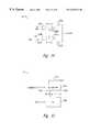
- FIG. 1is a block diagram of a conventional computer system using a plurality of SLDRAM packetized memory devices.
- FIG. 2is diagram showing a typical command packet received by the SLDRAMs of FIG. 1 .
- FIG. 3is a block diagram of a conventional packetized DRAM used in the computer system of FIG. 1 .
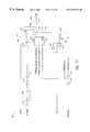
- FIG. 4is block diagram of a partial resynchronization circuit usable in each of the SLDRAMs of FIG. 3 according to one embodiment of the present invention.
- FIG. 5is a schematic of the clock-domain control circuit of FIG. 4 according to one embodiment of the present invention.
- FIG. 6is a more detailed block diagram of one embodiment of the initialization sequencer of FIG. 4 .
- FIG. 7is a schematic of one embodiment of the strobe generator of FIG. 6 .
- FIG. 8is a schematic of one embodiment of the phase compare counter of FIG. 10 .
- FIG. 9is a schematic of one embodiment of the compare control circuit of FIG. 6 .
- FIG. 10is a schematic of one embodiment of the multiplexer of FIG. 6 .
- FIG. 11is a schematic of one embodiment of the pattern generator clocking circuit of FIG. 6 .
- FIG. 12is a more detailed block diagram of an embodiment of one of the variable-phase clock generation circuits of FIG. 4 .
- FIG. 13is a more detailed block diagram of an embodiment of one of the evaluation circuits of FIG. 4 .
- FIG. 14is a more detailed block diagram of one embodiment of the compare circuit of FIG. 13 .
- FIG. 15is more detailed block diagram of an embodiment of the multiplexers of FIG. 4 .
- FIG. 16is a detailed schematic of an embodiment of one of the phase select latches of FIG. 4 .
- FIG. 4is a schematic block diagram of a partial resynchronization circuit 410 according to one embodiment of the present invention.
- the partial resynchronization circuit 410is contained in the command buffer 46 and the clock generation circuit 40 of the SLDRAM 16 a and synchronizes external clock signals CCLK, DCLK 0 , and DCLK 1 during an initialization mode of the SLDRAM 16 a , as will be explained in more detail below.
- Components and signals that were previously described with reference to FIG. 3have been given the same designations in FIG. 4, and will not be described in further detail.
- the partial resynchronization circuit 410includes three variable-phase clock generation circuits 418 , 419 , and 423 , (FIG. 4B) that generate internal clock signals ICLK, IDCLK 0 , and IDCLK 1 , respectively.
- the clock generation circuit 418which is part of the clock generation circuit 40 of FIG. 3, generates the internal command clock signal ICLK in response to the command clock signal CCLK.
- the phase of the internal command clock signal ICLK relative to the command clock signal CCLKis controlled by a phase command CCMDPH ⁇ 0 : 3 > applied to the clock generation circuit 418 .
- the clock generation circuit 419generates the internal data clock signal IDCLK 0 having a phase relative to the data clock signal DCLK 0 that is determined by a phase command DOCMDPH ⁇ 0 : 3 >
- the clock generation circuit 423generates the clock signal IDCLK 1 having a phase relative to the clock signal DCLK 1 that is determined by a phase command DICMDPH ⁇ 0 : 3 >.
- the resynchronization circuit 410determines the optimum values for the phase commands CCMDPH ⁇ 0 : 3 >, DOCMDPH ⁇ 0 : 3 >, and DICMDPH ⁇ 0 : 3 >, as will be explained in more detail below.
- the partial resynchronization circuit 410includes command packet circuitry 411 (FIG. 4A) comprising a shift register 412 receiving command packets CA ⁇ 0 : 39 > applied on the command-address bus CA.
- the width of the command-address bus CAcorresponds to the width of the shift register 412
- the number of packet words CA ⁇ 0 : 9 > in the command packet CA ⁇ 0 : 39 >corresponds to the number of stages of the shift register 412 .
- the shift register 412has four stages, each of which is 10 bits wide. Thus, the shift register 412 sequentially receives four 10-bit packet words CA ⁇ 0 : 9 >.
- Each of the four packet words CA ⁇ 0 : 9 >is shifted into the shift register 412 , and from one shift register stage to the next, responsive to each transition of the internal clock signal ICLK.
- the shift register 412also latches the FLAG signal applied on the flag line 52 coincident with each packet word CA ⁇ 0 : 9 >.
- the FLAG signaltransitions high for one-half of the period of the internal clock signal ICLK.
- the shift register 412shifts high FLAG signal through each of the four stages of the shift register 412 responsive to each transition of the ICLK signal.
- the latched high FLAG signalis used to generate a plurality of control signals as it is shifted through stages of the shift register 412 .
- the shift registergenerates a command trigger signal CTRIGGER.
- a storage register 414loads the 44 bit contents of the shift register 412 .
- the storage register 414receives and stores a 40-bit command word C ⁇ 0 : 39 >, and a 4 bit flag-latched word FLAT ⁇ 0 : 3 >.
- the shift register 412has N+1 stages, each of which has a width of M bits, and the storage register 414 loads an M*N bit command word. After the storage register 414 has been loaded, it continuously outputs the 40 bit command word C ⁇ 0 : 39 > and 4 bit flag-latched word FLAT ⁇ 0 : 3 >.
- the initialization mode of the SLDRAM 16 ais signaled by a FLAG signal that is twice the width of the normal FLAG signal, i.e., a FLAG signal having a duration equal to the period of the ICLK signal.
- the shift register 412activates a calibration signal CAL, causing the resynchronization circuit 410 to execute an initialization procedure to synchronize the CCLK, DCLK 0 , and DCLK 1 clock signals, as will be explained in more detail below.
- the shift register 412once again generates the CTRIGGER signal after four packet words CA ⁇ 0 : 9 > are shifted into the shift register 412 .
- the storage register 414again loads the latched command packet CA ⁇ 0 : 39 > and flag latched word FLAT ⁇ 0 : 3 >.
- shift register 412that may be utilized in the resynchronization circuit 410 is described in more detail in U.S. patent application Ser. No. 08/994,461 to Manning, which is incorporated herein by reference.
- the detailed circuitry of the shift register 412will not be discussed in further detail since such circuitry and operation is slightly tangential to the present invention.
- the shift register 412must be capable a latching packet words CA ⁇ 0 : 9 > received at very high rates during operation of the resynchronization circuit 410 , and during normal operation of the memory device 16 a containing the circuit 410 .
- the command clock CCLKhas a frequency of 200 MHz, requiring the shift register circuit 412 to store one packet word CA ⁇ 0 : 9 > every 2.5 ns (i.e., one packet word in response to each falling and rising edge of the CCLK signal).
- the partial resynchronization circuit 410further includes an evaluation circuit 420 receiving the command word C ⁇ 0 : 39 > and the flag-latched word FLAT ⁇ 0 : 3 > from the storage register 414 .
- the evaluation circuit 420further receives an initialization strobe signal INITSTRB, enable calibration signal ENCAL, and synchronization sequence word SYNCSEQ ⁇ 0 : 3 > generated by an initialization sequencer 430 (FIG. 4 B), and a command initialization signal CINIT developed by a clock-domain control circuit 422 .
- the clock-domain control circuit 422 and initialization sequencer 430generate a plurality of control signals to control operation of the resynchronization circuit 410 .
- the evaluation circuit 420compares each bit of the captured command word C ⁇ 0 : 39 > and flag-latched word FLAT ⁇ 0 : 3 > to expected values determined by the SYNCSEQ ⁇ 0 : 3 > word and generates a command initialization results signal CINITRES in response to these comparisons.
- the evaluation circuit 20drives the CINITRES signal high, indicating the command packet CA ⁇ 0 : 39 > and latched FLAG bits were successfully captured.
- the evaluation circuit 420drives the CINITRES signal inactive low, indicating the command packet CA ⁇ 0 : 39 > and latched FLAG bits were not successfully captured.
- the partial resynchronization circuit 410further includes data packet circuitry 424 (FIG. 4A) that operates in a manner analogous to the command packet circuitry 411 in capturing and evaluating data packet words D ⁇ 0 : 15 > applied on the data bus DQ.
- An input buffer 426transfers data packet words D ⁇ 0 : 15 > received on the data bus DQ to the input registers 142 , which latch the sequentially applied data packet words D ⁇ 0 : 15 > in response to a clock signal applied by a multiplexer 421 .
- the multiplexer 421applies either an internal data clock signal IDCLK 0 or an internal data clock signal IDCLK 1 to the input registers 142 in response to a select clock signal SELCLK generated by the time-domain control circuit 422 (FIG. 4 B).
- the IDCLK 0 and IDCLK 1 clock signalsare internal data clock signals generated by the variable-phase clock generation circuits 419 and 423 , respectively, in response to the respective data clocks DCLK 0 and DCLK 1 , as will be explained in more detail below.
- each data word D ⁇ 0 : 15 >includes 16 bits, which is the width of the data bus DQ.
- the write buffer 148stores and outputs 64 bits of data as a data word D ⁇ 1 : 60 > and a data word D 0 L ⁇ 3 : 0 >.
- the data word D 0 L ⁇ 3 : 0 >corresponds to the four bits of data sequentially latched on the DQO line of the data bus DQ
- the data word D ⁇ 1 : 60 >corresponds to the other 60 bits of data latched on the lines DQ 1 -DQ 15 of the data bus DQ during the latching of the data packets.
- the data word D 0 L ⁇ 3 : 0 >is analogous to the flag-latched word FLAT ⁇ 0 : 3 >, and the function of both of these words will be described in more detail below.
- An evaluation circuit 428receives the D ⁇ 1 : 60 > and D 0 L ⁇ 3 : 0 > data words from the write buffer 148 and operates in a manner analogous to that previously described for the evaluation circuit 420 to compare these captured bits to expected data determined by the SYNCSEQ ⁇ 0 : 3 > word generated by the initialization sequencer 30 .
- the evaluation circuit 28develops a data initialization results signal DINITRES indicating whether each of the bits in the D ⁇ 1 : 60 > and D 0 L ⁇ 3 : 0 > words have their expected values.
- the evaluation circuit 428activates the DINITRES signal, and deactivates this signal when any of these bits does not have its expected value.
- the evaluation circuit 428receives the INITSTRB and ENCAL signals and SYNCSEQ ⁇ 0 : 3 > word from the initialization sequencer 430 , and also receives an enable signal ⁇ overscore (ENABLE) ⁇ generated by a NOR gate 32 in response to D 0 INIT and D 1 INIT signals generated by the clock-domain control circuit 422 .
- the NOR gate 432drives the ⁇ overscore (ENABLE) ⁇ signal active low, which, in turn, activates the evaluation circuit 428 .
- a multiplexer 446receives the CINITRES or DINITRES signals output by the evaluation circuits 420 and 428 , respectively, and the CTRIGGER and LDCD signals. In response to the CINIT signal, the multiplexer 446 applies one of the CINITRES and DINITRES signals on a first output and one of the CTRIGGER or LDCD signals on a second output. When the CINIT signal is active high, the multiplexer 446 applies the CINITRES and CTRIGGER signals on its first and second outputs, respectively, if the CINIT signal is inactive low, the multiplexer 446 applies the DINITRES and LDCD signals on its respective first and second outputs.
- An initialization phase selector 436receives either the CINITRES or DINITRES signal output by the multiplexer 446 .
- the initialization phase selector 436further receives the CAL signal, a latch results signal LATRES, and a phase signal PHASEOK generated by the initialization sequencer 30 .
- a multiplexer 438applies either the ICLK signal generated by the variable-phase clock generation circuit 418 or the WCLK signal generated by the clock generator 40 (see FIG. 3) to clock the initialization phase selector 436 .
- the multiplexer 438applies the ICLK signal to clock the initialization phase selector 436 when the CINIT signal is active high, and applies the WCLK signal when the CINIT signal is inactive low.
- the initialization phase selector 436develops an initialization phase word INITPH ⁇ 0 : 3 >, a phase select done signal PHSELDONE, and a phase ready signal PHREADY, which are applied to a number of components in the partial resynchronization circuit 410 as shown.
- This initialization phase word INITPH ⁇ 0 : 3 >is applied to the inputs of three phase select latches 440 , 442 , and 444 receiving the CINIT, D 0 INIT, and D 1 INIT signals, respectively.
- phase select latches 440 - 444operates in either a transfer mode or a storage mode in response to the corresponding one of the CINIT, D 0 INIT, and D 1 INIT signals output by the clock-domain control circuit 422 .
- the phase select latches 440 - 444each operate in the same way in response to the corresponding signals, and thus, for the sake of brevity, only the operation of the phase select latch 440 will now be described in more detail.
- the phase select latch 440operates in the transfer mode when the CINIT signal is active high.
- the phase select latch 440In the transfer mode, the phase select latch 440 outputs the current value of the INITPH ⁇ 0 : 3 > word as the phase command CCMDPH ⁇ 0 : 3 > to the variable-phase clock generation circuit 418 , and latches the INITPH ⁇ 0 : 3 > word present on its input in response to the PHSELDONE signal going active high.
- the phase select latch 440When the CINIT signal goes inactive low, the phase select latch 440 operates in the storage mode, outputting the latched value of INITPH ⁇ 0 : 3 > word as the phase command CCMDPH ⁇ 0 : 3 > to the clock generation circuit 418 .
- the operation of the initialization phase selector 436 in determining the optimum phase command CCMDPH ⁇ 0 : 3 >, D 0 CMDPH ⁇ 0 : 3 >, or D 1 CMDPH ⁇ 0 : 3 > for the one of the clock signals CCLK, DCLK 0 , and DCLK 1 being synchronized by the resynchronization circuit 410will now be described in more detail before describing the overall operation of the resynchronization circuit 410 .
- One procedure that may be executed by the initialization phase selector 436 in determining each of these optimum phase commandsis described in U.S.
- the initialization phase selector 436operates in two modes in determining each optimum phase command, namely a load mode and an analysis mode.
- the initialization phase selector 436sequentially increments the initialization phase word INITPH ⁇ 0 : 3 > to sequentially increment the phase of the one of the clock signals ICLK, D 0 CLK, or D 1 CLK being synchronized.
- the CINIT signalis active high indicating the CCLK clock signal is being synchronized.
- the phase select latch 440applies INITPH ⁇ 0 : 3 > word as the phase command CCMDPH ⁇ 0 : 3 > to the clock generator 418 .
- the clock generation circuit 418sequentially increments the phase of the ICLK signal.
- the shift register 412attempts to accurately capture each initialization command packet responsive to the respective internal clock signals ICLK that sequentially vary in their timing relationship to the initialization command packets.
- the initialization phase selector 436stores or load values for the CINITRES signal developed by the evaluation circuit 420 at corresponding phases of the ICLK signal.
- the initialization phase selector 436stores a value for the CINITRES signal at each value of the phase command CCMDPH ⁇ 0 : 3 >, and identifies which phase commands CMDPH ⁇ 0 : 3 > caused ICLK to clock the shift register 12 at the proper time to successfully capture these initialization command packets (i.e., which phase commands resulted in a binary 1 for the CINITRES signal).
- the initialization phase selector 436evaluates the stored values for the CINITRES signals at each value of the phase command CCMDPH ⁇ 0 : 3 >. More specifically, a single phase command CMDPH ⁇ 0 : 3 > that is most likely to be able to successfully capture packet words in an initialization command packet is selected from all the phase commands CCMDPH ⁇ 0 : 3 > that successfully captured the initialization command packets. This selected phase command CMDPH ⁇ 0 : 3 > is the command that is thereafter latched by the phase select latch 440 and applied to the clock generation circuit 418 to generate the ICLK signal during normal operation.
- the partial resynchronization circuit 410In operation, when the SLDRAM 16 a containing the partial resynchronization circuit 410 operates in the initialization mode, which is initiated by the FLAG signal going active high for one cycle of the ICLK signal, the partial resynchronization circuit 410 synchronizes the CCLK, DCLK 0 , and DCLK 1 clock signals, as will now be explained in more detail.
- the partial resynchronization circuit 410operates in two submodes, a power-up synchronization submode and a partial synchronization submode.
- the power-up synchronization submodeis initiated by a reset signal ⁇ overscore (RESET) ⁇ going active low, which typically occurs, for example, upon power-up of the computer system 10 (see FIG.
- REETreset signal
- the clock-domain control circuit 422drives the CINIT, D 0 INIT, D 1 INIT, and SO signals inactive low, and the memory controller (FIG. 1) applies a 15-bit repeating pseudo-random bit sequence on each line of the command-address bus CA, data bus DQ, and on line 52 receiving the FLAG signal.
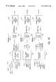
- the 15-bit repeating pseudo-random synchronization bit sequence applied on these linesis shown in Table 1 below.
- the 15-bit pseudo-random bit sequenceis complemented on adjacent lines of the command-address bus CA and data bus DQ.
- the sequencestarts with 0000 on line CA ⁇ 9 >, 1111 on CA ⁇ 8 >, 0000 on CA ⁇ 7 >, and so on such that the sequence applied on each line is the complement of the sequence applied on adjacent lines.
- the partial resynchronization circuit 410places the SLDRAM 16 a in the synchronization mode of operation. More specifically, as shown in Table 1,the pseudo-random bit sequence begins with consecutive 1's for the FLAG signal. As previously described, in response to two consecutive 1's latched for the FLAG signal, the shift register 12 activates the CAL signal to place the partial resynchronization circuit 410 in the initialization mode of operation.
- the clock-domain control circuit 422When the CAL signal goes active high, the clock-domain control circuit 422 initially activates the CINIT signal and maintains the SO, D 0 INIT, and D 1 INIT signals inactive low.
- the multiplexer 446applies the CINITRES signal to the initialization phase selector 436 and the CTRIGGER signal to the initialization sequencer 430 .
- the phase select latch 440in response to the active high CINIT signal, applies the initialization phase word INITPH ⁇ 0 : 3 > output by the initialization phase selector 436 as the phase command CCMDPH ⁇ 0 : 3 > to the variable-phase clock generation circuit 418 .
- the multiplexer 38applies the ICLK signal to clock the initialization phase selector 436 in response to the active CINIT signal.
- the partial resynchronization circuit 410synchronizes the ICLK signal.
- the initialization phase selector 436outputs an initialization phase word INITPH ⁇ 0 : 3 > through the phase select latch 440 as the phase command CCMDPH ⁇ 0 : 3 > to the variable-phase clock generation circuit 418 .
- the clock generation circuit 418In response to the phase command CCMDPH ⁇ 0 : 3 >, the clock generation circuit 418 generates the ICLK signal having an initial phase relative to the CCLK signal that corresponds to the phase command CCMDPH ⁇ 0 : 3 >.
- the shift register 412then latches four packet words CA ⁇ 0 : 9 > applied on the command-address bus CA in response to the ICLK signal. After four packet words CA ⁇ 0 : 9 > have been latched, the shift register 412 outputs the latched command word C ⁇ 0 : 39 > along with the flag-latched word FLAT ⁇ 0 : 3 > to the storage register 414 and generates the CTRIGGER pulse. In response to the CTRIGGER pulse, the storage register 414 latches and outputs the command word C ⁇ 0 : 39 > and flag-latched word FLAT ⁇ 0 : 3 >.
- the evaluation circuit 420receives the latched C ⁇ 0 : 39 > and FLAT ⁇ 0 : 3 > words, and compares these words to expected values determined by the SYNCSEQ ⁇ 0 : 3 > word from the initialization sequencer 430 .
- the initialization sequencer 430generates the SYNCSEQ ⁇ 0 : 3 > word in response to the FLAT ⁇ 0 : 3 > word, as will be described in more detail below.
- the evaluation circuit 420compares the latched command word C ⁇ 0 : 39 > and flag-latched word FLAT ⁇ 0 : 3 > to their expected values determined by the SYNCSEQ ⁇ 0 : 3 > word and activates the CINITRES signal when these words have their expected values.
- the evaluation circuit 420drives the CINITRES signal inactive, indicating the capture of these words at the current phase of the ICLK signal was unsuccessful.
- the CINITRES signalis applied through the multiplexer 446 to the input of the initialization phase selector 436 , which latches the value of the CINITRES signal in response to the LATRES signal developed by the initialization sequencer 430 .
- the initialization sequencer 430pulses the LATRES signal once for every eight comparisons made by the evaluation circuit 420 as long as the CINITRES signal is active high. In this way, for a given phase of the ICLK signal, eight command packets CA ⁇ 0 : 39 > may be latched and subsequently compared by the evaluation circuit 420 to their corresponding expected values as long as the CINITRES signal remains active high. After the eighth comparison, the initialization sequencer 430 pulses the LATRES signal causing the initialization phase selector 436 to latch the CINITRES signal.
- the evaluation circuit 20detects the error and drives the CINITRES signal inactive low. As soon as the CINITRES signal goes inactive low, the initialization sequencer 430 pulses the LATRES signal causing the initialization phase selector 436 to latch the low CINITRES signal. Thus, if all command packets are captured successfully, eight command packets will be captured at a given phase of the ICLK signal and a high CINITRES signal, indicating successful capture of the command packets, will be stored by the initialization phase selector 436 .
- the initialization phase selector 436latches the value of the CINITRES signal in response to the LATRES pulse. In addition, the initialization phase selector 436 also increments the value of the initialization phase word INITPH ⁇ 0 : 3 > in response to the pulsed LATRES signal. This new value of the INITPH ⁇ 0 : 3 > word is once again applied through the phase select latch 440 to the clock generation circuit 18 and corresponds to the new phase of the ICLK signal that is applied to the shift register 412 and used in latching packet words CA ⁇ 0 : 9 > applied on the command-address bus CA.
- the latched command packet CA ⁇ 0 : 39 >is applied to the evaluation circuit 420 , which compares each bit of the latched command packet to an expected value determined by the SYNCSEQ ⁇ 0 : 3 > word. In response to this comparison, the evaluation circuit 20 once again develops the CINITRES signal having a value indicating whether the command packet CA ⁇ 0 : 39 > was successfully captured.
- the initialization phase selector 436operates as previously described in latching a value for the CINITRES signal indicating whether command packets were successfully captured at the new phase of the ICLK signal.
- the initialization phase selector 436After latching a value for the CINITRES signal, the initialization phase selector 436 again increments the value of the INITPH ⁇ 0 : 3 > word which, once again, is applied through the phase select latch 440 as the phase command CCMDPH ⁇ 0 : 3 > to the clock generation circuit 418 which, in turn, generates the ICLK signal having a new phase relative to the ICLK signal. This process is repeated until the initialization phase selector 436 has stored a predetermined number of values for the CINITRES signal, each value corresponding to a different phase of the ICLK signal that was utilized in latching command packets CA ⁇ 0 : 39 > supplied on the command-address bus CA.
- the initialization phase selector 436latches 16 values of the CINITRES signal. In other words, 16 different phases of the ICLK signal are utilized to capture command packets CA ⁇ 0 : 39 > applied on the command-address bus CA.
- the selectorAfter the initialization phase selector 436 has stored 16 values for the CINITRES signal, the selector operates in the analysis mode to determine which of the 16 phases for the ICLK signal will be utilized to capture command packets CA ⁇ 0 : 39 > applied to the SLDRAM 16 a during normal operation. Recall, for each phase of the ICLK signal that successfully captured command packets CA ⁇ 0 : 39 >, the initialization phase selector 436 stored a binary 1 for the CINITRES signal. A binary 0 was stored for the CINITRES signal for all phases of the ICLK signal where the command packets were not successfully captured. Thus, the initialization phase selector 436 selects one of the phases for the ICLK signal that resulted in a binary 1 for the CINITRES signal.
- the initialization phase selector 436After having determined the optimum phase for the ICLK signal, the initialization phase selector 436 outputs the initialization phase word INITPH ⁇ 0 : 3 > corresponding to this phase, and activates the PHSELDONE signal. In response to the active PHSELDONE signal, the phase select latch 440 latches the initialization phase word INITPH ⁇ 0 : 3 > corresponding to the optimum phase for the ICLK signal.
- phase select latch 440thereafter continuously outputs this value as the phase command word CCMDPH ⁇ 0 : 3 > to the clock generation circuit 418 , which generates the ICLK signal having the corresponding phase.
- the phase select latch 440actually does not output the latched initialization phase word INITPH ⁇ 0 : 3 > until the clock-domain control circuit 422 deactivates the CINIT signal, which occurs shortly after the phase selector 436 activates the PHSELDONE signal, as will be described in more detail below.
- the clock-domain control circuit 422deactivates the CINIT signal, indicating an optimum phase for the ICLK signal has been determined and the synchronization of the CCLK signal is therefore completed.
- the clock-domain control circuit 422activates the D 0 INIT signal indicating the DCLK 0 signal will now be synchronized.
- the phase select latch 442places the initialization phase word INITPH ⁇ 0 : 3 > output by the initialization phase selector 436 on its output as the phase command D 0 CMDPH ⁇ 0 : 3 > to the variable-phase clock generation circuit 419 .
- the multiplexer 446applies the DINITRES signal to the initialization phase selector 436 and the LDCD signal to clock the initialization sequencer 430 .
- the multiplexer 438applies the clock signal WCLK to clock the phase selector 436 in response to the low CINIT signal.
- the SELCLK signalgoes active causing the multiplexer 421 to apply the clock signal IDCLK 0 to clock the input registers 142 , and in this way the IDCLK 0 signal is utilized to capture data packets placed on the data bus DQ.
- the NOR gate 432also activates the ENABLE signal in response to the active D 0 INIT signal to thereby enable the evaluation circuit 428 .
- the initialization phase selector 436thereafter operates as previously described to latch 16 values for the DINITRES signal developed in response to corresponding phases of the IDCLK 0 signal, and then determines the optimum value for the phase command D 0 CMDPH ⁇ 0 : 3 > to be applied to the variable-phase clock generation circuit 419 .
- the selectoragain generates the PHSELDONE pulse.
- clock-domain control circuit 422deactivates the D 0 INIT signal and activates the D 1 INIT signal, indicating synchronization of the IDCLK 0 signal has been completed and synchronization of the IDCLKl signal will now begin.
- the NOR gate 432maintains the ⁇ overscore (ENABLE) ⁇ signal applied to the evaluation circuit 428 active in response to the active high D 1 INIT signal.
- the evaluation circuit 428 and initialization phase selector 436thereafter operate identically to the manner previously described for synchronization of the IDCLK 0 signal in determining the optimum phase command D 1 CMDPH ⁇ 0 : 3 > to be applied to the variable phase clock generation circuit 423 and thus, will not be described in further detail.
- the selector 436Once the initialization phase selector 436 has determined the optimum phase command D 1 CMDPH ⁇ 0 : 3 > to synchronize the IDCLK 1 signal, the selector once again generates the PHSELDONE pulse. In response to the PHSELDONE pulse, the clock-domain control circuit 422 deactivates the D 1 INIT signal and activates the SO signal, indicating all three clock signals, ICLK, IDCLK 0 , and IDCLK 1 , have now been synchronized.
- the active high SO signalis typically applied as the SI signal to another SLDRAM and enables initialization and synchronization of the next SLDRAM to begin.
- the resynchronization circuit 410synchronizes all three of the clock signals ICLK, IDCLK 0 , and IDCLK 1 .
- the clock-domain control circuit 422operates in the partial synchronization submode.
- the resynchronization circuit 410synchronizes only those clock signals not synchronized during the previous active cycle of the CAL signal.
- the resynchronization circuit 410enters the partial synchronization submode when the shift register 412 activates the CAL signal in response to the FLAG signal going high for one period of the ICLK signal.
- the clock-domain control circuit 422develops the CINIT, D 0 INIT, and D 1 INIT signals so that the clock signals ICLK, DCLK 0 , and DCLK 1 may be partially synchronized during a single active cycle of the CAL signal, meaning less than all the clock signals may be synchronized during a given synchronization cycle, and only those clock signals not synchronized during the previous active cycle of the CAL signal are then synchronized during a subsequent synchronization cycle or cycles.
- the CAL signalgoes active and the resynchronization circuit 410 begins synchronizing the clock signals ICLK, IDCLK 0 , and IDCLK 1 .
- the CAL signalgoes inactive low after the circuit 410 has synchronized the ICLK signal (i.e., after new phase command CCMDPH ⁇ 0 : 3 > for the ICLK signal has been determined), but before the DCLK 0 signal has been synchronized (i.e., before the phase command D 0 CMDPH ⁇ 0 : 3 > has been determined).
- the clock-domain control circuit 422activates the D 0 INIT signal so that synchronization begins with the IDCLK 0 signal.
- the ICLK signalis not again synchronized since it was successfully synchronized during the previous cycle.
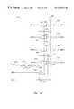
- FIG. 5is a schematic of the clock-domain control circuit 422 according to one embodiment of the present invention.
- the clock-domain control circuit 422sequentially activates the CINIT, D 0 INIT, and D 1 INIT signals in response to a number of signals to control synchronization of the three clock domains defined by the clock signals CCLK, DCLK 0 , and DCLK 1 , as will now be explained in more detail.
- the clock-domain control circuit 422includes a NOR gate 2000 having its output coupled through series connected inverters 2002 and 2004 to develop the CINIT signal.
- the CAL signalis applied through an inverter 206 to a first input of the NOR gate 2000 , and a register 2008 applies its output to a second input of the NOR gate 2000 .
- the clock-domain control circuit 422further includes registers 2010 and 2012 , with the registers 2008 - 2012 having their inputs and outputs coupled in series between a supply voltage source V cc and an input of an inverter 2018 .
- a NAND gate 2022has its output coupled through an inverter 2023 to develop the D 0 INIT signal.
- the NAND gate 2022receives the output of the register 2008 on a first input, the CAL signal on a second input, the output of a NAND gate 2014 on a third input, and the output of the register 2012 coupled through the inverter 2018 on a fourth input. If all these inputs are high, the NAND gate 2022 drives its output low and the inverter 2023 , in turn, drives the D 0 INIT signal active high.
- the NAND gate 2014has its output coupled through an inverter 2016 to develop the D 1 INIT signal in response to the output of the inverter 2018 , the CAL signal, and the output of the register 2010 applied on respective inputs. When all these inputs are high, the NAND gate 2014 drives its output low causing the inverter 2016 to drive the D 1 INIT signal active high.
- a pulse generator 2024applies its output directly and through an inverter 2026 to clock the registers 2008 - 2012 .
- the pulse generator 2024receives the PHSELDONE signal on its input and generates a positive pulse of a fixed duration on its output in response to the falling-edge transition of the PHSELDONE signal.
- the PHSELDONE signalis generated by the initialization phase selector 436 (FIG. 4) whenever the phase selector has determined the optimum phase for the clock domain currently being synchronized.
- the registers 2008 - 2012are reset in response to an output of a positive-edge delay circuit 2032 .
- the registers 2008 - 2012are conventional registers that drive their outputs low in response to the signals on their reset terminals going active low, and circuitry for implementing the function of these registers is well understood by those skilled in the art.
- a NAND gate 2028applies its output through an inverter 2030 to the input of the positive-edge delay circuit 2032 .
- the positive-edge delay circuit 2032drives its output high a predetermined time after a positive edge transition on the output of the inverter 2030 , and drives its output low without such a delay in response to a falling-edge transition on the output of the inverter 2030 .
- the NAND gate 2028receives three inputs and whenever one or more of these inputs goes inactive low the NAND gate 2028 drives its output high resetting the registers 2008 - 2012 .
- the positive-edge delay circuit 2032ensures that the reset signal applied to the registers 2008 - 2012 stays active low for at least its delay time, even if the output of the NAND gate 2028 remains high for a shorter duration.
- a NAND gate 2034applies its output to one input of the NAND gate 2028 , and receives the inverted CAL signal from the inverter 2006 on a first input and the output of the register 2012 on a second input.
- the NAND gate 2034applies a low output to the NAND gate 2028 which, in turn, drives its output high resetting the registers 2008 - 2010 .
- a NOR gate 2036applies its output through an inverter 2038 to a second input of the NAND gate 2028 .
- the NOR gate 2036receives the CAL signal on a first input and a never calibrated signal ⁇ overscore (NEVCAL) ⁇ on a second input.
- the ⁇ overscore (NEVCAL) ⁇ signalis generated by an RS flip-flop 2004 including cross-coupled NAND gates 2042 and 2044 .
- the NOR gate 2036drives its output high causing the inverter 2038 to apply a low signal to the NAND gate 2028 which, in turn, drives its output high resetting the registers 2008 - 2012 .
- a NAND gate 2046applies its output to an inverter 2048 which, in turn, applies an internal reset signal ⁇ overscore (IRESET) ⁇ to the final input of the NAND gate 2028 .
- the NAND gate 2046receives a reset signal ⁇ overscore (RESET) ⁇ and power up signal ⁇ overscore (PWRUP) ⁇ on respective inputs, and drives its output high when either of the signals goes active low.
- the inverter 2048drives the ⁇ overscore (IRESET) ⁇ signal active low causing the NAND gate 2028 to drive its output high, resetting the registers 2008 - 2012 .
- the clock-domain control circuit 422further includes an inverter 2050 that develops the select output signal SO in response to the output from a NAND gate 2052 .
- the SO signalgoes active high once all three clock domains CCLK, DCLK 0 , and DCLK 1 have been successfully synchronized.
- the NAND gate 2052receives the ⁇ overscore (NEVCAL) ⁇ signal on a first input, a select input signal SI on a second input, and the output from a NAND gate 2054 on a third input. When all of its inputs are high, the NAND gate 2052 applies a low output to the inverter 2050 which, in turn, activates the SO signal.
- NVCAL⁇ overscore
- the RS flip-flop 2040develops the ⁇ overscore (NEVCAL) ⁇ signal in response to an output of a NAND gate 2056 applied on its set input and the ⁇ overscore (IRESET) ⁇ signal from the inverter 2048 applied on its reset input.
- IRESET⁇ overscore
- the RS flip-flop 2040latches the ⁇ overscore (NEVCAL) ⁇ signal active low.
- the RS flip-flop 2040latches the ⁇ overscore (NEVCAL) ⁇ signal inactive high to enable the NAND gate 2052 when the NAND gate 2056 drives its output low, which occurs when both the output of the register 2012 and the SI signal are high.
- the NAND gate 2054drives its output high, enabling the NAND gate 2052 when either of respective outputs from NAND gates 2058 and 2060 is low.
- the NAND gate 2058is enabled by the CAL signal, and receives a current calibration done signal ⁇ overscore (CCD) ⁇ from an RS flip-flop 2062 including cross-coupled NAND gates 2064 and 2066 .
- the RS flip-flop 2062receives a set input from the NAND gate 2056 , the ⁇ overscore (IRESET) ⁇ signal on a first reset input, and a second reset input from a pulse generator 2068 and applied through an inverter 2070 .
- the CAL signalis applied through an inverter 2072 to the input of the pulse generator 2068 , which generates a positive pulse having a fixed duration in response to a falling-edge transition on the output of the inverter 2072 .
- the RS flip-flop 2062is reset, latching the CCD signal inactive low when either the CAL signal goes active high or the ⁇ overscore (IRESET) ⁇ signal goes active low.
- the RS flip-flop 2062latches the CCD signal active high when the output of the NAND gate 2056 goes low.
- the NAND gate 2060receives the CAL signal applied through the inverter 2006 and the output of an RS flip-flop 2074 including cross-coupled NAND gates 2076 and 2078 .
- An identification valid signal IDVALIDis applied through an inverter 2080 to the set input of the RS flip-flop 2074 , and the inverter 2048 applies the reset input to the RS flip-flop 2074 .
- the ⁇ overscore (IRESET) ⁇ signalgoes active low, the RS flip-flop 2074 latches its output low, and thereafter, in response to an active high IDVALID signal, the inverter 2080 outputs an active low set input causing the RS flip-flop 2074 to latch its output high.
- the RS flip-flop 2074maintains its output high until reset by the ⁇ overscore (INTRES) ⁇ signal going active low, which does not occur during normal operation of the clock-domain control circuit 422 . Once the RS flip-flop 2074 has been set, this output enables the NAND gate 2060 which then drives its output low and high responsive to the CAL signal going low and high, respectively.
- INTRES⁇ overscore
- the clock-domain control circuit 422operates in one of two modes, a reset mode and synchronization mode.
- the reset mode of operationis characterized by one or both of the ⁇ overscore (RESET) ⁇ and ⁇ overscore (PWRUP) ⁇ signals going active low which, in turn, drives the ⁇ overscore (IRESET) ⁇ signal active low.
- circuitry(not shown in FIG. 20) drives the CAL and IDVALID signals inactive low.
- the NAND gate 2028drives its output high resetting the registers 2008 - 2012 such that each register drives its corresponding output low.
- the NAND gates 2022 and 2014drive their respective outputs high deactivating the D 0 INIT and D 1 INIT signals.
- the NOR gate 2000drives its output low deactivating the CINIT signal.
- the low ⁇ overscore (IRESET) ⁇ signalresets the RS flip-flops 2040 , 2062 , and 2074 which, in turn, disable the NAND gates 2052 , 2058 , and 2060 respectively.
- the disabled NAND gate 2052drives its output high deactivating the SO signal.
- the clock-domain control circuit 422resets the registers 2008 - 2012 and the RS flip-flops 2040 , 2062 , 2074 , and also deactivates all of the CINIT, D 0 INIT, D 1 INIT, and SO signals.
- the clock-domain control circuit 422sequentially activates the CINIT, D 0 INIT, and D 1 INIT signals in response to the PHSELDONE signal, and thereafter activates the SO signal once all three clock domains have been synchronized, as will now be explained in more detail.
- the clock-domain control circuit 422operates in two submodes during the synchronization mode, an initial synchronization submode and a partial synchronization submode.
- the clock-domain control circuit 422operates in the initial synchronization submode immediately after operation in the reset mode, and thereafter operates in the partial synchronization submode. After operating in the reset mode, the clock-domain control circuit 422 enters the initial synchronization submode in response to circuitry (not shown in FIG.
- the high IDVALID signalsets the RS flip-flop 2074 , enabling the NAND gate 2060 .
- the high SI signalenables the NAND gate 2056 and also enables the NAND gate 2052 to operate responsive to the signals applied on its other two inputs.
- the NOR gate 2000drives its output high activating the CINIT signal.
- the high CAL signalenables a number of components within the clock-domain control circuit 422 , and also causes the pulse generator 2068 to generate a pulse that resets the RS flip-flop 2062 if that flip-flop was previously set.
- this pulse generated by the pulse generator 2068has no effect on the RS flip-flop 2062 since that flip-flop has just been reset during the reset mode.
- the generation of the pulse by the pulse generator 2068 in response to the CAL signal going highwill be described in more detail below with reference to the partial synchronization submode of operation.
- the clock-domain control circuit 422applies the active high CINIT signal to a variety of components within the partial resynchronization circuit 410 (FIG. 4) and that circuit operates as previously described to synchronize the ICLK signal.
- the initialization phase selector 436pulses the PHSELDONE signal.
- the pulse generator 2024In response to the falling edge of the PHSELDONE pulse, the pulse generator 2024 generates a pulse that clocks the registers 2008 - 2012 , shifting the high signal applied on the input of the register 2008 to the output of that register.
- the NOR gate 2000drives its output low deactivating the CINIT signal.
- the NAND gate 2022whose other three inputs were already high, drives its output low activating the D 0 INIT signal.
- the partial resynchronization circuit 410In response to the D 0 INIT signal going high, the partial resynchronization circuit 410 (FIG. 4) synchronizes the IDCLK 0 signal as previously described.
- the initialization phase selector 436determines the optimum initialization phase word INITPH ⁇ 0 : 3 > to synchronize the IDCLK 0 signal
- the phase selectorgenerates the PHSELDONE pulse.
- the pulse generator 2024once again clocks the registers 2008 - 2012 , shifting the high on the input of the register 2010 to the output of that register.
- the NAND gate 2014whose other two inputs are already high, drives its output low activating the D 1 INIT signal.
- the NAND gate 2022drives its output high deactivating the D 0 INIT signal.
- the partial resynchronization circuit 410(FIG. 4) operates as previously described to synchronize the IDCLK 1 signal and, once the signal has been synchronized, the initialization phase selector 436 (FIG. 4) applies the PHSELDONE pulse to the pulse generator 2024 .
- the pulse generator 2024In response to the PHSELDONE pulse, the pulse generator 2024 once again clocks the registers 2008 - 2012 , shifting the high on the output of the register 2010 to the output of the register 2012 .
- the inverter 2018applies a low to the NAND gate 2014 which, in turn, drives its output high deactivating the D 1 INIT signal.
- the NAND gate 2056Further in response to the output of the register 2012 going high, the NAND gate 2056 , which now receives two high inputs, drives its output low causing the RS flip-flop 2040 to latch the ⁇ overscore (NEVCAL) ⁇ signal high and the RS flip-flop 2062 to latch the CCD signal high.
- the NAND gate 2058In response to the CCD signal going high, the NAND gate 2058 , which now receives two high inputs, drives its output low causing the NAND gate 2054 to apply a high output to the NAND gate 2052 . At this point, all three inputs of the NAND gate 2052 are high, and the NAND gate 2052 accordingly drives its output low activating the SO signal which indicates all three clock domains have now been successfully synchronized.
- the high output from the register 2012also enables the NAND gate 2034 which, while the CAL signal remains active high, maintains its output high.
- the inverter 2006drives its output high causing the NAND gate 2034 to drive its output low.
- the NAND gate 2028drives its output high, resetting the registers 2008 - 2012 , in anticipation of the next active cycle of the CAL signal.
- the clock-domain control circuit 422continues operating in the initial synchronization submode until successfully synchronizing all three clock domains during a single active cycle of the CAL signal, which may hereinafter be referred to as a synchronization cycle.
- the registers 2008 - 2012are reset causing the clock-domain control circuit 422 to commence operation during the next active cycle of the CAL signal by again first activating the CINIT signal such that the partial resynchronization circuit 410 (FIG. 4) again starts by synchronizing the ICLK clock signal first.
- the clock-domain control circuit 422nonetheless starts the next active cycle of the CAL signal by again synchronizing the ICLK signal.
- the RS flip-flop 2040latches the ⁇ overscore (NEVCAL) ⁇ signal active low until reset by a low output from the NAND gate 2056 , which occurs in response to a high output from the register 2012 indicating all three clock domains have been successfully synchronized.
- the ⁇ overscore (NEVCAL) ⁇ signalis applied to one input of the NOR gate 2036 and the CAL signal is applied to the other input of this NOR gate.
- the NOR gate 2036drives this output low, causing the inverter 2038 to apply a high signal to the NAND gate 2028 .
- the NOR gate 2036When the CAL signal goes low before the RS flip-flop 2040 has set the ⁇ overscore (NEVCAL) ⁇ signal high, the NOR gate 2036 receives two low inputs once the CAL signal does go low. In response to these two low inputs, the NOR gate 2036 drives its output high causing the inverter 2038 to apply a low signal to the NAND gate 2028 which, in turn, drives its output high resetting the registers 2008 - 2012 as previously described. In other words, before the RS flip-flop 2040 is set to latch the ⁇ overscore (NEVCAL) ⁇ signal high, every time the CAL signal goes low, the NOR gate 2036 drives its output high which results in the registers 2008 - 2012 being reset.
- the clock-domain control circuit 422operates in the partial synchronization submode.
- the clock-domain control circuit 422synchronizes only those clock domains not successfully synchronized during the previous active cycle or cycles of the CAL signal. For example, during the partial synchronization submode, if the ICLK clock domain was successfully synchronized and the partial resynchronization circuit 410 (FIG.
- the clock-domain control circuit 422did not again synchronize the ICLK clock domain but instead starts by synchronizing the IDCLK 0 clock domain. In this way, the clock-domain control circuit 422 does not unnecessarily resynchronize clock domains synchronized during previous active cycles of the CAL signal.
- the clock-domain control circuit 422during the partial synchronization submode will now be described in more detail. For the following description, it is assumed that the initial synchronization submode has just synchronized the three clock signals ICLK, IDCLK 0 and IDCLK 1 during the previous active cycle of the CAL signal. At this point, when the CAL signal goes active, the clock-domain control circuit 422 commences operation in the partial synchronization submode.
- the operation of the clock-domain control circuit 422is identical to that previously described during the initial synchronization submode, except that the RS flip-flop 2040 has already latched the ⁇ overscore (NEVCAL) ⁇ signal inactive high.
- the registers 2008 - 2102are not reset so that during the next active cycle of the CAL signal, the partial resynchronization circuit 410 (FIG.
- the clock-domain control circuit 422begins synchronizing the clock domain that was in the process of being synchronized during the previous active cycle of the CAL signal but which was not successfully synchronized during that cycle. For example, assume that the CAL signal goes active, placing the clock-domain control circuit 422 in the partial synchronization submode. Further assume that the ICLK signal has been successfully synchronized and that the partial resynchronization circuit 410 is in the process of synchronizing the IDCLK 0 signal. As previously described, when the IDCLK 0 signal is being synchronized, the clock-domain control circuit 422 activates the D 0 INIT signal and deactivates the CINIT, D 1 INIT, and SO signals. At this point, the output of the register 2008 is high while the outputs of the registers 2010 and 2012 are low.
- the high ⁇ overscore (NEVCAL) ⁇ signaldisables the NOR gate 2036 so that it maintains its output low when the CAL signal goes low.
- the inverter 2038maintains its output high and does not, as previously described, go low causing the NAND gate 2028 to drive its output high to reset the registers 2008 - 2012 .
- the output of the register 2012is at this point low, and this low output disables the NAND gate 2034 , which maintains its output high when the CAL signal goes low.
- the registers 2008 - 2012are not reset.
- the low CAL signalis also applied to the NAND gate 2022 .
- the NAND gate 2022drives its output high deactivating the D 0 INIT signal which, in turn, disables synchronization of the IDCLK 0 signal currently being executed by the partial resynchronization circuit 410 (FIG. 4 ).
- the CAL signalis applied directly to the NAND gates 2022 and 2014 , and through the inverter 2006 to the NOR gate 2000 , disabling all these gates when it is low.
- the associated one of these gatesdeactivates that signal in response to the low CAL signal.
- the initialization phase selector 436also receives the CAL signal and resets itself in response to that signal going inactive low.
- the synchronization of the IDCLK 0starts over at the beginning and the initialization phase selector 436 must again store 16 DINITRES signals, each corresponding to a particular phase of the IDCLK 0 signal, and thereafter select the optimum phase as previously described.
- the initialization phase selector 436starts at the beginning and stores a new value for the first stored DINITRES signal.
- the clock-domain control circuit 422repeats this process as many times as required to synchronize all three of the clock domains ICLK, IDCLK 0 and IDCLK 1 .
- the registers 2008 - 2012are reset as previously described so that during the next synchronization cycle, the clock-domain control circuit 422 activates the CINIT signal to again start by synchronizing the ICLK signal.
- the register 2016latches its output high enabling the NAND gate 2034 so that next time the CAL signal goes low, the NAND gate 2034 drives its output low causing the NAND gate 2028 to drive its output high which, in turn, resets the registers 2008 - 2012 .
- the partial synchronization submode of operationreduces the time required for the clock-domain control circuit 422 to synchronize all three clock domains when the synchronization cycle is interrupted before synchronization of all three domains is complete. Referring back to FIG. 1, this allows the memory controller 18 to synchronize the SLDRAMs 16 a- 16 c , each containing the partial resynchronization circuit 410 , while the computer system 10 is in operation.
- the memory controller 18may initiate a synchronization cycle and thereafter, in response to, for example, a data request from the processor 12 , may then terminate the synchronization cycle, retrieve the requested data, and transfer that data to the processor 12 .
- the memory controller 18may once again initiate a synchronization cycle and the partial resynchronization circuits 410 in the SLDRAMs 16 a- 16 c being synchronized thereafter synchronize only those clock domains not synchronized during the previous synchronization cycle.
- FIG. 6is a more detailed functional block diagram of the initialization sequencer 430 .
- the initialization sequencer 430includes an initialization strobe generator 2100 that generates a plurality of control signals in response to either the CTRIGGER or LDCD signals output by the multiplexer 446 .
- the CTRIGGER pulseis generated after the four packet words CA ⁇ 0 : 9 > applied on the command-address bus CA have been latched and stored in the storage register 414 (FIG.
- the multiplexer 446outputs the CTRIGGER signal when the ICLK signal is being synchronized and the LDCD pulse when either of the IDCLK 0 or IDCLK 1 signals is being synchronized.
- a phase compare counter 2104is clocked by the initialization strobe generator 2100 and develops a three bit phase compare count S ⁇ 0 : 2 > indicating the number of comparisons performed by the evaluation circuits 420 , 428 (FIG. 4) at a given phase of the clock domain being synchronized.
- a compare control circuit 2106receives the phase compare count S ⁇ 0 : 2 > and the one of the CINITRES or DINITRES signals corresponding to the clock domain currently being synchronized. In the following description, it is assumed to ICLK signal is being synchronized, so the CINITRES signal is applied to the compare control circuit 2106 .
- the compare control circuit 2106applies the latched results pulse LATRES to the initialization phase selector 436 (FIG. 4 ), causing the initialization phase selector 436 to latch the value of the CINITRES signal.
- the compare control circuit 2106generates the LATRES pulse when either the CINITRES signal is inactive low, or the count S ⁇ 0 : 2 > equals 111.
- the compare control circuit 2106generates the LATRES pulse after eight successful comparisons at a given phase of the clock domain being synchronized, or when the CINITRES signal indicates an unsuccessful comparison.
- the compare control circuit 2106deactivates the ENCAL signal applied to the evaluation circuits 420 and 428 (FIG. 4) to thereby reset these evaluation circuits in anticipation of evaluating packet words CA ⁇ 0 : 9 > captured at the next phase of the clock domain being synchronized.
- the compare control circuit 2106also outputs the phase signal PHASEOK signal to the phase compare counter 2104 and initialization strobe generator 2100 .
- the compare control circuit 2106deactivates the PHASEOK signal when either the count S ⁇ 0 : 2 > equals 111 or the CINITRES signal goes low.
- phase compare counter 2104In response to the PHASEOK signal going low, the phase compare counter 2104 resets the count S ⁇ 0 : 2 > to 000 and generates a count reset pulse ⁇ overscore (CNTREST) ⁇ indicating comparisons of packet words captured at a given phase of the clock domain being synchronized are complete. In addition, the low PHASEOK signal disables the initialization strobe generator 2100 until that signal again goes active high.
- the initialization sequencer 430further includes a pattern generator 2108 receiving either the flag-latched word FLAT ⁇ 0 : 3 > or latched word D 0 L ⁇ 0 : 3 > from a multiplexer 2110 , and utilizes the applied word to develop the synchronization sequence word SYNCSEQ ⁇ 0 : 3 >.
- the SYNCSEQ ⁇ 0 : 3 > wordis applied to the evaluation circuits 420 and 428 (FIG. 4) to determine the expect data for these circuits.
- the multiplexer 2110applies the FLAT ⁇ 0 : 3 > word when the ICLK clock domain is being synchronized, and otherwise applies the D 0 L ⁇ 0 : 3 > word when either the IDCLK 0 or IDCLK 1 clock domains are being synchronized.
- a pattern generator clocking circuit 2112clocks the pattern generator 2108 with a pair of complementary seed clock signals SCLK, ⁇ overscore (SCLK) ⁇ , and also applies a seed signal SEED to the pattern generator 2108 .
- the pattern generator 2108utilizes the FLAT ⁇ 0 : 3 > or D 0 L ⁇ 0 : 3 > word output by the multiplexer 2110 to develop the synchronization sequence word SYNCSEQ ⁇ 0 : 3 > which, as previously described, is applied to the evaluation circuits 420 and 428 (FIG. 4) to determine expect data for these circuits.
- the pattern generator clocking circuit 2112is controlled by the initialization strobe generator 2100 and reset in response to the ⁇ overscore (CNTRESET) ⁇ signal generated by the phase compare counter 2104 .
- the pattern generator 2108may be a conventional pattern recognition circuit which, upon receiving the FLAT ⁇ 0 : 3 > or D 0 L ⁇ 0 : 3 > word equal to 1111, thereafter generates the predetermined sequence of values defined by the repeating 15 bit pseudo-random bit sequence applied on FLAG, CA, and DQ lines (see Table 1). In other words, the pseudo-random bit sequences starts with 1111 applied for the FLAG bit. The next four FLAG bits that are captured, one coincident with each packet word CA ⁇ 0 : 9 >, are 0101, followed by 1001, and so on as seen in Table 1.
- the pattern generator 2108merely starts generating the expected values 0101, 1001, and so on for the SYNCSEQ ⁇ 0 : 3 > word after receiving the FLAT ⁇ 0 : 3 > or DOC ⁇ 0 : 3 > word equal to 1111.
- circuitrythat may be utilized to develop the predetermined sequence of SYNCSEQ ⁇ 0 : 3 > words generated by the pattern generator 2108 , such as a state machine formed from appropriate logic circuitry.
- FIG. 7is a more detailed schematic of one embodiment of the initialization strobe generator 2100 of FIG. 6 .
- the initialization strobe generator 2100includes a NAND gate 2200 that develops an active signal ⁇ overscore (ACTIVE) ⁇ on its output in response to either the CTRIGGER or LDCD signal applied on a first input.
- the PHASEOK signalenables the NAND gate 2200 when active high.
- a pulse generator 2202generates a low output pulse having a predetermined duration in response to a falling-edge of the ⁇ overscore (ACTIVE) ⁇ signal.
- the output pulse of the pulse generator 2202is applied through an inverter 2204 to develop a pulse trigger signal PTRIGGER.
- a NAND gate 2206is enabled by an enable initialization strobe signal ENINITSTRB received on a first input, and receives the PTRIGGER signal on a second input. When enabled, the NAND gate 2206 outputs a complementary initialization strobe signal ⁇ overscore (INITSTRB) ⁇ , which is applied through an inverter 2208 to develop an initialization strobe signal INITSTRB.
- a pulse generator 2210generates a negative pulse on its output in response to a falling-edge of the INITSTRB signal, and this output pulse is applied through a first inverter 2212 to develop a pulse initialization strobe signal PINITSRB and through a second inverter 2214 to develop a complementary pulse initialization strobe ⁇ overscore (PINITSTRB) ⁇ .
- the initialization strobe generator 2100is enabled when the PHASEOK and ENINITSTRB signals are active high.
- the NAND gate 2200drives the ⁇ overscore (ACTIVE) ⁇ signal active low in response to the CTRIGGER signal going active high.
- the pulse generator 2202In response to the ⁇ overscore (ACTIVE) ⁇ signal going low, the pulse generator 2202 generates a low pulse on its output which is applied through the inverter 2204 to develop the PTRIGGER signal. In the embodiment of FIG. 7, the pulse generator 2202 generates a 2 nanosecond low pulse so the PTRIGGER signal is accordingly a 2 nanosecond high pulse.
- the NAND gate 2206pulses its output low and thereby develops the INITSTRB, ⁇ overscore (INITSTRB) ⁇ pulses.
- the pulse generator 2210In response to the falling-edge of the INITSTRB pulse, the pulse generator 2210 generates a 1 nanosecond low pulse on its output which is applied through the inverters 2212 and 2214 to develop the PINITSTRB, ⁇ overscore (PINITSTRB) ⁇ pulses.
- the NAND gate 2200when the PHASEOK signal is inactive low, the NAND gate 2200 is disabled, driving the ⁇ overscore (ACTIVE) ⁇ and PTRIGGER inactive high and thereby inhibiting development of the INITSTRB, ⁇ overscore (INITSTRB) ⁇ and PINITSTRB, ⁇ overscore (PINITSTRB) ⁇ signals.
- the ENINITSTRB signalwhen the ENINITSTRB signal is inactive low, the NAND gate 2206 is disabled preventing development of the INITSTRB, ⁇ overscore (INITSTRB) ⁇ and PINITSTRB, ⁇ overscore (PINITSTRB) ⁇ signals.
- FIG. 8is a more detailed schematic of the phase compare counter 2104 of FIG. 6 .
- the phase compare counter 2104includes three registers 2300 - 2304 that develop the respective count bits S ⁇ 0 >, S ⁇ 1 >, and S ⁇ 2 >.
- a NOR gate 2306has its output coupled directly and through an inverter 2308 to clock the registers 2300 - 2304 with complementary clock signals CLK, ⁇ overscore (CLK) ⁇ , which are generated in response to the ⁇ overscore (PINITSTRB) ⁇ pulse received on a first input of the NOR gate 2306 .
- the NOR gate 2306is enabled by a NAND gate 2310 receiving the CAL and PHASEOK signals on respective inputs.
- the output of the NAND gate 2310is further applied through an inverter 2312 which develops a count reset signal ⁇ overscore (CNTRESET) ⁇ to reset the registers 2300 - 2304 when either or both of the CAL and PHASEOK signals go inactive low.
- the count bits S ⁇ 0 >-S ⁇ 2 >are fed back to the inputs of the respective registers 2300 - 2304 in order to cause the counter 2104 to increment its three bit binary count as it is clocked by the clock signals CLK, ⁇ overscore (CLK) ⁇ . Accordingly, the bit S ⁇ 0 > is fed back through an inverter 2304 to the input of the register 2300 .
- An XOR gate 2316receives the bits S ⁇ 0 > and S ⁇ 1 > on the respective inputs and applies its output to the input of the register 2302 .
- An XOR gate 2318applies its output to the input of the register 2304 in response to the S ⁇ 2 > bit applied on a first input and the logical AND of the S ⁇ 0 > and S ⁇ 1 > bits applied to a NAND gate 2320 an output through an inverter 2322 to the second input of the XOR gate 2318 .
- the phase compare counter 2104operates in a conventional manner to increment the count S ⁇ 0 : 2 > from 000 to 111 as the registers 2300 - 2304 are clocked by the CLK, ⁇ overscore (CLK) ⁇ signals.
- CLK⁇ overscore
- the CAL and PHASEOK signalsare active high, causing the NAND gate 2310 to enable the NOR gate 2306 and also causing the inverter 2312 to drive the ⁇ overscore (CNTRESET) ⁇ signal inactive high.
- the CLK, ⁇ overscore (CLK) ⁇ signalsare generated in response to each ⁇ overscore (PINITSTRB) ⁇ pulse and thereby cause the registers 2300 - 2304 to increment the count S ⁇ 0 : 2 > from 000 to 111.
- the NAND gate 2310drives its output high, causing the inverter 2312 to drive the ⁇ overscore (CNTRESET) ⁇ signal active low resetting the count S ⁇ 0 : 2 > to 000.
- the PHASEOK signalgoes inactive low if a particular command or data packet was not successfully captured.
- the phase compare counter 2104resets its count S ⁇ 0 : 2 > to 000 whenever a command or data packet is unsuccessfully captured, in anticipation of comparing 8 command or data packets captured at the next phase of the clock domain being synchronized.
- FIG. 9is a detailed schematic of one embodiment of the compare control circuit 2106 of FIG. 6 .
- a pulse generator 2400generates a low output pulse in response to a falling-edge transition of either the CTRIGGER or LDCD signal, depending upon which of the clock domains is being synchronized.
- the output of the pulse generator 2400is applied through an inverter 2402 to a NAND gate 2404 which is enabled by the PHREADY signal developed by the initialization phase selector 436 (FIG. 4 ).
- the PHREADY signalis developed by the initialization phase selector 436 to allow for settling time of the clock signal being synchronized after adjusting the phase of that clock signal, as will be understood by one skilled in the art.
- An RS flip-flop 2406includes cross-coupled NAND gates 2408 and 2410 and receives the output of the NAND gate 2404 on a set input.
- a NOR gate 2412applies the reset input to the RS flip-flop 2406 in response to the output of an AND gate 2414 applied on a first input and the output of a NAND gate 2416 applied through an inverter 2418 to a second input.
- the AND gate 2414receives the PINITSTRB signal on a first input and either the CINITRES or DINITRES signal applied through an inverter 2420 on a second input.
- the NOR gate 2412drives its output low resetting the RS flip-flop 2406 , which occurs when the PINITSTRB signal is high and the applied one of the CINITRES or DINITRES signals is inactive low.
- the NOR gate 2412also drives its output low, resetting the RS flip-flop 2406 , when the inverter 2418 drives its output high, which occurs when the NAND gate 2416 drives its output low.
- the NAND gate 2416receives the PTRIGGER signal on one input and the count S ⁇ 0 : 2 > output by the phase compare counter 2104 (FIG. 23) on their respective inputs.
- the NAND gate 2416drives its output low causing the inverter 2418 to drive its output high and the NOR gate 2412 , in turn, to drive its output low resetting the RS flip-flop 2406 .
- the output of the RS flip-flop 2406is applied through series connected inverters 2422 , 2424 to generate the PHASEOK signal.
- the output of the inverter 2422is further applied directly to one input of a NAND gate 2426 and indirectly through the delay and pulse generation circuitry 2425 to a second input of the NAND gate 2426 . More specifically, the output of the inverter 2422 is input to a positive-edge delay circuit 2428 that develops a positive-edge transition on its output a predetermined time after receiving a positive-edge transition on its input. In response to a negative-edge transition on its input, the positive-edge delay circuit 2428 develops a negative-edge transition on its output without any such delay.
- the output of the positive-edge delay circuit 2428is applied through an inverter 2430 to an input of a pulse generator 2432 .
- the pulse generator 2432operates as do previously described pulse generators, developing a low pulse on its output in response to a falling-edge transition on its input.
- the output of the pulse generator 2432is applied through three series connected inverters 2434 - 2438 to develop the latched results pulse LATRES.
- the initialization phase selector 436latches the value of either the CINITRES or DINITRES signal present on its input in response to the LATRES pulse.
- the LATRES pulseis also applied to one input of a positive-edge delay circuit 2440 having its other input coupled to the supply voltage V cc .
- the positive-edge delay circuit 2440develops a positive-edge transition on its output a predetermined time after receiving a positive-edge transition of the LATRES pulse, and develops a negative-edge transition on its output without such delay in response to a negative-edge transition of the LATRES pulse.
- a NAND gate 2442is enabled by the CAL signal on a first input and receives the output of a NAND gate 2426 on a second input.
- the output of a NAND gate 2442is coupled through an inverter 2444 to develop the ENCAL signal which, as described above with reference to FIG. 4, enables the evaluation circuits 420 and 428 (FIG. 4) when active high, and resets these circuits when inactive low.
- the NAND gate 2442drives its output low, in response to the output of the NAND gate 2426 going high, and drives its output high in response to the output of the NAND gate 2426 going low.
- compare control circuit 2106receives the CTRIGGER and CINITRES signals, corresponding to the situation when the ICLK clock domain is being synchronized, as previously described above.
- the PHREADY signalis active high
- the falling edge of the CTRIGGER pulsegenerates a low output pulse causing the NAND gate 2404 to drive its output low which, in turn, resets the RS flip-flop 2406 , thereby driving the output of the NAND gate 2408 high.
- the PHASEOK signalgoes active high, and the inverter 2422 applies a low output to the NAND gate 2426 which, in turn, drives its output high.
- the NAND gate 2442receives two high inputs and drives its output low causing the inverter 2444 to activate the ENCAL signal.
- the low output of the inverter 2422does not cause the pulse generator 2432 to generate a low pulse, but instead the pulse generator 2432 drives its output high resulting in the inverter 2438 driving the LATRES signal inactive low.
- the low LATRES signalis applied through the positive-edge delay circuit 2440 to the NAND gate 2426 which, at this point, receives two low inputs.
- the compare control circuit 2106After the RS flip-flop 2406 has been set in response to the falling-edge of the CTRIGGER signal, the compare control circuit 2106 maintains the PHASEOK and ENCAL signals active high, and the LATRES signal inactive low. The compare control circuit 2106 maintains these signal values until one of two events resets the RS flip-flop 2406 .
- the RS flip-flop 2406is reset when the NOR gate 2412 drives its output low, which occurs when either the AND gate 2414 drives its output high or the NAND gate 2416 drives its output low.
- the AND gate 2414drives its output high when the PINITSTRB signal is high and the CINITRES signal is low. As previously described, the CINITRES signal is low when the evaluation circuit 420 (FIG.
- the resulting low CINITRES signalcauses the AND gate 2414 to drive its output high, and the NOR gate 2412 , in turn, to drive its output low resetting the RS flip-flop 2406 .
- the NAND gate 2408drives its output low causing the inverter 2424 to drive the PHASEOK signal inactive low.
- the inverter 2422applies a high input to the NAND gate 2426 .
- the other input of the NAND gate 2426remains low and thus the NAND gate 2422 maintains its output low causing the inverter 2444 to maintain the ENCAL signal active high.
- the positive-edge delay circuit 2428drives its output high after the predetermined delay time, which in one embodiment of a compare control circuit 2106 is 2 nanoseconds.
- the inverter 2430drives its output low causing the pulse generator 2432 to output a low pulse, which has a duration of 3 nanoseconds in one embodiment of the compare control circuit 2106 .
- the inverter 2438drives the LATRES signal active high causing the initialization phase selector 436 (FIG. 4) to latch the value of the CINITRES signal applied on its input, as previously described.
- the positive-edge delay circuit 2440drives its output high the predetermined time later, which is 0.5 nanoseconds in one embodiment of the compare control circuit 2106 .
- the NAND gate 2426receives two high inputs and drives its output low causing the NAND gate 2442 to drive its output high and the inverter 2444 , in turn, to drive the ENCAL signal inactive low.
- the evaluation circuit 420is reset in anticipation of comparing the next captured command packet to the associated expect data.
- the second condition that resets the RS flip-flop 2406occurs when the output of the NAND gate 2416 goes low causing the inverter 2418 to drive its output high and the NOR gate 2412 , in turn, to drive its output low, resetting the RS flip-flop 2406 .
- the NAND gate 2416drives its output low when the PTRIGGER signal is active high, and the compare count S ⁇ 0 : 2 > developed by the phase compare counter (FIG. 21) equals 111. When this occurs, all inputs to the NAND gate 2416 are high, causing it to drive its output low and thereby reset the RS flip-flop 2406 .
- the compare control circuit 2106operates as previously described to deactivate the PHASEOK and ENCAL signals and activate the LATRES signal.
- the PHASEOK and ENCAL signalsare deactivated and the LATRES signal activated when either the compare count S ⁇ 0 : 2 > equals 111, or the CINITRES signal goes low.
- FIG. 10is a more detailed schematic of one embodiment of the multiplexer 2110 of FIG. 6 .
- the multiplexer 2110includes first and second pass gates 2500 and 2502 that operate in a complementary manner to apply either the latched FLAT ⁇ 0 : 3 > or D 0 L ⁇ 3 : 0 > word as a seed word A ⁇ 0 : 3 > to the pattern generator 2108 (FIG. 6 ).
- a NAND gate 2504has its output applied directly and through an inverter 2506 to control the pass gate 2500
- a NAND gate 2508has its output applied directly and through an inverter 2510 to control the pass gate 2502 .
- the CINIT signalis applied directly to a first input of the NAND gate 2504 , and is applied through an inverter 2512 to a first input of the NAND gate 2508 .
- the NAND gates 2504 and 2508are enabled by the CAL signal applied on respective second inputs.
- both NAND gates 2504 and 2508drive their respective outputs high turning off pass gates 2500 and 2502 so that neither the FLAT ⁇ 0 : 3 > or D 0 L ⁇ 3 : 0 > words are output.
- the CAL signalis active high, which of the FLAT ⁇ 0 : 3 > D 0 L ⁇ 3 : 0 > words are output as the seed word A ⁇ 0 : 3 > depends upon the state of the CINIT signal.
- the NAND gate 2504drives its output low turning ON the pass gate 2500 which, in turn, outputs the FLAT ⁇ 0 : 3 > word as the seed word A ⁇ 0 : 3 >.
- the inverter 2512drives its output low causing the NAND gate 2508 to drive its output high which, in turn, turns OFF the pass gate 2502 .
- the NAND gate 2504drives its output high turning OFF the pass gate 2500 and the NAND gate 2508 drives its output low turning ON the pass gate 2502 and thereby coupling the D 0 L ⁇ 3 : 0 > word to its output as the seed word A ⁇ 0 : 3 >.
- the multiplexer 2110when the CINIT signal is active high during synchronization of the ICLK clock domain, the multiplexer 2110 outputs the FLAT ⁇ 0 : 3 > word as the seed word A ⁇ 0 : 3 > to the pattern generator 2108 (FIG. 6 ). If either the IDCLK 0 or IDCLK 1 clock domains are being synchronized, the multiplexer 2110 applies the D 0 L ⁇ 3 : 0 > word as the seed word A ⁇ 0 : 3 > to the pattern generator 2108 .
- FIG. 11is a detailed schematic of one embodiment of the pattern generator clocking circuit 2112 of FIG. 6 .
- the pattern generator clocking circuit 2112includes an RS flip-flop 2600 comprising cross-coupled NAND gates 2602 and 2604 and having its output coupled through an inverter 2608 to develop the SEED signal.
- the SEED signalenables the pattern generator 2108 (FIG. 21) to store either the FLAT ⁇ 0 : 3 > or D 0 L ⁇ 3 : 0 > word output by the multiplexer 2110 .
- a NOR gate 2610has its output coupled through an inverter 2612 to apply a set input to the RS flip-flop 2600 .
- the NOR gate 2610has one input coupled to ground and receives the ⁇ overscore (CNTRESET) ⁇ signal on a second input.
- the NOR gate 2610drives its output high and the inverter 2612 drives its output low, resetting the RS flip-flop 2600 which causes the NAND gate 2604 to drive its output low and the inverter 2608 to drive the SEED signal active high.
- a pulse generator 2614generates a low output pulse that is applied through series connected inverters 2616 and 2618 to the reset input of the RS flip-flop 2600 .
- the pulse generator 2614receives its input from a NAND gate 2620 and generates the low pulse on its output in response to a falling-edge transition on the output of the NAND gate 2620 .
- the inverter 2618drives the reset input low, resetting the RS flip-flop 2600 and thereby causing the NAND gate 2604 to drive its output high and the inverter 2608 to drive the SEED signal inactive low.
- the output of the NAND gate 2602develops the enable initialization strobe signal ENINITSTRB which, when high, enables circuitry in the initialization strobe generator 2100 (FIG. 6 ).
- the pattern generator clocking circuit 2112couples the output of the NAND gate 2620 through inverters 2622 and 2624 to develop the pair of complementary seed clock signals SCLK, ⁇ overscore (SCLK) ⁇ which, as previously described above, clock the pattern generator 2108 (FIG. 6) to generate sequential SYNCSEQ ⁇ 0 : 3 > words as it is clocked, each of the SYNCSEQ ⁇ 0 : 3 > words representing expect data corresponding to a particular captured command or data packet.
- a pulse generator 2626applies a low output pulse through series connected inverters 2628 and 2630 to a first input of the NAND gate 2620 .
- the pulse generator 2626generates the low output pulse in response to a falling-edge transition from a NOR gate 2632 .
- the NOR gate 2632has one input coupled to ground and a second input coupled to the output of an RS flip-flop 2634 including cross-coupled NAND gates 2636 and 2638 .
- the RS flip-flop 2634receives the ⁇ overscore (ACTIVE) ⁇ signal on a set input and the ⁇ overscore (CNTREST) ⁇ signal on a reset input.
- the RS flip-flop 2634is reset, driving the output of the NAND gate 2636 low which, in turn, causes the NOR gate 2632 to drive its output high.
- the RS flip-flop 2634is set in response to the ⁇ overscore (ACTIVE) ⁇ signal going active low, causing the NAND gate 2636 to drive its output high which, in turn, causes the NOR gate 2632 to drive its output low.
- the pattern generator clocking circuit 2112further includes a NAND gate 2640 receiving the ⁇ overscore (INITSTRB) ⁇ signal on a first input and an output from a positive-edge delay circuit 2642 on a second input.
- the positive-edge delay circuit 2642has its input coupled to the output of the inverter 2630 and develops a positive-edge transition on its output a predetermined time after receiving a positive-edge transition on its input, and develops a falling-edge transition on its output in response to a falling-edge transition on its input without such delay.
- the output of the NAND gate 2640is applied to an input of a pulse generator 2644 which develops a low output pulse in response to a falling-edge transition on its input.
- a NAND gate 2646has one input coupled to the supply voltage V cc and a second input coupled to the output of the pulse generator 2644 .
- the pulse generator 2644develops the low pulse on its output
- the NAND gate 2646drives its output high, causing an inverter 2648 to apply a low signal on a second input of the NAND gate 2620 .
- the output of the pulse generator 2644is high
- the NAND gate 2646drives its output low, causing the inverter 2648 to apply a high output to the NAND gate 2620 .
- the pattern generator clocking circuit 2112operates in two modes, a seed mode and an expect data generation mode.
- ⁇ overscore (CNTREST) ⁇ signalhas just pulsed active low, resetting the RS flip-flop 2634 and RS flip-flop 2600 .
- the NAND gate 2604drives its output low, causing the inverter 2608 to drive the SEED signal active high.
- the RS flip-flop 2634is reset, the NAND gate 2636 drives its output low, causing the NOR gate 2632 to drive its output high.
- the pulse generator 2626maintains its output high and this high output is applied through the inverters 2628 and 2630 to the NAND gate 2620 .
- the positive-edge delay circuit 2642applies a high output to the NAND gate 2640 in response to the high output from the inverter 2630 .
- the NAND gate 2640receives two high inputs so its output is low, but it is assumed the pulse generator 2644 has already generated its low output pulse in response to the falling-edge transition from the NAND gate 2640 .
- the pulse generator 2644maintains its output high and the NAND gate 2646 , in turn, drives its output low, causing the inverter 2648 to apply a high output to the NAND gate 2620 .
- the NAND gate 2620likewise also receives two high inputs at this point and accordingly drives its output low, causing the inverters 2622 and 2624 to drive the SCLK signal high and SCLK signal low, respectively.
- the initialization strobe generator 2100(FIG. 6) then drives the ⁇ overscore (ACTIVE) ⁇ and ⁇ overscore (INITSTRB) ⁇ signals active low.
- the NAND gate 2640drives its output high and the pulse generator 2644 maintains its output high in response to this positive-edge transition on its input.
- the RS flip-flop 2634is set, causing the NAND gate 2636 to drive its output high.
- the NOR gate 2632drives its output low, causing the pulse generator 2626 to generate a low pulse on its output.
- This low pulse output by the pulse generator 2626is applied through the inverters 2628 and 2630 to the NAND gate 2620 .
- the NAND gate 2620drives its output high, causing the inverters 2622 and 2624 to clock the SCLK signal low and ⁇ overscore (SCLK) ⁇ high, respectively.
- the positive-edge delay circuit 2642outputs a low to the NAND gate 2640 , which already has a high output in response to the low ⁇ overscore (INITSTRB) ⁇ signal.
- the pulse generator 2626again drives its output high and this high output is applied through the inverters 2628 and 2630 to the input of the NAND gate 2620 .
- the NAND gate 2620again drives its output low, causing the inverters 2622 and 2624 to clock the SCLK signal high and ⁇ overscore (SCLK) ⁇ low, respectively.
- the pattern generator clocking circuit 2112has generated a single SCLK, ⁇ overscore (SCLK) ⁇ clock pulse in response to the ⁇ overscore (ACTIVE) ⁇ signal setting the RS flip-flop 2634 .
- the initialization strobe generator 2100(FIG. 6) drives the ⁇ overscore (INITSTRB) ⁇ signal inactive high.
- the NAND gate 2640which now receives two high inputs, drives its output low.
- the pulse generator 2644generates a low output pulse.
- the NAND gate 2646drives its output high, causing the inverter 2648 to drive its output low.
- the NAND gate 2620receives a high from the inverter 2630 and a low pulse from the inverter 2648 and accordingly drives its output high in response to the low output pulse from the inverter 2648 .
- the inverters 2622 and 2624again drive the SCLK signal low and ⁇ overscore (SCLK) ⁇ high, respectively.
- the NAND gate 2646again drives its output low, causing the inverter 2648 to again apply a high output to the NAND gate 2620 which, in turn, now receives two high inputs and accordingly drives its output low.
- the inverters 2622 and 2624clock the SCLK signal high and the ⁇ overscore (SCLK) ⁇ low, respectively.
- the pattern generator clocking circuit 2112thereafter clocks the SCLK, ⁇ overscore (SCLK) ⁇ signals in response to pulses of the ⁇ overscore (INITSTRB) ⁇ signal. This is true because once the RS flip-flop 2634 is set by the ⁇ overscore (ACTIVE) ⁇ signal going active low, the pulse generator 2626 does not generate another pulse until the RS flip-flop 2634 is first reset by the ⁇ overscore (CNTREST) ⁇ signal and then again set by the ⁇ overscore (ACTIVE) ⁇ signal. Thus, the pulse generator 2626 generates a single pulse in response to the RS flip-flop 2634 being set.
- the NAND gate 2620is enabled by the high output from the inverter 2630 and clocks the SCLK, ⁇ overscore (SCLK) ⁇ signals in response to each pulse generated by the pulse generator 2644 .
- the pulse generator 2644generates a pulse in response to each low transition output by the NAND gate 2640 , which occurs when the low ⁇ overscore (INITSTRB) ⁇ terminates (i.e., when the ⁇ overscore (INITSTRB) ⁇ signal goes high).
- FIG. 12is a functional block diagram of one embodiment of the variable-phase clock generation circuit 418 of FIG. 4 .
- the variable-phase clock generation circuits 418 , 419 , and 423are identical, and thus, for the sake of brevity, only the clock generation circuit 418 will be described in more detail with reference to FIG. 12 .
- the variable-phase clock generation circuit 418includes a delay-locked loop 500 that develops a plurality of clock signals 502 a-n in response to the CCLK signal.
- the clock signals 502 a-nhave phase shifts, designated ⁇ 1 - ⁇ N , respectively, relative to the CCLK signal.
- ⁇ 1 - ⁇ Nphase shifts
- the delay-locked loop 500develops 16 clock signals 502 a-n and maintains a phase shift of 180° between the clock signals 502 a and 502 n .
- the phases of the clock signals 502 a-nincrease in increments of 11.25° from the phase ⁇ 1 to ⁇ 16 .
- the clock signal 502 ahas a phase ⁇ 1 relative to the CCLK signal
- each of the clock signals 502 b-nhas a phase 11.25° greater than the preceding phase such that the clock signal 502 n has the phase ⁇ 16 that is 180° greater than the phase ⁇ 1 .
- the clock signals 502 a-nare applied to respective inputs of a multiplexer 504 that also receives the phase command word CCMDPH ⁇ 0 : 3 >.
- the multiplexer 504couples one of the clock signals 502 a-n to an output and through a buffer 506 to generate the ICCLK signal.
- the value of the phase command word CCMDPH ⁇ 0 : 3 >determines which of the clock signals 502 a-n is used to generate the ICCLK signal and thereby determines the phase of the ICCLK signal relative to the CCLK signal.
- FIG. 13illustrates one embodiment of the evaluation circuit 420 of FIG. 4, which, as previously described, compares the command word C ⁇ 0 : 39 > and flag-latched word FLAT ⁇ 0 : 3 > to expected values determined by the SYNCSEQ ⁇ 0 : 3 > word, and generates the CINITRES signal having a value indicating the result of this comparison.
- the evaluation circuit 420includes a PMOS reset transistor 600 coupled between a supply voltage source V cc and a sensing node 602 and receiving an enable calibration signal ENCAL on its gate.
- a latch 604 including two cross-coupled inverters 606 , 608has its input coupled to the sensing node 602 and its output coupled to an input of an inverter 610 which develops the CINITRES signal on its output in response to the output of the latch 604 .
- the evaluation circuit 420further includes a compare circuit 612 coupled between the sensing node 602 and an enable node 614 .
- the compare circuit 612receives the latched command word C ⁇ 0 : 39 > and flag-latched word FLAT ⁇ 0 : 3 > corresponding to the captured command packet received on the command-address bus CA and latched FLAG bits received on the flag line 52 , as previously described.
- the compare circuit 612further receives a plurality of signals derived from the synchronization sequence word SYNCSEQ ⁇ 0 : 3 > generated by the initialization sequencer 430 .
- each bit of the synchronization sequence word SYNCSEQ ⁇ 0 : 3 >is coupled through an inverter 616 to generate a complementary synchronization sequence word ⁇ overscore (SYNCSEQ) ⁇ 0 : 3 > which, in turn, is further coupled through an inverter 618 to generate a buffered synchronization sequence word SYNCSEQBUF ⁇ 0 : 3 >.
- the ⁇ overscore (SYNCHSEQ) ⁇ 0 : 3 > and SYNCHSEQBUF ⁇ 0 : 3 > wordsare utilized by the compare circuit 612 in determining whether each of the bits in the command word C ⁇ 0 : 39 > and latched FLAG word FLAT ⁇ 0 : 3 > has its expected value, as will be explained in more detail below.
- the evaluation circuit 420further includes an enable transistor 620 coupled between the enable node 614 and ground.
- An inverter 628has its output applied through a transmission gate 622 to the gate of the enable transistor 620 .
- the CINIT signalis applied directly and through an inverter 624 to the control terminals of the transmission gate 622 .
- the output of the inverter 624is further applied to a gate of a transistor 626 coupled between the gate of the enable transistor 620 and ground.
- the inverter 624drives its output low turning OFF the transistor 626 and turning ON the transmission gate 622 and thereby coupling the output of the inverter 628 to the gate of the enable transistor 620 .
- a pulse generator 630provides a pulse signal to the input of the inverter 628 in response to the INITSTRB signal applied through an inverter 632 to its input.
- the inverter 632drives its output low causing the pulse generator 630 to apply a low pulse signal on the input of the inverter 628 , which, in turn, drives its output high for the duration of this pulse.
- This high output from the inverter 628is coupled through the transmission gate 622 , when activated, turning ON the enable transistor 622 .
- the output of the inverter 628is further coupled through an inverter 634 to one input of a NAND gate 636 receiving the ENCAL signal on a second input.
- the output of the NAND gate 636is applied directly and through an inverter 638 to enable terminals of a buffer 640 coupled between the output of the latch 604 and the sensing node 602 as shown.
- the buffer 640is enabled and applies the inverse of the signal on the output of the latch 604 on the sensing node 602 . If the output of the NAND gate 636 is high, the buffer 640 is disabled, placing its output in a high impedance state.
- FIG. 14is a more detailed schematic of the compare circuit 612 of FIG. 13 including a plurality of bit compare circuits BCC 1 -BCCN. There is one bit compare circuit BCC 1 -BCCN for each bit compared by the compare circuit 612 .
- the compare circuit 612includes 44 bit compare circuit BCC 1 -BCC 44 , one for each bit of the command word C ⁇ 0 : 39 > and flag-latched word FLAT ⁇ 0 : 3 >. All the bit compare circuits BCC 1 -BCCN are identical, and thus, for the sake of brevity, only the bit compare circuit BCC 1 will be described in more detail.
- the bit compare circuit BCC 1receives the bit C ⁇ 0 > of the command word C ⁇ 0 : 39 >, and applies this bit through a first inverter 700 to an input of a first transmission gate 702 , an through the first inverter 700 and a second inverter 704 to the input of a second transmission gate 706 .
- the transmission gates 702 and 706receive the ⁇ overscore (SYNCSEQ) ⁇ 0 > and SYNCSEQBUF ⁇ 0 > signals on their respective control terminals as shown, and are activated in a complementary manner in response to the values of these signals.
- the transmission gate 702turns ON and transmission gate 706 turns OFF, and when the signals ⁇ overscore (SYNCSEQ) ⁇ 0 > and SYNCSEQBUF ⁇ 0 > are low and high, respectively, the transmission gate 706 turns ON and transmission gate 702 turns OFF.
- the outputs of the transmission gates 702 and 706are applied to a gate of a comparison transistor 708 coupled between the sensing node 602 and the enable node 614 .
- the bit compare circuit BCC 1compares the value of the bit C ⁇ 0 > to its expected value determined by the values of the bits ⁇ overscore (SYNCSEQ) ⁇ 0 > and SYNCSEQBUF ⁇ 0 > and activates the compare transistor 708 when the bit C ⁇ 0 > does not have its expected value, as will now be explained in more detail.
- the initialization sequencer 430determines an expected value for the command bit C ⁇ 0 > from the latched FLAG word FLAT ⁇ 0 : 3 > as previously mentioned, and as will be discussed in more detail below.
- the ⁇ overscore (SYNCSEQ) ⁇ 0 > and SYNCSEQBUF ⁇ 0 > bitsare driven high and low, respectively, turning ON transmission gate 702 and turning OFF transmission gate 706 .
- the command bit C ⁇ 0 >is then applied through the inverter 700 and through the turned ON transmission gate 702 to the gate of the compare transistor 708 . If the command bit C ⁇ 0 > is high as expected, the inverter 700 applies a low signal through the transmission gate 702 to the gate of the compare transistor 708 , turning OFF this transistor.
- the inverter 700drives its output high and this high output is applied through the transmission gate 702 to the gate of the transistor 708 .
- the transistor 708turns ON, coupling the sensing node 602 to the enable node 614 .
- the ⁇ overscore (SYNCSEQ) ⁇ 0 > and SYNCSEQBUF ⁇ 0 >are driven low and high, respectively, turning ON the transmission gate 706 and turning OFF the transmission gate 702 .
- the command bit C ⁇ 0 >is then applied through the inverters 700 and 704 and through the turned ON transmission gate 706 to the gate of the compare transistor 708 . If the command bit C ⁇ 0 > is a binary 0 as expected, the inverter 704 drives its output low, turning OFF the transistor 708 and isolating the sensing node 602 from the enable node 614 .
- the inverter 704drives its output high, turning ON the transistor 708 which couples the sensing node 602 to the enable node 614 .
- the evaluation circuit 420in comparing the value of each bit in the command word C ⁇ 0 : 39 > and flag-latched word FLAT ⁇ 0 : 3 > to its expected value will now be described in more detail.
- the transmission gate 622turns OFF and the transistor 626 turns ON.
- the turned ON transistor 626couples the gate of the enable transistor to ground, turning OFF the enable transistor 620 which isolates the enable node 614 from ground.
- the evaluation circuit 420is deactivated and does not evaluate the command word C ⁇ 0 : 39 > and flag-latched word FLAT ⁇ 0 : 3 >.
- the evaluation circuit 420is enabled when the CINIT signal is active high turning ON the transmission gate 622 and enable transistor 620 , which couples the enable node 614 to approximately ground.
- the ENCAL signalgoes inactive low before evaluation of a particular command word C ⁇ 0 : 39 > and flag-latched word FLAT ⁇ 0 : 3 >.
- the transistor 600turns ON, coupling the sensing node 602 to approximately the supply voltage V cc .
- the latch 604drives its output low and the inverter 610 , in turn, drives the CINITRES signal on its output high.
- the INITSTRB signalis inactive low and the pulse generator 630 drives its output high causing the inverter 628 to drive its output low.
- the low output from the inverter 628is applied through the turned ON transmission gate 622 to the gate of the enable transistor 620 , turning OFF this transistor and thereby isolating the enable node 614 from ground.
- the ENCAL signalgoes inactive low to reset the evaluation circuit 420 by turning ON the transistor 600 to drive the sensing node 602 to approximately the supply voltage V cc .
- the latch 604drives its output low causing the inverter 610 , in turn, to drive the CINITRES signal active high.
- the NAND gate 636deactivates the buffer 640 enabling the transistor 600 to more easily drive the sensing node 602 high.
- the ENCAL signalthereafter goes active high, enabling the evaluation circuit 420 to begin comparing latched command words C ⁇ 0 : 39 > and flag-latched words FLAT ⁇ 0 : 3 >.
- the synchronization sequence word SYNCSEQ ⁇ 0 : 3 >is applied to the evaluation circuit 420 and the corresponding ⁇ overscore (SYNCSEQ) ⁇ 0 : 3 > and SYNCSEQBUF ⁇ 0 : 3 > words are, in turn, applied to the compare circuit 612 , indicating the expected value for each of the bits in the latched C ⁇ 0 : 39 > and FLAT ⁇ 0 : 3 > words.
- the INITSTRB signalthen goes active high and the pulse generator 630 , in turn, generates the low pulse on its output, causing the inverter 628 to pulse its output high and thereby turn ON the enable transistor 620 so that the compare circuit 612 compares the latched command word C ⁇ 0 : 39 > and flag-latched word FLAT ⁇ 0 : 3 > to the expected data.
- the voltage on the sensing node 602remains high such that the latch 604 maintains its output low and the inverter 610 continues driving the CINITRES signal active high indicating the latched words C ⁇ 0 : 39 > and FLAT ⁇ 0 : 3 > were successfully captured. If any of the bits in the words C ⁇ 0 : 39 > and FLAT ⁇ 0 : 3 > does not have its expected value, the corresponding compare transistor 708 turns ON, coupling the sensing node 602 to approximately ground.
- the latch 604drives its output high causing the inverter 610 to drive the CINITRES signal low, indicating the C ⁇ 0 : 39 > and FLAT ⁇ 0 : 3 > words were not successfully captured.
- the low pulse on the output of the pulse generator 630results in the inverter 634 also pulsing its output low, which causes the NAND gate 636 to drive its output high for the duration of this pulse.
- the buffer 640is disabled to enable the sensing node 602 to be more easily driven low if any of the bits were not successfully captured.
- the NAND gate 636again drives its output low enabling the buffer 640 to drive the sensing node 602 to its desired value.
- the sensing node 602may present a rather large capacitance due to all the components coupled in parallel to this node, and the buffer 640 includes transistors sized such that the buffer may drive this relatively large capacitance to its desired voltage and in this way assists the inverter 606 which typically has smaller sized transistors.
- the multiplexer circuit 446 of FIG. 4includes four transmission gates 802 - 808 receiving the CTRIGGER, LDCD, CINITRES, and DINITRES signals on their inputs, respectively.
- the CINIT signalis applied directly and through an inverter 810 to the control terminals of the transmission gates 802 - 808 as shown.
- the transmission gates 802 and 804operate in a complementary manner to couple either the CTRIGGER or LDCD signal through a pair of series connected inverters 812 and 814 to an output terminal 816 .
- the transmission gates 806 and 808operate in a complementary manner in response to the CINIT signal, coupling either the CINITRES or DINITRES signal through series connected inverters 818 and 820 to an output terminal 822 .
- the multiplexer 446when the CINIT signal is active high, the multiplexer 446 outputs the CTRIGGER and CINITRES signals on the output terminals 816 and 822 , respectively.
- the multiplexer 446When the CINIT signal is inactive low, the multiplexer 446 outputs the LDCD and DINITRES signals on the terminals 816 and 822 , respectively. In this way, the multiplexer 446 applies the CTRIGGER pulse to clock the initialization sequencer 430 (FIG.
- the multiplexer 446applies the LDCD and DINITRES signals to the sequencer 430 and selector 436 , respectively, when either of the data clocks DCLK 0 or DCLK 1 is being synchronized (i.e., CINIT signal is low).
- FIG. 16is a more detailed schematic of the phase select latch 440 of FIG. 4 . All the phase select latches 440 - 444 are identical, and thus, for the sake of brevity, only the latch 440 will be described in more detail with reference to FIG. 16 .
- the INITPH ⁇ 0 : 3 > signalsare applied to respective latch circuits 1600 - 1606 .
- the outputs of the latch circuits 1600 - 1606are applied to respective pass gates 1608 - 1614 which are coupled to respective inverter pairs 1616 - 1622 .
- the latch circuits 1600 - 1606may be selectively bypassed by respective pass gates 1624 - 1630 .
- the pass gates 1608 - 1614 and the pass gates 1624 - 1630are connected to each other so that the pass gates 1608 - 1614 are enabled alternately with the pass gates 1624 - 1630 in response to the CINIT signal applied directly and through an inverter 1638 to the control terminals of these pass gates.
- the CINIT signalhigh, thereby enabling the pass gates 1624 - 1630 directly.
- the latches 1600 - 1606are bypassed in the storage mode so that the phase command INITPH ⁇ 0 : 3 > is applied to the variable-phase clock generation circuit 418 (FIG. 4) to determine the phase of the ICLK signal relative to the CCLK signal.
- the PHSELDONE signalgoes active high.
- the PHSELDONE signalis applied to one input of a NAND gate 1644 , which is enabled by the CINIT signal.
- the NAND gate 1644In response to the active high PHSELDONE signal, the NAND gate 1644 drive its output low, thereby triggering a pulse generator 1642 .
- the pulse generated by the pulse generator 1642is applied through an inverter 1646 to S inputs of the latch circuits 1600 - 1606 , and an inverter 1647 applies the complement of this signal to the S input of the latch circuits 1600 - 1606 .
- the latch circuits 1600 - 1606then store the INITPH ⁇ 0 : 3 > signals that correspond to the optimum phase for the ICLK signal.
- the INITPH ⁇ 0 : 3 > signals stored in the latch circuits 1600 - 1606are then coupled through the inverter pairs 1616 - 1622 by the pass gates 1608 - 1614 and output as the phase command CCMDPH ⁇ 0 : 3 >.
- the latch circuits 1600 - 1606store the CCMDPH ⁇ 0 : 3 > signals until either new CCMDPH ⁇ 0 : 3 > signals are stored in the latch circuits 1600 - 1606 during a synchronization cycle, or they are reset by the ⁇ overscore (RESET) ⁇ signal applied to reset inputs of the latches 1600 , 1602 , and 1606 , and through an inverter 1649 to the set input of the latch 1604 .
- the latchesreset the stored INITPH ⁇ 0 : 3 > signals to 1101 when the ⁇ overscore (RESET) ⁇ signal goes active low.
- the stored CCMDPH ⁇ 0 : 3 >is applied to the clock generator 418 (FIG. 4) to thereby set the phase of the ICLK signal to an optimum value for use in capturing command packets applied on the command-address bus CA.
- the clock generator 418FIG. 4
- a variety of different circuitsmay be utilized to perform the functions of the latches 1600 - 1606 , and such circuits are understood by one skilled in the art.
Landscapes
- Engineering & Computer Science (AREA)
- Theoretical Computer Science (AREA)
- Physics & Mathematics (AREA)
- General Engineering & Computer Science (AREA)
- General Physics & Mathematics (AREA)
- Dram (AREA)
Abstract
Description
| TABLE 1 | |||||||||||||||
| 1 | 1 | 1 | 1 | 0 | 1 | 0 | 1 | 1 | 0 | 0 | 1 | 0 | 0 | 0 | |
| CA<9> | 0 | 0 | 0 | 0 | 1 | 0 | 1 | 0 | 0 | 1 | 1 | 0 | 1 | 1 | 1 |
| CA<8> | 1 | 1 | 1 | 1 | 0 | 1 | 0 | 1 | 1 | 0 | 0 | 1 | 0 | 0 | 0 |
| CA<7> | 0 | 0 | 0 | 0 | 1 | 0 | 1 | 0 | 0 | 1 | 1 | 0 | 1 | 1 | 1 |
| M | M | M | M | M | M | M | M | M | M | M | M | M | M | M | M |
| CA<0> | 1 | 1 | 1 | 1 | 0 | 1 | 0 | 1 | 1 | 0 | 0 | 1 | 0 | 0 | 0 |
| DQ<15> | 0 | 0 | 0 | 0 | 1 | 0 | 1 | 0 | 0 | 1 | 1 | 0 | 1 | 1 | 1 |
| DQ<14> | 1 | 1 | 1 | 1 | 0 | 1 | 0 | 1 | 1 | 0 | 0 | 1 | 0 | 0 | 0 |
| M | M | M | M | M | M | M | M | M | M | M | M | M | M | M | M |
| DQ<0> | 1 | 1 | 1 | 1 | 0 | 1 | 0 | 1 | 1 | 0 | 0 | 1 | 0 | 0 | 0 |
Claims (35)
Priority Applications (1)
| Application Number | Priority Date | Filing Date | Title |
|---|---|---|---|
| US09/143,033US6338127B1 (en) | 1998-08-28 | 1998-08-28 | Method and apparatus for resynchronizing a plurality of clock signals used to latch respective digital signals, and memory device using same |
Applications Claiming Priority (1)
| Application Number | Priority Date | Filing Date | Title |
|---|---|---|---|
| US09/143,033US6338127B1 (en) | 1998-08-28 | 1998-08-28 | Method and apparatus for resynchronizing a plurality of clock signals used to latch respective digital signals, and memory device using same |
Publications (1)
| Publication Number | Publication Date |
|---|---|
| US6338127B1true US6338127B1 (en) | 2002-01-08 |
Family
ID=22502312
Family Applications (1)
| Application Number | Title | Priority Date | Filing Date |
|---|---|---|---|
| US09/143,033Expired - LifetimeUS6338127B1 (en) | 1998-08-28 | 1998-08-28 | Method and apparatus for resynchronizing a plurality of clock signals used to latch respective digital signals, and memory device using same |
Country Status (1)
| Country | Link |
|---|---|
| US (1) | US6338127B1 (en) |
Cited By (36)
| Publication number | Priority date | Publication date | Assignee | Title |
|---|---|---|---|---|
| US20010024135A1 (en)* | 1997-06-20 | 2001-09-27 | Harrison Ronnie M. | Method and apparatus for generating a sequence of clock signals |
| US20020123853A1 (en)* | 2001-03-02 | 2002-09-05 | Simon Thomas D. | Generating and using calibration information |
| US6449728B1 (en)* | 1999-08-31 | 2002-09-10 | Motorola, Inc. | Synchronous quad clock domain system having internal and external sample logic units matching internal and external sample signatures to a pattern corresponding to a synchronous multiple ratio |
| US20020194520A1 (en)* | 2001-06-19 | 2002-12-19 | Micron Technology, Inc. | Apparatus and method for clock domain crossing with integrated decode |
| US20030014543A1 (en)* | 2001-06-19 | 2003-01-16 | Levy Paul S. | Multiphase encoded protocol and synchronization of buses |
| US20030123532A1 (en)* | 2002-01-03 | 2003-07-03 | Mauritz Karl H. | Network fabric physical layer |
| US20030169644A1 (en)* | 2002-03-06 | 2003-09-11 | William Liao | Transferring data between different clock domains |
| US20030188213A1 (en)* | 2002-03-27 | 2003-10-02 | Kark Kevin W. | Dynamic clock ratio detector |
| US6643789B2 (en) | 1998-02-27 | 2003-11-04 | Micron Technology, Inc. | Computer system having memory device with adjustable data clocking using pass gates |
| US6647523B2 (en)* | 1998-09-03 | 2003-11-11 | Micron Technology, Inc. | Method for generating expect data from a captured bit pattern, and memory device using same |
| US6662304B2 (en) | 1998-12-11 | 2003-12-09 | Micron Technology, Inc. | Method and apparatus for bit-to-bit timing correction of a high speed memory bus |
| US20040103226A1 (en)* | 2001-06-28 | 2004-05-27 | Brian Johnson | Method and system for adjusting the timing offset between a clock signal and respective digital signals transmitted along with clock signal, and memory device and computer system using same |
| US6777995B1 (en)* | 1999-02-26 | 2004-08-17 | Micron Technology, Inc. | Interlaced delay-locked loops for controlling memory-circuit timing |
| US6813722B1 (en)* | 2000-04-12 | 2004-11-02 | Rambus, Inc. | Programmable timing module for adjusting clock in bus system |
| WO2004111784A2 (en) | 2003-06-12 | 2004-12-23 | Micron Technology, Inc. | Dynamic synchronization of data capture on an optical or other high speed communications link |
| US20050091464A1 (en)* | 2003-10-27 | 2005-04-28 | Ralph James | System and method for using a learning sequence to establish communications on a high-speed nonsynchronous interface in the absence of clock forwarding |
| US6912680B1 (en) | 1997-02-11 | 2005-06-28 | Micron Technology, Inc. | Memory system with dynamic timing correction |
| US20050172095A1 (en)* | 2004-01-29 | 2005-08-04 | Micron Technology, Inc. | Dual edge command in DRAM |
| US6931086B2 (en) | 1999-03-01 | 2005-08-16 | Micron Technology, Inc. | Method and apparatus for generating a phase dependent control signal |
| US6959016B1 (en) | 1997-09-18 | 2005-10-25 | Micron Technology, Inc. | Method and apparatus for adjusting the timing of signals over fine and coarse ranges |
| US20060044891A1 (en)* | 2004-08-31 | 2006-03-02 | Feng Lin | Memory system and method for strobing data, command and address signals |
| US20060190781A1 (en)* | 2005-02-18 | 2006-08-24 | International Business Machines Corporation | Clock control circuit for test that facilitates an at speed structural test |
| US20060277426A1 (en)* | 2005-04-27 | 2006-12-07 | Markus Lindorfer | Memory device, use thereof and method for synchronizing a data word |
| US20070046309A1 (en)* | 2005-08-23 | 2007-03-01 | Micron Technology, Inc. | Testing system and method allowing adjustment of signal transmit timing |
| US7289946B1 (en) | 2003-08-22 | 2007-10-30 | Neo Magic Corp. | Methodology for verifying multi-cycle and clock-domain-crossing logic using random flip-flop delays |
| US20070277071A1 (en)* | 2006-04-21 | 2007-11-29 | Altera Corporation | Write-Side Calibration for Data Interface |
| US20070282555A1 (en)* | 2006-04-21 | 2007-12-06 | Altera Corporation | Read-Side Calibration for Data Interface |
| US20070287325A1 (en)* | 2002-12-30 | 2007-12-13 | Intel Corporation | Electromagnetic Coupler Registration and Mating |
| US20080266017A1 (en)* | 2002-06-05 | 2008-10-30 | Intel Corporation | Controlling coupling strength in electromagnetic bus coupling |
| US7493461B1 (en)* | 2005-01-20 | 2009-02-17 | Altera Corporation | Dynamic phase alignment for resynchronization of captured data |
| US7657689B1 (en)* | 2003-10-07 | 2010-02-02 | Altera Corporation | Methods and apparatus for handling reset events in a bus bridge |
| US7928770B1 (en) | 2006-11-06 | 2011-04-19 | Altera Corporation | I/O block for high performance memory interfaces |
| US20120182643A1 (en)* | 2011-01-19 | 2012-07-19 | Lsi Corporation | Systems and Methods for Reduced Format Data Processing |
| US10090026B2 (en)* | 2017-02-28 | 2018-10-02 | Micron Technology, Inc. | Apparatuses and methods for providing internal memory commands and control signals in semiconductor memories |
| US10210918B2 (en) | 2017-02-28 | 2019-02-19 | Micron Technology, Inc. | Apparatuses and methods for determining a phase relationship between an input clock signal and a multiphase clock signal |
| US10269397B2 (en) | 2017-08-31 | 2019-04-23 | Micron Technology, Inc. | Apparatuses and methods for providing active and inactive clock signals |
Citations (201)
| Publication number | Priority date | Publication date | Assignee | Title |
|---|---|---|---|---|
| US3633174A (en) | 1970-04-14 | 1972-01-04 | Us Navy | Memory system having self-adjusting strobe timing |
| US4077016A (en) | 1977-02-22 | 1978-02-28 | Ncr Corporation | Apparatus and method for inhibiting false locking of a phase-locked loop |
| US4096402A (en) | 1975-12-29 | 1978-06-20 | Mostek Corporation | MOSFET buffer for TTL logic input and method of operation |
| US4404474A (en) | 1981-02-06 | 1983-09-13 | Rca Corporation | Active load pulse generating circuit |
| US4481625A (en) | 1981-10-21 | 1984-11-06 | Elxsi | High speed data bus system |
| US4508983A (en) | 1983-02-10 | 1985-04-02 | Motorola, Inc. | MOS Analog switch driven by complementary, minimally skewed clock signals |
| US4511846A (en) | 1982-05-24 | 1985-04-16 | Fairchild Camera And Instrument Corporation | Deskewing time-critical signals in automatic test equipment |
| US4514647A (en) | 1983-08-01 | 1985-04-30 | At&T Bell Laboratories | Chipset synchronization arrangement |
| US4524448A (en) | 1979-11-09 | 1985-06-18 | Nixdorf Computer Ag | Variable delay unit for data synchronizer using phase-sensitive counter to vary the delay |
| US4573017A (en) | 1984-01-03 | 1986-02-25 | Motorola, Inc. | Unitary phase and frequency adjust network for a multiple frequency digital phase locked loop |
| US4600895A (en) | 1985-04-26 | 1986-07-15 | Minnesota Mining And Manufacturing Company | Precision phase synchronization of free-running oscillator output signal to reference signal |
| US4603320A (en) | 1983-04-13 | 1986-07-29 | Anico Research, Ltd. Inc. | Connector interface |
| US4636187A (en) | 1984-05-04 | 1987-01-13 | Metal Box, P.L.C. | Methods and apparatus for erecting tray-type cartons |
| US4638451A (en) | 1983-05-03 | 1987-01-20 | Texas Instruments Incorporated | Microprocessor system with programmable interface |
| US4687951A (en) | 1984-10-29 | 1987-08-18 | Texas Instruments Incorporated | Fuse link for varying chip operating parameters |
| US4773085A (en) | 1987-06-12 | 1988-09-20 | Bell Communications Research, Inc. | Phase and frequency detector circuits |
| US4789796A (en) | 1985-12-23 | 1988-12-06 | U.S. Philips Corporation | Output buffer having sequentially-switched output |
| EP0295515A1 (en) | 1987-06-05 | 1988-12-21 | Anritsu Corporation | Signal generating apparatus |
| US4818995A (en) | 1986-05-19 | 1989-04-04 | Hitachi Ltd. | Parallel transmission system |
| US4893087A (en) | 1988-01-07 | 1990-01-09 | Motorola, Inc. | Low voltage and low power frequency synthesizer |
| US4902986A (en) | 1989-01-30 | 1990-02-20 | Asix Systems Corporation | Phased locked loop to provide precise frequency and phase tracking of two signals |
| US4953128A (en) | 1986-12-16 | 1990-08-28 | Mitsubishi Denki Kabushiki Kaisha | Variable delay circuit for delaying input data |
| US4958088A (en) | 1989-06-19 | 1990-09-18 | Micron Technology, Inc. | Low power three-stage CMOS input buffer with controlled switching |
| US4972470A (en) | 1987-08-06 | 1990-11-20 | Steven Farago | Programmable connector |
| US4984204A (en) | 1988-01-28 | 1991-01-08 | Hitachi, Ltd. | High speed sensor system using a level shift circuit |
| EP0406786A1 (en) | 1989-07-04 | 1991-01-09 | ALCATEL ITALIA S.p.A. | Device for transforming a type "D" flip-flop into a flip-flop called type "B" able to sample data both on leading and trailing edges of the clock signal |
| US5020023A (en) | 1989-02-23 | 1991-05-28 | International Business Machines Corporation | Automatic vernier synchronization of skewed data streams |
| EP0171720B1 (en) | 1984-08-07 | 1991-05-29 | Kabushiki Kaisha Toshiba | Data delay/memory circuit |
| US5038115A (en) | 1990-05-29 | 1991-08-06 | Myers Glen A | Method and apparatus for frequency independent phase tracking of input signals in receiving systems and the like |
| US5075569A (en) | 1989-03-17 | 1991-12-24 | Tektronix, Inc. | Output device circuit and method to minimize impedance fluctuations during crossover |
| US5086500A (en) | 1987-08-07 | 1992-02-04 | Tektronix, Inc. | Synchronized system by adjusting independently clock signals arriving at a plurality of integrated circuits |
| US5087828A (en) | 1990-02-14 | 1992-02-11 | Daiichi Denshi Kogyo Kabushiki Kaisha | Timing circuit for single line serial data |
| US5122690A (en) | 1990-10-16 | 1992-06-16 | General Electric Company | Interface circuits including driver circuits with switching noise reduction |
| US5128560A (en) | 1991-03-22 | 1992-07-07 | Micron Technology, Inc. | Boosted supply output driver circuit for driving an all N-channel output stage |
| US5128563A (en) | 1990-11-28 | 1992-07-07 | Micron Technology, Inc. | CMOS bootstrapped output driver method and circuit |
| US5134311A (en) | 1990-06-07 | 1992-07-28 | International Business Machines Corporation | Self-adjusting impedance matching driver |
| US5150186A (en) | 1991-03-06 | 1992-09-22 | Micron Technology, Inc. | CMOS output pull-up driver |
| US5165046A (en) | 1989-11-06 | 1992-11-17 | Micron Technology, Inc. | High speed CMOS driver circuit |
| US5179298A (en) | 1990-01-17 | 1993-01-12 | Matsushita Electric Industrial Co., Ltd. | CMOS buffer circuit which is not influenced by bounce noise |
| US5194765A (en) | 1991-06-28 | 1993-03-16 | At&T Bell Laboratories | Digitally controlled element sizing |
| US5212601A (en) | 1991-05-03 | 1993-05-18 | Western Digital Corporation | Disk drive data synchronizer with window shift synthesis |
| US5220208A (en) | 1991-04-29 | 1993-06-15 | Texas Instruments Incorporated | Circuitry and method for controlling current in an electronic circuit |
| US5223755A (en) | 1990-12-26 | 1993-06-29 | Xerox Corporation | Extended frequency range variable delay locked loop for clock synchronization |
| US5233564A (en) | 1990-06-08 | 1993-08-03 | Kabushiki Kaisha Toshiba | Multiport memory with test signal generating circuit controlling data transfer from ram port to sam port |
| US5233314A (en) | 1992-03-27 | 1993-08-03 | Cyrix Corporation | Integrated charge-pump phase-locked loop circuit |
| US5239206A (en) | 1990-03-06 | 1993-08-24 | Advanced Micro Devices, Inc. | Synchronous circuit with clock skew compensating function and circuits utilizing same |
| US5243703A (en) | 1990-04-18 | 1993-09-07 | Rambus, Inc. | Apparatus for synchronously generating clock signals in a data processing system |
| US5254883A (en) | 1992-04-22 | 1993-10-19 | Rambus, Inc. | Electrical current source circuitry for a bus |
| US5257294A (en) | 1990-11-13 | 1993-10-26 | National Semiconductor Corporation | Phase-locked loop circuit and method |
| US5256989A (en) | 1991-05-03 | 1993-10-26 | Motorola, Inc. | Lock detection for a phase lock loop |
| US5268639A (en) | 1992-06-05 | 1993-12-07 | Rambus, Inc. | Testing timing parameters of high speed integrated circuit devices |
| US5272729A (en) | 1991-09-20 | 1993-12-21 | International Business Machines Corporation | Clock signal latency elimination network |
| US5274276A (en) | 1992-06-26 | 1993-12-28 | Micron Technology, Inc. | Output driver circuit comprising a programmable circuit for determining the potential at the output node and the method of implementing the circuit |
| US5276642A (en) | 1991-07-15 | 1994-01-04 | Micron Technology, Inc. | Method for performing a split read/write operation in a dynamic random access memory |
| US5278460A (en) | 1992-04-07 | 1994-01-11 | Micron Technology, Inc. | Voltage compensating CMOS input buffer |
| US5281865A (en) | 1990-11-28 | 1994-01-25 | Hitachi, Ltd. | Flip-flop circuit |
| US5283631A (en) | 1991-11-01 | 1994-02-01 | Hewlett-Packard Co. | Programmable capacitance delay element having inverters controlled by adjustable voltage to offset temperature and voltage supply variations |
| US5289580A (en) | 1991-05-10 | 1994-02-22 | Unisys Corporation | Programmable multiple I/O interface controller |
| US5295164A (en) | 1991-12-23 | 1994-03-15 | Apple Computer, Inc. | Apparatus for providing a system clock locked to an external clock over a wide range of frequencies |
| US5304952A (en) | 1993-05-10 | 1994-04-19 | National Semiconductor Corporation | Lock sensor circuit and method for phase lock loop circuits |
| US5311481A (en) | 1992-12-17 | 1994-05-10 | Micron Technology, Inc. | Wordline driver circuit having a directly gated pull-down device |
| US5311483A (en) | 1990-11-20 | 1994-05-10 | Oki Electric Industry Co., Ltd. | Synchronous type semiconductor memory |
| US5313431A (en) | 1992-02-13 | 1994-05-17 | Mitsubishi Denki Kabushiki Kaisha | Multiport semiconductor memory device |
| US5315388A (en) | 1991-11-19 | 1994-05-24 | General Instrument Corporation | Multiple serial access memory for use in feedback systems such as motion compensated television |
| US5321368A (en) | 1992-02-27 | 1994-06-14 | Siemens Aktiengesellschaft | Synchronized, digital sequential circuit |
| US5337285A (en) | 1993-05-21 | 1994-08-09 | Rambus, Inc. | Method and apparatus for power control in devices |
| US5341405A (en) | 1991-06-11 | 1994-08-23 | Digital Equipment Corporation | Data recovery apparatus and methods |
| US5347179A (en) | 1993-04-15 | 1994-09-13 | Micron Semiconductor, Inc. | Inverting output driver circuit for reducing electron injection into the substrate |
| US5347177A (en) | 1993-01-14 | 1994-09-13 | Lipp Robert J | System for interconnecting VLSI circuits with transmission line characteristics |
| US5355391A (en) | 1992-03-06 | 1994-10-11 | Rambus, Inc. | High speed bus system |
| US5367649A (en) | 1988-05-20 | 1994-11-22 | Waferscale Integration, Inc. | Programmable controller |
| US5379299A (en) | 1992-04-16 | 1995-01-03 | The Johns Hopkins University | High speed propagation delay compensation network |
| US5390308A (en) | 1992-04-15 | 1995-02-14 | Rambus, Inc. | Method and apparatus for address mapping of dynamic random access memory |
| US5400283A (en) | 1993-12-13 | 1995-03-21 | Micron Semiconductor, Inc. | RAM row decode circuitry that utilizes a precharge circuit that is deactivated by a feedback from an activated word line driver |
| US5402389A (en) | 1994-03-08 | 1995-03-28 | Motorola, Inc. | Synchronous memory having parallel output data paths |
| US5408640A (en) | 1990-02-21 | 1995-04-18 | Digital Equipment Corporation | Phase delay compensator using gating signal generated by a synchronizer for loading and shifting of bit pattern to produce clock phases corresponding to frequency changes |
| US5410263A (en) | 1992-05-28 | 1995-04-25 | Intel Corporation | Delay line loop for on-chip clock synthesis with zero skew and 50% duty cycle |
| US5416909A (en) | 1990-09-14 | 1995-05-16 | Vlsi Technology, Inc. | Input/output controller circuit using a single transceiver to serve multiple input/output ports and method therefor |
| US5416436A (en) | 1992-09-22 | 1995-05-16 | Francen Telecom | Method for time delaying a signal and corresponding delay circuit |
| US5420544A (en) | 1992-12-28 | 1995-05-30 | Mitsubishi Denki Kabushiki Kaisha | Semiconductor integrated circuit, method of designing the same and method of manufacturing the same |
| US5428317A (en) | 1994-09-06 | 1995-06-27 | Motorola, Inc. | Phase locked loop with low power feedback path and method of operation |
| US5428311A (en) | 1993-06-30 | 1995-06-27 | Sgs-Thomson Microelectronics, Inc. | Fuse circuitry to control the propagation delay of an IC |
| US5430408A (en) | 1993-03-08 | 1995-07-04 | Texas Instruments Incorporated | Transmission gate circuit |
| US5430676A (en) | 1993-06-02 | 1995-07-04 | Rambus, Inc. | Dynamic random access memory system |
| US5432823A (en) | 1992-03-06 | 1995-07-11 | Rambus, Inc. | Method and circuitry for minimizing clock-data skew in a bus system |
| US5438545A (en) | 1993-12-21 | 1995-08-01 | Goldstar Electron Co., Ltd. | Data output buffer of semiconductor memory device for preventing noises |
| US5440260A (en) | 1991-08-14 | 1995-08-08 | Advantest Corporation | Variable delay circuit |
| US5440514A (en) | 1994-03-08 | 1995-08-08 | Motorola Inc. | Write control for a memory using a delay locked loop |
| US5444667A (en) | 1993-04-02 | 1995-08-22 | Nec Corporation | Semiconductor synchronous memory device having input circuit for producing constant main control signal operative to allow timing generator to latch command signals |
| US5446696A (en) | 1993-05-28 | 1995-08-29 | Rambus, Inc. | Method and apparatus for implementing refresh in a synchronous DRAM system |
| US5448193A (en) | 1992-11-05 | 1995-09-05 | At&T Corp. | Normalization of apparent propagation delay |
| US5451898A (en) | 1993-11-12 | 1995-09-19 | Rambus, Inc. | Bias circuit and differential amplifier having stabilized output swing |
| US5457407A (en) | 1994-07-06 | 1995-10-10 | Sony Electronics Inc. | Binary weighted reference circuit for a variable impedance output buffer |
| US5465076A (en) | 1991-10-04 | 1995-11-07 | Nippondenso Co., Ltd. | Programmable delay line programmable delay circuit and digital controlled oscillator |
| US5473274A (en) | 1992-09-14 | 1995-12-05 | Nec America, Inc. | Local clock generator |
| US5473575A (en) | 1990-04-18 | 1995-12-05 | Rambus, Inc. | Integrated circuit I/O using a high performance bus interface |
| US5473639A (en) | 1993-07-26 | 1995-12-05 | Hewlett-Packard Company | Clock recovery apparatus with means for sensing an out of lock condition |
| US5485490A (en) | 1992-05-28 | 1996-01-16 | Rambus, Inc. | Method and circuitry for clock synchronization |
| US5488321A (en) | 1993-04-07 | 1996-01-30 | Rambus, Inc. | Static high speed comparator |
| US5489864A (en) | 1995-02-24 | 1996-02-06 | Intel Corporation | Delay interpolation circuitry |
| US5497127A (en) | 1994-12-14 | 1996-03-05 | David Sarnoff Research Center, Inc. | Wide frequency range CMOS relaxation oscillator with variable hysteresis |
| US5498990A (en) | 1991-11-05 | 1996-03-12 | Monolithic System Technology, Inc. | Reduced CMOS-swing clamping circuit for bus lines |
| US5500808A (en) | 1991-01-24 | 1996-03-19 | Synopsys, Inc. | Apparatus and method for estimating time delays using unmapped combinational logic networks |
| EP0704975A1 (en) | 1994-09-29 | 1996-04-03 | Nec Corporation | Digital phase locked loop having coarse and fine stepsize variable delay lines |
| US5506814A (en) | 1993-05-28 | 1996-04-09 | Micron Technology, Inc. | Video random access memory device and method implementing independent two WE nibble control |
| US5508638A (en) | 1994-02-24 | 1996-04-16 | Micron Technology, Inc. | Low current redundancy fuse assembly |
| US5532714A (en) | 1992-07-22 | 1996-07-02 | Spx Corporation | Method and apparatus for combining video images on a pixel basis |
| US5539345A (en) | 1992-12-30 | 1996-07-23 | Digital Equipment Corporation | Phase detector apparatus |
| US5544203A (en) | 1993-02-17 | 1996-08-06 | Texas Instruments Incorporated | Fine resolution digital delay line with coarse and fine adjustment stages |
| US5544124A (en) | 1995-03-13 | 1996-08-06 | Micron Technology, Inc. | Optimization circuitry and control for a synchronous memory device with programmable latency period |
| US5552727A (en) | 1993-10-06 | 1996-09-03 | Mitsubishi Denki Kabushiki Kaisha | Digital phase locked loop circuit |
| US5555429A (en) | 1989-03-09 | 1996-09-10 | Micron Technology, Inc. | Multiport RAM based multiprocessor |
| US5557224A (en) | 1994-04-15 | 1996-09-17 | International Business Machines Corporation | Apparatus and method for generating a phase-controlled clock signal |
| US5557781A (en) | 1993-07-15 | 1996-09-17 | Vlsi Technology Inc. | Combination asynchronous cache system and automatic clock tuning device and method therefor |
| US5563546A (en) | 1993-08-13 | 1996-10-08 | Nec Corporation | Selector circuit selecting and outputting voltage applied to one of first and second terminal in response to voltage level applied to first terminal |
| US5568077A (en) | 1994-11-07 | 1996-10-22 | Mitsubishi Denki Kabushiki Kaisha | Latch circuit |
| US5568075A (en) | 1994-04-08 | 1996-10-22 | International Business Machines Corporation | Timing signal generator |
| US5572722A (en) | 1992-05-28 | 1996-11-05 | Texas Instruments Incorporated | Time skewing arrangement for operating random access memory in synchronism with a data processor |
| US5572557A (en) | 1993-06-02 | 1996-11-05 | Nec Corporation | Semiconductor integrated circuit device including PLL circuit |
| US5576645A (en) | 1995-06-05 | 1996-11-19 | Hughes Aircraft Company | Sample and hold flip-flop for CMOS logic |
| US5577236A (en) | 1994-12-30 | 1996-11-19 | International Business Machines Corporation | Memory controller for reading data from synchronous RAM |
| US5578941A (en) | 1995-08-23 | 1996-11-26 | Micron Technology, Inc. | Voltage compensating CMOS input buffer circuit |
| US5578940A (en) | 1995-04-04 | 1996-11-26 | Rambus, Inc. | Modular bus with single or double parallel termination |
| US5579326A (en) | 1994-01-31 | 1996-11-26 | Sgs-Thomson Microelectronics, Inc. | Method and apparatus for programming signal timing |
| US5581197A (en) | 1995-05-31 | 1996-12-03 | Hewlett-Packard Co. | Method of programming a desired source resistance for a driver stage |
| US5589788A (en) | 1994-05-12 | 1996-12-31 | Hewlett-Packard Company | Timing adjustment circuit |
| US5590073A (en) | 1993-11-30 | 1996-12-31 | Sony Corporation | Random access memory having flash memory |
| US5594690A (en) | 1995-12-15 | 1997-01-14 | Unisys Corporation | Integrated circuit memory having high speed and low power by selectively coupling compensation components to a pulse generator |
| US5614855A (en) | 1994-02-15 | 1997-03-25 | Rambus, Inc. | Delay-locked loop |
| US5619473A (en) | 1994-08-23 | 1997-04-08 | Sharp Kabushiki Kaisha | Semiconductor memory device with dual address memory read amplifiers |
| US5621739A (en) | 1996-05-07 | 1997-04-15 | Intel Corporation | Method and apparatus for buffer self-test and characterization |
| US5621690A (en) | 1995-04-28 | 1997-04-15 | Intel Corporation | Nonvolatile memory blocking architecture and redundancy |
| US5627780A (en) | 1994-08-26 | 1997-05-06 | Sgs-Thomson Microelectronics Limited | Testing a non-volatile memory |
| US5627791A (en) | 1996-02-16 | 1997-05-06 | Micron Technology, Inc. | Multiple bank memory with auto refresh to specified bank |
| US5631872A (en) | 1995-08-14 | 1997-05-20 | Nec Corporation | Low power consumption semiconductor dynamic random access memory device by reusing residual electric charge on bit line pairs |
| US5636174A (en) | 1996-01-11 | 1997-06-03 | Cirrus Logic, Inc. | Fast cycle time-low latency dynamic random access memories and systems and methods using the same |
| US5636163A (en) | 1986-07-30 | 1997-06-03 | Mitsubishi Denki Kabushiki Kaisha | Random access memory with a plurality amplifier groups for reading and writing in normal and test modes |
| US5636173A (en) | 1995-06-07 | 1997-06-03 | Micron Technology, Inc. | Auto-precharge during bank selection |
| US5638335A (en) | 1995-05-22 | 1997-06-10 | Hitachi, Ltd. | Semiconductor device |
| US5646904A (en) | 1994-10-25 | 1997-07-08 | Oki Electric Industry Co., Ltd. | Semicoductor memory with a timing controlled for receiving data at a semiconductor memory module to be accessed |
| US5652530A (en) | 1995-09-29 | 1997-07-29 | Intel Corporation | Method and apparatus for reducing clock-data skew by clock shifting |
| US5657289A (en) | 1995-08-30 | 1997-08-12 | Micron Technology, Inc. | Expandable data width SAM for a multiport RAM |
| US5663921A (en) | 1994-02-18 | 1997-09-02 | Sgs-Thomson Microelectronics S.R.L. | Internal timing method and circuit for programmable memories |
| US5666322A (en) | 1995-09-21 | 1997-09-09 | Nec Electronics, Inc. | Phase-locked loop timing controller in an integrated circuit memory |
| US5668774A (en) | 1995-05-22 | 1997-09-16 | Mitsubishi Denki Kabushiki Kaisha | Dynamic semiconductor memory device having fast operation mode and operating with low current consumption |
| US5668763A (en) | 1996-02-26 | 1997-09-16 | Fujitsu Limited | Semiconductor memory for increasing the number of half good memories by selecting and using good memory blocks |
| US5675274A (en) | 1994-12-13 | 1997-10-07 | Kabushiki Kaisha Toshiba | Semiconductor clock signal generation circuit |
| US5692165A (en) | 1995-09-12 | 1997-11-25 | Micron Electronics Inc. | Memory controller with low skew control signal |
| US5694065A (en) | 1994-08-16 | 1997-12-02 | Burr-Brown Corporation | Switching control circuitry for low noise CMOS inverter |
| EP0703663B1 (en) | 1994-09-21 | 1997-12-29 | STMicroelectronics S.r.l. | Programmable digital delay unit |
| US5708611A (en) | 1994-11-22 | 1998-01-13 | Mitsubishi Denki Kabushiki Kaisha | Synchronous semiconductor memory device |
| US5712580A (en) | 1996-02-14 | 1998-01-27 | International Business Machines Corporation | Linear phase detector for half-speed quadrature clocking architecture |
| US5719508A (en) | 1996-02-01 | 1998-02-17 | Northern Telecom, Ltd. | Loss of lock detector for master timing generator |
| US5740123A (en) | 1996-08-29 | 1998-04-14 | Fujitsu Limited | Semiconductor integrated circuit for changing pulse width according to frequency of external signal |
| US5751665A (en) | 1995-07-14 | 1998-05-12 | Oki Electric Industry Co., Ltd. | Clock distributing circuit |
| US5768177A (en) | 1996-05-13 | 1998-06-16 | Nec Corporation | Controlled delay circuit for use in synchronized semiconductor memory |
| US5767715A (en) | 1995-09-29 | 1998-06-16 | Siemens Medical Systems, Inc. | Method and apparatus for generating timing pulses accurately skewed relative to clock |
| EP0450871B1 (en) | 1990-03-30 | 1998-06-24 | Xerox Corporation | Interfaces for transmission lines |
| US5774699A (en) | 1995-07-04 | 1998-06-30 | Kabushiki Kaisha Toshiba | System controller for controlling switching operations of various operation clocks for CPU, DRAM, and the like |
| US5778214A (en) | 1994-12-09 | 1998-07-07 | Oki Electric Industry Co., Ltd. | Bit-phase aligning circuit |
| US5781499A (en) | 1995-11-10 | 1998-07-14 | Nec Corporation | Semiconductor memory device |
| US5784422A (en) | 1996-08-05 | 1998-07-21 | Transcrypt International, Inc. | Apparatus and method for accurate synchronization with inbound data packets at relatively low sampling rates |
| US5789947A (en) | 1995-09-21 | 1998-08-04 | Nippon Precision Circuits Inc. | Phase comparator |
| US5790612A (en) | 1996-02-29 | 1998-08-04 | Silicon Graphics, Inc. | System and method to reduce jitter in digital delay-locked loops |
| US5794020A (en) | 1995-06-16 | 1998-08-11 | Hitachi, Ltd. | Data transfer apparatus fetching reception data at maximum margin of timing |
| EP0476585B1 (en) | 1990-09-18 | 1998-08-26 | Fujitsu Limited | Electronic device using a reference delay generator |
| US5805931A (en) | 1996-02-09 | 1998-09-08 | Micron Technology, Inc. | Programmable bandwidth I/O port and a communication interface using the same port having a plurality of serial access memories capable of being configured for a variety of protocols |
| US5812619A (en) | 1996-02-28 | 1998-09-22 | Advanced Micro Devices, Inc. | Digital phase lock loop and system for digital clock recovery |
| US5822314A (en) | 1995-05-31 | 1998-10-13 | Motorola, Inc. | Communications system and method of operation |
| US5831929A (en) | 1997-04-04 | 1998-11-03 | Micron Technology, Inc. | Memory device with staggered data paths |
| US5841707A (en) | 1995-11-29 | 1998-11-24 | Texas Instruments Incorporated | Apparatus and method for a programmable interval timing generator in a semiconductor memory |
| US5852378A (en) | 1997-02-11 | 1998-12-22 | Micron Technology, Inc. | Low-skew differential signal converter |
| US5872959A (en) | 1996-09-10 | 1999-02-16 | Lsi Logic Corporation | Method and apparatus for parallel high speed data transfer |
| US5889829A (en) | 1997-01-07 | 1999-03-30 | Microchip Technology Incorporated | Phase locked loop with improved lock time and stability |
| US5898674A (en) | 1995-11-14 | 1999-04-27 | Paradyne Corporation | System and method for performing non-disruptive diagnostics through a frame relay circuit |
| US5898242A (en) | 1990-04-04 | 1999-04-27 | Unisys Corporation | Self-calibrating clock circuit employing a continuously variable delay module in a feedback loop |
| EP0655741B1 (en) | 1993-11-29 | 1999-04-28 | Kabushiki Kaisha Toshiba | Memory device and serial-parallel data transform circuit |
| US5917760A (en) | 1996-09-20 | 1999-06-29 | Sldram, Inc. | De-skewing data signals in a memory system |
| US5920518A (en) | 1997-02-11 | 1999-07-06 | Micron Technology, Inc. | Synchronous clock generator including delay-locked loop |
| US5926047A (en) | 1997-08-29 | 1999-07-20 | Micron Technology, Inc. | Synchronous clock generator including a delay-locked loop signal loss detector |
| US5926436A (en) | 1990-10-15 | 1999-07-20 | Kabushiki Kaisha Toshiba | Semiconductor memory device |
| US5940609A (en) | 1997-08-29 | 1999-08-17 | Micorn Technology, Inc. | Synchronous clock generator including a false lock detector |
| US5940608A (en) | 1997-02-11 | 1999-08-17 | Micron Technology, Inc. | Method and apparatus for generating an internal clock signal that is synchronized to an external clock signal |
| US5946244A (en) | 1997-03-05 | 1999-08-31 | Micron Technology, Inc. | Delay-locked loop with binary-coupled capacitor |
| US5953284A (en) | 1997-07-09 | 1999-09-14 | Micron Technology, Inc. | Method and apparatus for adaptively adjusting the timing of a clock signal used to latch digital signals, and memory device using same |
| US5964884A (en) | 1996-09-30 | 1999-10-12 | Advanced Micro Devices, Inc. | Self-timed pulse control circuit |
| US5990719A (en) | 1997-10-07 | 1999-11-23 | Intel Corporation | Adaptive filtering scheme for sampling phase relations of clock networks |
| US6005823A (en) | 1997-06-20 | 1999-12-21 | Micron Technology, Inc. | Memory device with pipelined column address path |
| US6011732A (en) | 1997-08-20 | 2000-01-04 | Micron Technology, Inc. | Synchronous clock generator including a compound delay-locked loop |
| US6016282A (en) | 1998-05-28 | 2000-01-18 | Micron Technology, Inc. | Clock vernier adjustment |
| US6029250A (en) | 1998-09-09 | 2000-02-22 | Micron Technology, Inc. | Method and apparatus for adaptively adjusting the timing offset between a clock signal and digital signals transmitted coincident with that clock signal, and memory device and system using same |
| US6038219A (en) | 1996-12-31 | 2000-03-14 | Paradyne Corporation | User-configurable frame relay network |
| EP0680049B1 (en) | 1994-04-29 | 2000-05-17 | Mosaid Technologies Incorporated | Synchronizer |
| US6101197A (en) | 1997-09-18 | 2000-08-08 | Micron Technology, Inc. | Method and apparatus for adjusting the timing of signals over fine and coarse ranges |
| US6105157A (en) | 1998-01-30 | 2000-08-15 | Credence Systems Corporation | Salphasic timing calibration system for an integrated circuit tester |
| US6147905A (en) | 1998-07-30 | 2000-11-14 | Fujitsu Limited | Non-volatile semiconductor memory device |
| US6147916A (en) | 1998-11-04 | 2000-11-14 | Fujitsu Limited | Semiconductor memory device with precharge voltage correction circuit |
| US6160423A (en) | 1998-03-16 | 2000-12-12 | Jazio, Inc. | High speed source synchronous signaling for interfacing VLSI CMOS circuits to transmission lines |
| EP0655834B1 (en) | 1993-11-25 | 2001-01-24 | Nec Corporation | Delay circuit using capacitor and transistor |
| EP0704848B1 (en) | 1994-09-28 | 2001-06-13 | Nec Corporation | Semiconductor pipeline memory device eliminating time loss due to difference between pipeline stages from data access |
| EP0767538B1 (en) | 1995-10-05 | 2001-12-12 | Telefonaktiebolaget Lm Ericsson | Method and device for generating a signal |
- 1998
- 1998-08-28USUS09/143,033patent/US6338127B1/ennot_activeExpired - Lifetime
Patent Citations (209)
| Publication number | Priority date | Publication date | Assignee | Title |
|---|---|---|---|---|
| US3633174A (en) | 1970-04-14 | 1972-01-04 | Us Navy | Memory system having self-adjusting strobe timing |
| US4096402A (en) | 1975-12-29 | 1978-06-20 | Mostek Corporation | MOSFET buffer for TTL logic input and method of operation |
| US4077016A (en) | 1977-02-22 | 1978-02-28 | Ncr Corporation | Apparatus and method for inhibiting false locking of a phase-locked loop |
| US4524448A (en) | 1979-11-09 | 1985-06-18 | Nixdorf Computer Ag | Variable delay unit for data synchronizer using phase-sensitive counter to vary the delay |
| US4404474A (en) | 1981-02-06 | 1983-09-13 | Rca Corporation | Active load pulse generating circuit |
| US4481625A (en) | 1981-10-21 | 1984-11-06 | Elxsi | High speed data bus system |
| US4511846A (en) | 1982-05-24 | 1985-04-16 | Fairchild Camera And Instrument Corporation | Deskewing time-critical signals in automatic test equipment |
| US4508983A (en) | 1983-02-10 | 1985-04-02 | Motorola, Inc. | MOS Analog switch driven by complementary, minimally skewed clock signals |
| US4603320A (en) | 1983-04-13 | 1986-07-29 | Anico Research, Ltd. Inc. | Connector interface |
| US4638451A (en) | 1983-05-03 | 1987-01-20 | Texas Instruments Incorporated | Microprocessor system with programmable interface |
| US4514647A (en) | 1983-08-01 | 1985-04-30 | At&T Bell Laboratories | Chipset synchronization arrangement |
| US4573017A (en) | 1984-01-03 | 1986-02-25 | Motorola, Inc. | Unitary phase and frequency adjust network for a multiple frequency digital phase locked loop |
| US4636187A (en) | 1984-05-04 | 1987-01-13 | Metal Box, P.L.C. | Methods and apparatus for erecting tray-type cartons |
| EP0171720B1 (en) | 1984-08-07 | 1991-05-29 | Kabushiki Kaisha Toshiba | Data delay/memory circuit |
| US4687951A (en) | 1984-10-29 | 1987-08-18 | Texas Instruments Incorporated | Fuse link for varying chip operating parameters |
| US4600895A (en) | 1985-04-26 | 1986-07-15 | Minnesota Mining And Manufacturing Company | Precision phase synchronization of free-running oscillator output signal to reference signal |
| US4789796A (en) | 1985-12-23 | 1988-12-06 | U.S. Philips Corporation | Output buffer having sequentially-switched output |
| US4818995A (en) | 1986-05-19 | 1989-04-04 | Hitachi Ltd. | Parallel transmission system |
| US5636163A (en) | 1986-07-30 | 1997-06-03 | Mitsubishi Denki Kabushiki Kaisha | Random access memory with a plurality amplifier groups for reading and writing in normal and test modes |
| US4953128A (en) | 1986-12-16 | 1990-08-28 | Mitsubishi Denki Kabushiki Kaisha | Variable delay circuit for delaying input data |
| EP0295515A1 (en) | 1987-06-05 | 1988-12-21 | Anritsu Corporation | Signal generating apparatus |
| US4773085A (en) | 1987-06-12 | 1988-09-20 | Bell Communications Research, Inc. | Phase and frequency detector circuits |
| US4972470A (en) | 1987-08-06 | 1990-11-20 | Steven Farago | Programmable connector |
| US5086500A (en) | 1987-08-07 | 1992-02-04 | Tektronix, Inc. | Synchronized system by adjusting independently clock signals arriving at a plurality of integrated circuits |
| US4893087A (en) | 1988-01-07 | 1990-01-09 | Motorola, Inc. | Low voltage and low power frequency synthesizer |
| US4984204A (en) | 1988-01-28 | 1991-01-08 | Hitachi, Ltd. | High speed sensor system using a level shift circuit |
| US5367649A (en) | 1988-05-20 | 1994-11-22 | Waferscale Integration, Inc. | Programmable controller |
| US4902986B1 (en) | 1989-01-30 | 1998-09-01 | Credence Systems Corp | Phased locked loop to provide precise frequency and phase tracking of two signals |
| US4902986A (en) | 1989-01-30 | 1990-02-20 | Asix Systems Corporation | Phased locked loop to provide precise frequency and phase tracking of two signals |
| US5020023A (en) | 1989-02-23 | 1991-05-28 | International Business Machines Corporation | Automatic vernier synchronization of skewed data streams |
| US5555429A (en) | 1989-03-09 | 1996-09-10 | Micron Technology, Inc. | Multiport RAM based multiprocessor |
| US5075569A (en) | 1989-03-17 | 1991-12-24 | Tektronix, Inc. | Output device circuit and method to minimize impedance fluctuations during crossover |
| US4958088A (en) | 1989-06-19 | 1990-09-18 | Micron Technology, Inc. | Low power three-stage CMOS input buffer with controlled switching |
| EP0406786A1 (en) | 1989-07-04 | 1991-01-09 | ALCATEL ITALIA S.p.A. | Device for transforming a type "D" flip-flop into a flip-flop called type "B" able to sample data both on leading and trailing edges of the clock signal |
| US5165046A (en) | 1989-11-06 | 1992-11-17 | Micron Technology, Inc. | High speed CMOS driver circuit |
| US5179298A (en) | 1990-01-17 | 1993-01-12 | Matsushita Electric Industrial Co., Ltd. | CMOS buffer circuit which is not influenced by bounce noise |
| US5087828A (en) | 1990-02-14 | 1992-02-11 | Daiichi Denshi Kogyo Kabushiki Kaisha | Timing circuit for single line serial data |
| US5408640A (en) | 1990-02-21 | 1995-04-18 | Digital Equipment Corporation | Phase delay compensator using gating signal generated by a synchronizer for loading and shifting of bit pattern to produce clock phases corresponding to frequency changes |
| US5239206A (en) | 1990-03-06 | 1993-08-24 | Advanced Micro Devices, Inc. | Synchronous circuit with clock skew compensating function and circuits utilizing same |
| EP0450871B1 (en) | 1990-03-30 | 1998-06-24 | Xerox Corporation | Interfaces for transmission lines |
| US5898242A (en) | 1990-04-04 | 1999-04-27 | Unisys Corporation | Self-calibrating clock circuit employing a continuously variable delay module in a feedback loop |
| US5513327A (en) | 1990-04-18 | 1996-04-30 | Rambus, Inc. | Integrated circuit I/O using a high performance bus interface |
| US6101152A (en) | 1990-04-18 | 2000-08-08 | Rambus Inc. | Method of operating a synchronous memory device |
| US6067592A (en) | 1990-04-18 | 2000-05-23 | Rambus Inc. | System having a synchronous memory device |
| US5243703A (en) | 1990-04-18 | 1993-09-07 | Rambus, Inc. | Apparatus for synchronously generating clock signals in a data processing system |
| US5657481A (en) | 1990-04-18 | 1997-08-12 | Rambus, Inc. | Memory device with a phase locked loop circuitry |
| US5473575A (en) | 1990-04-18 | 1995-12-05 | Rambus, Inc. | Integrated circuit I/O using a high performance bus interface |
| US5038115A (en) | 1990-05-29 | 1991-08-06 | Myers Glen A | Method and apparatus for frequency independent phase tracking of input signals in receiving systems and the like |
| US5134311A (en) | 1990-06-07 | 1992-07-28 | International Business Machines Corporation | Self-adjusting impedance matching driver |
| US5233564A (en) | 1990-06-08 | 1993-08-03 | Kabushiki Kaisha Toshiba | Multiport memory with test signal generating circuit controlling data transfer from ram port to sam port |
| US5416909A (en) | 1990-09-14 | 1995-05-16 | Vlsi Technology, Inc. | Input/output controller circuit using a single transceiver to serve multiple input/output ports and method therefor |
| EP0476585B1 (en) | 1990-09-18 | 1998-08-26 | Fujitsu Limited | Electronic device using a reference delay generator |
| US5926436A (en) | 1990-10-15 | 1999-07-20 | Kabushiki Kaisha Toshiba | Semiconductor memory device |
| US5122690A (en) | 1990-10-16 | 1992-06-16 | General Electric Company | Interface circuits including driver circuits with switching noise reduction |
| US5257294A (en) | 1990-11-13 | 1993-10-26 | National Semiconductor Corporation | Phase-locked loop circuit and method |
| US5311483A (en) | 1990-11-20 | 1994-05-10 | Oki Electric Industry Co., Ltd. | Synchronous type semiconductor memory |
| US5281865A (en) | 1990-11-28 | 1994-01-25 | Hitachi, Ltd. | Flip-flop circuit |
| US5128563A (en) | 1990-11-28 | 1992-07-07 | Micron Technology, Inc. | CMOS bootstrapped output driver method and circuit |
| US5223755A (en) | 1990-12-26 | 1993-06-29 | Xerox Corporation | Extended frequency range variable delay locked loop for clock synchronization |
| US5500808A (en) | 1991-01-24 | 1996-03-19 | Synopsys, Inc. | Apparatus and method for estimating time delays using unmapped combinational logic networks |
| US5150186A (en) | 1991-03-06 | 1992-09-22 | Micron Technology, Inc. | CMOS output pull-up driver |
| US5128560A (en) | 1991-03-22 | 1992-07-07 | Micron Technology, Inc. | Boosted supply output driver circuit for driving an all N-channel output stage |
| US5220208A (en) | 1991-04-29 | 1993-06-15 | Texas Instruments Incorporated | Circuitry and method for controlling current in an electronic circuit |
| US5256989A (en) | 1991-05-03 | 1993-10-26 | Motorola, Inc. | Lock detection for a phase lock loop |
| US5212601A (en) | 1991-05-03 | 1993-05-18 | Western Digital Corporation | Disk drive data synchronizer with window shift synthesis |
| US5289580A (en) | 1991-05-10 | 1994-02-22 | Unisys Corporation | Programmable multiple I/O interface controller |
| US5341405A (en) | 1991-06-11 | 1994-08-23 | Digital Equipment Corporation | Data recovery apparatus and methods |
| US5194765A (en) | 1991-06-28 | 1993-03-16 | At&T Bell Laboratories | Digitally controlled element sizing |
| US5276642A (en) | 1991-07-15 | 1994-01-04 | Micron Technology, Inc. | Method for performing a split read/write operation in a dynamic random access memory |
| US5440260A (en) | 1991-08-14 | 1995-08-08 | Advantest Corporation | Variable delay circuit |
| US5272729A (en) | 1991-09-20 | 1993-12-21 | International Business Machines Corporation | Clock signal latency elimination network |
| US5465076A (en) | 1991-10-04 | 1995-11-07 | Nippondenso Co., Ltd. | Programmable delay line programmable delay circuit and digital controlled oscillator |
| US5283631A (en) | 1991-11-01 | 1994-02-01 | Hewlett-Packard Co. | Programmable capacitance delay element having inverters controlled by adjustable voltage to offset temperature and voltage supply variations |
| US5498990A (en) | 1991-11-05 | 1996-03-12 | Monolithic System Technology, Inc. | Reduced CMOS-swing clamping circuit for bus lines |
| US5315388A (en) | 1991-11-19 | 1994-05-24 | General Instrument Corporation | Multiple serial access memory for use in feedback systems such as motion compensated television |
| US5295164A (en) | 1991-12-23 | 1994-03-15 | Apple Computer, Inc. | Apparatus for providing a system clock locked to an external clock over a wide range of frequencies |
| US5313431A (en) | 1992-02-13 | 1994-05-17 | Mitsubishi Denki Kabushiki Kaisha | Multiport semiconductor memory device |
| US5321368A (en) | 1992-02-27 | 1994-06-14 | Siemens Aktiengesellschaft | Synchronized, digital sequential circuit |
| US5355391A (en) | 1992-03-06 | 1994-10-11 | Rambus, Inc. | High speed bus system |
| US5432823A (en) | 1992-03-06 | 1995-07-11 | Rambus, Inc. | Method and circuitry for minimizing clock-data skew in a bus system |
| US5233314A (en) | 1992-03-27 | 1993-08-03 | Cyrix Corporation | Integrated charge-pump phase-locked loop circuit |
| US5361002A (en) | 1992-04-07 | 1994-11-01 | Micron Technology, Inc. | Voltage compensating CMOS input buffer |
| US5278460A (en) | 1992-04-07 | 1994-01-11 | Micron Technology, Inc. | Voltage compensating CMOS input buffer |
| US5390308A (en) | 1992-04-15 | 1995-02-14 | Rambus, Inc. | Method and apparatus for address mapping of dynamic random access memory |
| US5379299A (en) | 1992-04-16 | 1995-01-03 | The Johns Hopkins University | High speed propagation delay compensation network |
| US5254883A (en) | 1992-04-22 | 1993-10-19 | Rambus, Inc. | Electrical current source circuitry for a bus |
| US5485490A (en) | 1992-05-28 | 1996-01-16 | Rambus, Inc. | Method and circuitry for clock synchronization |
| US5410263A (en) | 1992-05-28 | 1995-04-25 | Intel Corporation | Delay line loop for on-chip clock synthesis with zero skew and 50% duty cycle |
| US5572722A (en) | 1992-05-28 | 1996-11-05 | Texas Instruments Incorporated | Time skewing arrangement for operating random access memory in synchronism with a data processor |
| US5268639A (en) | 1992-06-05 | 1993-12-07 | Rambus, Inc. | Testing timing parameters of high speed integrated circuit devices |
| US5274276A (en) | 1992-06-26 | 1993-12-28 | Micron Technology, Inc. | Output driver circuit comprising a programmable circuit for determining the potential at the output node and the method of implementing the circuit |
| US5532714A (en) | 1992-07-22 | 1996-07-02 | Spx Corporation | Method and apparatus for combining video images on a pixel basis |
| US5473274A (en) | 1992-09-14 | 1995-12-05 | Nec America, Inc. | Local clock generator |
| US5416436A (en) | 1992-09-22 | 1995-05-16 | Francen Telecom | Method for time delaying a signal and corresponding delay circuit |
| US5448193A (en) | 1992-11-05 | 1995-09-05 | At&T Corp. | Normalization of apparent propagation delay |
| US5311481A (en) | 1992-12-17 | 1994-05-10 | Micron Technology, Inc. | Wordline driver circuit having a directly gated pull-down device |
| US5420544A (en) | 1992-12-28 | 1995-05-30 | Mitsubishi Denki Kabushiki Kaisha | Semiconductor integrated circuit, method of designing the same and method of manufacturing the same |
| US5539345A (en) | 1992-12-30 | 1996-07-23 | Digital Equipment Corporation | Phase detector apparatus |
| US5347177A (en) | 1993-01-14 | 1994-09-13 | Lipp Robert J | System for interconnecting VLSI circuits with transmission line characteristics |
| US5544203A (en) | 1993-02-17 | 1996-08-06 | Texas Instruments Incorporated | Fine resolution digital delay line with coarse and fine adjustment stages |
| US5430408A (en) | 1993-03-08 | 1995-07-04 | Texas Instruments Incorporated | Transmission gate circuit |
| US5444667A (en) | 1993-04-02 | 1995-08-22 | Nec Corporation | Semiconductor synchronous memory device having input circuit for producing constant main control signal operative to allow timing generator to latch command signals |
| US5488321A (en) | 1993-04-07 | 1996-01-30 | Rambus, Inc. | Static high speed comparator |
| US5347179A (en) | 1993-04-15 | 1994-09-13 | Micron Semiconductor, Inc. | Inverting output driver circuit for reducing electron injection into the substrate |
| US5304952A (en) | 1993-05-10 | 1994-04-19 | National Semiconductor Corporation | Lock sensor circuit and method for phase lock loop circuits |
| US5337285A (en) | 1993-05-21 | 1994-08-09 | Rambus, Inc. | Method and apparatus for power control in devices |
| US5506814A (en) | 1993-05-28 | 1996-04-09 | Micron Technology, Inc. | Video random access memory device and method implementing independent two WE nibble control |
| US5446696A (en) | 1993-05-28 | 1995-08-29 | Rambus, Inc. | Method and apparatus for implementing refresh in a synchronous DRAM system |
| US5430676A (en) | 1993-06-02 | 1995-07-04 | Rambus, Inc. | Dynamic random access memory system |
| US5572557A (en) | 1993-06-02 | 1996-11-05 | Nec Corporation | Semiconductor integrated circuit device including PLL circuit |
| US5428311A (en) | 1993-06-30 | 1995-06-27 | Sgs-Thomson Microelectronics, Inc. | Fuse circuitry to control the propagation delay of an IC |
| US5557781A (en) | 1993-07-15 | 1996-09-17 | Vlsi Technology Inc. | Combination asynchronous cache system and automatic clock tuning device and method therefor |
| US5473639A (en) | 1993-07-26 | 1995-12-05 | Hewlett-Packard Company | Clock recovery apparatus with means for sensing an out of lock condition |
| US5563546A (en) | 1993-08-13 | 1996-10-08 | Nec Corporation | Selector circuit selecting and outputting voltage applied to one of first and second terminal in response to voltage level applied to first terminal |
| US5552727A (en) | 1993-10-06 | 1996-09-03 | Mitsubishi Denki Kabushiki Kaisha | Digital phase locked loop circuit |
| US5451898A (en) | 1993-11-12 | 1995-09-19 | Rambus, Inc. | Bias circuit and differential amplifier having stabilized output swing |
| EP0655834B1 (en) | 1993-11-25 | 2001-01-24 | Nec Corporation | Delay circuit using capacitor and transistor |
| EP0655741B1 (en) | 1993-11-29 | 1999-04-28 | Kabushiki Kaisha Toshiba | Memory device and serial-parallel data transform circuit |
| US5590073A (en) | 1993-11-30 | 1996-12-31 | Sony Corporation | Random access memory having flash memory |
| US5574698A (en) | 1993-12-13 | 1996-11-12 | Micron Technology, Inc. | Ram row decode circuitry that utilizes a precharge circuit that is deactivated by a feedback from an activated word line driver |
| US5400283A (en) | 1993-12-13 | 1995-03-21 | Micron Semiconductor, Inc. | RAM row decode circuitry that utilizes a precharge circuit that is deactivated by a feedback from an activated word line driver |
| US5438545A (en) | 1993-12-21 | 1995-08-01 | Goldstar Electron Co., Ltd. | Data output buffer of semiconductor memory device for preventing noises |
| US5579326A (en) | 1994-01-31 | 1996-11-26 | Sgs-Thomson Microelectronics, Inc. | Method and apparatus for programming signal timing |
| US5614855A (en) | 1994-02-15 | 1997-03-25 | Rambus, Inc. | Delay-locked loop |
| US5663921A (en) | 1994-02-18 | 1997-09-02 | Sgs-Thomson Microelectronics S.R.L. | Internal timing method and circuit for programmable memories |
| US5508638A (en) | 1994-02-24 | 1996-04-16 | Micron Technology, Inc. | Low current redundancy fuse assembly |
| US5440514A (en) | 1994-03-08 | 1995-08-08 | Motorola Inc. | Write control for a memory using a delay locked loop |
| US5402389A (en) | 1994-03-08 | 1995-03-28 | Motorola, Inc. | Synchronous memory having parallel output data paths |
| US5568075A (en) | 1994-04-08 | 1996-10-22 | International Business Machines Corporation | Timing signal generator |
| US5557224A (en) | 1994-04-15 | 1996-09-17 | International Business Machines Corporation | Apparatus and method for generating a phase-controlled clock signal |
| EP0680049B1 (en) | 1994-04-29 | 2000-05-17 | Mosaid Technologies Incorporated | Synchronizer |
| US5589788A (en) | 1994-05-12 | 1996-12-31 | Hewlett-Packard Company | Timing adjustment circuit |
| US5457407A (en) | 1994-07-06 | 1995-10-10 | Sony Electronics Inc. | Binary weighted reference circuit for a variable impedance output buffer |
| US5694065A (en) | 1994-08-16 | 1997-12-02 | Burr-Brown Corporation | Switching control circuitry for low noise CMOS inverter |
| US5619473A (en) | 1994-08-23 | 1997-04-08 | Sharp Kabushiki Kaisha | Semiconductor memory device with dual address memory read amplifiers |
| US5627780A (en) | 1994-08-26 | 1997-05-06 | Sgs-Thomson Microelectronics Limited | Testing a non-volatile memory |
| US5428317A (en) | 1994-09-06 | 1995-06-27 | Motorola, Inc. | Phase locked loop with low power feedback path and method of operation |
| EP0703663B1 (en) | 1994-09-21 | 1997-12-29 | STMicroelectronics S.r.l. | Programmable digital delay unit |
| EP0704848B1 (en) | 1994-09-28 | 2001-06-13 | Nec Corporation | Semiconductor pipeline memory device eliminating time loss due to difference between pipeline stages from data access |
| EP0704975A1 (en) | 1994-09-29 | 1996-04-03 | Nec Corporation | Digital phase locked loop having coarse and fine stepsize variable delay lines |
| US5646904A (en) | 1994-10-25 | 1997-07-08 | Oki Electric Industry Co., Ltd. | Semicoductor memory with a timing controlled for receiving data at a semiconductor memory module to be accessed |
| US5568077A (en) | 1994-11-07 | 1996-10-22 | Mitsubishi Denki Kabushiki Kaisha | Latch circuit |
| US5708611A (en) | 1994-11-22 | 1998-01-13 | Mitsubishi Denki Kabushiki Kaisha | Synchronous semiconductor memory device |
| US5778214A (en) | 1994-12-09 | 1998-07-07 | Oki Electric Industry Co., Ltd. | Bit-phase aligning circuit |
| US5675274A (en) | 1994-12-13 | 1997-10-07 | Kabushiki Kaisha Toshiba | Semiconductor clock signal generation circuit |
| US5497127A (en) | 1994-12-14 | 1996-03-05 | David Sarnoff Research Center, Inc. | Wide frequency range CMOS relaxation oscillator with variable hysteresis |
| US5577236A (en) | 1994-12-30 | 1996-11-19 | International Business Machines Corporation | Memory controller for reading data from synchronous RAM |
| US5489864A (en) | 1995-02-24 | 1996-02-06 | Intel Corporation | Delay interpolation circuitry |
| US5544124A (en) | 1995-03-13 | 1996-08-06 | Micron Technology, Inc. | Optimization circuitry and control for a synchronous memory device with programmable latency period |
| US5578940A (en) | 1995-04-04 | 1996-11-26 | Rambus, Inc. | Modular bus with single or double parallel termination |
| US5621690A (en) | 1995-04-28 | 1997-04-15 | Intel Corporation | Nonvolatile memory blocking architecture and redundancy |
| US5638335A (en) | 1995-05-22 | 1997-06-10 | Hitachi, Ltd. | Semiconductor device |
| US5668774A (en) | 1995-05-22 | 1997-09-16 | Mitsubishi Denki Kabushiki Kaisha | Dynamic semiconductor memory device having fast operation mode and operating with low current consumption |
| US5581197A (en) | 1995-05-31 | 1996-12-03 | Hewlett-Packard Co. | Method of programming a desired source resistance for a driver stage |
| US5822314A (en) | 1995-05-31 | 1998-10-13 | Motorola, Inc. | Communications system and method of operation |
| US5576645A (en) | 1995-06-05 | 1996-11-19 | Hughes Aircraft Company | Sample and hold flip-flop for CMOS logic |
| US5636173A (en) | 1995-06-07 | 1997-06-03 | Micron Technology, Inc. | Auto-precharge during bank selection |
| US5794020A (en) | 1995-06-16 | 1998-08-11 | Hitachi, Ltd. | Data transfer apparatus fetching reception data at maximum margin of timing |
| US5774699A (en) | 1995-07-04 | 1998-06-30 | Kabushiki Kaisha Toshiba | System controller for controlling switching operations of various operation clocks for CPU, DRAM, and the like |
| US5751665A (en) | 1995-07-14 | 1998-05-12 | Oki Electric Industry Co., Ltd. | Clock distributing circuit |
| US5631872A (en) | 1995-08-14 | 1997-05-20 | Nec Corporation | Low power consumption semiconductor dynamic random access memory device by reusing residual electric charge on bit line pairs |
| US5578941A (en) | 1995-08-23 | 1996-11-26 | Micron Technology, Inc. | Voltage compensating CMOS input buffer circuit |
| US5657289A (en) | 1995-08-30 | 1997-08-12 | Micron Technology, Inc. | Expandable data width SAM for a multiport RAM |
| US5692165A (en) | 1995-09-12 | 1997-11-25 | Micron Electronics Inc. | Memory controller with low skew control signal |
| US5789947A (en) | 1995-09-21 | 1998-08-04 | Nippon Precision Circuits Inc. | Phase comparator |
| US5666322A (en) | 1995-09-21 | 1997-09-09 | Nec Electronics, Inc. | Phase-locked loop timing controller in an integrated circuit memory |
| US5767715A (en) | 1995-09-29 | 1998-06-16 | Siemens Medical Systems, Inc. | Method and apparatus for generating timing pulses accurately skewed relative to clock |
| US5652530A (en) | 1995-09-29 | 1997-07-29 | Intel Corporation | Method and apparatus for reducing clock-data skew by clock shifting |
| EP0767538B1 (en) | 1995-10-05 | 2001-12-12 | Telefonaktiebolaget Lm Ericsson | Method and device for generating a signal |
| US5781499A (en) | 1995-11-10 | 1998-07-14 | Nec Corporation | Semiconductor memory device |
| US5898674A (en) | 1995-11-14 | 1999-04-27 | Paradyne Corporation | System and method for performing non-disruptive diagnostics through a frame relay circuit |
| US5841707A (en) | 1995-11-29 | 1998-11-24 | Texas Instruments Incorporated | Apparatus and method for a programmable interval timing generator in a semiconductor memory |
| US5594690A (en) | 1995-12-15 | 1997-01-14 | Unisys Corporation | Integrated circuit memory having high speed and low power by selectively coupling compensation components to a pulse generator |
| US5636174A (en) | 1996-01-11 | 1997-06-03 | Cirrus Logic, Inc. | Fast cycle time-low latency dynamic random access memories and systems and methods using the same |
| US5719508A (en) | 1996-02-01 | 1998-02-17 | Northern Telecom, Ltd. | Loss of lock detector for master timing generator |
| US5805931A (en) | 1996-02-09 | 1998-09-08 | Micron Technology, Inc. | Programmable bandwidth I/O port and a communication interface using the same port having a plurality of serial access memories capable of being configured for a variety of protocols |
| US5712580A (en) | 1996-02-14 | 1998-01-27 | International Business Machines Corporation | Linear phase detector for half-speed quadrature clocking architecture |
| US5627791A (en) | 1996-02-16 | 1997-05-06 | Micron Technology, Inc. | Multiple bank memory with auto refresh to specified bank |
| US5668763A (en) | 1996-02-26 | 1997-09-16 | Fujitsu Limited | Semiconductor memory for increasing the number of half good memories by selecting and using good memory blocks |
| US5812619A (en) | 1996-02-28 | 1998-09-22 | Advanced Micro Devices, Inc. | Digital phase lock loop and system for digital clock recovery |
| US5790612A (en) | 1996-02-29 | 1998-08-04 | Silicon Graphics, Inc. | System and method to reduce jitter in digital delay-locked loops |
| US5621739A (en) | 1996-05-07 | 1997-04-15 | Intel Corporation | Method and apparatus for buffer self-test and characterization |
| US5768177A (en) | 1996-05-13 | 1998-06-16 | Nec Corporation | Controlled delay circuit for use in synchronized semiconductor memory |
| US5784422A (en) | 1996-08-05 | 1998-07-21 | Transcrypt International, Inc. | Apparatus and method for accurate synchronization with inbound data packets at relatively low sampling rates |
| US5740123A (en) | 1996-08-29 | 1998-04-14 | Fujitsu Limited | Semiconductor integrated circuit for changing pulse width according to frequency of external signal |
| US5872959A (en) | 1996-09-10 | 1999-02-16 | Lsi Logic Corporation | Method and apparatus for parallel high speed data transfer |
| US5917760A (en) | 1996-09-20 | 1999-06-29 | Sldram, Inc. | De-skewing data signals in a memory system |
| US5964884A (en) | 1996-09-30 | 1999-10-12 | Advanced Micro Devices, Inc. | Self-timed pulse control circuit |
| US6038219A (en) | 1996-12-31 | 2000-03-14 | Paradyne Corporation | User-configurable frame relay network |
| US5889829A (en) | 1997-01-07 | 1999-03-30 | Microchip Technology Incorporated | Phase locked loop with improved lock time and stability |
| US5920518A (en) | 1997-02-11 | 1999-07-06 | Micron Technology, Inc. | Synchronous clock generator including delay-locked loop |
| US5852378A (en) | 1997-02-11 | 1998-12-22 | Micron Technology, Inc. | Low-skew differential signal converter |
| US5940608A (en) | 1997-02-11 | 1999-08-17 | Micron Technology, Inc. | Method and apparatus for generating an internal clock signal that is synchronized to an external clock signal |
| US5946244A (en) | 1997-03-05 | 1999-08-31 | Micron Technology, Inc. | Delay-locked loop with binary-coupled capacitor |
| US5831929A (en) | 1997-04-04 | 1998-11-03 | Micron Technology, Inc. | Memory device with staggered data paths |
| US6005823A (en) | 1997-06-20 | 1999-12-21 | Micron Technology, Inc. | Memory device with pipelined column address path |
| US6026050A (en) | 1997-07-09 | 2000-02-15 | Micron Technology, Inc. | Method and apparatus for adaptively adjusting the timing of a clock signal used to latch digital signals, and memory device using same |
| US5953284A (en) | 1997-07-09 | 1999-09-14 | Micron Technology, Inc. | Method and apparatus for adaptively adjusting the timing of a clock signal used to latch digital signals, and memory device using same |
| US6011732A (en) | 1997-08-20 | 2000-01-04 | Micron Technology, Inc. | Synchronous clock generator including a compound delay-locked loop |
| US5940609A (en) | 1997-08-29 | 1999-08-17 | Micorn Technology, Inc. | Synchronous clock generator including a false lock detector |
| US5926047A (en) | 1997-08-29 | 1999-07-20 | Micron Technology, Inc. | Synchronous clock generator including a delay-locked loop signal loss detector |
| US6101197A (en) | 1997-09-18 | 2000-08-08 | Micron Technology, Inc. | Method and apparatus for adjusting the timing of signals over fine and coarse ranges |
| US5990719A (en) | 1997-10-07 | 1999-11-23 | Intel Corporation | Adaptive filtering scheme for sampling phase relations of clock networks |
| US6105157A (en) | 1998-01-30 | 2000-08-15 | Credence Systems Corporation | Salphasic timing calibration system for an integrated circuit tester |
| US6160423A (en) | 1998-03-16 | 2000-12-12 | Jazio, Inc. | High speed source synchronous signaling for interfacing VLSI CMOS circuits to transmission lines |
| US6016282A (en) | 1998-05-28 | 2000-01-18 | Micron Technology, Inc. | Clock vernier adjustment |
| US6147905A (en) | 1998-07-30 | 2000-11-14 | Fujitsu Limited | Non-volatile semiconductor memory device |
| US6029250A (en) | 1998-09-09 | 2000-02-22 | Micron Technology, Inc. | Method and apparatus for adaptively adjusting the timing offset between a clock signal and digital signals transmitted coincident with that clock signal, and memory device and system using same |
| US6147916A (en) | 1998-11-04 | 2000-11-14 | Fujitsu Limited | Semiconductor memory device with precharge voltage correction circuit |
Non-Patent Citations (47)
| Title |
|---|
| "Draft Standard for a High-Speed Memory Interface (SyncLink)", Microprocessor and Microprocesser Standard Subcommittee of the IEEE Computer Society, Copyright 1996 by the Institute of Electrical and Electronics Engineers, Inc., New York, NY, pp. 1-56. |
| Alvarez, J. et al. "A Wide Bandwidth Low-Voltage PLL for PowerPC(TM) Microprocessors" IEEE IEICE Trans. Electron., vol. E-78. No. 6, Jun. 1995, pp. 631-639. |
| Alvarez, J. et al. "A Wide Bandwidth Low-Voltage PLL for PowerPC™ Microprocessors" IEEE IEICE Trans. Electron., vol. E-78. No. 6, Jun. 1995, pp. 631-639. |
| Anonymous, "Programmable Pulse Generator", IBM Technical Disclosure Bulletin, vol. 17, No. 12, May 1975, pp. 3553-3554. |
| Anonymous, "Pulse Combining Network", IBM Technical Disclosure Bulletin, vol. 32, No. 12, May 1990, pp. 149-151. |
| Anonymous, "Variable Delay Digital Circuit", IBM Technical Disclosure Bulletin, vol. 35, No. 4A, Sep. 1992, pp. 365-366. |
| Arai, Y. et al., "A CMOS Four-Channel x 1K Time Memory LSI with 1-ns/b Resolution", IEEE Journal of Solid-State Circuits, vol. 27, No.3,M, 8107 Mar., 1992, No. 3, New York, US. |
| Arai, Y. et al., "A Time Digitizer CMOS Gate-Array with a 250 ps Time Resolution", XP 000597207, IEEE Journal of Solid-State Circuits, vol. 31, No.2, Feb. 1996. |
| Aviram, A. et al., "Obtaining High Speed Printing on Thermal Sensitive Special Paper with a Resistive Ribbon Print Head", IBM Technical Disclosure Bulletin, Vol. 27, No. 5, Oct. 1984, pp. 3059-3060. |
| Bazes, M., "Two Novel Fully Complementary Self-Biased CMOS Differential Amplifiers", IEEE Journal of Solid-State Circuits, vol. 26, No. 2, Feb. 1991, pp. 165-168. |
| Chapman, J. et al., "A Low-Cost High-Performance CMOS Timing Vernier for ATE", IEEE International Test Conference, Paper 21.2, 1995, pp. 459-468. |
| Cho, J. "Digitally-Controlled PLL with Pulse Width Detection Mechanism for Error Correction", ISSCC 1997, Paper No. SA 20.3, pp. 334-335. |
| Christiansen, J. et al., "A Low-Cost High-Performance CMOS Timing Generator Based on am Array of Delay Locked Loops", IEEE Journal of Solid-State Circuits, vol. 31, No. 7, Jul. 1996, pp. 952-957. |
| Combes, M. et al., "A Portable Clock Multiplier Generator Using Digital CMOS Standard Cells", IEEE Journal of Solid-State Circuits, vol. 31, No. 7, Jul. 1996, pp. 958-965. |
| Descriptive literature entitled, "400MHz SLDRAM, 4M X 16 SLDRAM Pipelined, Eight Bank, 2.5 V Operation," SLDRAM Consortium Advance Sheet, published throughout the United States, pp. 1-22. |
| Donnelly, K. et al., "A 660 MB/s Interface Megacell Portable Circuit in 0.3 mum-0.7 mum CMOS ASIC", IEEE Journal of Solid-State Circuits, vol. 31, No. 12, Dec. 1996, pp. 1995-2001. |
| Donnelly, K. et al., "A 660 MB/s Interface Megacell Portable Circuit in 0.3 μm-0.7 μm CMOS ASIC", IEEE Journal of Solid-State Circuits, vol. 31, No. 12, Dec. 1996, pp. 1995-2001. |
| Goto, J. et al., "A PLL-Based Programmable Clock Generator with 50-to 350-MHz Oscillating Range for Video Signal Processors", IEICE Trans. Electron., vol. E77-C, No. 12, Dec. 1994, pp. 1951-1956. |
| Gustavson, David B., et al., IEEE Standard for Scalable Coherent Interface (SCI), IEEE Computer Society, IEEE Std. 1596-1992, Aug. 2, 1993. |
| Hamamoto, T., 400-MHz Random Column Operating SDRAM Techniques with Self-Skew Compensation, IEEE Journal of Solid-State Circuits, vol. 33, No. 5, May 1998, pp. 770-778. |
| Ishibashi, A. et al., "High-Speed Clock Distribution Architecture Employing PLL for 0.6mum CMOS SOG", IEEE Custom Integrated Circuits Conference, 1992 pp. 27.6.1-27.6.4. |
| Ishibashi, A. et al., "High-Speed Clock Distribution Architecture Employing PLL for 0.6μm CMOS SOG", IEEE Custom Integrated Circuits Conference, 1992 pp. 27.6.1-27.6.4. |
| Kikuchi, S. et al., "A Gate-Array-Based 666MHz VLSI Test System", IEEE International Test Conference, Paper 21.1, 1995, pp. 451-458. |
| Kim, B. et al., "A 30MHz High-Speed Analog/Digital PLL in 2mum CMOS", ISSCC, Feb 1989. |
| Kim, B. et al., "A 30MHz High-Speed Analog/Digital PLL in 2μm CMOS", ISSCC, Feb 1989. |
| Ko, U. et al., "A 30-ps Jitter, 3.6-mus Locking, 3.3-Volt Digital Pll For CMOS Gate Arrays", IEEE Custom Integrated Circuits Conference, 1993, pp. 23.3.1-23.3.4. |
| Ko, U. et al., "A 30-ps Jitter, 3.6-μs Locking, 3.3-Volt Digital Pll For CMOS Gate Arrays", IEEE Custom Integrated Circuits Conference, 1993, pp. 23.3.1-23.3.4. |
| Lee, T. et al., "A 2.5V Delay-Locked Loop for an 18Mb 500MB/s DRAM", IEEE International Solid-State Circuits Conference Digest of Technical Papers, Paper No. FA 18.6, 1994, pp. 300-301. |
| Lesmeister, G., "A Densely Integrated High Performance CMOS Tester", International Test Conference, Paper 16.2, 1991, pp. 426-429. |
| Ljuslin, C. et al., "An Integrated 16-channel CMOS Time to Digital Converter", IEEE Nuclear Science Symposium & Medical Imaging Conference Record, vol. 1, 1993, pp. 625-629. |
| Maneatis, J., "Low-Jitter Process-Independent DLL and PLL Based on Self-Biased Techniques", IEEE Journal of Solid-State Circuits, vol. 31, No. 11, Nov. 1996, pp. 1723-1732. |
| Nakamura, M. et al., "A 156 Mbps CMOS Clock Recovery Circuit for Burst-mode Transmission", Symposium on VLSI Circuits Digest of Technical Papers, 1996, pp. 122-123. |
| Nielson, E., "Inverting latches make simple VCO", EDN, Jun. 19, 1997. |
| Novof, I. et al., "Fully Integrated CMOS Phase-Locked Loop with 15 to 240 Mhz Locking Range and ±50 ps Jitter", IEEE Journal of Solid-State Circuits, vol. 30, No. 11, Nov. 1995, pp. 1259-1266. |
| Saeki, T. et al., "A 2.5-ns Clock Access, 250-MHz, 256-Mb SDRAM with Synchronous Mirror Delay", IEEE Journal of Solid-State Circuits, vol. 31, No. 11, Nov. 1996, pp. 1656-1665. |
| Santos, D. et al., "A CMOS Delay Locked Loop And Sub-Nanosecond Time-to-Digital Converter Chip", IEEE Nuclear Science Symposium and Medical Imaging Conference Record, vol. 1, Oct. 1995, pp. 289-291. |
| Shirotori, T. et al., "PLL-based, Impedance Controlled Output Buffer", 1991 Symposium on VLSI Circuits Digest of Technical Papers, pp. 49-50. |
| Sidiropoulos, S. et al., "A 700-Mb/s/pin CMOS Signaling Interface Using Current Integrating Receivers", IEEE Journal of Solid-State Circuits, vol. 32, No. 5, May 1997, pp. 681-690. |
| Sidiropoulos, S. et al., "A Semi-Digital DLL with Unlimited Phase Shift Capability and 0.08-400MHz Operating Range," in 1997 IEEE International Solid State Circuits Conference, Feb. 8, 1997, pp. 332-333. |
| Sidiropoulos, S. et al.,"A CMOS 500 Mbps/pin synchronous point to point link interface", IEEE Symposium on VLSI Circuits Digest of Technical Papers, 1994, pp. 43-44. |
| Soyuer, M. et al., "A Fully Monolithic 1.25GHz CMOS Frequency Synthesizer", IEEE Symposium on VLSI Circuits Digest of Technical Papers, 1994, pp. 127-128. |
| Taguchi, M. et al., "A 40-ns-64-Mb DRAM with 64-b Parallel Data Bus Architecture", IEEE Journal of Solid-State Circuits, vol. 26, No. 11, Nov. 1991, pp. 1493-1497. |
| Tanoi, S. et al., "A 250-622 MHz Deskew and Jitter-Suppressed Clock Buffer Using a Frequency-and Delay-Locked Two-Loop Architecture", 1995 Symposium on VLSI Circuits Digest of Technical Papers, vol. 11, No. 2, pp. 85-86. |
| Tanoi, S. et al., "A 250-622 Mhz Deskew and Jitter-Suppressed Clock Buffer Using Two-Loop Architecture", IEEE IEICE Trans. Electron., vol.E-79-C. No. 7, Jul. 1996, pp. 898-904. |
| von Kaenel, V. et al., "A 320 MHz, 1.5mW @ 1.35 V CMOS PLL for Microprocessor Clock Generation", IEEE Journal of Solid-State Circuits, vol. 31, No. 11, Nov. 1996, pp. 1715-1722. |
| Watson, R. et al., "Clock Buffer Chip with Absolute Delay Regulation Over Process and Environmental Variations", IEEE Custom Integrated Circuits Conference, 1992, pp. 25.2.1-25.2.5. |
| Yoshimura, T. et al. "A 622-Mb/s Bit/Frame Synchronizer for High-Speed Backplane Data Communication", IEEE Journal of Solid-State Circuits, vol. 31, No. 7, Jul. 1996, pp. 1063-1066. |
Cited By (105)
| Publication number | Priority date | Publication date | Assignee | Title |
|---|---|---|---|---|
| US6912680B1 (en) | 1997-02-11 | 2005-06-28 | Micron Technology, Inc. | Memory system with dynamic timing correction |
| US7889593B2 (en) | 1997-06-20 | 2011-02-15 | Round Rock Research, Llc | Method and apparatus for generating a sequence of clock signals |
| US8565008B2 (en) | 1997-06-20 | 2013-10-22 | Round Rock Research, Llc | Method and apparatus for generating a sequence of clock signals |
| US20050249028A1 (en)* | 1997-06-20 | 2005-11-10 | Harrison Ronnie M | Method and apparatus for generating a sequence of clock signals |
| US7415404B2 (en) | 1997-06-20 | 2008-08-19 | Micron Technology, Inc. | Method and apparatus for generating a sequence of clock signals |
| US20010024135A1 (en)* | 1997-06-20 | 2001-09-27 | Harrison Ronnie M. | Method and apparatus for generating a sequence of clock signals |
| US6954097B2 (en) | 1997-06-20 | 2005-10-11 | Micron Technology, Inc. | Method and apparatus for generating a sequence of clock signals |
| US20080126059A1 (en)* | 1997-06-20 | 2008-05-29 | Micron Technology, Inc. | Method and apparatus for generating a sequence of clock signals |
| US6959016B1 (en) | 1997-09-18 | 2005-10-25 | Micron Technology, Inc. | Method and apparatus for adjusting the timing of signals over fine and coarse ranges |
| US6643789B2 (en) | 1998-02-27 | 2003-11-04 | Micron Technology, Inc. | Computer system having memory device with adjustable data clocking using pass gates |
| US7373575B2 (en) | 1998-09-03 | 2008-05-13 | Micron Technology, Inc. | Method and apparatus for generating expect data from a captured bit pattern, and memory device using same |
| US6647523B2 (en)* | 1998-09-03 | 2003-11-11 | Micron Technology, Inc. | Method for generating expect data from a captured bit pattern, and memory device using same |
| US20100106997A1 (en)* | 1998-09-03 | 2010-04-29 | Micron Technology, Inc. | Method and apparatus for generating expect data from a captured bit pattern, and memory device using same |
| US7657813B2 (en) | 1998-09-03 | 2010-02-02 | Micron Technology, Inc. | Method and apparatus for generating expect data from a captured bit pattern, and memory device using same |
| US20040158785A1 (en)* | 1998-09-03 | 2004-08-12 | Manning Troy A. | Method and apparatus for generating expect data from a captured bit pattern, and memory device using same |
| US7085975B2 (en) | 1998-09-03 | 2006-08-01 | Micron Technology, Inc. | Method and apparatus for generating expect data from a captured bit pattern, and memory device using same |
| US7954031B2 (en) | 1998-09-03 | 2011-05-31 | Round Rock Research, Llc | Method and apparatus for generating expect data from a captured bit pattern, and memory device using same |
| US20080195908A1 (en)* | 1998-09-03 | 2008-08-14 | Micron Technology, Inc. | Method and apparatus for generating expect data from a captured bit pattern, and memory device using same |
| US6662304B2 (en) | 1998-12-11 | 2003-12-09 | Micron Technology, Inc. | Method and apparatus for bit-to-bit timing correction of a high speed memory bus |
| US20050007157A1 (en)* | 1999-02-26 | 2005-01-13 | Micron Technology, Inc. | Interlaced delay-locked loolps for controlling memory-circuit timing |
| US6777995B1 (en)* | 1999-02-26 | 2004-08-17 | Micron Technology, Inc. | Interlaced delay-locked loops for controlling memory-circuit timing |
| US7042265B2 (en) | 1999-02-26 | 2006-05-09 | Micron Technology, Inc. | Interlaced delay-locked loops for controlling memory-circuit timing |
| US6931086B2 (en) | 1999-03-01 | 2005-08-16 | Micron Technology, Inc. | Method and apparatus for generating a phase dependent control signal |
| US8107580B2 (en) | 1999-03-01 | 2012-01-31 | Round Rock Research, Llc | Method and apparatus for generating a phase dependent control signal |
| US6952462B2 (en) | 1999-03-01 | 2005-10-04 | Micron Technology, Inc. | Method and apparatus for generating a phase dependent control signal |
| US8433023B2 (en) | 1999-03-01 | 2013-04-30 | Round Rock Research, Llc | Method and apparatus for generating a phase dependent control signal |
| US20050286505A1 (en)* | 1999-03-01 | 2005-12-29 | Harrison Ronnie M | Method and apparatus for generating a phase dependent control signal |
| US7418071B2 (en) | 1999-03-01 | 2008-08-26 | Micron Technology, Inc. | Method and apparatus for generating a phase dependent control signal |
| US20080279323A1 (en)* | 1999-03-01 | 2008-11-13 | Harrison Ronnie M | Method and apparatus for generating a phase dependent control signal |
| US7016451B2 (en) | 1999-03-01 | 2006-03-21 | Micron Technology, Inc. | Method and apparatus for generating a phase dependent control signal |
| US7602876B2 (en) | 1999-03-01 | 2009-10-13 | Micron Technology, Inc. | Method and apparatus for generating a phase dependent control signal |
| US6449728B1 (en)* | 1999-08-31 | 2002-09-10 | Motorola, Inc. | Synchronous quad clock domain system having internal and external sample logic units matching internal and external sample signatures to a pattern corresponding to a synchronous multiple ratio |
| US6813722B1 (en)* | 2000-04-12 | 2004-11-02 | Rambus, Inc. | Programmable timing module for adjusting clock in bus system |
| US20020123853A1 (en)* | 2001-03-02 | 2002-09-05 | Simon Thomas D. | Generating and using calibration information |
| US6665624B2 (en)* | 2001-03-02 | 2003-12-16 | Intel Corporation | Generating and using calibration information |
| US7058799B2 (en) | 2001-06-19 | 2006-06-06 | Micron Technology, Inc. | Apparatus and method for clock domain crossing with integrated decode |
| US20060069810A1 (en)* | 2001-06-19 | 2006-03-30 | Levy Paul S | Multiphase encoded protocol and synchronization of buses |
| US20020194520A1 (en)* | 2001-06-19 | 2002-12-19 | Micron Technology, Inc. | Apparatus and method for clock domain crossing with integrated decode |
| US7673073B2 (en)* | 2001-06-19 | 2010-03-02 | Intel Corporation | Multiphase encoded protocol and synchronization of buses |
| US20030014543A1 (en)* | 2001-06-19 | 2003-01-16 | Levy Paul S. | Multiphase encoded protocol and synchronization of buses |
| US6996632B2 (en)* | 2001-06-19 | 2006-02-07 | Intel Corporation | Multiphase encoded protocol and synchronization of buses |
| US7159092B2 (en) | 2001-06-28 | 2007-01-02 | Micron Technology, Inc. | Method and system for adjusting the timing offset between a clock signal and respective digital signals transmitted along with that clock signal, and memory device and computer system using same |
| US6801989B2 (en) | 2001-06-28 | 2004-10-05 | Micron Technology, Inc. | Method and system for adjusting the timing offset between a clock signal and respective digital signals transmitted along with that clock signal, and memory device and computer system using same |
| US20040103226A1 (en)* | 2001-06-28 | 2004-05-27 | Brian Johnson | Method and system for adjusting the timing offset between a clock signal and respective digital signals transmitted along with clock signal, and memory device and computer system using same |
| US20030123532A1 (en)* | 2002-01-03 | 2003-07-03 | Mauritz Karl H. | Network fabric physical layer |
| US7346099B2 (en) | 2002-01-03 | 2008-03-18 | Intel Corporation | Network fabric physical layer |
| US20030169644A1 (en)* | 2002-03-06 | 2003-09-11 | William Liao | Transferring data between different clock domains |
| US6724683B2 (en)* | 2002-03-06 | 2004-04-20 | Applied Micro Circuits Corporation | Transferring data between different clock domains |
| US20030188213A1 (en)* | 2002-03-27 | 2003-10-02 | Kark Kevin W. | Dynamic clock ratio detector |
| US6898725B2 (en) | 2002-03-27 | 2005-05-24 | International Business Machines Corporation | Method for adjusting system clocks using dynamic clock ratio detector to detect clock ratio between clock domain of driver and counting receiver clock domain |
| US7649429B2 (en) | 2002-06-05 | 2010-01-19 | Intel Corporation | Controlling coupling strength in electromagnetic bus coupling |
| US20080266017A1 (en)* | 2002-06-05 | 2008-10-30 | Intel Corporation | Controlling coupling strength in electromagnetic bus coupling |
| US7815451B2 (en) | 2002-12-30 | 2010-10-19 | Intel Corporation | Electromagnetic coupler registration and mating |
| US20070287325A1 (en)* | 2002-12-30 | 2007-12-13 | Intel Corporation | Electromagnetic Coupler Registration and Mating |
| US8892974B2 (en) | 2003-06-12 | 2014-11-18 | Round Rock Research, Llc | Dynamic synchronization of data capture on an optical or other high speed communications link |
| US20080301533A1 (en)* | 2003-06-12 | 2008-12-04 | Micron Technology, Inc. | Dynamic synchronization of data capture on an optical or other high speed communications link |
| EP1632051A4 (en)* | 2003-06-12 | 2009-07-15 | Micron Technology Inc | Dynamic synchronization of data capture on an optical or other high speed communications link |
| WO2004111784A2 (en) | 2003-06-12 | 2004-12-23 | Micron Technology, Inc. | Dynamic synchronization of data capture on an optical or other high speed communications link |
| US7168027B2 (en)* | 2003-06-12 | 2007-01-23 | Micron Technology, Inc. | Dynamic synchronization of data capture on an optical or other high speed communications link |
| US8181092B2 (en) | 2003-06-12 | 2012-05-15 | Round Rock Research, Llc | Dynamic synchronization of data capture on an optical or other high speed communications link |
| US7289946B1 (en) | 2003-08-22 | 2007-10-30 | Neo Magic Corp. | Methodology for verifying multi-cycle and clock-domain-crossing logic using random flip-flop delays |
| US7657689B1 (en)* | 2003-10-07 | 2010-02-02 | Altera Corporation | Methods and apparatus for handling reset events in a bus bridge |
| US20060206742A1 (en)* | 2003-10-27 | 2006-09-14 | Ralph James | System and method for using a learning sequence to establish communications on a high- speed nonsynchronous interface in the absence of clock forwarding |
| US7234070B2 (en) | 2003-10-27 | 2007-06-19 | Micron Technology, Inc. | System and method for using a learning sequence to establish communications on a high-speed nonsynchronous interface in the absence of clock forwarding |
| US7461286B2 (en) | 2003-10-27 | 2008-12-02 | Micron Technology, Inc. | System and method for using a learning sequence to establish communications on a high-speed nonsynchronous interface in the absence of clock forwarding |
| US20050091464A1 (en)* | 2003-10-27 | 2005-04-28 | Ralph James | System and method for using a learning sequence to establish communications on a high-speed nonsynchronous interface in the absence of clock forwarding |
| US20090248970A1 (en)* | 2004-01-29 | 2009-10-01 | Choi Joo S | Dual edge command |
| US9324391B2 (en) | 2004-01-29 | 2016-04-26 | Micron Technology, Inc. | Dual event command |
| US9767886B2 (en) | 2004-01-29 | 2017-09-19 | Micron Technology, Inc. | Memory command received within two clock cycles |
| US7299329B2 (en) | 2004-01-29 | 2007-11-20 | Micron Technology, Inc. | Dual edge command in DRAM |
| US20050172095A1 (en)* | 2004-01-29 | 2005-08-04 | Micron Technology, Inc. | Dual edge command in DRAM |
| US7549033B2 (en) | 2004-01-29 | 2009-06-16 | Micron Technology, Inc. | Dual edge command |
| US7126874B2 (en) | 2004-08-31 | 2006-10-24 | Micron Technology, Inc. | Memory system and method for strobing data, command and address signals |
| US20060044891A1 (en)* | 2004-08-31 | 2006-03-02 | Feng Lin | Memory system and method for strobing data, command and address signals |
| US7245553B2 (en) | 2004-08-31 | 2007-07-17 | Micron Technology, Inc. | Memory system and method for strobing data, command and address signals |
| US7187617B2 (en)* | 2004-08-31 | 2007-03-06 | Micron Technology, Inc. | Memory system and method for strobing data, command and address signals |
| US20060140023A1 (en)* | 2004-08-31 | 2006-06-29 | Feng Lin | Memory system and method for strobing data, command and address signals |
| US20060143491A1 (en)* | 2004-08-31 | 2006-06-29 | Feng Lin | Memory system and method for strobing data, command and address signals |
| US7269094B2 (en) | 2004-08-31 | 2007-09-11 | Micron Technology, Inc. | Memory system and method for strobing data, command and address signals |
| US20060133165A1 (en)* | 2004-08-31 | 2006-06-22 | Feng Lin | Memory system and method for strobing data, command and address signals |
| US7251194B2 (en) | 2004-08-31 | 2007-07-31 | Micron Technology, Inc. | Memory system and method for strobing data, command and address signals |
| US20060126406A1 (en)* | 2004-08-31 | 2006-06-15 | Feng Lin | Memory system and method for strobing data, command and address signals |
| US7493461B1 (en)* | 2005-01-20 | 2009-02-17 | Altera Corporation | Dynamic phase alignment for resynchronization of captured data |
| US20060190781A1 (en)* | 2005-02-18 | 2006-08-24 | International Business Machines Corporation | Clock control circuit for test that facilitates an at speed structural test |
| US7240266B2 (en) | 2005-02-18 | 2007-07-03 | International Business Machines Corporation | Clock control circuit for test that facilitates an at speed structural test |
| US20060277426A1 (en)* | 2005-04-27 | 2006-12-07 | Markus Lindorfer | Memory device, use thereof and method for synchronizing a data word |
| US7420869B2 (en)* | 2005-04-27 | 2008-09-02 | Infineon Technologies Ag | Memory device, use thereof and method for synchronizing a data word |
| US7526704B2 (en) | 2005-08-23 | 2009-04-28 | Micron Technology, Inc. | Testing system and method allowing adjustment of signal transmit timing |
| US20070046309A1 (en)* | 2005-08-23 | 2007-03-01 | Micron Technology, Inc. | Testing system and method allowing adjustment of signal transmit timing |
| US20070282555A1 (en)* | 2006-04-21 | 2007-12-06 | Altera Corporation | Read-Side Calibration for Data Interface |
| US7706996B2 (en) | 2006-04-21 | 2010-04-27 | Altera Corporation | Write-side calibration for data interface |
| US20070277071A1 (en)* | 2006-04-21 | 2007-11-29 | Altera Corporation | Write-Side Calibration for Data Interface |
| US7509223B2 (en) | 2006-04-21 | 2009-03-24 | Altera Corporation | Read-side calibration for data interface |
| US7928770B1 (en) | 2006-11-06 | 2011-04-19 | Altera Corporation | I/O block for high performance memory interfaces |
| US8325433B2 (en)* | 2011-01-19 | 2012-12-04 | Lsi Corporation | Systems and methods for reduced format data processing |
| US20120182643A1 (en)* | 2011-01-19 | 2012-07-19 | Lsi Corporation | Systems and Methods for Reduced Format Data Processing |
| US10090026B2 (en)* | 2017-02-28 | 2018-10-02 | Micron Technology, Inc. | Apparatuses and methods for providing internal memory commands and control signals in semiconductor memories |
| US10210918B2 (en) | 2017-02-28 | 2019-02-19 | Micron Technology, Inc. | Apparatuses and methods for determining a phase relationship between an input clock signal and a multiphase clock signal |
| US10515676B2 (en) | 2017-02-28 | 2019-12-24 | Micron Technology, Inc. | Apparatuses and methods for determining a phase relationship between an input clock signal and a multiphase clock signal |
| US10534394B2 (en) | 2017-02-28 | 2020-01-14 | Micron Technology, Inc. | Apparatuses and methods for providing internal memory commands and control signals in semiconductor memories |
| US10825495B2 (en) | 2017-02-28 | 2020-11-03 | Micron Technology, Inc. | Apparatuses and methods for determining a phase relationship between an input clock signal and a multiphase clock signal |
| US10860469B2 (en) | 2017-02-28 | 2020-12-08 | Micron Technology, Inc. | Apparatuses and methods for providing internal memory commands and control signals in semiconductor memories |
| US10984844B2 (en) | 2017-02-28 | 2021-04-20 | Micron Technology, Inc. | Apparatuses and methods for determining a phase relationship between an input clock signal and a multiphase clock signal |
| US10269397B2 (en) | 2017-08-31 | 2019-04-23 | Micron Technology, Inc. | Apparatuses and methods for providing active and inactive clock signals |
| US10872646B2 (en) | 2017-08-31 | 2020-12-22 | Micron Technology, Inc. | Apparatuses and methods for providing active and inactive clock signals |
Similar Documents
| Publication | Publication Date | Title |
|---|---|---|
| US6338127B1 (en) | Method and apparatus for resynchronizing a plurality of clock signals used to latch respective digital signals, and memory device using same | |
| US6279090B1 (en) | Method and apparatus for resynchronizing a plurality of clock signals used in latching respective digital signals applied to a packetized memory device | |
| US6662304B2 (en) | Method and apparatus for bit-to-bit timing correction of a high speed memory bus | |
| US6349399B1 (en) | Method and apparatus for generating expect data from a captured bit pattern, and memory device using same | |
| US6029250A (en) | Method and apparatus for adaptively adjusting the timing offset between a clock signal and digital signals transmitted coincident with that clock signal, and memory device and system using same | |
| US6178133B1 (en) | Method and system for accessing rows in multiple memory banks within an integrated circuit | |
| US6173432B1 (en) | Method and apparatus for generating a sequence of clock signals | |
| US6801989B2 (en) | Method and system for adjusting the timing offset between a clock signal and respective digital signals transmitted along with that clock signal, and memory device and computer system using same | |
| EP1010179B1 (en) | Two step memory device command buffer apparatus and method and memory devices and computer systems using same | |
| US6434684B1 (en) | Method and apparatus for coupling signals across different clock domains, and memory device and computer system using same | |
| US6029252A (en) | Method and apparatus for generating multi-phase clock signals, and circuitry, memory devices, and computer systems using same | |
| US6301322B1 (en) | Balanced dual-edge triggered data bit shifting circuit and method | |
| US6075393A (en) | Clock synchronous semiconductor device system and semiconductor devices used with the same | |
| WO1999019786A1 (en) | Method and apparatus for coupling signals between two circuits operating in different clock domains | |
| CN111756368A (en) | Frequency detector, apparatus and method for phase locked circuitry using frequency detection | |
| US7408394B2 (en) | Measure control delay and method having latching circuit integral with delay circuit | |
| US6965530B2 (en) | Semiconductor memory device and semiconductor memory device control method | |
| US7408822B2 (en) | Alignment of memory read data and clocking | |
| KR100703584B1 (en) | Adjustable double-edge triggered data bit shifting circuit and method |
Legal Events
| Date | Code | Title | Description |
|---|---|---|---|
| AS | Assignment | Owner name:MICRON TECHNOLOGY, INC., IDAHO Free format text:ASSIGNMENT OF ASSIGNORS INTEREST;ASSIGNOR:MANNING, TROY A.;REEL/FRAME:009421/0611 Effective date:19980825 | |
| FEPP | Fee payment procedure | Free format text:PAYOR NUMBER ASSIGNED (ORIGINAL EVENT CODE: ASPN); ENTITY STATUS OF PATENT OWNER: LARGE ENTITY | |
| FEPP | Fee payment procedure | Free format text:PAYOR NUMBER ASSIGNED (ORIGINAL EVENT CODE: ASPN); ENTITY STATUS OF PATENT OWNER: LARGE ENTITY Free format text:PAYER NUMBER DE-ASSIGNED (ORIGINAL EVENT CODE: RMPN); ENTITY STATUS OF PATENT OWNER: LARGE ENTITY | |
| STCF | Information on status: patent grant | Free format text:PATENTED CASE | |
| CC | Certificate of correction | ||
| FPAY | Fee payment | Year of fee payment:4 | |
| FPAY | Fee payment | Year of fee payment:8 | |
| AS | Assignment | Owner name:ROUND ROCK RESEARCH, LLC,NEW YORK Free format text:ASSIGNMENT OF ASSIGNORS INTEREST;ASSIGNOR:MICRON TECHNOLOGY, INC.;REEL/FRAME:023786/0416 Effective date:20091223 Owner name:ROUND ROCK RESEARCH, LLC, NEW YORK Free format text:ASSIGNMENT OF ASSIGNORS INTEREST;ASSIGNOR:MICRON TECHNOLOGY, INC.;REEL/FRAME:023786/0416 Effective date:20091223 | |
| FPAY | Fee payment | Year of fee payment:12 |