US6337788B1 - Fault condition protection - Google Patents
Fault condition protectionDownload PDFInfo
- Publication number
- US6337788B1 US6337788B1US09/192,871US19287198AUS6337788B1US 6337788 B1US6337788 B1US 6337788B1US 19287198 AUS19287198 AUS 19287198AUS 6337788 B1US6337788 B1US 6337788B1
- Authority
- US
- United States
- Prior art keywords
- switching device
- power supply
- fault condition
- output
- feedback signal
- Prior art date
- Legal status (The legal status is an assumption and is not a legal conclusion. Google has not performed a legal analysis and makes no representation as to the accuracy of the status listed.)
- Expired - Lifetime
Links
Images


Classifications
- H—ELECTRICITY
- H02—GENERATION; CONVERSION OR DISTRIBUTION OF ELECTRIC POWER
- H02M—APPARATUS FOR CONVERSION BETWEEN AC AND AC, BETWEEN AC AND DC, OR BETWEEN DC AND DC, AND FOR USE WITH MAINS OR SIMILAR POWER SUPPLY SYSTEMS; CONVERSION OF DC OR AC INPUT POWER INTO SURGE OUTPUT POWER; CONTROL OR REGULATION THEREOF
- H02M1/00—Details of apparatus for conversion
- H02M1/32—Means for protecting converters other than automatic disconnection
- F—MECHANICAL ENGINEERING; LIGHTING; HEATING; WEAPONS; BLASTING
- F16—ENGINEERING ELEMENTS AND UNITS; GENERAL MEASURES FOR PRODUCING AND MAINTAINING EFFECTIVE FUNCTIONING OF MACHINES OR INSTALLATIONS; THERMAL INSULATION IN GENERAL
- F16D—COUPLINGS FOR TRANSMITTING ROTATION; CLUTCHES; BRAKES
- F16D31/00—Fluid couplings or clutches with pumping sets of the volumetric type, i.e. in the case of liquid passing a predetermined volume per revolution
- F16D31/02—Fluid couplings or clutches with pumping sets of the volumetric type, i.e. in the case of liquid passing a predetermined volume per revolution using pumps with pistons or plungers working in cylinders
- H—ELECTRICITY
- H02—GENERATION; CONVERSION OR DISTRIBUTION OF ELECTRIC POWER
- H02H—EMERGENCY PROTECTIVE CIRCUIT ARRANGEMENTS
- H02H7/00—Emergency protective circuit arrangements specially adapted for specific types of electric machines or apparatus or for sectionalised protection of cable or line systems, and effecting automatic switching in the event of an undesired change from normal working conditions
- H02H7/10—Emergency protective circuit arrangements specially adapted for specific types of electric machines or apparatus or for sectionalised protection of cable or line systems, and effecting automatic switching in the event of an undesired change from normal working conditions for converters; for rectifiers
- H02H7/12—Emergency protective circuit arrangements specially adapted for specific types of electric machines or apparatus or for sectionalised protection of cable or line systems, and effecting automatic switching in the event of an undesired change from normal working conditions for converters; for rectifiers for static converters or rectifiers
- H02H7/1213—Emergency protective circuit arrangements specially adapted for specific types of electric machines or apparatus or for sectionalised protection of cable or line systems, and effecting automatic switching in the event of an undesired change from normal working conditions for converters; for rectifiers for static converters or rectifiers for DC-DC converters
- H—ELECTRICITY
- H02—GENERATION; CONVERSION OR DISTRIBUTION OF ELECTRIC POWER
- H02M—APPARATUS FOR CONVERSION BETWEEN AC AND AC, BETWEEN AC AND DC, OR BETWEEN DC AND DC, AND FOR USE WITH MAINS OR SIMILAR POWER SUPPLY SYSTEMS; CONVERSION OF DC OR AC INPUT POWER INTO SURGE OUTPUT POWER; CONTROL OR REGULATION THEREOF
- H02M3/00—Conversion of DC power input into DC power output
- H02M3/22—Conversion of DC power input into DC power output with intermediate conversion into AC
- H02M3/24—Conversion of DC power input into DC power output with intermediate conversion into AC by static converters
- H02M3/28—Conversion of DC power input into DC power output with intermediate conversion into AC by static converters using discharge tubes with control electrode or semiconductor devices with control electrode to produce the intermediate AC
- H02M3/325—Conversion of DC power input into DC power output with intermediate conversion into AC by static converters using discharge tubes with control electrode or semiconductor devices with control electrode to produce the intermediate AC using devices of a triode or a transistor type requiring continuous application of a control signal
- H02M3/335—Conversion of DC power input into DC power output with intermediate conversion into AC by static converters using discharge tubes with control electrode or semiconductor devices with control electrode to produce the intermediate AC using devices of a triode or a transistor type requiring continuous application of a control signal using semiconductor devices only
- H02M3/33507—Conversion of DC power input into DC power output with intermediate conversion into AC by static converters using discharge tubes with control electrode or semiconductor devices with control electrode to produce the intermediate AC using devices of a triode or a transistor type requiring continuous application of a control signal using semiconductor devices only with automatic control of the output voltage or current, e.g. flyback converters
- B—PERFORMING OPERATIONS; TRANSPORTING
- B29—WORKING OF PLASTICS; WORKING OF SUBSTANCES IN A PLASTIC STATE IN GENERAL
- B29C—SHAPING OR JOINING OF PLASTICS; SHAPING OF MATERIAL IN A PLASTIC STATE, NOT OTHERWISE PROVIDED FOR; AFTER-TREATMENT OF THE SHAPED PRODUCTS, e.g. REPAIRING
- B29C45/00—Injection moulding, i.e. forcing the required volume of moulding material through a nozzle into a closed mould; Apparatus therefor
- B29C45/17—Component parts, details or accessories; Auxiliary operations
- B29C45/76—Measuring, controlling or regulating
- B29C45/82—Hydraulic or pneumatic circuits
- B29C2045/824—Accumulators
- B—PERFORMING OPERATIONS; TRANSPORTING
- B29—WORKING OF PLASTICS; WORKING OF SUBSTANCES IN A PLASTIC STATE IN GENERAL
- B29C—SHAPING OR JOINING OF PLASTICS; SHAPING OF MATERIAL IN A PLASTIC STATE, NOT OTHERWISE PROVIDED FOR; AFTER-TREATMENT OF THE SHAPED PRODUCTS, e.g. REPAIRING
- B29C45/00—Injection moulding, i.e. forcing the required volume of moulding material through a nozzle into a closed mould; Apparatus therefor
- B29C45/17—Component parts, details or accessories; Auxiliary operations
- B29C45/76—Measuring, controlling or regulating
- B29C45/82—Hydraulic or pneumatic circuits
- H—ELECTRICITY
- H02—GENERATION; CONVERSION OR DISTRIBUTION OF ELECTRIC POWER
- H02M—APPARATUS FOR CONVERSION BETWEEN AC AND AC, BETWEEN AC AND DC, OR BETWEEN DC AND DC, AND FOR USE WITH MAINS OR SIMILAR POWER SUPPLY SYSTEMS; CONVERSION OF DC OR AC INPUT POWER INTO SURGE OUTPUT POWER; CONTROL OR REGULATION THEREOF
- H02M1/00—Details of apparatus for conversion
- H02M1/36—Means for starting or stopping converters
Definitions
- the present inventionrelates to an off-line switched mode control system with fault condition protection.
- switched mode power supply technologyoperates at a high frequency to achieve small size and high efficiency.
- an integrated circuit (IC) regulatoris connected in series with the primary winding of a transformer to a rectified and filtered alternating current (AC) power line. The energy is transferred from the primary winding through an output secondary winding to the power supply output in a manner controlled by the IC regulator so as to provide a clean and constant output voltage.
- a third windingcalled a feedback or bias winding may be used to provide a feedback signal and power to the IC regulator.
- the voltage on the feedback windingtracks the output voltage present on the secondary winding. Thus, when a short occurs on the output of the secondary winding, the voltage on the feedback winding also goes low. Further, in the event of a short circuit condition, an overload condition on the output secondary winding or an open loop condition on the feedback winding, the regulator circuit responds to such conditions by delivering maximum power over a period of time. In such cases, the regulator circuit detects that the power supply is short circuited, overloaded at the output or has encountered an open loop condition.
- the regulator circuitgoes into a mode called “auto-restart.”
- auto-restart modethe regulator circuit tries to start the power supply periodically by delivering full power for a period of time (greater than needed for start up) and turns off the power supply for another period of time that is approximately four to ten times longer.
- the regulator circuitremains in this auto-restart mode limiting the average output power to a safe, low value.
- auto-restartenables the power supply to start-up automatically.
- the inventionprotects a power supply from fault conditions.
- the power supplyhas an output and a feedback control loop, the feedback control loop having a feedback signal which cycles periodically when the power supply operates normally and which remains idle when the power supply is in a fault condition.
- the circuitincludes a switching device for controlling power delivered to the output and a timer coupled to the switching device and to the feedback signal. The timer disables the switching device to prevent power delivery to the output in a first predetermined period after the fault condition exists.
- the timermay enable the switching device to deliver power to the output after a second predetermined period.
- the switching devicemay be alternately enabled for the first predetermined period and disabled for the second predetermined period when the fault condition exists.
- the switching devicemay be enabled upon removal of the fault condition.
- the switching devicemay be a power transistor.
- the timermay be a digital counter.
- An oscillator with a predetermined frequencymay be coupled to the counter.
- the oscillatormay have a control input for changing the predetermined frequency and a first current source coupled to the oscillator control input to generate a first frequency.
- a second current sourcemay be coupled to the oscillator control input to generate a second frequency.
- the counter's outputmay be coupled to the fist and second current sources.
- the timermay be a capacitor which is adapted to be charged at a first rate from a first threshold to a second threshold to generate a first predetermined period.
- the capacitormay be discharged from the second threshold to the first threshold at a second rate to generate the second predetermined period.
- the capacitormay also be reset to a voltage below the first threshold each time the feedback signal cycles.
- the fault conditionincludes one or more of an output overload fault condition, an output short circuit fault condition and an open feedback control loop fault condition.
- a method for protecting a power supply having an output and a feedback control loop from fault conditionsincludes receiving a feedback signal from the feedback control loop, the feedback signal being adapted to cycle periodically when the power supply operates normally and to remain idle when the power supply is in a fault condition; timing the feedback signal to detect whether a fault condition exists in the power supply; and disabling the output after a first predetermined period after the fault condition is detected.
- Implementations of the inventioninclude one or more of the following.
- a switching devicemay be enabled to deliver power to the output after a second predetermined period.
- the switching devicemay be alternatingly enabled for the first predetermined period and disabled for the second predetermined period.
- the switching devicemay be enabled upon removal of the fault condition.
- the enabling stepmay enable a power transistor.
- the timing stepincludes digitally countering periods of time.
- a signalmay be generated with a predetermined frequency.
- the generating stepincludes oscillating at a first frequency and a second frequency. The second frequency may be used when the fault condition exists.
- the timing stepincludes charging a capacitor at a first rate from a first threshold to a second threshold to generate a first predetermined period; and discharging the capacitor from the second threshold to the first threshold at a second rate to generate a second predetermined period.
- the capacitormay be reset to a voltage below the first threshold each time the feedback signal cycles.
- a circuit for protecting a power supply having an output and a feedback control loop from fault conditionsincludes means for receiving a feedback signal from the feedback control loop, the feedback signal being adapted to cycle periodically when the power supply operates normally and to remain idle when the power supply is in a fault condition; timing means coupled to the feedback signal to detect whether a fault condition exists in the power supply system; and means for disabling the output after a first predetermined period after the fault condition is detected.
- Implementations of the inventioninclude one or more of the following.
- the circuitincludes a means for enabling a switching device to deliver power to the output after a second predetermined period.
- a means for alternatingly enabling the switching device for the first predetermined period and disabling the switching device for the second predetermined period when the fault condition existsmay be used.
- the circuitmay have a means for enabling the switching device upon removal of the fault condition.
- the switching devicemay be a power transistor.
- the timing meansincludes a digital counter.
- the circuitincludes means for generating a predetermined frequency.
- the generating meansincludes means for oscillating at a first frequency and a second frequency.
- the circuitmay include a means for applying the second frequency when the fault condition exists.
- the timing meansincludes a means for charging a capacitor at a first rate from a first threshold to a second threshold to generate a first predetermined period; and a means for discharging the capacitor from the second threshold to the first threshold at a second rate to generate a second predetermined period.
- a means for resetting the capacitor to a voltage below the first threshold each time the feedback signal cyclesmay be used.
- a fault protected power supplyin another aspect, includes a regulator coupled to a transformer having a primary winding.
- the transformerhas a secondary winding coupled to a secondary output.
- the regulatorreceives a feedback signal from the secondary output which cycles periodically when the power supply operates normally and which remains idle when the power supply is in a fault condition.
- the power supplyincludes a switching device coupled to the primary winding of the transformer for controlling power delivered to the secondary output; an oscillator for generating a signal with a predetermined frequency; and a timer coupled to the oscillator and to the feedback signal, the timer disabling the switching device after a predetermined period of existence of a fault condition.
- Implementations of the inventioninclude one or more of the following.
- the power supplyincludes a means for changing the frequency of the oscillator.
- the timeralternatively enables and disables the switching means when the fault condition is present.
- a methodprotects a power supply having a regulator coupled to a transformer having primary winding, the transformer having a secondary winding coupled to a secondary output, the regulator receiving a feedback signal from the secondary output which cycles periodically when the power supply operates normally and which remains idle when the power supply is in a fault condition.
- the methodincludes controlling power delivered to the secondary output using a switching device; generating an oscillating signal with a predetermined frequency; and timing the feedback signal with the oscillating signal and disabling the switching device after a predetermined period of existence of a fault condition.
- Implementations of the inventioninclude one or more of the following.
- the methodincludes changing the frequency of the oscillating signal.
- the methodalso includes alternatingly enabling and disabling the switching device when the fault condition is present.
- a fault protected power supplyhas a regulator coupled to a transformer having a primary winding, the transformer having a secondary winding coupled to the secondary output.
- the regulatorreceives a feedback signal from the secondary output which cycles periodically when the power supply operates normally and which remains idle when the power supply is in a fault condition.
- the power supplyincludes a switching device coupled to the primary winding of the transformer for controlling the power delivered to the secondary output; a capacitor; means for charging the capacitor at a first rate from a first threshold to a second threshold to generate a first predetermined period and discharging the capacitor from the second threshold to first threshold at a second rate to generate a second predetermined period; and means coupled to the switching device, the capacitor and the feedback signal for alternately enabling the switching device during first predetermined period and disabling the switching device during the second predetermined period in the presence of a fault condition.
- a methodprotects a power supply having a regulator coupled to a transformer having a primary winding.
- the transformerhas a secondary winding coupled to a secondary output.
- the regulatorreceives a feedback signal from the secondary output which cycles periodically when the power supply operates normally and which remains idle when the power supply is in a fault condition.
- the methodincludes controlling power delivered to the secondary output using a switching device; charging a capacitor at a first rate from a first threshold to a second threshold to generate a first predetermined period; discharging the capacitor from the second threshold to first threshold at a second rate to generate a second predetermined period; and alternatingly enabling the switching device during the first predetermined period and disabling the switching device during the second predetermined period in the presence of a fault condition.
- the inventionprotects the switched mode controller and associated components such as the diode and the transformer from various fault conditions.
- the feedback windingis not necessary.
- the protectionis provided using a minimum number of components. Further, the power supply properly shuts down when it encounters a fault condition and automatically returns to an operating condition when the fault condition is removed.
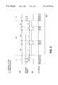
- FIG. 1is a schematic illustration of a fault condition protection device of the invention.
- FIG. 2is a plot illustrating the operation of the device of FIG. 1 .
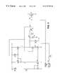
- FIG. 3is a schematic illustration of a second embodiment of the fault condition protection device.
- FIG. 4is a plot illustrating the operation of the device of FIG. 2 .
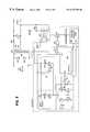
- FIG. 5is a schematic illustration of a switched mode power supply in accordance with the present invention.
- the circuit 200has a primary oscillator 111 which is connected to a counter 202 .
- the counter 202can be reset by a feedback signal which clears registers Q 8 -Q 13 of counter 202 .
- the feedback signalis explained in more detail below.
- An inverter 204receives the 13-th bit output of counter 202 .
- the output of inverter 204is provided to an AND-gate 206 whose other input is connected to a switching signal.
- the switching signalis derived from the oscillator 111 output and the feedback signal. This switching signal cycles periodically when the power supply operates normally. The switching signal is idled when the power supply encounters a fault condition.
- the output of AND-gate 206in turn is provided to the gate of a switching transistor 208 .
- Counter 202eventually causes an AND-gate 206 to shut-off switching transistor 208 and to perform auto-restart.
- a current source 122generates a current I from a supply voltage 120 .
- the output of current source 122is connected to the source of a p-channel MOSFET transistor 125 , whose drain is connected to a node 123 .
- a second current source 184Also connected to the node 123 through a p-channel MOSFET 182 is a second current source 184 .
- Current source 184can supply current which is 1 ⁇ 4 of the current I.
- the drain of transistor 182is also connected to node 123 .
- the gate of transistor 182is driven by an inverter 180 , whose input is connected to the gate of transistor 125 and to the counter output Q 13 .
- the node 123is connected to the sources of p-channel MOSFET transistors 126 and 132 .
- the drain of MOSFET transistor 126is connected to the drain of an n-channel MOSFET transistor 128 .
- the source of transistor 128is grounded, while the gate of transistor 128 is connected to its drain.
- the gate of transistor 128is also connected to the gate of an n-channel MOSFET transistor 130 .
- the source of transistor 130is grounded, while the drain of transistor 130 is connected to the drain of transistor 132 at a node 131 .
- Transistors 126 , 128 , 130 and 132form a differential switch.
- the input of inverter 124 and the gate of transistor 132are driven by a hysteresis comparator 136 .
- Output of inverter 124drives the gate of MOSFET transistor 126 .
- Comparator 136has an input which is connected to node 131 and to a capacitor 134 . The other node of the capacitor is connected to ground.
- transistors 126 , 128 , 130 and 132 , capacitor 134 , inverter 124 and hysteresis comparator 136 and current source 122form an oscillator.
- the output of hysteresis comparator 136is provided as an oscillator output and is also used to drive the clock input of counter 202 .
- the feedback signalperiodically pulses between a low state and a high state depending on the amount of power required on a secondary winding 922 (FIG. 5 ). Every time the feedback signal is low, the feedback signal resets a counter whose states are reflected by outputs Q 8 -Q 13 of counter 202 . The resetting of the counter associated with outputs Q 8 -Q 13 thus occurs regularly when no fault is present in the power supply. The cycling of the feedback signal constantly clears the output bit Q 13 such that the power transistor 208 is controlled by the switching signal when no fault is present. However, in the event of a fault condition, the feedback signal remains high for a sufficiently long time such that the counter associated with output bits Q 8 -Q 13 has enough time to increment output bit Q 13 .
- the setting of the output bit Q 13causes inverter 204 output to go low and thus causes the output of AND-gate 206 to be deasserted.
- the deassertion of AND-gate 206in turn disables switching transistor 208 .
- transistor 125turns off to isolate primary current source 122 from node 123 .
- Thisturns on the transistor 182 via inverter 180 , thus allowing the 1 ⁇ 4 I current to flow from the secondary current source 184 to node 123 .
- the state change of the counter output Q 13causes the oscillator to switch at one-fourth of its normal frequency to achieve about 20% on time and 80% off time. This operation reduces the power delivered by the power supply under a fault condition as well as avoids the possibility of damage to the regulator device and other power supply components such as the output diode or the transformer (not shown).
- FIG. 2shows a timing diagram for the device of FIG. 1 .
- the timing diagram of FIG. 2shows three periods: 211 , 213 and 215 .
- Period 211is normal operation with the feedback signal going “low” more often than a predetermined count such as approximately 4096 clock cycles, thereby resetting the Auto Restart Counter before it counts up to 4096.
- the-feedback signalhas been “high” for 4096 continuous clock cycles due to a fault condition such as an output overload or short, so the circuit of FIG. 1 goes into the auto-restart mode.
- the oscillator frequencyis divided by four and switching transistor 208 has been inhibited from switching, remaining in its off state. After 4096 clock cycles, switching transistor 208 is activated and the oscillator frequency switches back to normal frequency. This sequence will repeat itself as long as the feedback signal stays “high.”
- FIG. 3shows an analog auto restart circuit.
- a current source 525produces a fixed magnitude current 530 .
- Fixed magnitude current 530is fed into first transistor 535 and mirrored to transistors 540 and 545 .
- Third transistor 545is connected to a capacitor 550 via transistor 595 .
- Transistor 600is also connected to the capacitor 550 .
- Transistor 600is controlled by the feedback signal provided to inverter 605 whose output drives the gate of the transistor 600 .
- Node 400is generated by the charging and discharging of capacitor 550 .
- Capacitor 550has a relatively low capacitance which allows for integration on a monolithic chip in one embodiment of the IC regulator of the invention.
- Node 400is provided to a hysteresis comparator 560 which compares its input with a lower limit of about 1.5 volts and an upper limit of about 4.5 volts.
- the output of comparator 560is provided to the gates of transistors 585 and 595 .
- AND-gate 570receives at one input the output of comparator 560 .
- AND-gate 570enables switching transistor 572 to turn on and off.
- AND-gate 570receives at a second input a switching signal which modulates the regulator output.
- capacitor 550In operation, after the feedback signal goes high, capacitor 550 begins to charge from a level below 1.5 volts to an upper threshold of about 4.5 volts. Upon reaching 4.5 volts, the output of comparator 560 switches and discharges the capacitor 550 through transistors 545 and 595 . Node 400 then switches between the upper threshold of about 4.5 volts and the lower threshold of about 1.5 volts.
- Signal 401 output of comparator 560will be high until node 400 exceeds the upper threshold limit.
- signal 400is high, p-channel transistors 585 and 595 are turned off. By turning off transistors 585 and 595 , current can flow into and steadily charge capacitor 550 and increase the magnitude of node 400 .
- the current that flows into capacitor 550is derived from current source 525 because the current through transistor 590 is mirrored from transistor 580 , which current is derived from transistor 540 .
- period 700feedback signal 402 is switching and the system is in normal operation with switching transistor 572 controlled by the switching signal.
- a fault conditionhas been detected and the feedback signal stays high for an extended period of time (period 701 ).
- transistor 700turns off, allowing capacitor 550 to be charged by current source 590 .
- the output 401 of comparator 560goes low, disabling the switching transistor 572 .
- Capacitor 550will be discharged to the first threshold by current source 545 with switching transistor 572 disabled. This mode of oscillation continues until the feedback signal goes low again, indicating that the fault condition no longer exists.
- Direct current (DC) input voltageis provided to a Zener diode 912 which is connected to a diode 914 .
- the diodes 912 - 914 togetherare connected in series across a primary winding of a transformer 920 .
- a secondary winding 922is magnetically coupled to the primary winding of transformer 920 .
- One terminal of the secondary winding 922is connected to a diode 930 , whose output is provided to a capacitor 932 .
- the junction between diode 930 and capacitor 932is the positive terminal of the regulated output.
- the other terminal of capacitor 932is connected to a second terminal of the secondary winding and is the negative terminal of the regulated output.
- a Zener diode 934is connected to the positive terminal of the regulated output.
- the other end of Zener diode 934is connected to a first end of a light emitting diode in an opto-isolator 944 .
- a second end of the light-emitting diodeis connected to the negative terminal of the regulated output.
- a resistor 936is connected between the negative terminal of the regulated output and the first end of the light-emitting diode of opto-isolator 944 .
- the collector of the opto-isolator 944is connected to current source 172 .
- the output of current source 172is provided to the switching regulator logic 800 .
- Power transistor 208Connected to the second primary winding terminal is the power transistor 208 .
- Power transistor 208is driven by AND gate 206 which is connected to inverter 204 and switching regulator logic 800 .
- Switching regulator logic 800receives a clock signal 101 from an oscillator 111 .
- a counter 202also receives the clock signal 101 from the primary oscillator 111 .
- the output of counter 202 , Q 13is used to switch in the current source 184 to supply current in lieu of the current source 122 when Q 13 is high.
Landscapes
- Engineering & Computer Science (AREA)
- Power Engineering (AREA)
- General Engineering & Computer Science (AREA)
- Mechanical Engineering (AREA)
- Dc-Dc Converters (AREA)
Abstract
Description
Claims (41)
Priority Applications (9)
| Application Number | Priority Date | Filing Date | Title |
|---|---|---|---|
| US09/192,871US6337788B1 (en) | 1998-11-16 | 1998-11-16 | Fault condition protection |
| US09/941,905US6456475B1 (en) | 1998-11-16 | 2001-08-29 | Off-line converter with digital control |
| US10/183,927US6687101B2 (en) | 1998-11-16 | 2002-06-25 | Fault condition protection |
| US10/703,702US7099128B2 (en) | 1998-11-16 | 2003-11-07 | Fault condition protection |
| US11/485,548US7446988B2 (en) | 1998-11-16 | 2006-07-11 | Fault condition protection |
| US12/179,438US7773350B2 (en) | 1998-11-16 | 2008-07-24 | Fault condition protection |
| US12/836,518US7881027B2 (en) | 1998-11-16 | 2010-07-14 | Fault condition protection |
| US12/982,652US8184413B2 (en) | 1998-11-16 | 2010-12-30 | Fault condition protection |
| US13/451,383US8542468B2 (en) | 1998-11-16 | 2012-04-19 | Fault condition protection |
Applications Claiming Priority (1)
| Application Number | Priority Date | Filing Date | Title |
|---|---|---|---|
| US09/192,871US6337788B1 (en) | 1998-11-16 | 1998-11-16 | Fault condition protection |
Related Child Applications (2)
| Application Number | Title | Priority Date | Filing Date |
|---|---|---|---|
| US09/941,905ContinuationUS6456475B1 (en) | 1998-11-16 | 2001-08-29 | Off-line converter with digital control |
| US09/941,906ContinuationUS6477835B1 (en) | 2001-08-29 | 2001-08-29 | Single-motor injection-and-screw drive hybrid actuator |
Publications (1)
| Publication Number | Publication Date |
|---|---|
| US6337788B1true US6337788B1 (en) | 2002-01-08 |
Family
ID=22711367
Family Applications (9)
| Application Number | Title | Priority Date | Filing Date |
|---|---|---|---|
| US09/192,871Expired - LifetimeUS6337788B1 (en) | 1998-11-16 | 1998-11-16 | Fault condition protection |
| US09/941,905Expired - LifetimeUS6456475B1 (en) | 1998-11-16 | 2001-08-29 | Off-line converter with digital control |
| US10/183,927Expired - Fee RelatedUS6687101B2 (en) | 1998-11-16 | 2002-06-25 | Fault condition protection |
| US10/703,702Expired - LifetimeUS7099128B2 (en) | 1998-11-16 | 2003-11-07 | Fault condition protection |
| US11/485,548Expired - Fee RelatedUS7446988B2 (en) | 1998-11-16 | 2006-07-11 | Fault condition protection |
| US12/179,438Expired - Fee RelatedUS7773350B2 (en) | 1998-11-16 | 2008-07-24 | Fault condition protection |
| US12/836,518Expired - Fee RelatedUS7881027B2 (en) | 1998-11-16 | 2010-07-14 | Fault condition protection |
| US12/982,652Expired - Fee RelatedUS8184413B2 (en) | 1998-11-16 | 2010-12-30 | Fault condition protection |
| US13/451,383Expired - Fee RelatedUS8542468B2 (en) | 1998-11-16 | 2012-04-19 | Fault condition protection |
Family Applications After (8)
| Application Number | Title | Priority Date | Filing Date |
|---|---|---|---|
| US09/941,905Expired - LifetimeUS6456475B1 (en) | 1998-11-16 | 2001-08-29 | Off-line converter with digital control |
| US10/183,927Expired - Fee RelatedUS6687101B2 (en) | 1998-11-16 | 2002-06-25 | Fault condition protection |
| US10/703,702Expired - LifetimeUS7099128B2 (en) | 1998-11-16 | 2003-11-07 | Fault condition protection |
| US11/485,548Expired - Fee RelatedUS7446988B2 (en) | 1998-11-16 | 2006-07-11 | Fault condition protection |
| US12/179,438Expired - Fee RelatedUS7773350B2 (en) | 1998-11-16 | 2008-07-24 | Fault condition protection |
| US12/836,518Expired - Fee RelatedUS7881027B2 (en) | 1998-11-16 | 2010-07-14 | Fault condition protection |
| US12/982,652Expired - Fee RelatedUS8184413B2 (en) | 1998-11-16 | 2010-12-30 | Fault condition protection |
| US13/451,383Expired - Fee RelatedUS8542468B2 (en) | 1998-11-16 | 2012-04-19 | Fault condition protection |
Country Status (1)
| Country | Link |
|---|---|
| US (9) | US6337788B1 (en) |
Cited By (15)
| Publication number | Priority date | Publication date | Assignee | Title |
|---|---|---|---|---|
| US6480043B2 (en)* | 1999-05-24 | 2002-11-12 | Semiconductor Components Industries Llc | Circuit and method for protecting a switching power supply from a fault condition |
| US20030112573A1 (en)* | 2001-12-13 | 2003-06-19 | Daniel Perez | Method and apparatus for preventing overload in a circuit |
| US20030132738A1 (en)* | 2002-01-17 | 2003-07-17 | Balu Balakrishnan | Method and apparatus for maintaining an approximate constant current output characteristic in a switched mode power supply |
| US20050237041A1 (en)* | 2004-04-26 | 2005-10-27 | Weng Da F | Quasi average current mode control scheme for switching power converter |
| US20070070663A1 (en)* | 2004-03-18 | 2007-03-29 | Stmicroelectronics S.R.L. | Method and related circuit for protection against malfunctioning of the feedback loop in switching power supplies |
| US20080084713A1 (en)* | 2006-10-04 | 2008-04-10 | Stefan Baurle | Method and apparatus for a control circuit with multiple operating modes |
| US20080084198A1 (en)* | 2006-10-04 | 2008-04-10 | Stefan Baurle | Method and apparatus for a power supply controller responsive to a feedforward signal |
| US20080084712A1 (en)* | 2006-10-04 | 2008-04-10 | Zhao-Jun Wang | Method and apparatus for a control circuit responsive to an impedance coupled to a control circuit terminal |
| US20110046807A1 (en)* | 2008-12-31 | 2011-02-24 | Guangdong Electric Power Design Institute | Dcs control module for a transformer in nuclear power engineering |
| US20170033783A1 (en)* | 2015-07-31 | 2017-02-02 | Texas Instruments Incorporated | Method of achieving robustness of the device in short circuit condition by adjusting the current limit threshold based repetitive fault condition |
| US10298109B2 (en)* | 2017-05-03 | 2019-05-21 | Stmicroelectronics (Rousset) Sas | Switch-mode power supply control |
| US10355583B1 (en) | 2018-05-21 | 2019-07-16 | Power Integrations, Inc. | Power converter fault detection by counting request pulses |
| US10404263B2 (en) | 2017-05-03 | 2019-09-03 | Stmicroelectronics (Rousset) Sas | Digital-to-analog converter |
| US11996795B2 (en) | 2022-03-28 | 2024-05-28 | Power Integrations, Inc. | Motor alignment control |
| US12021439B2 (en) | 2019-05-24 | 2024-06-25 | Power Integrations, Inc. | Switching delay for communication |
Families Citing this family (21)
| Publication number | Priority date | Publication date | Assignee | Title |
|---|---|---|---|---|
| US6337788B1 (en)* | 1998-11-16 | 2002-01-08 | Power Integrations, Inc. | Fault condition protection |
| US7656096B2 (en)* | 2003-04-30 | 2010-02-02 | International Rectifier Corporation | Hybrid ballast control circuit in a simplified package |
| US7539028B2 (en)* | 2005-07-01 | 2009-05-26 | Power Integrations, Inc. | Method and apparatus for fault detection in a switching power supply |
| US7245510B2 (en) | 2005-07-07 | 2007-07-17 | Power Integrations, Inc. | Method and apparatus for conditional response to a fault condition in a switching power supply |
| CN100445073C (en)* | 2006-08-02 | 2008-12-24 | 浙江大学 | Injection molding machine manipulator can close the mold signal contact adhesion detection and alarm device |
| CA2567462A1 (en)* | 2006-11-08 | 2008-05-08 | Ivan Meszlenyi | Spike converter |
| US8077486B2 (en)* | 2007-04-06 | 2011-12-13 | Power Integrations, Inc. | Method and apparatus for power converter fault condition detection |
| US8077483B2 (en) | 2007-04-06 | 2011-12-13 | Power Integrations, Inc. | Method and apparatus for sensing multiple voltage values from a single terminal of a power converter controller |
| US10153121B2 (en)* | 2007-11-30 | 2018-12-11 | Hubbell Incorporated | GFCI with miswire protection having unitary receptacle and load conductors after proper installation |
| US8054603B2 (en)* | 2008-10-08 | 2011-11-08 | Himax Analogic, Inc. | Power converter, short detection circuit thereof, and method for detecting short |
| CN101599701B (en)* | 2009-07-02 | 2011-09-28 | 成都芯源系统有限公司 | Switching power supply with fault protection function and control method thereof |
| US8680884B2 (en)* | 2010-03-25 | 2014-03-25 | Cree, Inc. | Fault detection circuits for switched mode power supplies and related methods of operation |
| CN102457049B (en)* | 2010-10-29 | 2014-07-02 | 登丰微电子股份有限公司 | Power conversion controller and LED drive circuit |
| US8988903B2 (en) | 2012-06-11 | 2015-03-24 | Schweitzer Engineering Laboratories, Inc. | Systems and methods for protecting a switch mode power supply |
| JP5935535B2 (en)* | 2012-06-20 | 2016-06-15 | 富士電機株式会社 | Abnormal voltage detector |
| US20160204711A1 (en)* | 2015-01-12 | 2016-07-14 | Xentris Wireless Llc | Power adapter with automatic retry limiter and method of operation |
| US11031804B2 (en)* | 2017-11-06 | 2021-06-08 | Nxp B.V. | Power controller |
| EP3627162B1 (en)* | 2018-09-21 | 2023-06-07 | Maschinenfabrik Reinhausen GmbH | Analyzing an operation of a power semiconductor device |
| US11079443B2 (en)* | 2018-12-21 | 2021-08-03 | Analog Devices International Unlimited Company | Switch fault detection techniques for DC-DC converters |
| EP4186733B1 (en) | 2021-11-24 | 2025-01-01 | Power Integrations, Inc. | Active discharge of an electric drive system |
| US11762447B2 (en) | 2021-12-22 | 2023-09-19 | Schweitzer Engineering Laboratories, Inc. | Power supply with boost stage to improve ride through performance |
Citations (7)
| Publication number | Priority date | Publication date | Assignee | Title |
|---|---|---|---|---|
| US4394703A (en)* | 1981-12-24 | 1983-07-19 | Gte Automatic Electric Labs Inc. | Load protecting arrangement |
| US4761702A (en)* | 1986-04-22 | 1988-08-02 | Mitel Corporation | CMOS latch-up recovery circuit |
| US4887199A (en)* | 1986-02-07 | 1989-12-12 | Astec International Limited | Start circuit for generation of pulse width modulated switching pulses for switch mode power supplies |
| US5550437A (en)* | 1995-04-06 | 1996-08-27 | France/Scott Fetzer Company | Electronic dimmable gas tube power supply with overvoltage protection |
| US5796596A (en)* | 1996-11-15 | 1998-08-18 | Thomson Consumer Electronics, Inc. | Fault control circuit for switched power supply |
| US5874841A (en)* | 1997-07-28 | 1999-02-23 | Philips Electronics North America Corporation | Sample-and-hold circuit for a switched-mode power supply |
| US5949154A (en)* | 1996-11-15 | 1999-09-07 | Thomson Consumer Electronics, Inc. | Auxiliary power supply control |
Family Cites Families (18)
| Publication number | Priority date | Publication date | Assignee | Title |
|---|---|---|---|---|
| US3721836A (en)* | 1971-11-24 | 1973-03-20 | W Rippel | Current limited transistor switch |
| US3733519A (en)* | 1972-04-24 | 1973-05-15 | Motorola Inc | Protection circuit for regulated power supplies |
| US4685020A (en)* | 1985-05-06 | 1987-08-04 | International Business Machines Corp. | Shutdown circuit for blocking oscillator power supply |
| US4823070A (en)* | 1986-11-18 | 1989-04-18 | Linear Technology Corporation | Switching voltage regulator circuit |
| US4825144A (en)* | 1987-11-10 | 1989-04-25 | Motorola, Inc. | Dual channel current mode switching regulator |
| US4812943A (en)* | 1987-12-24 | 1989-03-14 | Sundstrand Corp. | Current fault protection system |
| JPH01303081A (en)* | 1988-05-31 | 1989-12-06 | Nikon Corp | Controller |
| US5029269A (en)* | 1990-04-12 | 1991-07-02 | Rockwell International Corporation | Delayed power supply overvoltage shutdown apparatus |
| US5014178A (en)* | 1990-05-14 | 1991-05-07 | Power Integrations, Inc. | Self powering technique for integrated switched mode power supply |
| US5335162A (en)* | 1993-01-15 | 1994-08-02 | Toko America, Inc. | Primary side controller for regulated power converters |
| JP2784136B2 (en)* | 1993-10-19 | 1998-08-06 | 浜松ホトニクス株式会社 | Switching power supply overload and short circuit protection circuit |
| KR0142467B1 (en)* | 1995-05-26 | 1998-10-01 | 김광호 | Feed back circuit with delayed protection function |
| JPH09140126A (en)* | 1995-05-30 | 1997-05-27 | Linear Technol Corp | Adaptive switch circuit, adaptive output circuit, control circuit, and method for operating switching voltage regulator |
| US5973416A (en)* | 1995-07-20 | 1999-10-26 | Temic Telefunken Microelectronic Gmbh | Method for controlling a power supply switch and circuit arrangement for performing the control |
| US5973419A (en)* | 1997-09-23 | 1999-10-26 | International Business Machines Corporation | Circuit and method of operation to control in-rush current and maintain power supply voltage to peripheral devices in an information system |
| US5862045A (en)* | 1998-04-16 | 1999-01-19 | Motorola, Inc. | Switched mode power supply controller and method |
| US6337788B1 (en)* | 1998-11-16 | 2002-01-08 | Power Integrations, Inc. | Fault condition protection |
| US6480043B2 (en)* | 1999-05-24 | 2002-11-12 | Semiconductor Components Industries Llc | Circuit and method for protecting a switching power supply from a fault condition |
- 1998
- 1998-11-16USUS09/192,871patent/US6337788B1/ennot_activeExpired - Lifetime
- 2001
- 2001-08-29USUS09/941,905patent/US6456475B1/ennot_activeExpired - Lifetime
- 2002
- 2002-06-25USUS10/183,927patent/US6687101B2/ennot_activeExpired - Fee Related
- 2003
- 2003-11-07USUS10/703,702patent/US7099128B2/ennot_activeExpired - Lifetime
- 2006
- 2006-07-11USUS11/485,548patent/US7446988B2/ennot_activeExpired - Fee Related
- 2008
- 2008-07-24USUS12/179,438patent/US7773350B2/ennot_activeExpired - Fee Related
- 2010
- 2010-07-14USUS12/836,518patent/US7881027B2/ennot_activeExpired - Fee Related
- 2010-12-30USUS12/982,652patent/US8184413B2/ennot_activeExpired - Fee Related
- 2012
- 2012-04-19USUS13/451,383patent/US8542468B2/ennot_activeExpired - Fee Related
Patent Citations (7)
| Publication number | Priority date | Publication date | Assignee | Title |
|---|---|---|---|---|
| US4394703A (en)* | 1981-12-24 | 1983-07-19 | Gte Automatic Electric Labs Inc. | Load protecting arrangement |
| US4887199A (en)* | 1986-02-07 | 1989-12-12 | Astec International Limited | Start circuit for generation of pulse width modulated switching pulses for switch mode power supplies |
| US4761702A (en)* | 1986-04-22 | 1988-08-02 | Mitel Corporation | CMOS latch-up recovery circuit |
| US5550437A (en)* | 1995-04-06 | 1996-08-27 | France/Scott Fetzer Company | Electronic dimmable gas tube power supply with overvoltage protection |
| US5796596A (en)* | 1996-11-15 | 1998-08-18 | Thomson Consumer Electronics, Inc. | Fault control circuit for switched power supply |
| US5949154A (en)* | 1996-11-15 | 1999-09-07 | Thomson Consumer Electronics, Inc. | Auxiliary power supply control |
| US5874841A (en)* | 1997-07-28 | 1999-02-23 | Philips Electronics North America Corporation | Sample-and-hold circuit for a switched-mode power supply |
Non-Patent Citations (1)
| Title |
|---|
| Ashok Bindra, "Power-Conversion Chip Cuts Energy Wastage in Off-Line Switchers," Electronic Design, pp. 46,48, Oct. 1998. |
Cited By (47)
| Publication number | Priority date | Publication date | Assignee | Title |
|---|---|---|---|---|
| US6480043B2 (en)* | 1999-05-24 | 2002-11-12 | Semiconductor Components Industries Llc | Circuit and method for protecting a switching power supply from a fault condition |
| US20030112573A1 (en)* | 2001-12-13 | 2003-06-19 | Daniel Perez | Method and apparatus for preventing overload in a circuit |
| US7301319B2 (en) | 2002-01-17 | 2007-11-27 | Power Integrations, Inc. | Methods and apparatus for maintaining an approximate constant current output characteristic in a switched mode power supply |
| US20030132738A1 (en)* | 2002-01-17 | 2003-07-17 | Balu Balakrishnan | Method and apparatus for maintaining an approximate constant current output characteristic in a switched mode power supply |
| US6833692B2 (en)* | 2002-01-17 | 2004-12-21 | Power Integrations, Inc. | Method and apparatus for maintaining an approximate constant current output characteristic in a switched mode power supply |
| US20050088161A1 (en)* | 2002-01-17 | 2005-04-28 | Balu Balakrishnan | Method and apparatus for maintaining an approximate constant current output characteristic in a switched mode power supply |
| US6967472B2 (en) | 2002-01-17 | 2005-11-22 | Power Integrations, Inc. | Method and apparatus for maintaining an approximate constant current output characteristic in a switched mode power supply |
| US7148671B2 (en) | 2002-01-17 | 2006-12-12 | Power Integrations, Inc. | Method and apparatus for maintaining an approximate constant current output characteristic in a switched mode power supply |
| US20070035285A1 (en)* | 2002-01-17 | 2007-02-15 | Balu Balakrishnan | Methods and apparatus for maintaining an approximate constant current output characteristic in a switched mode power supply |
| US7902804B2 (en)* | 2004-03-18 | 2011-03-08 | Stmicroelectronics S.R.L. | Method and related circuit for protection against malfunctioning of the feedback loop in switching power supplies |
| US20070070663A1 (en)* | 2004-03-18 | 2007-03-29 | Stmicroelectronics S.R.L. | Method and related circuit for protection against malfunctioning of the feedback loop in switching power supplies |
| US20050237041A1 (en)* | 2004-04-26 | 2005-10-27 | Weng Da F | Quasi average current mode control scheme for switching power converter |
| US7250744B2 (en)* | 2004-04-26 | 2007-07-31 | Da Feng Weng | Quasi average current mode control scheme for switching power converter |
| US8279627B2 (en) | 2006-10-04 | 2012-10-02 | Power Integrations, Inc. | Method and apparatus for a control circuit with multiple operating modes |
| US8582327B2 (en) | 2006-10-04 | 2013-11-12 | Power Integrations, Inc. | Method and apparatus for a control circuit responsive to an impedance coupled to a control circuit terminal |
| US7502236B2 (en) | 2006-10-04 | 2009-03-10 | Power Integrations, Inc. | Power supply controller responsive to a feedforward signal |
| US7518885B2 (en) | 2006-10-04 | 2009-04-14 | Power Integrations, Inc. | Method and apparatus for a control circuit with multiple operation modes |
| US20090175058A1 (en)* | 2006-10-04 | 2009-07-09 | Power Integrations, Inc. | Method and apparatus for a power supply controller responsive to a feedforward signal |
| US20090185396A1 (en)* | 2006-10-04 | 2009-07-23 | Power Integrations, Inc. | Method and apparatus for a control circuit with multiple operating modes |
| US7576528B2 (en) | 2006-10-04 | 2009-08-18 | Power Integrations, Inc. | Control circuit responsive to an impedance |
| US20090268362A1 (en)* | 2006-10-04 | 2009-10-29 | Power Integrations, Inc. | Method and apparatus for a control circuit responsive to an impedance coupled to a control circuit terminal |
| US10461647B2 (en) | 2006-10-04 | 2019-10-29 | Power Integrations, Inc. | Method and apparatus for a control circuit with multiple operating modes |
| US20080084198A1 (en)* | 2006-10-04 | 2008-04-10 | Stefan Baurle | Method and apparatus for a power supply controller responsive to a feedforward signal |
| US8767414B2 (en) | 2006-10-04 | 2014-07-01 | Power Integrations, Inc. | Method and apparatus for a control circuit with multiple operating modes |
| US8004864B2 (en) | 2006-10-04 | 2011-08-23 | Power Integrations, Inc. | Method and apparatus for a control circuit responsive to an impedance coupled to a control circuit terminal |
| US8148968B2 (en) | 2006-10-04 | 2012-04-03 | Power Integrations, Inc. | Method and apparatus for a power supply controller responsive to a feedforward signal |
| US10211743B2 (en) | 2006-10-04 | 2019-02-19 | Power Integrations, Inc. | Method and apparatus for a control circuit with multiple operating modes |
| US8243480B2 (en) | 2006-10-04 | 2012-08-14 | Power Integrations, Inc. | Method and apparatus for a control circuit responsive to an impedance coupled to a control circuit terminal |
| US20080084713A1 (en)* | 2006-10-04 | 2008-04-10 | Stefan Baurle | Method and apparatus for a control circuit with multiple operating modes |
| US20080084712A1 (en)* | 2006-10-04 | 2008-04-10 | Zhao-Jun Wang | Method and apparatus for a control circuit responsive to an impedance coupled to a control circuit terminal |
| US8437154B2 (en) | 2006-10-04 | 2013-05-07 | Power Integrations, Inc. | Method and apparatus for varying a duty cycle of a power supply controller responsive to multiple linear functions over a range of values of a feedforward signal |
| US8000114B2 (en) | 2006-10-04 | 2011-08-16 | Power Integrations, Inc. | Method and apparatus for a control circuit with multiple operating modes |
| US9343978B2 (en) | 2006-10-04 | 2016-05-17 | Power Integrations, Inc. | Method and apparatus for a control circuit with multiple operating modes |
| US9812973B2 (en) | 2006-10-04 | 2017-11-07 | Power Integrations, Inc. | Method and apparatus for a control circuit with multiple operating modes |
| US8229601B2 (en)* | 2008-12-31 | 2012-07-24 | Guangdong Electric Power Design Institute | DCS control module for a transformer in nuclear power engineering |
| US20110046807A1 (en)* | 2008-12-31 | 2011-02-24 | Guangdong Electric Power Design Institute | Dcs control module for a transformer in nuclear power engineering |
| US20170033783A1 (en)* | 2015-07-31 | 2017-02-02 | Texas Instruments Incorporated | Method of achieving robustness of the device in short circuit condition by adjusting the current limit threshold based repetitive fault condition |
| US10284191B2 (en)* | 2015-07-31 | 2019-05-07 | Texas Instruments Incorporated | Protective circuit enabling different bias levels responsive to event faults |
| US11218147B2 (en) | 2015-07-31 | 2022-01-04 | Texas Instruments Incorporated | Method of achieving robustness of the device in short circuit condition by adjusting the current limit threshold based repetitive fault condition |
| US10812063B2 (en)* | 2015-07-31 | 2020-10-20 | Texas Instruments Incorporated | State machine controlling power transistor through fault and no fault |
| US10298109B2 (en)* | 2017-05-03 | 2019-05-21 | Stmicroelectronics (Rousset) Sas | Switch-mode power supply control |
| US10404263B2 (en) | 2017-05-03 | 2019-09-03 | Stmicroelectronics (Rousset) Sas | Digital-to-analog converter |
| US10811956B2 (en) | 2018-05-21 | 2020-10-20 | Power Integrations, Inc. | Power converter fault detection by counting request pulses |
| US10355583B1 (en) | 2018-05-21 | 2019-07-16 | Power Integrations, Inc. | Power converter fault detection by counting request pulses |
| US12021439B2 (en) | 2019-05-24 | 2024-06-25 | Power Integrations, Inc. | Switching delay for communication |
| US11996795B2 (en) | 2022-03-28 | 2024-05-28 | Power Integrations, Inc. | Motor alignment control |
| US12341462B2 (en) | 2022-03-28 | 2025-06-24 | Power Integrations, Inc. | Motor alignment control |
Also Published As
| Publication number | Publication date |
|---|---|
| US20120206842A1 (en) | 2012-08-16 |
| US7773350B2 (en) | 2010-08-10 |
| US6687101B2 (en) | 2004-02-03 |
| US8184413B2 (en) | 2012-05-22 |
| US7446988B2 (en) | 2008-11-04 |
| US20080304187A1 (en) | 2008-12-11 |
| US20020030957A1 (en) | 2002-03-14 |
| US20060250743A1 (en) | 2006-11-09 |
| US7881027B2 (en) | 2011-02-01 |
| US20020181179A1 (en) | 2002-12-05 |
| US20040095694A1 (en) | 2004-05-20 |
| US8542468B2 (en) | 2013-09-24 |
| US7099128B2 (en) | 2006-08-29 |
| US6456475B1 (en) | 2002-09-24 |
| US20110188274A1 (en) | 2011-08-04 |
| US20100277838A1 (en) | 2010-11-04 |
Similar Documents
| Publication | Publication Date | Title |
|---|---|---|
| US7446988B2 (en) | Fault condition protection | |
| US7310251B2 (en) | Control circuit having two-level under voltage lockout threshold to improve the protection of power supply | |
| US7859865B2 (en) | Method and apparatus for conditional response to a fault condition in a switching power supply | |
| US7453709B2 (en) | Method and apparatus for increasing the power capability of a power supply | |
| US6147883A (en) | Output feedback and under-voltage detection | |
| KR20020079787A (en) | Switching power supply with storage capacitance and power regulation | |
| US6735095B2 (en) | Switched-mode power supply with a function for detecting a broken feedback loop | |
| JP2004297927A (en) | Overcurrent protection circuit | |
| JP2004080859A (en) | Switching power supply control circuit | |
| KR20080000885A (en) | Switching power supply |
Legal Events
| Date | Code | Title | Description |
|---|---|---|---|
| AS | Assignment | Owner name:POWERS INTEGRATIONS, INC., CALIFORNIA Free format text:ASSIGNMENT OF ASSIGNORS INTEREST;ASSIGNORS:BALAKRISHNAN, BALU;DJENGUERIAN, ALEX;LUND, LEIF;REEL/FRAME:009600/0966 Effective date:19981113 | |
| AS | Assignment | Owner name:POWER INTEGRATIONS, INC., CALIFORNIA Free format text:ASSIGNMENT OF ASSIGNORS INTEREST;ASSIGNORS:BALAKRISHNAN, BALU;DJENGUERIAN, ALEX B.;LUND, LEIF;REEL/FRAME:010928/0436 Effective date:19981113 | |
| STCF | Information on status: patent grant | Free format text:PATENTED CASE | |
| FEPP | Fee payment procedure | Free format text:PAYOR NUMBER ASSIGNED (ORIGINAL EVENT CODE: ASPN); ENTITY STATUS OF PATENT OWNER: LARGE ENTITY | |
| FPAY | Fee payment | Year of fee payment:4 | |
| FPAY | Fee payment | Year of fee payment:8 | |
| FPAY | Fee payment | Year of fee payment:12 | |
| IPR | Aia trial proceeding filed before the patent and appeal board: inter partes review | Free format text:TRIAL NO: IPR2018-01814 Opponent name:SEMICONDUCTOR COMPONENTS INDUSTRIES, LLC D/B/A ON Effective date:20180928 Free format text:TRIAL NO: IPR2018-01815 Opponent name:SEMICONDUCTOR COMPONENTS INDUSTRIES, LLC D/B/A ON Effective date:20180928 |