US6337778B1 - Disk drive employing vector addition of primary phase write clock signals for generating secondary phase write clock signal - Google Patents
Disk drive employing vector addition of primary phase write clock signals for generating secondary phase write clock signalDownload PDFInfo
- Publication number
- US6337778B1 US6337778B1US09/318,477US31847799AUS6337778B1US 6337778 B1US6337778 B1US 6337778B1US 31847799 AUS31847799 AUS 31847799AUS 6337778 B1US6337778 B1US 6337778B1
- Authority
- US
- United States
- Prior art keywords
- write clock
- clock signals
- phase
- signal
- secondary phase
- Prior art date
- Legal status (The legal status is an assumption and is not a legal conclusion. Google has not performed a legal analysis and makes no representation as to the accuracy of the status listed.)
- Expired - Lifetime
Links
- 230000010363phase shiftEffects0.000claimsabstractdescription55
- 238000007792additionMethods0.000claims6
- 239000000872bufferSubstances0.000description24
- 230000007704transitionEffects0.000description24
- 238000010586diagramMethods0.000description15
- 230000006870functionEffects0.000description15
- 230000001934delayEffects0.000description12
- 238000012545processingMethods0.000description11
- 238000003860storageMethods0.000description11
- 230000001965increasing effectEffects0.000description9
- 102100031456CentriolinHuman genes0.000description8
- 101000941711Homo sapiens CentriolinProteins0.000description8
- 238000012546transferMethods0.000description8
- 230000002457bidirectional effectEffects0.000description4
- 238000000034methodMethods0.000description4
- 230000036961partial effectEffects0.000description4
- 238000010587phase diagramMethods0.000description4
- 230000005540biological transmissionEffects0.000description3
- 230000008859changeEffects0.000description3
- 230000002860competitive effectEffects0.000description3
- 238000013461designMethods0.000description3
- 230000003993interactionEffects0.000description3
- 230000001360synchronised effectEffects0.000description3
- 238000004891communicationMethods0.000description2
- 238000001514detection methodMethods0.000description2
- 238000000605extractionMethods0.000description2
- 230000005669field effectEffects0.000description2
- 230000001939inductive effectEffects0.000description2
- 238000004519manufacturing processMethods0.000description2
- 230000008569processEffects0.000description2
- 230000002829reductive effectEffects0.000description2
- 230000004044responseEffects0.000description2
- 238000007476Maximum LikelihoodMethods0.000description1
- 230000003044adaptive effectEffects0.000description1
- 230000002411adverseEffects0.000description1
- 239000003990capacitorSubstances0.000description1
- 239000011248coating agentSubstances0.000description1
- 238000000576coating methodMethods0.000description1
- 238000012937correctionMethods0.000description1
- 230000008878couplingEffects0.000description1
- 238000010168coupling processMethods0.000description1
- 238000005859coupling reactionMethods0.000description1
- 238000013500data storageMethods0.000description1
- 230000003247decreasing effectEffects0.000description1
- 230000007547defectEffects0.000description1
- 230000001419dependent effectEffects0.000description1
- 229920005994diacetyl cellulosePolymers0.000description1
- 230000003292diminished effectEffects0.000description1
- 238000007726management methodMethods0.000description1
- 239000000463materialSubstances0.000description1
- 230000010355oscillationEffects0.000description1
- 238000005192partitionMethods0.000description1
- 238000012827research and developmentMethods0.000description1
- 230000011664signalingEffects0.000description1
- 238000009987spinningMethods0.000description1
- 238000012360testing methodMethods0.000description1
- 238000013519translationMethods0.000description1
Images


Classifications
- H—ELECTRICITY
- H03—ELECTRONIC CIRCUITRY
- H03L—AUTOMATIC CONTROL, STARTING, SYNCHRONISATION OR STABILISATION OF GENERATORS OF ELECTRONIC OSCILLATIONS OR PULSES
- H03L7/00—Automatic control of frequency or phase; Synchronisation
- H03L7/06—Automatic control of frequency or phase; Synchronisation using a reference signal applied to a frequency- or phase-locked loop
- H03L7/16—Indirect frequency synthesis, i.e. generating a desired one of a number of predetermined frequencies using a frequency- or phase-locked loop
- H03L7/18—Indirect frequency synthesis, i.e. generating a desired one of a number of predetermined frequencies using a frequency- or phase-locked loop using a frequency divider or counter in the loop
- G—PHYSICS
- G11—INFORMATION STORAGE
- G11B—INFORMATION STORAGE BASED ON RELATIVE MOVEMENT BETWEEN RECORD CARRIER AND TRANSDUCER
- G11B20/00—Signal processing not specific to the method of recording or reproducing; Circuits therefor
- G11B20/10—Digital recording or reproducing
- G11B20/14—Digital recording or reproducing using self-clocking codes
- G11B20/1403—Digital recording or reproducing using self-clocking codes characterised by the use of two levels
- G11B20/1423—Code representation depending on subsequent bits, e.g. delay modulation, double density code, Miller code
- G11B20/1426—Code representation depending on subsequent bits, e.g. delay modulation, double density code, Miller code conversion to or from block codes or representations thereof
- H—ELECTRICITY
- H03—ELECTRONIC CIRCUITRY
- H03L—AUTOMATIC CONTROL, STARTING, SYNCHRONISATION OR STABILISATION OF GENERATORS OF ELECTRONIC OSCILLATIONS OR PULSES
- H03L7/00—Automatic control of frequency or phase; Synchronisation
- H03L7/06—Automatic control of frequency or phase; Synchronisation using a reference signal applied to a frequency- or phase-locked loop
- H03L7/08—Details of the phase-locked loop
- H03L7/099—Details of the phase-locked loop concerning mainly the controlled oscillator of the loop
- H03L7/0995—Details of the phase-locked loop concerning mainly the controlled oscillator of the loop the oscillator comprising a ring oscillator
- G—PHYSICS
- G11—INFORMATION STORAGE
- G11B—INFORMATION STORAGE BASED ON RELATIVE MOVEMENT BETWEEN RECORD CARRIER AND TRANSDUCER
- G11B5/00—Recording by magnetisation or demagnetisation of a record carrier; Reproducing by magnetic means; Record carriers therefor
- G11B5/012—Recording on, or reproducing or erasing from, magnetic disks
Definitions
- the present inventiongenerally relates to generating a write clock signal for writing data in hard disk drives. More particularly, the present invention relates to a disk drive employing vector addition of primary phase write clock signals for generating a secondary phase write clock signal.
- a hard disk drivemust be relatively inexpensive, and must accordingly embody a design that is adapted for low-cost mass production.
- itmust provide substantial capacity, rapid access to data, and reliable performance.
- Numerous manufacturerscompete in this huge market and collectively conduct substantial research and development, at great annual cost, to design and develop innovative hard disk drives to meet increasingly demanding customer requirements.
- Format efficiencyrelates to the percentage of available area that is available for storing user data rather than being consumed by control data, gaps, etc.
- Areal storage densityrelates to the amount of data storage capacity per unit of area on the recording surfaces of the disks.
- the available areal densitymay be determined from the product of the track density measured radially and the linear bit density measured along the tracks.
- the available linear bit densitydepends on numerous factors including the performance capability of certain circuitry that is commonly referred to as a “write channel” and a “read channel.”
- the write channelincludes write precompensation circuitry that provides a write clock signal having a channel frequency corresponding to the rate at which data is to be written on the disk surface (the “data rate”). Increasing the data rate can increase the linear bit density. As the linear bit density increases, nonlinear magnetic transition shifts (non-linear intersymbol interference) may occur due to the magnetic interactions between closely spaced magnetic transitions.
- the read channelincludes sampled data detection circuitry (such as a PRML channel, a EPR4 channel, and a E 2 PR4 channel) that assumes linear intersymbol interference between magnetic transitions recorded on the disk surface during the write operation. Therefore, the write precompensation circuitry in the write channel shifts the phase of the write clock signal in order to shift the time that magnetic transitions are recorded on the disk surface in order to compensate for this nonlinear transition shift problem.
- the phase shift magnitude in the write clock signaldepends on the data pattern that has been and will be recorded on the recording surface.
- a write precompensation circuitthat includes several time delay circuits for generating write clock signals having a phase shift that is selected based on the data pattern.
- the phase shift generated by each time delay circuitis a percentage of the write clock signal.
- the resolution of the phase shiftis determined by the number of delay circuits in the write precompensation circuit (e.g., 5% resolution requires 20 delay circuits). Each delay circuit requires sufficient current for generating the appropriate phase shifts within the clock period.
- finer resolutions of the clock periodare desirable.
- Increasing the number of time delay circuitscan provide finer resolution (e.g., 2% resolution requires 50 delay circuits). However, this can increase the cost of the write precompensation circuit.
- the additional time delay circuitscan result in increased power consumption.
- increased currentis required for each of the time delay circuits in order to timely generate the appropriate phase shifts within the increased clock period. This increased current can also result in increased power consumption.
- U.S. Pat. No. 5,598,364discloses a write precompensation circuit that includes current controlled delay buffers connected to form a delay line having selectable output taps for providing time shift delays.
- the delay of each delay bufferis controllable by a secondary control current derived from a master control current such that the delay is a percentage of an oscillator period.
- the master control currentis also used to control the period of a master write clock generated by a current-controlled ring oscillator of delay buffers.
- a disadvantage with the write precompensation circuit disclosed in the '364 patentis that the magnitude of the resolution for the time delay is limited by the number of delays buffers in the write precompensation circuit.
- U.S. Pat. No. 5,541,961discloses a digital communication system including a phase synthesizer for use in clock extraction circuitry.
- the phase synthesizer disclosed in the '961 patentrequires complex circuitry for weighting and integrating two square wave signals to generate a phase-shifted output signal that is used in the clock extraction circuitry.
- the inventioncan be regarded as a disk drive comprising a disk having a recording surface and write means for writing a sequence of symbols in a continuous-time signal on the recording surface.
- the disk driveincludes a frequency generator for generating a plurality of primary phase write clock signals having a channel frequency f ch , each of the primary phase write lock signals having a selected primary phase shift from another one of the primary phase write clock signals.
- the disk drivefurther includes a programmable phase synthesizer for generating a secondary phase write clock signal having the channel frequency f ch and a selected secondary phase shift from one of the primary phase write clock signals.
- the programmable phase synthesizerincludes programmable means for selecting two of the primary phase write clock signals and means for performing vector addition of the selected primary phase write clock signals to generate the secondary phase write clock signal.
- the disk driveincludes means responsive to the secondary phase write clock signal for providing at least one of the symbols in the sequence of symbols to the write means.
- the inventioncan also be regarded as a disk drive comprising a disk having a recording surface and a write means for writing a sequence of symbols in a continuous-time signal on the recording surface.
- the disk driveincludes a frequency generator for generating a plurality of primary phase write clock signals having a channel frequency f ch , each of the primary phase write clock signals having a selected primary phase shift from another one of the primary phase write clock signals.
- the disk drivefurther includes a plurality of programmable phase synthesizers for generating a plurality of secondary phase write clock signals having the channel frequency f ch and a selected secondary phase shift from one of the primary phase write clock signals.
- Each programmable phase synthesizerincludes programmable means for selecting two of the primary phase write clock signals and means for performing vector addition of the selected primary phase write clock signals to generate one of the plurality of secondary phase write clock signals.
- the disk driveincludes means for selecting a selected one of the secondary phase write clock signals.
- the disk drivefurther includes means responsive to the selected one of the secondary phase write clock signals for providing at least one of the symbols in the sequence of symbols to the write means.
- the inventioncan also be regarded as a disk drive comprising a disk having a recording surface, write means for writing a sequence of symbols in a continuous-time signal on the recording surface, and means for providing a reference frequency signal.
- the disk drivefurther includes first programmable means for providing a channel frequency coefficient and a frequency synthesizer responsive to the reference frequency signal and the channel frequency coefficient for generating a plurality of primary phase write clock signals having a channel frequency f ch .
- the frequency synthesizerincludes a closed loop circuit for tracking the reference frequency signal to generate the plurality of primary phase write clock signals.
- Each of the primary phase write clock signalshas a selected primary phase shift from another one of the primary phase write clock signals.
- the disk drivefurther includes a programmable phase synthesizer for generating a secondary phase write clock signal having the channel frequency f ch and a selected secondary phase shift from one of the primary phase write clock signals.
- the programmable phase synthesizerincludes a second programmable means for selecting two of the primary phase write clock signals, and means for performing vector addition of the selected primary phase write clock signals to generate the secondary phase write clock signal.
- the disk driveincludes means responsive to the secondary phase write clock signal for providing at least one of the symbols in the sequence of symbols to the write means.
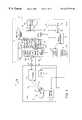
- FIG. 1is a block diagram of a hard disk drive according to an embodiment of the present invention.
- FIG. 2is a partial plan view of a zoned recording surface including a plurality of data tracks having data regions and embedded servo sections.
- FIG. 3is a block diagram of a write channel of the hard disk drive of FIG. 1 .
- FIG. 4Ais a block diagram of a write precompensation circuit in the write channel of FIG. 3 .
- FIG. 4Bis a block diagram of a plurality of programmable phase synthesizers in the write precompensation circuit of FIG. 4 A.
- FIG. 5is a phasor diagram representing six primary phase write clock signals and six secondary phase subsets of secondary phase write clock signals in accordance with an embodiment of the present invention.
- FIG. 6is a diagram of a secondary phase coefficient generator for one of the programmable phase synthesizers of FIG. 4 B.
- FIG. 7is a graphical illustration illustrating absolute step sizes for three secondary phase subsets generated by a linear combination circuit in one of the programmable phase synthesizers of FIG. 4 B.
- FIG. 8is a graphical illustration illustrating relative differences in time step sizes for secondary phase write clock signals for three secondary phase subsets generated by a linear combination circuit in one of the programmable phase synthesizers of FIG. 4 B.
- FIG. 9is a block diagram of a linear combination circuit for one of the programmable phase synthesizers of FIG. 4 B.
- FIG. 10is a schematic diagram of portions of the linear combination circuit of FIG. 9 .
- FIG. 11is a block diagram of a frequency synthesizer for the write channel of FIG. 3 .
- a disk drive 8includes a head disk assembly (HDA) 10 and a printed circuit board assembly (PCBA) 12 .
- HDA 10includes a suitable number of magnetic disks 14 , a spindle motor 16 , a voice coil motor (VCM) 18 , and a preamplifier 22 .
- Spindle motor 16is mechanically coupled to cause disks 14 to rotate at a high spin-rate.
- each disk 14provides two recording surfaces.
- Each of the recording surfaceshas a plurality of data tracks.
- the data tracksare arranged in an embedded servo format having interspersed servo-information regions and user-data regions.
- Each of a suitable number of transducers 20provides for reading from and writing to a respective one of the recording surfaces of disks 14 .
- Suitable types of transducers 20include an inductive transducer and a magnetic resistive (MR) transducer (or a giant magnetic resistive (GMR) transducer).
- Transducers 20can include separate read and write transducers.
- each transducer 20When reading, each transducer 20 generates a low level analog read signal 17 b , which for inductive heads and many MR heads is a differential signal.
- Analog read signal 17 bis conveyed to signal inputs of preamplifier 22 .
- Preamplifier 22produces a read signal 24 which is an amplified, differential, analog read signal.
- HDA 10also includes a path for conveying read signal 24 to PCBA 12 ; a path for conveying a write data signal 28 to preamplifier 22 ; and a path for conveying preamplifier control signals 30 for preamplifier 22 .
- preamplifier 22operates in either a read mode or a write mode and in either case communicates with a selected transducer 20 .
- preamplifier 22provides write current via a write data signal 17 a to a selected transducer 20 for writing a sequence of symbols ⁇ C′ n ⁇ in a continuous-time signal on one of the recording surfaces of disk 14 .
- the write currentchanges polarity upon each change in binary value of write data signal 28 .
- the sequence of symbols ⁇ C′ n ⁇is adversely affected by timing error in the continuous-time signal.
- the timing errorcan result in errors during a read operation.
- An example of timing erroris due to non-linear intersymbol interference between magnetic transitions recorded on the recording surface.
- Read signals 17 b and 24have the same information content, and both are noise-corrupted.
- the servo informationincludes gross-positioning data information including track identification data information, and fine-positioning information in the form of analog servo bursts.
- spindle motor 16is a multi phase, brushless DC motor.
- Well known techniquescan be employed for controlling spindle motor 16 to spin up to, and down from, a substantially constant angular velocity.
- VCM 18is an element of a head-positioning servo system, and applies torque to a head stack assembly (not shown), which includes transducer 20 , to swing the head stack assembly during a track-seeking operation and to maintain it at a desired angular position during a track-following operation.
- PCBA 12includes a channel 26 and a host interface and disk controller (“HIDC 32 ”).
- channel 26 and HIDC 32are each implemented as a single IC, and these two ICs in combination perform overall functions including basic timing functions.
- One such basic timing functionentails the generation of the “global clock” and the synchronization of the global clock to the servo sample rate.
- HIDC 32contains circuitry for generating the global clock which is synchronized to the servo sample rate by a signal supplied by channel 26 .
- HIDC 32contains timing circuitry controlled by the global clock to provide timing signals used in de-multiplexing including separating servo data information from servo bursts and from user data.
- channel 26includes the global clock and timer circuitry.
- channel 26provides, among other things, a signal processing path for processing read signal 24 to produce a clocked, serial-by-symbol data signal (i.e., a decoded binary data signal and accompanying clock signal).
- a signal processing pathfor processing read signal 24 to produce a clocked, serial-by-symbol data signal (i.e., a decoded binary data signal and accompanying clock signal).
- a signal processing paththat processes an analog read signal produced by a preamplifier to produce such a clocked serial-by-symbol data signal is commonly called a “read channel,” such as indicated by read channel 198 .
- Channel 26also provides a signal processing path for processing a clocked serial-by-symbol data signal provided by HIDC 32 to produce a serial-by-bit data signal for the analog signal input of preamplifier 22 .
- a signal processing pathis commonly referred to as a “write channel,” such as indicated by write channel 200 .
- the serial-by-symbol data signalspropagate between channel 26 and HIDC 32 via a channel data bus 38 .
- the clock signals for the serial-by-symbol data signalsare shown collectively as NRZ CLOCKING 41 .
- Channel 26is coupled to receive read signal 24 through a set of coupling capacitors 25 and has a port 40 connected via bus 38 to an NRZ port 45 in HIDC 32 .
- Ports 40 and 45 and interconnecting bus 38propagate data in a clocked, serial-by-symbol form referred to herein as non-return-to-zero (NRZ) form.
- NRZnon-return-to-zero
- the terms “NRZ” and “NRZI” (Non-Return to Zero Inverted) as used hereinhave their customary meaning in this art.
- NRZrefers to a coding system in which a binary 1 is represented (at an instant in time indicated by a clock signal) by a first level or state and a binary 0 is represented (at an instant in time indicated by a clock signal) by a second level or state.
- NRZIrefers to such a clocked coding system in which a binary 1 is represented by a transition from a first level or state to a second level or state and a binary 0 is represented by the absence of a transition.
- channel 26supports use of a partial response, maximum likelihood (PRML) coding system.
- PRMLrefers to a type of signal processing employing sampled and equalized values of an input signal which are evaluated over several samples to estimate symbols contained in the input signal.
- PRMLis one type of a broader class of signal processing systems referred to as “sampled-data processing systems.”
- HIDC 32performs numerous control functions for the disk drive including host interface functions to manage transfer of data between the disk drive and the host, and certain disk controller functions to manage the operation of channel 26 in writing and reading data.
- host interface functionsto manage transfer of data between the disk drive and the host
- certain disk controller functionsto manage the operation of channel 26 in writing and reading data.
- HIDC 32has circuitry for producing certain timing and control signals that are part of a set identified collectively as timing and control signals 44 which are sent between channel 26 and HIDC 32 .
- PCBA 12also includes a data buffer 42 , a microprocessor 34 , a read only memory (ROM) 54 , a writeable random access memory (RAM) 60 , a VCM driver 58 for supplying current to VCM 18 , and a spindle motor driver 56 for supplying current to spindle motor 16 .
- ROM 54is replaced with programmable non-volatile memory, such as flash memory.
- PCBA 12also includes a host interface bus 50 for conveying commands and data between HIDC 32 and the host, a microprocessor bus 36 , a buffer bus 48 for conveying data between HIDC 32 and data buffer 42 , and a path for conveying control signals 30 that provide for bi-directional control interactions between preamplifier 22 and HIDC 32 .
- Microprocessor 34executes instructions acquired from a stored control program to control disk drive functions. These functions include reading and decoding host commands, starting up and controlling the speed of spindle motor 16 , minimizing head-positioning servo off track error through control of VCM 18 , managing reduced power modes of operation, and other disk drive functions. Microprocessor 34 includes an I/O port that is connected to microprocessor bus 36 .
- Microprocessor 34suitably includes an embedded ROM or other non-volatile memory, such as flash memory, that stores some of the control programs it uses.
- control programsinclude the instructions microprocessor 34 executes, and tables, parameters or arguments used during the execution of these programs.
- Microprocessor control programsmay also reside in any or all of ROM 54 , RAM 60 , or data buffer 42 .
- Microprocessor 34 suitablealso includes a register set and a RAM.
- Channel 26has a port 120 and HIDC 32 has a port 35 that connect to microprocessor bus 36 to permit microprocessor 34 to directly communicate with channel 26 and HIDC 32 .
- Microprocessor bus 36also enables microprocessor 34 to communicate directly with ROM 54 and RAM 60 .
- channel data bus 38includes an 8-bit wide (i.e., one byte-wide) parallel path, but can employ more or fewer parallel bits in other embodiments. Depending upon applicable data transfer requirements, a 4-bit wide (nibble-wide) path or even a serial-by-bit path may be suitable for channel data bus 38 .
- write channel 200includes circuitry to accept write data from HIDC 32 via channel data bus 38 and port 40 , to encode write data, and to produce write data signal 28 which is conveyed via preamplifier 22 to a selected transducer 20 .
- write channel 200encodes write data in accordance with Run Length Limited (RLL) code constraints.
- RLLrefers to a type of coding which restricts the minimum and maximum number of binary zeros between binary ones.
- Read channel 198includes circuitry to process read signal 24 , and, on a time-multiplexed basis, generate decoded digital user data, decoded digital servo information data, and a digital representation of demodulated servo burst data.
- the decoded digital servo information data and decoded digital user dataare conveyed to HIDC 32 via port 40 , channel data bus 38 , and HIDC NRZ port 45 .
- Microprocessor 34acquires the demodulated servo burst data via microprocessor port 120 and microprocessor bus 36 , and uses the demodulated servo burst data to perform fine-position head-positioning servo operations.
- An alternative embodimentincorporates servo control circuitry in a servo IC in which case the demodulated servo burst data is provided to such IC.
- HIDC 32includes a buffer port 37 connected to buffer bus 48 , and host interface port 33 connected to host-interface bus 50 .
- HIDC 32includes buffer manager-arbitrator circuitry that manages access to data buffer 42 and manages bidirectional exchange of data between HIDC 32 and data buffer 42 via buffer bus 48 .
- Host interface port 33provides for communicating with the host via host interface bus 50 and host connection 52 .
- host interface port 33includes a set of host interface task file registers.
- Microprocessor 34 and other circuitry within HIDC 32can read task file register contents.
- host interface port 33also includes a set of host command registers and host data registers for parallel transfer of commands and data via host interface bus 50 .
- HIDC 32also controls disk formatting and address translation.
- the translating of addressesincludes translating a logical block address to a cylinder/head/sector address and provides for defect management.
- HIDC 32also includes error detection and correction circuitry that is used to correct errors in user data that were read from disks 14 and stored in data buffer 42 .
- Data buffer 42stores data recovered from a disk 14 , data provided by the host to be recorded on a disk 14 , and, optionally, disk drive commands, servo information data, and control programs for microprocessor 34 .
- the buffer manager within HIDC 32arbitrates access to data buffer 42 when contention for access to data buffer 42 occurs as a consequence of various concurrent operations. Disk drive commands received from the host may be stored in data buffer 42 and be subsequently retrieved by microprocessor 34 .
- ROM 54is an optional conventional ROM IC that stores at least part of the control program used by microprocessor 34 .
- ROM 54may be omitted in an embodiment in which microprocessor 34 includes embedded ROM suitable for replacing the functions of ROM 54 .
- ROM 54is replaced by programmable non-volatile memory, such as flash memory.
- RAM 60is an optional conventional RAM IC used to enlarge the high speed writeable memory available to microprocessor 34 .
- RAM 60is included in PCBA 12 when microprocessor 34 lacks sufficient internal RAM, and data buffer 42 cannot provide microprocessor 34 sufficient external storage or sufficiently fast external storage.
- the hostcan be any electronic system that has an input/output (I/O) bus and interface connection means that is compatible with host connection 52 , host interface bus 50 , and host interface port 33 .
- I/Oinput/output
- FIG. 2is a partial plan view illustrating a recording surface of disk 14 .
- the recording surfaceincludes an inner boundary 150 and an outer boundary 152 .
- Datais stored on concentric, circular data tracks indicated by representative line 154
- Recorded data information (i.e., user data) on the recording surfaceis divided into data regions indicated at 156 .
- Data regions 156can contain data sectors, groups of data sectors or partial data sectors.
- Embedded servo informationis recorded in servo sectors or servo “wedges”, indicated at 158 placed in radially continuous narrow regions between data regions 156 .
- Servo sectors 158include servo information in a number of fields.
- the recording surface of disk 14has five physical recording zones labeled Zone 1 , Zone 2 , Zone 3 , Zone 4 , and Zone 5 which are separated by partitions 160 .
- the recording surface of disk 14may be partitioned into any desirable, usable number of zones, which more typically ranges between 10 to 16 zones.
- the recording zonesare used to assign groups of adjacent data tracks to a plurality of zones between inner boundary 150 and outer boundary 152 .
- the establishment of recording zonespermits efficient recording of data by varying recording frequencies to maintain approximately constant linear bit density across the disk.
- Each recording zoneincludes adjacent data tracks 154 , each of which has data recorded in its data region 156 at a single channel frequency, with the channel frequency varying from recording zone to recording zone.
- the data tracks 154 in each recording zoneincludes servo sectors 158 , each of which has servo information recorded therein at a single channel frequency, with the channel frequency varying from recording zone to recording zone.
- the term “channel frequency” or f ch as used hereinhas its customary meaning in this art. That is, the channel frequency f ch is approximately the reciprocal of a time period “T,” where the “T” is the time period consumed while an elemental-length magnet passes under the transducer during a read operation with the disk spinning at a constant angular velocity.
- the length of each magnet recorded along a track as a result of a write operationis, to a first order of approximation, either an elemental length or an integer multiple of the elemental length.
- channel frequencyis suitably determined by the linear track length, transducer flying height, media quality (e.g., disk surface smoothness, quality of the magnetic coating material, and the like) and constraints imposed by channel 26 .
- media qualitye.g., disk surface smoothness, quality of the magnetic coating material, and the like
- constraints imposed by channel 26e.g., the channel frequency increases in an outward radial direction.
- the channel frequency of the innermost zonehas the smallest channel frequency and the channel frequency increases outwardly from zone to zone, wherein the channel frequency of the outermost zone has the largest channel frequency. This increase in channel frequency from zone to zone (whether for user data or servo data or both) allows linear bit density to be maintained at or near an optimal level while moving from inner to outer data tracks 154 .
- read channel 198provides for processing a read signal that alternately defines servo information data at a servo channel frequency and user data at a data channel frequency different from the servo channel frequency.
- the zone to zone frequency changeneed not be the same from zone to zone, and the number of data tracks within a zone may change from zone to zone. For example, fewer data tracks may be provided in the outer zone than the inner zone.
- Channel 26includes a microprocessor addressable register set 122 ; an address decoder 124 for selecting registers within register set 122 in response to addresses applied to microprocessor port 120 via the bidirectional microprocessor bus 36 , and channel control logic 43 .
- write channel 200receives encoded write data from read channel 198 via a channel write data bus (not shown).
- read channel 198receives write data from HIDC 32 via channel data bus 38 , port 40 , and the internal NRZ data bus, encodes the write data, and forwards the encoded data to write channel 200 .
- Write channel 200performs any required write precompensation according to the present invention, as described in detail below, and generates serial write data signal 28 which is conveyed to preamplifier 22 .
- registers in register set 122contain parameters that control the read and write operations performed by channel 26 .
- Microprocessor 34initializes these registers by writing data into the registers via microprocessor bus 36 , microprocessor port 120 , and register bus 126 .
- Other registers in register set 122are used to store state information generated within read channel 200 .
- microprocessor 34selects a register of register set 122 by sending the address to register address decoder 124 via microprocessor bus 36 , microprocessor port 120 , and an internal register address bus (not shown).
- Address decoder 124decodes the address and generates a register select signal that selects the register to be operated upon.
- Channel 26includes separate bit parallel I/O ports, where port is employed for exchanging NRZ read data and NRZ write data with HIDC 32 and microprocessor port 120 is employed and for providing microprocessor 34 with access to registers in register set 122 .
- Microprocessor 34can directly control channel 26 via microprocessor port 120 and address decoder 124 and can indirectly control channel 26 via control logic in HIDC 32 .
- Use of separate I/O ports for data transfer (via port 40 ) and microprocessor 34 access to register set 122 (via microprocessor port 120 )permits high speed data transfer to occur without interruption via port 40 despite concurrent lower speed data transfers between register set 122 and microprocessor 34 via microprocessor port 120 .
- Microprocessor 34controls channel 26 parameters to optimize channel 26 by employing registers in register set 122 that are writeable by microprocessor 34 .
- microprocessor 34retrieves channel parameters from ROM 54 or other non-volatile memory and initializes channel 26 by storing these parameters in register set 122 . These channel parameters are subsequently used by channel 26 while configuration data are read from reserved data sectors on disks 14 .
- the configuration dataare first stored in data buffer 42 , and subsequently, all or part of this configuration data may be stored in RAM 60 . Subsequent to recovering configuration data from disks 14 , microprocessor 34 uses channel parameters included in the configuration data to initialize register set 122 .
- channel parameter storageincludes any memory in PCBA 12 that provides storage for channel parameter data that microprocessor 34 reads and uses to program the contents of register set 122 and can include embedded ROM or embedded RAM in microprocessor 34 , ROM 54 , RAM 60 , data buffer 42 , or memory in HIDC 32 .
- configuration datarefers to channel parameters recovered from reserved disk tracks and stored in writeable parts of channel parameter storage. Portions of ROM included in microprocessor 34 and/or ROM 54 are used as channel start up parameter storage which stores the channel start up parameters used by channel 26 while configuration data are recovered from the reserved disk drive cylinders.
- Channel parameter storageincludes channel start up parameter storage. Microprocessor 34 recovers channel start up parameters from channel start up parameter storage and loads these parameters into selected registers in register set 122 .
- registers in registers set 122may, for communication with microprocessor 34 , be writeable and readable, readable but not writeable, or writeable but not readable in any suitable combination.
- the circuitry connecting registers in register set 122 to read channel 198 or write channel 200may be from register to channel, channel to register, or bi-directional in a manner suitable for each register.
- microprocessor addressable registers 122are shown grouped separately from read channel 198 and write channel 200 . Preferably, some registers in register set 122 are located near or amongst the read channel 198 or write channel 200 circuitry they serve.
- Port 40receives user write data from and provides user read data and servo read data to HIDC 32 via channel data bus 38 .
- NRZ dataare exchanged between port 40 and read channel 198 in a bidirectional manner via the bidirectional internal NRZ data bus (not shown).
- the Internal NRZ data buspreferably has the same width as channel data bus 38 , for example, eight bits parallel.
- read channel 198provides a NRZ read clock to port 40 , and port 40 sends this clock to HIDC 32 as NRZ clock 41 .
- NRZ clock 41is synchronized with NRZ data being conveyed to HIDC 32 via channel data bus 38 .
- port 40also provides a NRZ write clock to read channel 198 and write channel 200 .
- the NRZ write clockmay be generated by a state machine within port 40 or may optionally be acquired from the NRZ clock 41 as provided by HIDC 32 .
- the data received by read channel 198are encoded by encoder circuitry within read channel 198 and subsequently provided to write channel 200 via the channel write data bus (not shown).
- read channel 198may provide unencoded write data (data as received from port 40 ) to write channel 200 .
- channel control logic 43As for channel control logic 43 , this is shown as being concentrated in a single functional block for convenience of illustration. Some of the circuitry of channel control logic 43 preferably is located near or amongst the other functional blocks included in channel 26 . Some of the signal processing circuitry in channel 26 is pipelined such that certain signals of the set constituting timing and control signals 44 need to be applied to sequential stages of the pipeline with appropriate delays.
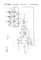
- write channel 200includes a RLL encoder 202 ; a predecoder 204 ; a write precompensation circuit (WPC) 206 ; and a frequency generator, such as a frequency synthesizer 220 .
- Frequency synthesizer 220receives a reference frequency (f ref ) and N and M channel frequency coefficients to generate a plurality of primary phase write clock signals f ch ,f′ ch ,f′′ ch .
- Registers in register set 122 in channel 26provide the N channel frequency coefficient and the M channel frequency coefficient to frequency synthesizer 220 .
- Each of the primary phase write clock signals f ch ,f′ ch ,f′′ chhas a selected primary phase shift, such as 60 degrees, from another one of the primary phase write clock signals f ch ,f′ ch ,f′′ ch .
- the selected primary phase shift between two selected primary phase write clock signals f ch ,f′ ch ,f′′ chdefines a subset of secondary phase write clock signals, such as subsets 350 , 352 , or 354 of FIG. 5 .
- RLL encoder 202receives an input signal from HIDC 32 via channel data bus 38 defining a sequence of input bits ⁇ b n ⁇ , receives primary phase write clock signal f ch , and generates an output signal defining a sequence of code bits ⁇ C n ⁇ .
- RLL encoder 202receives its input signal from channel data bus 38 as a serial by block, parallel by bit signal and provides its output signal as a serial by bit signal to precoder 204 , which is clocked by primary phase write clock signal f CH .
- the RLL encodingrestricts the minimum and maximum number of binary zeros between binary ones and is characterized by parameters (d,k), where d specifies the minimum number of zeros between ones and k specifies the maximum number of zeros between ones.
- Precoder 204receives the sequence of code bits ⁇ C n ⁇ from RLL encoder 202 and generates a sequence of code bits (sequence of symbols) ⁇ C′ n ⁇ which are modified according to a predetermined transfer function. For a channel 26 incorporating PR 4 ML signaling methods, the transfer function commonly used is 1/(1 ⁇ D 2 ) such that the output of precoder 206 equals C′ n ⁇ 2 xor C n . Precoder 204 provides the sequence of symbols ⁇ C′ n ⁇ to write precompensation circuit 206 .
- Write precompensation circuit 206receives the sequence of symbols ⁇ C′ n ⁇ (without write precompensation) and the plurality of primary phase write clock signals f ch ,f′ ch ,f′′ ch to provide the sequence of symbols ⁇ C′ n ⁇ (with write precompensation) on write data signal 28 to a write means, such as preamplifier 22 and transducer 20 .
- a write meanssuch as preamplifier 22 and transducer 20 .
- Each of the primary phase write clock signals (f ch ,f′ ch ,f′′ ch )has a selected primary phase shift (such as 60 degrees) from another one of the primary phase write clock signals (f ch ,f′ ch ,f′′ ch ).
- Preamplifier 22provides write current via write data signal 17 a to transducer 20 for writing the sequence of symbols ⁇ C′ n ⁇ in a continuous-time signal on the recording surface of disk 14 .
- write precompensation circuit 206preferably includes a plurality of programmable phase synthesizers 312 A, 312 B, 312 C and 312 D for generating a plurality of secondary phase write clock signals ⁇ circumflex over ( ⁇ ) ⁇ ch (A), ⁇ circumflex over ( ⁇ ) ⁇ ch (B), ⁇ circumflex over ( ⁇ ) ⁇ ch (C), and ⁇ circumflex over ( ⁇ ) ⁇ ch (D) having the channel frequency f ch .
- Each of the secondary phase write clock signals ⁇ circumflex over ( ⁇ ) ⁇ ch (A), ⁇ circumflex over ( ⁇ ) ⁇ ch (B), ⁇ circumflex over ( ⁇ ) ⁇ ch (C), and ⁇ circumflex over ( ⁇ ) ⁇ ch (D)has a selected secondary phase shift from one of the primary phase write clock signals f ch ,f′ ch ,f′′ ch such that the selected secondary phase shift provides write precompensation for reducing timing error in the continuous-time signal recorded on the recording surface of disk 14 .
- programmable phase synthesizers 312 A, 312 B, 312 C and 312 Dare each programmed to independently generate a selected secondary phase shift.
- one of the secondary phase write clock signals ⁇ circumflex over ( ⁇ ) ⁇ ch (A), ⁇ circumflex over ( ⁇ ) ⁇ ch (B), ⁇ circumflex over ( ⁇ ) ⁇ ch (C), or ⁇ circumflex over ( ⁇ ) ⁇ ch (D)is selected as a secondary phase write clock signal ⁇ circumflex over ( ⁇ ) ⁇ ch for clocking the symbol C′ ch in the sequence of symbols ⁇ C′ n ⁇ to preamplifier 22 on write data signal 28 .
- the secondary phase shift in the selected secondary phase write clock signal ⁇ circumflex over ( ⁇ ) ⁇ chadjusts the time for changing the direction of write current flowing through transducer 20 to adjust the time location of magnetic transitions in the data (symbols) written on the recording surface of disk 14 in order to reduce timing error.
- the secondary phase shift in the selected secondary phase write clock signal ⁇ circumflex over ( ⁇ ) ⁇ chcompensates for expected non-linear time shift due to magnetic interactions between closely spaced magnetic transitions.
- a pattern decoder 302receives the sequence of symbols ⁇ C′ n ⁇ from precoder 204 in a shift register 304 .
- Shift register 304is clocked by the write clock signal f ch received on a differential line from frequency synthesizer 220 .
- differential linesare indicated by thicker lines while single-ended lines are indicated by normal lines. In an alternative embodiment, all single-ended line transmission is utilized instead of differential line transmission.
- Differential line transmissionsuch as illustrated in FIG. 4 A and other following Figures, provides for less noise interference on the data signals transmitted along the differential lines and for simplified generation of synchronized inverted data signals.
- Shift register 304preferably stores the following symbols: the second previously written symbol (C′ n ⁇ 2 ); the previously written symbol (C′ n ⁇ 1 ); the symbol to be written (C′ n ); and the next symbol to be written (C′ n+1 )
- the four symbols C′ n ⁇ 2 , C′ n ⁇ 1 , C′ n , and C′ n ⁇ 1are provided as inputs to a look-up table 306 which provides a two bit delay control signal DLY CNTRL to a delay control adjust circuit 308 that delays the two bit delay control signal DLY CNTRL to multiplexer 314 .
- the symbol to be written (C′ n )is provided from shift register 304 to a data time adjust circuit 310 that delays providing the symbol to be written (C′ n ) to flip flop 316 a and inverter 318 .
- the plurality of phase synthesizers 312 A, 312 B, 312 C, and 312 Dreceive primary phase write clock signals f ch ,f′ ch ,f′′ ch on differential lines from frequency synthesizer 220 and provide secondary phase write clock signals ⁇ circumflex over ( ⁇ ) ⁇ ch (A), ⁇ circumflex over ( ⁇ ) ⁇ ch (B), ⁇ circumflex over ( ⁇ ) ⁇ ch (C), and ⁇ circumflex over ( ⁇ ) ⁇ ch (D) to multiplexer 314 .
- the two bit delay control signal DLY CNTRL from delay control adjust circuitry 308is provided to select inputs of multiplexer 314 to control the selection of one of the secondary phase write clock signals ⁇ circumflex over ( ⁇ ) ⁇ ch (A), ⁇ circumflex over ( ⁇ ) ⁇ ch (B), ⁇ circumflex over ( ⁇ ) ⁇ ch (C), and ⁇ circumflex over ( ⁇ ) ⁇ ch (D) as the selected secondary phase write clock signal ⁇ circumflex over ( ⁇ ) ⁇ ch to be provided as the clock signal to output flip flops 316 a and 316 b .
- the symbol C′ nis provided from data time adjust circuit 310 to a data input of flip flop 316 a and is inverted by an inverter 318 , which provides the inverted symbol C′ n * to a data input of flip flop 316 b.
- Delay control adjust circuitry 308provides a delay adjustment for delaying the two bit delay control select signal DLY CNTRL provided to multiplexer 314 on line 309 in order to compensate for the delay caused by phase synthesizers 312 A- 312 B and align the two bit delay control select signal DLY CNTRL on line 309 with secondary phase write clock signals ⁇ circumflex over ( ⁇ ) ⁇ ch (A), ⁇ circumflex over ( ⁇ ) ⁇ ch (B), ⁇ circumflex over ( ⁇ ) ⁇ ch (C), and ⁇ circumflex over ( ⁇ ) ⁇ ch (D).
- data time adjustment circuitry 310delays symbol C′ n so that C′ n and C′ n * are respectively provided to flip flops 316 a and 316 b to properly align C′ n and C′ n * with the selected secondary phase write clock signal ⁇ circumflex over ( ⁇ ) ⁇ ch .
- the selected secondary phase write clock signal ⁇ circumflex over ( ⁇ ) ⁇ chclocks flip flops 316 a and 316 b at substantially the same time so that the sequence of symbols ⁇ C′ n ⁇ provided on line 28 a and the sequence of symbols ⁇ C′ n * ⁇ provided on line 28 b are properly aligned inverted forms of each other, such that together they form a differential signal as represented on thick line 28 as the write data signal 28 carrying symbols ⁇ C′ n ⁇ to preamplifier 22 .
- Look-up table 306 of pattern decoder 302employs the four symbols C′ n ⁇ 2 , C′ n ⁇ 1 , C′ n , and C′ n+1 to generate the two bit delay control select signal DLY CNTRL for selecting the selected secondary write clock signal ⁇ circumflex over ( ⁇ ) ⁇ ch .
- shift register 304holds more or less symbols than the four symbols held by the shift register 304 illustrated in FIG. 4 A.
- other embodiments of look-up table 306provide more than two bits for the delay control select signal DLY CNTRL for selecting the secondary phase write clock signal ⁇ circumflex over ( ⁇ ) ⁇ ch .
- One suitable implementation of pattern decoder 302where shift register 304 holds four symbols and look-up table 306 provides two bits for delay control select signal DLY CNTRL, is discussed in the following paragraphs.
- Table I belowrepresents one implementation of look-up table 306 for selecting one of the secondary phase write clock signals ⁇ circumflex over ( ⁇ ) ⁇ ch (A), ⁇ circumflex over ( ⁇ ) ⁇ ch (B), ⁇ circumflex over ( ⁇ ) ⁇ ch (C), and ⁇ circumflex over ( ⁇ ) ⁇ ch (D).
- the selected secondary phase shift (delay amount) in each of the secondary phase write clock signals ⁇ circumflex over ( ⁇ ) ⁇ ch (A), ⁇ circumflex over ( ⁇ ) ⁇ ch (B), ⁇ circumflex over ( ⁇ ) ⁇ ch (C), and ⁇ circumflex over ( ⁇ ) ⁇ ch (D)depends on the sequence of symbols ⁇ C′ n ⁇ 2 , C′ n ⁇ 1 , C′ n , C′ n+1 ⁇ in the continuous-time signal that is to be recorded on the recording surface of disk 14 .
- non-linear time shift in the continuous-time signaloccurs primarily as a result of minimum magnetic transition spacings ( 1 T) and occurs with a diminished effect at the next longer magnetic transition spacing ( 2 T).
- the non-linear time shiftapproximately add together.
- the 2 T transition's polarityis opposite to that of the 1 T transition resulting in a non-linear time shift which is approximately the difference between the two non-linear time shifts where they to operate independently.
- look-up table 306selects one of the secondary phase write clock signals ⁇ circumflex over ( ⁇ ) ⁇ ch (A), ⁇ circumflex over ( ⁇ ) ⁇ ch (B), ⁇ circumflex over ( ⁇ ) ⁇ ch (C), and ⁇ circumflex over ( ⁇ ) ⁇ ch (D) as the selected secondary phase write clock signal ⁇ circumflex over ( ⁇ ) ⁇ ch for providing write precompensation to correct for (reduce) these non-linear time shifts by writing the transition shifted by a controlled, pattern dependent amount.
- Secondary phase write clock signal ⁇ circumflex over ( ⁇ ) ⁇ ch (A)has a selected secondary phase shift represented by the delay amount A; secondary phase write clock signal ⁇ circumflex over ( ⁇ ) ⁇ ch (B) has a selected secondary phase shift represented by the delay amount B, where B is less than A; secondary phase write clock signal ⁇ circumflex over ( ⁇ ) ⁇ ch (C) has a selected secondary phase shift represented by the delay amount C, where C is approximately equal to A-B; and secondary phase write clock signal ⁇ circumflex over ( ⁇ ) ⁇ ch (D) has a selected secondary phase shift that is suitably no delay.
- phase synthesizer 312 Dis employed to provide substantially equivalent delay (secondary phase shift) as the other phase synthesizers 312 A, 312 B, 312 C so that secondary phase write clock signal ⁇ circumflex over ( ⁇ ) ⁇ ch (D) is kept in alignment with secondary phase write clock signals ⁇ circumflex over ( ⁇ ) ⁇ ch (A), ⁇ circumflex over ( ⁇ ) ⁇ ch (B), ⁇ circumflex over ( ⁇ ) ⁇ ch (C).
- the selected secondary phase shift (delay amount) in each of the secondary phase write clock signals ⁇ circumflex over ( ⁇ ) ⁇ ch (A), ⁇ circumflex over ( ⁇ ) ⁇ ch (B), ⁇ circumflex over ( ⁇ ) ⁇ ch (C), and ⁇ circumflex over ( ⁇ ) ⁇ ch (D)also depends on the channel frequency f ch .
- each recording zone on the recording surface of disk 14has a predetermined channel frequency f ch , wherein the channel frequency f ch typically increases in an outwardly radial direction, such that the inner most recording zone has the smallest channel frequency f ch , and the outermost recording zone has the largest channel frequency f ch .
- phase delays(secondary phase shifts) A,B,C,D for the above four patterns indicated in Table I.
- an adaptive control systemis used to obtain an optimal (i.e., minimal) bit error rate by selecting appropriate phase delays (secondary phase shifts) corresponding to each of the four patterns of Table I for the channel frequency f ch for writing the sequence of symbols ⁇ C′ n ⁇ in each recording zone on disk 14 .
- These optimized selected phase delays (secondary phase shifts) for each of the four patterns for each of the recording zonesare suitably stored in a reserved disk track as configuration data.
- phase delay selections(secondary phase shifts) corresponding to the patterns indicated in Table I for each corresponding recording zone are recovered from the configuration data as channel parameter data.
- the channel parameter datais read and used by microprocessor 34 to program the contents of a primary phase select register and a secondary phase select register in each of the programmable phase synthesizers 312 A, 312 B, 312 C, and 312 D with appropriate primary and secondary select parameters as discussed in more detail below.
- register set 122 of channel 26includes the primary phase select register and the secondary phase select register in each of the programmable phase synthesizers 312 A, 312 B, 312 C, and 312 D.
- each programmable phase synthesizers 312 A, 312 B, 312 C and 312 Dincludes a circuit, such as linear combination circuits 312 A, 312 B, 312 C, and 312 , that performs vector addition of selected primary phase write clock signals f ch ,f′ ch ,f′′ ch to generate one of the plurality of secondary phase write clock signals ⁇ circumflex over ( ⁇ ) ⁇ ch (A), ⁇ circumflex over ( ⁇ ) ⁇ ch (B), ⁇ circumflex over ( ⁇ ) ⁇ ch (C), and ⁇ circumflex over ( ⁇ ) ⁇ ch (D).
- a circuitsuch as linear combination circuits 312 A, 312 B, 312 C, and 312 , that performs vector addition of selected primary phase write clock signals f ch ,f′ ch ,f′′ ch to generate one of the plurality of secondary phase write clock signals ⁇ circumflex over ( ⁇ ) ⁇ ch (A), ⁇ circumflex over ( ⁇ ) ⁇ ch (B),
- Phase synthesizer 312 Aincludes multiplexer 318 A, primary phase select register 320 A, linear combination circuit 326 A, secondary phase coefficient generator 330 A for generating secondary phase coefficients A 1 and A 2 , and secondary phase select register 328 A.
- Linear combination circuit 326 Aincludes multiplier 332 A, multiplier 336 A, and adder 340 A.
- Phase synthesizer 312 Bincludes multiplexer 318 B, primary phase select register 320 B, linear combination circuit 326 B, secondary phase coefficient generator 330 B for generating secondary phase coefficients B 1 and B 2 , and secondary phase select register 328 B.
- Linear combination circuit 326 Bincludes multiplier 332 B, multiplier 336 B, and adder 340 B.
- Phase synthesizer 312 Cincludes multiplexer 318 C, primary phase select register 320 C, linear combination circuit 326 C, secondary phase coefficient generator 328 C for generating secondary phase coefficients C 1 and C 2 , and secondary phase select register 328 C.
- Linear combination circuit 326 Cincludes multiplier 332 C, multiplier 336 C, and adder 340 C.
- Phase synthesizer 312 Dincludes multiplexer 318 D, primary phase select register 320 D, linear combination circuit 326 D, secondary phase coefficient generator 330 D for generating secondary phase coefficients D 1 and D 2 , and secondary phase select 328 D.
- Linear combination circuit 326 Dincludes multiplier 332 D, multiplier 336 D, and adder 340 D.
- phasor diagram 500illustrates in phase diagram form the plurality of primary phase write clock signals f ch ,f ch ′, and f ch ′′ having the channel frequency f ch , each of the primary phase write clock signals having a selected primary phase shift, such as 60 degrees, from another one of the primary phase write clock signals f ch ,f ch ′, and f ch ′′.
- the phasor representation for each of the primary phase write clock signals f ch ,f ch ′, and f ch ′′represents a sine-wave, where the length of an arrow represents a write clock signal magnitude and the angle represents a write clock signal phase.
- programmable phase synthesizers 312 A, 312 B, 312 C and 312 Dare each responsive to two of the primary phase write clock signals f ch ,f ch ′,f ch ′′, and ⁇ f ch to generate secondary phase write clock signals, such as ⁇ circumflex over ( ⁇ ) ⁇ ch (A), ⁇ circumflex over ( ⁇ ) ⁇ ch (B), ⁇ circumflex over ( ⁇ ) ⁇ ch (C), and ⁇ circumflex over ( ⁇ ) ⁇ ch (D), in subset ranges 350 , 352 , and 354 , which thereby permit 180° (i.e., 50%) phase delays (time shifts) for the selected secondary phase write clock signal ⁇ circumflex over ( ⁇ ) ⁇ ch .
- Programmable phase synthesizers 312 A, 312 B, 312 C and 312 Dare also responsive to selected secondary phase coefficients to obtain the desired resolution (step) for the secondary phase shift for each of the secondary phase write clock signals from a respective one of the primary phase write clock signals f ch ,f ch ′, and f ch .
- the primary phase write clock signal f ch ′is shifted 60° (i.e., 16.7%) from primary phase write clock signal f ch .
- Primary phase write clock signal f ch ′′is shifted 120° (i.e., 33.3%) from primary phase write clock signal f ch .
- Primary phase write clock signal ⁇ f chis shifted 180° (i.e., 50%) from primary phase write clock signal f ch .
- primary phase write clock signals ⁇ f ch ′ and ⁇ f ch ′′are respectively shifted 180° from the primary phase write clock signals f ch ′ and f ch ′′.
- phase diagram of FIG. 5illustrates another range (subsets 350 , 352 , 354 , 356 , 358 , and 360 ) that permits up to 360 degree phase shifts from the primary phase write clock signal f ch .
- the phasor diagram of FIG. 5illustrates a subset of secondary phase write clock signals between each of the primary phase write clock signals f ch , f ch ′, f ch ′′, ⁇ f ch , ⁇ f ch ′ and ⁇ f ch ′′.
- Subset 350 of secondary phase write clock signalshas a range between and includes primary phase write clock signals f ch and f ch ′ (i.e., between 0° and 60° phase or time shift).
- Subset 352 of secondary phase write clock signalshas a range between and includes primary phase write clock signals f ch ′ and f ch ′′ (i.e., between 60° and 120° phase or time shift).
- Subset 354 of secondary phase write clock signalshas a range between and includes primary phase write clock signals f ch ′′ and ⁇ f ch (i.e., between 120° and 180° phase or time shift).
- Subset 356 of secondary phase write clock signalshas a range between and includes primary phase write clock signals ⁇ f ch and ⁇ f ch ′ (i.e., between 180° and 240° phase or time shift).
- Subset 358 of secondary phase write clock signalshas a range between and includes primary phase write clock signals ⁇ f ch ′ and ⁇ f ch ′′ (i.e., between 240° and 300° phase or time shift).
- Subset 360 of secondary phase write clock signals 360has a range between and includes primary phase write clock signals ⁇ f ch ′′ and f ch (i.e., between 300° and 360° phase or time shift).
- phase synthesizer 312 A of FIG. 4BFor clarity, the following discussion only refers to phase synthesizer 312 A of FIG. 4B, but the discussion applies equally to the phase synthesizers 312 B, 312 C, and 312 D.
- multiplexer 318 Asuitably receives differential primary phase write clock signals f ch , f ch ′, f ch ′′, ⁇ f ch , ⁇ f ch ′ and ⁇ f ch ′′.
- Multiplexer 318 Areceives three primary phase select bits from primary phase select register 320 A for selecting two of the differential primary phase write clock signals f ch , f ch ′, f ch ′′, ⁇ f ch , ⁇ f ch ′, or ⁇ f ch ′′ as outputs on differential lines 322 A and 324 A.
- any one of the primary phase write clock signals f ch , f ch ′, f ch ′′, ⁇ f ch , ⁇ f ch ′, or ⁇ f ch ′′can be provided from multiplexer 318 A.
- the primary phase select register 320 Aprovides the three primary phase select bits to control the selection of two primary phase write clock signals to select one of the subsets 350 , 352 , 354 , 356 , 358 , or 360 of secondary phase write clock signals.
- the primary phase select register 320 Ais suitably one of the registers in register set 122 in channel 26 , which are programmed by microprocessor 34 as explained above.
- the selected primary phase write clock signals on lines 322 A and 324 Aare provided to linear combination circuit 326 A.
- Secondary phase select register 328 Aprovides four secondary phase select bits to secondary phase coefficient generator 330 A. In other embodiments of the present invention, secondary phase select register 328 A provides more or less than four bits to secondary phase coefficient generator 330 A. The number of bits provided by secondary phase select register 328 A defines the number of phase shifts that are available in each subset.
- the secondary phase select register 328 Ais suitably one of the registers in register set 122 in channel 26 , which are programmed by microprocessor 34 as explained above.
- Secondary phase coefficient generator 330 Agenerates two secondary phase coefficients A 1 and A 2 that are provided to linear combination circuit 326 A.
- Linear combination circuit 326 Aincludes multiplier 332 A which receives the selected primary phase write clock signal on line 324 A and secondary phase coefficient A 1 from secondary phase coefficient generator 330 A and multiplies these inputs together to provide a first vector signal output on a differential line 334 A. Similarly, the selected primary phase write clock signal on line 322 A and secondary phase coefficient A 2 generated by secondary phase coefficient generator 330 A are received and multiplied by multiplier 336 A which provides a second vector signal output on differential line 338 A.
- Adder 340 Aadds the first vector signal output on differential line 334 A and the second vector signal output on differential line 338 A and provides secondary phase write clock signal ⁇ circumflex over ( ⁇ ) ⁇ ch (A) as a single-ended secondary phase write clock signal to multiplexer 314 .
- phase shift ⁇represents a phase shift from one of the primary phase write clock signals f ch , f ch ′, f ch ′′, ⁇ f ch , ⁇ f ch ′, or ⁇ f ch ′′ in a selected subset ( 350 , 352 , 354 , 356 , 358 , 360 ).
- linear combination circuit 326 Asuitably produces the following first order linear polynomial equation for phase synthesizer 312 A: secondary phase write clock signal ⁇ circumflex over ( ⁇ ) ⁇ ch (A) is equal to A 1 P 1 +A 2 P 2 , where P 1 represents the programmably selected primary phase write clock signal on differential line 324 A and P 2 represents the programmably selected primary phase write clock signal on differential line 322 A.
- linear combination circuit 326 Areceives more than two primary phase write clock signals (P) and/or more than two secondary phase coefficients (A), which are thereby combined in a first order linear polynomial equation.
- linear combination circuit 326 Ais replaced with a second or higher order polynomial combination circuit.
- the A 1 [3:0] secondary coefficient bitsare respectively inverted by inverters 370 a , 370 b , 370 c and 370 d to produce respectively secondary phase coefficient bits A 2 [3:0].
- a look-up tableprovides the two secondary phase coefficient outputs based on a four bit secondary phase select signal from secondary phase select register 328 A according to any desired algorithm for correlating the output state of the secondary phase coefficients to the controlling input state of the secondary phase select signal.
- the theoretical (linear) precompensation delay percentages for each of the sixteen incremental steps in each of the secondary phase subsets 350 , 352 , and 354is plotted in absolute terms in FIG. 7 .
- the final step of secondary phase subset 350is the same absolute percentage as the first step of secondary phase subset 352 .
- the last step of secondary phase subset 352is the same absolute percentage as the first step of secondary phase subset 354 .
- secondary phase subset 350has steps from 0 to 16.7%
- secondary phase subset 352has steps from 16.7% to 33.3%
- secondary phase subset 354has steps from 33.3% to 50%.
- An example overlap situation between subsets 350 and 352results as follows.
- the secondary phase coefficient generator 330 A illustrated in FIG. 6can be used for implementing a suitable algorithm for obtaining the secondary phase coefficients for generating the secondary phase write clock signal ⁇ circumflex over ( ⁇ ) ⁇ ch (A).
- FIG. 9is a block diagram of one embodiment of linear combination circuit 326 A.
- multiplier 336 Aincludes voltage-to-current converter 380 , (+) multiplication DAC 388 a , and ( ⁇ ) multiplication DAC 388 b .
- Multiplier 332 Aincludes voltage-to-current converter 384 , (+) multiplication DAC 390 a , and ( ⁇ ) multiplication DAC 390 b .
- Adder 340 Aincludes adding nodes 392 a and 392 b and op amp comparator 394 .
- Voltage-to-current converter 380receives a first primary phase voltage (V in1 ) on the differential line represented by 322 a and 322 b .
- Voltage-to-current converter 384receives a second primary phase voltage (V in2 ) on the differential line represented by 324 a and 324 b .
- Voltage-to-current converters 380 and 384respectively provide a current representative signal on differential lines ( 382 a and 382 b ) and ( 386 a and 386 b ) which is responsive to the respective V in1 and V in2 primary phase input voltages.
- the (+) current multiplication digital-to-analog converter (DAC) 388receives the current representative signal on line 382 a and multiplies it by secondary phase coefficient A 1 [3:0].
- the ( ⁇ ) current multiplication DAC 388 breceives the current representative signal on line 382 b and multiplies it by secondary phase coefficients A 1 [3:0].
- the(+) multiplication DAC 390 areceives the current representative signal 386 a and multiplies it by the secondary phase coefficients A 2 [3:0]
- the ( ⁇ ) multiplication DAC 390 breceives the current representative signal 386 b and multiplies it by secondary phase coefficients A 2 [3:0].
- (+) multiplication DAC 388 aprovides a product result current signal on line 338 a
- ( ⁇ ) multiplication DAC 388 dprovides a product result current signal on line 338 b
- (+) multiplication DAC 390 aprovides a product result current signal on line 334 a
- ( ⁇ ) multiplication DAC 390 bprovides a product result current signal on line 334 b.
- the currents from lines 338 a and 334 aare added together at node 392 a .
- the currents of lines 338 b and 334 bare added together at node 392 b .
- the current signals at nodes 392 a and 392 btogether form a differential signal which is provided to a comparator 394 which compares the two current signals and provides a single-ended secondary phase voltage signal (V out ).
- Voltage-to-current converter 380(which is also representative of voltage-to-current converter 384 ) and (+) multiplication DAC 388 a (which is also representative of multiplication DACs 388 b , 390 a , and 390 b ) are illustrated in detailed schematic diagram form in FIG. 10 .
- Voltage-to-current converter 380includes N-channel field effect transistors (N-FETs) 402 a and 402 b , which respectively receive the primary phase voltage ⁇ V in1 on lines 322 a and 322 b at their gates.
- N-FETsN-channel field effect transistors
- Voltage-to-current converter 380also includes P-channel field effect transistors (P-FETs) 404 a and 404 b , which are respectively coupled between a power supply and the drains of N-FETs 402 a and 402 b .
- P-FETsP-channel field effect transistors
- N-FETs 406 a and 406 bare respectively coupled between the sources of N-FETs 402 a and 402 b and ground.
- a resistor 408is coupled between the sources of transistors 402 a and 402 b .
- N-FETs 406 a and 406 bare provided with a bias voltage (V bias )
- V biasbias voltage
- the drains of P-FETs 404 a and 404 bare respectively coupled to their gates and these junctions respectively provide voltages +V out and ⁇ V out .
- Voltage-to-current converter 380operates such that the voltage ( ⁇ V in1 ) at the input gates of N-FETs 402 a and 402 b respectively controls the amount of current flowing from the power supply to ground through a first current path comprising P-FET 404 a , N-FET 402 a , and N-FET 406 a , and the amount of current flowing from the power supply to ground through a second current path comprising P-FET 404 b , N-FET 402 b , and N-FET 406 b .
- the +V out voltage at the gate of P-FET 404 a and the ⁇ V out voltage at the gate of P-FET 404 bare respectively representative of the current flowing through the first current path and the second current path.
- the +V out voltageis provided on line 382 a to the gates of current source P-FETs 410 , 412 , 414 , and 416 of (+) multiplication DAC 388 a .
- Current source P-FETs 410 , 412 , 414 , and 416have their sources coupled to the power supply and provide currents from their drains which mirror (with a scaling factor) the current flowing from the source-to-drain of P-FET 404 a (i.e., the first current path as defined above for voltage-to-current converter 380 ), because the control gates of current source P-FETs 410 , 412 , 414 , and 416 are coupled to the +V out voltage at the gate and drain junction of P-FET 404 a.
- Current source P-FET 410is sized to provide approximately one unit of current from its drain which mirror the current provided from the drain of P-FET 404 a .
- Current source P-FET 412is double the size of P-FET 410 to provide twice the current or two units of current from its drain.
- Current source P-FET 414is four times the size of P-FET 410 to provide four times the current or four units of current from its drain.
- Current source P-FET 416is eight times the size of P-FET 410 to provide eight times the current or eight units of current from its drain.
- Secondary phase coefficient bits A 1 [3:0]are respectively provided to control the gates of N-FETs 418 a , 418 b , 418 c , and 418 d .
- Secondary phase coefficient bits A 1 [3:0]are respectively inverted by inverters 422 a , 422 b , 422 c , and 422 d to respectively be provided to the control gates of P-FETs 420 a , 420 b , 420 c , and 420 d .
- N-FET 418 a and P-FET 420 aare each coupled between the drain of current source P-FET 410 and output line 338 a .
- N-FET 418 b and P-FET 420 bare each coupled between the drain of current source P-FET 412 and output line 338 a .
- N-FET 418 c and P-FET 420 care each coupled between the drain of current source P-FET 414 and output line 338 a .
- N-FET 418 d and P-FET 420 dare each coupled between the drain of current source P-FET 416 and output line 338 a . In this way, if a secondary phase coefficient A 1 bit is a logic one level, the current from the corresponding current source P-FET is provided to output line 338 a.
- Output line 338 acarries a total output current which is the sum of the currents provided through transistor pairs 418 a & 420 a , 418 b & 420 b , 418 c & 420 c , and 418 d & 420 d .
- secondary phase coefficient A 1 [3]is a logic one level
- eight units of currentare added to output line 338 a .
- secondary phase coefficient A 1 [2]is a logic one level
- four units of currentare added to output line 338 a .
- secondary phase coefficient A 1 [1]is a logic one level
- two units of currentare added to output line 338 a .
- secondary phase coefficient A 1 [0]is a logic one level, then one unit of current is added to output line 338 a.
- Frequency Synthesizer 220is illustrated in block diagram form in FIG. 11.
- a reference frequency clock signalis generated by an oscillator in channel 26 or alternatively in HIDC 32 .
- the reference frequency f refis set to approximately 10 megahertz (MHz).
- the reference frequency f ref from the oscillatoris an analog signal and is provided to frequency synthesizer 220 on a line 502 .
- Registers in register set 122 in channel 26provide an N channel frequency coefficient on a line 503 and an M channel frequency coefficient on a line 504 to frequency synthesizer 220 .
- Frequency synthesizer 220includes frequency divider circuit 506 which receives the N channel frequency coefficient on line 503 and the reference frequency f ref on line 502 and performs frequency division to produce an output signal 507 having a frequency equal to f ref /N.
- Frequency synthesizer 220includes frequency divider circuit 508 which receives the M channel frequency coefficient on line 504 and a representative form of the primary phase write clock signal, such as primary phase write clock signal f ch ′′, from a voltage controlled oscillator (VCO) 522 on a line 510 .
- VCOvoltage controlled oscillator
- the output signals ( 507 and 509 ) from frequency divider circuits 506 and 508are provided to frequency phase detector 512 which detects differences between the output signals. If the channel frequency f ch needs to be sped up to make the inputs to frequency detector more equal, frequency phase detector 512 pulses an output line 514 a to control a charge pump 516 to increase the capacitance voltage in a loop filter 518 . If the channel frequency f ch needs to be slowed down to make the inputs to frequency phase detector 512 more equal, frequency phase detector 512 pulses an output line 514 b to control charge pump 516 to reduce the capacitance voltage in loop filter 518 . The output voltage of loop filter 518 is provided on a line 520 to VCO 522 .
- VCO 522is controlled by the voltage on line 520 and suitably includes three time delay circuits 524 , 526 , and 528 .
- Time delay circuit 524provides primary phase write clock signal f ch .
- Time delay circuit 526provides primary phase write clock signal f ch ′.
- Time delay circuit 528provides primary phase write clock signal f ch ′′.
- the voltage on line 520controls the oscillation period (i.e., frequency) for the channel frequency f ch , but the relative delays between the different primary phase write clock signals f ch , f ch ′, and f ch ′′ provided from time delay circuits 524 , 526 , and 528 remains constant.
- VCO 522provides the primary phase write clock signals f ch , f ch ′, and f ch ′′ and as differential signals.
- a comparator 530compares the primary phase write clock signals from time delay circuit 528 to produce the single-ended primary phase write clock signal f ch ′′ on line 510 , which is provided to frequency divider 508 .
- Each of the time delay circuits 524 , 526 , and 528provide 60° (i.e., 16.7%) phase shifting between the primary phase write clock signals.
- the closed loop circuit formed by frequency phase detector 512 , charge pump 516 , loop filter 518 , VCO 522 , and voltage divider circuits 506 and 508provides closed loop control to force the two inputs from frequency divider 506 and 508 to be equal.
- the closed loop circuittracks the reference frequency signal to generate the primary phase write clock signals f ch , f ch ′, and f ch ′′.
- phase synthesizers in the write precompensation circuit 206can produce fine resolution incremental steps of phase delays of a channel frequency, such as approximately 1% steps.
- the phase shifting used to produce the fine resolution stepsdoes not require excessive power or excessive amounts of circuitry.
Landscapes
- Engineering & Computer Science (AREA)
- Signal Processing (AREA)
- Digital Magnetic Recording (AREA)
- Signal Processing For Digital Recording And Reproducing (AREA)
Abstract
Description
| TABLE I | ||||
| NRZ Representation | ||||
| (ones or zeros represent | ||||
| the two magnetic states | ||||
| Pattern | NRZI Representation | so the present transition | ||
| (spacing from | (ones represent transitions) | is (“between” states) | ||
| previous | Present transition | Present transition ↓ | Function | |
| transition) | ↓ | C′n−2 | C′n−1 | C′n | C′n+1 | (delay by :) |
| 0 | 1 | 1 | 0 | 0 | 1 | 0 | |||
| 1 | 1 | 0 | 1 | ||||||
| 1 | 0 | 1 | 0 | 1 | 1 | 0 | |||
| 1 | 0 | 0 | 1 | (B < A) | |||||
| Both | 1 | 1 | 1 | 0 | 1 | 0 | 1 | ||
| 1 | 0 | 1 | 0 | (approx. A − B) | |||||
| > | 0 | 0 | 1 | 0 | 0 | 0 | 1 | no | |
| 1 | 1 | 1 | 0 | ||||||
| No transition | X | X | 0 | X | 1 | 1 | no | ||
| X | X | ||||||||
| 0 | 0 | ||||||||

Claims (23)
Priority Applications (1)
| Application Number | Priority Date | Filing Date | Title |
|---|---|---|---|
| US09/318,477US6337778B1 (en) | 1999-05-25 | 1999-05-25 | Disk drive employing vector addition of primary phase write clock signals for generating secondary phase write clock signal |
Applications Claiming Priority (1)
| Application Number | Priority Date | Filing Date | Title |
|---|---|---|---|
| US09/318,477US6337778B1 (en) | 1999-05-25 | 1999-05-25 | Disk drive employing vector addition of primary phase write clock signals for generating secondary phase write clock signal |
Publications (1)
| Publication Number | Publication Date |
|---|---|
| US6337778B1true US6337778B1 (en) | 2002-01-08 |
Family
ID=23238346
Family Applications (1)
| Application Number | Title | Priority Date | Filing Date |
|---|---|---|---|
| US09/318,477Expired - LifetimeUS6337778B1 (en) | 1999-05-25 | 1999-05-25 | Disk drive employing vector addition of primary phase write clock signals for generating secondary phase write clock signal |
Country Status (1)
| Country | Link |
|---|---|
| US (1) | US6337778B1 (en) |
Cited By (158)
| Publication number | Priority date | Publication date | Assignee | Title |
|---|---|---|---|---|
| US20030218817A1 (en)* | 2002-05-23 | 2003-11-27 | Texas Instruments, Inc. | Method of controlling reader amplifier gain variations of a HDD preamplifier, or the like |
| US20040003193A1 (en)* | 2002-06-27 | 2004-01-01 | International Business Machines Corporation | Method and apparatus for enhanced phase alignment for direct access storage device (DASD) |
| US6867625B1 (en)* | 2003-09-24 | 2005-03-15 | Itt Manufacturing Enterprises, Inc. | Method and apparatus for high frequency digital carrier synthesis from plural intermediate carrier waveforms |
| US20050190473A1 (en)* | 2004-02-26 | 2005-09-01 | Hitachi Global Technologies Netherlands B.V. | Method and apparatus for providing generalized write pre-compensation |
| US20050190474A1 (en)* | 2004-02-26 | 2005-09-01 | Hitachi Global Technologies Netherlands B.V. | Method and apparatus for providing write pre-compensation using a read timing path |
| US20060072231A1 (en)* | 2004-10-06 | 2006-04-06 | Fischer Jonathan H | Current mirrors having fast turn-on time |
| US20060119965A1 (en)* | 2004-12-03 | 2006-06-08 | Hitachi Global Storage Technologies Netherlands B.V. | Information recording device using patterned medium and control method thereof |
| US20070233945A1 (en)* | 2006-04-04 | 2007-10-04 | Johnson Yen | Systems and methods for accessing read channel registers using commands on data lines |
| US20070272751A1 (en)* | 2006-05-24 | 2007-11-29 | Fujitsu Limited | Storage device having self-diagnosis function, control device that controls self-diagnosis function in storage device, and method of performing self-diagnosis on storage device |
| US7515368B1 (en)* | 2001-05-09 | 2009-04-07 | Marvell International, Ltd. | Precompensation circuit for magnetic recording |
| US20090161245A1 (en)* | 2007-12-21 | 2009-06-25 | Lsi Corporation | Frequency Domain Approach for Efficient Computation of Fixed-point Equalization Targets |
| US20100053793A1 (en)* | 2008-08-27 | 2010-03-04 | Lsi Corporation | Systems and Methods for Adaptive Write Pre-Compensation |
| US20100088357A1 (en)* | 2008-10-08 | 2010-04-08 | Lsi Corporation | Systems and Methods for Memory Efficient Signal and Noise Estimation |
| US20100157768A1 (en)* | 2008-12-18 | 2010-06-24 | Mueller Brian K | Systems and Methods for Generating Equalization Data Using Shift Register Architecture |
| US20100157460A1 (en)* | 2008-12-18 | 2010-06-24 | Lsi Corporation | Systems and Methods for Generating Equalization Data |
| US20100157464A1 (en)* | 2008-12-18 | 2010-06-24 | Lsi Corporation | Systems and Methods for Adaptive MRA Compensation |
| US20100157459A1 (en)* | 2008-12-18 | 2010-06-24 | Lsi Corporation | Systems and Methods for Controlling Data Equalization |
| US20100172046A1 (en)* | 2009-01-02 | 2010-07-08 | Lsi Corporation | Systems and Methods for Equalizer Optimization in a Storage Access Retry |
| US20110018748A1 (en)* | 2009-07-27 | 2011-01-27 | Lsi Corporation | Systems and Methods for Two Tier Sampling Correction in a Data Processing Circuit |
| US20110063747A1 (en)* | 2009-09-14 | 2011-03-17 | Lsi Corporation | Systems and Methods for Timing and Gain Acquisition |
| US7957251B2 (en) | 2009-02-16 | 2011-06-07 | Agere Systems Inc. | Systems and methods for reduced latency loop recovery |
| US7974030B2 (en) | 2008-12-23 | 2011-07-05 | Lsi Corporation | Systems and methods for dibit correction |
| US20110226729A1 (en)* | 2007-11-01 | 2011-09-22 | Western Digital Technologies, Inc. | Method of manufacturing a double sided flex circuit for a disk drive wherein a first side lead provides an etching mask for a second side lead |
| US8175201B2 (en) | 2007-12-21 | 2012-05-08 | Lsi Corporation | Systems and methods for adaptive equalization in recording channels |
| US8762440B2 (en) | 2011-07-11 | 2014-06-24 | Lsi Corporation | Systems and methods for area efficient noise predictive filter calibration |
| US8848776B1 (en) | 2013-03-25 | 2014-09-30 | Lsi Corporation | Systems and methods for multi-dimensional signal equalization |
| US8854752B2 (en) | 2011-05-03 | 2014-10-07 | Lsi Corporation | Systems and methods for track width determination |
| US8879188B1 (en) | 2010-08-23 | 2014-11-04 | Western Digital Technologies, Inc. | Disk drive employing fly height calibration tracks to account for magnetic entropy and thermal decay |
| US8891341B1 (en) | 2013-03-11 | 2014-11-18 | Western Digital Technologies, Inc. | Energy assisted magnetic recording disk drive using modulated laser light |
| US8891193B1 (en) | 2013-05-09 | 2014-11-18 | Western Digital Technologies, Inc. | Disk drive calibrating threshold and gain of touchdown sensor |
| US8902529B1 (en) | 2012-11-20 | 2014-12-02 | Western Digital Technologies, Inc. | Dual frequency crystal oscillator |
| US8902527B1 (en) | 2010-03-22 | 2014-12-02 | Western Digital Technologies, Inc. | Systems and methods for improving sequential data rate performance using sorted data zones |
| US8908311B1 (en) | 2014-01-27 | 2014-12-09 | Western Digital Technologies, Inc. | Data storage device writing a multi-sector codeword in segments over multiple disk revolutions |
| US8909889B1 (en) | 2011-10-10 | 2014-12-09 | Western Digital Technologies, Inc. | Method and apparatus for servicing host commands by a disk drive |
| US8914625B1 (en) | 2009-07-31 | 2014-12-16 | Western Digital Technologies, Inc. | Automatically configuring a web browser file when booting an operating system from a data storage device |
| US8922939B1 (en) | 2013-04-02 | 2014-12-30 | Western Digital Technologies, Inc. | Disk drive generating feed-forward fly height control based on temperature sensitive fly height sensor |
| US8929010B1 (en) | 2013-08-21 | 2015-01-06 | Lsi Corporation | Systems and methods for loop pulse estimation |
| US8937782B1 (en) | 2012-05-07 | 2015-01-20 | Western Digital Technologies, Inc. | Hard disk drive assembly including a NVSM to store configuration data for controlling disk drive operations |
| US8941941B1 (en) | 2013-02-28 | 2015-01-27 | Western Digital Technologies, Inc. | Disk drive calibrating touchdown sensor |
| US8949521B1 (en) | 2013-04-10 | 2015-02-03 | Western Digital Technologies, Inc. | Actuator prepositioning for disk drive |
| US8947812B1 (en) | 2014-03-27 | 2015-02-03 | Western Digital Technologies, Inc. | Data storage device comprising equalizer filter and inter-track interference filter |
| US8954664B1 (en) | 2010-10-01 | 2015-02-10 | Western Digital Technologies, Inc. | Writing metadata files on a disk |
| US8953277B1 (en) | 2014-06-16 | 2015-02-10 | Western Digital Technologies, Inc. | Data storage device writing tracks on a disk with equal spacing |
| US8953269B1 (en) | 2014-07-18 | 2015-02-10 | Western Digital Technologies, Inc. | Management of data objects in a data object zone |
| US8958167B1 (en) | 2013-12-23 | 2015-02-17 | Western Digital Technologies, Inc. | Detection of disk surface irregularities in data storage devices |
| US8959281B1 (en) | 2012-11-09 | 2015-02-17 | Western Digital Technologies, Inc. | Data management for a storage device |
| US8970978B1 (en) | 2012-10-22 | 2015-03-03 | Western Digital Technologies, Inc. | Disk drive detecting head touchdown by applying DC+AC control signal to fly height actuator |
| US8976633B1 (en) | 2014-04-15 | 2015-03-10 | Western Digital Technologies, Inc. | Data storage device calibrating fly height actuator based on laser power for heat assisted magnetic recording |
| US8988809B1 (en) | 2014-02-18 | 2015-03-24 | Western Digital (Fremont), Llc | Disk recording device for writing a radially coherent reference band by measuring relative timing offsets of reference bursts |
| US8990493B1 (en) | 2011-06-30 | 2015-03-24 | Western Digital Technologies, Inc. | Method and apparatus for performing force unit access writes on a disk |
| US8988810B1 (en) | 2014-04-16 | 2015-03-24 | Western Digital Technologies, Inc. | Track measurement for data storage device |
| US8996839B1 (en) | 2012-01-23 | 2015-03-31 | Western Digital Technologies, Inc. | Data storage device aligning partition to boundary of sector when partition offset correlates with offset of write commands |
| US9001453B1 (en) | 2014-07-18 | 2015-04-07 | Western Digital Technologies, Inc. | Data storage device calibrating fly height actuator based on read mode touchdown resistance of touchdown sensor |
| US9009358B1 (en) | 2008-09-23 | 2015-04-14 | Western Digital Technologies, Inc. | Configuring a data storage device with a parameter file interlocked with configuration code |
| US9013821B1 (en) | 2014-06-10 | 2015-04-21 | Western Digital Technologies, Inc. | Data storage device employing one-dimensional and two-dimensional channels |
| US9013818B1 (en) | 2013-12-06 | 2015-04-21 | Western Digital Technologies, Inc. | Disk drive measuring reader/writer gap by measuring fractional clock cycle over disk radius |
| US9021410B1 (en) | 2013-12-10 | 2015-04-28 | Western Technologies, Inc. | Electronic system with multi-cycle simulation coverage mechanism and method of operation thereof |
| US9025270B1 (en) | 2013-09-17 | 2015-05-05 | Western Digital Technologies, Inc. | Electronic system with current conservation mechanism and method of operation thereof |
| US9025421B1 (en) | 2014-10-08 | 2015-05-05 | Western Digital Technologies, Inc. | Data storage device adjusting laser input power to compensate for temperature variations |
| US9025267B1 (en) | 2014-06-09 | 2015-05-05 | Western Digital Technologies, Inc. | Data storage device using branch metric from adjacent track to compensate for inter-track interference |
| US9049471B2 (en) | 2001-10-17 | 2015-06-02 | Keen Personal Media, Inc. | Personal video recorder for inserting a stored advertisement into a displayed broadcast stream |
| US9047917B1 (en) | 2013-11-26 | 2015-06-02 | Western Digital Technologies, Inc. | Disk drive slider with sense amplifier for coupling to a preamp through a supply/bias line and a read signal line |
| US9053730B1 (en) | 2012-05-11 | 2015-06-09 | Western Digital Technologies, Inc. | Disk drive comprising extended range head proximity sensor |
| US9053749B1 (en) | 2013-03-15 | 2015-06-09 | Western Digital Technologies, Inc. | Disk drive comprising a per-drive and per-head fly height filter |
| US9064542B1 (en) | 2013-04-08 | 2015-06-23 | Western Digital Technologies, Inc. | Scheduled load of heads to reduce lubricant migration on pole tip and decrease time to ready |
| US9063838B1 (en) | 2012-01-23 | 2015-06-23 | Western Digital Technologies, Inc. | Data storage device shifting data chunks of alignment zone relative to sector boundaries |
| US9064504B1 (en) | 2014-01-29 | 2015-06-23 | Western Digital Technologies, Inc. | Electronic system with media recovery mechanism and method of operation thereof |
| US9064525B2 (en) | 2013-11-26 | 2015-06-23 | Western Digital Technologies, Inc. | Disk drive comprising laser transmission line optimized for heat assisted magnetic recording |
| US9070406B1 (en) | 2014-03-10 | 2015-06-30 | Western Digital Technologies, Inc. | Disk drive configuring one-dimensional and two-dimensional recording areas based on read element spacing |
| US9075714B1 (en) | 2014-05-13 | 2015-07-07 | Western Digital Technologies, Inc. | Electronic system with data management mechanism and method of operation thereof |
| US9076474B1 (en) | 2014-12-23 | 2015-07-07 | Western Digital Technologies, Inc. | Data storage device attenuating thermal decay effect on fly height measurement |
| US9074941B1 (en) | 2013-03-14 | 2015-07-07 | Western Digital Technologies, Inc. | Systems and methods for measuring ambient and laser temperature in heat assisted magnetic recording |
| US9082458B1 (en) | 2014-03-10 | 2015-07-14 | Western Digital Technologies, Inc. | Data storage device balancing and maximizing quality metric when configuring arial density of each disk surface |
| US9099103B1 (en) | 2014-10-21 | 2015-08-04 | Western Digital Technologies, Inc. | Heat assisted magnetic recording withinterlaced high-power heated and low-power heated tracks |
| US9099134B1 (en) | 2015-01-27 | 2015-08-04 | Western Digital Technologies, Inc. | Data storage device employing multiple jog profiles for a butterfly written disk surface |
| US9099144B1 (en) | 2013-10-11 | 2015-08-04 | Western Digital Technologies, Inc. | Disk drive evaluating laser performance for heat assisted magnetic recording |
| US9112538B2 (en) | 2013-03-13 | 2015-08-18 | Avago Technologies General Ip (Singapore) Pte. Ltd. | Systems and methods for loop feedback |
| US9117463B1 (en) | 2014-06-23 | 2015-08-25 | Western Digital Technologies, Inc. | Data storage device erasing multiple adjacent data tracks to recover from inter-track interference |
| US9117479B1 (en) | 2014-09-24 | 2015-08-25 | Western Digital Technologies, Inc. | Data storage device calibrating laser write power for heat assisted magnetic recording |
| US9117489B1 (en) | 2014-02-18 | 2015-08-25 | Western Digital Technologies, Inc. | Data storage device screening heads by verifying defects after defect scan |
| US9123382B1 (en) | 2014-10-28 | 2015-09-01 | Western Digital Technologies, Inc. | Non-volatile caching for sequence of data |
| US9123370B1 (en) | 2014-04-15 | 2015-09-01 | Western Digital Technologies, Inc. | Data storage device calibrating fly height actuator based on laser power for heat assisted magnetic recording |
| US9128820B1 (en) | 2012-06-18 | 2015-09-08 | Western Digital Technologies, Inc. | File management among different zones of storage media |
| US9129628B1 (en) | 2014-10-23 | 2015-09-08 | Western Digital Technologies, Inc. | Data management for data storage device with different track density regions |
| US9135205B1 (en) | 2013-05-01 | 2015-09-15 | Western Digital Technologies, Inc. | Data storage assembly for archive cold storage |
| US9153287B1 (en) | 2013-05-13 | 2015-10-06 | Western Digital Technologies, Inc. | Data access for shingled magnetic recording media |
| US9153266B1 (en) | 2014-09-11 | 2015-10-06 | Western Digital Technologies, Inc. | Data storage device measuring laser protrusion fly height profile |
| US9158722B1 (en) | 2011-11-02 | 2015-10-13 | Western Digital Technologies, Inc. | Data storage device to communicate with a host in a SATA or a USB mode |
| US9164694B1 (en) | 2013-06-19 | 2015-10-20 | Western Digital Technologies, Inc. | Data storage device detecting read-before-write conditions and returning configurable return data |
| US9171575B1 (en) | 2014-06-23 | 2015-10-27 | Western Digital Technologies, Inc. | Data storage device detecting media defects by writing opposite polarity test pattern |
| US9183877B1 (en) | 2015-03-20 | 2015-11-10 | Western Digital Technologies, Inc. | Data storage device comprising two-dimensional data dependent noise whitening filters for two-dimensional recording |
| US9183864B1 (en) | 2013-06-13 | 2015-11-10 | Western Digital Technologies, Inc. | Disk drive adjusting closed-loop fly height target based on change in open-loop fly height control signal |
| US9189392B1 (en) | 2011-06-30 | 2015-11-17 | Western Digital Technologies, Inc. | Opportunistic defragmentation during garbage collection |
| US9196302B1 (en) | 2015-03-18 | 2015-11-24 | Western Digital Technologies, Inc. | Electronic system with media maintenance mechanism and method of operation thereof |
| US9214186B1 (en) | 2015-03-23 | 2015-12-15 | Western Digital Technologies, Inc. | Data storage device measuring radial offset between read element and write element |
| US9213493B1 (en) | 2011-12-16 | 2015-12-15 | Western Digital Technologies, Inc. | Sorted serpentine mapping for storage drives |
| US9230585B1 (en) | 2014-01-31 | 2016-01-05 | Western Digital Technologies, Inc. | Per wedge preheat DFH to improve data storage device performance |
| US9230605B1 (en) | 2014-12-01 | 2016-01-05 | Western Digital Technologies, Inc. | Data storage device maximizing areal density based on a target quality metric |
| US9236086B1 (en) | 2014-10-15 | 2016-01-12 | Western Digital Technologies, Inc. | Methods for reducing operational latency of data storage systems |
| US9245556B2 (en) | 2014-03-10 | 2016-01-26 | Western Digital Technologies, Inc. | Disk drive employing multiple read elements to increase radial band for two-dimensional magnetic recording |
| US9245558B1 (en) | 2014-05-09 | 2016-01-26 | Western Digital Technologies, Inc. | Electronic system with data management mechanism and method of operation thereof |
| US9251844B1 (en) | 2014-06-02 | 2016-02-02 | Western Digital Technologies, Inc. | Waterfall method and apparatus for a data storage device read system |
| US9251856B1 (en) | 2014-05-30 | 2016-02-02 | Western Digial Technologies, Inc. | Read failover method and apparatus for a data storage system |
| US9257146B1 (en) | 2014-02-11 | 2016-02-09 | Western Digital Technologies, Inc. | Data storage device comprising sequence detector compensating for inter-track interference |
| US9257145B1 (en) | 2013-11-27 | 2016-02-09 | Western Digital Technologies, Inc. | Disk drive measuring down-track spacing of read sensors |
| US9257143B1 (en) | 2014-12-23 | 2016-02-09 | Western Digital Technologies, Inc. | Precautionary measures for data storage device environmental conditions |
| US9263088B2 (en) | 2014-03-21 | 2016-02-16 | Western Digital Technologies, Inc. | Data management for a data storage device using a last resort zone |
| US9268649B1 (en) | 2011-06-23 | 2016-02-23 | Western Digital Technologies, Inc. | Disk drive with recent write streams list for data refresh determination |
| US9269393B1 (en) | 2014-12-08 | 2016-02-23 | Western Digital Technologies, Inc. | Electronic system with data refresh mechanism and method of operation thereof |
| US9268499B1 (en) | 2010-08-13 | 2016-02-23 | Western Digital Technologies, Inc. | Hybrid drive migrating high workload data from disk to non-volatile semiconductor memory |
| US9281009B1 (en) | 2014-12-18 | 2016-03-08 | Western Digital Technologies, Inc. | Data storage device employing variable size interleave written track segments |
| US9311939B1 (en) | 2014-12-23 | 2016-04-12 | Western Digital Technologies, Inc. | Write-through media caching |
| US9318137B1 (en) | 2015-03-13 | 2016-04-19 | Western Digital Technologies, Inc. | Data storage device executing retry operation by buffering signal samples at different radial offsets |
| US9330715B1 (en) | 2010-03-22 | 2016-05-03 | Western Digital Technologies, Inc. | Mapping of shingled magnetic recording media |
| US9355666B1 (en) | 2013-09-30 | 2016-05-31 | Western Digital Technologies, Inc. | Disk drive measuring stroke difference between heads by detecting a difference between ramp contact |
| US9361938B1 (en) | 2015-04-16 | 2016-06-07 | Western Digital Technologies, Inc. | Disk defect management for a data storage device |
| US9368131B1 (en) | 2015-04-03 | 2016-06-14 | Western Digital (Fremont), Llc | Data storage device employing mirrored cross-track profiles for top and bottom disk surfaces |
| US9368132B1 (en) | 2015-09-04 | 2016-06-14 | Western Digital Technologies, Inc. | Data storage device employing differential write data signal and differential write pattern signal |
| US9383923B1 (en) | 2012-10-18 | 2016-07-05 | Western Digital Technologies, Inc. | Write pointer management for a disk drive |
| US9401165B1 (en) | 2014-05-05 | 2016-07-26 | Western Digital Technologies, Inc. | Method and system to monitor magnetic head loading and unloading stability for a data storage system |
| US9417628B2 (en) | 2013-03-13 | 2016-08-16 | Western Digital Technologies, Inc. | Production failure analysis system |
| US9424864B2 (en) | 2014-07-02 | 2016-08-23 | Western Digital Technologies, Inc. | Data management for a data storage device with zone relocation |
| US9437242B1 (en) | 2015-09-14 | 2016-09-06 | Western Digital Technologies, Inc. | Data storage device employing different frequency preambles in adjacent data tracks |
| US9466318B2 (en) | 2014-12-24 | 2016-10-11 | Western Digital Technologies, Inc. | Allowing fast data zone switches on data storage devices |
| US9466321B1 (en) | 2015-06-05 | 2016-10-11 | Western Digital Technologies, Inc. | Angular position tracking of data accesses to mitigate risk of data loss |
| US9472219B1 (en) | 2015-05-01 | 2016-10-18 | Western Digital Technologies, Inc. | Data storage device calibrating parameter for heat assisted magnetic recording |
| US9501393B2 (en) | 2014-01-27 | 2016-11-22 | Western Digital Technologies, Inc. | Data storage system garbage collection based on at least one attribute |
| US9502068B1 (en) | 2015-04-08 | 2016-11-22 | Western Digital Technologies, Inc. | Data storage device updating laser power during non-write mode for heat assisted magnetic recording |
| US9588898B1 (en) | 2015-06-02 | 2017-03-07 | Western Digital Technologies, Inc. | Fullness control for media-based cache operating in a steady state |
| US9600205B1 (en) | 2014-09-22 | 2017-03-21 | Western Digital Technologies, Inc. | Power aware power safe write buffer |
| US9632711B1 (en) | 2014-04-07 | 2017-04-25 | Western Digital Technologies, Inc. | Processing flush requests by utilizing storage system write notifications |
| US9639287B1 (en) | 2015-06-29 | 2017-05-02 | Western Digital Technologies, Inc. | Write command reporting |
| US9645752B1 (en) | 2014-04-07 | 2017-05-09 | Western Digital Technologies, Inc. | Identification of data committed to non-volatile memory by use of notification commands |
| US9672107B1 (en) | 2015-02-11 | 2017-06-06 | Western Digital Technologies, Inc. | Data protection for a data storage device |
| US9715887B2 (en)* | 2015-12-28 | 2017-07-25 | Avago Technologies General Ip (Singapore) Pte. Ltd. | Magnetic recording system using pattern dependent writer having register pages for storing write currents |
| US9747928B1 (en) | 2014-09-25 | 2017-08-29 | Western Digital Technologies, Inc. | Data storage device modifying write operation when a laser mode hop is detected |
| US9754610B2 (en)* | 2015-12-21 | 2017-09-05 | Avago Technologies General Ip (Singapore) Pte. Ltd. | Magnetic recording system with ternary pattern dependent write signaling |
| US9761273B1 (en) | 2015-11-03 | 2017-09-12 | Western Digital Technologies, Inc. | Data storage device encoding and interleaving codewords to improve trellis sequence detection |
| US9761268B1 (en)* | 2013-12-02 | 2017-09-12 | Seagate Technology Llc | Precompensation based on nearby data |
| US9779763B1 (en) | 2016-04-29 | 2017-10-03 | Seagate Technology Llc | Write signal adjustment |
| US9830942B1 (en) | 2016-08-10 | 2017-11-28 | Seagate Technology Llc | Obtaining a predetermined phase shift in data using different write precompensation associated with different NRZI patterns |
| US9842617B1 (en) | 2015-06-29 | 2017-12-12 | Western Digital Technologies, Inc. | Electronic system with head management mechanism and method of operation thereof |
| US9842622B1 (en) | 2014-12-23 | 2017-12-12 | Western Digital Technologies, Inc. | Data storage device having improved read failure tolerance |
| US9864529B1 (en) | 2014-01-27 | 2018-01-09 | Western Digital Technologies, Inc. | Host compatibility for host managed storage media |
| US9870281B1 (en) | 2015-03-20 | 2018-01-16 | Western Digital Technologies, Inc. | Power loss mitigation for data storage device |
| US9875055B1 (en) | 2014-08-04 | 2018-01-23 | Western Digital Technologies, Inc. | Check-pointing of metadata |
| US9916616B2 (en) | 2014-03-31 | 2018-03-13 | Western Digital Technologies, Inc. | Inventory management system using incremental capacity formats |
| US9933955B1 (en) | 2015-03-05 | 2018-04-03 | Western Digital Technologies, Inc. | Power safe write buffer for data storage device |
| US9952950B1 (en) | 2014-09-08 | 2018-04-24 | Western Digital Technologies, Inc. | Data management in RAID environment |
| US9959052B1 (en) | 2015-09-17 | 2018-05-01 | Western Digital Technologies, Inc. | Media based cache for data storage device |
| US10056920B1 (en) | 2015-11-03 | 2018-08-21 | Western Digital Technologies, Inc. | Data storage device encoding and interleaving codewords to improve trellis sequence detection |
| US10063257B1 (en) | 2015-11-03 | 2018-08-28 | Western Digital Technologies, Inc. | Data storage device encoding and interleaving codewords to improve trellis sequence detection |
| US10282096B1 (en) | 2014-12-17 | 2019-05-07 | Western Digital Technologies, Inc. | Identification of data with predetermined data pattern |
| US10282371B1 (en) | 2014-12-02 | 2019-05-07 | Western Digital Technologies, Inc. | Object storage device with probabilistic data structure |
| US10365836B1 (en) | 2015-01-27 | 2019-07-30 | Western Digital Technologies, Inc. | Electronic system with declustered data protection by parity based on reliability and method of operation thereof |
| US10482918B1 (en) | 2018-08-17 | 2019-11-19 | Seagate Technology Llc | Changing bit spacing for selected symbols written to a magnetic recording medium |
| US11017850B2 (en) | 2019-08-22 | 2021-05-25 | Seagate Technology Llc | Master set of read voltages for a non-volatile memory (NVM) to mitigate cross-temperature effects |
| US11183211B1 (en)* | 2019-07-17 | 2021-11-23 | Marvell Asia Pte, Ltd. | Digitally assisted ultra-fast bandwidth calibration of a programmable analog filter |
Citations (4)
| Publication number | Priority date | Publication date | Assignee | Title |
|---|---|---|---|---|
| US5541961A (en) | 1994-08-15 | 1996-07-30 | At&T Corp. | Digitally controlled high resolution hybrid phase synthesizer |
| US5598364A (en) | 1995-11-17 | 1997-01-28 | Analog Devices, Inc. | All-MOS precision differential delay line with delay a programmable fraction of a master clock period |
| US6028727A (en)* | 1997-09-05 | 2000-02-22 | Cirrus Logic, Inc. | Method and system to improve single synthesizer setting times for small frequency steps in read channel circuits |
| US6111712A (en)* | 1998-03-06 | 2000-08-29 | Cirrus Logic, Inc. | Method to improve the jitter of high frequency phase locked loops used in read channels |
- 1999
- 1999-05-25USUS09/318,477patent/US6337778B1/ennot_activeExpired - Lifetime
Patent Citations (4)
| Publication number | Priority date | Publication date | Assignee | Title |
|---|---|---|---|---|
| US5541961A (en) | 1994-08-15 | 1996-07-30 | At&T Corp. | Digitally controlled high resolution hybrid phase synthesizer |
| US5598364A (en) | 1995-11-17 | 1997-01-28 | Analog Devices, Inc. | All-MOS precision differential delay line with delay a programmable fraction of a master clock period |
| US6028727A (en)* | 1997-09-05 | 2000-02-22 | Cirrus Logic, Inc. | Method and system to improve single synthesizer setting times for small frequency steps in read channel circuits |
| US6111712A (en)* | 1998-03-06 | 2000-08-29 | Cirrus Logic, Inc. | Method to improve the jitter of high frequency phase locked loops used in read channels |
Cited By (188)
| Publication number | Priority date | Publication date | Assignee | Title |
|---|---|---|---|---|
| US7515368B1 (en)* | 2001-05-09 | 2009-04-07 | Marvell International, Ltd. | Precompensation circuit for magnetic recording |
| US9049471B2 (en) | 2001-10-17 | 2015-06-02 | Keen Personal Media, Inc. | Personal video recorder for inserting a stored advertisement into a displayed broadcast stream |
| US7085088B2 (en)* | 2002-05-23 | 2006-08-01 | Texas Instruments Incorporated | Method of controlling reader amplifier gain variations of a HDD preamplifier, or the like |
| US20030218817A1 (en)* | 2002-05-23 | 2003-11-27 | Texas Instruments, Inc. | Method of controlling reader amplifier gain variations of a HDD preamplifier, or the like |
| US20040003193A1 (en)* | 2002-06-27 | 2004-01-01 | International Business Machines Corporation | Method and apparatus for enhanced phase alignment for direct access storage device (DASD) |
| US6839195B2 (en)* | 2002-06-27 | 2005-01-04 | Hitachi Global Storage Technologies Netherlands, B.V. | Method and apparatus for enhanced phase alignment for direct access storage device (DASD) |
| US6867625B1 (en)* | 2003-09-24 | 2005-03-15 | Itt Manufacturing Enterprises, Inc. | Method and apparatus for high frequency digital carrier synthesis from plural intermediate carrier waveforms |
| US7002764B2 (en)* | 2004-02-26 | 2006-02-21 | Hitachi Global Storage Technologies Netherlands B.V. | Method and apparatus for providing generalized write pre-compensation |
| US20050200996A1 (en)* | 2004-02-26 | 2005-09-15 | Hitachi Global Storage Technologies Netherlands B.V. | Method and apparatus for providing write pre-compensation using a read timing path |
| US20050190474A1 (en)* | 2004-02-26 | 2005-09-01 | Hitachi Global Technologies Netherlands B.V. | Method and apparatus for providing write pre-compensation using a read timing path |
| US20050190473A1 (en)* | 2004-02-26 | 2005-09-01 | Hitachi Global Technologies Netherlands B.V. | Method and apparatus for providing generalized write pre-compensation |
| US7123429B2 (en)* | 2004-02-26 | 2006-10-17 | Hitachi Global Storage Technologies Netherlands B.V. | Method and apparatus for providing write pre-compensation using a read timing path |
| US7123430B2 (en)* | 2004-02-26 | 2006-10-17 | Hitachi Global Storage Technologies Netherlands B.V. | Method and apparatus for providing write pre-compensation using a read timing path |
| CN100424774C (en)* | 2004-02-26 | 2008-10-08 | 日立环球储存科技荷兰有限公司 | Method and apparatus for providing write pre-compensation using read timing paths |
| CN100414632C (en)* | 2004-02-26 | 2008-08-27 | 日立环球储存科技荷兰有限公司 | Method and device for providing universal write pre-compensation |
| US20060072231A1 (en)* | 2004-10-06 | 2006-04-06 | Fischer Jonathan H | Current mirrors having fast turn-on time |
| US7746590B2 (en)* | 2004-10-06 | 2010-06-29 | Agere Systems Inc. | Current mirrors having fast turn-on time |
| US20060119965A1 (en)* | 2004-12-03 | 2006-06-08 | Hitachi Global Storage Technologies Netherlands B.V. | Information recording device using patterned medium and control method thereof |
| US20070233945A1 (en)* | 2006-04-04 | 2007-10-04 | Johnson Yen | Systems and methods for accessing read channel registers using commands on data lines |
| US8107182B2 (en)* | 2006-04-04 | 2012-01-31 | Broadcom Corporation | Systems and methods for accessing read channel registers using commands on data lines |
| US20070272751A1 (en)* | 2006-05-24 | 2007-11-29 | Fujitsu Limited | Storage device having self-diagnosis function, control device that controls self-diagnosis function in storage device, and method of performing self-diagnosis on storage device |
| US20110226729A1 (en)* | 2007-11-01 | 2011-09-22 | Western Digital Technologies, Inc. | Method of manufacturing a double sided flex circuit for a disk drive wherein a first side lead provides an etching mask for a second side lead |
| US9060420B2 (en) | 2007-11-01 | 2015-06-16 | Western Digitial Technologies, Inc. | Method of manufacturing a double sided flex circuit for a disk drive wherein a first side lead provides an etching mask for a second side lead |
| US20090161245A1 (en)* | 2007-12-21 | 2009-06-25 | Lsi Corporation | Frequency Domain Approach for Efficient Computation of Fixed-point Equalization Targets |
| US8175201B2 (en) | 2007-12-21 | 2012-05-08 | Lsi Corporation | Systems and methods for adaptive equalization in recording channels |
| US7924523B2 (en) | 2007-12-21 | 2011-04-12 | Lsi Corporation | Frequency domain approach for efficient computation of fixed-point equalization targets |
| US20100053793A1 (en)* | 2008-08-27 | 2010-03-04 | Lsi Corporation | Systems and Methods for Adaptive Write Pre-Compensation |
| US7924518B2 (en)* | 2008-08-27 | 2011-04-12 | Lsi Corporation | Systems and methods for adaptive write pre-compensation |
| US9009358B1 (en) | 2008-09-23 | 2015-04-14 | Western Digital Technologies, Inc. | Configuring a data storage device with a parameter file interlocked with configuration code |
| US20100088357A1 (en)* | 2008-10-08 | 2010-04-08 | Lsi Corporation | Systems and Methods for Memory Efficient Signal and Noise Estimation |
| US9281908B2 (en) | 2008-10-08 | 2016-03-08 | Avago Technologies General Ip (Singapore) Pte. Ltd. | Systems and methods for memory efficient signal and noise estimation |
| US8154815B2 (en) | 2008-12-18 | 2012-04-10 | Lsi Corporation | Systems and methods for generating equalization data using shift register architecture |
| US7929240B2 (en) | 2008-12-18 | 2011-04-19 | Lsi Corporation | Systems and methods for adaptive MRA compensation |
| US20100157460A1 (en)* | 2008-12-18 | 2010-06-24 | Lsi Corporation | Systems and Methods for Generating Equalization Data |
| US7948702B2 (en) | 2008-12-18 | 2011-05-24 | Lsi Corporation | Systems and methods for controlling data equalization |
| US7965467B2 (en) | 2008-12-18 | 2011-06-21 | Lsi Corporation | Systems and methods for generating equalization data |
| US20100157768A1 (en)* | 2008-12-18 | 2010-06-24 | Mueller Brian K | Systems and Methods for Generating Equalization Data Using Shift Register Architecture |
| US20100157459A1 (en)* | 2008-12-18 | 2010-06-24 | Lsi Corporation | Systems and Methods for Controlling Data Equalization |
| US20100157464A1 (en)* | 2008-12-18 | 2010-06-24 | Lsi Corporation | Systems and Methods for Adaptive MRA Compensation |
| US7974030B2 (en) | 2008-12-23 | 2011-07-05 | Lsi Corporation | Systems and methods for dibit correction |
| US20100172046A1 (en)* | 2009-01-02 | 2010-07-08 | Lsi Corporation | Systems and Methods for Equalizer Optimization in a Storage Access Retry |
| US7948699B2 (en) | 2009-01-02 | 2011-05-24 | Lsi Corporation | Systems and methods for equalizer optimization in a storage access retry |
| US7957251B2 (en) | 2009-02-16 | 2011-06-07 | Agere Systems Inc. | Systems and methods for reduced latency loop recovery |
| US7969337B2 (en) | 2009-07-27 | 2011-06-28 | Lsi Corporation | Systems and methods for two tier sampling correction in a data processing circuit |
| US20110018748A1 (en)* | 2009-07-27 | 2011-01-27 | Lsi Corporation | Systems and Methods for Two Tier Sampling Correction in a Data Processing Circuit |
| US8914625B1 (en) | 2009-07-31 | 2014-12-16 | Western Digital Technologies, Inc. | Automatically configuring a web browser file when booting an operating system from a data storage device |
| US20110063747A1 (en)* | 2009-09-14 | 2011-03-17 | Lsi Corporation | Systems and Methods for Timing and Gain Acquisition |
| US8139305B2 (en) | 2009-09-14 | 2012-03-20 | Lsi Corporation | Systems and methods for timing and gain acquisition |
| US9330715B1 (en) | 2010-03-22 | 2016-05-03 | Western Digital Technologies, Inc. | Mapping of shingled magnetic recording media |
| US8902527B1 (en) | 2010-03-22 | 2014-12-02 | Western Digital Technologies, Inc. | Systems and methods for improving sequential data rate performance using sorted data zones |
| US9268499B1 (en) | 2010-08-13 | 2016-02-23 | Western Digital Technologies, Inc. | Hybrid drive migrating high workload data from disk to non-volatile semiconductor memory |
| US8879188B1 (en) | 2010-08-23 | 2014-11-04 | Western Digital Technologies, Inc. | Disk drive employing fly height calibration tracks to account for magnetic entropy and thermal decay |
| US8954664B1 (en) | 2010-10-01 | 2015-02-10 | Western Digital Technologies, Inc. | Writing metadata files on a disk |
| US8854752B2 (en) | 2011-05-03 | 2014-10-07 | Lsi Corporation | Systems and methods for track width determination |
| US9268649B1 (en) | 2011-06-23 | 2016-02-23 | Western Digital Technologies, Inc. | Disk drive with recent write streams list for data refresh determination |
| US9189392B1 (en) | 2011-06-30 | 2015-11-17 | Western Digital Technologies, Inc. | Opportunistic defragmentation during garbage collection |
| US8990493B1 (en) | 2011-06-30 | 2015-03-24 | Western Digital Technologies, Inc. | Method and apparatus for performing force unit access writes on a disk |
| US8762440B2 (en) | 2011-07-11 | 2014-06-24 | Lsi Corporation | Systems and methods for area efficient noise predictive filter calibration |
| US8909889B1 (en) | 2011-10-10 | 2014-12-09 | Western Digital Technologies, Inc. | Method and apparatus for servicing host commands by a disk drive |
| US9158722B1 (en) | 2011-11-02 | 2015-10-13 | Western Digital Technologies, Inc. | Data storage device to communicate with a host in a SATA or a USB mode |
| US9213493B1 (en) | 2011-12-16 | 2015-12-15 | Western Digital Technologies, Inc. | Sorted serpentine mapping for storage drives |
| US8996839B1 (en) | 2012-01-23 | 2015-03-31 | Western Digital Technologies, Inc. | Data storage device aligning partition to boundary of sector when partition offset correlates with offset of write commands |
| US9063838B1 (en) | 2012-01-23 | 2015-06-23 | Western Digital Technologies, Inc. | Data storage device shifting data chunks of alignment zone relative to sector boundaries |
| US8937782B1 (en) | 2012-05-07 | 2015-01-20 | Western Digital Technologies, Inc. | Hard disk drive assembly including a NVSM to store configuration data for controlling disk drive operations |
| US9053730B1 (en) | 2012-05-11 | 2015-06-09 | Western Digital Technologies, Inc. | Disk drive comprising extended range head proximity sensor |
| US9128820B1 (en) | 2012-06-18 | 2015-09-08 | Western Digital Technologies, Inc. | File management among different zones of storage media |
| US9477681B2 (en) | 2012-06-18 | 2016-10-25 | Western Digital Technologies, Inc. | File management among different zones of storage media |
| US9383923B1 (en) | 2012-10-18 | 2016-07-05 | Western Digital Technologies, Inc. | Write pointer management for a disk drive |
| US8970978B1 (en) | 2012-10-22 | 2015-03-03 | Western Digital Technologies, Inc. | Disk drive detecting head touchdown by applying DC+AC control signal to fly height actuator |
| US8959281B1 (en) | 2012-11-09 | 2015-02-17 | Western Digital Technologies, Inc. | Data management for a storage device |
| US8902529B1 (en) | 2012-11-20 | 2014-12-02 | Western Digital Technologies, Inc. | Dual frequency crystal oscillator |
| US8941941B1 (en) | 2013-02-28 | 2015-01-27 | Western Digital Technologies, Inc. | Disk drive calibrating touchdown sensor |
| US8891341B1 (en) | 2013-03-11 | 2014-11-18 | Western Digital Technologies, Inc. | Energy assisted magnetic recording disk drive using modulated laser light |
| US9417628B2 (en) | 2013-03-13 | 2016-08-16 | Western Digital Technologies, Inc. | Production failure analysis system |
| US9112538B2 (en) | 2013-03-13 | 2015-08-18 | Avago Technologies General Ip (Singapore) Pte. Ltd. | Systems and methods for loop feedback |
| US9074941B1 (en) | 2013-03-14 | 2015-07-07 | Western Digital Technologies, Inc. | Systems and methods for measuring ambient and laser temperature in heat assisted magnetic recording |
| US9053749B1 (en) | 2013-03-15 | 2015-06-09 | Western Digital Technologies, Inc. | Disk drive comprising a per-drive and per-head fly height filter |
| US8848776B1 (en) | 2013-03-25 | 2014-09-30 | Lsi Corporation | Systems and methods for multi-dimensional signal equalization |
| US8922939B1 (en) | 2013-04-02 | 2014-12-30 | Western Digital Technologies, Inc. | Disk drive generating feed-forward fly height control based on temperature sensitive fly height sensor |
| US9064542B1 (en) | 2013-04-08 | 2015-06-23 | Western Digital Technologies, Inc. | Scheduled load of heads to reduce lubricant migration on pole tip and decrease time to ready |
| US8949521B1 (en) | 2013-04-10 | 2015-02-03 | Western Digital Technologies, Inc. | Actuator prepositioning for disk drive |
| US9135205B1 (en) | 2013-05-01 | 2015-09-15 | Western Digital Technologies, Inc. | Data storage assembly for archive cold storage |
| US8891193B1 (en) | 2013-05-09 | 2014-11-18 | Western Digital Technologies, Inc. | Disk drive calibrating threshold and gain of touchdown sensor |
| US9153287B1 (en) | 2013-05-13 | 2015-10-06 | Western Digital Technologies, Inc. | Data access for shingled magnetic recording media |
| US9183864B1 (en) | 2013-06-13 | 2015-11-10 | Western Digital Technologies, Inc. | Disk drive adjusting closed-loop fly height target based on change in open-loop fly height control signal |
| US9164694B1 (en) | 2013-06-19 | 2015-10-20 | Western Digital Technologies, Inc. | Data storage device detecting read-before-write conditions and returning configurable return data |
| US8929010B1 (en) | 2013-08-21 | 2015-01-06 | Lsi Corporation | Systems and methods for loop pulse estimation |
| US9025270B1 (en) | 2013-09-17 | 2015-05-05 | Western Digital Technologies, Inc. | Electronic system with current conservation mechanism and method of operation thereof |
| US9355666B1 (en) | 2013-09-30 | 2016-05-31 | Western Digital Technologies, Inc. | Disk drive measuring stroke difference between heads by detecting a difference between ramp contact |
| US9099144B1 (en) | 2013-10-11 | 2015-08-04 | Western Digital Technologies, Inc. | Disk drive evaluating laser performance for heat assisted magnetic recording |
| US9299371B1 (en) | 2013-11-26 | 2016-03-29 | Western Digital Technologies, Inc. | Disk drive slider with sense amplifier for coupling to a preamp through a supply/bias line and a read signal line |
| US9047917B1 (en) | 2013-11-26 | 2015-06-02 | Western Digital Technologies, Inc. | Disk drive slider with sense amplifier for coupling to a preamp through a supply/bias line and a read signal line |
| US9064525B2 (en) | 2013-11-26 | 2015-06-23 | Western Digital Technologies, Inc. | Disk drive comprising laser transmission line optimized for heat assisted magnetic recording |
| US9257145B1 (en) | 2013-11-27 | 2016-02-09 | Western Digital Technologies, Inc. | Disk drive measuring down-track spacing of read sensors |
| US9761268B1 (en)* | 2013-12-02 | 2017-09-12 | Seagate Technology Llc | Precompensation based on nearby data |
| US9013818B1 (en) | 2013-12-06 | 2015-04-21 | Western Digital Technologies, Inc. | Disk drive measuring reader/writer gap by measuring fractional clock cycle over disk radius |
| US9021410B1 (en) | 2013-12-10 | 2015-04-28 | Western Technologies, Inc. | Electronic system with multi-cycle simulation coverage mechanism and method of operation thereof |
| US8958167B1 (en) | 2013-12-23 | 2015-02-17 | Western Digital Technologies, Inc. | Detection of disk surface irregularities in data storage devices |
| US9501393B2 (en) | 2014-01-27 | 2016-11-22 | Western Digital Technologies, Inc. | Data storage system garbage collection based on at least one attribute |
| US8908311B1 (en) | 2014-01-27 | 2014-12-09 | Western Digital Technologies, Inc. | Data storage device writing a multi-sector codeword in segments over multiple disk revolutions |
| US9864529B1 (en) | 2014-01-27 | 2018-01-09 | Western Digital Technologies, Inc. | Host compatibility for host managed storage media |
| US10282130B2 (en) | 2014-01-27 | 2019-05-07 | Western Digital Technologies, Inc. | Coherency of data in data relocation |
| US9064504B1 (en) | 2014-01-29 | 2015-06-23 | Western Digital Technologies, Inc. | Electronic system with media recovery mechanism and method of operation thereof |
| US9230585B1 (en) | 2014-01-31 | 2016-01-05 | Western Digital Technologies, Inc. | Per wedge preheat DFH to improve data storage device performance |
| US9257146B1 (en) | 2014-02-11 | 2016-02-09 | Western Digital Technologies, Inc. | Data storage device comprising sequence detector compensating for inter-track interference |
| US8988809B1 (en) | 2014-02-18 | 2015-03-24 | Western Digital (Fremont), Llc | Disk recording device for writing a radially coherent reference band by measuring relative timing offsets of reference bursts |
| US9117489B1 (en) | 2014-02-18 | 2015-08-25 | Western Digital Technologies, Inc. | Data storage device screening heads by verifying defects after defect scan |
| US9070406B1 (en) | 2014-03-10 | 2015-06-30 | Western Digital Technologies, Inc. | Disk drive configuring one-dimensional and two-dimensional recording areas based on read element spacing |
| US9082458B1 (en) | 2014-03-10 | 2015-07-14 | Western Digital Technologies, Inc. | Data storage device balancing and maximizing quality metric when configuring arial density of each disk surface |
| US9245556B2 (en) | 2014-03-10 | 2016-01-26 | Western Digital Technologies, Inc. | Disk drive employing multiple read elements to increase radial band for two-dimensional magnetic recording |
| US9263088B2 (en) | 2014-03-21 | 2016-02-16 | Western Digital Technologies, Inc. | Data management for a data storage device using a last resort zone |
| US8947812B1 (en) | 2014-03-27 | 2015-02-03 | Western Digital Technologies, Inc. | Data storage device comprising equalizer filter and inter-track interference filter |
| US9916616B2 (en) | 2014-03-31 | 2018-03-13 | Western Digital Technologies, Inc. | Inventory management system using incremental capacity formats |
| US9632711B1 (en) | 2014-04-07 | 2017-04-25 | Western Digital Technologies, Inc. | Processing flush requests by utilizing storage system write notifications |
| US10162534B1 (en) | 2014-04-07 | 2018-12-25 | Western Digital Technologies, Inc. | Ordering commitment of data from a data cache to nonvolatile memory using ordering commands |
| US9645752B1 (en) | 2014-04-07 | 2017-05-09 | Western Digital Technologies, Inc. | Identification of data committed to non-volatile memory by use of notification commands |
| US9123370B1 (en) | 2014-04-15 | 2015-09-01 | Western Digital Technologies, Inc. | Data storage device calibrating fly height actuator based on laser power for heat assisted magnetic recording |
| US8976633B1 (en) | 2014-04-15 | 2015-03-10 | Western Digital Technologies, Inc. | Data storage device calibrating fly height actuator based on laser power for heat assisted magnetic recording |
| US8988810B1 (en) | 2014-04-16 | 2015-03-24 | Western Digital Technologies, Inc. | Track measurement for data storage device |
| US9401165B1 (en) | 2014-05-05 | 2016-07-26 | Western Digital Technologies, Inc. | Method and system to monitor magnetic head loading and unloading stability for a data storage system |
| US9245558B1 (en) | 2014-05-09 | 2016-01-26 | Western Digital Technologies, Inc. | Electronic system with data management mechanism and method of operation thereof |
| US9075714B1 (en) | 2014-05-13 | 2015-07-07 | Western Digital Technologies, Inc. | Electronic system with data management mechanism and method of operation thereof |
| US9251856B1 (en) | 2014-05-30 | 2016-02-02 | Western Digial Technologies, Inc. | Read failover method and apparatus for a data storage system |
| US9251844B1 (en) | 2014-06-02 | 2016-02-02 | Western Digital Technologies, Inc. | Waterfall method and apparatus for a data storage device read system |
| US9025267B1 (en) | 2014-06-09 | 2015-05-05 | Western Digital Technologies, Inc. | Data storage device using branch metric from adjacent track to compensate for inter-track interference |
| US9013821B1 (en) | 2014-06-10 | 2015-04-21 | Western Digital Technologies, Inc. | Data storage device employing one-dimensional and two-dimensional channels |
| US8953277B1 (en) | 2014-06-16 | 2015-02-10 | Western Digital Technologies, Inc. | Data storage device writing tracks on a disk with equal spacing |
| US9117463B1 (en) | 2014-06-23 | 2015-08-25 | Western Digital Technologies, Inc. | Data storage device erasing multiple adjacent data tracks to recover from inter-track interference |
| US9171575B1 (en) | 2014-06-23 | 2015-10-27 | Western Digital Technologies, Inc. | Data storage device detecting media defects by writing opposite polarity test pattern |
| US9424864B2 (en) | 2014-07-02 | 2016-08-23 | Western Digital Technologies, Inc. | Data management for a data storage device with zone relocation |
| US8953269B1 (en) | 2014-07-18 | 2015-02-10 | Western Digital Technologies, Inc. | Management of data objects in a data object zone |
| US9001453B1 (en) | 2014-07-18 | 2015-04-07 | Western Digital Technologies, Inc. | Data storage device calibrating fly height actuator based on read mode touchdown resistance of touchdown sensor |
| US9875055B1 (en) | 2014-08-04 | 2018-01-23 | Western Digital Technologies, Inc. | Check-pointing of metadata |
| US9952950B1 (en) | 2014-09-08 | 2018-04-24 | Western Digital Technologies, Inc. | Data management in RAID environment |
| US10572358B1 (en) | 2014-09-08 | 2020-02-25 | Western Digital Technologies, Inc. | Data management in RAID environment |
| US9153266B1 (en) | 2014-09-11 | 2015-10-06 | Western Digital Technologies, Inc. | Data storage device measuring laser protrusion fly height profile |
| US9600205B1 (en) | 2014-09-22 | 2017-03-21 | Western Digital Technologies, Inc. | Power aware power safe write buffer |
| US9117479B1 (en) | 2014-09-24 | 2015-08-25 | Western Digital Technologies, Inc. | Data storage device calibrating laser write power for heat assisted magnetic recording |
| US9972344B2 (en) | 2014-09-25 | 2018-05-15 | Western Digital Technologies, Inc. | Data storage device modifying write operation when a laser mode hop is detected |
| US9747928B1 (en) | 2014-09-25 | 2017-08-29 | Western Digital Technologies, Inc. | Data storage device modifying write operation when a laser mode hop is detected |
| US9025421B1 (en) | 2014-10-08 | 2015-05-05 | Western Digital Technologies, Inc. | Data storage device adjusting laser input power to compensate for temperature variations |
| US9236086B1 (en) | 2014-10-15 | 2016-01-12 | Western Digital Technologies, Inc. | Methods for reducing operational latency of data storage systems |
| US9099103B1 (en) | 2014-10-21 | 2015-08-04 | Western Digital Technologies, Inc. | Heat assisted magnetic recording withinterlaced high-power heated and low-power heated tracks |
| US9129628B1 (en) | 2014-10-23 | 2015-09-08 | Western Digital Technologies, Inc. | Data management for data storage device with different track density regions |
| US9123382B1 (en) | 2014-10-28 | 2015-09-01 | Western Digital Technologies, Inc. | Non-volatile caching for sequence of data |
| US9230605B1 (en) | 2014-12-01 | 2016-01-05 | Western Digital Technologies, Inc. | Data storage device maximizing areal density based on a target quality metric |
| US10282371B1 (en) | 2014-12-02 | 2019-05-07 | Western Digital Technologies, Inc. | Object storage device with probabilistic data structure |
| US9269393B1 (en) | 2014-12-08 | 2016-02-23 | Western Digital Technologies, Inc. | Electronic system with data refresh mechanism and method of operation thereof |
| US10282096B1 (en) | 2014-12-17 | 2019-05-07 | Western Digital Technologies, Inc. | Identification of data with predetermined data pattern |
| US9281009B1 (en) | 2014-12-18 | 2016-03-08 | Western Digital Technologies, Inc. | Data storage device employing variable size interleave written track segments |
| US9842622B1 (en) | 2014-12-23 | 2017-12-12 | Western Digital Technologies, Inc. | Data storage device having improved read failure tolerance |
| US9257143B1 (en) | 2014-12-23 | 2016-02-09 | Western Digital Technologies, Inc. | Precautionary measures for data storage device environmental conditions |
| US9076474B1 (en) | 2014-12-23 | 2015-07-07 | Western Digital Technologies, Inc. | Data storage device attenuating thermal decay effect on fly height measurement |
| US9311939B1 (en) | 2014-12-23 | 2016-04-12 | Western Digital Technologies, Inc. | Write-through media caching |
| US9466318B2 (en) | 2014-12-24 | 2016-10-11 | Western Digital Technologies, Inc. | Allowing fast data zone switches on data storage devices |
| US9099134B1 (en) | 2015-01-27 | 2015-08-04 | Western Digital Technologies, Inc. | Data storage device employing multiple jog profiles for a butterfly written disk surface |
| US10365836B1 (en) | 2015-01-27 | 2019-07-30 | Western Digital Technologies, Inc. | Electronic system with declustered data protection by parity based on reliability and method of operation thereof |
| US9672107B1 (en) | 2015-02-11 | 2017-06-06 | Western Digital Technologies, Inc. | Data protection for a data storage device |
| US9933955B1 (en) | 2015-03-05 | 2018-04-03 | Western Digital Technologies, Inc. | Power safe write buffer for data storage device |
| US9318137B1 (en) | 2015-03-13 | 2016-04-19 | Western Digital Technologies, Inc. | Data storage device executing retry operation by buffering signal samples at different radial offsets |
| US9196302B1 (en) | 2015-03-18 | 2015-11-24 | Western Digital Technologies, Inc. | Electronic system with media maintenance mechanism and method of operation thereof |
| US9870281B1 (en) | 2015-03-20 | 2018-01-16 | Western Digital Technologies, Inc. | Power loss mitigation for data storage device |
| US9183877B1 (en) | 2015-03-20 | 2015-11-10 | Western Digital Technologies, Inc. | Data storage device comprising two-dimensional data dependent noise whitening filters for two-dimensional recording |
| US9214186B1 (en) | 2015-03-23 | 2015-12-15 | Western Digital Technologies, Inc. | Data storage device measuring radial offset between read element and write element |
| US9384774B1 (en) | 2015-03-23 | 2016-07-05 | Western Digital Technologies, Inc. | Data storage device calibrating a laser power for heat assisted magnetic recording based on slope of quality metric |
| US9368131B1 (en) | 2015-04-03 | 2016-06-14 | Western Digital (Fremont), Llc | Data storage device employing mirrored cross-track profiles for top and bottom disk surfaces |
| US9502068B1 (en) | 2015-04-08 | 2016-11-22 | Western Digital Technologies, Inc. | Data storage device updating laser power during non-write mode for heat assisted magnetic recording |
| US9361938B1 (en) | 2015-04-16 | 2016-06-07 | Western Digital Technologies, Inc. | Disk defect management for a data storage device |
| US9472219B1 (en) | 2015-05-01 | 2016-10-18 | Western Digital Technologies, Inc. | Data storage device calibrating parameter for heat assisted magnetic recording |
| US9588898B1 (en) | 2015-06-02 | 2017-03-07 | Western Digital Technologies, Inc. | Fullness control for media-based cache operating in a steady state |
| US9466321B1 (en) | 2015-06-05 | 2016-10-11 | Western Digital Technologies, Inc. | Angular position tracking of data accesses to mitigate risk of data loss |
| US9842617B1 (en) | 2015-06-29 | 2017-12-12 | Western Digital Technologies, Inc. | Electronic system with head management mechanism and method of operation thereof |
| US9639287B1 (en) | 2015-06-29 | 2017-05-02 | Western Digital Technologies, Inc. | Write command reporting |
| US9368132B1 (en) | 2015-09-04 | 2016-06-14 | Western Digital Technologies, Inc. | Data storage device employing differential write data signal and differential write pattern signal |
| US9437242B1 (en) | 2015-09-14 | 2016-09-06 | Western Digital Technologies, Inc. | Data storage device employing different frequency preambles in adjacent data tracks |
| US9959052B1 (en) | 2015-09-17 | 2018-05-01 | Western Digital Technologies, Inc. | Media based cache for data storage device |
| US10063257B1 (en) | 2015-11-03 | 2018-08-28 | Western Digital Technologies, Inc. | Data storage device encoding and interleaving codewords to improve trellis sequence detection |
| US10056920B1 (en) | 2015-11-03 | 2018-08-21 | Western Digital Technologies, Inc. | Data storage device encoding and interleaving codewords to improve trellis sequence detection |
| US9761273B1 (en) | 2015-11-03 | 2017-09-12 | Western Digital Technologies, Inc. | Data storage device encoding and interleaving codewords to improve trellis sequence detection |
| US10554221B2 (en) | 2015-11-03 | 2020-02-04 | Western Digital Technologies, Inc. | Data storage device encoding and interleaving codewords to improve trellis sequence detection |
| US10554225B2 (en) | 2015-11-03 | 2020-02-04 | Western Digital Technologies, Inc. | Data storage device encoding and interleaving codewords to improve trellis sequence detection |
| US9754610B2 (en)* | 2015-12-21 | 2017-09-05 | Avago Technologies General Ip (Singapore) Pte. Ltd. | Magnetic recording system with ternary pattern dependent write signaling |
| US9715887B2 (en)* | 2015-12-28 | 2017-07-25 | Avago Technologies General Ip (Singapore) Pte. Ltd. | Magnetic recording system using pattern dependent writer having register pages for storing write currents |
| US9779763B1 (en) | 2016-04-29 | 2017-10-03 | Seagate Technology Llc | Write signal adjustment |
| US9830942B1 (en) | 2016-08-10 | 2017-11-28 | Seagate Technology Llc | Obtaining a predetermined phase shift in data using different write precompensation associated with different NRZI patterns |
| US10482918B1 (en) | 2018-08-17 | 2019-11-19 | Seagate Technology Llc | Changing bit spacing for selected symbols written to a magnetic recording medium |
| US11183211B1 (en)* | 2019-07-17 | 2021-11-23 | Marvell Asia Pte, Ltd. | Digitally assisted ultra-fast bandwidth calibration of a programmable analog filter |
| US11017850B2 (en) | 2019-08-22 | 2021-05-25 | Seagate Technology Llc | Master set of read voltages for a non-volatile memory (NVM) to mitigate cross-temperature effects |
Similar Documents
| Publication | Publication Date | Title |
|---|---|---|
| US6337778B1 (en) | Disk drive employing vector addition of primary phase write clock signals for generating secondary phase write clock signal | |
| EP1393437B1 (en) | Method and apparatus for compensation of second order distortion | |
| US6262857B1 (en) | Disk drive including a recording surface employing servo zones with banded data zones | |
| US4799112A (en) | Method and apparatus for recording data | |
| US5517146A (en) | Write precompensation circuit for compensating nonlinear magnetic effects in a recording channel | |
| TWI536374B (en) | Magnetic recording system with multi-level write current | |
| CN103198839B (en) | HAMR system | |
| US5576906A (en) | Synchronous detection of concurrent servo bursts for fine head position in disk drive | |
| US20040252394A1 (en) | Altermatove DC-burstservo pattern for perpendicular recording | |
| US7123429B2 (en) | Method and apparatus for providing write pre-compensation using a read timing path | |
| EP0809246B1 (en) | Improvements in or relating to data processing | |
| KR940004584A (en) | Disk Drives with PRML Class IV Sampling Data Detection with Digital Adaptive Equalization | |
| US10068609B1 (en) | Variable frequency write pattern generation | |
| US20100246048A1 (en) | Preamplifier and method for synchronization with bit patterned media | |
| JPH077582B2 (en) | Disk storage method and device | |
| JP4480191B2 (en) | Phase locked loop system | |
| US9905251B2 (en) | Write current switching in a data storage device | |
| US4933939A (en) | Method and apparatus for error measurement and reduction in a mass storage device memory system | |
| US5416806A (en) | Timing loop method and apparatus for PRML data detection | |
| US6922297B2 (en) | Double-attribute method of encoding and decoding magnetic data | |
| US10446184B1 (en) | Write current switching in a data storage device using an effective footprint of a write pole | |
| US5872665A (en) | Programmable write equalization for magnetic data recording | |
| US7002764B2 (en) | Method and apparatus for providing generalized write pre-compensation | |
| US6163420A (en) | Interleaved analog tracking timing and gain feedback loops for partial response maximum likelihood (PRML) data detection for direct access storage device (DASD) | |
| US6313962B1 (en) | Combined read and write VCO for DASD PRML channels |
Legal Events
| Date | Code | Title | Description |
|---|---|---|---|
| AS | Assignment | Owner name:WESTERN DIGITAL CORPORATION, CALIFORNIA Free format text:ASSIGNMENT OF ASSIGNORS INTEREST;ASSIGNOR:GAGNE, JEAN-SEBASTIAN;REEL/FRAME:009993/0940 Effective date:19990525 | |
| AS | Assignment | Owner name:GENERAL ELECTRIC CAPITAL CORPORATION, CALIFORNIA Free format text:SECURITY AGREEMENT;ASSIGNOR:WESTERN DIGITAL CORPORATION;REEL/FRAME:011170/0948 Effective date:20000920 | |
| AS | Assignment | Owner name:WESTERN DIGITAL TECHNOLOGIES, INC., CALIFORNIA Free format text:AMENDED AND RESTATED CERTIFICATE OF INCORPORATION OF WESTERN DIGITAL CORP.;ASSIGNOR:WESTERN DIGITAL CORPORATION;REEL/FRAME:011967/0481 Effective date:20010406 | |
| STCF | Information on status: patent grant | Free format text:PATENTED CASE | |
| FPAY | Fee payment | Year of fee payment:4 | |
| AS | Assignment | Owner name:WESTERN DIGITAL TECHNOLOGIES, INC., CALIFORNIA Free format text:RELEASE BY SECURED PARTY;ASSIGNOR:GENERAL ELECTRIC CAPITAL CORPORATION, AS AGENT;REEL/FRAME:021502/0451 Effective date:20070809 | |
| FPAY | Fee payment | Year of fee payment:8 | |
| FPAY | Fee payment | Year of fee payment:12 | |
| AS | Assignment | Owner name:JPMORGAN CHASE BANK, N.A., AS COLLATERAL AGENT, ILLINOIS Free format text:SECURITY AGREEMENT;ASSIGNOR:WESTERN DIGITAL TECHNOLOGIES, INC.;REEL/FRAME:038722/0229 Effective date:20160512 Owner name:U.S. BANK NATIONAL ASSOCIATION, AS COLLATERAL AGENT, CALIFORNIA Free format text:SECURITY AGREEMENT;ASSIGNOR:WESTERN DIGITAL TECHNOLOGIES, INC.;REEL/FRAME:038744/0281 Effective date:20160512 Owner name:JPMORGAN CHASE BANK, N.A., AS COLLATERAL AGENT, ILLINOIS Free format text:SECURITY AGREEMENT;ASSIGNOR:WESTERN DIGITAL TECHNOLOGIES, INC.;REEL/FRAME:038744/0481 Effective date:20160512 Owner name:JPMORGAN CHASE BANK, N.A., AS COLLATERAL AGENT, IL Free format text:SECURITY AGREEMENT;ASSIGNOR:WESTERN DIGITAL TECHNOLOGIES, INC.;REEL/FRAME:038722/0229 Effective date:20160512 Owner name:JPMORGAN CHASE BANK, N.A., AS COLLATERAL AGENT, IL Free format text:SECURITY AGREEMENT;ASSIGNOR:WESTERN DIGITAL TECHNOLOGIES, INC.;REEL/FRAME:038744/0481 Effective date:20160512 Owner name:U.S. BANK NATIONAL ASSOCIATION, AS COLLATERAL AGEN Free format text:SECURITY AGREEMENT;ASSIGNOR:WESTERN DIGITAL TECHNOLOGIES, INC.;REEL/FRAME:038744/0281 Effective date:20160512 | |
| AS | Assignment | Owner name:WESTERN DIGITAL TECHNOLOGIES, INC., CALIFORNIA Free format text:RELEASE BY SECURED PARTY;ASSIGNOR:U.S. BANK NATIONAL ASSOCIATION, AS COLLATERAL AGENT;REEL/FRAME:045501/0714 Effective date:20180227 | |
| AS | Assignment | Owner name:WESTERN DIGITAL TECHNOLOGIES, INC., CALIFORNIA Free format text:RELEASE OF SECURITY INTEREST AT REEL 038744 FRAME 0481;ASSIGNOR:JPMORGAN CHASE BANK, N.A.;REEL/FRAME:058982/0556 Effective date:20220203 |