US6337256B1 - Impurity ion segregation precluding layer, fabrication method thereof, isolation structure for semiconductor device using the impurity ion segregation precluding layer and fabricating method thereof - Google Patents
Impurity ion segregation precluding layer, fabrication method thereof, isolation structure for semiconductor device using the impurity ion segregation precluding layer and fabricating method thereofDownload PDFInfo
- Publication number
- US6337256B1 US6337256B1US09/441,206US44120699AUS6337256B1US 6337256 B1US6337256 B1US 6337256B1US 44120699 AUS44120699 AUS 44120699AUS 6337256 B1US6337256 B1US 6337256B1
- Authority
- US
- United States
- Prior art keywords
- semiconductor substrate
- trench
- precluding
- layer
- impurity ion
- Prior art date
- Legal status (The legal status is an assumption and is not a legal conclusion. Google has not performed a legal analysis and makes no representation as to the accuracy of the status listed.)
- Expired - Lifetime
Links
Images

Classifications
- H—ELECTRICITY
- H01—ELECTRIC ELEMENTS
- H01L—SEMICONDUCTOR DEVICES NOT COVERED BY CLASS H10
- H01L21/00—Processes or apparatus adapted for the manufacture or treatment of semiconductor or solid state devices or of parts thereof
- H01L21/70—Manufacture or treatment of devices consisting of a plurality of solid state components formed in or on a common substrate or of parts thereof; Manufacture of integrated circuit devices or of parts thereof
- H01L21/71—Manufacture of specific parts of devices defined in group H01L21/70
- H01L21/76—Making of isolation regions between components
- H01L21/762—Dielectric regions, e.g. EPIC dielectric isolation, LOCOS; Trench refilling techniques, SOI technology, use of channel stoppers
- H01L21/76224—Dielectric regions, e.g. EPIC dielectric isolation, LOCOS; Trench refilling techniques, SOI technology, use of channel stoppers using trench refilling with dielectric materials
Definitions
- the present inventionrelates to a semiconductor device, and more particularly to a layer for precluding segregation of impurity ions which prevents impurity ion permeation between a device isolation region and a semiconductor substrate, a fabrication method thereof, an isolation structure for a semiconductor device using the segregation precluding layer and a fabrication method thereof.
- a LOCOS (local oxidation of silicon) structure using a LOCOS methodhas been often used as an isolation structure of a conventional semiconductor device, but there is limit to improvement of integration of the semiconductor device due to generation of a bird's beaks thereof.
- STIshallow trench isolation
- PGIprofiled groove isolation
- FIG. 1is a plan diagram illustrating a cell array unit of a semiconductor device, particularly, a DRAM (dynamic random access memory).
- a semiconductor substrate 100is divided into an active region 101 and a non-active region 102 which covers the active region 101 , the non-active region 102 being called a device isolation region.
- the active regionis a part where a semiconductor device, that is, a transistor is formed and in which impurity ions are implanted, thus a source 101 a and a drain 101 b are provided.
- the device isolation region 102electrically isolates the semiconductor device and has the STI or PGI structure.
- a gate electrode 104is formed on the active region 101 .
- a channel of the transistoris formed in a portion of the semiconductor substrate where the active region 101 and the gate electrode 104 are overlapped.
- FIG. 2Ais a cross-sectional vertical view taken along the line IIa—IIa of FIG. 1, the line horizontally crossing the active region 101 in a center point of a channel width of the transistor.
- the active region 101 of the semiconductor substrate 100is covered by the device isolation region 102 .
- the device isolation region 102is etched to a predetermined depth (for example, about 0.5-0.8 mm), thereby forming a trench 102 a and an insulator 102 b is filled therein.
- the source 101 a and the drain 101 bas shown in FIG. 1, are provided in the semiconductor substrate 100 having a predetermined distance and a gate insulating film 103 and a gate electrode 104 are formed on the semiconductor substrate 100 .
- FIG. 2Bis a cross-sectional vertical view taken along the line IIb—IIb of FIG. 1, the line being perpendicular to the line IIa—IIa of FIG. 1 .
- the trench or groove 102 ais formed in the semiconductor substrate 100 and the insulator 102 b is filled in the trench or groove 102 a .
- the part 102 in which the insulator is filledcorresponds to the device isolation region.
- the gate insulating film 103is formed on the semiconductor substrate 100 and a gate electrode 104 is formed thereon, the gate electrode 104 being formed in the active region 101 and extended to the upper surface of the device isolation region 102 .
- 101 cis a part where impurity ions in the semiconductor substrate segregate to the device isolation region and thus density thereof is considerably low.
- 101 dis a center part of the channel region of the transistor.
- the conventional semiconductor device having the STI or PGI structureparticularly the semiconductor which is an N-channel transistor has problems as follows.
- the N-channel transistoris generally formed in a p-type semiconductor substrate or in a p-type well.
- Impurity ionsin particular, boron ions in the p-type semiconductor substrate or the p-type wall have a tendency to easily segregate to the device isolation region and accordingly the density of the impurity ions of a portion adjacent to the device isolation region, that is, a portion 101 c of the semiconductor substrate adjacent to a sidewall of the trench 102 a becomes decreased. Accordingly, an impurity depletion layer is formed in the semiconductor substrate along the sidewall of the trench.
- the channel of the transistoris normally formed above a threshold voltage in accordance with a voltage applied to the gate electrode, but in the channel region adjacent to the device isolation region a channel is easily formed below the threshold voltage, so that the threshold voltage decreases.
- an electrical characteristic of the semiconductor deviceis unstable that, for example, a subthreshold current increases and a subthreshold current curve has a hump, which results in the deterioration of the semiconductor device.
- the present inventionis directed to an impurity ion segregation precluding layer, a fabrication method thereof, an isolation structure for semiconductor device using the impurity ion segregation precluding layer and a fabricating method thereof which obviate the problems and disadvantages in the conventional art.
- An object of the present inventionis to provide an impurity ion segregation precluding layer and a fabrication method thereof that prevent impurity ions in a semiconductor substrate from permeating into a device isolation region thereof.
- an object of the present inventionis to provide an isolation structure of a semiconductor device and a fabrication method thereof that stabilize electric characteristics of a semiconductor device using the above impurity ion segregation precluding layer and thereby improve reliability thereof.
- an impurity ion segregation precluding layerhaving a thickness of 1-10 A by placing a semiconductor substrate formed of silicon in a high-temperature furnace and annealing the semiconductor substrate while flowing a nitride gas thereinto at at least 20 l/min.
- an isolation structure of a semiconductor devicewhich includes a semiconductor substrate, a trench formed in a predetermined portion of the semiconductor substrate, an impurity ion segregation precluding layer formed on a surface of the trench, and an insulator filled in the trench, the impurity ion segregation precluding layer being obtained by placing the semiconductor substrate into a furnace at a high temperature and annealing the semiconductor substrate flowing a nitride gas into the furnace at about 20 l/min.
- a method for fabricating an isolation structure of a semiconductor devicewhich includes forming a trench in a portion of a semiconductor substrate formed of silicon corresponding to a device isolation region, placing the semiconductor substrate into a furnace at a high temperature and annealing the semiconductor substrate flowing a nitride gas into the furnace at about 20 l/min, and filling an insulator in the trench.
- FIG. 1is a plan diagram of a conventional DRAM cell array unit
- FIG. 2Ais a cross-sectional vertical view taken along the line IIa—IIa of FIG. 1;
- FIG. 2Bis a cross-sectional vertical view taken along the line IIb—IIb of FIG. 1;
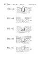
- FIG. 3is a cross-sectional vertical view of an isolation structure of a semiconductor device according to the present invention.
- FIGS. 4A through 4Eare cross-sectional vertical views illustrating a fabrication method of an isolation structure of a semiconductor device according to the present invention.
- FIG. 3is a cross-sectional vertical view illustrating an isolation structure of a semiconductor device using an insulating film according to the present invention.
- a trench 301is formed in a device isolation region in a semiconductor substrate 300 and an impurity ion segregation precluding layer 302 is formed on a surface of the semiconductor substrate 300 along a sidewall and a bottom of the trench 301 , the impurity ion segregation precluding layer 302 having a thickness of about 1-9 A.
- An insulator 303which is a silicon oxide SiO 2 or silicon nitride Si 3 N 4 is filled in the trench 301 .
- the impurity ion segregation precluding layer 302 at the thickness of 1-9 A formed along the sidewall and bottom of the trench 301prevents the impurity ions in the semiconductor substrate 300 from permeating through the insulator 303 in the trench 301 , thus preventing decrease in the impurity density of the semiconductor substrate. Accordingly, decrease in the threshold voltage in which a channel is formed below the threshold voltage is prevented and thus the reliability of the semiconductor device can improve.
- the impurity ion segregation precluding layer 302is obtained by putting the semiconductor substrate 300 having trench 301 in a high-temperature furnace (a furnace that is generally used in a semiconductor mass-production line) at about 800 ⁇ C. and annealing the semiconductor substrate 300 while flowing nitride gas into the furnace at over 20 l/min. Since the semiconductor substrate 300 is silicon and the annealing process is applied with flowing the nitride gas, the impurity ion segregation precluding layer 302 formed on the bottom and sidewall of the trench 301 of the semiconductor substrate 300 is a silicon nitride which includes silicon and nitride atoms, respectively.
- the silicon nitrideit is considered that a combination ratio of silicon to nitride is under 0.75 because of the large inflow of the nitride gas. That is, the silicon nitride has the most stable condition when three (3) silicon atoms are combined with four (4) nitride atoms such as Si 3 N 4 .
- the combination ratio of the silicon to the nitrideis not 3:4, but the ratio of the nitride atom is higher than the silicon. Accordingly, the silicon nitride according to the present invention will be referred to a nitrogen-rich silicon nitride.
- such a nitrogen-rich silicon nitridecan be Si 3 N 4.1 , Si 3 N 4.2 , Si 3 N 4.3 , Si 3 N 4.4 . . . , or Si 2.9 N 4 , Si 2.8 N 4 , Si 2.7 N 4 , Si 2.6 N 4 , that is, when the silicon atom is 3, the nitride atom is at least 4, or when the nitride atom is 4, the silicon atom is less than 3.
- the impurity ion segregation precluding layeris considerably thin, of which a thickness is less than 10 A. Since the thickness of the insulating film is less than 10 A, the insulating film is a single nitride atom layer. However, it has been observed through the experiment that the impurity ion segregation effect of this thin layer is excellent.
- the thickness of the impurity ion segregation precluding layer according to the present inventionis not a measured value but an estimated one, because “Telcor” of Telcor which the inventor used for measuring the film can only measure a film which has a thickness of at least 10 A. As a result of measuring the thickness of the impurity ion segregation precluding layer, it indicated 10 A, which is the lowest value that the instrument could measure. Thus, it is estimated that the thickness of the film is 10 A or less.
- the impurity permeation preventing filmis a silicon nitride.
- the amount of the employed nitride gasis considerably larger than the nitride gas (61 /min at its maximum), which is used for the annealing process in the semiconductor device fabrication process, it is considered to be the nitrogen-rich silicon nitride.
- the inventoradditionally carried out the following experiment to evaluate the existence of the impurity ion segregation precluding layer and the characteristics thereof.
- Table 1illustrates results of the experiment that measured a thickness of an oxide formed on the semiconductor substrate when the semiconductor substrate was placed in the furnace at a temperature of at least about 800 ⁇ C. and annealed in an oxygen atmosphere while flowing the nitride gas at 121 /min and 201 /min, respectively, thereinto.
- the thickness of the oxide formed on the silicon substrate which was obtained under the same conditions in the oxygen atmospherewas 70 A.
- the thickness of each oxide formed on the semiconductor substratewas less than 70 A.
- the oxide formed on the silicon semiconductor substratehad a thickness of 66.8 A on average through experiments of three times, which had nearly the same result as the oxide formed on the semiconductor substrate without the nitride gas inflow into the furnace.
- the oxide formed on the silicon semiconductor substratehad a thickness of 36.6 A on average through experiments of three times, which has about half the thickness of the oxide formed on the semiconductor substrate without the nitride gas inflow into the furnace. Accordingly, it can be seen that when the nitride gas was flowed at least at 201 /min during the annealing process, there is formed a film that prevents oxidization of a surface of the silicon semiconductor substrate.
- Si 3 N 4which is a stable silicon nitride.
- the oxidegrows, but the growth speed of the oxide was controlled while growing.
- the silicon nitridehas an unstable combination of a compound, not a stable one, and thus the inventor referred to the silicon nitride as the nitrogen-rich silicon nitride.
- the nitrogen-rich silicon nitrideis not sufficiently formed on the semiconductor substrate, but when the annealing process is performed with the inflow of the nitride gas into the furnace at at least 20 l/min, there is formed on the surface of the trench the nitrogen-rich silicon nitride that has a desirable effect of precluding the impurity ion segregation.
- FIGS. 4A to 4 ENext, a fabrication method of the semiconductor device isolation structure of FIG. 3 according to the present invention will be described with the reference to FIGS. 4A to 4 E.
- a trench 401is formed in a part of a semiconductor substrate 400 corresponding to a device isolation region.
- the trench 401is formed by the following process.
- a pad oxide 411is formed over the semiconductor substrate 400 .
- the pad oxide 411can be formed by oxidizing a silicon substrate by a thermal oxidization method or deposited by a chemical vapor deposition method.
- a silicon nitride 412is deposited on the pad oxide 411 , and a photoresist film (not shown) is applied on the silicon nitride 412 and a photolithography process is performed, so that the photoresist film remains on the silicon nitride 412 , which corresponds to an active region, which becomes a photoresist film pattern (not shown).
- the photoresist film patternas a mask, the silicon nitride 412 and the pad oxide 411 are etched by a reactive ion etching method and then the semiconductor substrate 400 formed under the etched pad oxide 411 is etched to a predetermined depth, thereby forming the trench 401 .
- the semiconductor substrateis annealed at 1050 ⁇ C. in an O 2 atmosphere, so that there is formed a thermal oxide 402 at a thickness of about 50-200 A on the semiconductor substrate 400 in the trench 401 .
- the thermal oxide 402is removed using an HF solution.
- the semiconductor substrate of FIG. 4 bis placed in a furnace at a temperature of at least 800 ⁇ C. and annealed while flowing a nitride gas N 2 into the furnace at 20-501 /min, thereby forming an impurity ion segregation precluding layer 403 at a thickness of 1-10 A on the semiconductor substrate 400 along an inner wall and a bottom of the trench 401 .
- the impurity ion segregation precluding layer 403is the nitrogen-rich silicon nitride which has been above described.
- a nitride ion implantation methodcan be performed as a method for forming the nitrogen-rich silicon nitride on the semiconductor substrate, however since such an ion implantation method damages the surface of the semiconductor substrate, it is not recommendable. Specifically, when a portion of the semiconductor substrate adjacent to the device isolation region is damaged, a leakage current may be generated, thus it is more desirable to perform the annealing process in the nitride atmosphere, rather than the ion implantation method.
- an insulator 404is formed on an entire surface of the resultant structure of FIG. 4C including the trench 401 and an annealing process is performed to the resultant structure.
- the insulatoris preferably a silicon oxide or silicon nitride. Then, a chemical mechanical polishing process is performed to the insulator 404 for thereby removing a portion of the insulator formed on the silicon nitride 412 , so that a surface level of the resultant semiconductor substrate 400 becomes planarized.
- the silicon nitride 412 and the pad oxide 411are sequentially removed, thereby completing the fabrication of the isolation structure of the semiconductor device.
- the thin impurity ion segregation precluding layerthat is, the nitrogen-rich silicon nitride at a thickness of several A is formed on the surface of the part of the semiconductor substrate corresponding to the device isolation region, thereby preventing the inter-permeation of the impurity ions between the device isolation region and the semiconductor substrate, which has an effect of improving the reliability of semiconductor device by stabilizing the electric characteristics of the device.
Landscapes
- Engineering & Computer Science (AREA)
- Physics & Mathematics (AREA)
- Condensed Matter Physics & Semiconductors (AREA)
- General Physics & Mathematics (AREA)
- Manufacturing & Machinery (AREA)
- Computer Hardware Design (AREA)
- Microelectronics & Electronic Packaging (AREA)
- Power Engineering (AREA)
- Element Separation (AREA)
Abstract
Description
| TABLE 1 | |||
| Experiment (time) | |||
| 1 | 2 | 3 | average | ||
| Nitride | 12 | thickness of | 66.9 | 66.5 | 67.0 | 66.8 |
| (l) | 20 | oxide(A) | 39.3 | 31.2 | 39.3 | 36.6 |
Claims (10)
Priority Applications (1)
| Application Number | Priority Date | Filing Date | Title |
|---|---|---|---|
| US10/015,665US20020123244A1 (en) | 1999-05-10 | 2001-12-17 | Impurity ion segregation precluding layer, fabrication method thereof, isolation structure for semiconductor device using the impurity ion segregation precluding layer and fabricating method thereof |
Applications Claiming Priority (2)
| Application Number | Priority Date | Filing Date | Title |
|---|---|---|---|
| KR99-16624 | 1999-05-10 | ||
| KR1019990016624AKR100319620B1 (en) | 1999-05-10 | 1999-05-10 | Isolation structure for semiconductor device and fabricating method thereof |
Related Child Applications (1)
| Application Number | Title | Priority Date | Filing Date |
|---|---|---|---|
| US10/015,665DivisionUS20020123244A1 (en) | 1999-05-10 | 2001-12-17 | Impurity ion segregation precluding layer, fabrication method thereof, isolation structure for semiconductor device using the impurity ion segregation precluding layer and fabricating method thereof |
Publications (1)
| Publication Number | Publication Date |
|---|---|
| US6337256B1true US6337256B1 (en) | 2002-01-08 |
Family
ID=19584549
Family Applications (2)
| Application Number | Title | Priority Date | Filing Date |
|---|---|---|---|
| US09/441,206Expired - LifetimeUS6337256B1 (en) | 1999-05-10 | 1999-11-16 | Impurity ion segregation precluding layer, fabrication method thereof, isolation structure for semiconductor device using the impurity ion segregation precluding layer and fabricating method thereof |
| US10/015,665AbandonedUS20020123244A1 (en) | 1999-05-10 | 2001-12-17 | Impurity ion segregation precluding layer, fabrication method thereof, isolation structure for semiconductor device using the impurity ion segregation precluding layer and fabricating method thereof |
Family Applications After (1)
| Application Number | Title | Priority Date | Filing Date |
|---|---|---|---|
| US10/015,665AbandonedUS20020123244A1 (en) | 1999-05-10 | 2001-12-17 | Impurity ion segregation precluding layer, fabrication method thereof, isolation structure for semiconductor device using the impurity ion segregation precluding layer and fabricating method thereof |
Country Status (2)
| Country | Link |
|---|---|
| US (2) | US6337256B1 (en) |
| KR (1) | KR100319620B1 (en) |
Cited By (13)
| Publication number | Priority date | Publication date | Assignee | Title |
|---|---|---|---|---|
| US20030190773A1 (en)* | 2002-04-05 | 2003-10-09 | Nec Electronics Corporation | Method for manufacturing semiconductor device using shallow trench isolation process |
| US20040155341A1 (en)* | 2002-10-31 | 2004-08-12 | Pipes Leonard C. | Implantating ions in shallow trench isolation structures |
| US20050142895A1 (en)* | 2002-09-19 | 2005-06-30 | Applied Materials, Inc. | Gap-fill depositions in the formation of silicon containing dielectric materials |
| US20060030165A1 (en)* | 2004-08-04 | 2006-02-09 | Applied Materials, Inc. A Delaware Corporation | Multi-step anneal of thin films for film densification and improved gap-fill |
| US20070059896A1 (en)* | 2002-09-19 | 2007-03-15 | Applied Materials, Inc. | Nitrous oxide anneal of teos/ozone cvd for improved gapfill |
| US20070212850A1 (en)* | 2002-09-19 | 2007-09-13 | Applied Materials, Inc. | Gap-fill depositions in the formation of silicon containing dielectric materials |
| US20070212847A1 (en)* | 2004-08-04 | 2007-09-13 | Applied Materials, Inc. | Multi-step anneal of thin films for film densification and improved gap-fill |
| US20080115726A1 (en)* | 2004-08-27 | 2008-05-22 | Applied Materials, Inc. | gap-fill depositions introducing hydroxyl-containing precursors in the formation of silicon containing dielectric materials |
| US7431967B2 (en) | 2002-09-19 | 2008-10-07 | Applied Materials, Inc. | Limited thermal budget formation of PMD layers |
| US20140064004A1 (en)* | 2012-08-31 | 2014-03-06 | SK Hynix Inc. | Semiconductor device including buried gate, module and system, and method for manufacturing |
| US9018108B2 (en) | 2013-01-25 | 2015-04-28 | Applied Materials, Inc. | Low shrinkage dielectric films |
| US9287374B2 (en)* | 2014-03-26 | 2016-03-15 | SK Hynix Inc. | Semiconductor device and method for forming the same |
| CN114388429A (en)* | 2022-01-20 | 2022-04-22 | 武汉新芯集成电路制造有限公司 | Semiconductor device, method of making the same, and image sensor |
Families Citing this family (1)
| Publication number | Priority date | Publication date | Assignee | Title |
|---|---|---|---|---|
| CN102543760B (en)* | 2012-02-28 | 2014-06-04 | 上海华力微电子有限公司 | Method for increasing shallow trench isolating compressive stress and improving NMOS electron mobility |
Citations (7)
| Publication number | Priority date | Publication date | Assignee | Title |
|---|---|---|---|---|
| US4571819A (en)* | 1984-11-01 | 1986-02-25 | Ncr Corporation | Method for forming trench isolation structures |
| US5447884A (en)* | 1994-06-29 | 1995-09-05 | International Business Machines Corporation | Shallow trench isolation with thin nitride liner |
| US5780346A (en)* | 1996-12-31 | 1998-07-14 | Intel Corporation | N2 O nitrided-oxide trench sidewalls and method of making isolation structure |
| US5985735A (en)* | 1995-09-29 | 1999-11-16 | Intel Corporation | Trench isolation process using nitrogen preconditioning to reduce crystal defects |
| US6051478A (en)* | 1997-12-18 | 2000-04-18 | Advanced Micro Devices, Inc. | Method of enhancing trench edge oxide quality |
| JP2000124303A (en)* | 1998-10-09 | 2000-04-28 | Samsung Electronics Co Ltd | Manufacturing method of trench isolation |
| US6255194B1 (en)* | 1999-06-03 | 2001-07-03 | Samsung Electronics Co., Ltd. | Trench isolation method |
Family Cites Families (2)
| Publication number | Priority date | Publication date | Assignee | Title |
|---|---|---|---|---|
| FR2681554B1 (en)* | 1991-09-23 | 1993-12-10 | Essilor Internal Cie Gle Optique | PROCESS FOR OBTAINING AN OPTICAL LENS OF THERMOPLASTIC SYNTHETIC MATERIAL COATED WITH A PROTECTIVE LAYER OF THERMOSETTING SYNTHETIC MATERIAL. |
| US5376317A (en)* | 1992-12-08 | 1994-12-27 | Galic Maus Ventures | Precision surface-replicating thermoplastic injection molding method and apparatus, using a heating phase and a cooling phase in each molding cycle |
- 1999
- 1999-05-10KRKR1019990016624Apatent/KR100319620B1/ennot_activeExpired - Fee Related
- 1999-11-16USUS09/441,206patent/US6337256B1/ennot_activeExpired - Lifetime
- 2001
- 2001-12-17USUS10/015,665patent/US20020123244A1/ennot_activeAbandoned
Patent Citations (8)
| Publication number | Priority date | Publication date | Assignee | Title |
|---|---|---|---|---|
| US4571819A (en)* | 1984-11-01 | 1986-02-25 | Ncr Corporation | Method for forming trench isolation structures |
| US5447884A (en)* | 1994-06-29 | 1995-09-05 | International Business Machines Corporation | Shallow trench isolation with thin nitride liner |
| US5985735A (en)* | 1995-09-29 | 1999-11-16 | Intel Corporation | Trench isolation process using nitrogen preconditioning to reduce crystal defects |
| US5780346A (en)* | 1996-12-31 | 1998-07-14 | Intel Corporation | N2 O nitrided-oxide trench sidewalls and method of making isolation structure |
| US6051478A (en)* | 1997-12-18 | 2000-04-18 | Advanced Micro Devices, Inc. | Method of enhancing trench edge oxide quality |
| JP2000124303A (en)* | 1998-10-09 | 2000-04-28 | Samsung Electronics Co Ltd | Manufacturing method of trench isolation |
| US6251746B1 (en)* | 1998-10-09 | 2001-06-26 | Samsung Electronics Co., Ltd. | Methods of forming trench isolation regions having stress-reducing nitride layers therein |
| US6255194B1 (en)* | 1999-06-03 | 2001-07-03 | Samsung Electronics Co., Ltd. | Trench isolation method |
Non-Patent Citations (4)
| Title |
|---|
| Genshu Fuse et al., "A New Isolation Method with Boron-Implanted Sidewalls for Controlling Narrow-Width Effect", IEEE Transactions On Electron Devices, vol. ED-34, No. 2, Feb. 1987, pp. 356-360. |
| Mazumder et al Improved Reliability of No Treated NH3-Nitrided Oxide with Regard to O2 Annealing Solid State Electronics vol. 42 No. 6 pp. 921-924 1998.* |
| T. S. Chao et al., "Mechanism of Nitrogen Coimplant for Suppressing Boron Penetration in rho+-polycrystalline Silicon Gate of rho Metal-Oxide Semiconductor Field Effect Transistor", Appl. Phys. Letters, vol. 69, No. 12, Sep. 16, 1996, pp. 1781-1782. |
| T. S. Chao et al., "Mechanism of Nitrogen Coimplant for Suppressing Boron Penetration in ρ+-polycrystalline Silicon Gate of ρ Metal-Oxide Semiconductor Field Effect Transistor", Appl. Phys. Letters, vol. 69, No. 12, Sep. 16, 1996, pp. 1781-1782. |
Cited By (19)
| Publication number | Priority date | Publication date | Assignee | Title |
|---|---|---|---|---|
| US20030190773A1 (en)* | 2002-04-05 | 2003-10-09 | Nec Electronics Corporation | Method for manufacturing semiconductor device using shallow trench isolation process |
| US20070212850A1 (en)* | 2002-09-19 | 2007-09-13 | Applied Materials, Inc. | Gap-fill depositions in the formation of silicon containing dielectric materials |
| US7674727B2 (en) | 2002-09-19 | 2010-03-09 | Applied Materials, Inc. | Nitrous oxide anneal of TEOS/ozone CVD for improved gapfill |
| US20050142895A1 (en)* | 2002-09-19 | 2005-06-30 | Applied Materials, Inc. | Gap-fill depositions in the formation of silicon containing dielectric materials |
| US7456116B2 (en) | 2002-09-19 | 2008-11-25 | Applied Materials, Inc. | Gap-fill depositions in the formation of silicon containing dielectric materials |
| US7431967B2 (en) | 2002-09-19 | 2008-10-07 | Applied Materials, Inc. | Limited thermal budget formation of PMD layers |
| US20070059896A1 (en)* | 2002-09-19 | 2007-03-15 | Applied Materials, Inc. | Nitrous oxide anneal of teos/ozone cvd for improved gapfill |
| US7061068B2 (en)* | 2002-10-31 | 2006-06-13 | Intel Corporation | Shallow trench isolation structures having uniform and smooth topography |
| US20040155341A1 (en)* | 2002-10-31 | 2004-08-12 | Pipes Leonard C. | Implantating ions in shallow trench isolation structures |
| US20070212847A1 (en)* | 2004-08-04 | 2007-09-13 | Applied Materials, Inc. | Multi-step anneal of thin films for film densification and improved gap-fill |
| US20070000897A1 (en)* | 2004-08-04 | 2007-01-04 | Applied Materials, Inc. | Multi-step anneal of thin films for film densification and improved gap-fill |
| US20060030165A1 (en)* | 2004-08-04 | 2006-02-09 | Applied Materials, Inc. A Delaware Corporation | Multi-step anneal of thin films for film densification and improved gap-fill |
| US7642171B2 (en) | 2004-08-04 | 2010-01-05 | Applied Materials, Inc. | Multi-step anneal of thin films for film densification and improved gap-fill |
| US20080115726A1 (en)* | 2004-08-27 | 2008-05-22 | Applied Materials, Inc. | gap-fill depositions introducing hydroxyl-containing precursors in the formation of silicon containing dielectric materials |
| WO2007118196A1 (en)* | 2006-04-07 | 2007-10-18 | Applied Materials, Inc. | Multi-step anneal of thin films for film densification and improved gap-fill |
| US20140064004A1 (en)* | 2012-08-31 | 2014-03-06 | SK Hynix Inc. | Semiconductor device including buried gate, module and system, and method for manufacturing |
| US9018108B2 (en) | 2013-01-25 | 2015-04-28 | Applied Materials, Inc. | Low shrinkage dielectric films |
| US9287374B2 (en)* | 2014-03-26 | 2016-03-15 | SK Hynix Inc. | Semiconductor device and method for forming the same |
| CN114388429A (en)* | 2022-01-20 | 2022-04-22 | 武汉新芯集成电路制造有限公司 | Semiconductor device, method of making the same, and image sensor |
Also Published As
| Publication number | Publication date |
|---|---|
| KR20000073373A (en) | 2000-12-05 |
| US20020123244A1 (en) | 2002-09-05 |
| KR100319620B1 (en) | 2002-01-05 |
Similar Documents
| Publication | Publication Date | Title |
|---|---|---|
| US6627512B2 (en) | Method of manufacturing a semiconductor device | |
| US5933748A (en) | Shallow trench isolation process | |
| US5410176A (en) | Integrated circuit with planarized shallow trench isolation | |
| US5151381A (en) | Method for local oxidation of silicon employing two oxidation steps | |
| US5789769A (en) | Semiconductor device having an improved trench isolation | |
| US6337256B1 (en) | Impurity ion segregation precluding layer, fabrication method thereof, isolation structure for semiconductor device using the impurity ion segregation precluding layer and fabricating method thereof | |
| US6953734B2 (en) | Method for manufacturing shallow trench isolation in semiconductor device | |
| JPH11111710A (en) | Semiconductor device and its manufacture | |
| KR100363558B1 (en) | Method of forming a trench isolation in an integrated circuit device | |
| US5716891A (en) | Fabrication process of semiconductor device | |
| JP4363564B2 (en) | Method for forming element isolation film of semiconductor element | |
| US6448149B1 (en) | Method for making shallow trench isolation in semiconductor fabrication | |
| EP1000439B1 (en) | Method of forming side dielectrically isolated semiconductor devices | |
| US5972777A (en) | Method of forming isolation by nitrogen implant to reduce bird's beak | |
| JPH07201978A (en) | Method for isolating semiconductor elements from each other | |
| US6670690B1 (en) | Method of making an improved field oxide isolation structure for semiconductor integrated circuits having higher field oxide threshold voltages | |
| US6455391B1 (en) | Method of forming structures with buried regions in a semiconductor device | |
| JPH08125010A (en) | Isolation structure of semiconductor device and formation thereof | |
| KR100381493B1 (en) | Semiconductor device and manufacturing method thereof | |
| KR100549974B1 (en) | Method of manufacturing bipolar and bismos devices | |
| KR100540340B1 (en) | Method For Manufacturing Semiconductor Devices | |
| US6969666B2 (en) | Method for fabricating isolation layer in semiconductor device | |
| KR20000044560A (en) | Method for forming trench isolation film of semiconductor device | |
| KR0167231B1 (en) | Isolation method for semiconductor device | |
| KR19990074005A (en) | Trench Device Isolation Method to Prevent Impurity Diffusion from Well Area |
Legal Events
| Date | Code | Title | Description |
|---|---|---|---|
| AS | Assignment | Owner name:HYUNDAI ELECTRONICS INDUSTRIES CO., LTD., KOREA, R Free format text:ASSIGNMENT OF ASSIGNORS INTEREST;ASSIGNOR:SHIM, HYUN SOOK;REEL/FRAME:010398/0540 Effective date:19991101 | |
| AS | Assignment | Owner name:HYUNDAI ELECTRONICS INDUSTRIES, CO., LTD., KOREA, Free format text:MERGER;ASSIGNOR:LG SEMICON CO., LTD.;REEL/FRAME:010951/0606 Effective date:19991020 | |
| FEPP | Fee payment procedure | Free format text:PAYOR NUMBER ASSIGNED (ORIGINAL EVENT CODE: ASPN); ENTITY STATUS OF PATENT OWNER: LARGE ENTITY | |
| STCF | Information on status: patent grant | Free format text:PATENTED CASE | |
| FPAY | Fee payment | Year of fee payment:4 | |
| FPAY | Fee payment | Year of fee payment:8 | |
| FEPP | Fee payment procedure | Free format text:PAYER NUMBER DE-ASSIGNED (ORIGINAL EVENT CODE: RMPN); ENTITY STATUS OF PATENT OWNER: LARGE ENTITY Free format text:PAYOR NUMBER ASSIGNED (ORIGINAL EVENT CODE: ASPN); ENTITY STATUS OF PATENT OWNER: LARGE ENTITY | |
| AS | Assignment | Owner name:HYNIX SEMICONDUCTOR INC., KOREA, REPUBLIC OF Free format text:CHANGE OF NAME;ASSIGNOR:HYUNDAI ELECTRONICS INDUSTRIES CO., LTD.;REEL/FRAME:026828/0688 Effective date:20010329 | |
| AS | Assignment | Owner name:658868 N.B. INC., CANADA Free format text:ASSIGNMENT OF ASSIGNORS INTEREST;ASSIGNOR:HYNIX SEMICONDUCTOR INC.;REEL/FRAME:027234/0693 Effective date:20110822 | |
| AS | Assignment | Owner name:ROYAL BANK OF CANADA, CANADA Free format text:U.S. INTELLECTUAL PROPERTY SECURITY AGREEMENT (FOR NON-U.S. GRANTORS) - SHORT FORM;ASSIGNORS:658276 N.B. LTD.;658868 N.B. INC.;MOSAID TECHNOLOGIES INCORPORATED;REEL/FRAME:027512/0196 Effective date:20111223 | |
| FPAY | Fee payment | Year of fee payment:12 | |
| AS | Assignment | Owner name:CONVERSANT IP N.B. 868 INC., CANADA Free format text:CHANGE OF NAME;ASSIGNOR:658868 N.B. INC.;REEL/FRAME:032439/0547 Effective date:20140101 | |
| AS | Assignment | Owner name:CONVERSANT INTELLECTUAL PROPERTY MANAGEMENT INC., Free format text:RELEASE OF SECURITY INTEREST;ASSIGNOR:ROYAL BANK OF CANADA;REEL/FRAME:033484/0344 Effective date:20140611 Owner name:CONVERSANT IP N.B. 868 INC., CANADA Free format text:RELEASE OF SECURITY INTEREST;ASSIGNOR:ROYAL BANK OF CANADA;REEL/FRAME:033484/0344 Effective date:20140611 Owner name:CONVERSANT IP N.B. 276 INC., CANADA Free format text:RELEASE OF SECURITY INTEREST;ASSIGNOR:ROYAL BANK OF CANADA;REEL/FRAME:033484/0344 Effective date:20140611 | |
| AS | Assignment | Owner name:CPPIB CREDIT INVESTMENTS INC., AS LENDER, CANADA Free format text:U.S. PATENT SECURITY AGREEMENT (FOR NON-U.S. GRANTORS);ASSIGNOR:CONVERSANT IP N.B. 868 INC.;REEL/FRAME:033707/0001 Effective date:20140611 Owner name:ROYAL BANK OF CANADA, AS LENDER, CANADA Free format text:U.S. PATENT SECURITY AGREEMENT (FOR NON-U.S. GRANTORS);ASSIGNOR:CONVERSANT IP N.B. 868 INC.;REEL/FRAME:033707/0001 Effective date:20140611 | |
| AS | Assignment | Owner name:CONVERSANT INTELLECTUAL PROPERTY MANAGEMENT INC., Free format text:ASSIGNMENT OF ASSIGNORS INTEREST;ASSIGNOR:CONVERSANT IP N.B. 868 INC.;REEL/FRAME:036159/0386 Effective date:20150514 | |
| AS | Assignment | Owner name:CPPIB CREDIT INVESTMENTS, INC., CANADA Free format text:AMENDED AND RESTATED U.S. PATENT SECURITY AGREEMENT (FOR NON-U.S. GRANTORS);ASSIGNOR:CONVERSANT INTELLECTUAL PROPERTY MANAGEMENT INC.;REEL/FRAME:046900/0136 Effective date:20180731 | |
| AS | Assignment | Owner name:CONVERSANT INTELLECTUAL PROPERTY MANAGEMENT INC., CANADA Free format text:RELEASE OF U.S. PATENT AGREEMENT (FOR NON-U.S. GRANTORS);ASSIGNOR:ROYAL BANK OF CANADA, AS LENDER;REEL/FRAME:047645/0424 Effective date:20180731 Owner name:CONVERSANT INTELLECTUAL PROPERTY MANAGEMENT INC., Free format text:RELEASE OF U.S. PATENT AGREEMENT (FOR NON-U.S. GRANTORS);ASSIGNOR:ROYAL BANK OF CANADA, AS LENDER;REEL/FRAME:047645/0424 Effective date:20180731 | |
| AS | Assignment | Owner name:CONVERSANT INTELLECTUAL PROPERTY MANAGEMENT INC., CANADA Free format text:RELEASE BY SECURED PARTY;ASSIGNOR:CPPIB CREDIT INVESTMENTS INC.;REEL/FRAME:054371/0884 Effective date:20201028 |