US6336160B1 - Method and system for dividing a computer processor register into sectors and storing frequently used values therein - Google Patents
Method and system for dividing a computer processor register into sectors and storing frequently used values thereinDownload PDFInfo
- Publication number
- US6336160B1 US6336160B1US09/100,717US10071798AUS6336160B1US 6336160 B1US6336160 B1US 6336160B1US 10071798 AUS10071798 AUS 10071798AUS 6336160 B1US6336160 B1US 6336160B1
- Authority
- US
- United States
- Prior art keywords
- sectors
- value
- register
- sector
- memory device
- Prior art date
- Legal status (The legal status is an assumption and is not a legal conclusion. Google has not performed a legal analysis and makes no representation as to the accuracy of the status listed.)
- Expired - Lifetime
Links
Images


Classifications
- G—PHYSICS
- G06—COMPUTING OR CALCULATING; COUNTING
- G06F—ELECTRIC DIGITAL DATA PROCESSING
- G06F9/00—Arrangements for program control, e.g. control units
- G06F9/06—Arrangements for program control, e.g. control units using stored programs, i.e. using an internal store of processing equipment to receive or retain programs
- G06F9/30—Arrangements for executing machine instructions, e.g. instruction decode
- G06F9/30098—Register arrangements
- G06F9/30105—Register structure
- G06F9/30112—Register structure comprising data of variable length
- G—PHYSICS
- G06—COMPUTING OR CALCULATING; COUNTING
- G06F—ELECTRIC DIGITAL DATA PROCESSING
- G06F9/00—Arrangements for program control, e.g. control units
- G06F9/06—Arrangements for program control, e.g. control units using stored programs, i.e. using an internal store of processing equipment to receive or retain programs
- G06F9/30—Arrangements for executing machine instructions, e.g. instruction decode
- G06F9/30098—Register arrangements
- G06F9/30105—Register structure
- G06F9/30109—Register structure having multiple operands in a single register
- G—PHYSICS
- G06—COMPUTING OR CALCULATING; COUNTING
- G06F—ELECTRIC DIGITAL DATA PROCESSING
- G06F9/00—Arrangements for program control, e.g. control units
- G06F9/06—Arrangements for program control, e.g. control units using stored programs, i.e. using an internal store of processing equipment to receive or retain programs
- G06F9/30—Arrangements for executing machine instructions, e.g. instruction decode
- G06F9/30098—Register arrangements
- G06F9/3012—Organisation of register space, e.g. banked or distributed register file
- G06F9/30138—Extension of register space, e.g. register cache
- G—PHYSICS
- G06—COMPUTING OR CALCULATING; COUNTING
- G06F—ELECTRIC DIGITAL DATA PROCESSING
- G06F9/00—Arrangements for program control, e.g. control units
- G06F9/06—Arrangements for program control, e.g. control units using stored programs, i.e. using an internal store of processing equipment to receive or retain programs
- G06F9/30—Arrangements for executing machine instructions, e.g. instruction decode
- G06F9/38—Concurrent instruction execution, e.g. pipeline or look ahead
- G06F9/3824—Operand accessing
- G06F9/383—Operand prefetching
- G06F9/3832—Value prediction for operands; operand history buffers
- G—PHYSICS
- G06—COMPUTING OR CALCULATING; COUNTING
- G06F—ELECTRIC DIGITAL DATA PROCESSING
- G06F9/00—Arrangements for program control, e.g. control units
- G06F9/06—Arrangements for program control, e.g. control units using stored programs, i.e. using an internal store of processing equipment to receive or retain programs
- G06F9/30—Arrangements for executing machine instructions, e.g. instruction decode
- G06F9/38—Concurrent instruction execution, e.g. pipeline or look ahead
- G06F9/3836—Instruction issuing, e.g. dynamic instruction scheduling or out of order instruction execution
- G06F9/3838—Dependency mechanisms, e.g. register scoreboarding
- G06F9/384—Register renaming
Definitions
- the present inventionrelates generally to information handling systems and more particularly to an improved methodology for referencing information in registers of computer processing units.
- register renamingrefers to a method by which a specific processor register may be used by multiple instructions without conflict. For example, if an instruction requires the use of a specific register, and a second instruction also requires the use of that same register while the register is still being used by the first instruction, the processor will redefine one of its unused registers as a second copy of the specific register, and the processor will track and manage the specific register and the renamed register relative to the information contained in the registers and the associated instructions.
- Register renamingcan also be used to redirect data held over in a rename register from the execution of a previous instruction for use by a subsequent instruction.
- reuse of data values in rename registersis practically not achievable because rename registers get written over by new data values before the older values can be reused.
- Processorsonly have a very limited number of rename registers and adding too many such registers have other implementation performance-limiting aspects.
- processorshave implemented register addressing on a whole unit basis. That is, register renaming is done by assigning an alias code to each operand on the basis of the register identifier and without regard to the portion of the bits of that register which are actually accessed by the instruction. This practice results in a waste of precious register bits.
- a method and apparatusis provided for sectoring processor registers and utilizing the most significant unused sectors of the processor registers to hold frequently used data. Since most register data values do not utilize the most significant bits of a register value, these most significant bits grouped as sectors can be utilized to provide enhanced performance resulting from data buffering. Unused register sectors are used to hold frequently used data or sequentially adjacent data to exploit spatial locality, thus, saving processor cycles to fetch data from the processor memory.
- the register fileis divided into sectors such that the smallest accessible unit for an instruction set in each register can be uniquely addressed and renamed.
- the most significant sectors of the registersif not marked to be in use, are used for holding pre-assigned constant values, such as “0”, “1”, or other frequently used constant offsets, etc.
- the previous data loaded into register sectorsis saved in most significant register sectors for future possible reference by subsequent instructions.
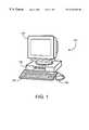
- FIG. 1is a diagram of a partial simplified exemplary computer system in which the present invention may be implemented
- FIG. 2is a high level block diagram showing selected components and subsystems within the exemplary system illustrated in FIG. 1;
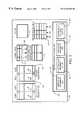
- FIG. 3is a block diagram illustrating in greater detail selected components within the central processing unit (CPU) of FIG. 2;
- FIG. 4is a flowchart illustrating an operational sequence for a register used as a source register in the processing of an instruction
- FIG. 5is a flowchart illustrating an operational sequence for a register used as a target register in the processing of an instruction.
- FIG. 6is a flowchart illustrating in more detail the operational sequence for determining buffered value matches shown in FIG. 5 .
- FIG. 1presents a portion of an exemplary computer system in which the present invention may be implemented.
- a computer station 100includes a CPU (central processing unit) enclosure 102 that typically encloses much of the electronics of the system.
- a keyboard 104 and a pointing device or “mouse” 106are arranged to receive inputs to the system from an operator. These operator inputs may be responsive to programmed presentations appearing on a display device 108 .
- the display device 108is shown as a cathode ray tube (CRT) in the present example although other display devices such as liquid crystal displays (LCDs) or active matrix displays typically used with portable systems may also be implemented.
- CTRcathode ray tube
- LCDsliquid crystal displays
- active matrix displaystypically used with portable systems may also be implemented.
- the present inventionmay be used in desktop, laptop, workstation or larger systems as well.
- a CPU chip or integrated circuit 201is shown connected to a main bus 203 .
- main bus 203For the sake of simplicity and in order not to unduly obfuscate the teachings disclosed herein, the example presented shows only a single bus although it is understood that the implementing system may include a plurality of busses and connecting bridge circuits and networks.
- a RAM (random access memory) unit 205 and a ROM (read only memory) unit 207are connected to the bus 203 .
- the bus 203is also coupled to various system controllers including a diskette controller 209 for controlling one or more floppy diskettes, a serial controller 211 typically used in communication functions, and a disk controller 213 for controlling one or more hard drive devices.
- a network interface 215is also illustrated as being connected to the bus 203 .
- the network interface 215may couple the system shown to a hardwired network or through a modem to a more extensive network such as the Internet. Further the bus 203 may be extended as shown by line 214 to include other connections to even more system devices and functional subsystems.
- the bus 203is also arranged for connection to a keyboard/mouse controller 216 , a DMA (direct memory access) controller 217 , a display controller 219 for interfacing with one or more display devices, and a parallel controller 221 typically used for connection to one or more printer devices.
- the bus 203may include adapter slots 223 for being coupled with adapter devices, and a mass memory controller 225 for use in controlling mass memory that may be, for example compact disc, read-only memory (CD-ROM) or other large scale memory devices.
- CPU 201fetches, decodes and executes instructions and transfers information to and from other system resources, such as system RAM 205 , controller 209 , etc., which are coupled to the system bus 203 or coupled through corresponding bus systems in more extensive arrangements.
- the CPU 201includes an Architected Register File (ARF) 301 , which is 64 bits wide in the present example although other sizes may also be implemented.
- the ARF 301is further divided into two 32-bit sectors designated Sector A 305 and Sector B 307 . As shown, the registers are divided into only two 32-bit sectors although smaller sectors are also possible.
- the individual registers in the register file 301are designated “R 1 ” through “RN”.
- the CPU 201further includes a second register file designated the Rename Register File (RRF) 303 .
- the RRF 303is also divided into two 32-bit sectors designated Sector A 309 and Sector B 311 . As shown, the registers are divided into only two 32-bit sectors although smaller sectors are also possible.
- the individual registers in the RRF 303are designated “RR 1 ” through “RRN”.
- Each sector A 309 and sector B 311provides an independent 32-bit rename register as shown, such as RR 1 A and RR 1 B.
- the CPUalso includes a Rename Table 313 , a Look-Up Table for Buffered Values 314 , a cache memory 315 , and a Sector Status Table 317 .
- An Instruction Processing Unit 319is also illustrated.
- the Instruction Processing Unit 319includes a Fixed Point Arithmetic Unit 321 , a Floating Point Arithmetic Unit # 1 323 , a Load Store Arithmetic Unit 325 and a Floating Point Arithmetic Unit # 2 327 , in the present example.
- the use and implementation of the ARF 301 , internal cache 315 , and Instruction Processing Unit 319are well known in the art.
- the RRF 303has typically been used for allowing the CPU 201 to execute instructions in a non-sequential fashion, often referred to as “out-of-order”, via the use of additional registers contained therein.
- a typical operation of circuitry similar to that illustrated in FIG. 3is explained in greater detail in U.S. Pat. No. 5,652,774, which is assigned to the assignee of the present invention and which is included herein by reference.
- the ARF 301 and the RRF 303are divided into two 32-bit sectors and the CPU further includes a Rename Table 313 and a Sector Status Table 317 .
- An exemplary implementation of the register renaming methodology disclosed hereinconsists of an architecture that uses 64-bit registers.
- the registeris renamed on a sector by sector basis instead of on a full register level.
- Status bitsare associated with each 32-bit halves or sectors of the register. The status indicates whether the sector has been modified, or is not changed by a particular instruction. When manipulating entire registers, all sectors are marked with the same status and the hardware operates in the usual manner. When sectors are manipulated, it is clear from the sector status bit or bits, which parts are modified and which are not. If the entire register is modified by an instruction, two rename registers are used. If the instruction modifies only one sector, then only one rename register is used.
- the renaming register pooli.e. the group of registers available for renaming, consists of a number of 32-bit registers. These rename registers are used independently for each 32-bit register sector that needs to be renamed. This pool consists of the A sector 309 and the B sector 311 in RRF 303 , and the A sector 305 sector in ARF 301 .
- the processor's 64-bit registersare divided into two sectors, each most significant (left half) and the least significant (right-half) sector can be considered as an independent register if all the register bits are not in use by the instructions.
- the most significant unused sectorscan now be preset to constant values, such as “0”, “1”, “ ⁇ 1”, “4”, “16”, etc., which are some of the constant data values that are frequently loaded into registers to perform array index operations, zero memory locations, increment counts, etc.
- the processor hardwarewill detect that the required value is already in a register sector. In that case, the processor circuitry will nullify that instruction and rename the subsequent instruction that uses the target register to the sector that is found to have that constant value. This saves an instruction from being executed and helps avoid a performance limiting memory reference for the data as well.
- most significant sectors that are not marked as usedare utilized to hold previously fetched data values that are to be overwritten by a subsequent instruction that requires a previously used register as its target register. Since, architecturally, there are only a finite number of registers, compilers reuse registers and, hence, overwrite a data value even though it may be referenced later. However, in the exemplary method illustrated here, whenever the old data value is to be overwritten, it is moved into the most significant sector of that register. If later a processor is sent an instruction to reload a data value that already exists in a sector, that instruction is nullified and the sector is renamed to the register that would have been the target of the nullified instruction. This again saves an instruction from being executed and helps avoid a performance limiting memory reference for the data as well.
- the “A” sector or the most significant sector of the ARF 301is the only sector available for renaming from the architected registers, i.e. the least significant sector 305 of the register 301 is not used for renaming.
- the first column 331 in the Rename Table 313contains the architected register number
- the second column 333contains the instruction address
- the third column 335contains the architected register or rename register number plus the sector mask. There is one sector mask bit for each sector.
- the Sector Status Table 317there is one entry per register.
- the first column 337 of the Sector Status Table 317contains the sign extend bit
- the second column 339contains the sector use bits (of which there is one bit for each sector)
- the third column 341contains the register number.
- the look-up table 314is an associative table that provides a relation between an effective address and the register sector buffering the data value of that effective address.
- FIG. 4is a flowchart illustrating an operational sequence for a register used as a source register in the processing of an instruction.
- an instructionis fetched (box 403 ) and decoded (box 405 ).
- the source registeris then fetched (box 407 ) and a decision is made to determine if the register number has been renamed (diamond 409 ). This decision is made by determining whether the register number is listed in the rename table 313 and the current instruction address is greater than the address in the rename table.
- the processcontinues by fetching (box 413 ) valid sectors from the architected registers in ARF 301 or renamed registers in RRF 303 in accordance with the Sector Status Table 317 . If the source register was renamed (diamond 409 ) then the process selects the rename register (box 411 ) and then proceeds to fetching the valid sectors (box 413 ). Next, a determination is made (diamond 415 ) as to whether to sign-extend the number 337 as determined from the Sector Status Table 317 . In not, a register value is provided (box 419 ) to the execution unit (not shown) in the CPU 201 .
- FIG. 5is a flowchart illustrating an operational sequence for a register used as a target register in the processing of an instruction. As the process is initiated (oval 501 ), an instruction is fetched (box 503 ), and decoded (box 505 ).
- FIG. 6is a flowchart illustrating in more detail the operational sequence for determining buffered value matches shown in FIG. 5 . Referring to FIGS. 5 and 6, next a check is made of the Look-Up Table (oval 506 ) for Buffered Values 314 to determine is there is a match (diamond 603 ) in the buffer table for the effective address.
- Oval 506Look-Up Table
- the rename registerwill use (box 605 ) the register and sector with the buffered value, and the rename table will be updated.
- the instructionwill be nullified (box 607 ) and the process ends (oval 61 1 ). If there is no match (diamond 603 ) the process returns (oval 609 ) to the flow illustrated in FIG. 5 .
- the target registeris then reserved (box 507 ).
- the number of sectors required to be used for the operandis determined (box 509 ).
- it is determined (box 511 )is the target is architected register's sector is being used per the Sector Status Table 317 . It is noted that only the least significant sector is used for the architected register's used in an instruction and the remaining sectors are used for renaming. If the target architected register's sector is not being used, then the process continues to set status bits of the sectors to be used (box 519 ). If the target architected sector is being used (box 51 1 ), then it is determined (diamond 512 ) if there is any outstanding instruction ( 01 ) using the register.
- the processcontinues to set status bits (box 519 ). If (diamond 512 ) there is an outstanding instruction using the register, then it is determined if the architected or rename register sector is available (box 513 ). If the sector is not available (box 513 ), the process stalls issuance of the instruction (box 515 ) until it becomes available. If the architected or rename register is available (box 513 ), then the Rename Table 313 is updated (box 517 ) with the register number 331 , instruction address 333 and Rename Register plus sector mask 335 (shown in FIG.
Landscapes
- Engineering & Computer Science (AREA)
- Software Systems (AREA)
- Theoretical Computer Science (AREA)
- Physics & Mathematics (AREA)
- General Engineering & Computer Science (AREA)
- General Physics & Mathematics (AREA)
- Executing Machine-Instructions (AREA)
Abstract
Description
Claims (7)
Priority Applications (1)
| Application Number | Priority Date | Filing Date | Title |
|---|---|---|---|
| US09/100,717US6336160B1 (en) | 1998-06-19 | 1998-06-19 | Method and system for dividing a computer processor register into sectors and storing frequently used values therein |
Applications Claiming Priority (1)
| Application Number | Priority Date | Filing Date | Title |
|---|---|---|---|
| US09/100,717US6336160B1 (en) | 1998-06-19 | 1998-06-19 | Method and system for dividing a computer processor register into sectors and storing frequently used values therein |
Publications (1)
| Publication Number | Publication Date |
|---|---|
| US6336160B1true US6336160B1 (en) | 2002-01-01 |
Family
ID=22281175
Family Applications (1)
| Application Number | Title | Priority Date | Filing Date |
|---|---|---|---|
| US09/100,717Expired - LifetimeUS6336160B1 (en) | 1998-06-19 | 1998-06-19 | Method and system for dividing a computer processor register into sectors and storing frequently used values therein |
Country Status (1)
| Country | Link |
|---|---|
| US (1) | US6336160B1 (en) |
Cited By (5)
| Publication number | Priority date | Publication date | Assignee | Title |
|---|---|---|---|---|
| US6959342B1 (en)* | 2003-08-18 | 2005-10-25 | Cray, Inc. | Replicating kernel data that is read mostly and write rarely |
| US20080215861A1 (en)* | 2003-09-08 | 2008-09-04 | Aamodt Tor M | Method and apparatus for efficient resource utilization for prescient instruction prefetch |
| US20190354371A1 (en)* | 2016-04-14 | 2019-11-21 | International Business Machines Corporation | Dentifying and tracking frequently accessed registers in a processor |
| US20220237123A1 (en)* | 2016-12-12 | 2022-07-28 | Intel Corporation | Apparatuses and methods for a processor architecture |
| US20240192959A1 (en)* | 2022-12-12 | 2024-06-13 | Arm Limited | Register renaming |
Citations (18)
| Publication number | Priority date | Publication date | Assignee | Title |
|---|---|---|---|---|
| US5497499A (en) | 1992-03-31 | 1996-03-05 | Seiko Epson Corporation | Superscalar risc instruction scheduling |
| US5519841A (en) | 1992-11-12 | 1996-05-21 | Digital Equipment Corporation | Multi instruction register mapper |
| US5524262A (en) | 1993-09-30 | 1996-06-04 | Intel Corporation | Apparatus and method for renaming registers in a processor and resolving data dependencies thereof |
| US5560032A (en) | 1991-07-08 | 1996-09-24 | Seiko Epson Corporation | High-performance, superscalar-based computer system with out-of-order instruction execution and concurrent results distribution |
| US5574928A (en) | 1993-10-29 | 1996-11-12 | Advanced Micro Devices, Inc. | Mixed integer/floating point processor core for a superscalar microprocessor with a plurality of operand buses for transferring operand segments |
| US5581717A (en) | 1994-03-01 | 1996-12-03 | Intel Corporation | Decoding circuit and method providing immediate data for a micro-operation issued from a decoder |
| US5590295A (en) | 1992-12-31 | 1996-12-31 | Seiko Epson Corporation | System and method for register renaming |
| US5590352A (en) | 1994-04-26 | 1996-12-31 | Advanced Micro Devices, Inc. | Dependency checking and forwarding of variable width operands |
| US5596731A (en) | 1995-04-21 | 1997-01-21 | Cyrix Corporation | Single clock bus transfers during burst and non-burst cycles |
| US5600848A (en) | 1993-10-21 | 1997-02-04 | Sun Microsystems, Inc. | Counterflow pipeline processor with instructions flowing in a first direction and instruction results flowing in the reverse direction |
| US5611071A (en)* | 1995-04-19 | 1997-03-11 | Cyrix Corporation | Split replacement cycles for sectored cache lines in a 64-bit microprocessor interfaced to a 32-bit bus architecture |
| US5613151A (en)* | 1994-05-19 | 1997-03-18 | Dockser; Kenneth A. | Data processor with flexible register mapping scheme |
| US5630149A (en)* | 1993-10-18 | 1997-05-13 | Cyrix Corporation | Pipelined processor with register renaming hardware to accommodate multiple size registers |
| US5652774A (en)* | 1996-07-08 | 1997-07-29 | International Business Machines Corporation | Method and apparatus for decreasing the cycle times of a data processing system |
| US5826070A (en)* | 1996-08-30 | 1998-10-20 | International Business Machines Corporation | Apparatus and method for maintaining status flags and condition codes using a renaming technique in an out of order floating point execution unit |
| US5897665A (en)* | 1995-12-15 | 1999-04-27 | Intel Corporation | Register addressing for register-register architectures used for microprocessors and microcontrollers |
| US5946718A (en)* | 1997-05-30 | 1999-08-31 | National Semiconductor Corporation | Shadow translation look-aside buffer and method of operation |
| US5946716A (en)* | 1996-05-30 | 1999-08-31 | Hewlett-Packard Company | Sectored virtual memory management system and translation look-aside buffer (TLB) for the same |
- 1998
- 1998-06-19USUS09/100,717patent/US6336160B1/ennot_activeExpired - Lifetime
Patent Citations (19)
| Publication number | Priority date | Publication date | Assignee | Title |
|---|---|---|---|---|
| US5560032A (en) | 1991-07-08 | 1996-09-24 | Seiko Epson Corporation | High-performance, superscalar-based computer system with out-of-order instruction execution and concurrent results distribution |
| US5497499A (en) | 1992-03-31 | 1996-03-05 | Seiko Epson Corporation | Superscalar risc instruction scheduling |
| US5519841A (en) | 1992-11-12 | 1996-05-21 | Digital Equipment Corporation | Multi instruction register mapper |
| US5590295A (en) | 1992-12-31 | 1996-12-31 | Seiko Epson Corporation | System and method for register renaming |
| US5524262A (en) | 1993-09-30 | 1996-06-04 | Intel Corporation | Apparatus and method for renaming registers in a processor and resolving data dependencies thereof |
| US5548776A (en) | 1993-09-30 | 1996-08-20 | Intel Corporation | N-wide bypass for data dependencies within register alias table |
| US5630149A (en)* | 1993-10-18 | 1997-05-13 | Cyrix Corporation | Pipelined processor with register renaming hardware to accommodate multiple size registers |
| US5600848A (en) | 1993-10-21 | 1997-02-04 | Sun Microsystems, Inc. | Counterflow pipeline processor with instructions flowing in a first direction and instruction results flowing in the reverse direction |
| US5574928A (en) | 1993-10-29 | 1996-11-12 | Advanced Micro Devices, Inc. | Mixed integer/floating point processor core for a superscalar microprocessor with a plurality of operand buses for transferring operand segments |
| US5581717A (en) | 1994-03-01 | 1996-12-03 | Intel Corporation | Decoding circuit and method providing immediate data for a micro-operation issued from a decoder |
| US5590352A (en) | 1994-04-26 | 1996-12-31 | Advanced Micro Devices, Inc. | Dependency checking and forwarding of variable width operands |
| US5613151A (en)* | 1994-05-19 | 1997-03-18 | Dockser; Kenneth A. | Data processor with flexible register mapping scheme |
| US5611071A (en)* | 1995-04-19 | 1997-03-11 | Cyrix Corporation | Split replacement cycles for sectored cache lines in a 64-bit microprocessor interfaced to a 32-bit bus architecture |
| US5596731A (en) | 1995-04-21 | 1997-01-21 | Cyrix Corporation | Single clock bus transfers during burst and non-burst cycles |
| US5897665A (en)* | 1995-12-15 | 1999-04-27 | Intel Corporation | Register addressing for register-register architectures used for microprocessors and microcontrollers |
| US5946716A (en)* | 1996-05-30 | 1999-08-31 | Hewlett-Packard Company | Sectored virtual memory management system and translation look-aside buffer (TLB) for the same |
| US5652774A (en)* | 1996-07-08 | 1997-07-29 | International Business Machines Corporation | Method and apparatus for decreasing the cycle times of a data processing system |
| US5826070A (en)* | 1996-08-30 | 1998-10-20 | International Business Machines Corporation | Apparatus and method for maintaining status flags and condition codes using a renaming technique in an out of order floating point execution unit |
| US5946718A (en)* | 1997-05-30 | 1999-08-31 | National Semiconductor Corporation | Shadow translation look-aside buffer and method of operation |
Cited By (9)
| Publication number | Priority date | Publication date | Assignee | Title |
|---|---|---|---|---|
| US6959342B1 (en)* | 2003-08-18 | 2005-10-25 | Cray, Inc. | Replicating kernel data that is read mostly and write rarely |
| US20080215861A1 (en)* | 2003-09-08 | 2008-09-04 | Aamodt Tor M | Method and apparatus for efficient resource utilization for prescient instruction prefetch |
| US7818547B2 (en)* | 2003-09-08 | 2010-10-19 | Intel Corporation | Method and apparatus for efficient resource utilization for prescient instruction prefetch |
| US20190354371A1 (en)* | 2016-04-14 | 2019-11-21 | International Business Machines Corporation | Dentifying and tracking frequently accessed registers in a processor |
| US10949202B2 (en)* | 2016-04-14 | 2021-03-16 | International Business Machines Corporation | Identifying and tracking frequently accessed registers in a processor |
| US20220237123A1 (en)* | 2016-12-12 | 2022-07-28 | Intel Corporation | Apparatuses and methods for a processor architecture |
| US12130740B2 (en)* | 2016-12-12 | 2024-10-29 | Intel Corporation | Apparatuses and methods for a processor architecture |
| US20240192959A1 (en)* | 2022-12-12 | 2024-06-13 | Arm Limited | Register renaming |
| US12182575B2 (en)* | 2022-12-12 | 2024-12-31 | Arm Limited | Performance monitoring information informed register renaming |
Similar Documents
| Publication | Publication Date | Title |
|---|---|---|
| KR100592122B1 (en) | Processor configured to map logical register numbers to physical register numbers using virtual register numbers | |
| US5944815A (en) | Microprocessor configured to execute a prefetch instruction including an access count field defining an expected number of access | |
| US10042814B2 (en) | System and method for using a mask register to track progress of gathering and scattering elements between data registers and memory | |
| US10387151B2 (en) | Processor and method for tracking progress of gathering/scattering data element pairs in different cache memory banks | |
| US6052769A (en) | Method and apparatus for moving select non-contiguous bytes of packed data in a single instruction | |
| US6173393B1 (en) | System for writing select non-contiguous bytes of data with single instruction having operand identifying byte mask corresponding to respective blocks of packed data | |
| US6321326B1 (en) | Prefetch instruction specifying destination functional unit and read/write access mode | |
| EP0138419B1 (en) | Central processing unit for a digital computer | |
| KR100335745B1 (en) | High performance speculative misaligned load operations | |
| US5644746A (en) | Data processing apparatus with improved mechanism for executing register-to-register transfer instructions | |
| KR20010073182A (en) | Mechanism for store to load forwarding | |
| US6240506B1 (en) | Expanding instructions with variable-length operands to a fixed length | |
| JP3609552B2 (en) | Central processing unit and computer system having non-cacheable repetitive operation instructions | |
| US6460132B1 (en) | Massively parallel instruction predecoding | |
| US7546442B1 (en) | Fixed length memory to memory arithmetic and architecture for direct memory access using fixed length instructions | |
| US6212621B1 (en) | Method and system using tagged instructions to allow out-of-program-order instruction decoding | |
| US20030074530A1 (en) | Load/store unit with fast memory data access mechanism | |
| US6393546B1 (en) | Physical rename register for efficiently storing floating point, integer, condition code, and multimedia values | |
| US6405303B1 (en) | Massively parallel decoding and execution of variable-length instructions | |
| KR100572040B1 (en) | A processor configured to selectively free physical registers upon retirement of instructions | |
| EP1247179A4 (en) | ADDRESS CONVERSION FOR VIRTUAL MEMORY OF COUNTERS FOR EMULATION CONTROL OF PROCESSES | |
| US5951671A (en) | Sharing instruction predecode information in a multiprocessor system | |
| US6336160B1 (en) | Method and system for dividing a computer processor register into sectors and storing frequently used values therein | |
| US20050273577A1 (en) | Microprocessor with integrated high speed memory | |
| KR100218617B1 (en) | An Efficient Memory Management Method and System for a Data Processing System Using Memory Priority Buffers and a Data Processing System Using Them |
Legal Events
| Date | Code | Title | Description |
|---|---|---|---|
| AS | Assignment | Owner name:INTERNATIONAL BUSINESS MACHINES CORPORATION, NEW Y Free format text:ASSIGNMENT OF ASSIGNORS INTEREST;ASSIGNORS:EICKEMEYER, RICHARD JAMES;MALIK, NADEEM;PITA, ALAN VICHA;AND OTHERS;REEL/FRAME:009270/0151;SIGNING DATES FROM 19980611 TO 19980612 | |
| FEPP | Fee payment procedure | Free format text:PAYOR NUMBER ASSIGNED (ORIGINAL EVENT CODE: ASPN); ENTITY STATUS OF PATENT OWNER: LARGE ENTITY | |
| STCF | Information on status: patent grant | Free format text:PATENTED CASE | |
| FPAY | Fee payment | Year of fee payment:4 | |
| FPAY | Fee payment | Year of fee payment:8 | |
| FEPP | Fee payment procedure | Free format text:PAYER NUMBER DE-ASSIGNED (ORIGINAL EVENT CODE: RMPN); ENTITY STATUS OF PATENT OWNER: LARGE ENTITY Free format text:PAYOR NUMBER ASSIGNED (ORIGINAL EVENT CODE: ASPN); ENTITY STATUS OF PATENT OWNER: LARGE ENTITY | |
| AS | Assignment | Owner name:INTELLECTUAL DISCOVERY, INC., KOREA, REPUBLIC OF Free format text:ASSIGNMENT OF ASSIGNORS INTEREST;ASSIGNOR:INTERNATIONAL BUSINESS MACHINES CORPORATION;REEL/FRAME:030596/0562 Effective date:20130604 | |
| FPAY | Fee payment | Year of fee payment:12 |