US6335280B1 - Tungsten silicide deposition process - Google Patents
Tungsten silicide deposition processDownload PDFInfo
- Publication number
- US6335280B1 US6335280B1US08/783,815US78381597AUS6335280B1US 6335280 B1US6335280 B1US 6335280B1US 78381597 AUS78381597 AUS 78381597AUS 6335280 B1US6335280 B1US 6335280B1
- Authority
- US
- United States
- Prior art keywords
- layer
- tungsten
- forming
- substrate
- silicon layer
- Prior art date
- Legal status (The legal status is an assumption and is not a legal conclusion. Google has not performed a legal analysis and makes no representation as to the accuracy of the status listed.)
- Expired - Fee Related
Links
- WQJQOUPTWCFRMM-UHFFFAOYSA-Ntungsten disilicideChemical compound[Si]#[W]#[Si]WQJQOUPTWCFRMM-UHFFFAOYSA-N0.000titleclaimsabstractdescription72
- 229910021342tungsten silicideInorganic materials0.000titleclaimsabstractdescription72
- 238000005137deposition processMethods0.000titledescription3
- WFKWXMTUELFFGS-UHFFFAOYSA-NtungstenChemical compound[W]WFKWXMTUELFFGS-UHFFFAOYSA-N0.000claimsabstractdescription96
- 229910052721tungstenInorganic materials0.000claimsabstractdescription96
- 239000010937tungstenSubstances0.000claimsabstractdescription94
- 238000000034methodMethods0.000claimsabstractdescription58
- NXHILIPIEUBEPD-UHFFFAOYSA-Htungsten hexafluorideChemical compoundF[W](F)(F)(F)(F)FNXHILIPIEUBEPD-UHFFFAOYSA-H0.000claimsabstractdescription43
- 239000004065semiconductorSubstances0.000claimsabstractdescription25
- 229910021420polycrystalline siliconInorganic materials0.000claimsabstractdescription21
- 239000000758substrateSubstances0.000claimsdescription73
- XUIMIQQOPSSXEZ-UHFFFAOYSA-NSiliconChemical compound[Si]XUIMIQQOPSSXEZ-UHFFFAOYSA-N0.000claimsdescription66
- 229910052710siliconInorganic materials0.000claimsdescription61
- 239000010703siliconSubstances0.000claimsdescription61
- 238000000151depositionMethods0.000claimsdescription24
- BLRPTPMANUNPDV-UHFFFAOYSA-NSilaneChemical compound[SiH4]BLRPTPMANUNPDV-UHFFFAOYSA-N0.000claimsdescription15
- 238000000137annealingMethods0.000claimsdescription13
- 229920005591polysiliconPolymers0.000claimsdescription11
- 239000002019doping agentSubstances0.000claimsdescription10
- PZPGRFITIJYNEJ-UHFFFAOYSA-NdisilaneChemical compound[SiH3][SiH3]PZPGRFITIJYNEJ-UHFFFAOYSA-N0.000claimsdescription9
- 229910021417amorphous siliconInorganic materials0.000claimsdescription8
- 238000006467substitution reactionMethods0.000claimsdescription7
- 238000006073displacement reactionMethods0.000claimsdescription6
- 229910000077silaneInorganic materials0.000claimsdescription6
- 230000000694effectsEffects0.000claimsdescription5
- 238000005229chemical vapour depositionMethods0.000claimsdescription4
- 238000000059patterningMethods0.000claims7
- 238000010438heat treatmentMethods0.000claims1
- 230000015572biosynthetic processEffects0.000abstractdescription34
- 238000001465metallisationMethods0.000abstractdescription6
- 239000010410layerSubstances0.000description210
- 238000006243chemical reactionMethods0.000description29
- 239000007789gasSubstances0.000description22
- 229910008814WSi2Inorganic materials0.000description13
- 230000008021depositionEffects0.000description12
- 238000004519manufacturing processMethods0.000description11
- XKRFYHLGVUSROY-UHFFFAOYSA-NArgonChemical compound[Ar]XKRFYHLGVUSROY-UHFFFAOYSA-N0.000description10
- 238000004377microelectronicMethods0.000description8
- VYPSYNLAJGMNEJ-UHFFFAOYSA-NSilicium dioxideChemical compoundO=[Si]=OVYPSYNLAJGMNEJ-UHFFFAOYSA-N0.000description6
- NRTOMJZYCJJWKI-UHFFFAOYSA-NTitanium nitrideChemical compound[Ti]#NNRTOMJZYCJJWKI-UHFFFAOYSA-N0.000description6
- 230000004888barrier functionEffects0.000description6
- 229910052814silicon oxideInorganic materials0.000description6
- 235000012431wafersNutrition0.000description6
- 229910052786argonInorganic materials0.000description5
- 229910007264Si2H6Inorganic materials0.000description4
- 239000012159carrier gasSubstances0.000description4
- 238000009792diffusion processMethods0.000description4
- 238000012423maintenanceMethods0.000description4
- 239000000463materialSubstances0.000description4
- 238000004140cleaningMethods0.000description3
- 238000005530etchingMethods0.000description3
- 230000005669field effectEffects0.000description3
- 238000012545processingMethods0.000description3
- 239000000126substanceSubstances0.000description3
- 229910052581Si3N4Inorganic materials0.000description2
- 239000003638chemical reducing agentSubstances0.000description2
- 238000000576coating methodMethods0.000description2
- 238000011109contaminationMethods0.000description2
- RKTYLMNFRDHKIL-UHFFFAOYSA-Ncopper;5,10,15,20-tetraphenylporphyrin-22,24-diideChemical compound[Cu+2].C1=CC(C(=C2C=CC([N-]2)=C(C=2C=CC=CC=2)C=2C=CC(N=2)=C(C=2C=CC=CC=2)C2=CC=C3[N-]2)C=2C=CC=CC=2)=NC1=C3C1=CC=CC=C1RKTYLMNFRDHKIL-UHFFFAOYSA-N0.000description2
- 238000005516engineering processMethods0.000description2
- 229910052751metalInorganic materials0.000description2
- 239000002184metalSubstances0.000description2
- HQVNEWCFYHHQES-UHFFFAOYSA-Nsilicon nitrideChemical compoundN12[Si]34N5[Si]62N3[Si]51N64HQVNEWCFYHHQES-UHFFFAOYSA-N0.000description2
- IJGRMHOSHXDMSA-UHFFFAOYSA-NAtomic nitrogenChemical compoundN#NIJGRMHOSHXDMSA-UHFFFAOYSA-N0.000description1
- 229910004016SiF2Inorganic materials0.000description1
- 229910004014SiF4Inorganic materials0.000description1
- 230000002411adverseEffects0.000description1
- RBFQJDQYXXHULB-UHFFFAOYSA-NarsaneChemical compound[AsH3]RBFQJDQYXXHULB-UHFFFAOYSA-N0.000description1
- 229910000070arsenic hydrideInorganic materials0.000description1
- 238000007796conventional methodMethods0.000description1
- 238000005336crackingMethods0.000description1
- 230000003247decreasing effectEffects0.000description1
- 230000032798delaminationEffects0.000description1
- MROCJMGDEKINLD-UHFFFAOYSA-NdichlorosilaneChemical compoundCl[SiH2]ClMROCJMGDEKINLD-UHFFFAOYSA-N0.000description1
- MGNHOGAVECORPT-UHFFFAOYSA-NdifluorosiliconChemical compoundF[Si]FMGNHOGAVECORPT-UHFFFAOYSA-N0.000description1
- QUZPNFFHZPRKJD-UHFFFAOYSA-NgermaneChemical compound[GeH4]QUZPNFFHZPRKJD-UHFFFAOYSA-N0.000description1
- 229910052986germanium hydrideInorganic materials0.000description1
- 230000003116impacting effectEffects0.000description1
- 239000012535impuritySubstances0.000description1
- 238000011065in-situ storageMethods0.000description1
- 238000009434installationMethods0.000description1
- 230000000670limiting effectEffects0.000description1
- 239000000203mixtureSubstances0.000description1
- 229910021421monocrystalline siliconInorganic materials0.000description1
- 238000002360preparation methodMethods0.000description1
- ABTOQLMXBSRXSM-UHFFFAOYSA-Nsilicon tetrafluorideChemical compoundF[Si](F)(F)FABTOQLMXBSRXSM-UHFFFAOYSA-N0.000description1
- 239000002356single layerSubstances0.000description1
- 239000007787solidSubstances0.000description1
- 238000012549trainingMethods0.000description1
Images

Classifications
- H—ELECTRICITY
- H01—ELECTRIC ELEMENTS
- H01L—SEMICONDUCTOR DEVICES NOT COVERED BY CLASS H10
- H01L21/00—Processes or apparatus adapted for the manufacture or treatment of semiconductor or solid state devices or of parts thereof
- H01L21/02—Manufacture or treatment of semiconductor devices or of parts thereof
- H01L21/04—Manufacture or treatment of semiconductor devices or of parts thereof the devices having potential barriers, e.g. a PN junction, depletion layer or carrier concentration layer
- H01L21/18—Manufacture or treatment of semiconductor devices or of parts thereof the devices having potential barriers, e.g. a PN junction, depletion layer or carrier concentration layer the devices having semiconductor bodies comprising elements of Group IV of the Periodic Table or AIIIBV compounds with or without impurities, e.g. doping materials
- H01L21/28—Manufacture of electrodes on semiconductor bodies using processes or apparatus not provided for in groups H01L21/20 - H01L21/268
- H01L21/28008—Making conductor-insulator-semiconductor electrodes
- H01L21/28017—Making conductor-insulator-semiconductor electrodes the insulator being formed after the semiconductor body, the semiconductor being silicon
- H01L21/28026—Making conductor-insulator-semiconductor electrodes the insulator being formed after the semiconductor body, the semiconductor being silicon characterised by the conductor
- H01L21/28035—Making conductor-insulator-semiconductor electrodes the insulator being formed after the semiconductor body, the semiconductor being silicon characterised by the conductor the final conductor layer next to the insulator being silicon, e.g. polysilicon, with or without impurities
- H01L21/28044—Making conductor-insulator-semiconductor electrodes the insulator being formed after the semiconductor body, the semiconductor being silicon characterised by the conductor the final conductor layer next to the insulator being silicon, e.g. polysilicon, with or without impurities the conductor comprising at least another non-silicon conductive layer
- H01L21/28052—Making conductor-insulator-semiconductor electrodes the insulator being formed after the semiconductor body, the semiconductor being silicon characterised by the conductor the final conductor layer next to the insulator being silicon, e.g. polysilicon, with or without impurities the conductor comprising at least another non-silicon conductive layer the conductor comprising a silicide layer formed by the silicidation reaction of silicon with a metal layer
- H—ELECTRICITY
- H01—ELECTRIC ELEMENTS
- H01L—SEMICONDUCTOR DEVICES NOT COVERED BY CLASS H10
- H01L21/00—Processes or apparatus adapted for the manufacture or treatment of semiconductor or solid state devices or of parts thereof
- H01L21/02—Manufacture or treatment of semiconductor devices or of parts thereof
- H01L21/04—Manufacture or treatment of semiconductor devices or of parts thereof the devices having potential barriers, e.g. a PN junction, depletion layer or carrier concentration layer
- H01L21/18—Manufacture or treatment of semiconductor devices or of parts thereof the devices having potential barriers, e.g. a PN junction, depletion layer or carrier concentration layer the devices having semiconductor bodies comprising elements of Group IV of the Periodic Table or AIIIBV compounds with or without impurities, e.g. doping materials
- H01L21/28—Manufacture of electrodes on semiconductor bodies using processes or apparatus not provided for in groups H01L21/20 - H01L21/268
- H01L21/28008—Making conductor-insulator-semiconductor electrodes
- H01L21/28017—Making conductor-insulator-semiconductor electrodes the insulator being formed after the semiconductor body, the semiconductor being silicon
- H01L21/28026—Making conductor-insulator-semiconductor electrodes the insulator being formed after the semiconductor body, the semiconductor being silicon characterised by the conductor
- H01L21/28035—Making conductor-insulator-semiconductor electrodes the insulator being formed after the semiconductor body, the semiconductor being silicon characterised by the conductor the final conductor layer next to the insulator being silicon, e.g. polysilicon, with or without impurities
- H01L21/28044—Making conductor-insulator-semiconductor electrodes the insulator being formed after the semiconductor body, the semiconductor being silicon characterised by the conductor the final conductor layer next to the insulator being silicon, e.g. polysilicon, with or without impurities the conductor comprising at least another non-silicon conductive layer
- H01L21/28061—Making conductor-insulator-semiconductor electrodes the insulator being formed after the semiconductor body, the semiconductor being silicon characterised by the conductor the final conductor layer next to the insulator being silicon, e.g. polysilicon, with or without impurities the conductor comprising at least another non-silicon conductive layer the conductor comprising a metal or metal silicide formed by deposition, e.g. sputter deposition, i.e. without a silicidation reaction
- H—ELECTRICITY
- H01—ELECTRIC ELEMENTS
- H01L—SEMICONDUCTOR DEVICES NOT COVERED BY CLASS H10
- H01L21/00—Processes or apparatus adapted for the manufacture or treatment of semiconductor or solid state devices or of parts thereof
- H01L21/02—Manufacture or treatment of semiconductor devices or of parts thereof
- H01L21/04—Manufacture or treatment of semiconductor devices or of parts thereof the devices having potential barriers, e.g. a PN junction, depletion layer or carrier concentration layer
- H01L21/18—Manufacture or treatment of semiconductor devices or of parts thereof the devices having potential barriers, e.g. a PN junction, depletion layer or carrier concentration layer the devices having semiconductor bodies comprising elements of Group IV of the Periodic Table or AIIIBV compounds with or without impurities, e.g. doping materials
- H01L21/28—Manufacture of electrodes on semiconductor bodies using processes or apparatus not provided for in groups H01L21/20 - H01L21/268
- H01L21/28008—Making conductor-insulator-semiconductor electrodes
- H01L21/28017—Making conductor-insulator-semiconductor electrodes the insulator being formed after the semiconductor body, the semiconductor being silicon
- H01L21/28026—Making conductor-insulator-semiconductor electrodes the insulator being formed after the semiconductor body, the semiconductor being silicon characterised by the conductor
- H01L21/28079—Making conductor-insulator-semiconductor electrodes the insulator being formed after the semiconductor body, the semiconductor being silicon characterised by the conductor the final conductor layer next to the insulator being a single metal, e.g. Ta, W, Mo, Al
- H—ELECTRICITY
- H01—ELECTRIC ELEMENTS
- H01L—SEMICONDUCTOR DEVICES NOT COVERED BY CLASS H10
- H01L21/00—Processes or apparatus adapted for the manufacture or treatment of semiconductor or solid state devices or of parts thereof
- H01L21/02—Manufacture or treatment of semiconductor devices or of parts thereof
- H01L21/04—Manufacture or treatment of semiconductor devices or of parts thereof the devices having potential barriers, e.g. a PN junction, depletion layer or carrier concentration layer
- H01L21/18—Manufacture or treatment of semiconductor devices or of parts thereof the devices having potential barriers, e.g. a PN junction, depletion layer or carrier concentration layer the devices having semiconductor bodies comprising elements of Group IV of the Periodic Table or AIIIBV compounds with or without impurities, e.g. doping materials
- H01L21/28—Manufacture of electrodes on semiconductor bodies using processes or apparatus not provided for in groups H01L21/20 - H01L21/268
- H01L21/283—Deposition of conductive or insulating materials for electrodes conducting electric current
- H01L21/285—Deposition of conductive or insulating materials for electrodes conducting electric current from a gas or vapour, e.g. condensation
- H01L21/28506—Deposition of conductive or insulating materials for electrodes conducting electric current from a gas or vapour, e.g. condensation of conductive layers
- H01L21/28512—Deposition of conductive or insulating materials for electrodes conducting electric current from a gas or vapour, e.g. condensation of conductive layers on semiconductor bodies comprising elements of Group IV of the Periodic Table
- H01L21/28556—Deposition of conductive or insulating materials for electrodes conducting electric current from a gas or vapour, e.g. condensation of conductive layers on semiconductor bodies comprising elements of Group IV of the Periodic Table by chemical means, e.g. CVD, LPCVD, PECVD, laser CVD
- H01L21/28562—Selective deposition
Definitions
- the present inventionrelates to microelectronic device fabrication, and more particularly, to a method of forming tungsten or tungsten silicide layers for use in gate metallizations and local interconnects in a semiconductor integrated circuit.
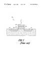
- a field effect transistor 10is formed in a semiconductor 11 by interposing a gate 12 of the transistor between heavily doped regions comprising the source 14 and drain 16 of the transistor as shown in FIG. 1 .
- the gate 12comprised doped polycrystalline silicon (poly) over the gate dielectric 20 .
- the high resistivity of doped polyadversely impacts the switching speed of field effect transistors 10 .
- the gate 12 of a current transistor 10typically comprises a multilayer structure 18 on top of a thin silicon oxide layer 20 in contact with the silicon semiconductor 11 .
- the multilayer structure 18comprises a doped poly layer 22 in contact with the silicon oxide layer 20 and a metallic layer 24 comprising W or WSi 2 in contact with the poly layer 22 .
- a metallic W or WSi 2 layermay be deposited either selectively or nonselectively.
- Moslehi, et al.disclose several selective and nonselective methods for depositing a W layer using a cold wall single wafer thermal/microwave remote plasma multiprocessing reactor.
- selective deposition of W or WSi 2proceeds by the following well known chemical reactions:
- Reactions 1 and 2describe the formation of tungsten. After the tungsten has been formed by either reaction 1 or 2, it can react further with the underlying Si to form WSi 2 (reaction 3). Reaction 4 describes the direct formation of WSi 2 .
- the basic reactionis the silicon (Si) reduction of tungsten hexafluoride (WF 6 ) gas, a displacement reaction where exposed Si is converted to a solid layer of W thereby releasing the displaced Si in the volatile gases SiF 2 and SiF 4 .
- these reactionscause selective deposition of W because only those Si regions exposed to WF 6 on the semiconductor 11 react to form a deposited W layer. There is no conversion to W of regions of the semiconductor 11 having exposed regions comprising materials other than Si, such as silicon oxide (SiO 2 ) or silicon nitride (Si 3 N 4 ).
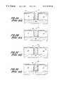
- FIG. 2 aillustrates a cross sectional view of a semiconductor wafer prepared for the substitution of undoped poly by W.
- An oxide layer 32resides on the silicon substrate 30 .
- a barrier layer 34comprising titanium nitride (TiN) resides on the silicon oxide layer 32 and within the contact aperture 38 , where the TiN barrier layer 34 contacts the silicon substrate 30 .
- a conformal poly layer 36is deposited over the TiN barrier layer 34 .
- an etch back of the poly layer 36is performed to remove poly from the TiN barrier layer 34 .
- the etch back stepslightly over etches the poly layer 34 so that the remaining poly 36 is slightly recessed within the aperture 38 .
- a thin chemical oxide layer 40is formed over the poly 36 within the aperture 38 . This chemical oxide layer 40 enhances the subsequent selective deposition of W.
- substitution of poly 36 by W using WF 6 gasoccurs to form a W plug 42 as shown in FIG. 2 d . Note that the entire volume of poly 36 (FIG. 2 c ) within the contact aperture 38 is replaced by W so as to form a W plug 42 .
- the TiN barrier layer 34serves to stop the substitution of Si by W during the selective deposition of a contact. Moreover, this technique is also well adapted to via fills in multilevel metal layer interconnections. However, the TiN barrier layer 34 is not needed in a via fill process as the lower level metal serves to stop the Si substitution by W. Thus, selective deposition of W techniques have found only limited application in contact formation and via fill because of the desire to avoid consumption of exposed Si regions in other device fabrication applications.
- the nonselective WSi 2 depositionresults in deposition of WSi 2 on the reactor walls and other areas exposed to the WF 6 and SiH 4 gas.
- this WSi 2 reactor chamberrequires downtime for frequent etching (cleaning) to remove the WSi 2 buildup on exposed areas.
- microelectronic device manufacturersrequire fabrication methods and systems that enable them to perform multiple processing steps in reactor chambers of substantially similar configuration. Similarly, manufacturers require fabrication methods and systems that enable them to reduce the amount of cleanroom floorspace needed by fabrication equipment. Manufacturers likewise require fabrication methods and systems that reduce the amount of equipment downtime for cleaning and maintenance. In addition, manufacturers require fabrication methods and systems that reduce the need to manage a substantial number of different spares and consumables inventories for multiple different reactors. Moreover, manufacturers require fabrication methods and systems that facilitate continuous improvement of their fabrication equipment by their equipment vendors. Lastly, manufacturers require fabrication methods and systems that reduce the number of multiple different reactors so as to also reduce the amount of capital finds needed to procure fabrication equipment.
- the present inventionenables manufacturers to improve their operations by applying an integrated process to deposit poly or amorphous silicon and tungsten or tungsten silicide for use in the formation of multilayer gate metallizations in semiconductor integrated circuits.
- the present inventioneliminates the need to use different reactors to form poly, tungsten and tungsten silicide layers in a gate structure and reduces the risk of contamination from reactor deposits and incompatible materials.
- the present inventionlikewise reduces equipment downtime for cleaning and maintenance operations associated with deposits on reactor walls and other exposed areas thereby improving equipment throughput.
- the present inventionpermits a manufacturer to form the poly, tungsten and tungsten silicide layers of a gate structure in the same reactor, in another reactor of substantially similar configuration to the reactor used to form the poly layer or in a reaction chamber of a cluster tool of substantially similar configuration to the reactor chamber used to form the poly layer.
- manufacturerscan reduce the costs of procuring a variety of different reactors to form these layers.
- manufacturerscan reduce the cleanroom floorspace occupied by a variety of different reactors to deposit poly, tungsten and tungsten silicide.
- the present inventionreduces the associated costs to manage spares inventories related to a variety of different reactors.
- the present inventionproduces gate metallization structures with improved adhesion between the tungsten or tungsten silicide layers and the poly layer thereby enabling the reduction of gate dimensions to increase circuit densities.
- One aspect of the present inventionincludes a method of forming a gate in a semiconductor integrated circuit comprising the steps of forming a silicon layer over a gate dielectric layer on a substrate and forming a tungsten layer by converting a portion of said silicon layer to tungsten.
- Another aspect of the present inventionincludes a method of forming a gate in a semiconductor integrated circuit device comprising the steps of forming a silicon layer over a gate dielectric layer on a substrate, forming a tungsten layer by converting a portion of said silicon layer to tungsten and annealing said substrate so as to convert a portion of said tungsten layer to a tungsten silicide layer.
- Yet another aspect of the present inventionincludes a method of forming a gate in a semiconductor integrated circuit device comprising the steps of forming a silicon layer over a gate dielectric layer on a substrate and forming a tungsten silicide layer by converting a portion of said silicon layer to tungsten silicide.
- FIG. 1is a cross sectional illustration of a prior art field effect transistor having a multilayer gate structure.
- FIG. 2 ais a cross sectional illustration of a substrate prepared for the formation of a tungsten contact.
- FIG. 2 bis a cross sectional illustration of the substrate of FIG. 2 a after etchback of the polysilicon layer.
- FIG. 2 cis a cross sectional illustration of the substrate of FIG. 2 b after formation of a chemical oxide layer.
- FIG. 2 dis a cross sectional illustration of the substrate of FIG. 2 c after conversion of tungsten to form a tungsten contact (plug).
- FIG. 3is a cross sectional illustration of a substrate prepared for the formation of a gate.
- FIG. 4is a cross sectional illustration of the substrate of FIG. 3 after deposition of a polysilicon layer.
- FIG. 5is a cross sectional illustration of the substrate of FIG. 4 after forming a tungsten layer by conversion of a portion of the polysilicon layer to tungsten.
- FIG. 6is a cross sectional illustration of the substrate of FIG. 5 after removing selected portions of the tungsten and polysilicon layers so as to define a gate.
- FIG. 7is a cross sectional illustration of the substrate of FIG. 5 after sufficient annealing to convert a portion of the tungsten layer to a tungsten silicide layer.
- FIG. 8is a cross sectional illustration of the substrate of FIG. 7 after removing selected portions of the tungsten, tungsten silicide and polysilicon layers so as to define a gate.
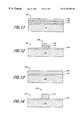
- FIG. 9is a cross sectional illustration of the substrate of FIG. 4 after forming a tungsten layer by conversion of the polysilicon layer to tungsten.
- FIG. 10is a cross sectional illustration of the substrate of FIG. 9 after removing selected portions of the tungsten layer so as to define a gate.
- FIG. 11is a cross sectional illustration of the substrate of FIG. 4 after forming a tungsten silicide layer by conversion of a portion of the polysilicon layer to tungsten silicide.
- FIG. 11also illustrates the substrate of FIG. 5 after sufficient annealing to convert the tungsten layer to a tungsten silicide layer.
- FIG. 12is a cross sectional illustration of the substrate of FIG. 11 after removing selected portions of the tungsten silicide and polysilicon layers so as to define a gate.
- FIG. 13is a cross sectional illustration of the substrate of FIG. 4 after forming a tungsten silicide layer by conversion of the polysilicon layer to tungsten silicide.
- FIG. 14is a cross sectional illustration of the substrate of FIG. 13 after removing selected portions of the tungsten silicide layer so as to define a gate.
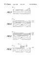
- a substrate 100is prepared for the formation of a gate.
- the term substraterefers to one or more semiconductor layers or structures which include active or operable portions of semiconductor devices.
- a gate dielectric 104has been grown over the entire substrate 100 in preparation for formation of transistor gate structures.
- the substrate 100comprises a silicon semiconductor wafer having a lightly doped single crystal silicon top layer 102 wherein the microelectronic circuits are fabricated.
- the gate dielectric 104comprises a thin layer of silicon oxide having a thickness of about 10 nanometers.
- a silicon layer 112has been deposited over the gate dielectric 104 .
- a polycrystalline silicon (poly) layer 112is formed over the gate dielectric 104 by exposing the substrate 110 to silane (SiH 4 ) gas at a temperature in the range of 575° C. to 800° C. and at a pressure in the range of 0.1 torr to 760 torr for a time sufficient to form a thickness in the range of 100 nanometers to 800 nanometers.
- a poly layer 112is formed over the gate dielectric 104 by exposing the substrate 110 to disilane (Si 2 H 6 ) gas at a temperature in the range of 575° C. to 800° C.
- an amorphous silicon (a-Si) layer 112is formed over the gate dielectric 104 by exposing the substrate 110 to SiH 4 or Si 2 H 6 gas at a temperature in the range of 500° C. to 575° C. and at a pressure in the range of 0.1 torr to 760 torr for a time sufficient to form a thickness in the range of 100 nanometers to 800 nanometers.
- the a-Si layer formedmay include some polycrystalline silicon regions. Note that deposited a-Si layers often have smoother surfaces and better uniformity as compared to deposited poly layers.
- the silicon layer 112may be doped in situ during its formation.
- dopant gasessuch as AsH 3 , PH 3 and B 2 H 6 , are added to the SiH 4 or Si 2 H 6 flow during formation of the poly or a-Si layer.
- the dopant profiles within the silicon layer 112may be defined by adjustment of the dopant gas flowrate during formation of the silicon layer 112 . For example, if the dopant gas flow is shut off prior to that for the SiH 4 , the top portion of the silicon layer 112 will be undoped while the bottom portion is doped.
- the top portion of the silicon layer 112will be more heavily doped than the bottom portion.
- the ability to fabricate a silicon layer 112 having a tailored dopant concentration profilefacilitates subsequent device processing.
- a tungsten layeris formed from a portion of the poly layer 112 using the displacement reaction.
- formation of a tungsten layer 124proceeds by exposing the poly layer 112 (FIG. 4) of the substrate 110 (FIG. 4) to tungsten hexafluoride (WF 6 ) gas at a temperature in the range of 300° C. to 400° C. and at a pressure in the range of 0.1 to 760 torr.
- WF 6tungsten hexafluoride
- the WF 6will be diluted in a carrier gas, such as argon (Ar) or nitrogen (N 2 ).
- any gasmay be selected as a carrier gas so long as the carrier gas does not react with WF 6 to deposit W on top of the poly layer 112 instead of converting a portion of the poly layer 112 to form a tungsten layer 124 .
- a tungsten layer 124 of a selected self-limiting thicknessis formed over the poly layer 122 .
- Self-limitingrefers to a condition where the growth of the tungsten layer 124 stops after a certain time, even though sufficient quantities of WF 6 are still available for reaction with Si.
- a self-limiting tungsten film of about 20 nmis formed in approximately 10 seconds.
- the growth of the tungsten layer 124is maintained by Si diffusion from the poly layer 122 until the reaction abruptly stops due to the self-limiting effect.
- the reaction rateis determined by the WF 6 gas diffusion through a boundary layer that forms above the top surface of the tungsten layer 124 in the gas phase.
- the growth rate of the tungsten layer 124is proportional to the WF 6 pressure and inversely proportional to the total pressure.
- the self-limiting effectoccurs when the reaction rate becomes limited by the supply of Si atoms from the poly layer 122 to the top surface of the tungsten layer 124 . At this moment, the fast diffusion paths for Si are blocked rapidly and the growth stops. As the diffusion of Si to the top surface of the tungsten layer 124 is thermally activated, the thickness of the tungsten layer 124 can be engineered by selecting the proper temperature, WF 6 and total pressure. In another preferred embodiment, the formation of a tungsten layer 124 occurs in the same reactor used to form the poly layer 112 (FIG. 4 ). In yet another preferred embodiment, the formation of a tungsten layer 124 occurs in another reactor of substantially similar configuration to the reactor used to form the poly layer 112 (FIG. 4 ).
- formation of a tungsten layer 124occurs in a reaction chamber of a cluster tool of substantially similar configuration to the reactor chamber used to form the poly layer 112 (FIG. 4 ).
- a multilayer gate structure 136is subsequently defined by removing selected portions of the poly layer 122 and the tungsten layer 124 as shown in FIG. 6 . Note that the gate 136 includes a tungsten layer 134 over a poly layer 132 .
- a tungsten silicide layermay be formed by conversion of a portion of the remaining poly layer 112 .
- a portion of the tungsten layer 124 (FIG. 5)has been converted to a tungsten silicide layer 146 by annealing the substrate 120 (FIG. 5) under an inert atmosphere, such as Argon, at a temperature in the range of 600° C. to 1000° C. to form a tungsten silicide layer 146 .
- the substrate 120FIG.
- the substrate 120 (FIG. 5)is annealed in the same reactor used to form the poly layer 112 (FIG. 4) and to form the tungsten layer 124 (FIG. 5 ).
- the substrate 120 (FIG. 5)is annealed in another reactor of substantially similar configuration to the reactor used to form the poly layer 112 (FIG. 4) and to form the tungsten layer 124 (FIG. 5 ).
- the substrate 120 (FIG. 5)is annealed in a reaction chamber of a cluster tool of substantially similar configuration to the reactor chamber used to form the poly layer 112 (FIG. 4) and to form the tungsten layer 124 (FIG. 5 ).
- a multilayer gate structure 158is subsequently defined by removing selected portions of the poly layer 142 , the tungsten silicide layer 146 and the tungsten layer 144 as shown in FIG. 8 .
- the gate 158includes a tungsten layer 154 over a tungsten silicide layer 156 over a poly layer 152 .
- the entire poly layer 112(FIG. 4) is converted into a tungsten layer 162 by using either a higher total pressure, a lower WF 6 partial pressure or a higher temperature. Under these conditions, all of the poly layer 112 is consumed before the self-limiting thickness is reached.
- formation of a tungsten layer 162proceeds by exposing the poly layer 112 (FIG. 4) of the substrate 110 (FIG. 4) to tungsten hexafluoride (WF 6 ) gas at a temperature in the range of 300° C. to 400° C. and at a total pressure in the range of 0.1 to 760 torr for a time sufficient to convert the entire poly layer 112 (FIG.
- tungstenFor example, at a temperature of 370° C., a total pressure of 4.0 torr, a WF 6 flow of 50 sccm and an Ar flow of 2000 sccm, a 300 nm poly layer is entirely consumed to form a tungsten film of about 150 nm thickness in approximately 160 seconds. As noted above, there is no self-limiting effect here because the entire poly layer 112 (FIG. 4 ) is already consumed before the self-limiting thickness is reached.
- a 300 nm poly layeris entirely consumed to form a tungsten film of about 150 nm thickness in approximately 180 seconds.
- formation of a tungsten layer 162proceeds by exposing the poly layer 112 (FIG. 4) of the substrate 110 (FIG. 4) to tungsten hexafluoride (WF 6 ) gas at a temperature in the range of 300° C. to 400° C.
- a WF 6 partial pressurein the range of 0.0025 torr to 76 torr for a time sufficient convert the entire poly layer 112 (FIG. 4) to tungsten.
- a temperature of 370° C.a total pressure of 0.5 torr, a WF 6 flow of 12.5 sccm and an Ar flow of 2000 sccm, a 300 nm poly layer is entirely consumed to form a tungsten film of about 150 nm thickness in approximately 160 seconds.
- formation of a tungsten layer 162occurs in the same reactor used to form the poly layer 112 (FIG. 4 ).
- formation of a tungsten layer 162occurs in another reactor of substantially similar configuration to the reactor used to form the poly layer 112 (FIG. 4 ). In yet another preferred embodiment, formation of a tungsten layer 162 occurs in a reaction chamber of a cluster tool of substantially similar configuration to the reactor chamber used to form the poly layer 112 (FIG. 4 ). A tungsten gate structure 174 is subsequently defined by removing selected portions of the tungsten layer 162 as shown in the substrate 170 in FIG. 10 .
- a tungsten silicide layermay also be formed from a portion of the poly layer 112 (FIG. 4 ).
- formation of a tungsten silicide layer 184proceeds by exposing the poly layer 112 (FIG. 4) of the substrate 110 (FIG. 4) to tungsten hexafluoride (WF 6 ) gas at temperatures generally above 450° C. and at a pressure in the range of 0.1 to 760 torr. Under these conditions, the self limiting effect does not occur.
- WF 6tungsten hexafluoride
- a WSi 2 layer of 145 nm thicknessis formed when the WF 6 flow is terminated in approximately 50 seconds.
- the tungsten silicide layer 184 formedmay be in the metastable hexagonal high resistivity phase.
- the substrate 180is annealed under an inert atmosphere, such as Argon, at a temperature in the range of 600° C. to 1000° C. for a time sufficient to convert the entire hexagonal tungsten silicide phase to the lower resistivity tetragonal tungsten silicide phase.
- formation of a tungsten silicide layer 184occurs in the same reactor used to form the poly layer 112 (FIG. 4 ). In yet another preferred embodiment, formation of a tungsten silicide layer 184 occurs in another reactor of substantially similar configuration to the reactor used to form the poly layer 112 (FIG. 4 ). In yet another preferred embodiment, formation of a tungsten silicide layer 184 occurs in a reaction chamber of a cluster tool of substantially similar configuration to the reactor chamber used to form the poly layer 112 (FIG. 4 ).
- FIG. 11also illustrates the substrate 120 (FIG. 5) after sufficient annealing to convert the tungsten layer 124 (FIG. 5) and a portion of the poly layer 122 (FIG. 5) to a tungsten silicide layer 184 .
- the substrate 120 (FIG. 5) having a tungsten layer 124 over a poly layer 122 (FIG. 5)is annealed under an inert atmosphere, such as Argon, at a temperature in the range of 600° C. to 1000° C. for a time sufficient to convert the entire tungsten layer 124 (FIG. 5) to tungsten silicide 184 .
- the substrate 120 (FIG. 5)is annealed under an inert atmosphere, such as Argon, at a temperature in the range of 600° C. to 1000° C. for a time sufficient to convert the entire tungsten layer 124 (FIG. 5) to tungsten silicide 184 .
- the substrate 120 (FIG. 5)is
- the substrate 120 (FIG. 5)is annealed in the same reactor used to form the poly layer 112 (FIG. 4) and to form the tungsten layer 124 (FIG. 5 ).
- the substrate 120 (FIG. 5)is annealed in another reactor of substantially similar configuration to the reactor used to form the poly layer 112 (FIG. 4) and to form the tungsten layer 124 (FIG. 5 ).
- the substrate 120 (FIG. 5)is annealed in a reaction chamber of a cluster tool of substantially similar configuration to the reactor chamber used to form the poly layer 112 (FIG. 4) and to form the tungsten layer 124 (FIG. 5 ).
- a multilayer gate structure 196is subsequently defined by removing selected portions of the poly layer 182 and the tungsten silicide layer 184 as shown in the substrate 190 in FIG. 12 . Note that the gate 196 includes a tungsten silicide layer 194 over a poly layer 192 .
- the entire poly layer 112(FIG. 4) is converted into a tungsten silicide layer 202 .
- formation of a tungsten silicide layer 202proceeds by exposing the poly layer 112 (FIG. 4) of the substrate 110 (FIG. 4) to tungsten hexafluoride (WF 6 ) gas at temperatures generally above 450° C. and at a pressure in the range of 0.1 to 760 torr until the entire poly layer 112 (FIG. 4) has been consumed.
- WF 6tungsten hexafluoride
- a 450 nm poly layeris entirely consumed to form a tungsten silicide film of about 250 nm thickness in approximately 250 seconds.
- the tungsten silicide layer 202 formedmay be in the metastable hexagonal high resistivity phase.
- the substrate 180is annealed under an inert atmosphere, such as Argon, at a temperature in the range of 600° C. to 1000° C. for a time sufficient to convert the entire hexagonal tungsten silicide phase to the lower resistivity tetragonal tungsten silicide phase.
- formation of a tungsten silicide layer 202occurs in the same reactor used to form the poly layer 112 (FIG. 4 ). In yet another preferred embodiment, formation of a tungsten silicide layer 202 occurs in another reactor of substantially similar configuration to the reactor used to form the poly layer 112 (FIG. 4 ). In yet another preferred embodiment, formation of a tungsten silicide layer 202 occurs in a reaction chamber of a cluster tool of substantially similar configuration to the reactor chamber used to form the poly layer 112 (FIG. 4 ). A tungsten silicide gate structure 214 is subsequently defined by removing selected portions of the tungsten silicide layer 202 to leave a patterned tungsten silicide layer 212 as shown in FIG. 14 .
- the present inventionadvantageously overcomes several limitations of existing technologies and alternatives.
- a reducing agentsuch as H 2 or SiH 4 is added to the WF 6 flow
- the WF 6 Si conversion reactionproduces no deposits or coatings on the reactor walls.
- a semiconductor device manufacturer using the present invention to form gate metallizationsavoids contamination from reactor coatings and deposits.
- the manufacturercan improve the throughput of its reactors by avoiding frequent reactor cleans required for present deposition methods.
- use of the present invention to form a multilayer gate structureproduces improved adhesion between the tungsten or tungsten silicide layers and the poly layer as compared to the adhesion of a traditionally deposited tungsten silicide layer on the poly layer, which exhibit cracking followed by delamination with narrower gate dimensions.
- the present inventioneliminates the need to use different reactors to form the poly layer and the tungsten or tungsten silicide layer.
- a manufacturercan form a poly layer followed by a tungsten or tungsten silicide layer in the same reactor, in another reactor of substantially similar configuration to the reactor used to form the poly layer or in a reaction chamber of a cluster tool of substantially similar configuration to the reactor chamber used to form the poly layer.
- This flexibilityallows the manufacturer to save costs related to the procurement, installation, use and maintenance of multiple different reactors.
- a manufacturerthus realizes certain economies of scale as reactors share the same parts, require the same maintenance and the same training to operate.
- the present inventionenables the metallization of a full batch of poly deposited wafers at once with tungsten or tungsten silicide.
Landscapes
- Engineering & Computer Science (AREA)
- General Physics & Mathematics (AREA)
- Physics & Mathematics (AREA)
- Condensed Matter Physics & Semiconductors (AREA)
- Manufacturing & Machinery (AREA)
- Computer Hardware Design (AREA)
- Microelectronics & Electronic Packaging (AREA)
- Power Engineering (AREA)
- Chemical Kinetics & Catalysis (AREA)
- Chemical & Material Sciences (AREA)
- General Chemical & Material Sciences (AREA)
- Insulated Gate Type Field-Effect Transistor (AREA)
- Electrodes Of Semiconductors (AREA)
Abstract
Description
1. Field of the Invention
The present invention relates to microelectronic device fabrication, and more particularly, to a method of forming tungsten or tungsten silicide layers for use in gate metallizations and local interconnects in a semiconductor integrated circuit.
2. Description of the Related Technology
In microelectronic devices common in the art, afield effect transistor 10 is formed in a semiconductor11 by interposing agate 12 of the transistor between heavily doped regions comprising thesource 14 anddrain 16 of the transistor as shown in FIG.1. In older semiconductor devices, thegate 12 comprised doped polycrystalline silicon (poly) over the gate dielectric20. However, as the dimensions of transistors and their interconnections have decreased into the submicron region, the high resistivity of doped poly adversely impacts the switching speed offield effect transistors 10. Thus, to increase the switching speed of atransistor 10, semiconductor manufacturers use amultilayer structure 18 including a metallic layer, such as tungsten (W) or tungsten silicide (WSi2), to reduce the resistivity ofgates 12 and local interconnect lines so as to increase the operating speed of circuits formed from interconnected transistors. Thus, thegate 12 of acurrent transistor 10 typically comprises amultilayer structure 18 on top of a thinsilicon oxide layer 20 in contact with the silicon semiconductor11. Themultilayer structure 18 comprises a dopedpoly layer 22 in contact with thesilicon oxide layer 20 and ametallic layer 24 comprising W or WSi2in contact with thepoly layer 22.
During the formation of the microelectronic device, a metallic W or WSi2layer may be deposited either selectively or nonselectively. In U.S. Pat. No. 4,913,929, Moslehi, et al., disclose several selective and nonselective methods for depositing a W layer using a cold wall single wafer thermal/microwave remote plasma multiprocessing reactor. Moreover, as described by Leusink, et al., inJ. Appl. Phys.72, 490 (1992), selective deposition of W or WSi2proceeds by the following well known chemical reactions:
Reactions 1 and 2 describe the formation of tungsten. After the tungsten has been formed by either reaction 1 or 2, it can react further with the underlying Si to form WSi2(reaction 3). Reaction 4 describes the direct formation of WSi2. Thus, the basic reaction is the silicon (Si) reduction of tungsten hexafluoride (WF6) gas, a displacement reaction where exposed Si is converted to a solid layer of W thereby releasing the displaced Si in the volatile gases SiF2and SiF4. In contrast to nonselective or blanket depositions, these reactions cause selective deposition of W because only those Si regions exposed to WF6on the semiconductor11 react to form a deposited W layer. There is no conversion to W of regions of the semiconductor11 having exposed regions comprising materials other than Si, such as silicon oxide (SiO2) or silicon nitride (Si3N4).
According to reactions (1) and (2), every nanometer of W formed consumes approximately two nanometers of the exposed Si. Thus, as noted by Leusink, et al., the Si reduction of WF6should be suppressed as the etching of exposed Si, such as source or drain regions, is an undesired result. To prevent or reduce undesired etching of exposed Si regions, combinations of WF6gas and reducing agents, such as the gases H2, SiH4or GeH4, have been used for the chemical vapor deposition (CVD) of W. Currently, tungsten CVD by WF6/H2or WF6/SiH4are the preferred methods used in the microelectronics industry. However, inIEEE Trans. Electron Devices, 37, 577 (1990), Kobayashi, et al., describe applying the selective deposition of W to form a W contact (plug) by substitution of undoped poly by W. FIG. 2aillustrates a cross sectional view of a semiconductor wafer prepared for the substitution of undoped poly by W. Anoxide layer 32 resides on thesilicon substrate 30. Abarrier layer 34 comprising titanium nitride (TiN) resides on thesilicon oxide layer 32 and within thecontact aperture 38, where theTiN barrier layer 34 contacts thesilicon substrate 30. Lastly, aconformal poly layer 36 is deposited over theTiN barrier layer 34.
Referring now to FIG. 2b, an etch back of thepoly layer 36 is performed to remove poly from theTiN barrier layer 34. Note that the etch back step slightly over etches thepoly layer 34 so that theremaining poly 36 is slightly recessed within theaperture 38. Referring now to FIG. 2c, a thinchemical oxide layer 40 is formed over thepoly 36 within theaperture 38. Thischemical oxide layer 40 enhances the subsequent selective deposition of W. Lastly, substitution ofpoly 36 by W using WF6gas occurs to form aW plug 42 as shown in FIG. 2d. Note that the entire volume of poly36 (FIG. 2c) within thecontact aperture 38 is replaced by W so as to form aW plug 42. TheTiN barrier layer 34 serves to stop the substitution of Si by W during the selective deposition of a contact. Moreover, this technique is also well adapted to via fills in multilevel metal layer interconnections. However, theTiN barrier layer 34 is not needed in a via fill process as the lower level metal serves to stop the Si substitution by W. Thus, selective deposition of W techniques have found only limited application in contact formation and via fill because of the desire to avoid consumption of exposed Si regions in other device fabrication applications.
Although Moslehi, et al., disclose in U.S. Pat. No. 4,913,929 that several wafer processing steps can be done sequentially in a single reactor, semiconductor manufacturers currently use multiple reactors of significantly different configuration to form and interconnect the many layers needed in a microelectronic device. For example, a manufacturer may use a cluster tool, such as an Applied Materials Centura, having a reactor chamber dedicated to the deposition of poly and also having a reactor chamber of significantly different configuration dedicated to the deposition of WSi2. The present art for tungsten silicide formation uses a gas mixture consisting of tungsten hexafluoride and silane or dichlorosilane. The tungsten silicide deposits according to the following reactions:
The nonselective WSi2deposition results in deposition of WSi2on the reactor walls and other areas exposed to the WF6and SiH4gas. Thus, this WSi2reactor chamber requires downtime for frequent etching (cleaning) to remove the WSi2buildup on exposed areas.
The use of multiple different reactors often results from a strategy to prevent incompatible chemical reactions and materials produced during the formation of a prior layer from impacting the formation of a current or subsequent layer in the same reactor. This strategy is of critical importance to a semiconductor manufacturer as minuscule amounts of impurities in any single layer of a microelectronic device often result in device failures and scrap. At the same time, however, the need for multiple reactors of different configuration creates substantial operational issues in addition to the significant capital funds required to procure multiple different reactors. For example, the manufacturer has to maintain spares for each of the multiple reactor configurations used in its factory at a considerable cost for spares inventory, warehousing and personnel to manage spares.
To improve their operations, microelectronic device manufacturers require fabrication methods and systems that enable them to perform multiple processing steps in reactor chambers of substantially similar configuration. Similarly, manufacturers require fabrication methods and systems that enable them to reduce the amount of cleanroom floorspace needed by fabrication equipment. Manufacturers likewise require fabrication methods and systems that reduce the amount of equipment downtime for cleaning and maintenance. In addition, manufacturers require fabrication methods and systems that reduce the need to manage a substantial number of different spares and consumables inventories for multiple different reactors. Moreover, manufacturers require fabrication methods and systems that facilitate continuous improvement of their fabrication equipment by their equipment vendors. Lastly, manufacturers require fabrication methods and systems that reduce the number of multiple different reactors so as to also reduce the amount of capital finds needed to procure fabrication equipment.
The present invention enables manufacturers to improve their operations by applying an integrated process to deposit poly or amorphous silicon and tungsten or tungsten silicide for use in the formation of multilayer gate metallizations in semiconductor integrated circuits. In contrast to present methods that produce tungsten or tungsten silicide deposits on reactor walls and other exposed areas, the present invention eliminates the need to use different reactors to form poly, tungsten and tungsten silicide layers in a gate structure and reduces the risk of contamination from reactor deposits and incompatible materials. The present invention likewise reduces equipment downtime for cleaning and maintenance operations associated with deposits on reactor walls and other exposed areas thereby improving equipment throughput. Moreover, the present invention permits a manufacturer to form the poly, tungsten and tungsten silicide layers of a gate structure in the same reactor, in another reactor of substantially similar configuration to the reactor used to form the poly layer or in a reaction chamber of a cluster tool of substantially similar configuration to the reactor chamber used to form the poly layer. Thus, using the present invention, manufacturers can reduce the costs of procuring a variety of different reactors to form these layers. Similarly, manufacturers can reduce the cleanroom floorspace occupied by a variety of different reactors to deposit poly, tungsten and tungsten silicide. In addition, the present invention reduces the associated costs to manage spares inventories related to a variety of different reactors. Lastly, in contrast to structures fabricated using conventional techniques, the present invention produces gate metallization structures with improved adhesion between the tungsten or tungsten silicide layers and the poly layer thereby enabling the reduction of gate dimensions to increase circuit densities.
One aspect of the present invention includes a method of forming a gate in a semiconductor integrated circuit comprising the steps of forming a silicon layer over a gate dielectric layer on a substrate and forming a tungsten layer by converting a portion of said silicon layer to tungsten.
Another aspect of the present invention includes a method of forming a gate in a semiconductor integrated circuit device comprising the steps of forming a silicon layer over a gate dielectric layer on a substrate, forming a tungsten layer by converting a portion of said silicon layer to tungsten and annealing said substrate so as to convert a portion of said tungsten layer to a tungsten silicide layer.
Yet another aspect of the present invention includes a method of forming a gate in a semiconductor integrated circuit device comprising the steps of forming a silicon layer over a gate dielectric layer on a substrate and forming a tungsten silicide layer by converting a portion of said silicon layer to tungsten silicide.
FIG. 1 is a cross sectional illustration of a prior art field effect transistor having a multilayer gate structure.
FIG. 2ais a cross sectional illustration of a substrate prepared for the formation of a tungsten contact.
FIG. 2bis a cross sectional illustration of the substrate of FIG. 2aafter etchback of the polysilicon layer.
FIG. 2cis a cross sectional illustration of the substrate of FIG. 2bafter formation of a chemical oxide layer.
FIG. 2dis a cross sectional illustration of the substrate of FIG. 2cafter conversion of tungsten to form a tungsten contact (plug).
FIG. 3 is a cross sectional illustration of a substrate prepared for the formation of a gate.
FIG. 4 is a cross sectional illustration of the substrate of FIG. 3 after deposition of a polysilicon layer.
FIG. 5 is a cross sectional illustration of the substrate of FIG. 4 after forming a tungsten layer by conversion of a portion of the polysilicon layer to tungsten.
FIG. 6 is a cross sectional illustration of the substrate of FIG. 5 after removing selected portions of the tungsten and polysilicon layers so as to define a gate.
FIG. 7 is a cross sectional illustration of the substrate of FIG. 5 after sufficient annealing to convert a portion of the tungsten layer to a tungsten silicide layer.
FIG. 8 is a cross sectional illustration of the substrate of FIG. 7 after removing selected portions of the tungsten, tungsten silicide and polysilicon layers so as to define a gate.
FIG. 9 is a cross sectional illustration of the substrate of FIG. 4 after forming a tungsten layer by conversion of the polysilicon layer to tungsten.
FIG. 10 is a cross sectional illustration of the substrate of FIG. 9 after removing selected portions of the tungsten layer so as to define a gate.
FIG. 11 is a cross sectional illustration of the substrate of FIG. 4 after forming a tungsten silicide layer by conversion of a portion of the polysilicon layer to tungsten silicide. FIG. 11 also illustrates the substrate of FIG. 5 after sufficient annealing to convert the tungsten layer to a tungsten silicide layer.
FIG. 12 is a cross sectional illustration of the substrate of FIG. 11 after removing selected portions of the tungsten silicide and polysilicon layers so as to define a gate.
FIG. 13 is a cross sectional illustration of the substrate of FIG. 4 after forming a tungsten silicide layer by conversion of the polysilicon layer to tungsten silicide.
FIG. 14 is a cross sectional illustration of the substrate of FIG. 13 after removing selected portions of the tungsten silicide layer so as to define a gate.
Referring now to FIG. 3, asubstrate 100 is prepared for the formation of a gate. The term substrate refers to one or more semiconductor layers or structures which include active or operable portions of semiconductor devices. Agate dielectric 104 has been grown over theentire substrate 100 in preparation for formation of transistor gate structures. In a preferred embodiment, thesubstrate 100 comprises a silicon semiconductor wafer having a lightly doped single crystalsilicon top layer 102 wherein the microelectronic circuits are fabricated. Thegate dielectric 104 comprises a thin layer of silicon oxide having a thickness of about 10 nanometers.
Referring now to FIG. 4, asilicon layer 112 has been deposited over thegate dielectric 104. In a preferred embodiment, a polycrystalline silicon (poly)layer 112 is formed over thegate dielectric 104 by exposing thesubstrate 110 to silane (SiH4) gas at a temperature in the range of 575° C. to 800° C. and at a pressure in the range of 0.1 torr to 760 torr for a time sufficient to form a thickness in the range of 100 nanometers to 800 nanometers. In another preferred embodiment, apoly layer 112 is formed over thegate dielectric 104 by exposing thesubstrate 110 to disilane (Si2H6) gas at a temperature in the range of 575° C. to 800° C. and at a pressure in the range of 0.1 torr to 760 torr for a time sufficient to form a thickness in the range of 100 nanometers to 800 nanometers. Generally, the SiH4and Si2H6flows will be diluted in a H2or N2carrier gas. In yet another preferred embodiment, an amorphous silicon (a-Si)layer 112 is formed over thegate dielectric 104 by exposing thesubstrate 110 to SiH4or Si2H6gas at a temperature in the range of 500° C. to 575° C. and at a pressure in the range of 0.1 torr to 760 torr for a time sufficient to form a thickness in the range of 100 nanometers to 800 nanometers. In the higher temperature range, the a-Si layer formed may include some polycrystalline silicon regions. Note that deposited a-Si layers often have smoother surfaces and better uniformity as compared to deposited poly layers.
Moreover, thesilicon layer 112 may be doped in situ during its formation. In a preferred embodiment, dopant gases, such as AsH3, PH3and B2H6, are added to the SiH4or Si2H6flow during formation of the poly or a-Si layer. The dopant profiles within thesilicon layer 112 may be defined by adjustment of the dopant gas flowrate during formation of thesilicon layer 112. For example, if the dopant gas flow is shut off prior to that for the SiH4, the top portion of thesilicon layer 112 will be undoped while the bottom portion is doped. Similarly, if the dopant gas flow is increased towards the end of the deposition process, the top portion of thesilicon layer 112 will be more heavily doped than the bottom portion. The ability to fabricate asilicon layer 112 having a tailored dopant concentration profile facilitates subsequent device processing.
After depositing thepoly layer 112, a tungsten layer is formed from a portion of thepoly layer 112 using the displacement reaction. Referring now to FIG. 5, in a preferred embodiment, formation of atungsten layer 124 proceeds by exposing the poly layer112 (FIG. 4) of the substrate110 (FIG. 4) to tungsten hexafluoride (WF6) gas at a temperature in the range of 300° C. to 400° C. and at a pressure in the range of 0.1 to 760 torr. Generally, the WF6will be diluted in a carrier gas, such as argon (Ar) or nitrogen (N2). Note that any gas may be selected as a carrier gas so long as the carrier gas does not react with WF6to deposit W on top of thepoly layer 112 instead of converting a portion of thepoly layer 112 to form atungsten layer 124. Under these conditions, atungsten layer 124 of a selected self-limiting thickness is formed over the poly layer122. Self-limiting refers to a condition where the growth of thetungsten layer 124 stops after a certain time, even though sufficient quantities of WF6are still available for reaction with Si. For example, at a temperature of 370° C., a total pressure of 0.5 torr, a WF6flow of 50 sccm and an Ar flow of 2000 sccm, a self-limiting tungsten film of about 20 nm is formed in approximately 10 seconds. Note that the growth of thetungsten layer 124 is maintained by Si diffusion from the poly layer122 until the reaction abruptly stops due to the self-limiting effect. At temperatures above about 300° C., the reaction rate is determined by the WF6gas diffusion through a boundary layer that forms above the top surface of thetungsten layer 124 in the gas phase. Thus, the growth rate of thetungsten layer 124 is proportional to the WF6pressure and inversely proportional to the total pressure. The self-limiting effect occurs when the reaction rate becomes limited by the supply of Si atoms from the poly layer122 to the top surface of thetungsten layer 124. At this moment, the fast diffusion paths for Si are blocked rapidly and the growth stops. As the diffusion of Si to the top surface of thetungsten layer 124 is thermally activated, the thickness of thetungsten layer 124 can be engineered by selecting the proper temperature, WF6and total pressure. In another preferred embodiment, the formation of atungsten layer 124 occurs in the same reactor used to form the poly layer112 (FIG.4). In yet another preferred embodiment, the formation of atungsten layer 124 occurs in another reactor of substantially similar configuration to the reactor used to form the poly layer112 (FIG.4). In yet another preferred embodiment, formation of atungsten layer 124 occurs in a reaction chamber of a cluster tool of substantially similar configuration to the reactor chamber used to form the poly layer112 (FIG.4). Amultilayer gate structure 136 is subsequently defined by removing selected portions of the poly layer122 and thetungsten layer 124 as shown in FIG.6. Note that thegate 136 includes atungsten layer 134 over apoly layer 132.
Once a tungsten layer124 (FIG. 5) has been formed from a portion of the poly layer112 (FIG.4), a tungsten silicide layer may be formed by conversion of a portion of the remainingpoly layer 112. Referring now to FIG. 7, in a preferred embodiment, a portion of the tungsten layer124 (FIG. 5) has been converted to atungsten silicide layer 146 by annealing the substrate120 (FIG. 5) under an inert atmosphere, such as Argon, at a temperature in the range of 600° C. to 1000° C. to form atungsten silicide layer 146. In another preferred embodiment, the substrate120 (FIG. 5) is annealed in the same reactor used to form the poly layer112 (FIG. 4) and to form the tungsten layer124 (FIG.5). In yet another preferred embodiment, the substrate120 (FIG. 5) is annealed in another reactor of substantially similar configuration to the reactor used to form the poly layer112 (FIG. 4) and to form the tungsten layer124 (FIG.5). In yet another preferred embodiment, the substrate120 (FIG. 5) is annealed in a reaction chamber of a cluster tool of substantially similar configuration to the reactor chamber used to form the poly layer112 (FIG. 4) and to form the tungsten layer124 (FIG.5). Amultilayer gate structure 158 is subsequently defined by removing selected portions of thepoly layer 142, thetungsten silicide layer 146 and the tungsten layer144 as shown in FIG.8. Note that thegate 158 includes atungsten layer 154 over atungsten silicide layer 156 over apoly layer 152.
Referring now to FIG. 9, the entire poly layer112 (FIG. 4) is converted into atungsten layer 162 by using either a higher total pressure, a lower WF6partial pressure or a higher temperature. Under these conditions, all of thepoly layer 112 is consumed before the self-limiting thickness is reached. In a preferred embodiment, formation of atungsten layer 162 proceeds by exposing the poly layer112 (FIG. 4) of the substrate110 (FIG. 4) to tungsten hexafluoride (WF6) gas at a temperature in the range of 300° C. to 400° C. and at a total pressure in the range of 0.1 to 760 torr for a time sufficient to convert the entire poly layer112 (FIG. 4) to tungsten. For example, at a temperature of 370° C., a total pressure of 4.0 torr, a WF6flow of 50 sccm and an Ar flow of 2000 sccm, a 300 nm poly layer is entirely consumed to form a tungsten film of about 150 nm thickness in approximately 160 seconds. As noted above, there is no self-limiting effect here because the entire poly layer112 (FIG.4) is already consumed before the self-limiting thickness is reached. For example, at a temperature of 400° C., a total pressure of 0.5 torr, a WF6flow of 25 sccm and an Ar flow of 2000 sccm, a 300 nm poly layer is entirely consumed to form a tungsten film of about 150 nm thickness in approximately 180 seconds. In yet another preferred embodiment, formation of atungsten layer 162 proceeds by exposing the poly layer112 (FIG. 4) of the substrate110 (FIG. 4) to tungsten hexafluoride (WF6) gas at a temperature in the range of 300° C. to 400° C. and at a WF6partial pressure in the range of 0.0025 torr to 76 torr for a time sufficient convert the entire poly layer112 (FIG. 4) to tungsten. For example, at a temperature of 370° C., a total pressure of 0.5 torr, a WF6flow of 12.5 sccm and an Ar flow of 2000 sccm, a 300 nm poly layer is entirely consumed to form a tungsten film of about 150 nm thickness in approximately 160 seconds. In yet another preferred embodiment, formation of atungsten layer 162 occurs in the same reactor used to form the poly layer112 (FIG.4). In yet another preferred embodiment, formation of atungsten layer 162 occurs in another reactor of substantially similar configuration to the reactor used to form the poly layer112 (FIG.4). In yet another preferred embodiment, formation of atungsten layer 162 occurs in a reaction chamber of a cluster tool of substantially similar configuration to the reactor chamber used to form the poly layer112 (FIG.4). Atungsten gate structure 174 is subsequently defined by removing selected portions of thetungsten layer 162 as shown in thesubstrate 170 in FIG.10.
Moreover, a tungsten silicide layer may also be formed from a portion of the poly layer112 (FIG.4). Referring now to FIG. 11, in a preferred embodiment, formation of atungsten silicide layer 184 proceeds by exposing the poly layer112 (FIG. 4) of the substrate110 (FIG. 4) to tungsten hexafluoride (WF6) gas at temperatures generally above 450° C. and at a pressure in the range of 0.1 to 760 torr. Under these conditions, the self limiting effect does not occur. Thus, to form atungsten silicide layer 184 of a predetermined thickness over thepoly layer 182, the WF6flow must be terminated. For example, at a temperature of 500° C., a total pressure of 0.5 torr, a WF6flow of 10 sccm and an Ar flow of 2000 sccm, a WSi2layer of 145 nm thickness is formed when the WF6flow is terminated in approximately 50 seconds. Note that thetungsten silicide layer 184 formed may be in the metastable hexagonal high resistivity phase. To reduce the resistivity, thesubstrate 180 is annealed under an inert atmosphere, such as Argon, at a temperature in the range of 600° C. to 1000° C. for a time sufficient to convert the entire hexagonal tungsten silicide phase to the lower resistivity tetragonal tungsten silicide phase. In another preferred embodiment, formation of atungsten silicide layer 184 occurs in the same reactor used to form the poly layer112 (FIG.4). In yet another preferred embodiment, formation of atungsten silicide layer 184 occurs in another reactor of substantially similar configuration to the reactor used to form the poly layer112 (FIG.4). In yet another preferred embodiment, formation of atungsten silicide layer 184 occurs in a reaction chamber of a cluster tool of substantially similar configuration to the reactor chamber used to form the poly layer112 (FIG.4).
FIG. 11 also illustrates the substrate120 (FIG. 5) after sufficient annealing to convert the tungsten layer124 (FIG. 5) and a portion of the poly layer122 (FIG. 5) to atungsten silicide layer 184. In a preferred embodiment, the substrate120 (FIG. 5) having atungsten layer 124 over a poly layer122 (FIG. 5) is annealed under an inert atmosphere, such as Argon, at a temperature in the range of 600° C. to 1000° C. for a time sufficient to convert the entire tungsten layer124 (FIG. 5) totungsten silicide 184. In another preferred embodiment, the substrate120 (FIG. 5) is annealed in the same reactor used to form the poly layer112 (FIG. 4) and to form the tungsten layer124 (FIG.5). In yet another preferred embodiment, the substrate120 (FIG. 5) is annealed in another reactor of substantially similar configuration to the reactor used to form the poly layer112 (FIG. 4) and to form the tungsten layer124 (FIG.5). In yet another preferred embodiment, the substrate120 (FIG. 5) is annealed in a reaction chamber of a cluster tool of substantially similar configuration to the reactor chamber used to form the poly layer112 (FIG. 4) and to form the tungsten layer124 (FIG.5). Amultilayer gate structure 196 is subsequently defined by removing selected portions of thepoly layer 182 and thetungsten silicide layer 184 as shown in thesubstrate 190 in FIG.12. Note that thegate 196 includes atungsten silicide layer 194 over apoly layer 192.
Referring now to FIG. 13, the entire poly layer112 (FIG. 4) is converted into atungsten silicide layer 202. In a preferred embodiment, formation of atungsten silicide layer 202 proceeds by exposing the poly layer112 (FIG. 4) of the substrate110 (FIG. 4) to tungsten hexafluoride (WF6) gas at temperatures generally above 450° C. and at a pressure in the range of 0.1 to 760 torr until the entire poly layer112 (FIG. 4) has been consumed. For example, at a temperature of 500° C., a total pressure of 0.5 torr, a WF6flow of 10 sccm and an Ar flow of 2000 sccm, a 450 nm poly layer is entirely consumed to form a tungsten silicide film of about 250 nm thickness in approximately 250 seconds. Note that thetungsten silicide layer 202 formed may be in the metastable hexagonal high resistivity phase. To reduce the resistivity, thesubstrate 180 is annealed under an inert atmosphere, such as Argon, at a temperature in the range of 600° C. to 1000° C. for a time sufficient to convert the entire hexagonal tungsten silicide phase to the lower resistivity tetragonal tungsten silicide phase. In another preferred embodiment, formation of atungsten silicide layer 202 occurs in the same reactor used to form the poly layer112 (FIG.4). In yet another preferred embodiment, formation of atungsten silicide layer 202 occurs in another reactor of substantially similar configuration to the reactor used to form the poly layer112 (FIG.4). In yet another preferred embodiment, formation of atungsten silicide layer 202 occurs in a reaction chamber of a cluster tool of substantially similar configuration to the reactor chamber used to form the poly layer112 (FIG.4). A tungstensilicide gate structure 214 is subsequently defined by removing selected portions of thetungsten silicide layer 202 to leave a patternedtungsten silicide layer 212 as shown in FIG.14.
The present invention advantageously overcomes several limitations of existing technologies and alternatives. In contrast to conventional deposition processes where a reducing agent, such as H2or SiH4is added to the WF6flow, the WF6Si conversion reaction produces no deposits or coatings on the reactor walls. Thus, a semiconductor device manufacturer using the present invention to form gate metallizations avoids contamination from reactor coatings and deposits. At the same time, the manufacturer can improve the throughput of its reactors by avoiding frequent reactor cleans required for present deposition methods. In addition, use of the present invention to form a multilayer gate structure produces improved adhesion between the tungsten or tungsten silicide layers and the poly layer as compared to the adhesion of a traditionally deposited tungsten silicide layer on the poly layer, which exhibit cracking followed by delamination with narrower gate dimensions.
Moreover, the present invention eliminates the need to use different reactors to form the poly layer and the tungsten or tungsten silicide layer. Thus, a manufacturer can form a poly layer followed by a tungsten or tungsten silicide layer in the same reactor, in another reactor of substantially similar configuration to the reactor used to form the poly layer or in a reaction chamber of a cluster tool of substantially similar configuration to the reactor chamber used to form the poly layer. This flexibility allows the manufacturer to save costs related to the procurement, installation, use and maintenance of multiple different reactors. In using the present invention, a manufacturer thus realizes certain economies of scale as reactors share the same parts, require the same maintenance and the same training to operate. Lastly, because of the high selectivity of WF6reduction by Si, a manufacturer may practice the present invention in multiple wafer reactors. Thus, the present invention enables the metallization of a full batch of poly deposited wafers at once with tungsten or tungsten silicide.
Those skilled in the art may practice the principles of the present invention in other specific forms without departing from its spirit or essential characteristics. Accordingly, the disclosed embodiments of the invention are merely illustrative and do not serve to limit the scope of the invention set forth in the following claims.
Claims (37)
1. A method of forming a gate electrode in a semiconductor integrated circuit device, comprising the steps of:
forming a silicon layer over a gate dielectric layer on a substrate;
forming a tungsten layer by replacing silicon atoms in the silicon layer with tungsten atoms by a displacement reaction prior to patterning the gate electrode; and
annealing said substrate so as to react a substantial portion of said tungsten layer with underlying silicon to form a tungsten silicide layer.
2. The method ofclaim 1 , further comprising the step of removing selected portions of said silicon layer, said tungsten layer and said tungsten silicide layer after annealing said substrate so as to form the gate electrode.
3. The method ofclaim 1 , wherein the step of forming a silicon layer comprises exposing the substrate to a selected flowrate of silane gas at a selected temperature and at a selected pressure.
4. The method ofclaim 1 , wherein the step of forming a silicon layer comprises exposing the substrate to selected flowrates of silane gas and a dopant gas at a selected temperature and at a selected pressure so as to form a doped silicon layer.
5. The method ofclaim 1 , wherein the step of forming a silicon layer comprises exposing the substrate to a selected flowrate of disilane gas at a selected temperature and at a selected pressure.
6. The method ofclaim 1 , wherein the step of forming a silicon layer comprises exposing the substrate to selected flowrates of disilane gas and a dopant gas at a selected temperature and at a selected pressure so as to form a doped silicon layer.
7. The method ofclaim 1 , wherein said silicon layer comprises polycrystalline silicon.
8. The method ofclaim 1 , wherein said silicon layer comprises amorphous silicon.
9. The method ofclaim 1 , wherein the step of forming a tungsten layer comprises exposing said silicon layer to a selected flowrate of tungsten hexafluoride gas at a temperature and a pressure selected to effect the displacement reaction.
10. The method ofclaim 9 , wherein the step of forming a tungsten layer forms a tungsten layer of a selected self-limiting thickness.
11. The method ofclaim 1 , wherein said portion of said silicon layer comprises the entire silicon layer.
12. The method ofclaim 1 , wherein the step of annealing said substrate comprises heating said substrate at a selected temperature in an inert atmosphere.
13. The method ofclaim 1 , wherein the steps of forming a silicon layer, forming a tungsten layer and annealing said substrate occur in the same reactor.
14. The method ofclaim 1 , wherein the steps of forming a silicon layer, forming a tungsten layer and annealing said substrate occur in a plurality of reactors of substantially similar configuration.
15. The method ofclaim 14 , wherein said plurality of reactors comprise a cluster tool.
16. The method ofclaim 1 , wherein said substantial portion of said tungsten layer comprises the entire tungsten layer.
17. A method of forming a gate electrode in a semiconductor integrated circuit device, comprising the steps of:
forming a silicon layer over a gate dielectric layer on a substrate;
forming a tungsten silicide layer by replacing silicon atoms in the silicon layer with tungsten and silicon atoms by a displacement reaction prior to patterning the gate electrode, and
patterning said silicon and tungsten silicide layers to form the gate electrode.
18. The method ofclaim 17 , wherein patterning comprises a photolithographic and etch process.
19. The method ofclaim 17 , further comprising the step of annealing substrate so as to reduce the resistivity of said tungsten silicide layer.
20. The method ofclaim 19 , further comprising the step of removing selected portions of said silicon layer and said tungsten silicide layer so as to form the gate.
21. The method ofclaim 17 , wherein the step of forming a silicon layer comprises exposing the substrate to a selected flowrate of silane gas at a selected temperature and at a selected pressure.
22. The method ofclaim 17 , wherein the step of forming a silicon layer comprises exposing the substrate to selected flowrates of silane gas and a dopant gas at a selected temperature and at a selected pressure so as to form a doped silicon layer.
23. The method ofclaim 17 , wherein the step of forming a silicon layer comprises exposing the substrate to a selected flowrate of disilane gas at a selected temperature and at a selected pressure.
24. The method ofclaim 17 , wherein the step of forming a silicon layer comprises exposing the substrate to selected flowrates of disilane gas and a dopant gas at a selected temperature and at a selected pressure so as to form a doped silicon layer.
25. The method ofclaim 17 , wherein said silicon layer comprises polycrystalline silicon.
26. The method ofclaim 17 , wherein said silicon layer comprises amorphous silicon.
27. The method ofclaim 17 , wherein the step of forming a tungsten silicide layer comprises exposing said silicon layer to a selected flowrate of tungsten hexafluoride gas at a temperature and a pressure selected to effect the displacement reaction.
28. The method ofclaim 17 , wherein said portion of said silicon layer comprises the entire silicon layer.
29. The method ofclaim 17 , wherein the steps of forming a silicon layer and forming a tungsten silicide layer occur in the same reactor.
30. The method ofclaim 17 , wherein the steps of forming a silicon layer and forming a tungsten silicide layer occur in a plurality of reactors of substantially similar configuration.
31. The method ofclaim 30 , wherein said plurality of reactors comprise a cluster tool.
32. A process of forming a gate electrode on a semiconductor substrate, comprising:
depositing a silicon layer on a substrate in a reactor chamber; and
replacing at least a portion of silicon atoms in the silicon layer with atoms to form a metallic layer comprising tungsten by direct substitution within the same reactor chamber, wherein the metallic layer comprises tungsten silicide.
33. The process ofclaim 32 , further comprising patterning the silicon layer and metallic layer to define the gate electrode.
34. A method of forming a gate stack over a semiconductor substrate, comprising:
forming a gate dielectric layer on the semiconductor substrate;
depositing a silicon layer directly over the gate dielectric layer with the substrate positioned in a chemical vapor deposition chamber;
selectively depositing a tungsten layer on the silicon layer with the substrate positioned in a chamber of substantially the same configuration;
annealing to react the tungsten layer with underlying silicon to form a tungsten silicide layer; and
patterning the gate stack after selectively depositing.
35. The method ofclaim 34 , wherein depositing the polysilicon layer and selectively depositing the tungsten layer are conducted in the same chamber.
36. The method ofclaim 34 , wherein depositing the polysilicon layer and selectively depositing the tungsten layer are conducted in different chambers within a cluster tool.
37. A process of forming a gate electrode on a semiconductor substrate, comprising:
depositing a silicon layer on a substrate in a reactor chamber;
replacing at least a substantial portion of the silicon atoms in the silicon layer with tungsten atoms by direct substitution prior to patterning the gate electrode;
annealing the silicon and elemental tungsten layers to form a tungsten silicide layer.
Priority Applications (1)
| Application Number | Priority Date | Filing Date | Title |
|---|---|---|---|
| US08/783,815US6335280B1 (en) | 1997-01-13 | 1997-01-13 | Tungsten silicide deposition process |
Applications Claiming Priority (1)
| Application Number | Priority Date | Filing Date | Title |
|---|---|---|---|
| US08/783,815US6335280B1 (en) | 1997-01-13 | 1997-01-13 | Tungsten silicide deposition process |
Publications (1)
| Publication Number | Publication Date |
|---|---|
| US6335280B1true US6335280B1 (en) | 2002-01-01 |
Family
ID=25130474
Family Applications (1)
| Application Number | Title | Priority Date | Filing Date |
|---|---|---|---|
| US08/783,815Expired - Fee RelatedUS6335280B1 (en) | 1997-01-13 | 1997-01-13 | Tungsten silicide deposition process |
Country Status (1)
| Country | Link |
|---|---|
| US (1) | US6335280B1 (en) |
Cited By (81)
| Publication number | Priority date | Publication date | Assignee | Title |
|---|---|---|---|---|
| US6489208B2 (en)* | 1997-02-25 | 2002-12-03 | Tokyo Electron Limited | Method of forming a laminated structure to enhance metal silicide adhesion on polycrystalline silicon |
| US20030079686A1 (en)* | 2001-10-26 | 2003-05-01 | Ling Chen | Gas delivery apparatus and method for atomic layer deposition |
| US20030189208A1 (en)* | 2002-04-05 | 2003-10-09 | Kam Law | Deposition of silicon layers for active matrix liquid crystal display (AMLCD) applications |
| US20030203609A1 (en)* | 2002-04-30 | 2003-10-30 | Witold Maszara | Metal gate electrode using silicidation and method of formation thereof |
| US20040018304A1 (en)* | 2002-07-10 | 2004-01-29 | Applied Materials, Inc. | Method of film deposition using activated precursor gases |
| US20040018723A1 (en)* | 2000-06-27 | 2004-01-29 | Applied Materials, Inc. | Formation of boride barrier layers using chemisorption techniques |
| US6693022B2 (en)* | 1997-02-20 | 2004-02-17 | Infineon Technologies Ag | CVD method of producing in situ-doped polysilicon layers and polysilicon layered structures |
| US20040088273A1 (en)* | 2002-10-21 | 2004-05-06 | Canon Kabushiki Kaisha | Information processing device and method |
| US20040224089A1 (en)* | 2002-10-18 | 2004-11-11 | Applied Materials, Inc. | Silicon-containing layer deposition with silicon compounds |
| US20040247788A1 (en)* | 2001-10-10 | 2004-12-09 | Hongbin Fang | Method for depositing refractory metal layers employing sequential deposition techniques |
| US20050009325A1 (en)* | 2003-06-18 | 2005-01-13 | Hua Chung | Atomic layer deposition of barrier materials |
| US6849545B2 (en) | 2001-06-20 | 2005-02-01 | Applied Materials, Inc. | System and method to form a composite film stack utilizing sequential deposition techniques |
| US20050079691A1 (en)* | 2003-10-10 | 2005-04-14 | Applied Materials, Inc. | Methods of selective deposition of heavily doped epitaxial SiGe |
| US20050186765A1 (en)* | 2004-02-23 | 2005-08-25 | Yi Ma | Gate electrode dopant activation method for semiconductor manufacturing |
| US20050287807A1 (en)* | 2001-07-16 | 2005-12-29 | Applied Materials, Inc. | Formation of composite tungsten films |
| US20060089007A1 (en)* | 1998-10-01 | 2006-04-27 | Applied Materials, Inc. | In situ deposition of a low K dielectric layer, barrier layer, etch stop, and anti-reflective coating for damascene application |
| US20060094196A1 (en)* | 2004-10-29 | 2006-05-04 | Fujitsu Limited | Method of fabricating semiconductor device, and semiconductor device |
| US7049226B2 (en) | 2001-09-26 | 2006-05-23 | Applied Materials, Inc. | Integration of ALD tantalum nitride for copper metallization |
| US20060115933A1 (en)* | 2004-12-01 | 2006-06-01 | Applied Materials, Inc. | Use of CL2 and/or HCL during silicon epitaxial film formation |
| US20060115934A1 (en)* | 2004-12-01 | 2006-06-01 | Yihwan Kim | Selective epitaxy process with alternating gas supply |
| US20060121733A1 (en)* | 2004-10-26 | 2006-06-08 | Kilpela Olli V | Selective formation of metal layers in an integrated circuit |
| US20060128132A1 (en)* | 2000-06-28 | 2006-06-15 | Applied Materials, Inc. | Method and system for controlling the presence of fluorine in refractory metal layers |
| US20060128150A1 (en)* | 2004-12-10 | 2006-06-15 | Applied Materials, Inc. | Ruthenium as an underlayer for tungsten film deposition |
| US20060166414A1 (en)* | 2004-12-01 | 2006-07-27 | Carlson David K | Selective deposition |
| US20060169669A1 (en)* | 2005-01-31 | 2006-08-03 | Applied Materials, Inc. | Etchant treatment processes for substrate surfaces and chamber surfaces |
| US7115499B2 (en) | 2002-02-26 | 2006-10-03 | Applied Materials, Inc. | Cyclical deposition of tungsten nitride for metal oxide gate electrode |
| US7132338B2 (en) | 2003-10-10 | 2006-11-07 | Applied Materials, Inc. | Methods to fabricate MOSFET devices using selective deposition process |
| US20060264031A1 (en)* | 2000-06-28 | 2006-11-23 | Ming Xi | Method for depositing tungsten-containing layers by vapor deposition techniques |
| US20060286774A1 (en)* | 2005-06-21 | 2006-12-21 | Applied Materials. Inc. | Method for forming silicon-containing materials during a photoexcitation deposition process |
| US20060286776A1 (en)* | 2005-06-21 | 2006-12-21 | Applied Materials, Inc. | Method for forming silicon-containing materials during a photoexcitation deposition process |
| US20060292864A1 (en)* | 2002-01-26 | 2006-12-28 | Yang Michael X | Plasma-enhanced cyclic layer deposition process for barrier layers |
| US20070009658A1 (en)* | 2001-07-13 | 2007-01-11 | Yoo Jong H | Pulse nucleation enhanced nucleation technique for improved step coverage and better gap fill for WCVD process |
| US20070014919A1 (en)* | 2005-07-15 | 2007-01-18 | Jani Hamalainen | Atomic layer deposition of noble metal oxides |
| US20070026654A1 (en)* | 2005-03-15 | 2007-02-01 | Hannu Huotari | Systems and methods for avoiding base address collisions |
| US20070066023A1 (en)* | 2005-09-20 | 2007-03-22 | Randhir Thakur | Method to form a device on a soi substrate |
| US20070065578A1 (en)* | 2005-09-21 | 2007-03-22 | Applied Materials, Inc. | Treatment processes for a batch ALD reactor |
| US20070099422A1 (en)* | 2005-10-28 | 2007-05-03 | Kapila Wijekoon | Process for electroless copper deposition |
| US20070119371A1 (en)* | 2005-11-04 | 2007-05-31 | Paul Ma | Apparatus and process for plasma-enhanced atomic layer deposition |
| US7238552B2 (en) | 2001-07-16 | 2007-07-03 | Applied Materials, Inc. | Method and apparatus for depositing tungsten after surface treatment to improve film characteristics |
| US7262133B2 (en) | 2003-01-07 | 2007-08-28 | Applied Materials, Inc. | Enhancement of copper line reliability using thin ALD tan film to cap the copper line |
| US20070202254A1 (en)* | 2001-07-25 | 2007-08-30 | Seshadri Ganguli | Process for forming cobalt-containing materials |
| US20070207624A1 (en)* | 2006-03-02 | 2007-09-06 | Applied Materials, Inc. | Multiple nitrogen plasma treatments for thin SiON dielectrics |
| US20070259112A1 (en)* | 2006-04-07 | 2007-11-08 | Applied Materials, Inc. | Gas manifolds for use during epitaxial film formation |
| US20070283886A1 (en)* | 2001-09-26 | 2007-12-13 | Hua Chung | Apparatus for integration of barrier layer and seed layer |
| US20080026549A1 (en)* | 2006-07-31 | 2008-01-31 | Applied Materials, Inc. | Methods of controlling morphology during epitaxial layer formation |
| US20080022924A1 (en)* | 2006-07-31 | 2008-01-31 | Applied Materials, Inc. | Methods of forming carbon-containing silicon epitaxial layers |
| US20080124484A1 (en)* | 2006-11-08 | 2008-05-29 | Asm Japan K.K. | Method of forming ru film and metal wiring structure |
| US20080135914A1 (en)* | 2006-06-30 | 2008-06-12 | Krishna Nety M | Nanocrystal formation |
| US20080146042A1 (en)* | 2000-05-15 | 2008-06-19 | Asm International N.V. | Method of growing electrical conductors |
| US20080171436A1 (en)* | 2007-01-11 | 2008-07-17 | Asm Genitech Korea Ltd. | Methods of depositing a ruthenium film |
| US7405158B2 (en) | 2000-06-28 | 2008-07-29 | Applied Materials, Inc. | Methods for depositing tungsten layers employing atomic layer deposition techniques |
| US7416979B2 (en) | 2001-07-25 | 2008-08-26 | Applied Materials, Inc. | Deposition methods for barrier and tungsten materials |
| US20080206987A1 (en)* | 2007-01-29 | 2008-08-28 | Gelatos Avgerinos V | Process for tungsten nitride deposition by a temperature controlled lid assembly |
| US20080268635A1 (en)* | 2001-07-25 | 2008-10-30 | Sang-Ho Yu | Process for forming cobalt and cobalt silicide materials in copper contact applications |
| US20080268636A1 (en)* | 2001-07-25 | 2008-10-30 | Ki Hwan Yoon | Deposition methods for barrier and tungsten materials |
| US20080318417A1 (en)* | 2006-09-01 | 2008-12-25 | Asm Japan K.K. | Method of forming ruthenium film for metal wiring structure |
| US20090053426A1 (en)* | 2001-07-25 | 2009-02-26 | Jiang Lu | Cobalt deposition on barrier surfaces |
| US20090053893A1 (en)* | 2005-01-19 | 2009-02-26 | Amit Khandelwal | Atomic layer deposition of tungsten materials |
| US20090087339A1 (en)* | 2007-09-28 | 2009-04-02 | Asm Japan K.K. | METHOD FOR FORMING RUTHENIUM COMPLEX FILM USING Beta-DIKETONE-COORDINATED RUTHENIUM PRECURSOR |
| US20090155997A1 (en)* | 2007-12-12 | 2009-06-18 | Asm Japan K.K. | METHOD FOR FORMING Ta-Ru LINER LAYER FOR Cu WIRING |
| US20090163024A1 (en)* | 2007-12-21 | 2009-06-25 | Asm Genitech Korea Ltd. | Methods of depositing a ruthenium film |
| US20090209101A1 (en)* | 2008-02-19 | 2009-08-20 | Asm Japan K.K. | Ruthenium alloy film for copper interconnects |
| US7648927B2 (en) | 2005-06-21 | 2010-01-19 | Applied Materials, Inc. | Method for forming silicon-containing materials during a photoexcitation deposition process |
| US20100055433A1 (en)* | 2008-08-29 | 2010-03-04 | Asm Japan K.K. | Atomic composition controlled ruthenium alloy film formed by plasma-enhanced atomic layer deposition |
| US7695563B2 (en) | 2001-07-13 | 2010-04-13 | Applied Materials, Inc. | Pulsed deposition process for tungsten nucleation |
| US7732327B2 (en) | 2000-06-28 | 2010-06-08 | Applied Materials, Inc. | Vapor deposition of tungsten materials |
| US7780785B2 (en) | 2001-10-26 | 2010-08-24 | Applied Materials, Inc. | Gas delivery apparatus for atomic layer deposition |
| US20100317177A1 (en)* | 2003-10-10 | 2010-12-16 | Applied Materials, Inc. | Methods for forming silicon germanium layers |
| US7867914B2 (en) | 2002-04-16 | 2011-01-11 | Applied Materials, Inc. | System and method for forming an integrated barrier layer |
| US20110020546A1 (en)* | 2009-05-15 | 2011-01-27 | Asm International N.V. | Low Temperature ALD of Noble Metals |
| US20110027977A1 (en)* | 2009-07-31 | 2011-02-03 | Asm America, Inc. | Deposition of ruthenium or ruthenium dioxide |
| US20110086509A1 (en)* | 2001-07-25 | 2011-04-14 | Seshadri Ganguli | Process for forming cobalt and cobalt silicide materials in tungsten contact applications |
| US8025922B2 (en) | 2005-03-15 | 2011-09-27 | Asm International N.V. | Enhanced deposition of noble metals |
| US8133555B2 (en) | 2008-10-14 | 2012-03-13 | Asm Japan K.K. | Method for forming metal film by ALD using beta-diketone metal complex |
| US8273408B2 (en) | 2007-10-17 | 2012-09-25 | Asm Genitech Korea Ltd. | Methods of depositing a ruthenium film |
| US9018108B2 (en) | 2013-01-25 | 2015-04-28 | Applied Materials, Inc. | Low shrinkage dielectric films |
| US9129897B2 (en) | 2008-12-19 | 2015-09-08 | Asm International N.V. | Metal silicide, metal germanide, methods for making the same |
| US9379011B2 (en) | 2008-12-19 | 2016-06-28 | Asm International N.V. | Methods for depositing nickel films and for making nickel silicide and nickel germanide |
| US9607842B1 (en) | 2015-10-02 | 2017-03-28 | Asm Ip Holding B.V. | Methods of forming metal silicides |
| US9852907B2 (en)* | 2016-03-09 | 2017-12-26 | Tokyo Electron Limited | Mask structure forming method and film forming apparatus |
| US12354877B2 (en) | 2020-06-24 | 2025-07-08 | Asm Ip Holding B.V. | Vapor deposition of films comprising molybdenum |
Citations (35)
| Publication number | Priority date | Publication date | Assignee | Title |
|---|---|---|---|---|
| US4528744A (en)* | 1982-04-08 | 1985-07-16 | Tokyo Shibaura Denki Kabushiki Kaisha | Method of manufacturing a semiconductor device |
| US4629635A (en) | 1984-03-16 | 1986-12-16 | Genus, Inc. | Process for depositing a low resistivity tungsten silicon composite film on a substrate |
| US4751101A (en) | 1987-04-30 | 1988-06-14 | International Business Machines Corporation | Low stress tungsten films by silicon reduction of WF6 |
| US4851295A (en) | 1984-03-16 | 1989-07-25 | Genus, Inc. | Low resistivity tungsten silicon composite film |
| EP0328970A2 (en) | 1988-02-18 | 1989-08-23 | International Business Machines Corporation | Method of depositing tungsten on silicon in a non-self-limiting CVD process and semi-conductor device manufactured thereby |
| US4888087A (en) | 1988-12-13 | 1989-12-19 | The Board Of Trustees Of The Leland Stanford Junior University | Planarized multilevel interconnection for integrated circuits |
| US4913929A (en) | 1987-04-21 | 1990-04-03 | The Board Of Trustees Of The Leland Stanford Junior University | Thermal/microwave remote plasma multiprocessing reactor and method of use |
| JPH02114641A (en)* | 1988-10-25 | 1990-04-26 | Mitsubishi Electric Corp | Manufacturing method of semiconductor device |
| US4966869A (en) | 1990-05-04 | 1990-10-30 | Spectrum Cvd, Inc. | Tungsten disilicide CVD |
| US4968644A (en) | 1986-06-16 | 1990-11-06 | At&T Bell Laboratories | Method for fabricating devices and devices formed thereby |
| US4985372A (en)* | 1989-02-17 | 1991-01-15 | Tokyo Electron Limited | Method of forming conductive layer including removal of native oxide |
| US5043299A (en) | 1989-12-01 | 1991-08-27 | Applied Materials, Inc. | Process for selective deposition of tungsten on semiconductor wafer |
| JPH03248574A (en)* | 1990-02-27 | 1991-11-06 | Nippon Seiki Co Ltd | Manufacturing method of polysilicon resistor |
| US5071788A (en)* | 1988-02-18 | 1991-12-10 | International Business Machines Corporation | Method for depositing tungsten on silicon in a non-self-limiting CVD process and semiconductor device manufactured thereby |
| US5084417A (en) | 1989-01-06 | 1992-01-28 | International Business Machines Corporation | Method for selective deposition of refractory metals on silicon substrates and device formed thereby |
| US5147820A (en)* | 1991-08-26 | 1992-09-15 | At&T Bell Laboratories | Silicide formation on polysilicon |
| US5173438A (en) | 1991-02-13 | 1992-12-22 | Micron Technology, Inc. | Method of performing a field implant subsequent to field oxide fabrication by utilizing selective tungsten deposition to produce encroachment-free isolation |
| US5212400A (en) | 1988-02-18 | 1993-05-18 | International Business Machines Corporation | Method of depositing tungsten on silicon in a non-self-limiting CVD process and semiconductor device manufactured thereby |
| US5231056A (en) | 1992-01-15 | 1993-07-27 | Micron Technology, Inc. | Tungsten silicide (WSix) deposition process for semiconductor manufacture |
| US5322809A (en) | 1993-05-11 | 1994-06-21 | Texas Instruments Incorporated | Self-aligned silicide process |
| US5338398A (en) | 1991-03-28 | 1994-08-16 | Applied Materials, Inc. | Tungsten silicide etch process selective to photoresist and oxide |
| US5341016A (en)* | 1993-06-16 | 1994-08-23 | Micron Semiconductor, Inc. | Low resistance device element and interconnection structure |
| US5356835A (en) | 1991-03-29 | 1994-10-18 | Applied Materials, Inc. | Method for forming low resistance and low defect density tungsten contacts to silicon semiconductor wafer |
| US5391394A (en) | 1990-01-08 | 1995-02-21 | Lsi Logic Corporation | Tungsten deposition process for low contact resistivity to silicon |
| US5434110A (en)* | 1992-06-15 | 1995-07-18 | Materials Research Corporation | Methods of chemical vapor deposition (CVD) of tungsten films on patterned wafer substrates |
| JPH07230957A (en)* | 1994-02-15 | 1995-08-29 | Nippon Steel Corp | Method for forming boron-containing polysilicon film |
| JPH07297150A (en)* | 1994-04-22 | 1995-11-10 | Nec Corp | Fabrication of semiconductor device |
| EP0689231A2 (en) | 1989-08-25 | 1995-12-27 | Applied Materials, Inc. | Process for deposition of a tungsten layer on a semi-conductor wafer |
| US5482749A (en) | 1993-06-28 | 1996-01-09 | Applied Materials, Inc. | Pretreatment process for treating aluminum-bearing surfaces of deposition chamber prior to deposition of tungsten silicide coating on substrate therein |
| US5500249A (en) | 1992-12-22 | 1996-03-19 | Applied Materials, Inc. | Uniform tungsten silicide films produced by chemical vapor deposition |
| US5510297A (en) | 1993-06-28 | 1996-04-23 | Applied Materials, Inc. | Process for uniform deposition of tungsten silicide on semiconductor wafers by treatment of susceptor having aluminum nitride surface thereon with tungsten silicide after cleaning of susceptor |
| US5558910A (en) | 1992-12-22 | 1996-09-24 | Applied Materials, Inc. | Uniform tungsten silicide films produced by chemical vapor deposition |
| US5565382A (en) | 1993-10-12 | 1996-10-15 | Applied Materials, Inc. | Process for forming tungsten silicide on semiconductor wafer using dichlorosilane gas |
| EP0746027A2 (en) | 1995-05-03 | 1996-12-04 | Applied Materials, Inc. | Polysilicon/tungsten silicide multilayer composite formed on an integrated circuit structure, and improved method of making same |
| US5767004A (en)* | 1996-04-22 | 1998-06-16 | Chartered Semiconductor Manufacturing, Ltd. | Method for forming a low impurity diffusion polysilicon layer |
- 1997
- 1997-01-13USUS08/783,815patent/US6335280B1/ennot_activeExpired - Fee Related
Patent Citations (38)
| Publication number | Priority date | Publication date | Assignee | Title |
|---|---|---|---|---|
| US4528744A (en)* | 1982-04-08 | 1985-07-16 | Tokyo Shibaura Denki Kabushiki Kaisha | Method of manufacturing a semiconductor device |
| US4851295A (en) | 1984-03-16 | 1989-07-25 | Genus, Inc. | Low resistivity tungsten silicon composite film |
| US4629635A (en) | 1984-03-16 | 1986-12-16 | Genus, Inc. | Process for depositing a low resistivity tungsten silicon composite film on a substrate |
| US4968644A (en) | 1986-06-16 | 1990-11-06 | At&T Bell Laboratories | Method for fabricating devices and devices formed thereby |
| US4913929A (en) | 1987-04-21 | 1990-04-03 | The Board Of Trustees Of The Leland Stanford Junior University | Thermal/microwave remote plasma multiprocessing reactor and method of use |
| US4751101A (en) | 1987-04-30 | 1988-06-14 | International Business Machines Corporation | Low stress tungsten films by silicon reduction of WF6 |
| EP0328970A2 (en) | 1988-02-18 | 1989-08-23 | International Business Machines Corporation | Method of depositing tungsten on silicon in a non-self-limiting CVD process and semi-conductor device manufactured thereby |
| US5071788A (en)* | 1988-02-18 | 1991-12-10 | International Business Machines Corporation | Method for depositing tungsten on silicon in a non-self-limiting CVD process and semiconductor device manufactured thereby |
| US5212400A (en) | 1988-02-18 | 1993-05-18 | International Business Machines Corporation | Method of depositing tungsten on silicon in a non-self-limiting CVD process and semiconductor device manufactured thereby |
| JPH02114641A (en)* | 1988-10-25 | 1990-04-26 | Mitsubishi Electric Corp | Manufacturing method of semiconductor device |
| US4888087A (en) | 1988-12-13 | 1989-12-19 | The Board Of Trustees Of The Leland Stanford Junior University | Planarized multilevel interconnection for integrated circuits |
| US5084417A (en) | 1989-01-06 | 1992-01-28 | International Business Machines Corporation | Method for selective deposition of refractory metals on silicon substrates and device formed thereby |
| US4985372A (en)* | 1989-02-17 | 1991-01-15 | Tokyo Electron Limited | Method of forming conductive layer including removal of native oxide |
| EP0689231A2 (en) | 1989-08-25 | 1995-12-27 | Applied Materials, Inc. | Process for deposition of a tungsten layer on a semi-conductor wafer |
| EP0689232A2 (en) | 1989-08-25 | 1995-12-27 | Applied Materials, Inc. | Process for deposition of a tungsten layer on a semiconductor wafer |
| US5043299A (en) | 1989-12-01 | 1991-08-27 | Applied Materials, Inc. | Process for selective deposition of tungsten on semiconductor wafer |
| US5043299B1 (en) | 1989-12-01 | 1997-02-25 | Applied Materials Inc | Process for selective deposition of tungsten on semiconductor wafer |
| US5391394A (en) | 1990-01-08 | 1995-02-21 | Lsi Logic Corporation | Tungsten deposition process for low contact resistivity to silicon |
| JPH03248574A (en)* | 1990-02-27 | 1991-11-06 | Nippon Seiki Co Ltd | Manufacturing method of polysilicon resistor |
| US4966869A (en) | 1990-05-04 | 1990-10-30 | Spectrum Cvd, Inc. | Tungsten disilicide CVD |
| US5173438A (en) | 1991-02-13 | 1992-12-22 | Micron Technology, Inc. | Method of performing a field implant subsequent to field oxide fabrication by utilizing selective tungsten deposition to produce encroachment-free isolation |
| US5338398A (en) | 1991-03-28 | 1994-08-16 | Applied Materials, Inc. | Tungsten silicide etch process selective to photoresist and oxide |
| US5356835A (en) | 1991-03-29 | 1994-10-18 | Applied Materials, Inc. | Method for forming low resistance and low defect density tungsten contacts to silicon semiconductor wafer |
| US5147820A (en)* | 1991-08-26 | 1992-09-15 | At&T Bell Laboratories | Silicide formation on polysilicon |
| US5231056A (en) | 1992-01-15 | 1993-07-27 | Micron Technology, Inc. | Tungsten silicide (WSix) deposition process for semiconductor manufacture |
| US5434110A (en)* | 1992-06-15 | 1995-07-18 | Materials Research Corporation | Methods of chemical vapor deposition (CVD) of tungsten films on patterned wafer substrates |
| US5558910A (en) | 1992-12-22 | 1996-09-24 | Applied Materials, Inc. | Uniform tungsten silicide films produced by chemical vapor deposition |
| US5500249A (en) | 1992-12-22 | 1996-03-19 | Applied Materials, Inc. | Uniform tungsten silicide films produced by chemical vapor deposition |
| US5322809A (en) | 1993-05-11 | 1994-06-21 | Texas Instruments Incorporated | Self-aligned silicide process |
| US5341016A (en)* | 1993-06-16 | 1994-08-23 | Micron Semiconductor, Inc. | Low resistance device element and interconnection structure |
| US5482749A (en) | 1993-06-28 | 1996-01-09 | Applied Materials, Inc. | Pretreatment process for treating aluminum-bearing surfaces of deposition chamber prior to deposition of tungsten silicide coating on substrate therein |
| US5510297A (en) | 1993-06-28 | 1996-04-23 | Applied Materials, Inc. | Process for uniform deposition of tungsten silicide on semiconductor wafers by treatment of susceptor having aluminum nitride surface thereon with tungsten silicide after cleaning of susceptor |
| US5565382A (en) | 1993-10-12 | 1996-10-15 | Applied Materials, Inc. | Process for forming tungsten silicide on semiconductor wafer using dichlorosilane gas |
| JPH07230957A (en)* | 1994-02-15 | 1995-08-29 | Nippon Steel Corp | Method for forming boron-containing polysilicon film |
| JPH07297150A (en)* | 1994-04-22 | 1995-11-10 | Nec Corp | Fabrication of semiconductor device |
| US5851581A (en)* | 1994-04-22 | 1998-12-22 | Nec Corporation | Semiconductor device fabrication method for preventing tungsten from removing |
| EP0746027A2 (en) | 1995-05-03 | 1996-12-04 | Applied Materials, Inc. | Polysilicon/tungsten silicide multilayer composite formed on an integrated circuit structure, and improved method of making same |
| US5767004A (en)* | 1996-04-22 | 1998-06-16 | Chartered Semiconductor Manufacturing, Ltd. | Method for forming a low impurity diffusion polysilicon layer |
Non-Patent Citations (18)
| Title |
|---|
| G.J. Leusink, C.R. Kleijn, T.G.M. Oosterlake, G.C.A.M. Janssen, S. Radelaar, "Growth kinetics and inhibition of growth of chemical vapor deposited thin tungsten films on silicon from tungsten hexafluoride," J. Appl. Phys., vol. 7, pp. 490-498. |
| John E. J. Schmitz, Chemical Vapor Deposition of Tungsten and Tungsten Silicides for VLSI/ULSI Applications; (NP, Park Ridge, New Jersey, 1992). |
| Kobayashi, et al. IEEE Trans, Electron Devices, 37 pp 577-582, Mar. 1990.* |
| M. E. Tracy, Tungsten and Other Refractory Metals for VLSI Applications; edited by R. S. Blewer (MRS, Pittsburgh, PA, 1986), pp. 211-219. |
| M. Hathaway, S. Mehta, T. Trowbridge, and C. S. Lai, Advanced Metallization for ULSI Applications 1992; edited by T. S. Cale and F. S. Pintchovsky (MRS, Pittsburgh, PA, 1993), pp. 333-339. |
| M. L. Green, Y. S. Ali, T. Boone, B. A. Davidson, L. C. Feldman and S. Nakahara, Tungsten and Other Refractory Metals for VLSI Applications II; edited by E. K. Broadbent (MRS, Pittsburgh, PA, 1987), pp. 85-92. |
| M. M. Moslehi, M. Wong, K. C. Saraswat and S. C. Shatas, 1987 Symposium on VLSI Technology; (Japan Society of Applied Physics, Tokyo, Japan, 1987), pp. 21-22. |
| M. Wong, N. Kobayashi, R. Browning, D. Paine, and K.C. Saraswat, Journal of the Electrochemical Society vol. 134, No. 9 Sep. 1987. |
| N. Kobayashi, M. Susuki, M. Saitou, "Tungsten Plug Technology Using Substitution of W for Si," IEEE trans., Electron Devices, 37 (1990), pp. 577-582 (Mar. 1990). |
| N. Kobayashi, M. Suzuki and M. Saitou, Tungsten and Other Refractory Metals for VLSI Applications IV; edited by R. S. Blewer and C. M. McConica (MRS, Pittsburgh, PA, 1989), pp. 143-149. |
| R J. Mianowski, K. Y. Tao and H. A. Waggener, Tungsten and Other Refractory Metals for VLSI Appilcations; edited by R. S. Blewer (MRS, Pittsburgh, PA, 1986), pp. 145-158. |
| R. H. Wilson , R. W. Stoll and M.A. Calacone, Tungsten and Other Refractory Metals for VLSI Applications; edited by R. S. Blewer (MRS, Pittsburgh, PA, 1986), pp. 35-42. |
| R. V. Joshi et al "Characteristics of selective SPCVD W films by silicon reduction" Mat. Issues in Si IC Processing Symp. p. 309-14, Apr. 1986.* |
| T. Kaga, Y. Sudoh, H. Goto, K. Shoji, T. Kisu, H. Yamashita, R. nagai, S. Iijima, M. Ohkura, F. Murai, T. Tanaka, Y. Goto, N. Yokoyama, M. Horiguchi, M. Isoda, T. Nishida, E. Takeda, "A 0.29-mum2 MIM-CROWN Cell and Process Technologies for 1-Gigabit DRAMs,", IEDM 94, pp. 927-929. |
| T. Kaga, Y. Sudoh, H. Goto, K. Shoji, T. Kisu, H. Yamashita, R. nagai, S. Iijima, M. Ohkura, F. Murai, T. Tanaka, Y. Goto, N. Yokoyama, M. Horiguchi, M. Isoda, T. Nishida, E. Takeda, "A 0.29-μm2 MIM-CROWN Cell and Process Technologies for 1-Gigabit DRAMs,", IEDM 94, pp. 927-929. |
| Wen-Kuan Yeh, Yeu-Cherng Shiau, and Mao-Chieh Chen, A New Tungsten Gate Metal Oxide Semiconductor Capacitor Using a Chemical Vapor Deposition Process; J. Electrochem. Soc., vol. 144, No. 1, Jan. 1997 (C)The Electrochemical Society, Inc., pp. 214-217. |
| Wen-Kuan Yeh, Yeu-Cherng Shiau, and Mao-Chieh Chen, A New Tungsten Gate Metal Oxide Semiconductor Capacitor Using a Chemical Vapor Deposition Process; J. Electrochem. Soc., vol. 144, No. 1, Jan. 1997 ©The Electrochemical Society, Inc., pp. 214-217. |
| Y. Nakamura, N. Kobayashi, D. Hisamoto, K. Umesa and R. Nagai, Jpn. J. Appl. Phys. vol. 35 (1996) pp. 1082-1085, Part 1, No. 2B, Feb. 1996. |
Cited By (196)
| Publication number | Priority date | Publication date | Assignee | Title |
|---|---|---|---|---|
| US6693022B2 (en)* | 1997-02-20 | 2004-02-17 | Infineon Technologies Ag | CVD method of producing in situ-doped polysilicon layers and polysilicon layered structures |
| US6489208B2 (en)* | 1997-02-25 | 2002-12-03 | Tokyo Electron Limited | Method of forming a laminated structure to enhance metal silicide adhesion on polycrystalline silicon |
| US20060089007A1 (en)* | 1998-10-01 | 2006-04-27 | Applied Materials, Inc. | In situ deposition of a low K dielectric layer, barrier layer, etch stop, and anti-reflective coating for damascene application |
| US7670945B2 (en) | 1998-10-01 | 2010-03-02 | Applied Materials, Inc. | In situ deposition of a low κ dielectric layer, barrier layer, etch stop, and anti-reflective coating for damascene application |
| US7470611B2 (en) | 1998-10-01 | 2008-12-30 | Applied Materials, Inc. | In situ deposition of a low K dielectric layer, barrier layer, etch stop, and anti-reflective coating for damascene application |
| US20090130837A1 (en)* | 1998-10-01 | 2009-05-21 | Applied Materials, Inc. | In situ deposition of a low k dielectric layer, barrier layer, etch stop, and anti-reflective coating for damascene application |
| US8536058B2 (en) | 2000-05-15 | 2013-09-17 | Asm International N.V. | Method of growing electrical conductors |
| US7955979B2 (en) | 2000-05-15 | 2011-06-07 | Asm International N.V. | Method of growing electrical conductors |
| US20080146042A1 (en)* | 2000-05-15 | 2008-06-19 | Asm International N.V. | Method of growing electrical conductors |
| US20040018723A1 (en)* | 2000-06-27 | 2004-01-29 | Applied Materials, Inc. | Formation of boride barrier layers using chemisorption techniques |
| US7501344B2 (en) | 2000-06-27 | 2009-03-10 | Applied Materials, Inc. | Formation of boride barrier layers using chemisorption techniques |
| US7501343B2 (en) | 2000-06-27 | 2009-03-10 | Applied Materials, Inc. | Formation of boride barrier layers using chemisorption techniques |
| US6831004B2 (en) | 2000-06-27 | 2004-12-14 | Applied Materials, Inc. | Formation of boride barrier layers using chemisorption techniques |
| US7208413B2 (en) | 2000-06-27 | 2007-04-24 | Applied Materials, Inc. | Formation of boride barrier layers using chemisorption techniques |
| US20050118804A1 (en)* | 2000-06-27 | 2005-06-02 | Applied Materials, Inc. | Formation of boride barrier layers using chemisorption techniques |
| US7709385B2 (en) | 2000-06-28 | 2010-05-04 | Applied Materials, Inc. | Method for depositing tungsten-containing layers by vapor deposition techniques |
| US7465666B2 (en) | 2000-06-28 | 2008-12-16 | Applied Materials, Inc. | Method for forming tungsten materials during vapor deposition processes |
| US7235486B2 (en) | 2000-06-28 | 2007-06-26 | Applied Materials, Inc. | Method for forming tungsten materials during vapor deposition processes |
| US7405158B2 (en) | 2000-06-28 | 2008-07-29 | Applied Materials, Inc. | Methods for depositing tungsten layers employing atomic layer deposition techniques |
| US7220673B2 (en) | 2000-06-28 | 2007-05-22 | Applied Materials, Inc. | Method for depositing tungsten-containing layers by vapor deposition techniques |
| US7846840B2 (en) | 2000-06-28 | 2010-12-07 | Applied Materials, Inc. | Method for forming tungsten materials during vapor deposition processes |
| US20080280438A1 (en)* | 2000-06-28 | 2008-11-13 | Ken Kaung Lai | Methods for depositing tungsten layers employing atomic layer deposition techniques |
| US7465665B2 (en) | 2000-06-28 | 2008-12-16 | Applied Materials, Inc. | Method for depositing tungsten-containing layers by vapor deposition techniques |
| US20090156004A1 (en)* | 2000-06-28 | 2009-06-18 | Moris Kori | Method for forming tungsten materials during vapor deposition processes |
| US20060264031A1 (en)* | 2000-06-28 | 2006-11-23 | Ming Xi | Method for depositing tungsten-containing layers by vapor deposition techniques |
| US7674715B2 (en) | 2000-06-28 | 2010-03-09 | Applied Materials, Inc. | Method for forming tungsten materials during vapor deposition processes |
| US7115494B2 (en) | 2000-06-28 | 2006-10-03 | Applied Materials, Inc. | Method and system for controlling the presence of fluorine in refractory metal layers |
| US20100093170A1 (en)* | 2000-06-28 | 2010-04-15 | Applied Materials, Inc. | Method for forming tungsten materials during vapor deposition processes |
| US7732327B2 (en) | 2000-06-28 | 2010-06-08 | Applied Materials, Inc. | Vapor deposition of tungsten materials |
| US20060128132A1 (en)* | 2000-06-28 | 2006-06-15 | Applied Materials, Inc. | Method and system for controlling the presence of fluorine in refractory metal layers |
| US7745333B2 (en) | 2000-06-28 | 2010-06-29 | Applied Materials, Inc. | Methods for depositing tungsten layers employing atomic layer deposition techniques |
| US6849545B2 (en) | 2001-06-20 | 2005-02-01 | Applied Materials, Inc. | System and method to form a composite film stack utilizing sequential deposition techniques |
| US7695563B2 (en) | 2001-07-13 | 2010-04-13 | Applied Materials, Inc. | Pulsed deposition process for tungsten nucleation |
| US20070009658A1 (en)* | 2001-07-13 | 2007-01-11 | Yoo Jong H | Pulse nucleation enhanced nucleation technique for improved step coverage and better gap fill for WCVD process |
| US7605083B2 (en) | 2001-07-16 | 2009-10-20 | Applied Materials, Inc. | Formation of composite tungsten films |
| US7749815B2 (en) | 2001-07-16 | 2010-07-06 | Applied Materials, Inc. | Methods for depositing tungsten after surface treatment |
| US7238552B2 (en) | 2001-07-16 | 2007-07-03 | Applied Materials, Inc. | Method and apparatus for depositing tungsten after surface treatment to improve film characteristics |
| US7384867B2 (en) | 2001-07-16 | 2008-06-10 | Applied Materials, Inc. | Formation of composite tungsten films |
| US20050287807A1 (en)* | 2001-07-16 | 2005-12-29 | Applied Materials, Inc. | Formation of composite tungsten films |
| US20090053426A1 (en)* | 2001-07-25 | 2009-02-26 | Jiang Lu | Cobalt deposition on barrier surfaces |
| US20110086509A1 (en)* | 2001-07-25 | 2011-04-14 | Seshadri Ganguli | Process for forming cobalt and cobalt silicide materials in tungsten contact applications |
| US7611990B2 (en) | 2001-07-25 | 2009-11-03 | Applied Materials, Inc. | Deposition methods for barrier and tungsten materials |
| US8110489B2 (en) | 2001-07-25 | 2012-02-07 | Applied Materials, Inc. | Process for forming cobalt-containing materials |
| US20070202254A1 (en)* | 2001-07-25 | 2007-08-30 | Seshadri Ganguli | Process for forming cobalt-containing materials |
| US8563424B2 (en) | 2001-07-25 | 2013-10-22 | Applied Materials, Inc. | Process for forming cobalt and cobalt silicide materials in tungsten contact applications |
| US7416979B2 (en) | 2001-07-25 | 2008-08-26 | Applied Materials, Inc. | Deposition methods for barrier and tungsten materials |
| US8187970B2 (en) | 2001-07-25 | 2012-05-29 | Applied Materials, Inc. | Process for forming cobalt and cobalt silicide materials in tungsten contact applications |
| US20080268635A1 (en)* | 2001-07-25 | 2008-10-30 | Sang-Ho Yu | Process for forming cobalt and cobalt silicide materials in copper contact applications |
| US20080268636A1 (en)* | 2001-07-25 | 2008-10-30 | Ki Hwan Yoon | Deposition methods for barrier and tungsten materials |
| US9051641B2 (en) | 2001-07-25 | 2015-06-09 | Applied Materials, Inc. | Cobalt deposition on barrier surfaces |
| US9209074B2 (en) | 2001-07-25 | 2015-12-08 | Applied Materials, Inc. | Cobalt deposition on barrier surfaces |
| US7049226B2 (en) | 2001-09-26 | 2006-05-23 | Applied Materials, Inc. | Integration of ALD tantalum nitride for copper metallization |
| US20070283886A1 (en)* | 2001-09-26 | 2007-12-13 | Hua Chung | Apparatus for integration of barrier layer and seed layer |
| US7494908B2 (en) | 2001-09-26 | 2009-02-24 | Applied Materials, Inc. | Apparatus for integration of barrier layer and seed layer |
| US20060148253A1 (en)* | 2001-09-26 | 2006-07-06 | Applied Materials, Inc. | Integration of ALD tantalum nitride for copper metallization |
| US20060040052A1 (en)* | 2001-10-10 | 2006-02-23 | Hongbin Fang | Methods for depositing tungsten layers employing atomic layer deposition techniques |
| US20040247788A1 (en)* | 2001-10-10 | 2004-12-09 | Hongbin Fang | Method for depositing refractory metal layers employing sequential deposition techniques |
| US20050173068A1 (en)* | 2001-10-26 | 2005-08-11 | Ling Chen | Gas delivery apparatus and method for atomic layer deposition |
| US8668776B2 (en) | 2001-10-26 | 2014-03-11 | Applied Materials, Inc. | Gas delivery apparatus and method for atomic layer deposition |
| US6916398B2 (en) | 2001-10-26 | 2005-07-12 | Applied Materials, Inc. | Gas delivery apparatus and method for atomic layer deposition |
| US20030079686A1 (en)* | 2001-10-26 | 2003-05-01 | Ling Chen | Gas delivery apparatus and method for atomic layer deposition |
| US7780788B2 (en) | 2001-10-26 | 2010-08-24 | Applied Materials, Inc. | Gas delivery apparatus for atomic layer deposition |
| US20030124262A1 (en)* | 2001-10-26 | 2003-07-03 | Ling Chen | Integration of ALD tantalum nitride and alpha-phase tantalum for copper metallization application |
| US20100247767A1 (en)* | 2001-10-26 | 2010-09-30 | Ling Chen | Gas delivery apparatus and method for atomic layer deposition |
| US7780785B2 (en) | 2001-10-26 | 2010-08-24 | Applied Materials, Inc. | Gas delivery apparatus for atomic layer deposition |
| US7473638B2 (en) | 2002-01-26 | 2009-01-06 | Applied Materials, Inc. | Plasma-enhanced cyclic layer deposition process for barrier layers |
| US7732325B2 (en) | 2002-01-26 | 2010-06-08 | Applied Materials, Inc. | Plasma-enhanced cyclic layer deposition process for barrier layers |
| US20060292864A1 (en)* | 2002-01-26 | 2006-12-28 | Yang Michael X | Plasma-enhanced cyclic layer deposition process for barrier layers |
| US7745329B2 (en) | 2002-02-26 | 2010-06-29 | Applied Materials, Inc. | Tungsten nitride atomic layer deposition processes |
| US7115499B2 (en) | 2002-02-26 | 2006-10-03 | Applied Materials, Inc. | Cyclical deposition of tungsten nitride for metal oxide gate electrode |
| US7429516B2 (en) | 2002-02-26 | 2008-09-30 | Applied Materials, Inc. | Tungsten nitride atomic layer deposition processes |
| US20080305629A1 (en)* | 2002-02-26 | 2008-12-11 | Shulin Wang | Tungsten nitride atomic layer deposition processes |
| US20070020924A1 (en)* | 2002-02-26 | 2007-01-25 | Shulin Wang | Tungsten nitride atomic layer deposition processes |
| US20030189208A1 (en)* | 2002-04-05 | 2003-10-09 | Kam Law | Deposition of silicon layers for active matrix liquid crystal display (AMLCD) applications |
| US7867914B2 (en) | 2002-04-16 | 2011-01-11 | Applied Materials, Inc. | System and method for forming an integrated barrier layer |
| US20030203609A1 (en)* | 2002-04-30 | 2003-10-30 | Witold Maszara | Metal gate electrode using silicidation and method of formation thereof |
| US6873030B2 (en)* | 2002-04-30 | 2005-03-29 | Advanced Micro Devices, Inc. | Metal gate electrode using silicidation and method of formation thereof |
| US20040018304A1 (en)* | 2002-07-10 | 2004-01-29 | Applied Materials, Inc. | Method of film deposition using activated precursor gases |
| US6838125B2 (en) | 2002-07-10 | 2005-01-04 | Applied Materials, Inc. | Method of film deposition using activated precursor gases |
| US7645339B2 (en) | 2002-10-18 | 2010-01-12 | Applied Materials, Inc. | Silicon-containing layer deposition with silicon compounds |
| US7540920B2 (en) | 2002-10-18 | 2009-06-02 | Applied Materials, Inc. | Silicon-containing layer deposition with silicon compounds |
| US20040224089A1 (en)* | 2002-10-18 | 2004-11-11 | Applied Materials, Inc. | Silicon-containing layer deposition with silicon compounds |
| US7758697B2 (en) | 2002-10-18 | 2010-07-20 | Applied Materials, Inc. | Silicon-containing layer deposition with silicon compounds |
| US20070240632A1 (en)* | 2002-10-18 | 2007-10-18 | Singh Kaushal K | Silicon-containing layer deposition with silicon compounds |
| US20040088273A1 (en)* | 2002-10-21 | 2004-05-06 | Canon Kabushiki Kaisha | Information processing device and method |
| US7262133B2 (en) | 2003-01-07 | 2007-08-28 | Applied Materials, Inc. | Enhancement of copper line reliability using thin ALD tan film to cap the copper line |
| US20070190780A1 (en)* | 2003-06-18 | 2007-08-16 | Applied Materials, Inc. | Atomic layer deposition of barrier materials |
| US7211508B2 (en) | 2003-06-18 | 2007-05-01 | Applied Materials, Inc. | Atomic layer deposition of tantalum based barrier materials |
| US7595263B2 (en) | 2003-06-18 | 2009-09-29 | Applied Materials, Inc. | Atomic layer deposition of barrier materials |
| US20050009325A1 (en)* | 2003-06-18 | 2005-01-13 | Hua Chung | Atomic layer deposition of barrier materials |
| US20100317177A1 (en)* | 2003-10-10 | 2010-12-16 | Applied Materials, Inc. | Methods for forming silicon germanium layers |
| US20060234488A1 (en)* | 2003-10-10 | 2006-10-19 | Yihwan Kim | METHODS OF SELECTIVE DEPOSITION OF HEAVILY DOPED EPITAXIAL SiGe |
| US7517775B2 (en) | 2003-10-10 | 2009-04-14 | Applied Materials, Inc. | Methods of selective deposition of heavily doped epitaxial SiGe |
| US20070082451A1 (en)* | 2003-10-10 | 2007-04-12 | Samoilov Arkadii V | Methods to fabricate mosfet devices using a selective deposition process |
| US7132338B2 (en) | 2003-10-10 | 2006-11-07 | Applied Materials, Inc. | Methods to fabricate MOSFET devices using selective deposition process |
| US20050079691A1 (en)* | 2003-10-10 | 2005-04-14 | Applied Materials, Inc. | Methods of selective deposition of heavily doped epitaxial SiGe |
| US7439142B2 (en) | 2003-10-10 | 2008-10-21 | Applied Materials, Inc. | Methods to fabricate MOSFET devices using a selective deposition process |
| US8501594B2 (en) | 2003-10-10 | 2013-08-06 | Applied Materials, Inc. | Methods for forming silicon germanium layers |
| US7737007B2 (en) | 2003-10-10 | 2010-06-15 | Applied Materials, Inc. | Methods to fabricate MOSFET devices using a selective deposition process |
| US7166528B2 (en) | 2003-10-10 | 2007-01-23 | Applied Materials, Inc. | Methods of selective deposition of heavily doped epitaxial SiGe |
| US20050186765A1 (en)* | 2004-02-23 | 2005-08-25 | Yi Ma | Gate electrode dopant activation method for semiconductor manufacturing |
| US7611976B2 (en) | 2004-02-23 | 2009-11-03 | Applied Materials, Inc. | Gate electrode dopant activation method for semiconductor manufacturing |
| US20060286763A1 (en)* | 2004-02-23 | 2006-12-21 | Yi Ma | Gate electrode dopant activation method for semiconductor manufacturing |
| US7078302B2 (en) | 2004-02-23 | 2006-07-18 | Applied Materials, Inc. | Gate electrode dopant activation method for semiconductor manufacturing including a laser anneal |
| US7476618B2 (en) | 2004-10-26 | 2009-01-13 | Asm Japan K.K. | Selective formation of metal layers in an integrated circuit |
| US20060121733A1 (en)* | 2004-10-26 | 2006-06-08 | Kilpela Olli V | Selective formation of metal layers in an integrated circuit |
| US7602031B2 (en)* | 2004-10-29 | 2009-10-13 | Fujitsu Microelectronics Limited | Method of fabricating semiconductor device, and semiconductor device |
| US20060094196A1 (en)* | 2004-10-29 | 2006-05-04 | Fujitsu Limited | Method of fabricating semiconductor device, and semiconductor device |
| US20060115933A1 (en)* | 2004-12-01 | 2006-06-01 | Applied Materials, Inc. | Use of CL2 and/or HCL during silicon epitaxial film formation |
| US7682940B2 (en) | 2004-12-01 | 2010-03-23 | Applied Materials, Inc. | Use of Cl2 and/or HCl during silicon epitaxial film formation |
| US7521365B2 (en) | 2004-12-01 | 2009-04-21 | Applied Materials, Inc. | Selective epitaxy process with alternating gas supply |
| US20060115934A1 (en)* | 2004-12-01 | 2006-06-01 | Yihwan Kim | Selective epitaxy process with alternating gas supply |
| US8586456B2 (en) | 2004-12-01 | 2013-11-19 | Applied Materials, Inc. | Use of CL2 and/or HCL during silicon epitaxial film formation |
| US20060216876A1 (en)* | 2004-12-01 | 2006-09-28 | Yihwan Kim | Selective epitaxy process with alternating gas supply |
| US7560352B2 (en) | 2004-12-01 | 2009-07-14 | Applied Materials, Inc. | Selective deposition |
| US7572715B2 (en) | 2004-12-01 | 2009-08-11 | Applied Materials, Inc. | Selective epitaxy process with alternating gas supply |
| US7312128B2 (en) | 2004-12-01 | 2007-12-25 | Applied Materials, Inc. | Selective epitaxy process with alternating gas supply |
| US20060166414A1 (en)* | 2004-12-01 | 2006-07-27 | Carlson David K | Selective deposition |
| US20070207596A1 (en)* | 2004-12-01 | 2007-09-06 | Yihwan Kim | Selective epitaxy process with alternating gas supply |
| US7960256B2 (en) | 2004-12-01 | 2011-06-14 | Applied Materials, Inc. | Use of CL2 and/or HCL during silicon epitaxial film formation |
| US20060260538A1 (en)* | 2004-12-01 | 2006-11-23 | Applied Materials, Inc. | Use of Cl2 and/or HCl during silicon epitaxial film formation |
| US7732305B2 (en) | 2004-12-01 | 2010-06-08 | Applied Materials, Inc. | Use of Cl2 and/or HCl during silicon epitaxial film formation |
| US20110230036A1 (en)* | 2004-12-01 | 2011-09-22 | Applied Materials, Inc. | Use of cl2 and/or hcl during silicon epitaxial film formation |
| US7429402B2 (en) | 2004-12-10 | 2008-09-30 | Applied Materials, Inc. | Ruthenium as an underlayer for tungsten film deposition |
| US20060128150A1 (en)* | 2004-12-10 | 2006-06-15 | Applied Materials, Inc. | Ruthenium as an underlayer for tungsten film deposition |
| US20090053893A1 (en)* | 2005-01-19 | 2009-02-26 | Amit Khandelwal | Atomic layer deposition of tungsten materials |
| US7964505B2 (en) | 2005-01-19 | 2011-06-21 | Applied Materials, Inc. | Atomic layer deposition of tungsten materials |
| US20070224830A1 (en)* | 2005-01-31 | 2007-09-27 | Samoilov Arkadii V | Low temperature etchant for treatment of silicon-containing surfaces |
| US8093154B2 (en) | 2005-01-31 | 2012-01-10 | Applied Materials, Inc. | Etchant treatment processes for substrate surfaces and chamber surfaces |
| US8445389B2 (en) | 2005-01-31 | 2013-05-21 | Applied Materials, Inc. | Etchant treatment processes for substrate surfaces and chamber surfaces |
| US20060169669A1 (en)* | 2005-01-31 | 2006-08-03 | Applied Materials, Inc. | Etchant treatment processes for substrate surfaces and chamber surfaces |
| US7235492B2 (en) | 2005-01-31 | 2007-06-26 | Applied Materials, Inc. | Low temperature etchant for treatment of silicon-containing surfaces |
| US8492284B2 (en) | 2005-01-31 | 2013-07-23 | Applied Materials, Inc. | Low temperature etchant for treatment of silicon-containing surfaces |
| US20070026654A1 (en)* | 2005-03-15 | 2007-02-01 | Hannu Huotari | Systems and methods for avoiding base address collisions |
| US7985669B2 (en) | 2005-03-15 | 2011-07-26 | Asm International N.V. | Selective deposition of noble metal thin films |
| US8025922B2 (en) | 2005-03-15 | 2011-09-27 | Asm International N.V. | Enhanced deposition of noble metals |
| US9587307B2 (en) | 2005-03-15 | 2017-03-07 | Asm International N.V. | Enhanced deposition of noble metals |
| US7666773B2 (en) | 2005-03-15 | 2010-02-23 | Asm International N.V. | Selective deposition of noble metal thin films |
| US9469899B2 (en) | 2005-03-15 | 2016-10-18 | Asm International N.V. | Selective deposition of noble metal thin films |
| US20080200019A9 (en)* | 2005-03-15 | 2008-08-21 | Hannu Huotari | Selective Deposition of Noble Metal Thin Films |
| US8927403B2 (en) | 2005-03-15 | 2015-01-06 | Asm International N.V. | Selective deposition of noble metal thin films |
| US8501275B2 (en) | 2005-03-15 | 2013-08-06 | Asm International N.V. | Enhanced deposition of noble metals |
| US7648927B2 (en) | 2005-06-21 | 2010-01-19 | Applied Materials, Inc. | Method for forming silicon-containing materials during a photoexcitation deposition process |
| US8387557B2 (en) | 2005-06-21 | 2013-03-05 | Applied Materials | Method for forming silicon-containing materials during a photoexcitation deposition process |
| US7651955B2 (en) | 2005-06-21 | 2010-01-26 | Applied Materials, Inc. | Method for forming silicon-containing materials during a photoexcitation deposition process |
| US20060286774A1 (en)* | 2005-06-21 | 2006-12-21 | Applied Materials. Inc. | Method for forming silicon-containing materials during a photoexcitation deposition process |
| US20060286776A1 (en)* | 2005-06-21 | 2006-12-21 | Applied Materials, Inc. | Method for forming silicon-containing materials during a photoexcitation deposition process |
| US20100018460A1 (en)* | 2005-06-21 | 2010-01-28 | Applied Materials, Inc. | Method for forming silicon-containing materials during a photoexcitation deposition process |
| US20070014919A1 (en)* | 2005-07-15 | 2007-01-18 | Jani Hamalainen | Atomic layer deposition of noble metal oxides |
| US20070066023A1 (en)* | 2005-09-20 | 2007-03-22 | Randhir Thakur | Method to form a device on a soi substrate |
| US20070065578A1 (en)* | 2005-09-21 | 2007-03-22 | Applied Materials, Inc. | Treatment processes for a batch ALD reactor |
| US20070099422A1 (en)* | 2005-10-28 | 2007-05-03 | Kapila Wijekoon | Process for electroless copper deposition |
| US20070128864A1 (en)* | 2005-11-04 | 2007-06-07 | Paul Ma | Apparatus and process for plasma-enhanced atomic layer deposition |
| US7850779B2 (en) | 2005-11-04 | 2010-12-14 | Applied Materisals, Inc. | Apparatus and process for plasma-enhanced atomic layer deposition |
| US20070128862A1 (en)* | 2005-11-04 | 2007-06-07 | Paul Ma | Apparatus and process for plasma-enhanced atomic layer deposition |
| US20070128863A1 (en)* | 2005-11-04 | 2007-06-07 | Paul Ma | Apparatus and process for plasma-enhanced atomic layer deposition |
| US20080268171A1 (en)* | 2005-11-04 | 2008-10-30 | Paul Ma | Apparatus and process for plasma-enhanced atomic layer deposition |
| US9032906B2 (en) | 2005-11-04 | 2015-05-19 | Applied Materials, Inc. | Apparatus and process for plasma-enhanced atomic layer deposition |
| US20070119371A1 (en)* | 2005-11-04 | 2007-05-31 | Paul Ma | Apparatus and process for plasma-enhanced atomic layer deposition |
| US7682946B2 (en) | 2005-11-04 | 2010-03-23 | Applied Materials, Inc. | Apparatus and process for plasma-enhanced atomic layer deposition |
| US20070119370A1 (en)* | 2005-11-04 | 2007-05-31 | Paul Ma | Apparatus and process for plasma-enhanced atomic layer deposition |
| US20070207624A1 (en)* | 2006-03-02 | 2007-09-06 | Applied Materials, Inc. | Multiple nitrogen plasma treatments for thin SiON dielectrics |
| US20070259112A1 (en)* | 2006-04-07 | 2007-11-08 | Applied Materials, Inc. | Gas manifolds for use during epitaxial film formation |
| US7674337B2 (en) | 2006-04-07 | 2010-03-09 | Applied Materials, Inc. | Gas manifolds for use during epitaxial film formation |
| US20080135914A1 (en)* | 2006-06-30 | 2008-06-12 | Krishna Nety M | Nanocrystal formation |
| US8029620B2 (en) | 2006-07-31 | 2011-10-04 | Applied Materials, Inc. | Methods of forming carbon-containing silicon epitaxial layers |
| US7588980B2 (en) | 2006-07-31 | 2009-09-15 | Applied Materials, Inc. | Methods of controlling morphology during epitaxial layer formation |
| US20080026549A1 (en)* | 2006-07-31 | 2008-01-31 | Applied Materials, Inc. | Methods of controlling morphology during epitaxial layer formation |
| US20080022924A1 (en)* | 2006-07-31 | 2008-01-31 | Applied Materials, Inc. | Methods of forming carbon-containing silicon epitaxial layers |
| US20080318417A1 (en)* | 2006-09-01 | 2008-12-25 | Asm Japan K.K. | Method of forming ruthenium film for metal wiring structure |
| US20080124484A1 (en)* | 2006-11-08 | 2008-05-29 | Asm Japan K.K. | Method of forming ru film and metal wiring structure |
| US20080171436A1 (en)* | 2007-01-11 | 2008-07-17 | Asm Genitech Korea Ltd. | Methods of depositing a ruthenium film |
| US20080206987A1 (en)* | 2007-01-29 | 2008-08-28 | Gelatos Avgerinos V | Process for tungsten nitride deposition by a temperature controlled lid assembly |
| US20090087339A1 (en)* | 2007-09-28 | 2009-04-02 | Asm Japan K.K. | METHOD FOR FORMING RUTHENIUM COMPLEX FILM USING Beta-DIKETONE-COORDINATED RUTHENIUM PRECURSOR |
| US8273408B2 (en) | 2007-10-17 | 2012-09-25 | Asm Genitech Korea Ltd. | Methods of depositing a ruthenium film |
| US7655564B2 (en) | 2007-12-12 | 2010-02-02 | Asm Japan, K.K. | Method for forming Ta-Ru liner layer for Cu wiring |
| US20090155997A1 (en)* | 2007-12-12 | 2009-06-18 | Asm Japan K.K. | METHOD FOR FORMING Ta-Ru LINER LAYER FOR Cu WIRING |
| US20090163024A1 (en)* | 2007-12-21 | 2009-06-25 | Asm Genitech Korea Ltd. | Methods of depositing a ruthenium film |
| US7799674B2 (en) | 2008-02-19 | 2010-09-21 | Asm Japan K.K. | Ruthenium alloy film for copper interconnects |
| US20090209101A1 (en)* | 2008-02-19 | 2009-08-20 | Asm Japan K.K. | Ruthenium alloy film for copper interconnects |
| US8084104B2 (en) | 2008-08-29 | 2011-12-27 | Asm Japan K.K. | Atomic composition controlled ruthenium alloy film formed by plasma-enhanced atomic layer deposition |
| US20100055433A1 (en)* | 2008-08-29 | 2010-03-04 | Asm Japan K.K. | Atomic composition controlled ruthenium alloy film formed by plasma-enhanced atomic layer deposition |
| US8133555B2 (en) | 2008-10-14 | 2012-03-13 | Asm Japan K.K. | Method for forming metal film by ALD using beta-diketone metal complex |
| US9129897B2 (en) | 2008-12-19 | 2015-09-08 | Asm International N.V. | Metal silicide, metal germanide, methods for making the same |
| US9379011B2 (en) | 2008-12-19 | 2016-06-28 | Asm International N.V. | Methods for depositing nickel films and for making nickel silicide and nickel germanide |
| US10553440B2 (en) | 2008-12-19 | 2020-02-04 | Asm International N.V. | Methods for depositing nickel films and for making nickel silicide and nickel germanide |
| US9634106B2 (en) | 2008-12-19 | 2017-04-25 | Asm International N.V. | Doped metal germanide and methods for making the same |
| US20110020546A1 (en)* | 2009-05-15 | 2011-01-27 | Asm International N.V. | Low Temperature ALD of Noble Metals |
| US8329569B2 (en) | 2009-07-31 | 2012-12-11 | Asm America, Inc. | Deposition of ruthenium or ruthenium dioxide |
| US20110027977A1 (en)* | 2009-07-31 | 2011-02-03 | Asm America, Inc. | Deposition of ruthenium or ruthenium dioxide |
| US10043880B2 (en) | 2011-04-22 | 2018-08-07 | Asm International N.V. | Metal silicide, metal germanide, methods for making the same |
| US9018108B2 (en) | 2013-01-25 | 2015-04-28 | Applied Materials, Inc. | Low shrinkage dielectric films |
| US10199234B2 (en) | 2015-10-02 | 2019-02-05 | Asm Ip Holding B.V. | Methods of forming metal silicides |
| US9607842B1 (en) | 2015-10-02 | 2017-03-28 | Asm Ip Holding B.V. | Methods of forming metal silicides |
| US9852907B2 (en)* | 2016-03-09 | 2017-12-26 | Tokyo Electron Limited | Mask structure forming method and film forming apparatus |
| US12354877B2 (en) | 2020-06-24 | 2025-07-08 | Asm Ip Holding B.V. | Vapor deposition of films comprising molybdenum |
Similar Documents
| Publication | Publication Date | Title |
|---|---|---|
| US6335280B1 (en) | Tungsten silicide deposition process | |
| US6458684B1 (en) | Single step process for blanket-selective CVD aluminum deposition | |
| US8456007B2 (en) | Chemical vapor deposition of titanium | |
| EP0841690B1 (en) | Tungsten nitride (WNx) layer manufacturing method and metal wiring manufacturing method | |
| US6399490B1 (en) | Highly conformal titanium nitride deposition process for high aspect ratio structures | |
| US5877074A (en) | Method for improving the electrical property of gate in polycide structure | |
| US5804499A (en) | Prevention of abnormal WSix oxidation by in-situ amorphous silicon deposition | |
| US6372643B1 (en) | Method for forming a selective contact and local interconnect in situ and semiconductor devices carrying the same | |
| KR20010007344A (en) | Method of depositing a thick titanium nitride film | |
| EP0509835A2 (en) | Method for forming contact portion of semiconductor device | |
| US6605535B1 (en) | Method of filling trenches using vapor-liquid-solid mechanism | |
| JP2616554B2 (en) | Method for manufacturing semiconductor device | |
| KR100447031B1 (en) | Method of forming tungsten silicide film | |
| CN1115723C (en) | Tungsten nitride (WNx) layer manufacturing method and metal wiring manufacturing method using the same | |
| US6444556B2 (en) | Chemistry for chemical vapor deposition of titanium containing films | |
| JPH09260306A (en) | Thin film formation method | |
| US7858518B2 (en) | Method for forming a selective contact and local interconnect in situ | |
| KR100395906B1 (en) | Method for forming metal layer of semiconductor device | |
| KR100609049B1 (en) | Metal wiring formation method of semiconductor device | |
| JPH06275727A (en) | Depositing method for high melting point metal film | |
| KR100440260B1 (en) | Method of forming a bitline in a semiconductor device | |
| US6177345B1 (en) | Method of silicide film formation onto a semiconductor substrate | |
| JP3868043B2 (en) | Tungsten nitride film manufacturing method and metal wiring manufacturing method using the same | |
| KR100285261B1 (en) | Method for Making Semiconductor Element | |
| Sekine | CVD (Part 3): Metal CVD |
Legal Events
| Date | Code | Title | Description |
|---|---|---|---|
| AS | Assignment | Owner name:ASM AMERICA, INC., ARIZONA Free format text:ASSIGNMENT OF ASSIGNORS INTEREST;ASSIGNOR:VAN DER JEUGD, CORNELIUS ALEXANDER;REEL/FRAME:008398/0051 Effective date:19970110 | |
| AS | Assignment | Owner name:ASM AMERICA, INC., ARIZONA Free format text:CHANGE OF NAME;ASSIGNOR:ADVANCED SEMICONDUCTOR MATERIALS AMERICA, INC.;REEL/FRAME:010881/0362 Effective date:19971212 | |
| FPAY | Fee payment | Year of fee payment:4 | |
| FEPP | Fee payment procedure | Free format text:PAYOR NUMBER ASSIGNED (ORIGINAL EVENT CODE: ASPN); ENTITY STATUS OF PATENT OWNER: LARGE ENTITY | |
| REMI | Maintenance fee reminder mailed | ||
| FPAY | Fee payment | Year of fee payment:8 | |
| SULP | Surcharge for late payment | Year of fee payment:7 | |
| REMI | Maintenance fee reminder mailed | ||
| LAPS | Lapse for failure to pay maintenance fees | ||
| STCH | Information on status: patent discontinuation | Free format text:PATENT EXPIRED DUE TO NONPAYMENT OF MAINTENANCE FEES UNDER 37 CFR 1.362 | |
| FP | Lapsed due to failure to pay maintenance fee | Effective date:20140101 |