US6335233B1 - Method for fabricating MOS transistor - Google Patents
Method for fabricating MOS transistorDownload PDFInfo
- Publication number
- US6335233B1 US6335233B1US09/347,822US34782299AUS6335233B1US 6335233 B1US6335233 B1US 6335233B1US 34782299 AUS34782299 AUS 34782299AUS 6335233 B1US6335233 B1US 6335233B1
- Authority
- US
- United States
- Prior art keywords
- area
- conductive impurity
- precipitate
- depth
- semiconductor substrate
- Prior art date
- Legal status (The legal status is an assumption and is not a legal conclusion. Google has not performed a legal analysis and makes no representation as to the accuracy of the status listed.)
- Expired - Fee Related
Links
Images


Classifications
- H—ELECTRICITY
- H01—ELECTRIC ELEMENTS
- H01L—SEMICONDUCTOR DEVICES NOT COVERED BY CLASS H10
- H01L21/00—Processes or apparatus adapted for the manufacture or treatment of semiconductor or solid state devices or of parts thereof
- H01L21/02—Manufacture or treatment of semiconductor devices or of parts thereof
- H01L21/04—Manufacture or treatment of semiconductor devices or of parts thereof the devices having potential barriers, e.g. a PN junction, depletion layer or carrier concentration layer
- H01L21/18—Manufacture or treatment of semiconductor devices or of parts thereof the devices having potential barriers, e.g. a PN junction, depletion layer or carrier concentration layer the devices having semiconductor bodies comprising elements of Group IV of the Periodic Table or AIIIBV compounds with or without impurities, e.g. doping materials
- H01L21/26—Bombardment with radiation
- H01L21/263—Bombardment with radiation with high-energy radiation
- H01L21/265—Bombardment with radiation with high-energy radiation producing ion implantation
- H01L21/26506—Bombardment with radiation with high-energy radiation producing ion implantation in group IV semiconductors
- H—ELECTRICITY
- H10—SEMICONDUCTOR DEVICES; ELECTRIC SOLID-STATE DEVICES NOT OTHERWISE PROVIDED FOR
- H10D—INORGANIC ELECTRIC SEMICONDUCTOR DEVICES
- H10D30/00—Field-effect transistors [FET]
- H—ELECTRICITY
- H10—SEMICONDUCTOR DEVICES; ELECTRIC SOLID-STATE DEVICES NOT OTHERWISE PROVIDED FOR
- H10D—INORGANIC ELECTRIC SEMICONDUCTOR DEVICES
- H10D30/00—Field-effect transistors [FET]
- H10D30/01—Manufacture or treatment
- H10D30/021—Manufacture or treatment of FETs having insulated gates [IGFET]
- H10D30/0223—Manufacture or treatment of FETs having insulated gates [IGFET] having source and drain regions or source and drain extensions self-aligned to sides of the gate
- H10D30/0227—Manufacture or treatment of FETs having insulated gates [IGFET] having source and drain regions or source and drain extensions self-aligned to sides of the gate having both lightly-doped source and drain extensions and source and drain regions self-aligned to the sides of the gate, e.g. lightly-doped drain [LDD] MOSFET or double-diffused drain [DDD] MOSFET
- H—ELECTRICITY
- H10—SEMICONDUCTOR DEVICES; ELECTRIC SOLID-STATE DEVICES NOT OTHERWISE PROVIDED FOR
- H10D—INORGANIC ELECTRIC SEMICONDUCTOR DEVICES
- H10D30/00—Field-effect transistors [FET]
- H10D30/60—Insulated-gate field-effect transistors [IGFET]
- H10D30/601—Insulated-gate field-effect transistors [IGFET] having lightly-doped drain or source extensions, e.g. LDD IGFETs or DDD IGFETs
- H—ELECTRICITY
- H10—SEMICONDUCTOR DEVICES; ELECTRIC SOLID-STATE DEVICES NOT OTHERWISE PROVIDED FOR
- H10D—INORGANIC ELECTRIC SEMICONDUCTOR DEVICES
- H10D62/00—Semiconductor bodies, or regions thereof, of devices having potential barriers
- H10D62/10—Shapes, relative sizes or dispositions of the regions of the semiconductor bodies; Shapes of the semiconductor bodies
- H10D62/13—Semiconductor regions connected to electrodes carrying current to be rectified, amplified or switched, e.g. source or drain regions
- H10D62/149—Source or drain regions of field-effect devices
- H10D62/151—Source or drain regions of field-effect devices of IGFETs
- H—ELECTRICITY
- H10—SEMICONDUCTOR DEVICES; ELECTRIC SOLID-STATE DEVICES NOT OTHERWISE PROVIDED FOR
- H10D—INORGANIC ELECTRIC SEMICONDUCTOR DEVICES
- H10D62/00—Semiconductor bodies, or regions thereof, of devices having potential barriers
- H10D62/10—Shapes, relative sizes or dispositions of the regions of the semiconductor bodies; Shapes of the semiconductor bodies
- H10D62/17—Semiconductor regions connected to electrodes not carrying current to be rectified, amplified or switched, e.g. channel regions
- H10D62/351—Substrate regions of field-effect devices
- H10D62/357—Substrate regions of field-effect devices of FETs
- H10D62/364—Substrate regions of field-effect devices of FETs of IGFETs
- H—ELECTRICITY
- H10—SEMICONDUCTOR DEVICES; ELECTRIC SOLID-STATE DEVICES NOT OTHERWISE PROVIDED FOR
- H10D—INORGANIC ELECTRIC SEMICONDUCTOR DEVICES
- H10D84/00—Integrated devices formed in or on semiconductor substrates that comprise only semiconducting layers, e.g. on Si wafers or on GaAs-on-Si wafers
- H10D84/01—Manufacture or treatment
- H10D84/0123—Integrating together multiple components covered by H10D12/00 or H10D30/00, e.g. integrating multiple IGBTs
- H10D84/0126—Integrating together multiple components covered by H10D12/00 or H10D30/00, e.g. integrating multiple IGBTs the components including insulated gates, e.g. IGFETs
- H10D84/0165—Integrating together multiple components covered by H10D12/00 or H10D30/00, e.g. integrating multiple IGBTs the components including insulated gates, e.g. IGFETs the components including complementary IGFETs, e.g. CMOS devices
- H10D84/0167—Manufacturing their channels
- H—ELECTRICITY
- H10—SEMICONDUCTOR DEVICES; ELECTRIC SOLID-STATE DEVICES NOT OTHERWISE PROVIDED FOR
- H10D—INORGANIC ELECTRIC SEMICONDUCTOR DEVICES
- H10D84/00—Integrated devices formed in or on semiconductor substrates that comprise only semiconducting layers, e.g. on Si wafers or on GaAs-on-Si wafers
- H10D84/01—Manufacture or treatment
- H10D84/0123—Integrating together multiple components covered by H10D12/00 or H10D30/00, e.g. integrating multiple IGBTs
- H10D84/0126—Integrating together multiple components covered by H10D12/00 or H10D30/00, e.g. integrating multiple IGBTs the components including insulated gates, e.g. IGFETs
- H10D84/0165—Integrating together multiple components covered by H10D12/00 or H10D30/00, e.g. integrating multiple IGBTs the components including insulated gates, e.g. IGFETs the components including complementary IGFETs, e.g. CMOS devices
- H10D84/0191—Manufacturing their doped wells
- H—ELECTRICITY
- H10—SEMICONDUCTOR DEVICES; ELECTRIC SOLID-STATE DEVICES NOT OTHERWISE PROVIDED FOR
- H10D—INORGANIC ELECTRIC SEMICONDUCTOR DEVICES
- H10D84/00—Integrated devices formed in or on semiconductor substrates that comprise only semiconducting layers, e.g. on Si wafers or on GaAs-on-Si wafers
- H10D84/01—Manufacture or treatment
- H10D84/02—Manufacture or treatment characterised by using material-based technologies
- H10D84/03—Manufacture or treatment characterised by using material-based technologies using Group IV technology, e.g. silicon technology or silicon-carbide [SiC] technology
- H10D84/038—Manufacture or treatment characterised by using material-based technologies using Group IV technology, e.g. silicon technology or silicon-carbide [SiC] technology using silicon technology, e.g. SiGe
Definitions
- the present inventionrelates to a method for fabricating a semiconductor device and, more particularly, to a method for fabricating a MOS transistor capable of reducing P-N junction leakage current generated by substrate defects.
- DRAMdynamic random access memory
- dislocationmay be generated in the device's silicon substrate to relieve the stress.
- the process of forming a device isolation areaconverts a LOCOS (local oxidation of silicon) into an STI (shallow trench isolation).
- the STImay apply more stress to the semiconductor substrate than the LOCOS.
- stress-induced Dislocation in Silicon Integrated CircuitsP. M. Fahey et al., IBM J. RES. DEVELOP, v. 36, p. 158, 1992
- the ion implanting techniqueis important in the method for fabricating a P-N junction of a device due to the easy implementation of a doping concentration and a doping profile.
- ions having high energycan penetrate a single crystalline silicon during this ion implanting process. If the doping concentration surpasses a critical value, then the crystallinity of the silicon substrate is broken to form an amorphous layer. The crystallinity of the amorphous layer is restored through a subsequent annealing step.
- FIG. 1Ais an XTEM (X-transmission electron microscopy) photograph illustrating a defect in a prior semiconductor substrate. Referring to FIG. 1A, if the dislocation, extended defect, and stacking fault penetrate a P-N junction area ‘A’ of a semiconductor device, then abnormal junction characteristics are generated.
- FIG. 1Bis an SEM (scanning electron microscopy) photograph illustrating a defect in a prior semiconductor substrate.
- defectsare generated in an edge portion ‘B’ adjacent to a device isolation area and an active area due to the ion implanting process. If a reverse bias voltage is applied to the P-N junction, the reverse bias current to the P-N junction is abnormally applied due to the defects.
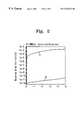
- FIG. 2is a graph illustrating electrical characteristics of a P-N junction in a prior semiconductor device.
- a ‘C’ curvedepicts reverse bias current at an abnormal junction
- a ‘D’ curvedepicts reverse bias current at a normal junction. It is shown that the reverse bias current at the abnormal junction is greater than the reverse bias current at the normal junction.
- a method consistent with the present inventionprovides for a semiconductor device capable of forming a stable P-N junction by isolating lattice defects, such as a dislocation, an extended defect, and a stacking fault, from a P-N junction area.
- lattice defectssuch as a dislocation, an extended defect, and a stacking fault
- a gate electrodeis formed on a semiconductor substrate.
- a conductive impurityis implanted into the semiconductor substrate on both sides of the gate electrode to form a source/drain area.
- a non-conductive impurityis implanted into the source/drain area to form a precipitate area.
- a first conductive impurityis implanted into a semiconductor substrate to form a well area.
- a gate electrodeis formed on the well area.
- a first non-conductive impurityis implanted into the well area on both sides of the gate electrode to form a first precipitate area to a first depth.
- a second conductive impurityis implanted into the well area on both sides of the gate electrode to form a source/drain area to a second depth which can be relatively shallower than the first depth.
- a second non-conductive impurityis implanted into the source/drain area to form a second precipitate area.
- a transistor consistent with the present inventioncomprises a first conductive well area formed in a semiconductor substrate, a first precipitate area formed to a first depth by implanting a first non-conductive impurity into the first conductive well, a gate electrode formed on the first conductive well, a second conductive source/drain area formed in the first well area on both sides of the gate electrode to a second depth which can be relatively shallower than the first depth, and a second precipitate area formed by implanting a second non-conductive impurity into the source/drain area.
- a first non-conductive impurityis implanted into the well area to form a first precipitate area which can control substrate defects.
- a second non-conductive impurityis implanted into the source/drain area to form a second precipitate area which can also control substrate defects.
- FIG. 1Ais an XTEM (X-transmission electron microscopy) photograph illustrating a defect in a prior semiconductor substrate
- FIG. 1Bis an SEM (scanning electron microscopy) photograph illustrating a defect in a prior semiconductor substrate
- FIG. 2is a graph illustrating electrical characteristics of a P-N junction in a prior semiconductor device.
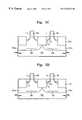
- FIGS. 3A through 3Dare flow diagrams illustrating the process steps of fabricating a MOS transistor consistent with the present invention.
- FIGS. 3A through 3Dsequentially illustrate the process steps of fabricating a MOS transistor according to the present invention.
- a device isolation area 102is formed on a semiconductor substrate 100 to define active and inactive areas.
- the device isolation area 102may be formed of, for example, STI (shallow trench isolation).
- the active areasare divided into PMOS and NMOS areas.
- an N-type impurity ionis implanted into the PMOS area so that an N-type well area 104 a is formed
- a P-type impurity ionis implanted into the NMOS area so that a P-type well area 104 b is formed.
- a first nonconductive impurityis implanted into an overall surface of the semiconductor substrate 100 , so that a first precipitate area 106 is formed on the N-type and the P-type well areas 104 a and 104 b , respectively. Since the first non-conductive impurity can be formed from a material selected from a group consisting of oxygen, carbon, and nitrogen, the first precipitate area can be formed from a material selected from a group consisting of SiO 2 , SiC, and SiN.
- the first non-conductive impurityshould be formed on a stable area having no electrical polarity by implanting impurity such as oxygen and comprising a chemical compound with the semiconductor substrate 100 , and a precipitate area comprising only itself. Further, an implanting concentration of the first non-conductive impurity should be more than the solid solubility (10 18 atoms/cm 3 ) of the semiconductor substrate 100 (i.e., silicon substrate), and less than a concentration at which the first precipitate area 106 may form an undesirable layer. If the concentration of oxygen implanted into the first non-conductive impurity is too high, a new SiO 2 layer making, a SIMOX (separation by implanted oxygen) structure is formed.
- the concentration of oxygen that is implantedshould be so low enough to ensure that the semiconductor substrate 100 is not formed with this structure.
- a method of controlling implanting concentrationis well described in U.S. Pat. No. 4,749,660, which is incorporated herein by reference.
- a gate electrode 108is formed on the semiconductor substrate 100 with a gate oxide layer interposed therebetween.
- a low concentration of a conductive impurity ion for forming an LDD (low doped drain)is implanted into the semiconductor substrate 100 of the active area using the gate electrode 108 as a mask, so that a low concentrated source/drain area 110 is formed.
- a P-type impurity ionis implanted into the N-type well area, and an N-type impurity ion is implanted into the P-type well area.
- a spacer 109is formed on both sidewalls of the gate electrode 108 .
- the silicon nitride layeris anisotropically etched to form a spacer 109 .
- a high concentration of a conductive impurity ion for reducing sheet resistance and contact resistanceis implanted using the spacer 109 and the gate electrode 108 as a mask, so that a high concentrated source/drain area 114 is formed.
- a P-type impurity ionis implanted into an N-type well area, and an N-type impurity ion is implanted into a P-type well area.
- the high and low concentrated source/drain areas 114 and 110are formed in the semiconductor substrate 100 with an equal depth, or the high concentrated source/drain area 114 is formed to be relatively deeper than the low concentrated source/drain area 110 .
- the high concentrated source/drain area 114is preferably formed to be shallower than the first precipitate area 106 .
- a second non-conductive impurityis implanted by using the gate electrode 108 and the spacer 109 as a mask, so that a second precipitate area 116 is formed.
- the second non-conductive impuritycan be formed from a material selected from a group consisting of oxygen, carbon, and nitrogen.
- the implanted concentration of the second non-conductive impurityshould be more than the solid solubility (10 18 atoms/cm 3 ) of the semiconductor substrate 100 (i.e., silicon substrate), and less than a concentration at which the second precipitate area 116 may form an undesirable layer.
- the depth of the second precipitate area 116is preferably shallower than that of the high concentrated source/drain area 114 .
- the first and second precipitate areas 106 and 116which are formed by implanting the non-conductive impurity, may serve the following functions:
- a small overlaying defect and a dislocation loopare generated by a lattice defect due to the ion implantation, a lattice defect due to the STI stress, and an amorphous layer. Afterwards, these grow into substrate defects, such as an extended defect and a dislocation.
- the ion implanting defectis well described, for example, in “Ion Implantation Science and Technology” J. F. Ziegler, pp. 63-92, Academic Press 1988.
- ⁇is a strain of a semiconductor substrate
- ais a radius of a spherical ace in a semiconductor substrate
- a′is the size of a precipitate.
- Formula 1illustrates a strain generated by letting an elastic body of radius a into a spherical space in a emiconductor substrate of radius′.
- Uiis an energy operating between an electric potential of a substrate defect and a precipitate of radius a′
- Gis an elastic coefficient of a semiconductor substrate (i.e., a silicon substrate)
- bis a degree of the dislocation
- ais a radius, which is almost similar to the radius of a precipitate of a spherical space
- ris a distance between the precipitate and the electric potential
- ⁇is the strain in Formula 1.
- Formula 2is described in “Impurities and Imperfections” E. R. Parker, J. Washburn, ASM, Metals Park, Ohio, p. 155, 1955.
- a MOS transistor of this inventioncomprises well areas 104 a and 104 b formed in the semiconductor substrate 100 , a first precipitate area 106 formed in the well areas 104 a and 104 b , a gate electrode 108 formed in the well areas 104 a and 104 b , source/drain areas 110 and 114 formed in well areas 104 a and 104 b on both sides of the gate electrode, wherein the source/drain areas 110 and 114 can be shallower than the first precipitate area 106 in depth, and a second precipitate area 116 is formed in the source/drain area 110 and 114 .
- a force, reacting to the precipitatemay generate a dislocation. Then, the force enables the dislocation, as the substrate defect, to be pulled out of the precipitate or not to be grown further.
- the substrate defectsmay go away from an interface of the P-N junction. As a result, it is impossible for the substrate defects to penetrate the interface thereof, and the interface damage generated by the substrate defects is prevented.
- a P-N junction areamay be damaged by substrate defects such as dislocation in a prior semiconductor device, the P-N junction area results in abnormal reverse bias current characteristics.
- a precipitate area, however, formed adjacent to the P-N junction area in the present inventionprevents growth of the substrate defects and damage to the P-N junction area.
Landscapes
- Physics & Mathematics (AREA)
- Engineering & Computer Science (AREA)
- High Energy & Nuclear Physics (AREA)
- General Physics & Mathematics (AREA)
- Toxicology (AREA)
- Condensed Matter Physics & Semiconductors (AREA)
- Health & Medical Sciences (AREA)
- Manufacturing & Machinery (AREA)
- Computer Hardware Design (AREA)
- Microelectronics & Electronic Packaging (AREA)
- Power Engineering (AREA)
- Insulated Gate Type Field-Effect Transistor (AREA)
- Metal-Oxide And Bipolar Metal-Oxide Semiconductor Integrated Circuits (AREA)
Abstract
Description
1. Field of the Invention
The present invention relates to a method for fabricating a semiconductor device and, more particularly, to a method for fabricating a MOS transistor capable of reducing P-N junction leakage current generated by substrate defects.
2. Background of the Invention
As the integration level of semiconductor memory devices increases, the integration level is progressing to a DRAM (dynamic random access memory) device having a size of a gigabit or more. Since components of a gigabit unit device are scaled down to less than 0.18 μm, the likelihood that stress may occur increases greatly.
If the stress surpasses a critical value, dislocation may be generated in the device's silicon substrate to relieve the stress. Due to the scaling down, the process of forming a device isolation area converts a LOCOS (local oxidation of silicon) into an STI (shallow trench isolation). However, the STI may apply more stress to the semiconductor substrate than the LOCOS. As mentioned in an article entitled “Stress-induced Dislocation in Silicon Integrated Circuits” (P. M. Fahey et al., IBM J. RES. DEVELOP, v. 36, p. 158, 1992), it is increasingly reported to improve junction damage generated by dislocation and extended defect.
In the fabricating process of a semiconductor, the ion implanting technique is important in the method for fabricating a P-N junction of a device due to the easy implementation of a doping concentration and a doping profile. However, ions having high energy can penetrate a single crystalline silicon during this ion implanting process. If the doping concentration surpasses a critical value, then the crystallinity of the silicon substrate is broken to form an amorphous layer. The crystallinity of the amorphous layer is restored through a subsequent annealing step. During the annealing, remaining defects are collected to generate an extended defect, a stacking fault, and a dislocation loop (as discussed, for example, in “Formation of Extended Deffects in Silicon by High Energy Implantation of B and P”, J. Y. Cheng et. al., Phys. v. 80 (4) p. 2105, 1996; “Annealing Behaviours of Dislocation Loops Near the Projected Range in High-dose As-Implanted (001) Si”, S. N. Hsu et. al., J Appi. Phys. v. 86 (9). p. 4503, 1990).
FIG. 1A is an XTEM (X-transmission electron microscopy) photograph illustrating a defect in a prior semiconductor substrate. Referring to FIG. 1A, if the dislocation, extended defect, and stacking fault penetrate a P-N junction area ‘A’ of a semiconductor device, then abnormal junction characteristics are generated.
FIG. 1B is an SEM (scanning electron microscopy) photograph illustrating a defect in a prior semiconductor substrate. Referring to FIG. 1B, defects are generated in an edge portion ‘B’ adjacent to a device isolation area and an active area due to the ion implanting process. If a reverse bias voltage is applied to the P-N junction, the reverse bias current to the P-N junction is abnormally applied due to the defects.
FIG. 2 is a graph illustrating electrical characteristics of a P-N junction in a prior semiconductor device. Referring to FIG. 2, in the case that a reverse bias voltage is applied to the P-N junction of the prior semiconductor device, a ‘C’ curve depicts reverse bias current at an abnormal junction, and a ‘D’ curve depicts reverse bias current at a normal junction. It is shown that the reverse bias current at the abnormal junction is greater than the reverse bias current at the normal junction. These characteristics may increase standby current, which may create a severe problem in fabricating a low power consumption device, result in failing components, and reduce yield.
A method consistent with the present invention provides for a semiconductor device capable of forming a stable P-N junction by isolating lattice defects, such as a dislocation, an extended defect, and a stacking fault, from a P-N junction area.
According to the present invention, a gate electrode is formed on a semiconductor substrate. A conductive impurity is implanted into the semiconductor substrate on both sides of the gate electrode to form a source/drain area. A non-conductive impurity is implanted into the source/drain area to form a precipitate area.
According to another aspect of the present invention, a first conductive impurity is implanted into a semiconductor substrate to form a well area. A gate electrode is formed on the well area. A first non-conductive impurity is implanted into the well area on both sides of the gate electrode to form a first precipitate area to a first depth. A second conductive impurity is implanted into the well area on both sides of the gate electrode to form a source/drain area to a second depth which can be relatively shallower than the first depth. A second non-conductive impurity is implanted into the source/drain area to form a second precipitate area.
A transistor consistent with the present invention comprises a first conductive well area formed in a semiconductor substrate, a first precipitate area formed to a first depth by implanting a first non-conductive impurity into the first conductive well, a gate electrode formed on the first conductive well, a second conductive source/drain area formed in the first well area on both sides of the gate electrode to a second depth which can be relatively shallower than the first depth, and a second precipitate area formed by implanting a second non-conductive impurity into the source/drain area.
In the method consistent with the present invention, a first non-conductive impurity is implanted into the well area to form a first precipitate area which can control substrate defects. A second non-conductive impurity is implanted into the source/drain area to form a second precipitate area which can also control substrate defects. As a result, substrate defects such as dislocation, extended defect, and stacking fault are isolated from a P-N junction area, thereby forming a stable P-N junction.
These and other features, aspects, and advantages of the present invention will become better understood with regard to the following description, appended claims, and accompanying drawings where:
FIG. 1A is an XTEM (X-transmission electron microscopy) photograph illustrating a defect in a prior semiconductor substrate;
FIG. 1B is an SEM (scanning electron microscopy) photograph illustrating a defect in a prior semiconductor substrate;
FIG. 2 is a graph illustrating electrical characteristics of a P-N junction in a prior semiconductor device; and
FIGS. 3A through 3D are flow diagrams illustrating the process steps of fabricating a MOS transistor consistent with the present invention.
The preferred embodiment of the present invention is described in greater detail with reference to accompanying drawings. In addition, Korean application no. 98-26582, filed Jul. 2, 1998, is hereby incorporated by reference as if fully set forth herein.
FIGS. 3A through 3D sequentially illustrate the process steps of fabricating a MOS transistor according to the present invention.
Referring to FIG. 3A, adevice isolation area 102 is formed on asemiconductor substrate 100 to define active and inactive areas. Thedevice isolation area 102 may be formed of, for example, STI (shallow trench isolation). The active areas are divided into PMOS and NMOS areas. Conventionally, an N-type impurity ion is implanted into the PMOS area so that an N-type well area 104ais formed, and a P-type impurity ion is implanted into the NMOS area so that a P-type well area 104bis formed. A first nonconductive impurity is implanted into an overall surface of thesemiconductor substrate 100, so that a first precipitatearea 106 is formed on the N-type and the P-type well areas
The first non-conductive impurity should be formed on a stable area having no electrical polarity by implanting impurity such as oxygen and comprising a chemical compound with thesemiconductor substrate 100, and a precipitate area comprising only itself. Further, an implanting concentration of the first non-conductive impurity should be more than the solid solubility (1018atoms/cm3) of the semiconductor substrate100 (i.e., silicon substrate), and less than a concentration at which the first precipitatearea 106 may form an undesirable layer. If the concentration of oxygen implanted into the first non-conductive impurity is too high, a new SiO2layer making, a SIMOX (separation by implanted oxygen) structure is formed. It is undesirable to form a new layer such as an SiO2layer. Accordingly, the concentration of oxygen that is implanted should be so low enough to ensure that thesemiconductor substrate 100 is not formed with this structure. A method of controlling implanting concentration is well described in U.S. Pat. No. 4,749,660, which is incorporated herein by reference.
Referring to FIG. 3B, agate electrode 108 is formed on thesemiconductor substrate 100 with a gate oxide layer interposed therebetween. A low concentration of a conductive impurity ion for forming an LDD (low doped drain) is implanted into thesemiconductor substrate 100 of the active area using thegate electrode 108 as a mask, so that a low concentrated source/drain area 110 is formed. A P-type impurity ion is implanted into the N-type well area, and an N-type impurity ion is implanted into the P-type well area.
Next, referring to FIG. 3C, aspacer 109 is formed on both sidewalls of thegate electrode 108. For example, after formation of a silicon nitride layer on thesemiconductor substrate 100 including thegate electrode 108, the silicon nitride layer is anisotropically etched to form aspacer 109.
A high concentration of a conductive impurity ion for reducing sheet resistance and contact resistance is implanted using thespacer 109 and thegate electrode 108 as a mask, so that a high concentrated source/drain area 114 is formed. A P-type impurity ion is implanted into an N-type well area, and an N-type impurity ion is implanted into a P-type well area. Then, the high and low concentrated source/drain areas semiconductor substrate 100 with an equal depth, or the high concentrated source/drain area 114 is formed to be relatively deeper than the low concentrated source/drain area 110. The high concentrated source/drain area 114 is preferably formed to be shallower than the first precipitatearea 106.
Next, referring to FIG. 3D, a second non-conductive impurity is implanted by using thegate electrode 108 and thespacer 109 as a mask, so that a second precipitatearea 116 is formed. The second non-conductive impurity can be formed from a material selected from a group consisting of oxygen, carbon, and nitrogen. Like the first non-conductive impurity, the implanted concentration of the second non-conductive impurity should be more than the solid solubility (1018atoms/cm3) of the semiconductor substrate100 (i.e., silicon substrate), and less than a concentration at which the second precipitatearea 116 may form an undesirable layer. The depth of the second precipitatearea 116 is preferably shallower than that of the high concentrated source/drain area 114.
The first and second precipitateareas
A small overlaying defect and a dislocation loop are generated by a lattice defect due to the ion implantation, a lattice defect due to the STI stress, and an amorphous layer. Afterwards, these grow into substrate defects, such as an extended defect and a dislocation. The ion implanting defect is well described, for example, in “Ion Implantation Science and Technology” J. F. Ziegler, pp. 63-92, Academic Press 1988.
InFormula 1, ∈ is a strain of a semiconductor substrate, a is a radius of a spherical ace in a semiconductor substrate, and a′ is the size of a precipitate.Formula 1 illustrates a strain generated by letting an elastic body of radius a into a spherical space in a emiconductor substrate of radius′.
InFormula 2, Ui is an energy operating between an electric potential of a substrate defect and a precipitate of radius a′, G is an elastic coefficient of a semiconductor substrate (i.e., a silicon substrate), b is a degree of the dislocation, a is a radius, which is almost similar to the radius of a precipitate of a spherical space, r is a distance between the precipitate and the electric potential, and ∈ is the strain inFormula 1.Formula 2 is described in “Impurities and Imperfections” E. R. Parker, J. Washburn, ASM, Metals Park, Ohio, p. 155, 1955.
Referring to FIG. 3D, a MOS transistor of this invention comprises wellareas semiconductor substrate 100, a first precipitatearea 106 formed in thewell areas gate electrode 108 formed in thewell areas drain areas well areas drain areas area 106 in depth, and a second precipitatearea 116 is formed in the source/drain area
If a precipitate area, as inFormula 2, is in a single crystalline form of silicon, a force, reacting to the precipitate, may generate a dislocation. Then, the force enables the dislocation, as the substrate defect, to be pulled out of the precipitate or not to be grown further. In case the precipitate is formed at a bit of distance from the P-N junction, the substrate defects may go away from an interface of the P-N junction. As a result, it is impossible for the substrate defects to penetrate the interface thereof, and the interface damage generated by the substrate defects is prevented.
Since a P-N junction area may be damaged by substrate defects such as dislocation in a prior semiconductor device, the P-N junction area results in abnormal reverse bias current characteristics. A precipitate area, however, formed adjacent to the P-N junction area in the present invention prevents growth of the substrate defects and damage to the P-N junction area.
Claims (10)
1. A method for fabricating a MOS transistor, comprising:
forming a gate electrode on a semiconductor substrate;
implanting a conductive impurity into the semiconductor substrate on both sides of the gate electrode to form a source/drain area; and
implanting a non-conductive impurity into the source/drain area to form a precipitate area, wherein the implanting concentration of the non-conductive impurity is in the range between 1×10¹⁸atom/cm3and 1×10²⁰atoms/cm3, a value sufficient to suppress formation of a SiO2layer in SIMOX (separation by implanted oxygen).
2. The method according toclaim 1 , wherein the non-conductive impurity is a material selected from the group consisting of oxygen, carbon, and nitrogen.
3. The method according toclaim 1 , wherein the precipitate area prevents the formation of semiconductor substrate defects.
4. A method for fabricating a MOS transistor, comprising:
implanting a first conductive impurity ion into a semiconductor substrate to form a well area;
implanting a first non-conductive impurity into the well area to form a first precipitate area to a first depth in the well area;
forming a gate electrode on the well area;
implanting a second conductive impurity into the well area on both sides of the gate electrode to form a source/drain area to a second depth, the second depth being relatively shallower than the first depth; and
implanting a second non-conductive impurity into the source/drain area to form a second precipitate area to a third depth, the third depth being relatively shallower than the second depth.
5. The method according toclaim 4 , wherein the non-conductive impurity is a material selected from the group consisting of oxygen, carbon, and nitrogen.
6. The method according toclaim 4 , wherein the second non-conductive impurity is a material selected from the group consisting of oxygen, carbon, and nitrogen.
7. The method according toclaim 4 , wherein an implanting concentration of the first non-conductive impurity is in the range between 1×10⁸atom/cm3and 1×10²⁰atoms/cm3, a value sufficient to suppress formation of a SiO2layer in SIMOX (separation by implanted oxygen).
8. The method according toclaim 4 , wherein an implanting concentration of the second non-conductive impurity is in the range between 1×10¹⁸atom/cm3and 1×10²⁰atoms/cm3, a value sufficient to suppress formation of a SiO2layer in SIMOX (separation by implanted oxygen).
9. The method according toclaim 4 , wherein the first precipitate area prevents the formation of semiconductor substrate defects.
10. The method according toclaim 4 , wherein the second precipitate area prevents the formation of semiconductor substrate defects.
Applications Claiming Priority (2)
| Application Number | Priority Date | Filing Date | Title |
|---|---|---|---|
| KR98-26582 | 1998-07-02 | ||
| KR1019980026582AKR100292818B1 (en) | 1998-07-02 | 1998-07-02 | MOS transistor manufacturing method |
Publications (1)
| Publication Number | Publication Date |
|---|---|
| US6335233B1true US6335233B1 (en) | 2002-01-01 |
Family
ID=19542815
Family Applications (1)
| Application Number | Title | Priority Date | Filing Date |
|---|---|---|---|
| US09/347,822Expired - Fee RelatedUS6335233B1 (en) | 1998-07-02 | 1999-07-02 | Method for fabricating MOS transistor |
Country Status (5)
| Country | Link |
|---|---|
| US (1) | US6335233B1 (en) |
| JP (1) | JP2000036597A (en) |
| KR (1) | KR100292818B1 (en) |
| CN (1) | CN1146968C (en) |
| TW (1) | TW418534B (en) |
Cited By (57)
| Publication number | Priority date | Publication date | Assignee | Title |
|---|---|---|---|---|
| US20040056314A1 (en)* | 2002-09-19 | 2004-03-25 | Tatsuya Ohguro | Semiconductor device in which occurrence of slips is suppressed |
| US20040155317A1 (en)* | 2003-02-10 | 2004-08-12 | Arup Bhattacharyya | Transistor constructions and electronic devices |
| US20040253776A1 (en)* | 2003-06-12 | 2004-12-16 | Thomas Hoffmann | Gate-induced strain for MOS performance improvement |
| US20050014351A1 (en)* | 2003-03-31 | 2005-01-20 | Weber Cory E. | Nitrogen controlled growth of dislocation loop in stress enhanced transistor |
| US20050076941A1 (en)* | 2003-10-10 | 2005-04-14 | Brad Larson | Ergonomic collapsible crutch |
| US20060003510A1 (en)* | 2004-06-30 | 2006-01-05 | Thorsten Kammler | Technique for transferring strain into a semiconductor region |
| US20060006427A1 (en)* | 2004-07-07 | 2006-01-12 | Tan Chung F | Material architecture for the fabrication of low temperature transistor |
| US20060046415A1 (en)* | 2004-08-25 | 2006-03-02 | Kabushiki Kaisha Toshiba | Semiconductor device and manufacturing method for the same |
| US20080128764A1 (en)* | 2006-11-30 | 2008-06-05 | Samsung Electronics Co., Ltd. | Semiconductor substrate including a plurality of insulating regions, semiconductor device having the same, and method of manufacturing the device |
| US20080188043A1 (en)* | 2006-12-26 | 2008-08-07 | Renesas Technology Corp. | Method of manufacturing a semiconductor device |
| EP2293338A2 (en) | 2003-06-16 | 2011-03-09 | Intel Corporation | Double-gate transistor with enhanced carrier mobility field |
| US20110121404A1 (en)* | 2009-09-30 | 2011-05-26 | Lucian Shifren | Advanced transistors with punch through suppression |
| US8404551B2 (en) | 2010-12-03 | 2013-03-26 | Suvolta, Inc. | Source/drain extension control for advanced transistors |
| US8461875B1 (en) | 2011-02-18 | 2013-06-11 | Suvolta, Inc. | Digital circuits having improved transistors, and methods therefor |
| US8525271B2 (en) | 2011-03-03 | 2013-09-03 | Suvolta, Inc. | Semiconductor structure with improved channel stack and method for fabrication thereof |
| US8530286B2 (en) | 2010-04-12 | 2013-09-10 | Suvolta, Inc. | Low power semiconductor transistor structure and method of fabrication thereof |
| US8569128B2 (en) | 2010-06-21 | 2013-10-29 | Suvolta, Inc. | Semiconductor structure and method of fabrication thereof with mixed metal types |
| US8569156B1 (en) | 2011-05-16 | 2013-10-29 | Suvolta, Inc. | Reducing or eliminating pre-amorphization in transistor manufacture |
| US8599623B1 (en) | 2011-12-23 | 2013-12-03 | Suvolta, Inc. | Circuits and methods for measuring circuit elements in an integrated circuit device |
| US8614128B1 (en) | 2011-08-23 | 2013-12-24 | Suvolta, Inc. | CMOS structures and processes based on selective thinning |
| US8629016B1 (en) | 2011-07-26 | 2014-01-14 | Suvolta, Inc. | Multiple transistor types formed in a common epitaxial layer by differential out-diffusion from a doped underlayer |
| US8637955B1 (en) | 2012-08-31 | 2014-01-28 | Suvolta, Inc. | Semiconductor structure with reduced junction leakage and method of fabrication thereof |
| US8645878B1 (en) | 2011-08-23 | 2014-02-04 | Suvolta, Inc. | Porting a circuit design from a first semiconductor process to a second semiconductor process |
| US8713511B1 (en) | 2011-09-16 | 2014-04-29 | Suvolta, Inc. | Tools and methods for yield-aware semiconductor manufacturing process target generation |
| US8735987B1 (en) | 2011-06-06 | 2014-05-27 | Suvolta, Inc. | CMOS gate stack structures and processes |
| US8748270B1 (en) | 2011-03-30 | 2014-06-10 | Suvolta, Inc. | Process for manufacturing an improved analog transistor |
| US8748986B1 (en) | 2011-08-05 | 2014-06-10 | Suvolta, Inc. | Electronic device with controlled threshold voltage |
| US8759872B2 (en) | 2010-06-22 | 2014-06-24 | Suvolta, Inc. | Transistor with threshold voltage set notch and method of fabrication thereof |
| US8796048B1 (en) | 2011-05-11 | 2014-08-05 | Suvolta, Inc. | Monitoring and measurement of thin film layers |
| US8811068B1 (en) | 2011-05-13 | 2014-08-19 | Suvolta, Inc. | Integrated circuit devices and methods |
| US8816754B1 (en) | 2012-11-02 | 2014-08-26 | Suvolta, Inc. | Body bias circuits and methods |
| US8819603B1 (en) | 2011-12-15 | 2014-08-26 | Suvolta, Inc. | Memory circuits and methods of making and designing the same |
| US8863064B1 (en) | 2012-03-23 | 2014-10-14 | Suvolta, Inc. | SRAM cell layout structure and devices therefrom |
| US8877619B1 (en) | 2012-01-23 | 2014-11-04 | Suvolta, Inc. | Process for manufacture of integrated circuits with different channel doping transistor architectures and devices therefrom |
| US8883600B1 (en) | 2011-12-22 | 2014-11-11 | Suvolta, Inc. | Transistor having reduced junction leakage and methods of forming thereof |
| US8895327B1 (en) | 2011-12-09 | 2014-11-25 | Suvolta, Inc. | Tipless transistors, short-tip transistors, and methods and circuits therefor |
| US8970289B1 (en) | 2012-01-23 | 2015-03-03 | Suvolta, Inc. | Circuits and devices for generating bi-directional body bias voltages, and methods therefor |
| US8995204B2 (en) | 2011-06-23 | 2015-03-31 | Suvolta, Inc. | Circuit devices and methods having adjustable transistor body bias |
| US8999861B1 (en) | 2011-05-11 | 2015-04-07 | Suvolta, Inc. | Semiconductor structure with substitutional boron and method for fabrication thereof |
| US9041126B2 (en) | 2012-09-21 | 2015-05-26 | Mie Fujitsu Semiconductor Limited | Deeply depleted MOS transistors having a screening layer and methods thereof |
| US9054219B1 (en) | 2011-08-05 | 2015-06-09 | Mie Fujitsu Semiconductor Limited | Semiconductor devices having fin structures and fabrication methods thereof |
| US9070477B1 (en) | 2012-12-12 | 2015-06-30 | Mie Fujitsu Semiconductor Limited | Bit interleaved low voltage static random access memory (SRAM) and related methods |
| US9093550B1 (en) | 2012-01-31 | 2015-07-28 | Mie Fujitsu Semiconductor Limited | Integrated circuits having a plurality of high-K metal gate FETs with various combinations of channel foundation structure and gate stack structure and methods of making same |
| US9093997B1 (en) | 2012-11-15 | 2015-07-28 | Mie Fujitsu Semiconductor Limited | Slew based process and bias monitors and related methods |
| US9112484B1 (en) | 2012-12-20 | 2015-08-18 | Mie Fujitsu Semiconductor Limited | Integrated circuit process and bias monitors and related methods |
| US9112057B1 (en) | 2012-09-18 | 2015-08-18 | Mie Fujitsu Semiconductor Limited | Semiconductor devices with dopant migration suppression and method of fabrication thereof |
| US9236466B1 (en) | 2011-10-07 | 2016-01-12 | Mie Fujitsu Semiconductor Limited | Analog circuits having improved insulated gate transistors, and methods therefor |
| US9268885B1 (en) | 2013-02-28 | 2016-02-23 | Mie Fujitsu Semiconductor Limited | Integrated circuit device methods and models with predicted device metric variations |
| US9299801B1 (en) | 2013-03-14 | 2016-03-29 | Mie Fujitsu Semiconductor Limited | Method for fabricating a transistor device with a tuned dopant profile |
| US9299698B2 (en) | 2012-06-27 | 2016-03-29 | Mie Fujitsu Semiconductor Limited | Semiconductor structure with multiple transistors having various threshold voltages |
| US9319013B2 (en) | 2014-08-19 | 2016-04-19 | Mie Fujitsu Semiconductor Limited | Operational amplifier input offset correction with transistor threshold voltage adjustment |
| US9406567B1 (en) | 2012-02-28 | 2016-08-02 | Mie Fujitsu Semiconductor Limited | Method for fabricating multiple transistor devices on a substrate with varying threshold voltages |
| US9412859B2 (en) | 2013-03-11 | 2016-08-09 | Globalfoundries Inc. | Contact geometry having a gate silicon length decoupled from a transistor length |
| US9431068B2 (en) | 2012-10-31 | 2016-08-30 | Mie Fujitsu Semiconductor Limited | Dynamic random access memory (DRAM) with low variation transistor peripheral circuits |
| US9478571B1 (en) | 2013-05-24 | 2016-10-25 | Mie Fujitsu Semiconductor Limited | Buried channel deeply depleted channel transistor |
| US9710006B2 (en) | 2014-07-25 | 2017-07-18 | Mie Fujitsu Semiconductor Limited | Power up body bias circuits and methods |
| US10074568B2 (en) | 2009-09-30 | 2018-09-11 | Mie Fujitsu Semiconductor Limited | Electronic devices and systems, and methods for making and using same |
Families Citing this family (1)
| Publication number | Priority date | Publication date | Assignee | Title |
|---|---|---|---|---|
| JP4015068B2 (en) | 2003-06-17 | 2007-11-28 | 株式会社東芝 | Manufacturing method of semiconductor device |
Citations (13)
| Publication number | Priority date | Publication date | Assignee | Title |
|---|---|---|---|---|
| US4700454A (en)* | 1985-11-04 | 1987-10-20 | Intel Corporation | Process for forming MOS transistor with buried oxide regions for insulation |
| US4749660A (en)* | 1986-11-26 | 1988-06-07 | American Telephone And Telegraph Company, At&T Bell Laboratories | Method of making an article comprising a buried SiO2 layer |
| US5288650A (en)* | 1991-01-25 | 1994-02-22 | Ibis Technology Corporation | Prenucleation process for simox device fabrication |
| US5468657A (en)* | 1994-06-17 | 1995-11-21 | Sharp Microelectronics Technology, Inc. | Nitridation of SIMOX buried oxide |
| US5554546A (en)* | 1993-01-04 | 1996-09-10 | Texas Instruments Inc. | Method of fabricating a high voltage transistor |
| US5658809A (en)* | 1994-03-23 | 1997-08-19 | Komatsu Electronic Metals Co., Ltd. | SOI substrate and method of producing the same |
| US5795800A (en)* | 1995-06-07 | 1998-08-18 | Sgs-Thomson Microelectronics, Inc. | Integrated circuit fabrication method with buried oxide isolation |
| US5872049A (en)* | 1996-06-19 | 1999-02-16 | Advanced Micro Devices, Inc. | Nitrogenated gate structure for improved transistor performance and method for making same |
| US5877048A (en)* | 1998-03-23 | 1999-03-02 | Texas Instruments--Acer Incorporated | 3-D CMOS transistors with high ESD reliability |
| US5930642A (en)* | 1997-06-09 | 1999-07-27 | Advanced Micro Devices, Inc. | Transistor with buried insulative layer beneath the channel region |
| US5970347A (en)* | 1997-07-18 | 1999-10-19 | Advanced Micro Devices, Inc. | High performance mosfet transistor fabrication technique |
| US6011290A (en)* | 1998-01-20 | 2000-01-04 | Advanced Micro Devices | Short channel length MOSFET transistor |
| US6030875A (en)* | 1997-12-19 | 2000-02-29 | Advanced Micro Devices, Inc. | Method for making semiconductor device having nitrogen-rich active region-channel interface |
Family Cites Families (1)
| Publication number | Priority date | Publication date | Assignee | Title |
|---|---|---|---|---|
| JPS59205759A (en)* | 1983-04-01 | 1984-11-21 | Hitachi Ltd | MIS type field effect transistor |
- 1998
- 1998-07-02KRKR1019980026582Apatent/KR100292818B1/ennot_activeExpired - Fee Related
- 1999
- 1999-04-16TWTW088106098Apatent/TW418534B/ennot_activeIP Right Cessation
- 1999-06-29CNCNB991094123Apatent/CN1146968C/ennot_activeExpired - Fee Related
- 1999-07-02JPJP11189591Apatent/JP2000036597A/enactivePending
- 1999-07-02USUS09/347,822patent/US6335233B1/ennot_activeExpired - Fee Related
Patent Citations (14)
| Publication number | Priority date | Publication date | Assignee | Title |
|---|---|---|---|---|
| US4700454A (en)* | 1985-11-04 | 1987-10-20 | Intel Corporation | Process for forming MOS transistor with buried oxide regions for insulation |
| US4749660A (en)* | 1986-11-26 | 1988-06-07 | American Telephone And Telegraph Company, At&T Bell Laboratories | Method of making an article comprising a buried SiO2 layer |
| US5288650A (en)* | 1991-01-25 | 1994-02-22 | Ibis Technology Corporation | Prenucleation process for simox device fabrication |
| US5554546A (en)* | 1993-01-04 | 1996-09-10 | Texas Instruments Inc. | Method of fabricating a high voltage transistor |
| US5658809A (en)* | 1994-03-23 | 1997-08-19 | Komatsu Electronic Metals Co., Ltd. | SOI substrate and method of producing the same |
| US5468657A (en)* | 1994-06-17 | 1995-11-21 | Sharp Microelectronics Technology, Inc. | Nitridation of SIMOX buried oxide |
| US5795800A (en)* | 1995-06-07 | 1998-08-18 | Sgs-Thomson Microelectronics, Inc. | Integrated circuit fabrication method with buried oxide isolation |
| US5795800B1 (en)* | 1995-06-07 | 2000-03-28 | Sgs Thomson Microelectronics | Integrated circuit fabrication method with buried oxide isolation |
| US5872049A (en)* | 1996-06-19 | 1999-02-16 | Advanced Micro Devices, Inc. | Nitrogenated gate structure for improved transistor performance and method for making same |
| US5930642A (en)* | 1997-06-09 | 1999-07-27 | Advanced Micro Devices, Inc. | Transistor with buried insulative layer beneath the channel region |
| US5970347A (en)* | 1997-07-18 | 1999-10-19 | Advanced Micro Devices, Inc. | High performance mosfet transistor fabrication technique |
| US6030875A (en)* | 1997-12-19 | 2000-02-29 | Advanced Micro Devices, Inc. | Method for making semiconductor device having nitrogen-rich active region-channel interface |
| US6011290A (en)* | 1998-01-20 | 2000-01-04 | Advanced Micro Devices | Short channel length MOSFET transistor |
| US5877048A (en)* | 1998-03-23 | 1999-03-02 | Texas Instruments--Acer Incorporated | 3-D CMOS transistors with high ESD reliability |
Cited By (130)
| Publication number | Priority date | Publication date | Assignee | Title |
|---|---|---|---|---|
| US6885069B2 (en)* | 2002-09-19 | 2005-04-26 | Kabushiki Kaisha Toshiba | Semiconductor device in which occurrence of slips is suppressed |
| US20040056314A1 (en)* | 2002-09-19 | 2004-03-25 | Tatsuya Ohguro | Semiconductor device in which occurrence of slips is suppressed |
| US20050167757A1 (en)* | 2002-09-19 | 2005-08-04 | Kabushiki Kaisha Toshiba | Semiconductor device in which occurence of slips is suppressed |
| US20050247982A1 (en)* | 2003-02-10 | 2005-11-10 | Arup Bhattacharyya | Transistor constructions and electronic devices |
| US20040155317A1 (en)* | 2003-02-10 | 2004-08-12 | Arup Bhattacharyya | Transistor constructions and electronic devices |
| US7291519B2 (en) | 2003-02-10 | 2007-11-06 | Micron Technology, Inc. | Methods of forming transistor constructions |
| US7115948B2 (en) | 2003-02-10 | 2006-10-03 | Micron Technology, Inc. | Transistor constructions and electronic devices |
| US20060125010A1 (en)* | 2003-02-10 | 2006-06-15 | Arup Bhattacharyya | Methods of forming transistor constructions |
| US7042052B2 (en)* | 2003-02-10 | 2006-05-09 | Micron Technology, Inc. | Transistor constructions and electronic devices |
| US7187057B2 (en)* | 2003-03-31 | 2007-03-06 | Intel Corporation | Nitrogen controlled growth of dislocation loop in stress enhanced transistor |
| US7226824B2 (en)* | 2003-03-31 | 2007-06-05 | Intel Corporation | Nitrogen controlled growth of dislocation loop in stress enhanced transistor |
| US20050014351A1 (en)* | 2003-03-31 | 2005-01-20 | Weber Cory E. | Nitrogen controlled growth of dislocation loop in stress enhanced transistor |
| US20050017309A1 (en)* | 2003-03-31 | 2005-01-27 | Weber Cory E. | Nitrogen controlled growth of dislocation loop in stress enhanced transistor |
| US20050167652A1 (en)* | 2003-06-12 | 2005-08-04 | Thomas Hoffmann | Gate-induced strain for MOS performance improvement |
| US7452764B2 (en) | 2003-06-12 | 2008-11-18 | Intel Corporation | Gate-induced strain for MOS performance improvement |
| US6982433B2 (en) | 2003-06-12 | 2006-01-03 | Intel Corporation | Gate-induced strain for MOS performance improvement |
| US20040253776A1 (en)* | 2003-06-12 | 2004-12-16 | Thomas Hoffmann | Gate-induced strain for MOS performance improvement |
| EP2273547A2 (en) | 2003-06-12 | 2011-01-12 | Intel Corporation | Gate-induced strain for performance improvement of a cmos semiconductor apparatus |
| EP2293338A2 (en) | 2003-06-16 | 2011-03-09 | Intel Corporation | Double-gate transistor with enhanced carrier mobility field |
| US20050076941A1 (en)* | 2003-10-10 | 2005-04-14 | Brad Larson | Ergonomic collapsible crutch |
| US20060003510A1 (en)* | 2004-06-30 | 2006-01-05 | Thorsten Kammler | Technique for transferring strain into a semiconductor region |
| US7494906B2 (en)* | 2004-06-30 | 2009-02-24 | Advanced Micro Devices, Inc. | Technique for transferring strain into a semiconductor region |
| US20060006427A1 (en)* | 2004-07-07 | 2006-01-12 | Tan Chung F | Material architecture for the fabrication of low temperature transistor |
| US7169675B2 (en)* | 2004-07-07 | 2007-01-30 | Chartered Semiconductor Manufacturing, Ltd | Material architecture for the fabrication of low temperature transistor |
| US7514763B2 (en)* | 2004-08-25 | 2009-04-07 | Kabushiki Kaisha Toshiba | Semiconductor device and manufacturing method for the same |
| US7271443B2 (en)* | 2004-08-25 | 2007-09-18 | Kabushiki Kaisha Toshiba | Semiconductor device and manufacturing method for the same |
| US20080176373A1 (en)* | 2004-08-25 | 2008-07-24 | Kabushiki Kaisha Toshiba | Semiconductor device and manufacturing method for the same |
| US20080067633A1 (en)* | 2004-08-25 | 2008-03-20 | Kabushiki Kaisha Toshiba | Semiconductor device and manufacturing method for the same |
| US20060046415A1 (en)* | 2004-08-25 | 2006-03-02 | Kabushiki Kaisha Toshiba | Semiconductor device and manufacturing method for the same |
| US20090159939A1 (en)* | 2004-08-25 | 2009-06-25 | Kabushiki Kaisha Toshiba | Semiconductor device and manufacturing method for the same |
| US7605043B2 (en)* | 2004-08-25 | 2009-10-20 | Kabushiki Kaisha Toshiba | Semiconductor device and manufacturing method for the same |
| US20080128764A1 (en)* | 2006-11-30 | 2008-06-05 | Samsung Electronics Co., Ltd. | Semiconductor substrate including a plurality of insulating regions, semiconductor device having the same, and method of manufacturing the device |
| US7674668B2 (en)* | 2006-12-26 | 2010-03-09 | Renesas Technology Corp. | Method of manufacturing a semiconductor device |
| US20080188043A1 (en)* | 2006-12-26 | 2008-08-07 | Renesas Technology Corp. | Method of manufacturing a semiconductor device |
| US10074568B2 (en) | 2009-09-30 | 2018-09-11 | Mie Fujitsu Semiconductor Limited | Electronic devices and systems, and methods for making and using same |
| US9508800B2 (en) | 2009-09-30 | 2016-11-29 | Mie Fujitsu Semiconductor Limited | Advanced transistors with punch through suppression |
| US8421162B2 (en) | 2009-09-30 | 2013-04-16 | Suvolta, Inc. | Advanced transistors with punch through suppression |
| US20110121404A1 (en)* | 2009-09-30 | 2011-05-26 | Lucian Shifren | Advanced transistors with punch through suppression |
| US9263523B2 (en) | 2009-09-30 | 2016-02-16 | Mie Fujitsu Semiconductor Limited | Advanced transistors with punch through suppression |
| US11062950B2 (en) | 2009-09-30 | 2021-07-13 | United Semiconductor Japan Co., Ltd. | Electronic devices and systems, and methods for making and using the same |
| US10217668B2 (en) | 2009-09-30 | 2019-02-26 | Mie Fujitsu Semiconductor Limited | Electronic devices and systems, and methods for making and using the same |
| US10224244B2 (en) | 2009-09-30 | 2019-03-05 | Mie Fujitsu Semiconductor Limited | Electronic devices and systems, and methods for making and using the same |
| US10325986B2 (en) | 2009-09-30 | 2019-06-18 | Mie Fujitsu Semiconductor Limited | Advanced transistors with punch through suppression |
| US11887895B2 (en) | 2009-09-30 | 2024-01-30 | United Semiconductor Japan Co., Ltd. | Electronic devices and systems, and methods for making and using the same |
| US8530286B2 (en) | 2010-04-12 | 2013-09-10 | Suvolta, Inc. | Low power semiconductor transistor structure and method of fabrication thereof |
| US9496261B2 (en) | 2010-04-12 | 2016-11-15 | Mie Fujitsu Semiconductor Limited | Low power semiconductor transistor structure and method of fabrication thereof |
| US9865596B2 (en) | 2010-04-12 | 2018-01-09 | Mie Fujitsu Semiconductor Limited | Low power semiconductor transistor structure and method of fabrication thereof |
| US8569128B2 (en) | 2010-06-21 | 2013-10-29 | Suvolta, Inc. | Semiconductor structure and method of fabrication thereof with mixed metal types |
| US9224733B2 (en) | 2010-06-21 | 2015-12-29 | Mie Fujitsu Semiconductor Limited | Semiconductor structure and method of fabrication thereof with mixed metal types |
| US9418987B2 (en) | 2010-06-22 | 2016-08-16 | Mie Fujitsu Semiconductor Limited | Transistor with threshold voltage set notch and method of fabrication thereof |
| US9922977B2 (en) | 2010-06-22 | 2018-03-20 | Mie Fujitsu Semiconductor Limited | Transistor with threshold voltage set notch and method of fabrication thereof |
| US8759872B2 (en) | 2010-06-22 | 2014-06-24 | Suvolta, Inc. | Transistor with threshold voltage set notch and method of fabrication thereof |
| US8563384B2 (en) | 2010-12-03 | 2013-10-22 | Suvolta, Inc. | Source/drain extension control for advanced transistors |
| US8686511B2 (en) | 2010-12-03 | 2014-04-01 | Suvolta, Inc. | Source/drain extension control for advanced transistors |
| US9006843B2 (en) | 2010-12-03 | 2015-04-14 | Suvolta, Inc. | Source/drain extension control for advanced transistors |
| US8404551B2 (en) | 2010-12-03 | 2013-03-26 | Suvolta, Inc. | Source/drain extension control for advanced transistors |
| US8461875B1 (en) | 2011-02-18 | 2013-06-11 | Suvolta, Inc. | Digital circuits having improved transistors, and methods therefor |
| US9184750B1 (en) | 2011-02-18 | 2015-11-10 | Mie Fujitsu Semiconductor Limited | Digital circuits having improved transistors, and methods therefor |
| US9838012B2 (en) | 2011-02-18 | 2017-12-05 | Mie Fujitsu Semiconductor Limited | Digital circuits having improved transistors, and methods therefor |
| US9680470B2 (en) | 2011-02-18 | 2017-06-13 | Mie Fujitsu Semiconductor Limited | Digital circuits having improved transistors, and methods therefor |
| US9985631B2 (en) | 2011-02-18 | 2018-05-29 | Mie Fujitsu Semiconductor Limited | Digital circuits having improved transistors, and methods therefor |
| US10250257B2 (en) | 2011-02-18 | 2019-04-02 | Mie Fujitsu Semiconductor Limited | Digital circuits having improved transistors, and methods therefor |
| US9111785B2 (en) | 2011-03-03 | 2015-08-18 | Mie Fujitsu Semiconductor Limited | Semiconductor structure with improved channel stack and method for fabrication thereof |
| US8525271B2 (en) | 2011-03-03 | 2013-09-03 | Suvolta, Inc. | Semiconductor structure with improved channel stack and method for fabrication thereof |
| US9093469B2 (en) | 2011-03-30 | 2015-07-28 | Mie Fujitsu Semiconductor Limited | Analog transistor |
| US8748270B1 (en) | 2011-03-30 | 2014-06-10 | Suvolta, Inc. | Process for manufacturing an improved analog transistor |
| US8999861B1 (en) | 2011-05-11 | 2015-04-07 | Suvolta, Inc. | Semiconductor structure with substitutional boron and method for fabrication thereof |
| US8796048B1 (en) | 2011-05-11 | 2014-08-05 | Suvolta, Inc. | Monitoring and measurement of thin film layers |
| US9741428B2 (en) | 2011-05-13 | 2017-08-22 | Mie Fujitsu Semiconductor Limited | Integrated circuit devices and methods |
| US9362291B1 (en) | 2011-05-13 | 2016-06-07 | Mie Fujitsu Semiconductor Limited | Integrated circuit devices and methods |
| US8811068B1 (en) | 2011-05-13 | 2014-08-19 | Suvolta, Inc. | Integrated circuit devices and methods |
| US9966130B2 (en) | 2011-05-13 | 2018-05-08 | Mie Fujitsu Semiconductor Limited | Integrated circuit devices and methods |
| US9514940B2 (en) | 2011-05-16 | 2016-12-06 | Mie Fujitsu Semiconductor Limited | Reducing or eliminating pre-amorphization in transistor manufacture |
| US8569156B1 (en) | 2011-05-16 | 2013-10-29 | Suvolta, Inc. | Reducing or eliminating pre-amorphization in transistor manufacture |
| US8937005B2 (en) | 2011-05-16 | 2015-01-20 | Suvolta, Inc. | Reducing or eliminating pre-amorphization in transistor manufacture |
| US9793172B2 (en) | 2011-05-16 | 2017-10-17 | Mie Fujitsu Semiconductor Limited | Reducing or eliminating pre-amorphization in transistor manufacture |
| US8735987B1 (en) | 2011-06-06 | 2014-05-27 | Suvolta, Inc. | CMOS gate stack structures and processes |
| US9281248B1 (en) | 2011-06-06 | 2016-03-08 | Mie Fujitsu Semiconductor Limited | CMOS gate stack structures and processes |
| US8995204B2 (en) | 2011-06-23 | 2015-03-31 | Suvolta, Inc. | Circuit devices and methods having adjustable transistor body bias |
| US8916937B1 (en) | 2011-07-26 | 2014-12-23 | Suvolta, Inc. | Multiple transistor types formed in a common epitaxial layer by differential out-diffusion from a doped underlayer |
| US8629016B1 (en) | 2011-07-26 | 2014-01-14 | Suvolta, Inc. | Multiple transistor types formed in a common epitaxial layer by differential out-diffusion from a doped underlayer |
| US8653604B1 (en) | 2011-07-26 | 2014-02-18 | Suvolta, Inc. | Multiple transistor types formed in a common epitaxial layer by differential out-diffusion from a doped underlayer |
| US9054219B1 (en) | 2011-08-05 | 2015-06-09 | Mie Fujitsu Semiconductor Limited | Semiconductor devices having fin structures and fabrication methods thereof |
| US8963249B1 (en) | 2011-08-05 | 2015-02-24 | Suvolta, Inc. | Electronic device with controlled threshold voltage |
| US8748986B1 (en) | 2011-08-05 | 2014-06-10 | Suvolta, Inc. | Electronic device with controlled threshold voltage |
| US9117746B1 (en) | 2011-08-23 | 2015-08-25 | Mie Fujitsu Semiconductor Limited | Porting a circuit design from a first semiconductor process to a second semiconductor process |
| US8806395B1 (en) | 2011-08-23 | 2014-08-12 | Suvolta, Inc. | Porting a circuit design from a first semiconductor process to a second semiconductor process |
| US9391076B1 (en) | 2011-08-23 | 2016-07-12 | Mie Fujitsu Semiconductor Limited | CMOS structures and processes based on selective thinning |
| US8645878B1 (en) | 2011-08-23 | 2014-02-04 | Suvolta, Inc. | Porting a circuit design from a first semiconductor process to a second semiconductor process |
| US8614128B1 (en) | 2011-08-23 | 2013-12-24 | Suvolta, Inc. | CMOS structures and processes based on selective thinning |
| US8713511B1 (en) | 2011-09-16 | 2014-04-29 | Suvolta, Inc. | Tools and methods for yield-aware semiconductor manufacturing process target generation |
| US9236466B1 (en) | 2011-10-07 | 2016-01-12 | Mie Fujitsu Semiconductor Limited | Analog circuits having improved insulated gate transistors, and methods therefor |
| US8895327B1 (en) | 2011-12-09 | 2014-11-25 | Suvolta, Inc. | Tipless transistors, short-tip transistors, and methods and circuits therefor |
| US8819603B1 (en) | 2011-12-15 | 2014-08-26 | Suvolta, Inc. | Memory circuits and methods of making and designing the same |
| US8883600B1 (en) | 2011-12-22 | 2014-11-11 | Suvolta, Inc. | Transistor having reduced junction leakage and methods of forming thereof |
| US9196727B2 (en) | 2011-12-22 | 2015-11-24 | Mie Fujitsu Semiconductor Limited | High uniformity screen and epitaxial layers for CMOS devices |
| US9368624B2 (en) | 2011-12-22 | 2016-06-14 | Mie Fujitsu Semiconductor Limited | Method for fabricating a transistor with reduced junction leakage current |
| US8599623B1 (en) | 2011-12-23 | 2013-12-03 | Suvolta, Inc. | Circuits and methods for measuring circuit elements in an integrated circuit device |
| US8877619B1 (en) | 2012-01-23 | 2014-11-04 | Suvolta, Inc. | Process for manufacture of integrated circuits with different channel doping transistor architectures and devices therefrom |
| US8970289B1 (en) | 2012-01-23 | 2015-03-03 | Suvolta, Inc. | Circuits and devices for generating bi-directional body bias voltages, and methods therefor |
| US9093550B1 (en) | 2012-01-31 | 2015-07-28 | Mie Fujitsu Semiconductor Limited | Integrated circuits having a plurality of high-K metal gate FETs with various combinations of channel foundation structure and gate stack structure and methods of making same |
| US9385047B2 (en) | 2012-01-31 | 2016-07-05 | Mie Fujitsu Semiconductor Limited | Integrated circuits having a plurality of high-K metal gate FETs with various combinations of channel foundation structure and gate stack structure and methods of making same |
| US9406567B1 (en) | 2012-02-28 | 2016-08-02 | Mie Fujitsu Semiconductor Limited | Method for fabricating multiple transistor devices on a substrate with varying threshold voltages |
| US8863064B1 (en) | 2012-03-23 | 2014-10-14 | Suvolta, Inc. | SRAM cell layout structure and devices therefrom |
| US10014387B2 (en) | 2012-06-27 | 2018-07-03 | Mie Fujitsu Semiconductor Limited | Semiconductor structure with multiple transistors having various threshold voltages |
| US9299698B2 (en) | 2012-06-27 | 2016-03-29 | Mie Fujitsu Semiconductor Limited | Semiconductor structure with multiple transistors having various threshold voltages |
| US9812550B2 (en) | 2012-06-27 | 2017-11-07 | Mie Fujitsu Semiconductor Limited | Semiconductor structure with multiple transistors having various threshold voltages |
| US10217838B2 (en) | 2012-06-27 | 2019-02-26 | Mie Fujitsu Semiconductor Limited | Semiconductor structure with multiple transistors having various threshold voltages |
| US8637955B1 (en) | 2012-08-31 | 2014-01-28 | Suvolta, Inc. | Semiconductor structure with reduced junction leakage and method of fabrication thereof |
| US9105711B2 (en) | 2012-08-31 | 2015-08-11 | Mie Fujitsu Semiconductor Limited | Semiconductor structure with reduced junction leakage and method of fabrication thereof |
| US9112057B1 (en) | 2012-09-18 | 2015-08-18 | Mie Fujitsu Semiconductor Limited | Semiconductor devices with dopant migration suppression and method of fabrication thereof |
| US9041126B2 (en) | 2012-09-21 | 2015-05-26 | Mie Fujitsu Semiconductor Limited | Deeply depleted MOS transistors having a screening layer and methods thereof |
| US9431068B2 (en) | 2012-10-31 | 2016-08-30 | Mie Fujitsu Semiconductor Limited | Dynamic random access memory (DRAM) with low variation transistor peripheral circuits |
| US8816754B1 (en) | 2012-11-02 | 2014-08-26 | Suvolta, Inc. | Body bias circuits and methods |
| US9154123B1 (en) | 2012-11-02 | 2015-10-06 | Mie Fujitsu Semiconductor Limited | Body bias circuits and methods |
| US9093997B1 (en) | 2012-11-15 | 2015-07-28 | Mie Fujitsu Semiconductor Limited | Slew based process and bias monitors and related methods |
| US9319034B2 (en) | 2012-11-15 | 2016-04-19 | Mie Fujitsu Semiconductor Limited | Slew based process and bias monitors and related methods |
| US9070477B1 (en) | 2012-12-12 | 2015-06-30 | Mie Fujitsu Semiconductor Limited | Bit interleaved low voltage static random access memory (SRAM) and related methods |
| US9276561B2 (en) | 2012-12-20 | 2016-03-01 | Mie Fujitsu Semiconductor Limited | Integrated circuit process and bias monitors and related methods |
| US9112484B1 (en) | 2012-12-20 | 2015-08-18 | Mie Fujitsu Semiconductor Limited | Integrated circuit process and bias monitors and related methods |
| US9268885B1 (en) | 2013-02-28 | 2016-02-23 | Mie Fujitsu Semiconductor Limited | Integrated circuit device methods and models with predicted device metric variations |
| US9412859B2 (en) | 2013-03-11 | 2016-08-09 | Globalfoundries Inc. | Contact geometry having a gate silicon length decoupled from a transistor length |
| US9893148B2 (en) | 2013-03-14 | 2018-02-13 | Mie Fujitsu Semiconductor Limited | Method for fabricating a transistor device with a tuned dopant profile |
| US9577041B2 (en) | 2013-03-14 | 2017-02-21 | Mie Fujitsu Semiconductor Limited | Method for fabricating a transistor device with a tuned dopant profile |
| US9299801B1 (en) | 2013-03-14 | 2016-03-29 | Mie Fujitsu Semiconductor Limited | Method for fabricating a transistor device with a tuned dopant profile |
| US9478571B1 (en) | 2013-05-24 | 2016-10-25 | Mie Fujitsu Semiconductor Limited | Buried channel deeply depleted channel transistor |
| US9991300B2 (en) | 2013-05-24 | 2018-06-05 | Mie Fujitsu Semiconductor Limited | Buried channel deeply depleted channel transistor |
| US9786703B2 (en) | 2013-05-24 | 2017-10-10 | Mie Fujitsu Semiconductor Limited | Buried channel deeply depleted channel transistor |
| US9710006B2 (en) | 2014-07-25 | 2017-07-18 | Mie Fujitsu Semiconductor Limited | Power up body bias circuits and methods |
| US9319013B2 (en) | 2014-08-19 | 2016-04-19 | Mie Fujitsu Semiconductor Limited | Operational amplifier input offset correction with transistor threshold voltage adjustment |
Also Published As
| Publication number | Publication date |
|---|---|
| TW418534B (en) | 2001-01-11 |
| KR100292818B1 (en) | 2001-11-05 |
| CN1146968C (en) | 2004-04-21 |
| JP2000036597A (en) | 2000-02-02 |
| KR20000007303A (en) | 2000-02-07 |
| CN1241020A (en) | 2000-01-12 |
Similar Documents
| Publication | Publication Date | Title |
|---|---|---|
| US6335233B1 (en) | Method for fabricating MOS transistor | |
| US8129246B2 (en) | Advanced CMOS using super steep retrograde wells | |
| US6531739B2 (en) | Radiation-hardened silicon-on-insulator CMOS device, and method of making the same | |
| US6335251B2 (en) | Semiconductor apparatus having elevated source and drain structure and manufacturing method therefor | |
| US5910676A (en) | Method for forming a thick base oxide in a BiCMOS process | |
| US9514940B2 (en) | Reducing or eliminating pre-amorphization in transistor manufacture | |
| US7943471B1 (en) | Diode with asymmetric silicon germanium anode | |
| JPH1197674A (en) | Semiconductor device and manufacturing method thereof | |
| US20030219954A1 (en) | Manufacturing method of semiconductor substrate | |
| EP1815520B1 (en) | Method of forming a silicon-on-insulator semiconductor device with silicon layer having defferent crystal orientations | |
| US5923070A (en) | Semiconductor device having an element inclusion region for reducing stress caused by lattice mismatch | |
| US20110180881A1 (en) | Integration scheme for reducing border region morphology in hybrid orientation technology (hot) using direct silicon bonded (dsb) substrates | |
| US4863878A (en) | Method of making silicon on insalator material using oxygen implantation | |
| US7524710B2 (en) | Radiation-hardened silicon-on-insulator CMOS device, and method of making the same | |
| CN113206108B (en) | Semiconductor-on-insulator substrate, semiconductor structure and method for forming the same | |
| US6699771B1 (en) | Process for optimizing junctions formed by solid phase epitaxy | |
| TW418507B (en) | A semiconductor device | |
| US6362054B1 (en) | Method for fabricating MOS device with halo implanted region | |
| US6720632B2 (en) | Semiconductor device having diffusion layer formed using dopant of large mass number | |
| JP2004006821A (en) | Bipolar transistor | |
| US6828614B2 (en) | Semiconductor constructions, and methods of forming semiconductor constructions | |
| JPH0737893A (en) | Semiconductor device and manufacturing method thereof | |
| EP0409041B1 (en) | A method for forming a thick base oxide in a BiCMOS process | |
| EP0791957A2 (en) | Semiconductor substrate and method of manufacturing the same | |
| JPH06296019A (en) | Semiconductor device and manufacturing method thereof |
Legal Events
| Date | Code | Title | Description |
|---|---|---|---|
| AS | Assignment | Owner name:SAMSUNG ELECTRONICS CO., LTD., KOREA, REPUBLIC OF Free format text:ASSIGNMENT OF ASSIGNORS INTEREST;ASSIGNORS:CHO, CHANG-HYUN;KOH, GWAN-HYEOB;LEE, MI-HYANG;AND OTHERS;REEL/FRAME:010096/0750 Effective date:19990626 | |
| FEPP | Fee payment procedure | Free format text:PAYOR NUMBER ASSIGNED (ORIGINAL EVENT CODE: ASPN); ENTITY STATUS OF PATENT OWNER: LARGE ENTITY | |
| FPAY | Fee payment | Year of fee payment:4 | |
| FEPP | Fee payment procedure | Free format text:PAYER NUMBER DE-ASSIGNED (ORIGINAL EVENT CODE: RMPN); ENTITY STATUS OF PATENT OWNER: LARGE ENTITY Free format text:PAYOR NUMBER ASSIGNED (ORIGINAL EVENT CODE: ASPN); ENTITY STATUS OF PATENT OWNER: LARGE ENTITY | |
| FPAY | Fee payment | Year of fee payment:8 | |
| REMI | Maintenance fee reminder mailed | ||
| LAPS | Lapse for failure to pay maintenance fees | ||
| STCH | Information on status: patent discontinuation | Free format text:PATENT EXPIRED DUE TO NONPAYMENT OF MAINTENANCE FEES UNDER 37 CFR 1.362 | |
| FP | Lapsed due to failure to pay maintenance fee | Effective date:20140101 |