US6335224B1 - Protection of microelectronic devices during packaging - Google Patents
Protection of microelectronic devices during packagingDownload PDFInfo
- Publication number
- US6335224B1 US6335224B1US09/572,562US57256200AUS6335224B1US 6335224 B1US6335224 B1US 6335224B1US 57256200 AUS57256200 AUS 57256200AUS 6335224 B1US6335224 B1US 6335224B1
- Authority
- US
- United States
- Prior art keywords
- protective coating
- wafer
- coating
- sensitive area
- packaging
- Prior art date
- Legal status (The legal status is an assumption and is not a legal conclusion. Google has not performed a legal analysis and makes no representation as to the accuracy of the status listed.)
- Expired - Lifetime
Links
- 238000004806packaging method and processMethods0.000titleclaimsabstractdescription29
- 238000004377microelectronicMethods0.000titleclaimsabstractdescription28
- 238000000034methodMethods0.000claimsabstractdescription90
- 239000011253protective coatingSubstances0.000claimsabstractdescription76
- 229920000052poly(p-xylylene)Polymers0.000claimsabstractdescription43
- 239000000463materialSubstances0.000claimsabstractdescription19
- VYPSYNLAJGMNEJ-UHFFFAOYSA-NSilicium dioxideChemical compoundO=[Si]=OVYPSYNLAJGMNEJ-UHFFFAOYSA-N0.000claimsabstractdescription17
- 229920000642polymerPolymers0.000claimsabstractdescription12
- FFUAGWLWBBFQJT-UHFFFAOYSA-NhexamethyldisilazaneChemical compoundC[Si](C)(C)N[Si](C)(C)CFFUAGWLWBBFQJT-UHFFFAOYSA-N0.000claimsabstractdescription9
- 235000012239silicon dioxideNutrition0.000claimsabstractdescription9
- 239000000377silicon dioxideSubstances0.000claimsabstractdescription8
- OKTJSMMVPCPJKN-UHFFFAOYSA-NCarbonChemical compound[C]OKTJSMMVPCPJKN-UHFFFAOYSA-N0.000claimsabstractdescription6
- 229910052799carbonInorganic materials0.000claimsabstractdescription6
- 150000001732carboxylic acid derivativesChemical class0.000claimsabstractdescription6
- 229910052751metalInorganic materials0.000claimsabstractdescription5
- 239000002184metalSubstances0.000claimsabstractdescription5
- 239000010702perfluoropolyetherSubstances0.000claimsabstractdescription5
- 239000005368silicate glassSubstances0.000claimsabstractdescription5
- WFKWXMTUELFFGS-UHFFFAOYSA-NtungstenChemical compound[W]WFKWXMTUELFFGS-UHFFFAOYSA-N0.000claimsabstractdescription4
- 229910052721tungstenInorganic materials0.000claimsabstractdescription4
- 239000010937tungstenSubstances0.000claimsabstractdescription4
- 229910052581Si3N4Inorganic materials0.000claimsabstractdescription3
- 229910052782aluminiumInorganic materials0.000claimsabstractdescription3
- XAGFODPZIPBFFR-UHFFFAOYSA-NaluminiumChemical compound[Al]XAGFODPZIPBFFR-UHFFFAOYSA-N0.000claimsabstractdescription3
- 239000011368organic materialSubstances0.000claimsabstractdescription3
- HQVNEWCFYHHQES-UHFFFAOYSA-Nsilicon nitrideChemical compoundN12[Si]34N5[Si]62N3[Si]51N64HQVNEWCFYHHQES-UHFFFAOYSA-N0.000claimsabstractdescription3
- 238000000576coating methodMethods0.000claimsdescription73
- 239000011248coating agentSubstances0.000claimsdescription50
- 238000000151depositionMethods0.000claimsdescription18
- 238000005520cutting processMethods0.000claimsdescription16
- 238000001312dry etchingMethods0.000claimsdescription14
- 230000008021depositionEffects0.000claimsdescription11
- QVGXLLKOCUKJST-UHFFFAOYSA-Natomic oxygenChemical compound[O]QVGXLLKOCUKJST-UHFFFAOYSA-N0.000claimsdescription7
- 229910052801chlorineInorganic materials0.000claimsdescription7
- 239000007789gasSubstances0.000claimsdescription7
- 239000000314lubricantSubstances0.000claimsdescription7
- 239000000178monomerSubstances0.000claimsdescription7
- 229910052760oxygenInorganic materials0.000claimsdescription7
- 239000001301oxygenSubstances0.000claimsdescription7
- 229910052731fluorineInorganic materials0.000claimsdescription5
- 239000011737fluorineSubstances0.000claimsdescription5
- XUIMIQQOPSSXEZ-UHFFFAOYSA-NSiliconChemical compound[Si]XUIMIQQOPSSXEZ-UHFFFAOYSA-N0.000claimsdescription4
- 125000001309chloro groupChemical groupCl*0.000claimsdescription4
- 150000002500ionsChemical class0.000claimsdescription4
- 229910052710siliconInorganic materials0.000claimsdescription4
- 239000010703siliconSubstances0.000claimsdescription4
- 238000006467substitution reactionMethods0.000claimsdescription4
- ZAMOUSCENKQFHK-UHFFFAOYSA-NChlorine atomChemical compound[Cl]ZAMOUSCENKQFHK-UHFFFAOYSA-N0.000claimsdescription3
- CBENFWSGALASAD-UHFFFAOYSA-NOzoneChemical compound[O-][O+]=OCBENFWSGALASAD-UHFFFAOYSA-N0.000claimsdescription3
- 239000000460chlorineSubstances0.000claimsdescription3
- 238000000623plasma-assisted chemical vapour depositionMethods0.000claimsdescription3
- KZBUYRJDOAKODT-UHFFFAOYSA-NChlorineChemical compoundClClKZBUYRJDOAKODT-UHFFFAOYSA-N0.000claimsdescription2
- 229920001577copolymerPolymers0.000claimsdescription2
- 230000002401inhibitory effectEffects0.000claimsdescription2
- 230000005855radiationEffects0.000claimsdescription2
- 238000000992sputter etchingMethods0.000claimsdescription2
- PXGOKWXKJXAPGV-UHFFFAOYSA-NFluorineChemical compoundFFPXGOKWXKJXAPGV-UHFFFAOYSA-N0.000claims2
- 238000005229chemical vapour depositionMethods0.000claims2
- 238000002156mixingMethods0.000claims1
- 230000000379polymerizing effectEffects0.000claims1
- 238000001020plasma etchingMethods0.000abstractdescription6
- 235000012431wafersNutrition0.000description33
- 230000006378damageEffects0.000description11
- 238000005530etchingMethods0.000description9
- 239000000758substrateSubstances0.000description8
- VRBFTYUMFJWSJY-UHFFFAOYSA-N28804-46-8Chemical compoundClC1CC(C=C2)=CC=C2C(Cl)CC2=CC=C1C=C2VRBFTYUMFJWSJY-UHFFFAOYSA-N0.000description7
- 239000011521glassSubstances0.000description7
- 239000007788liquidSubstances0.000description7
- 238000001039wet etchingMethods0.000description7
- 239000010410layerSubstances0.000description6
- 229910021420polycrystalline siliconInorganic materials0.000description6
- 239000000126substanceSubstances0.000description6
- 239000002253acidSubstances0.000description5
- 238000004519manufacturing processMethods0.000description5
- 239000000203mixtureSubstances0.000description5
- 239000004033plasticSubstances0.000description5
- 229920003023plasticPolymers0.000description5
- 229920005591polysiliconPolymers0.000description5
- VEXZGXHMUGYJMC-UHFFFAOYSA-NHydrochloric acidChemical compoundClVEXZGXHMUGYJMC-UHFFFAOYSA-N0.000description4
- 230000000694effectsEffects0.000description4
- 230000003287optical effectEffects0.000description4
- 238000012545processingMethods0.000description4
- 238000012360testing methodMethods0.000description4
- 239000004593EpoxySubstances0.000description3
- KRHYYFGTRYWZRS-UHFFFAOYSA-NFluoraneChemical compoundFKRHYYFGTRYWZRS-UHFFFAOYSA-N0.000description3
- 238000013459approachMethods0.000description3
- 238000004140cleaningMethods0.000description3
- 238000011109contaminationMethods0.000description3
- 238000001035dryingMethods0.000description3
- -1fluorine ionsChemical class0.000description3
- 239000002904solventSubstances0.000description3
- 150000007513acidsChemical class0.000description2
- 230000015572biosynthetic processEffects0.000description2
- 238000009530blood pressure measurementMethods0.000description2
- 238000009529body temperature measurementMethods0.000description2
- 239000003054catalystSubstances0.000description2
- 238000005137deposition processMethods0.000description2
- 229910003460diamondInorganic materials0.000description2
- 239000010432diamondSubstances0.000description2
- 239000000428dustSubstances0.000description2
- 239000003112inhibitorSubstances0.000description2
- 238000007689inspectionMethods0.000description2
- 238000000608laser ablationMethods0.000description2
- 238000003754machiningMethods0.000description2
- 230000000873masking effectEffects0.000description2
- 238000001465metallisationMethods0.000description2
- 229920000647polyepoxidePolymers0.000description2
- 239000000843powderSubstances0.000description2
- 238000002360preparation methodMethods0.000description2
- 238000007789sealingMethods0.000description2
- 239000002094self assembled monolayerSubstances0.000description2
- 239000004065semiconductorSubstances0.000description2
- 229910000679solderInorganic materials0.000description2
- 238000001179sorption measurementMethods0.000description2
- JTPNRXUCIXHOKM-UHFFFAOYSA-N1-chloronaphthaleneChemical compoundC1=CC=C2C(Cl)=CC=CC2=C1JTPNRXUCIXHOKM-UHFFFAOYSA-N0.000description1
- OOLUVSIJOMLOCB-UHFFFAOYSA-N1633-22-3Chemical compoundC1CC(C=C2)=CC=C2CCC2=CC=C1C=C2OOLUVSIJOMLOCB-UHFFFAOYSA-N0.000description1
- ZOXJGFHDIHLPTG-UHFFFAOYSA-NBoronChemical compound[B]ZOXJGFHDIHLPTG-UHFFFAOYSA-N0.000description1
- YCKRFDGAMUMZLT-UHFFFAOYSA-NFluorine atomChemical compound[F]YCKRFDGAMUMZLT-UHFFFAOYSA-N0.000description1
- GYHNNYVSQQEPJS-UHFFFAOYSA-NGalliumChemical compound[Ga]GYHNNYVSQQEPJS-UHFFFAOYSA-N0.000description1
- GRYLNZFGIOXLOG-UHFFFAOYSA-NNitric acidChemical compoundO[N+]([O-])=OGRYLNZFGIOXLOG-UHFFFAOYSA-N0.000description1
- 241000321453Paranthias colonusSpecies0.000description1
- 239000004809TeflonSubstances0.000description1
- 229920006362Teflon®Polymers0.000description1
- 238000002679ablationMethods0.000description1
- 229920006397acrylic thermoplasticPolymers0.000description1
- 229910003481amorphous carbonInorganic materials0.000description1
- 238000004458analytical methodMethods0.000description1
- 238000000429assemblyMethods0.000description1
- 230000000712assemblyEffects0.000description1
- 230000004888barrier functionEffects0.000description1
- 238000009835boilingMethods0.000description1
- 229910052796boronInorganic materials0.000description1
- 238000012512characterization methodMethods0.000description1
- 150000001875compoundsChemical class0.000description1
- 238000007796conventional methodMethods0.000description1
- 239000002178crystalline materialSubstances0.000description1
- 239000002173cutting fluidSubstances0.000description1
- 239000000539dimerSubstances0.000description1
- 239000006185dispersionSubstances0.000description1
- 230000009977dual effectEffects0.000description1
- 238000004100electronic packagingMethods0.000description1
- 125000003700epoxy groupChemical group0.000description1
- 229920006336epoxy molding compoundPolymers0.000description1
- 239000003822epoxy resinSubstances0.000description1
- 230000007717exclusionEffects0.000description1
- 230000001747exhibiting effectEffects0.000description1
- 238000013100final testMethods0.000description1
- 230000009969flowable effectEffects0.000description1
- 239000012530fluidSubstances0.000description1
- 238000009472formulationMethods0.000description1
- 229910052733galliumInorganic materials0.000description1
- 238000012685gas phase polymerizationMethods0.000description1
- PCHJSUWPFVWCPO-UHFFFAOYSA-NgoldChemical compound[Au]PCHJSUWPFVWCPO-UHFFFAOYSA-N0.000description1
- 239000010931goldSubstances0.000description1
- 229910052737goldInorganic materials0.000description1
- BHEPBYXIRTUNPN-UHFFFAOYSA-Nhydridophosphorus(.) (triplet)Chemical compound[PH]BHEPBYXIRTUNPN-UHFFFAOYSA-N0.000description1
- 238000007654immersionMethods0.000description1
- 230000000415inactivating effectEffects0.000description1
- 238000009434installationMethods0.000description1
- 238000009413insulationMethods0.000description1
- 238000002032lab-on-a-chipMethods0.000description1
- 239000011344liquid materialSubstances0.000description1
- 239000007791liquid phaseSubstances0.000description1
- 239000006193liquid solutionSubstances0.000description1
- 239000012528membraneSubstances0.000description1
- 230000005499meniscusEffects0.000description1
- 238000005459micromachiningMethods0.000description1
- QPJSUIGXIBEQAC-UHFFFAOYSA-Nn-(2,4-dichloro-5-propan-2-yloxyphenyl)acetamideChemical compoundCC(C)OC1=CC(NC(C)=O)=C(Cl)C=C1ClQPJSUIGXIBEQAC-UHFFFAOYSA-N0.000description1
- 238000010943off-gassingMethods0.000description1
- 239000003960organic solventSubstances0.000description1
- 238000000059patterningMethods0.000description1
- 230000035699permeabilityEffects0.000description1
- 238000000206photolithographyMethods0.000description1
- 229920002120photoresistant polymerPolymers0.000description1
- 230000000704physical effectEffects0.000description1
- 238000007747platingMethods0.000description1
- 229920003229poly(methyl methacrylate)Polymers0.000description1
- 238000006116polymerization reactionMethods0.000description1
- 229920001296polysiloxanePolymers0.000description1
- 239000010453quartzSubstances0.000description1
- 239000002994raw materialSubstances0.000description1
- 230000002829reductive effectEffects0.000description1
- 238000011160researchMethods0.000description1
- 239000000523sampleSubstances0.000description1
- 230000035939shockEffects0.000description1
- 230000002269spontaneous effectEffects0.000description1
- 230000006641stabilisationEffects0.000description1
- 238000011105stabilizationMethods0.000description1
- 230000003068static effectEffects0.000description1
- 238000003860storageMethods0.000description1
- 238000005092sublimation methodMethods0.000description1
- HIFJUMGIHIZEPX-UHFFFAOYSA-Nsulfuric acid;sulfur trioxideChemical compoundO=S(=O)=O.OS(O)(=O)=OHIFJUMGIHIZEPX-UHFFFAOYSA-N0.000description1
- 238000000352supercritical dryingMethods0.000description1
- ISXSCDLOGDJUNJ-UHFFFAOYSA-Ntert-butyl prop-2-enoateChemical compoundCC(C)(C)OC(=O)C=CISXSCDLOGDJUNJ-UHFFFAOYSA-N0.000description1
- BFKJFAAPBSQJPD-UHFFFAOYSA-NtetrafluoroetheneChemical compoundFC(F)=C(F)FBFKJFAAPBSQJPD-UHFFFAOYSA-N0.000description1
- 150000003673urethanesChemical class0.000description1
- 238000001771vacuum depositionMethods0.000description1
- 239000012808vapor phaseSubstances0.000description1
- 238000001947vapour-phase growthMethods0.000description1
- XLYOFNOQVPJJNP-UHFFFAOYSA-NwaterSubstancesOXLYOFNOQVPJJNP-UHFFFAOYSA-N0.000description1
- 229910052724xenonInorganic materials0.000description1
- FHNFHKCVQCLJFQ-UHFFFAOYSA-Nxenon atomChemical compound[Xe]FHNFHKCVQCLJFQ-UHFFFAOYSA-N0.000description1
Images


Classifications
- B—PERFORMING OPERATIONS; TRANSPORTING
- B81—MICROSTRUCTURAL TECHNOLOGY
- B81C—PROCESSES OR APPARATUS SPECIALLY ADAPTED FOR THE MANUFACTURE OR TREATMENT OF MICROSTRUCTURAL DEVICES OR SYSTEMS
- B81C1/00—Manufacture or treatment of devices or systems in or on a substrate
- B81C1/00015—Manufacture or treatment of devices or systems in or on a substrate for manufacturing microsystems
- B81C1/00261—Processes for packaging MEMS devices
- B81C1/00333—Aspects relating to packaging of MEMS devices, not covered by groups B81C1/00269 - B81C1/00325
- B—PERFORMING OPERATIONS; TRANSPORTING
- B81—MICROSTRUCTURAL TECHNOLOGY
- B81C—PROCESSES OR APPARATUS SPECIALLY ADAPTED FOR THE MANUFACTURE OR TREATMENT OF MICROSTRUCTURAL DEVICES OR SYSTEMS
- B81C1/00—Manufacture or treatment of devices or systems in or on a substrate
- B81C1/00865—Multistep processes for the separation of wafers into individual elements
- B81C1/00896—Temporary protection during separation into individual elements
- H—ELECTRICITY
- H01—ELECTRIC ELEMENTS
- H01L—SEMICONDUCTOR DEVICES NOT COVERED BY CLASS H10
- H01L21/00—Processes or apparatus adapted for the manufacture or treatment of semiconductor or solid state devices or of parts thereof
- H01L21/02—Manufacture or treatment of semiconductor devices or of parts thereof
- H01L21/04—Manufacture or treatment of semiconductor devices or of parts thereof the devices having potential barriers, e.g. a PN junction, depletion layer or carrier concentration layer
- H01L21/50—Assembly of semiconductor devices using processes or apparatus not provided for in a single one of the groups H01L21/18 - H01L21/326 or H10D48/04 - H10D48/07 e.g. sealing of a cap to a base of a container
- H01L21/56—Encapsulations, e.g. encapsulation layers, coatings
- H01L21/561—Batch processing
- H—ELECTRICITY
- H01—ELECTRIC ELEMENTS
- H01L—SEMICONDUCTOR DEVICES NOT COVERED BY CLASS H10
- H01L23/00—Details of semiconductor or other solid state devices
- H01L23/28—Encapsulations, e.g. encapsulating layers, coatings, e.g. for protection
- H01L23/29—Encapsulations, e.g. encapsulating layers, coatings, e.g. for protection characterised by the material, e.g. carbon
- H01L23/293—Organic, e.g. plastic
- H—ELECTRICITY
- H01—ELECTRIC ELEMENTS
- H01L—SEMICONDUCTOR DEVICES NOT COVERED BY CLASS H10
- H01L2224/00—Indexing scheme for arrangements for connecting or disconnecting semiconductor or solid-state bodies and methods related thereto as covered by H01L24/00
- H01L2224/01—Means for bonding being attached to, or being formed on, the surface to be connected, e.g. chip-to-package, die-attach, "first-level" interconnects; Manufacturing methods related thereto
- H01L2224/26—Layer connectors, e.g. plate connectors, solder or adhesive layers; Manufacturing methods related thereto
- H01L2224/31—Structure, shape, material or disposition of the layer connectors after the connecting process
- H01L2224/32—Structure, shape, material or disposition of the layer connectors after the connecting process of an individual layer connector
- H01L2224/321—Disposition
- H01L2224/32151—Disposition the layer connector connecting between a semiconductor or solid-state body and an item not being a semiconductor or solid-state body, e.g. chip-to-substrate, chip-to-passive
- H01L2224/32221—Disposition the layer connector connecting between a semiconductor or solid-state body and an item not being a semiconductor or solid-state body, e.g. chip-to-substrate, chip-to-passive the body and the item being stacked
- H01L2224/32225—Disposition the layer connector connecting between a semiconductor or solid-state body and an item not being a semiconductor or solid-state body, e.g. chip-to-substrate, chip-to-passive the body and the item being stacked the item being non-metallic, e.g. insulating substrate with or without metallisation
- H—ELECTRICITY
- H01—ELECTRIC ELEMENTS
- H01L—SEMICONDUCTOR DEVICES NOT COVERED BY CLASS H10
- H01L2224/00—Indexing scheme for arrangements for connecting or disconnecting semiconductor or solid-state bodies and methods related thereto as covered by H01L24/00
- H01L2224/01—Means for bonding being attached to, or being formed on, the surface to be connected, e.g. chip-to-package, die-attach, "first-level" interconnects; Manufacturing methods related thereto
- H01L2224/42—Wire connectors; Manufacturing methods related thereto
- H01L2224/47—Structure, shape, material or disposition of the wire connectors after the connecting process
- H01L2224/48—Structure, shape, material or disposition of the wire connectors after the connecting process of an individual wire connector
- H01L2224/4805—Shape
- H01L2224/4809—Loop shape
- H01L2224/48091—Arched
- H—ELECTRICITY
- H01—ELECTRIC ELEMENTS
- H01L—SEMICONDUCTOR DEVICES NOT COVERED BY CLASS H10
- H01L2224/00—Indexing scheme for arrangements for connecting or disconnecting semiconductor or solid-state bodies and methods related thereto as covered by H01L24/00
- H01L2224/01—Means for bonding being attached to, or being formed on, the surface to be connected, e.g. chip-to-package, die-attach, "first-level" interconnects; Manufacturing methods related thereto
- H01L2224/42—Wire connectors; Manufacturing methods related thereto
- H01L2224/47—Structure, shape, material or disposition of the wire connectors after the connecting process
- H01L2224/48—Structure, shape, material or disposition of the wire connectors after the connecting process of an individual wire connector
- H01L2224/481—Disposition
- H01L2224/48151—Connecting between a semiconductor or solid-state body and an item not being a semiconductor or solid-state body, e.g. chip-to-substrate, chip-to-passive
- H01L2224/48221—Connecting between a semiconductor or solid-state body and an item not being a semiconductor or solid-state body, e.g. chip-to-substrate, chip-to-passive the body and the item being stacked
- H01L2224/48225—Connecting between a semiconductor or solid-state body and an item not being a semiconductor or solid-state body, e.g. chip-to-substrate, chip-to-passive the body and the item being stacked the item being non-metallic, e.g. insulating substrate with or without metallisation
- H01L2224/48227—Connecting between a semiconductor or solid-state body and an item not being a semiconductor or solid-state body, e.g. chip-to-substrate, chip-to-passive the body and the item being stacked the item being non-metallic, e.g. insulating substrate with or without metallisation connecting the wire to a bond pad of the item
- H—ELECTRICITY
- H01—ELECTRIC ELEMENTS
- H01L—SEMICONDUCTOR DEVICES NOT COVERED BY CLASS H10
- H01L2224/00—Indexing scheme for arrangements for connecting or disconnecting semiconductor or solid-state bodies and methods related thereto as covered by H01L24/00
- H01L2224/01—Means for bonding being attached to, or being formed on, the surface to be connected, e.g. chip-to-package, die-attach, "first-level" interconnects; Manufacturing methods related thereto
- H01L2224/42—Wire connectors; Manufacturing methods related thereto
- H01L2224/47—Structure, shape, material or disposition of the wire connectors after the connecting process
- H01L2224/48—Structure, shape, material or disposition of the wire connectors after the connecting process of an individual wire connector
- H01L2224/484—Connecting portions
- H01L2224/48463—Connecting portions the connecting portion on the bonding area of the semiconductor or solid-state body being a ball bond
- H01L2224/48465—Connecting portions the connecting portion on the bonding area of the semiconductor or solid-state body being a ball bond the other connecting portion not on the bonding area being a wedge bond, i.e. ball-to-wedge, regular stitch
- H—ELECTRICITY
- H01—ELECTRIC ELEMENTS
- H01L—SEMICONDUCTOR DEVICES NOT COVERED BY CLASS H10
- H01L2224/00—Indexing scheme for arrangements for connecting or disconnecting semiconductor or solid-state bodies and methods related thereto as covered by H01L24/00
- H01L2224/73—Means for bonding being of different types provided for in two or more of groups H01L2224/10, H01L2224/18, H01L2224/26, H01L2224/34, H01L2224/42, H01L2224/50, H01L2224/63, H01L2224/71
- H01L2224/732—Location after the connecting process
- H01L2224/73251—Location after the connecting process on different surfaces
- H01L2224/73265—Layer and wire connectors
- H—ELECTRICITY
- H01—ELECTRIC ELEMENTS
- H01L—SEMICONDUCTOR DEVICES NOT COVERED BY CLASS H10
- H01L2224/00—Indexing scheme for arrangements for connecting or disconnecting semiconductor or solid-state bodies and methods related thereto as covered by H01L24/00
- H01L2224/80—Methods for connecting semiconductor or other solid state bodies using means for bonding being attached to, or being formed on, the surface to be connected
- H01L2224/83—Methods for connecting semiconductor or other solid state bodies using means for bonding being attached to, or being formed on, the surface to be connected using a layer connector
- H01L2224/83001—Methods for connecting semiconductor or other solid state bodies using means for bonding being attached to, or being formed on, the surface to be connected using a layer connector involving a temporary auxiliary member not forming part of the bonding apparatus
- H—ELECTRICITY
- H01—ELECTRIC ELEMENTS
- H01L—SEMICONDUCTOR DEVICES NOT COVERED BY CLASS H10
- H01L2224/00—Indexing scheme for arrangements for connecting or disconnecting semiconductor or solid-state bodies and methods related thereto as covered by H01L24/00
- H01L2224/80—Methods for connecting semiconductor or other solid state bodies using means for bonding being attached to, or being formed on, the surface to be connected
- H01L2224/85—Methods for connecting semiconductor or other solid state bodies using means for bonding being attached to, or being formed on, the surface to be connected using a wire connector
- H01L2224/85001—Methods for connecting semiconductor or other solid state bodies using means for bonding being attached to, or being formed on, the surface to be connected using a wire connector involving a temporary auxiliary member not forming part of the bonding apparatus, e.g. removable or sacrificial coating, film or substrate
- H—ELECTRICITY
- H01—ELECTRIC ELEMENTS
- H01L—SEMICONDUCTOR DEVICES NOT COVERED BY CLASS H10
- H01L24/00—Arrangements for connecting or disconnecting semiconductor or solid-state bodies; Methods or apparatus related thereto
- H01L24/01—Means for bonding being attached to, or being formed on, the surface to be connected, e.g. chip-to-package, die-attach, "first-level" interconnects; Manufacturing methods related thereto
- H01L24/42—Wire connectors; Manufacturing methods related thereto
- H01L24/47—Structure, shape, material or disposition of the wire connectors after the connecting process
- H01L24/48—Structure, shape, material or disposition of the wire connectors after the connecting process of an individual wire connector
- H—ELECTRICITY
- H01—ELECTRIC ELEMENTS
- H01L—SEMICONDUCTOR DEVICES NOT COVERED BY CLASS H10
- H01L2924/00—Indexing scheme for arrangements or methods for connecting or disconnecting semiconductor or solid-state bodies as covered by H01L24/00
- H01L2924/0001—Technical content checked by a classifier
- H01L2924/00014—Technical content checked by a classifier the subject-matter covered by the group, the symbol of which is combined with the symbol of this group, being disclosed without further technical details
- H—ELECTRICITY
- H01—ELECTRIC ELEMENTS
- H01L—SEMICONDUCTOR DEVICES NOT COVERED BY CLASS H10
- H01L2924/00—Indexing scheme for arrangements or methods for connecting or disconnecting semiconductor or solid-state bodies as covered by H01L24/00
- H01L2924/01—Chemical elements
- H01L2924/01013—Aluminum [Al]
- H—ELECTRICITY
- H01—ELECTRIC ELEMENTS
- H01L—SEMICONDUCTOR DEVICES NOT COVERED BY CLASS H10
- H01L2924/00—Indexing scheme for arrangements or methods for connecting or disconnecting semiconductor or solid-state bodies as covered by H01L24/00
- H01L2924/01—Chemical elements
- H01L2924/01078—Platinum [Pt]
- H—ELECTRICITY
- H01—ELECTRIC ELEMENTS
- H01L—SEMICONDUCTOR DEVICES NOT COVERED BY CLASS H10
- H01L2924/00—Indexing scheme for arrangements or methods for connecting or disconnecting semiconductor or solid-state bodies as covered by H01L24/00
- H01L2924/01—Chemical elements
- H01L2924/01079—Gold [Au]
- H—ELECTRICITY
- H01—ELECTRIC ELEMENTS
- H01L—SEMICONDUCTOR DEVICES NOT COVERED BY CLASS H10
- H01L2924/00—Indexing scheme for arrangements or methods for connecting or disconnecting semiconductor or solid-state bodies as covered by H01L24/00
- H01L2924/10—Details of semiconductor or other solid state devices to be connected
- H01L2924/11—Device type
- H01L2924/14—Integrated circuits
- H—ELECTRICITY
- H01—ELECTRIC ELEMENTS
- H01L—SEMICONDUCTOR DEVICES NOT COVERED BY CLASS H10
- H01L2924/00—Indexing scheme for arrangements or methods for connecting or disconnecting semiconductor or solid-state bodies as covered by H01L24/00
- H01L2924/15—Details of package parts other than the semiconductor or other solid state devices to be connected
- H01L2924/151—Die mounting substrate
- H01L2924/1515—Shape
- H01L2924/15153—Shape the die mounting substrate comprising a recess for hosting the device
- H—ELECTRICITY
- H01—ELECTRIC ELEMENTS
- H01L—SEMICONDUCTOR DEVICES NOT COVERED BY CLASS H10
- H01L2924/00—Indexing scheme for arrangements or methods for connecting or disconnecting semiconductor or solid-state bodies as covered by H01L24/00
- H01L2924/15—Details of package parts other than the semiconductor or other solid state devices to be connected
- H01L2924/151—Die mounting substrate
- H01L2924/15165—Monolayer substrate
Definitions
- This inventionrelates generally to the field of microelectronics and more specifically to packaging of microelectromechanical systems (MEMS) and integrated microelectromechanical systems (IMEMS) devices.
- MEMSmicroelectromechanical systems
- IMEMSintegrated microelectromechanical systems
- MEMS and IMEMS devicesinclude airbag accelerometers, microengines, optical switches, gyroscopic devices, sensors, and actuators.
- IMEMS devicescan combine integrated circuits (IC's), such as CMOS or Bipolar circuits, with the MEMS devices on a single substrate, such as a multi-chip module (MCM). All of these devices use active elements (e.g. gears, hinges, levers, slides, and mirrors). These freestanding structures must be free to move, rotate, etc. Additionally, some types of microelectronics devices, such as microsensors, must be freely exposed to the environment during operation (e.g. for chemical, pressure, or temperature measurements).
- the steps of packaging and testingcan account for at least 70% of the cost.
- the current low-yield of MEMS packagingis a “show-stopper” for the eventual success of MEMS.
- Conventional electronic packaging methods, although expensive,are not presently adequate to carry these designs to useful applications with acceptable yields and reliability.
- silicon dioxide or silicate glassis a sacrificial material commonly used at the wafer scale to enable creation of complex three-dimensional structural shapes from polycrystalline silicon (e.g. polysilicon).
- the glass sacrificial layersurrounds and covers the multiple layers of polysilicon MEMS elements, preventing them from moving freely during fabrication. At this stage, the MEMS elements are referred to as being “unreleased”.
- the next stepis to “release” and make free the MEMS elements. Conventionally, this is done by dissolving or etching the glass sacrificial coating in liquid mixtures of hydrofluoric acid, hydrochloric acid, or combinations of the two acids. This wet etching step is typically done at the wafer scale in order to reduce processing costs. Alternatively, a dry release etch may be performed by exposing the wafer to a plasma containing reactive oxygen, chlorine, or fluorine ions.
- the word “wafer”can include silicon; gallium arsinide (GaAs); or quartz wafers or substrates (e.g. for MEMS structures).
- the MEMS devicesAfter releasing the active elements, the MEMS devices can be probed to test their functionality. Unfortunately, probed “good” MEMS are then lost in significant quantity due to damage during subsequent packaging steps. They can be damaged because they are unprotected (e.g. released). Subsequent processing steps can include sawing or cutting (e.g. dicing) the wafer into individual chips or device dies (e.g. dicing); attaching the device to the package (e.g. die attach), wirebonding or other interconnection methods, such as flip-chip solder bumping, or direct metallization (e.g. interconnecting); pre-seal inspection; sealing of hermetic or dust protection lids; windowing; package sealing; plating; trim; marking; final test; shipping; storage; and installation.
- Potential risks to the delicate released MEMS elementsinclude electrostatic effects, dust, moisture, contamination, handling stresses, and thermal effects. For example, ultrasonic bonding of wirebond joints can impart harmful vibrations to the fragile released MEMS elements.
- MEMS elementswould be released after all of the high-risk packaging steps have been completed (including sawing of the wafer into chips).
- Another approach(which relates to the present invention) would be to release the MEMS elements at the wafer scale; apply any performance-enhancing coatings; re-apply a temporary, replacement protective coating prior to wafer sawing; and, finally, remove the protective coating after all of the high-risk packaging steps have been completed.
- a wafer scale processis deposition of performance-enhancing coatings on released MEMS elements (e.g. anti-stiction films and adhesion-inhibitors).
- performance-enhancing coatingse.g. anti-stiction films and adhesion-inhibitors.
- these coatingsare applied at the wafer scale (obviously, on released MEMS elements), then some of these performance-enhancing coatings may also be unintentionally deposited on the backside of the wafer. These unwanted coatings can interfere with the subsequent die attachment step. Also, the subsequent removal of these unwanted backside coatings can damage or contaminate the released MEMS elements.
- adhesion-promoting coatingse.g. for die attachment
- application of adhesion-promoting coatingsmay similarly damage the released MEMS elements by unintentional contamination or adsorption of harmful materials.
- What is desiredis a process that first releases the MEMS elements at the wafer scale; then applies all of the desired performance-enhancing coatings to the released MEMS elements; followed by re-application of a temporary protective coating; followed by cleanup of unwanted coatings unintentionally applied to the wafer's backside, followed by cutting the wafer into individual device dies.
- Another desirable goalis to replace conventional wet etching processes with dry etching processes; to reduce costs, and because of an increasing emphasis on using environmentally friendly fabrication and cleaning processes.
- IMEMS deviceswhich can contain CMOS or Bipolar structures and other semiconductor materials
- aggressive wet etchants used to release MEMS elementscan damage the CMOS or Bipolar structures if they are not sufficiently protected.
- Standard photoresist protection used on CMOS or Bipolar chipsmay not provide sufficient protection from attack by acid etchants.
- Wet etching processescan have other problems. Large hydrodynamic forces may be unintentionally applied to the fragile released MEMS elements, such as when agitating within a bath, and can fracture thin elements. Also, improper removal of any liquid film can create stiction problems resulting from capillary effects during the process of immersion in, removal from, and drying of liquid solutions. Using dry processing can eliminate these potential sources of damage.
- a dry etching processpreferably single-step, for removing protective coatings from MEMS devices. It is also desired that the dry etching process can be stopped before completely removing all of the protective coating, thereby leaving some desirable residual material that may reduce friction and may reduce tolerances between bearing surfaces, potentially reducing wobble in rotating gears and discs.
- microelectronics devicesother than MEMS or IMEMS, such as microsensors.
- Microsensorsalso have a need for temporary protection of sensitive areas during packaging steps.
- MEMSmicroelectronductor
- IMEMSIMEMS
- plasticis intended to include any type of flowable dielectric composition.
- filmis used interchangeably with “coating”, unless otherwise stated.
- released MEMS elementsreleased MEMS elements
- sensitive areaactive MEMS elements
- active MEMS elementsare used interchangeably to refer to the freely-movable structural elements, such as gears, pivots, hinges, sliders, etc.; and also to exposed active elements (e.g. flexible membranes) for microsensors (e.g. chemical, pressure, and temperature microsensors).
- FIG. 1Ashows a schematic cross-section view of a first example, according to the present invention, of a microelectronic device with a sensitive area.
- FIG. 1Bshows a schematic cross-section view of a first example, according to the present invention, that is similar to FIG. 1A, after a water-insoluble protective coating has been applied to the sensitive area.
- FIG. 1Cshows a schematic cross-section view of a first example, according to the present invention, that is similar to FIG. 1B, after the device has been attached and wirebonded to a substrate.
- FIG. 1Dshows a schematic cross-section view of a first example, according to the present invention, that is similar to FIG. 1C, after the protective coating has been removed by etching, thereby exposing the sensitive area to the surrounding environment.
- FIG. 2Ashows a schematic cross-section view of a second example, according to the present invention, of a wafer substrate with already released MEMS elements located on the wafer's topside.
- FIG. 2Bshows a schematic cross-section view of a second example, according to the present invention, that is similar to FIG. 2A, after an anti-stiction coating has been applied to the released MEMS elements.
- FIG. 2Cshows a schematic cross-section view of a second example, according to the present invention, that is similar to FIG. 2B, after a water-insoluble protective coating has been applied to the released MEMS elements, on top of the antistiction coating of FIG. 2 B.
- the coatingcan be a vacuum vapor deposited parylene coating.
- FIG. 2Dshows a schematic cross-section view of a second example, according to the present invention, that is similar to FIG. 2C, after bond pads have been exposed by machining vias in the coatings.
- FIG. 2Eshows a schematic cross-section view of a second example, according to the present invention, that is similar to FIG. 2D, wherein the wafer is being cut into individual device dies by diamond saw cutting or laser dicing.
- FIG. 2Fshows a schematic cross-section view of a second example, according to the present invention, that is similar to FIG. 2E, wherein the protective coating is being removed by etching, thereby re-releasing the MEMS elements.
- FIG. 3Ashows a schematic cross-section view of a third example, according to the present invention, of a MEMS device attached and wirebonded to a package, with MEMS elements protected in a protective coating.
- FIG. 3Bshows a schematic cross-section view of a third example, according to the present invention, that is similar to FIG. 3A, wherein the protective coating is being removed by dry oxygen plasma etching, thereby re-releasing the MEMS elements.
- FIG. 3Cshows a schematic cross-section view of a third example, according to the present invention, that is similar to FIG. 3B, wherein a cover lid with a window has been attached to the package, thereby completing the packaging of the released MEMS device.
- the present inventionrelates to a method of protecting a microelectronic device during device packaging, comprising, in the order presented: providing a microelectronic device having a sensitive area; applying a water-insoluble, protective coating to the sensitive area; performing at least one packaging step; and then substantially removing the protective coating from the sensitive area.
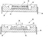
- FIG. 1Ashows a schematic cross-section view of a first example, according to the present invention, of a microelectronic device 10 with a sensitive area 12 .
- microelectronic device 10can include an airbag accelerometer, a microengine, an optical switch, a gyroscopic device, a microsensor, and a microactuator.
- Microelectronic device 10can include microelectromechanical systems (MEMS) that have MEMS elements (e.g. gears, hinges, levers, slides, and mirrors). These free-standing MEMS elements must be free to move, rotate, etc during MEMS operation.
- MEMSmicroelectromechanical systems
- Microelectronic device 10can also include IMEMS devices, which combine integrated circuits (IC's), such as CMOS or Bipolar circuits, with MEMS devices on a single substrate, such as a multi-chip module (MCM).
- IMEMS deviceswhich combine integrated circuits (IC's), such as CMOS or Bipolar circuits, with MEMS devices on a single substrate, such as a multi-chip module (MCM).
- MCMmulti-chip module
- Microelectronics device 10can also include microsensors, which must be freely-exposed to the environment during operation (e.g. for chemical, pressure, or temperature measurements).
- Microelectronics device 10can also include microfluidic systems, such as used in Chemical-Lab-on-a-Chip systems.
- FIG. 1Bshows a schematic cross-section view of a first example, according to the present invention, that is similar to FIG. 1A, after a water-insoluble protective coating 14 has been applied to the sensitive area 12 .
- the application of protective coating 14can potentially prevent damage due to external contamination, debris, moisture, cutting fluids, handling forces, electrostatic effects, etc.
- Sensitive area 12can include a released MEMS element, an IC, an optically active surface, a chemically-sensitive surface, a pressure-sensitive surface, or a temperature-sensitive surface.
- optically active devicesinclude charge coupled devices (CCD), photocells, laser diodes, vertical cavity surface emitting lasers (VCSEL's), and UV erasable programmable read-only memory chips (UV-EPROM's). While some of these devices emit light, and while others receive light; both are considered to be “optically active”.
- the ideal protective coating 14would be water-insoluble, vacuum vapor-deposited, strong, pure, inert, defect-free, dry-etchable, and conformal. Coatings made from parylene generally satisfy these requirements.
- Other suitable protective coatingscan include silicon nitride, metal (e.g. aluminum or tungsten), a vapor deposited organic material, cynoacrylate, a carbon film, a self-assembled monolayered material, perfluoropolyether, hexamethyidisilazane, or perfluorodecanoic carboxylic acid, silicon dioxide, silicate glass, or combinations thereof.
- Other glass formulationse.g.
- boron or phosphorouscan be used which have the desirable property of being more rapidly etched (e.g. fast-etch glass), even though other properties (e.g. dielectric strength) may not be as good as compared to pure silicon dioxide.
- amorphous carbon films, or diamond-like carbon films (DLC)can be used.
- the preferred water-insoluble protective coating 14is a material chosen from the family of vacuum vapor-deposited (e.g. CVD or PECVD) materials called “parylene”.
- Other polymer coatingscould be used, for example: epoxies, acrylics, urethanes, and silicones. However, those other coatings are generally applied in the liquid state, whereas parylene is applied in the vapor-phase. Liquid coatings generally do not conform as well to the complex 3-D shaped, multi-layer MEMS elements as vacuum vapor-deposited conformal coatings, such as parylene.
- Paryleneis the generic name for members of a unique polymer series originally developed by the Union Carbide Corporation.
- the basic member of the seriesis poly-para-xylylene; a completely linear, highly crystalline material called Parylene N.
- Parylene Nis a primary dielectric, exhibiting a very low dissipation factor, high dielectric strength, and a dielectric constant invariant with frequency.
- Parylene Cthe second commercially available member of the Union Carbide series, is produced from the same monomer, which has been modified by the substitution of a chlorine atom for one of the aromatic hydrogens. Parylene C has passed the NASA Goddard Space Flight Center outgassing test.
- Parylene Chas a useful combination of electrical and physical properties plus a very low permeability to moisture and other corrosive gases. It also has the ability to provide a true pinhole-free conformal insulation. For these reasons, Parylene C is a preferred material for coating critical electronic assemblies.
- Parylene Dthe third member of the Union Carbide series, is produced from the same monomer, but modified by the substitution of the chlorine atom for two of the aromatic hydrogens. Parylene D has similar properties to Parylene C, but with the ability to withstand higher use temperatures. Due to the uniqueness of the vapor phase deposition, the parylene family of polymers can be formed as structurally continuous films as thin as a fraction of a micrometer, to as thick as several thousandths of an inch.
- Vacuum vapor-deposited parylene coatings 14are applied to specimens in an evacuated deposition chamber by means of gas phase polymerization.
- the parylene raw material, di-para-xylylene dimeris a white crystalline powder manufactured by Union Carbide Corporation, Danbury, Conn. under the product name “Parylene Dimer DPX-N”.
- the powderis vaporized at approximately 150 degrees C.
- itis molecularly cleaved (e.g. pyrolyzed) in a second process at about 680 degrees C. to form the diradical, para-xylylene, which is then introduced as a monomeric gas that polymerizes on the specimens in the vacuum chamber at room temperature.
- the coatinggrows as a pure, defect-free, self-assembling, conformal film on all exposed surfaces, edges, and crevices.
- the active (cured) monomeric gaspolymerizes spontaneously on the surface of coated specimen at ambient temperature with no stresses induced initially or subsequently. In short, there are no cure-related hydraulic or liquid surface tension forces in the process. Parylenes are formed at a vacuum of approximately 0.1 torr, and under these conditions the mean-free-path of the gas molecules in the deposition chamber is in the order of 0.1 cm. In the free molecular dispersion of the vacuum environment, all sides of an object to be coated are uniformly impinged by the gaseous monomer, resulting in a high degree of conformity. Polymerization occurs in crevices, under devices, and on exposed surfaces at the same rate of about 0.2 microns per minute for Parylene C, and a somewhat slower rate for parylene N. The deposition rate depends strongly on processing conditions.
- Parylenepossesses useful dielectric and barrier properties per unit thickness, as well as extreme chemical inertness and freedom from pinholes. Since parylene is non-liquid, it does not pool, bridge, or exhibit meniscus or capillary properties during application. No catalysts or solvents are involved, and no foreign substances are introduced that could contaminate coated specimens. Parylene thickness is related to the amount of vaporized dimer and dwell time in the vacuum chamber, and can be controlled accurately to +/ ⁇ 5% of final thickness. The vacuum deposition process makes parylene coating relatively simple to control, as opposed to liquid materials, where neither thickness nor evenness can be accurately controlled. Parylene film meets typical printed wiring assembly coating protection and electrical insulating standards; as specified by MIL-I-46058. The coating's thickness is controllable from as little as 100 Angstroms, to hundreds of microns.
- parylene polymer coatingshave fairly good adhesion to epoxy molding compounds.
- parylene monomeris soluble in epoxy gel-coat.
- parylene polymeris formed under the surface of the epoxy, resulting in an interpenetrating polymer network and an especially effective mechanism for adhesion, if required.
- Parylene polymersresist attack and are insoluble in all organic solvents up to 150 C, including water. Parylene C can be dissolved in chloro-naphthalene at 175 C, and Parylene N is soluble at the solvent's boiling point of 265 C. Parylene coatings can be removed by many processes, including oxygen or ozone reactive ion plasma exposure; and laser ablation. Oxygen-based plasma exposure does not harm the polysilicon structural elements of MEMS devices. Dry etching of parylene coatings is generally faster than dry etching of silicon dioxide glass coatings, which supports the preferred choice of parylene for use as the protective coating 14 , as compared to using silicon dioxide glass.
- Reactive parylene monomerscan be blended with other reactive materials to form copolymer compounds, including silicon, carbon, and fluorine containing monomers (including siloxanes). Additional information on the formation and composition of thin parylene films on semiconductor substrates for use as a low-dielectric, insulating coating is contained in U.S. Pat. No. 5,958,510 to Sivaramakrishnam, et al., and in U.S. Pat. No. 6,030,706, to Eissa, et al. Both patents are herein incorporated by reference in their entirety.
- FIG. 1Cshows a schematic cross-section view of a first example, according to the present invention, that is similar to FIG. 1B, after device 10 has been conventionally attached to substrate 16 , and electrically interconnected to substrate 16 with wirebonds 18 .
- Other packaging stepswell-known to those skilled in the art, could be performed at this stage, such as encasing the wirebonds in a plastic material (not shown).
- Protective coating 14protects sensitive area 12 during these packaging steps.
- FIG. 1Dshows a schematic cross-section view of a first example, according to the present invention, that is similar to FIG. 1C, after protective coating 14 has been substantially removed by using an etching process 20 , thereby exposing sensitive area 12 to the surrounding environment.
- etching solutionscan be used to chemically remove coatings.
- Wet etching of silicon dioxide or silicate glasscan use hydrofluoric or hydrochloric acid, followed by rinsing, and drying. Drying can include using supercritical drying and sublimation methods to reduce stiction problems.
- Etching solutions for removing plastic materialse.g. epoxy resin and glob-top polymers
- etchingcan be performed with a commercially available device conventionally called a “decapsulator”, or “jet etcher”. such a device removes material by directing a stream of (sometimes heated) acid etchant perpendicular to the surface being etched. A gasket can be used to confine the area being etched. The etching solutions can be heated to 250 C, and +/ ⁇ 1% temperature control is provided.
- a decapsulator deviceis the “D Cap-Delta” dual acid system sold by B&G International, Santa Crux, Calif., 95060.
- Other decapsulating devicesare also described in U.S. Pat. No. 5,855,727 to Martin, et al.; and in U.S. Pat. No. 5,932,061 to Lam.
- dry plasma etchingcan be used to substantially remove protective coating 14 , instead of wet etching. Dry etching processes are generally less damaging to the fragile MEMS elements than wet processes. Plasma etching can include reactive ion etching and ion milling with chemically active ions (e.g. oxygen, chlorine, or fluorine ions). Exposure to ozone in the presence of UV radiation can also be used for dry etching. It is critical that the release process does not substantially damage other features on the microelectronic device, such as metal interconnects.
- Another dry etching processis exposure to gas or gases.
- gas or gasesFor example, chlorine gas can be used to etch a tungsten protective coating, and xenon diflouride can be used to etch silicon.
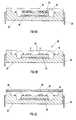
- FIG. 2Ashows a schematic cross-section view of a second example, according to the present invention, of a wafer 22 with a plurality of already released MEMS elements 24 located on the wafer 22 .
- FIG. 2Bshows a schematic cross-section view of a second example, according to the present invention, that is similar to FIG. 2A, after an optional anti-stiction coating 26 has been applied to the released MEMS elements 24 .
- a schematic MEMS device 40is shown, having MEMS elements 24 comprising two polysilicon gears 42 , 44 and a linkage bar 46 .
- Anti-stiction coating 26 in FIG. 2Bis an example of a class of performance-enhancing and/or proprietary films that can be applied to released MEMS elements 24 . Examples of performance-enhancing films include anti-stiction films, adhesion-inhibitors, lubricants (e.g.
- FIG. 2Cshows a schematic cross-section view of a second example, according to the present invention, that is similar to FIG. 2B, after water-insoluble protective coating 14 has been applied to the released MEMS elements 24 , on top of the antistiction coating of FIG. 2 B.
- Protective coating 14substantially encapsulates the released MEMS elements 24 , thereby inactivating them and protecting them with a durable coating.
- Coating 14can be a vacuum vapor-deposited parylene coating. Coating 14 can be applied to the entire topside of wafer 22 without the need for masking or patterning. However, the backside of wafer 22 may be covered to prevent unwanted deposition thereon of coating 14 .
- Preparation of the wafer's backsidecan include cleaning of unintentionally-deposited materials on the wafer's backside (such as anti-stiction films or MEMS lubricants); removing the native oxide film; and/or deposition of adhesion-enhancing layers to the backside, such as gold. Since MEMS elements 24 are stabilized and protected by protective coating 14 , these optional backside preparation steps can be performed using conventional techniques, and without a requirement for extraordinary care.
- FIG. 2Dshows a schematic cross-section view of a second example, according to the present invention, that is similar to FIG. 2C, after bond pads 29 have been optionally exposed by machining vias 27 in the coatings.
- Vias 27can be defined by photolithography, and can be fabricated by using processes well-known in the art (e.g. e-beam ablation, laser ablation, and water-jet cutting).
- FIG. 2Eshows a schematic cross-section view of a second example, according to the present invention, that is similar to FIG. 2D, wherein wafer 22 is being cut into individual device dies 28 by using processes well-known in the art (e.g. diamond saw cutting, water-jet cutting, and laser dicing).
- MEMS elements 24are protected by coating 14 from damage from cutting debris and lubricant fluids that are typically used during wafer dicing.
- protective coating 14could be patterned in a manner to exclude coating 14 from the wafer saw streets (e.g. lines where the saw cuts along), prior to saw cutting. This would be desirable to avoid contaminating the dicing saw with unwanted debris (e.g. organic debris) generated by cutting of coating 14 .
- Exclusion of coating 14 from the wafer saw streetscan be accomplished by masking during deposition of the coating.
- the coatingcan be removed from the wafer's saw streets by wet or dry etching using a patterned mask.
- An optional cleaning stepcan be performed after dicing wafer 22 .
- FIG. 2Fshows a schematic cross-section view of a second example, according to the present invention, that is similar to FIG. 2E, wherein protective coating 14 is being substantially removed by etching process 20 , thereby re-releasing the MEMS element 24 , and producing a released MEMS device die 30 . It is important that the etching process 20 does not also remove any performance-enhancing coatings, such as anti-stiction coating 26 . Optional probe testing of each MEMS or IMEMS device die 30 can be performed at this stage to determine which ones are the “good” dies; since the released MEMS elements 24 are free and fully functional.
- FIG. 3Ashows a schematic cross-section view of a third example, according to the present invention, of a microelectronic device 10 attached and wirebonded to a package 32 , with MEMS elements 24 protected in a protective coating 14 .
- Package 32has exterior electrical leads 34 .
- Other interconnection methodssuch as flip-chip solder bumps, or direct metallization, can be used in place of wirebonds.
- the use of protective coating 14 to encapsulate MEMS elements 24permits a wide range of die attach processes and materials to be used without fear of adsorption of potentially harmful layers on the MEMS elements.
- Use of protective coating 14also allows ultrasonic wirebonding or other interconnection steps to occur without damage due to mechanical vibrations or shock to the MEMS devices.
- FIG. 3Bshows a schematic cross-section view of a third example, according to the present invention, that is similar to FIG. 3A, wherein the protective coating 14 is substantially removed by a dry oxygen plasma etching process 20 , thereby re-releasing the MEMS elements 24 .
- the protective coating 14can be only partially removed, whereby some residual amount of protective coating 14 remains. While sufficient amount of coating 14 must be removed so that MEMS element 24 is released, there are three reasons for not completely removing protective coating 14 . Firstly, it might not be desirable to remove the performance-enhancing films 26 (e.g. anti-stiction and lubricants) applied previously. This can be prevented by not removing all of protective coating 14 . Secondly, leaving a thin layer of protective coating 14 in place may be desirable if coating 14 can act as its own lubricant. This second option could possibly eliminate the extra step of applying performance-enhancing films 26 in FIG. 2 B. Thirdly, leaving a thin layer of coating 14 can possibly reduce micromachining tolerances between bearing surfaces, whereby wobble in gears and discs can be reduced, for example.
- the performance-enhancing films 26e.g. anti-stiction and lubricants
- FIG. 3Cshows a schematic cross-section view of a third example, according to the present invention, that is similar to FIG. 3B, wherein a cover lid 36 has been attached to the package 32 , thereby completing the packaging of the released MEMS device 30 .
- Cover lid 36can optionally include a window 38 , for providing optical access to MEMS device 30 .
- Optical access to operational MEMS devicescan be useful for calibration, inspection, performance characterization, and failure analysis of MEMS elements.
Landscapes
- Engineering & Computer Science (AREA)
- Microelectronics & Electronic Packaging (AREA)
- Manufacturing & Machinery (AREA)
- Physics & Mathematics (AREA)
- Condensed Matter Physics & Semiconductors (AREA)
- General Physics & Mathematics (AREA)
- Computer Hardware Design (AREA)
- Power Engineering (AREA)
- Micromachines (AREA)
- Dicing (AREA)
Abstract
Description
The United States Government has rights in this invention pursuant to Department of Energy Contract No. DE-AC04-94AL85000 with Sandia Corporation.
None applicable
This invention relates generally to the field of microelectronics and more specifically to packaging of microelectromechanical systems (MEMS) and integrated microelectromechanical systems (IMEMS) devices.
Examples of MEMS and IMEMS devices include airbag accelerometers, microengines, optical switches, gyroscopic devices, sensors, and actuators. IMEMS devices can combine integrated circuits (IC's), such as CMOS or Bipolar circuits, with the MEMS devices on a single substrate, such as a multi-chip module (MCM). All of these devices use active elements (e.g. gears, hinges, levers, slides, and mirrors). These freestanding structures must be free to move, rotate, etc. Additionally, some types of microelectronics devices, such as microsensors, must be freely exposed to the environment during operation (e.g. for chemical, pressure, or temperature measurements).
For current commercially packaged MEMS and IMEMS components, the steps of packaging and testing can account for at least 70% of the cost. The current low-yield of MEMS packaging is a “show-stopper” for the eventual success of MEMS. Conventional electronic packaging methods, although expensive, are not presently adequate to carry these designs to useful applications with acceptable yields and reliability.
During conventional MEMS fabrication, silicon dioxide or silicate glass is a sacrificial material commonly used at the wafer scale to enable creation of complex three-dimensional structural shapes from polycrystalline silicon (e.g. polysilicon). The glass sacrificial layer surrounds and covers the multiple layers of polysilicon MEMS elements, preventing them from moving freely during fabrication. At this stage, the MEMS elements are referred to as being “unreleased”.
The next step is to “release” and make free the MEMS elements. Conventionally, this is done by dissolving or etching the glass sacrificial coating in liquid mixtures of hydrofluoric acid, hydrochloric acid, or combinations of the two acids. This wet etching step is typically done at the wafer scale in order to reduce processing costs. Alternatively, a dry release etch may be performed by exposing the wafer to a plasma containing reactive oxygen, chlorine, or fluorine ions. Herein, the word “wafer” can include silicon; gallium arsinide (GaAs); or quartz wafers or substrates (e.g. for MEMS structures).
After releasing the active elements, the MEMS devices can be probed to test their functionality. Unfortunately, probed “good” MEMS are then lost in significant quantity due to damage during subsequent packaging steps. They can be damaged because they are unprotected (e.g. released). Subsequent processing steps can include sawing or cutting (e.g. dicing) the wafer into individual chips or device dies (e.g. dicing); attaching the device to the package (e.g. die attach), wirebonding or other interconnection methods, such as flip-chip solder bumping, or direct metallization (e.g. interconnecting); pre-seal inspection; sealing of hermetic or dust protection lids; windowing; package sealing; plating; trim; marking; final test; shipping; storage; and installation. Potential risks to the delicate released MEMS elements include electrostatic effects, dust, moisture, contamination, handling stresses, and thermal effects. For example, ultrasonic bonding of wirebond joints can impart harmful vibrations to the fragile released MEMS elements.
One solution to this problem is to keep the original sacrificial glass coating intact for as long as possible. In one approach, the MEMS elements would be released after all of the high-risk packaging steps have been completed (including sawing of the wafer into chips). Another approach (which relates to the present invention) would be to release the MEMS elements at the wafer scale; apply any performance-enhancing coatings; re-apply a temporary, replacement protective coating prior to wafer sawing; and, finally, remove the protective coating after all of the high-risk packaging steps have been completed.
In order to reduce the costs of MEMS fabrication and packaging, it is desirable to perform as many fabrication steps at the wafer scale (e.g. before sawing the wafer into individual device dies). An example of a wafer scale process is deposition of performance-enhancing coatings on released MEMS elements (e.g. anti-stiction films and adhesion-inhibitors). Unfortunately, if these coatings are applied at the wafer scale (obviously, on released MEMS elements), then some of these performance-enhancing coatings may also be unintentionally deposited on the backside of the wafer. These unwanted coatings can interfere with the subsequent die attachment step. Also, the subsequent removal of these unwanted backside coatings can damage or contaminate the released MEMS elements.
Likewise, application of adhesion-promoting coatings (e.g. for die attachment) to the backside of the wafer may similarly damage the released MEMS elements by unintentional contamination or adsorption of harmful materials.
What is desired is a process that first releases the MEMS elements at the wafer scale; then applies all of the desired performance-enhancing coatings to the released MEMS elements; followed by re-application of a temporary protective coating; followed by cleanup of unwanted coatings unintentionally applied to the wafer's backside, followed by cutting the wafer into individual device dies.
Another desirable goal is to replace conventional wet etching processes with dry etching processes; to reduce costs, and because of an increasing emphasis on using environmentally friendly fabrication and cleaning processes. Especially for IMEMS devices, which can contain CMOS or Bipolar structures and other semiconductor materials, aggressive wet etchants used to release MEMS elements can damage the CMOS or Bipolar structures if they are not sufficiently protected. Standard photoresist protection used on CMOS or Bipolar chips may not provide sufficient protection from attack by acid etchants.
Wet etching processes can have other problems. Large hydrodynamic forces may be unintentionally applied to the fragile released MEMS elements, such as when agitating within a bath, and can fracture thin elements. Also, improper removal of any liquid film can create stiction problems resulting from capillary effects during the process of immersion in, removal from, and drying of liquid solutions. Using dry processing can eliminate these potential sources of damage.
What is also desired is using a dry etching process, preferably single-step, for removing protective coatings from MEMS devices. It is also desired that the dry etching process can be stopped before completely removing all of the protective coating, thereby leaving some desirable residual material that may reduce friction and may reduce tolerances between bearing surfaces, potentially reducing wobble in rotating gears and discs.
The list of desired objects described above could apply to microelectronics devices other than MEMS or IMEMS, such as microsensors. Microsensors also have a need for temporary protection of sensitive areas during packaging steps.
None of the approaches discussed above provides a low-cost, high-yield, high-capacity commercial wafer-scale, water-insoluble, protection film or coating that provides MEMS and IMEMS stabilization and protection during device packaging.
Use of the word “MEMS” is intended to also include “IMEMS” devices, unless specifically stated otherwise. Likewise, the word “plastic” is intended to include any type of flowable dielectric composition. The word “film” is used interchangeably with “coating”, unless otherwise stated. The phrases “released MEMS elements”, “released MEMS elements”, “sensitive area”, and “active MEMS elements” are used interchangeably to refer to the freely-movable structural elements, such as gears, pivots, hinges, sliders, etc.; and also to exposed active elements (e.g. flexible membranes) for microsensors (e.g. chemical, pressure, and temperature microsensors).
The accompanying drawings, which are incorporated in and form part of the specification, illustrate various embodiments of the present invention and, together with the description, serve to explain the principles of the invention.
FIG. 1A shows a schematic cross-section view of a first example, according to the present invention, of a microelectronic device with a sensitive area.
FIG. 1B shows a schematic cross-section view of a first example, according to the present invention, that is similar to FIG. 1A, after a water-insoluble protective coating has been applied to the sensitive area.
FIG. 1C shows a schematic cross-section view of a first example, according to the present invention, that is similar to FIG. 1B, after the device has been attached and wirebonded to a substrate.
FIG. 1D shows a schematic cross-section view of a first example, according to the present invention, that is similar to FIG. 1C, after the protective coating has been removed by etching, thereby exposing the sensitive area to the surrounding environment.
FIG. 2A shows a schematic cross-section view of a second example, according to the present invention, of a wafer substrate with already released MEMS elements located on the wafer's topside.
FIG. 2B shows a schematic cross-section view of a second example, according to the present invention, that is similar to FIG. 2A, after an anti-stiction coating has been applied to the released MEMS elements.
FIG. 2C shows a schematic cross-section view of a second example, according to the present invention, that is similar to FIG. 2B, after a water-insoluble protective coating has been applied to the released MEMS elements, on top of the antistiction coating of FIG.2B. The coating can be a vacuum vapor deposited parylene coating.
FIG. 2D shows a schematic cross-section view of a second example, according to the present invention, that is similar to FIG. 2C, after bond pads have been exposed by machining vias in the coatings.
FIG. 2E shows a schematic cross-section view of a second example, according to the present invention, that is similar to FIG. 2D, wherein the wafer is being cut into individual device dies by diamond saw cutting or laser dicing.
FIG. 2F shows a schematic cross-section view of a second example, according to the present invention, that is similar to FIG. 2E, wherein the protective coating is being removed by etching, thereby re-releasing the MEMS elements.
FIG. 3A shows a schematic cross-section view of a third example, according to the present invention, of a MEMS device attached and wirebonded to a package, with MEMS elements protected in a protective coating.
FIG. 3B shows a schematic cross-section view of a third example, according to the present invention, that is similar to FIG. 3A, wherein the protective coating is being removed by dry oxygen plasma etching, thereby re-releasing the MEMS elements.
FIG. 3C shows a schematic cross-section view of a third example, according to the present invention, that is similar to FIG. 3B, wherein a cover lid with a window has been attached to the package, thereby completing the packaging of the released MEMS device.
The present invention relates to a method of protecting a microelectronic device during device packaging, comprising, in the order presented: providing a microelectronic device having a sensitive area; applying a water-insoluble, protective coating to the sensitive area; performing at least one packaging step; and then substantially removing the protective coating from the sensitive area.
FIG. 1A shows a schematic cross-section view of a first example, according to the present invention, of amicroelectronic device 10 with asensitive area 12. Examples ofmicroelectronic device 10 can include an airbag accelerometer, a microengine, an optical switch, a gyroscopic device, a microsensor, and a microactuator.Microelectronic device 10 can include microelectromechanical systems (MEMS) that have MEMS elements (e.g. gears, hinges, levers, slides, and mirrors). These free-standing MEMS elements must be free to move, rotate, etc during MEMS operation.Microelectronic device 10 can also include IMEMS devices, which combine integrated circuits (IC's), such as CMOS or Bipolar circuits, with MEMS devices on a single substrate, such as a multi-chip module (MCM).Microelectronics device 10 can also include microsensors, which must be freely-exposed to the environment during operation (e.g. for chemical, pressure, or temperature measurements).Microelectronics device 10 can also include microfluidic systems, such as used in Chemical-Lab-on-a-Chip systems.
FIG. 1B shows a schematic cross-section view of a first example, according to the present invention, that is similar to FIG. 1A, after a water-insolubleprotective coating 14 has been applied to thesensitive area 12. The application ofprotective coating 14 can potentially prevent damage due to external contamination, debris, moisture, cutting fluids, handling forces, electrostatic effects, etc.Sensitive area 12 can include a released MEMS element, an IC, an optically active surface, a chemically-sensitive surface, a pressure-sensitive surface, or a temperature-sensitive surface. Examples of optically active devices include charge coupled devices (CCD), photocells, laser diodes, vertical cavity surface emitting lasers (VCSEL's), and UV erasable programmable read-only memory chips (UV-EPROM's). While some of these devices emit light, and while others receive light; both are considered to be “optically active”.
The idealprotective coating 14 would be water-insoluble, vacuum vapor-deposited, strong, pure, inert, defect-free, dry-etchable, and conformal. Coatings made from parylene generally satisfy these requirements. Other suitable protective coatings can include silicon nitride, metal (e.g. aluminum or tungsten), a vapor deposited organic material, cynoacrylate, a carbon film, a self-assembled monolayered material, perfluoropolyether, hexamethyidisilazane, or perfluorodecanoic carboxylic acid, silicon dioxide, silicate glass, or combinations thereof. Other glass formulations (e.g. containing boron or phosphorous)can be used which have the desirable property of being more rapidly etched (e.g. fast-etch glass), even though other properties (e.g. dielectric strength) may not be as good as compared to pure silicon dioxide. Alternatively, amorphous carbon films, or diamond-like carbon films (DLC) can be used.
The preferred water-insolubleprotective coating 14 is a material chosen from the family of vacuum vapor-deposited (e.g. CVD or PECVD) materials called “parylene”. Other polymer coatings could be used, for example: epoxies, acrylics, urethanes, and silicones. However, those other coatings are generally applied in the liquid state, whereas parylene is applied in the vapor-phase. Liquid coatings generally do not conform as well to the complex 3-D shaped, multi-layer MEMS elements as vacuum vapor-deposited conformal coatings, such as parylene.
Parylene is the generic name for members of a unique polymer series originally developed by the Union Carbide Corporation. The basic member of the series is poly-para-xylylene; a completely linear, highly crystalline material called Parylene N. Parylene N is a primary dielectric, exhibiting a very low dissipation factor, high dielectric strength, and a dielectric constant invariant with frequency. Parylene C, the second commercially available member of the Union Carbide series, is produced from the same monomer, which has been modified by the substitution of a chlorine atom for one of the aromatic hydrogens. Parylene C has passed the NASA Goddard Space Flight Center outgassing test. Parylene C has a useful combination of electrical and physical properties plus a very low permeability to moisture and other corrosive gases. It also has the ability to provide a true pinhole-free conformal insulation. For these reasons, Parylene C is a preferred material for coating critical electronic assemblies.
Parylene D, the third member of the Union Carbide series, is produced from the same monomer, but modified by the substitution of the chlorine atom for two of the aromatic hydrogens. Parylene D has similar properties to Parylene C, but with the ability to withstand higher use temperatures. Due to the uniqueness of the vapor phase deposition, the parylene family of polymers can be formed as structurally continuous films as thin as a fraction of a micrometer, to as thick as several thousandths of an inch.
Vacuum vapor-depositedparylene coatings 14 are applied to specimens in an evacuated deposition chamber by means of gas phase polymerization. The parylene raw material, di-para-xylylene dimer, is a white crystalline powder manufactured by Union Carbide Corporation, Danbury, Conn. under the product name “Parylene Dimer DPX-N”. First, the powder is vaporized at approximately 150 degrees C. Then it is molecularly cleaved (e.g. pyrolyzed) in a second process at about 680 degrees C. to form the diradical, para-xylylene, which is then introduced as a monomeric gas that polymerizes on the specimens in the vacuum chamber at room temperature. There is no liquid phase in the deposition process, and specimen temperatures remain near ambient. The coating grows as a pure, defect-free, self-assembling, conformal film on all exposed surfaces, edges, and crevices.
During the deposition stage, the active (cured) monomeric gas polymerizes spontaneously on the surface of coated specimen at ambient temperature with no stresses induced initially or subsequently. In short, there are no cure-related hydraulic or liquid surface tension forces in the process. Parylenes are formed at a vacuum of approximately 0.1 torr, and under these conditions the mean-free-path of the gas molecules in the deposition chamber is in the order of 0.1 cm. In the free molecular dispersion of the vacuum environment, all sides of an object to be coated are uniformly impinged by the gaseous monomer, resulting in a high degree of conformity. Polymerization occurs in crevices, under devices, and on exposed surfaces at the same rate of about 0.2 microns per minute for Parylene C, and a somewhat slower rate for parylene N. The deposition rate depends strongly on processing conditions.
Parylene possesses useful dielectric and barrier properties per unit thickness, as well as extreme chemical inertness and freedom from pinholes. Since parylene is non-liquid, it does not pool, bridge, or exhibit meniscus or capillary properties during application. No catalysts or solvents are involved, and no foreign substances are introduced that could contaminate coated specimens. Parylene thickness is related to the amount of vaporized dimer and dwell time in the vacuum chamber, and can be controlled accurately to +/−5% of final thickness. The vacuum deposition process makes parylene coating relatively simple to control, as opposed to liquid materials, where neither thickness nor evenness can be accurately controlled. Parylene film meets typical printed wiring assembly coating protection and electrical insulating standards; as specified by MIL-I-46058. The coating's thickness is controllable from as little as 100 Angstroms, to hundreds of microns.
The parylene polymer coatings have fairly good adhesion to epoxy molding compounds. Interestingly, parylene monomer is soluble in epoxy gel-coat. Here, parylene polymer is formed under the surface of the epoxy, resulting in an interpenetrating polymer network and an especially effective mechanism for adhesion, if required.
Curing occurs during deposition; therefore no high temperature curing step is required. Since parylene is applied in a non-liquid state, there are no hydrodynamic forces that could damage the fragile released MEMS elements. Deposition also takes place at ambient temperatures, which minimize thermal or chemical cure stresses. Parylene's static and dynamic coefficients of friction are in the range of 0.25 to 0.33 (in air), which makes this coating only slightly less lubricious than TEFLON. Because the parylene deposition process is spontaneous, and does not require a cure catalyst, it is therefore extremely pure and chemically inert.
Parylene polymers resist attack and are insoluble in all organic solvents up to 150 C, including water. Parylene C can be dissolved in chloro-naphthalene at 175 C, and Parylene N is soluble at the solvent's boiling point of 265 C. Parylene coatings can be removed by many processes, including oxygen or ozone reactive ion plasma exposure; and laser ablation. Oxygen-based plasma exposure does not harm the polysilicon structural elements of MEMS devices. Dry etching of parylene coatings is generally faster than dry etching of silicon dioxide glass coatings, which supports the preferred choice of parylene for use as theprotective coating 14, as compared to using silicon dioxide glass.
Reactive parylene monomers can be blended with other reactive materials to form copolymer compounds, including silicon, carbon, and fluorine containing monomers (including siloxanes). Additional information on the formation and composition of thin parylene films on semiconductor substrates for use as a low-dielectric, insulating coating is contained in U.S. Pat. No. 5,958,510 to Sivaramakrishnam, et al., and in U.S. Pat. No. 6,030,706, to Eissa, et al. Both patents are herein incorporated by reference in their entirety.
FIG. 1C shows a schematic cross-section view of a first example, according to the present invention, that is similar to FIG. 1B, afterdevice 10 has been conventionally attached tosubstrate 16, and electrically interconnected tosubstrate 16 withwirebonds 18. Other packaging steps, well-known to those skilled in the art, could be performed at this stage, such as encasing the wirebonds in a plastic material (not shown).Protective coating 14 protectssensitive area 12 during these packaging steps.
FIG. 1D shows a schematic cross-section view of a first example, according to the present invention, that is similar to FIG. 1C, afterprotective coating 14 has been substantially removed by using anetching process 20, thereby exposingsensitive area 12 to the surrounding environment.
A variety of etching solutions can be used to chemically remove coatings. Wet etching of silicon dioxide or silicate glass can use hydrofluoric or hydrochloric acid, followed by rinsing, and drying. Drying can include using supercritical drying and sublimation methods to reduce stiction problems. Etching solutions for removing plastic materials (e.g. epoxy resin and glob-top polymers) can include using fuming nitric acid, fuming sulfuric acid, or mixtures of the two acids.
Wet etching can be performed with a commercially available device conventionally called a “decapsulator”, or “jet etcher”. such a device removes material by directing a stream of (sometimes heated) acid etchant perpendicular to the surface being etched. A gasket can be used to confine the area being etched. The etching solutions can be heated to 250 C, and +/−1% temperature control is provided. An example of a decapsulator device is the “D Cap-Delta” dual acid system sold by B&G International, Santa Crux, Calif., 95060. Other decapsulating devices are also described in U.S. Pat. No. 5,855,727 to Martin, et al.; and in U.S. Pat. No. 5,932,061 to Lam.
Alternatively, dry plasma etching can be used to substantially removeprotective coating 14, instead of wet etching. Dry etching processes are generally less damaging to the fragile MEMS elements than wet processes. Plasma etching can include reactive ion etching and ion milling with chemically active ions (e.g. oxygen, chlorine, or fluorine ions). Exposure to ozone in the presence of UV radiation can also be used for dry etching. It is critical that the release process does not substantially damage other features on the microelectronic device, such as metal interconnects.
Another dry etching process is exposure to gas or gases. For example, chlorine gas can be used to etch a tungsten protective coating, and xenon diflouride can be used to etch silicon.
FIG. 2A shows a schematic cross-section view of a second example, according to the present invention, of awafer 22 with a plurality of already releasedMEMS elements 24 located on thewafer 22.
FIG. 2B shows a schematic cross-section view of a second example, according to the present invention, that is similar to FIG. 2A, after anoptional anti-stiction coating 26 has been applied to the releasedMEMS elements 24. Aschematic MEMS device 40 is shown, havingMEMS elements 24 comprising two polysilicon gears42,44 and alinkage bar 46.Anti-stiction coating 26 in FIG. 2B is an example of a class of performance-enhancing and/or proprietary films that can be applied to releasedMEMS elements 24. Examples of performance-enhancing films include anti-stiction films, adhesion-inhibitors, lubricants (e.g. perfluoropolyether, hexamethyldisilazane, or perfluorodecanoic carboxylic acid), and nitrided-surfaces that reduce friction between moving (e.g. polysilicon) surfaces. In U.S. Pat. No. 5,766,367, “Method for Preventing Micromechanical Structures from Adhering to Another Object”, Smith, et al. discloses the formation of a adhesion-inhibiting hydrophilic coating by immersing the MEMS components in a solvent containing hexamethyldisilazane. U.S. Pat. No. 5,766,367 is herein incorporated by reference in its entirety. Also, vapor-deposited, self-assembling monolayer (SAM) lubricants, such as perfluorodecanoic carboxylic acid, can be used. Finally, some degree of humidity can also help to increase lubricity.
FIG. 2C shows a schematic cross-section view of a second example, according to the present invention, that is similar to FIG. 2B, after water-insolubleprotective coating 14 has been applied to the releasedMEMS elements 24, on top of the antistiction coating of FIG.2B.Protective coating 14 substantially encapsulates the releasedMEMS elements 24, thereby inactivating them and protecting them with a durable coating.Coating 14 can be a vacuum vapor-deposited parylene coating.Coating 14 can be applied to the entire topside ofwafer 22 without the need for masking or patterning. However, the backside ofwafer 22 may be covered to prevent unwanted deposition thereon ofcoating 14. Preparation of the wafer's backside can include cleaning of unintentionally-deposited materials on the wafer's backside (such as anti-stiction films or MEMS lubricants); removing the native oxide film; and/or deposition of adhesion-enhancing layers to the backside, such as gold. SinceMEMS elements 24 are stabilized and protected byprotective coating 14, these optional backside preparation steps can be performed using conventional techniques, and without a requirement for extraordinary care.
FIG. 2D shows a schematic cross-section view of a second example, according to the present invention, that is similar to FIG. 2C, afterbond pads 29 have been optionally exposed by machiningvias 27 in the coatings.Vias 27 can be defined by photolithography, and can be fabricated by using processes well-known in the art (e.g. e-beam ablation, laser ablation, and water-jet cutting).
FIG. 2E shows a schematic cross-section view of a second example, according to the present invention, that is similar to FIG. 2D, whereinwafer 22 is being cut into individual device dies28 by using processes well-known in the art (e.g. diamond saw cutting, water-jet cutting, and laser dicing).MEMS elements 24 are protected by coating14 from damage from cutting debris and lubricant fluids that are typically used during wafer dicing. Alternatively,protective coating 14 could be patterned in a manner to exclude coating14 from the wafer saw streets (e.g. lines where the saw cuts along), prior to saw cutting. This would be desirable to avoid contaminating the dicing saw with unwanted debris (e.g. organic debris) generated by cutting ofcoating 14. Exclusion of coating14 from the wafer saw streets can be accomplished by masking during deposition of the coating. Alternatively, the coating can be removed from the wafer's saw streets by wet or dry etching using a patterned mask. An optional cleaning step can be performed after dicingwafer 22.
FIG. 2F shows a schematic cross-section view of a second example, according to the present invention, that is similar to FIG. 2E, whereinprotective coating 14 is being substantially removed by etchingprocess 20, thereby re-releasing theMEMS element 24, and producing a released MEMS device die30. It is important that theetching process 20 does not also remove any performance-enhancing coatings, such asanti-stiction coating 26. Optional probe testing of each MEMS or IMEMS device die30 can be performed at this stage to determine which ones are the “good” dies; since the releasedMEMS elements 24 are free and fully functional.
FIG. 3A shows a schematic cross-section view of a third example, according to the present invention, of amicroelectronic device 10 attached and wirebonded to apackage 32, withMEMS elements 24 protected in aprotective coating 14.Package 32 has exterior electrical leads34. Other interconnection methods, such as flip-chip solder bumps, or direct metallization, can be used in place of wirebonds. The use ofprotective coating 14 to encapsulateMEMS elements 24 permits a wide range of die attach processes and materials to be used without fear of adsorption of potentially harmful layers on the MEMS elements. Use ofprotective coating 14 also allows ultrasonic wirebonding or other interconnection steps to occur without damage due to mechanical vibrations or shock to the MEMS devices.
FIG. 3B shows a schematic cross-section view of a third example, according to the present invention, that is similar to FIG. 3A, wherein theprotective coating 14 is substantially removed by a dry oxygenplasma etching process 20, thereby re-releasing theMEMS elements 24.
Alternatively, in FIG. 3B, theprotective coating 14 can be only partially removed, whereby some residual amount ofprotective coating 14 remains. While sufficient amount of coating14 must be removed so thatMEMS element 24 is released, there are three reasons for not completely removingprotective coating 14. Firstly, it might not be desirable to remove the performance-enhancing films26 (e.g. anti-stiction and lubricants) applied previously. This can be prevented by not removing all ofprotective coating 14. Secondly, leaving a thin layer ofprotective coating 14 in place may be desirable if coating14 can act as its own lubricant. This second option could possibly eliminate the extra step of applying performance-enhancingfilms 26 in FIG.2B. Thirdly, leaving a thin layer ofcoating 14 can possibly reduce micromachining tolerances between bearing surfaces, whereby wobble in gears and discs can be reduced, for example.
FIG. 3C shows a schematic cross-section view of a third example, according to the present invention, that is similar to FIG. 3B, wherein acover lid 36 has been attached to thepackage 32, thereby completing the packaging of the releasedMEMS device 30.Cover lid 36 can optionally include awindow 38, for providing optical access toMEMS device 30. Optical access to operational MEMS devices can be useful for calibration, inspection, performance characterization, and failure analysis of MEMS elements.
The particular examples discussed above are cited to illustrate particular embodiments of the invention. Other applications and embodiments of the apparatus and method of the present invention will become evident to those skilled in the art. For example, although the figures illustrate only a single microelectronic device or MEMS device, the method described herein applies equally well to packaging of multiple MEMS or IMEMS devices, which can be arrayed in a 1-D or 2-D array. Also, the method of perforating one side of a plastic package can also be applied to an opposite side. One example of this can be perforating both sides of a pressure-sensitive area on a microsensor device that is encapsulated in plastic. By perforating both sides, then a pressure differential can be sensed from one side of the device to the other side. The actual scope of the invention is defined by the claims appended hereto.
Claims (49)
1. A method of protecting a microelectronic device during device packaging, comprising, in the order presented:
providing a microelectronic device having a sensitive area;
vapor depositing a water-insoluble, protective coating on the sensitive area;
performing at least one packaging step; and
substantially removing the protective coating from the sensitive area.
2. The method ofclaim 1 , wherein the active area comprises a released MEMS element.
3. The method ofclaim 2 , whereby removing the protective coating re-releases the MEMS element.
4. The method ofclaim 1 , wherein the microelectronic device is disposed on a wafer.
5. The method ofclaim 4 , wherein said wafer is patterned, whereby said protective coating is substantially removed from the wafer's saw streets before cutting said wafer into individual device dies.
6. The method ofclaim 5 , wherein said wafer is masked during deposition of said protective coating, whereby said coating is substantially not deposited on to the wafer's saw streets, prior to cutting said wafer into individual device dies.
7. The method ofclaim 5 , wherein said protective coating is substantially removed from said saw streets, before cutting said wafer into individual device dies.
8. The method ofclaim 5 , further comprising cutting the wafer into a plurality of individual device dies.
9. The method ofclaim 1 , wherein the step of applying a protective coating comprises vacuum vapor-depositing the coating.
10. The method ofclaim 9 , wherein the vacuum vapor-deposited coating comprises a parylene polymer.
11. The method ofclaim 10 , wherein the parylene coating is selected from the group of parylene polymers consisting of poly-para-xylylene, poly-para-xylylene which has been modified by the substitution of a chlorine atom for one of the aromatic hydrogens, and poly-para-xylylene which has been modified by the substitution of the chlorine atom for two of the aromatic hydrogens.
12. The method ofclaim 10 , further comprising blending the parylene polymer with a reactive material to form a copolymer coating.
13. The method ofclaim 12 , wherein the reactive material comprises a monomer containing an element selected from the group consisting of silicon, carbon, and fluorine, and combinations thereof.
14. The method ofclaim 1 , wherein the protective coating comprises silicon dioxide, silicate glass, or silicon nitride.
15. The method ofclaim 1 , wherein the protective coating comprises a metal.
16. The method ofclaim 15 , wherein the metal comprises aluminum or tungsten.
17. The method ofclaim 1 , wherein the protective coating comprises a vapor deposited organic material.
18. The method ofclaim 1 , wherein the protective coating comprises cynoacrylate.
19. The method ofclaim 1 , wherein the protective coating comprises a carbon film.
20. The method ofclaim 1 , wherein the protective coating comprises a self-assembled monolayered material.
21. The method ofclaim 1 , wherein the protective coating comprises a material selected from the group consisting of perfluoropolyether, hexamethydisilazane, and perfluorodecanoic carboxylic acid.
22. The method ofclaim 1 , further comprising exposing bond pads on the microelectronic device, after applying the protective coating.
23. The method ofclaim 8 , further comprising exposing bond pads on the microelectronic device, after applying the protective coating, but before cutting the wafer.
24. The method ofclaim 1 , wherein the removing step comprises using a dry etching process.
25. The method of24, wherein using the dry etching process comprises exposing the active area to a reactive ion plasma.
26. The method ofclaim 25 , wherein the reactive ion plasma comprises an element selected from the group consisting of oxygen, chlorine, and fluorine, and combinations thereof.
27. A method of packaging a microelectronic device, comprising, in the order presented:
providing a microelectronic device having a sensitive area;
applying a water-insoluble, protective coating to the sensitive area;
providing a package;
attaching the device to the package;
electrically interconnecting the device to the package; and
substantially removing the protective coating from the sensitive area.
28. The method ofclaim 27 , further comprising the step of attaching a cover lid to the package, after substantially removing the protective coating from the active area.
29. The method ofclaim 28 , wherein the cover lid comprises a window.
30. The method ofclaim 27 , wherein the interconnecting step comprises wirebonding.
31. A method of protecting at least one MEMS element during device packaging, comprising, in the order presented:
providing a wafer having a released MEMS element;
applying a performance-enhancing coating to the released MEMS element;
applying a water-insoluble, protective coating on top of the performance-enhancing coating;
cutting the wafer into a plurality of individual device dies; and
removing at least some of the water-insoluble protective coating, while not removing the performance-enhancing coating, whereby some residual amount of protective coating remains.
32. The method ofclaim 31 , wherein all of the protective coating is removed.
33. The method ofclaim 31 , wherein the performance-enhancing coating is selected from the group consisting of an anti-stiction film, an adhesion-inhibiting film, a lubricant, and a nitrided-surface.
34. The method ofclaim 31 , wherein the performance-enhancing coating is selected from the group consisting of perfluoropolyether, hexamethyldisilazane, and perfluorodecanoic carboxylic acid.
35. The method ofclaim 31 , wherein the residual remaining protective coating reduces friction.
36. The method ofclaim 31 , wherein the residual remaining protective coating reduces tolerances between bearing surfaces of the MEMS element.
37. A method of protecting released MEMS elements during wafer dicing, comprising:
providing a wafer comprising a plurality of released MEMS elements fabricated thereon;
vapor depositing a water-insoluble, protective coating on the wafer such that the protective coating covers and encapsulates the released MEMS elements for protection during packaging steps subsequent to dicing; and then
dicing the wafer to form a plurality of individual dies.
38. The method ofclaim 37 , further comprising removing the protective coating after dicing the wafer.
39. The method ofclaim 1 , wherein vapor depositing comprises using a Chemical Vapor Deposition (CVD) process.
40. The method ofclaim 1 , wherein vapor depositing comprises using a Plasma Enhanced Chemical Vapor Deposition (PECVD) process.
41. The method ofclaim 1 , wherein vapor depositing comprises polymerizing a monomeric gas on the surface to be coated.
42. The method ofclaim 1 , wherein the temperature of the sensitive area remains essentially at ambient temperature during vapor depositing.
43. The method ofclaim 24 , wherein the dry etching process comprises exposure to chlorine gas.
44. The method ofclaim 24 , wherein the dry etching process comprises ion milling.
45. The method ofclaim 24 , wherein the dry etching process comprises exposure to ozone in the presence of UV radiation.
46. A method of protecting at least one MEMS element during device packaging, comprising, in the order presented:
providing a wafer having a released MEMS element;
applying a water-insoluble, performance-enhancing coating to the released MEMS element;
applying a water-insoluble, protective coating on top of the performance-enhancing coating;
dicing the wafer into a plurality of individual device dies; and
removing at least some of the protective coating, while not removing the performance-enhancing coating, whereby some residual amount of protective coating remains.
47. A method of protecting at least one MEMS element during device packaging, comprising, in the order presented:
providing a wafer having a released MEMS element;
applying a performance-enhancing coating directly to the released MEMS element;
applying a water-insoluble, protective coating directly on top of the performance-enhancing coating;
cutting the wafer into a plurality of individual device dies; and
removing at least some of the water-insoluble protective coating, while not removing the performance-enhancing coating, whereby some residual amount of protective coating remains.
48. The method ofclaim 1 , wherein the microelectronic device having a sensitive area comprises a wafer having the sensitive area disposed thereon, and further wherein the step of performing at least one packaging step comprises dicing said wafer to form a plurality of individual dies.
49. The method ofclaim 4 , wherein the step of performing at least one packaging step comprises dicing said wafer to form a plurality of individual dies.
Priority Applications (3)
| Application Number | Priority Date | Filing Date | Title |
|---|---|---|---|
| US09/572,562US6335224B1 (en) | 2000-05-16 | 2000-05-16 | Protection of microelectronic devices during packaging |
| US09/955,722US6844623B1 (en) | 2000-05-16 | 2001-09-18 | Temporary coatings for protection of microelectronic devices during packaging |
| US10/606,525US6956283B1 (en) | 2000-05-16 | 2003-06-26 | Encapsulants for protecting MEMS devices during post-packaging release etch |
Applications Claiming Priority (1)
| Application Number | Priority Date | Filing Date | Title |
|---|---|---|---|
| US09/572,562US6335224B1 (en) | 2000-05-16 | 2000-05-16 | Protection of microelectronic devices during packaging |
Related Child Applications (1)
| Application Number | Title | Priority Date | Filing Date |
|---|---|---|---|
| US09/955,722DivisionUS6844623B1 (en) | 2000-05-16 | 2001-09-18 | Temporary coatings for protection of microelectronic devices during packaging |
Publications (1)
| Publication Number | Publication Date |
|---|---|
| US6335224B1true US6335224B1 (en) | 2002-01-01 |
Family
ID=24288390
Family Applications (2)
| Application Number | Title | Priority Date | Filing Date |
|---|---|---|---|
| US09/572,562Expired - LifetimeUS6335224B1 (en) | 2000-05-16 | 2000-05-16 | Protection of microelectronic devices during packaging |
| US09/955,722Expired - LifetimeUS6844623B1 (en) | 2000-05-16 | 2001-09-18 | Temporary coatings for protection of microelectronic devices during packaging |
Family Applications After (1)
| Application Number | Title | Priority Date | Filing Date |
|---|---|---|---|
| US09/955,722Expired - LifetimeUS6844623B1 (en) | 2000-05-16 | 2001-09-18 | Temporary coatings for protection of microelectronic devices during packaging |
Country Status (1)
| Country | Link |
|---|---|
| US (2) | US6335224B1 (en) |
Cited By (169)
| Publication number | Priority date | Publication date | Assignee | Title |
|---|---|---|---|---|
| US20010041381A1 (en)* | 2000-05-10 | 2001-11-15 | Samsung Electronics, Co., Ltd | Method for manufacturing digital micro-mirror device (DMD) packages |
| US20020031925A1 (en)* | 1998-04-17 | 2002-03-14 | Clark Stephen L. | Power connector |
| US20020057883A1 (en)* | 2000-09-29 | 2002-05-16 | Kevin Malone | High speed optical subassembly with ceramic carrier |
| US6407850B1 (en)* | 2000-09-29 | 2002-06-18 | Intel Corporation | Auto tilt stage |
| US20020098743A1 (en)* | 1998-04-17 | 2002-07-25 | Schell Mark S. | Power connector |
| US20020122881A1 (en)* | 2000-12-29 | 2002-09-05 | Toshiyuki Kaeriyama | Micromechanical device recoat methods |
| US20020122894A1 (en)* | 2000-12-29 | 2002-09-05 | Brenner Michael F. | Separating wafers coated with plastic films |
| US20020132113A1 (en)* | 2000-01-14 | 2002-09-19 | Ball Semiconductor, Inc. | Method and system for making a micromachine device with a gas permeable enclosure |
| US20020135266A1 (en)* | 2000-07-13 | 2002-09-26 | Boutaghou Zine Eddine | Method for topographical patterning of a device |
| WO2002056061A3 (en)* | 2000-12-19 | 2002-09-26 | Coventor Inc | Optical mems device and package having a light-transmissive opening or window |
| US6472739B1 (en)* | 1999-11-15 | 2002-10-29 | Jds Uniphase Corporation | Encapsulated microelectromechanical (MEMS) devices |
| US6528857B1 (en) | 2000-11-13 | 2003-03-04 | Amkor Technology, Inc. | Chip size image sensor bumped package |
| US6593221B1 (en) | 2002-08-13 | 2003-07-15 | Micron Technology, Inc. | Selective passivation of exposed silicon |
| US6603182B1 (en)* | 2002-03-12 | 2003-08-05 | Lucent Technologies Inc. | Packaging micromechanical devices |
| US6620646B1 (en)* | 2000-11-13 | 2003-09-16 | Amkor Technology, Inc. | Chip size image sensor wirebond package fabrication method |
| US6629633B1 (en) | 2000-11-13 | 2003-10-07 | Amkor Technology, Inc. | Chip size image sensor bumped package fabrication method |
| US6635509B1 (en) | 2002-04-12 | 2003-10-21 | Dalsa Semiconductor Inc. | Wafer-level MEMS packaging |
| US20030201531A1 (en)* | 2000-06-08 | 2003-10-30 | Farnworth Warren M. | Semiconductor devices including protective layers on active surfaces thereof |
| US6640613B2 (en)* | 1999-10-15 | 2003-11-04 | Forschungszentrum Karlsruhe Gmbh | Method for producing surface acoustic wave sensors and such a surface acoustic wave sensor |
| US20030211650A1 (en)* | 2000-02-01 | 2003-11-13 | Analog Devices, Inc. | Process for wafer level treatment to reduce stiction and passivate micromachined surfaces and compounds used therefor |
| US20030217915A1 (en)* | 2002-05-24 | 2003-11-27 | Luc Ouellet | Fabrication of microstructures with vacuum-sealed cavity |
| US6661084B1 (en) | 2000-05-16 | 2003-12-09 | Sandia Corporation | Single level microelectronic device package with an integral window |
| US6674159B1 (en) | 2000-05-16 | 2004-01-06 | Sandia National Laboratories | Bi-level microelectronic device package with an integral window |
| US20040005735A1 (en)* | 2002-07-05 | 2004-01-08 | Samsung Electro-Mechanics Co., Ltd. | Dicing method for micro electro mechanical system chip |
| US6681063B1 (en)* | 2000-11-16 | 2004-01-20 | Computer Optics Inc | Low voltage micro-mirror array light beam switch |
| US20040023470A1 (en)* | 2002-08-01 | 2004-02-05 | Hung-Jen Hsu | Novel material to improve image sensor yield during wafer sawing |
| US20040033676A1 (en)* | 2002-04-23 | 2004-02-19 | Stmicroelectronics S.A. | Electronic components and method of fabricating the same |
| US20040036378A1 (en)* | 2002-08-20 | 2004-02-26 | Rodgers Murray Steven | Dust cover for MEM components |
| US6700173B1 (en) | 2002-08-20 | 2004-03-02 | Memx, Inc. | Electrically isolated support for overlying MEM structure |
| US20040043142A1 (en)* | 2002-08-29 | 2004-03-04 | Birch William R. | Systems and methods for treating glass |
| US6703675B1 (en) | 2002-08-20 | 2004-03-09 | Memx, Inc. | Particle filter for partially enclosed microelectromechanical systems |
| US6709886B2 (en) | 2000-04-25 | 2004-03-23 | Umachines, Inc. | Method of fabricating micromachined devices |
| US20040118214A1 (en)* | 2002-12-23 | 2004-06-24 | Motorola, Inc. | Method and structure for fabricating sensors with a sacrificial gel dome |
| US6759276B1 (en)* | 2002-07-30 | 2004-07-06 | Taiwan Semiconductor Manufacturing Company | Material to improve CMOS image sensor yield during wafer sawing |
| US20040147169A1 (en)* | 2003-01-28 | 2004-07-29 | Allison Jeffrey W. | Power connector with safety feature |
| US20040183220A1 (en)* | 2003-03-18 | 2004-09-23 | Avinash Dalmia | Ultra thin layer coating using self-assembled molecules as a separating layer for diffraction grating application |
| US20040201926A1 (en)* | 2003-04-08 | 2004-10-14 | Seagate Technologies Llc | Encapsulant for a disc drive component |
| US20040217454A1 (en)* | 2001-05-18 | 2004-11-04 | Remi Brechignac | Optical semiconductor package with incorporated lens and shielding |
| US20040222468A1 (en)* | 2003-05-07 | 2004-11-11 | Dcamp Jon B. | Methods and apparatus for particle reduction in MEMS devices |
| US6819824B1 (en)* | 2001-05-21 | 2004-11-16 | Calient Networks | Optical switch package |
| US6821817B1 (en)* | 2002-09-03 | 2004-11-23 | Asat Ltd. | Premolded cavity IC package |
| US6845664B1 (en) | 2002-10-03 | 2005-01-25 | The United States Of America As Represented By The Administrator Of National Aeronautics And Space Administration | MEMS direct chip attach packaging methodologies and apparatuses for harsh environments |
| US20050042389A1 (en)* | 2000-12-29 | 2005-02-24 | Jacobs Simon Joshua | Micromechanical device fabrication |
| US20050046922A1 (en)* | 2003-09-03 | 2005-03-03 | Wen-Jian Lin | Interferometric modulation pixels and manufacturing method thereof |
| US20050127499A1 (en)* | 2003-12-15 | 2005-06-16 | Harney Kieran P. | Mems device with conductive path through substrate |
| US20050132803A1 (en)* | 2003-12-23 | 2005-06-23 | Baldwin David J. | Low cost integrated MEMS hybrid |
| US20050142315A1 (en)* | 2003-12-24 | 2005-06-30 | Desimone Joseph M. | Liquid perfluoropolymers and medical applications incorporating same |
| US20050167795A1 (en)* | 2002-12-27 | 2005-08-04 | Shinko Electric Industries Co., Ltd. | Electronic devices and its production methods |
| US20050170609A1 (en)* | 2003-12-15 | 2005-08-04 | Alie Susan A. | Conductive bond for through-wafer interconnect |
| US6930861B2 (en) | 2003-04-08 | 2005-08-16 | Seagate Technology Llc | Encapsulant for microactuator suspension |
| US20050214969A1 (en)* | 2004-03-24 | 2005-09-29 | Makarand Gore | Method for forming a chamber in an electronic device and device formed thereby |
| US20050253283A1 (en)* | 2004-05-13 | 2005-11-17 | Dcamp Jon B | Getter deposition for vacuum packaging |
| US20050262941A1 (en)* | 2004-06-01 | 2005-12-01 | Samsung Electronics Co., Ltd. | Gyro-sensor comprising a plurality of component units, and fabricating method thereof |
| US20050271794A1 (en)* | 2003-12-24 | 2005-12-08 | Synecor, Llc | Liquid perfluoropolymers and medical and cosmetic applications incorporating same |
| US20060019420A1 (en)* | 2004-07-21 | 2006-01-26 | Hang Liao | MEMS device polymer film deposition process |
| US20060054021A1 (en)* | 2002-08-20 | 2006-03-16 | Rodgers Murray S | Particle filter for microelectromechanical systems |
| EP1640772A1 (en) | 2004-09-27 | 2006-03-29 | Idc, Llc | System and method of providing MEMS device with anti-stiction coating |
| EP1640315A2 (en) | 2004-09-27 | 2006-03-29 | Idc, Llc | System and method of providing a regenerating protective coating in a MEMS device |
| US20060077504A1 (en)* | 2004-09-27 | 2006-04-13 | Floyd Philip D | Method and device for protecting interferometric modulators from electrostatic discharge |
| US20060077529A1 (en)* | 2004-09-27 | 2006-04-13 | Clarence Chui | Method of fabricating a free-standing microstructure |
| US20060148133A1 (en)* | 2005-01-03 | 2006-07-06 | Analog Devices, Inc. | Method of forming a MEMS device |
| US20060160264A1 (en)* | 2005-01-20 | 2006-07-20 | Mcdonald William G | Methods and apparatus having wafer level chip scale package for sensing elements |
| US20060166536A1 (en)* | 1998-04-17 | 2006-07-27 | Northey William A | Electrical power connector |
| US20060166480A1 (en)* | 2004-06-02 | 2006-07-27 | Analog Devices, Inc. | Interconnection of through-wafer vias using bridge structures |
| US20060228869A1 (en)* | 2005-04-11 | 2006-10-12 | Hewlett-Packard Development Company, L.P. Intellectual Property Administration | MEMS packaging structure and methods |
| US20060234412A1 (en)* | 2005-04-19 | 2006-10-19 | Hewlett-Packard Development Company, L.P. Intellectual Property Administration | MEMS release methods |
| WO2006074352A3 (en)* | 2005-01-05 | 2006-11-23 | Texas Instruments Inc | Mems passivation with transition metals |
| US20070042154A1 (en)* | 2003-04-08 | 2007-02-22 | Seagate Technology Llc | Self-assembled monolayer enhanced DLC coatings |
| US20070114643A1 (en)* | 2005-11-22 | 2007-05-24 | Honeywell International Inc. | Mems flip-chip packaging |
| US20070117275A1 (en)* | 2005-11-22 | 2007-05-24 | Honeywell International Inc. | Mems device packaging methods |
| US20070141268A1 (en)* | 2005-12-19 | 2007-06-21 | Damon Brink | Composite meterial for printed circuit board applications |
| US20070147584A1 (en)* | 2005-12-27 | 2007-06-28 | Hofman Gertjan J | Measurement of ash composition using scanning high voltage X-ray sensor |
| US20070196673A1 (en)* | 2006-02-17 | 2007-08-23 | Seagate Technology Llc | Lubricative and protective thin film |
| US20070218585A1 (en)* | 2006-03-16 | 2007-09-20 | Commissariat A L'energie Atomique | Encapsulation in a hermetic cavity of a microelectronic composite, particularly of a mems |
| US20070254278A1 (en)* | 2003-09-23 | 2007-11-01 | Desimone Joseph M | Photocurable Perfluoropolyethers for Use as Novel Materials in Microfluidic Devices |
| WO2005084191A3 (en)* | 2004-02-13 | 2007-11-15 | Univ North Carolina | Functional materials and novel methods for the fabrication of microfluidic devices |
| US7309902B2 (en) | 2004-11-26 | 2007-12-18 | Hewlett-Packard Development Company, L.P. | Microelectronic device with anti-stiction coating |
| US20070293152A1 (en)* | 2005-02-04 | 2007-12-20 | Mikael Rosen | Device, Method and Measurement and Sender Unit for Performing a Measurement on a Rotating Part of Rotating Machinery |
| US20070290364A1 (en)* | 2006-06-15 | 2007-12-20 | Pavan Gupta | Stacked die package for mems resonator system |
| US20080087979A1 (en)* | 2006-10-13 | 2008-04-17 | Analog Devices, Inc. | Integrated Circuit with Back Side Conductive Paths |
| US20080108163A1 (en)* | 2006-10-02 | 2008-05-08 | Chien-Hua Chen | Microelectromechanical system device and method for preparing the same for subsequent processing |
| US20080168838A1 (en)* | 2007-01-11 | 2008-07-17 | Analog Devices, Inc. | MEMS Sensor with Cap Electrode |
| US20080192329A1 (en)* | 2004-09-27 | 2008-08-14 | Idc, Llc | Mems device fabricated on a pre-patterned substrate |
| US7417307B2 (en) | 2005-07-29 | 2008-08-26 | Hewlett-Packard Development Company, L.P. | System and method for direct-bonding of substrates |
| US20080279498A1 (en)* | 2007-05-11 | 2008-11-13 | Qualcomm Incorporated | Mems structures, methods of fabricating mems components on separate substrates and assembly of same |
| US20080318344A1 (en)* | 2007-06-22 | 2008-12-25 | Qualcomm Incorporated | INDICATION OF THE END-POINT REACTION BETWEEN XeF2 AND MOLYBDENUM |
| US20090040590A1 (en)* | 2007-08-07 | 2009-02-12 | Qualcomm Technologies, Inc. | Mems device and interconnects for same |
| US20090059345A1 (en)* | 2006-03-02 | 2009-03-05 | Qualcomm Mems Technologies, Inc. | Mems devices with protective coatings |
| US20090142227A1 (en)* | 2005-07-01 | 2009-06-04 | Manfred Fuchs | Parylene Coating and Method for the Production Thereof |
| US7566940B2 (en) | 2005-07-22 | 2009-07-28 | Qualcomm Mems Technologies, Inc. | Electromechanical devices having overlying support structures |
| US7580172B2 (en) | 2005-09-30 | 2009-08-25 | Qualcomm Mems Technologies, Inc. | MEMS device and interconnects for same |
| US20090218312A1 (en)* | 2004-09-27 | 2009-09-03 | Idc, Llc | Method and system for xenon fluoride etching with enhanced efficiency |
| US7595209B1 (en) | 2007-03-09 | 2009-09-29 | Silicon Clocks, Inc. | Low stress thin film microshells |
| US20090279174A1 (en)* | 2008-05-07 | 2009-11-12 | Qualcomm Mems Technologies, Inc. | Printable static interferometric images |
| US7652814B2 (en) | 2006-01-27 | 2010-01-26 | Qualcomm Mems Technologies, Inc. | MEMS device with integrated optical element |
| US7659150B1 (en) | 2007-03-09 | 2010-02-09 | Silicon Clocks, Inc. | Microshells for multi-level vacuum cavities |
| US20100059835A1 (en)* | 2008-09-10 | 2010-03-11 | Analog Devices, Inc. | Apparatus and Method of Wafer Bonding Using Compatible Alloy |
| US7706042B2 (en) | 2006-12-20 | 2010-04-27 | Qualcomm Mems Technologies, Inc. | MEMS device and interconnects for same |
| US7732914B1 (en) | 2002-09-03 | 2010-06-08 | Mclellan Neil | Cavity-type integrated circuit package |
| US7736929B1 (en) | 2007-03-09 | 2010-06-15 | Silicon Clocks, Inc. | Thin film microshells incorporating a getter layer |
| USD619099S1 (en) | 2009-01-30 | 2010-07-06 | Fci Americas Technology, Inc. | Electrical connector |
| US20100181652A1 (en)* | 2009-01-16 | 2010-07-22 | Honeywell International Inc. | Systems and methods for stiction reduction in mems devices |
| US20100197166A1 (en)* | 2009-01-30 | 2010-08-05 | Hung Viet Ngo | Electrical connector having power contacts |
| US20100219155A1 (en)* | 2007-02-20 | 2010-09-02 | Qualcomm Mems Technologies, Inc. | Equipment and methods for etching of mems |
| US20100219079A1 (en)* | 2006-05-07 | 2010-09-02 | Synkera Technologies, Inc. | Methods for making membranes based on anodic aluminum oxide structures |
| US20100245977A1 (en)* | 2009-03-27 | 2010-09-30 | Qualcomm Mems Technologies, Inc. | Post-release adjustment of interferometric modulator reflectivity |
| US7859068B2 (en) | 2006-05-16 | 2010-12-28 | Freescale Semiconductor, Inc. | Integrated circuit encapsulation and method therefor |
| US7903316B2 (en) | 2007-07-25 | 2011-03-08 | Qualcomm Mems Technologies, Inc. | MEMS display devices and methods of fabricating the same |
| US7923790B1 (en) | 2007-03-09 | 2011-04-12 | Silicon Laboratories Inc. | Planar microshells for vacuum encapsulated devices and damascene method of manufacture |
| US20110089966A1 (en)* | 2006-04-24 | 2011-04-21 | Verigy (Singapore) Pte. Ltd. | Apparatus and systems for processing signals between a tester and a plurality of devices under test |
| US20110186334A1 (en)* | 2008-08-18 | 2011-08-04 | Semblant Global Limited | Apparatus with a Wire Bond and Method of Forming the Same |
| GB2462822B (en)* | 2008-08-18 | 2011-11-02 | Crombie 123 Ltd | Wire bonding |
| US8158728B2 (en) | 2004-02-13 | 2012-04-17 | The University Of North Carolina At Chapel Hill | Methods and materials for fabricating microfluidic devices |
| US20120299131A1 (en)* | 2011-05-23 | 2012-11-29 | Epcos Ag | Arrangement with a mems device and method of manufacturing |
| US20130153869A1 (en)* | 2010-06-04 | 2013-06-20 | Plastic Logic Limited | Conductive elements in organic electronic devices |
| US20130193530A1 (en)* | 2010-02-09 | 2013-08-01 | Robert Bosch Gmbh | Semiconductor Component and Corresponding Production Method |
| US20130328141A1 (en)* | 2012-06-08 | 2013-12-12 | Texas Instruments Incorporated | Hermetic plastic molded mems device package and method of fabrication |
| US8659816B2 (en) | 2011-04-25 | 2014-02-25 | Qualcomm Mems Technologies, Inc. | Mechanical layer and methods of making the same |
| US8842951B2 (en) | 2012-03-02 | 2014-09-23 | Analog Devices, Inc. | Systems and methods for passive alignment of opto-electronic components |
| RU2529852C2 (en)* | 2012-10-18 | 2014-10-10 | Открытое акционерное общество "Научно-производственное объединение "Прибор" | Temperature control device for electronic components |
| US20140363153A1 (en)* | 2013-06-10 | 2014-12-11 | Freescale Semiconductor, Inc. | Optical Die Test Interface |
| US8956904B2 (en) | 2008-09-10 | 2015-02-17 | Analog Devices, Inc. | Apparatus and method of wafer bonding using compatible alloy |
| US8995146B2 (en) | 2010-02-23 | 2015-03-31 | Semblant Limited | Electrical assembly and method |
| CN104576309A (en)* | 2013-10-11 | 2015-04-29 | 中芯国际集成电路制造(上海)有限公司 | Method for obtaining bottom chip from multiple-chip packaging structure |
| US9055700B2 (en) | 2008-08-18 | 2015-06-09 | Semblant Limited | Apparatus with a multi-layer coating and method of forming the same |
| US9094135B2 (en) | 2013-06-10 | 2015-07-28 | Freescale Semiconductor, Inc. | Die stack with optical TSVs |
| US9091820B2 (en) | 2013-06-10 | 2015-07-28 | Freescale Semiconductor, Inc. | Communication system die stack |
| US9261556B2 (en) | 2013-06-10 | 2016-02-16 | Freescale Semiconductor, Inc. | Optical wafer and die probe testing |
| US20160117015A1 (en)* | 2014-10-28 | 2016-04-28 | Stmicroelectronics S.R.L. | Microelectromechanical vibration sensor |
| US9422149B2 (en) | 2014-07-25 | 2016-08-23 | Semiconductor Manufacturing International (Shanghai) Corporation | Trapped sacrificial structures and methods of manufacturing same using thin-film encapsulation |
| US9435952B2 (en) | 2013-06-10 | 2016-09-06 | Freescale Semiconductor, Inc. | Integration of a MEMS beam with optical waveguide and deflection in two dimensions |
| US9442254B2 (en) | 2013-06-10 | 2016-09-13 | Freescale Semiconductor, Inc. | Method and apparatus for beam control with optical MEMS beam waveguide |
| US9590129B2 (en) | 2014-11-19 | 2017-03-07 | Analog Devices Global | Optical sensor module |
| US20170101308A1 (en)* | 2015-08-24 | 2017-04-13 | Infineon Technologies Ag | Method of Forming a Protective Coating for a Packaged Semiconductor Device |
| US9648720B2 (en) | 2007-02-19 | 2017-05-09 | Semblant Global Limited | Method for manufacturing printed circuit boards |
| US9716193B2 (en) | 2012-05-02 | 2017-07-25 | Analog Devices, Inc. | Integrated optical sensor module |
| US9766409B2 (en) | 2013-06-10 | 2017-09-19 | Nxp Usa, Inc. | Optical redundancy |
| US9810843B2 (en) | 2013-06-10 | 2017-11-07 | Nxp Usa, Inc. | Optical backplane mirror |
| US20180002165A1 (en)* | 2016-06-29 | 2018-01-04 | Akustica, Inc. | Protective Coating on Trench Features of a Wafer and Method of Fabrication Thereof |
| DE102016121732A1 (en)* | 2016-10-28 | 2018-05-03 | First Sensor Lewicki GmbH | Method for removing an electronic component from a housing and device for this purpose |
| CN108292624A (en)* | 2015-11-05 | 2018-07-17 | Ev 集团 E·索尔纳有限责任公司 | For handling the millimeter-on substrate surface, micron-or the method for nanostructure |
| CN110015634A (en)* | 2017-11-30 | 2019-07-16 | 英飞凌科技股份有限公司 | Deposition of protective material at wafer level in front end for early particle and moisture protection |
| US10667709B2 (en) | 2016-05-27 | 2020-06-02 | Board Of Trustees Of Michigan State University | Hybrid diamond-polymer thin film sensors and fabrication method |
| US10712197B2 (en) | 2018-01-11 | 2020-07-14 | Analog Devices Global Unlimited Company | Optical sensor package |
| US10854666B2 (en) | 2018-02-05 | 2020-12-01 | Samsung Electronics Co., Ltd. | Protective film composition and method of manufacturing semiconductor package by using the same |
| US10884551B2 (en) | 2013-05-16 | 2021-01-05 | Analog Devices, Inc. | Integrated gesture sensor module |
| CN113491007A (en)* | 2019-03-11 | 2021-10-08 | Hrl实验室有限责任公司 | Method of protecting die during Metal Embedded Chip Assembly (MECA) processing |
| US11281013B2 (en) | 2015-10-05 | 2022-03-22 | Digilens Inc. | Apparatus for providing waveguide displays with two-dimensional pupil expansion |
| CN114450608A (en)* | 2019-08-29 | 2022-05-06 | 迪吉伦斯公司 | Vacuum Bragg Grating and Manufacturing Method |
| DE102020214229A1 (en) | 2020-11-12 | 2022-05-12 | Robert Bosch Gesellschaft mit beschränkter Haftung | Method for producing a micromechanical component and micromechanical component |
| CN115353068A (en)* | 2022-09-14 | 2022-11-18 | 华天科技(西安)有限公司 | Novel frame MEMS chip packaging method and product thereof |
| CN115350886A (en)* | 2022-09-15 | 2022-11-18 | 上海派拉纶生物技术股份有限公司 | Composite protective coating, preparation method thereof and electronic device |
| US11543594B2 (en) | 2019-02-15 | 2023-01-03 | Digilens Inc. | Methods and apparatuses for providing a holographic waveguide display using integrated gratings |
| US11709373B2 (en) | 2014-08-08 | 2023-07-25 | Digilens Inc. | Waveguide laser illuminator incorporating a despeckler |
| US11726323B2 (en) | 2014-09-19 | 2023-08-15 | Digilens Inc. | Method and apparatus for generating input images for holographic waveguide displays |
| US11726329B2 (en) | 2015-01-12 | 2023-08-15 | Digilens Inc. | Environmentally isolated waveguide display |
| US11786930B2 (en) | 2016-12-13 | 2023-10-17 | Hzo, Inc. | Protective coating |
| US12140764B2 (en) | 2019-02-15 | 2024-11-12 | Digilens Inc. | Wide angle waveguide display |
| US12158612B2 (en) | 2021-03-05 | 2024-12-03 | Digilens Inc. | Evacuated periodic structures and methods of manufacturing |
| US12210153B2 (en) | 2019-01-14 | 2025-01-28 | Digilens Inc. | Holographic waveguide display with light control layer |
| US12248150B2 (en) | 2017-01-05 | 2025-03-11 | Digilens Inc. | Wearable heads up displays |
| US12271035B2 (en) | 2019-06-07 | 2025-04-08 | Digilens Inc. | Waveguides incorporating transmissive and reflective gratings and related methods of manufacturing |
| US12298513B2 (en) | 2016-12-02 | 2025-05-13 | Digilens Inc. | Waveguide device with uniform output illumination |
| US12306585B2 (en) | 2018-01-08 | 2025-05-20 | Digilens Inc. | Methods for fabricating optical waveguides |
| WO2025103300A1 (en)* | 2023-11-15 | 2025-05-22 | 江苏菲沃泰纳米科技股份有限公司 | Coating and preparation method therefor |
| US12366823B2 (en) | 2018-01-08 | 2025-07-22 | Digilens Inc. | Systems and methods for high-throughput recording of holographic gratings in waveguide cells |
| US12379547B2 (en) | 2015-02-12 | 2025-08-05 | Digilens Inc. | Waveguide grating device |
| US12397477B2 (en) | 2019-02-05 | 2025-08-26 | Digilens Inc. | Methods for compensating for optical surface nonuniformity |
| US12405507B2 (en) | 2012-11-16 | 2025-09-02 | Digilens Inc. | Transparent waveguide display with grating lamina that both couple and extract modulated light |
Families Citing this family (33)
| Publication number | Priority date | Publication date | Assignee | Title |
|---|---|---|---|---|
| DE10256985B4 (en)* | 2001-12-12 | 2013-01-10 | Denso Corporation | Method for producing a power semiconductor component |
| US7215018B2 (en)* | 2004-04-13 | 2007-05-08 | Vertical Circuits, Inc. | Stacked die BGA or LGA component assembly |
| US7705432B2 (en)* | 2004-04-13 | 2010-04-27 | Vertical Circuits, Inc. | Three dimensional six surface conformal die coating |
| US20060091015A1 (en)* | 2004-11-01 | 2006-05-04 | Applera Corporation | Surface modification for non-specific adsorption of biological material |
| US7297567B2 (en)* | 2006-01-10 | 2007-11-20 | Knowles Electronics, Llc. | Method for singulating a released microelectromechanical system wafer |
| US20070275502A1 (en)* | 2006-05-26 | 2007-11-29 | Stephen George | Air cavity wafer level packaging assembly and method |
| US7405139B2 (en)* | 2006-08-03 | 2008-07-29 | International Business Machines Corporation | Prevention of backside cracks in semiconductor chips or wafers using backside film or backside wet etch |
| US7763962B2 (en)* | 2006-11-10 | 2010-07-27 | Spatial Photonics, Inc. | Wafer-level packaging of micro devices |
| US7923823B2 (en)* | 2007-01-23 | 2011-04-12 | Infineon Technologies Ag | Semiconductor device with parylene coating |
| US8110906B2 (en)* | 2007-01-23 | 2012-02-07 | Infineon Technologies Ag | Semiconductor device including isolation layer |
| US20080242052A1 (en)* | 2007-03-30 | 2008-10-02 | Tao Feng | Method of forming ultra thin chips of power devices |
| US8723332B2 (en) | 2007-06-11 | 2014-05-13 | Invensas Corporation | Electrically interconnected stacked die assemblies |
| WO2008157722A1 (en)* | 2007-06-19 | 2008-12-24 | Vertical Circuits, Inc. | Wafer level surface passivation of stackable integrated circuit chips |
| US7932179B2 (en)* | 2007-07-27 | 2011-04-26 | Micron Technology, Inc. | Method for fabricating semiconductor device having backside redistribution layers |
| WO2009035849A2 (en) | 2007-09-10 | 2009-03-19 | Vertical Circuits, Inc. | Semiconductor die mount by conformal die coating |
| CN101999167B (en) | 2008-03-12 | 2013-07-17 | 伊文萨思公司 | Support mounted electrically interconnected die assembly |
| US7863159B2 (en) | 2008-06-19 | 2011-01-04 | Vertical Circuits, Inc. | Semiconductor die separation method |
| US9153517B2 (en) | 2008-05-20 | 2015-10-06 | Invensas Corporation | Electrical connector between die pad and z-interconnect for stacked die assemblies |
| US8043891B2 (en)* | 2009-06-05 | 2011-10-25 | Shanghai Lexvu Opto Microelectronics Technology Co., Ltd. | Method of encapsulating a wafer level microdevice |
| WO2010151578A2 (en)* | 2009-06-26 | 2010-12-29 | Vertical Circuits, Inc. | Electrical interconnect for die stacked in zig-zag configuration |
| WO2011056668A2 (en) | 2009-10-27 | 2011-05-12 | Vertical Circuits, Inc. | Selective die electrical insulation additive process |
| TWI544604B (en) | 2009-11-04 | 2016-08-01 | 英維瑟斯公司 | Stacked die assembly having reduced stress electrical interconnects |
| US8197037B2 (en)* | 2009-12-15 | 2012-06-12 | Xerox Corporation | Method of removing thermoset polymer from piezoelectric transducers in a print head |
| CN102637582B (en)* | 2012-04-09 | 2015-03-11 | 上海华力微电子有限公司 | Method for preventing phosphosilicate glass or boron phosphosilicate glass film from absorbing water |
| US9825002B2 (en) | 2015-07-17 | 2017-11-21 | Invensas Corporation | Flipped die stack |
| US9871019B2 (en) | 2015-07-17 | 2018-01-16 | Invensas Corporation | Flipped die stack assemblies with leadframe interconnects |
| US9490195B1 (en) | 2015-07-17 | 2016-11-08 | Invensas Corporation | Wafer-level flipped die stacks with leadframes or metal foil interconnects |
| DE102015216799B4 (en)* | 2015-09-02 | 2024-08-14 | Robert Bosch Gmbh | Method for manufacturing a MEMS element |
| US9508691B1 (en) | 2015-12-16 | 2016-11-29 | Invensas Corporation | Flipped die stacks with multiple rows of leadframe interconnects |
| US10566310B2 (en) | 2016-04-11 | 2020-02-18 | Invensas Corporation | Microelectronic packages having stacked die and wire bond interconnects |
| US9595511B1 (en) | 2016-05-12 | 2017-03-14 | Invensas Corporation | Microelectronic packages and assemblies with improved flyby signaling operation |
| US9728524B1 (en) | 2016-06-30 | 2017-08-08 | Invensas Corporation | Enhanced density assembly having microelectronic packages mounted at substantial angle to board |
| US10211072B2 (en) | 2017-06-23 | 2019-02-19 | Applied Materials, Inc. | Method of reconstituted substrate formation for advanced packaging applications |
Citations (12)
| Publication number | Priority date | Publication date | Assignee | Title |
|---|---|---|---|---|
| US5107328A (en)* | 1991-02-13 | 1992-04-21 | Micron Technology, Inc. | Packaging means for a semiconductor die having particular shelf structure |
| US5435876A (en) | 1993-03-29 | 1995-07-25 | Texas Instruments Incorporated | Grid array masking tape process |
| US5516728A (en)* | 1994-03-31 | 1996-05-14 | At&T Corp. | Process for fabircating an integrated circuit |
| US5605489A (en) | 1993-06-24 | 1997-02-25 | Texas Instruments Incorporated | Method of protecting micromechanical devices during wafer separation |
| US5766367A (en)* | 1996-05-14 | 1998-06-16 | Sandia Corporation | Method for preventing micromechanical structures from adhering to another object |
| US5872046A (en)* | 1996-04-10 | 1999-02-16 | Texas Instruments Incorporated | Method of cleaning wafer after partial saw |
| US5923995A (en) | 1997-04-18 | 1999-07-13 | National Semiconductor Corporation | Methods and apparatuses for singulation of microelectromechanical systems |
| US5951813A (en) | 1996-05-02 | 1999-09-14 | Raytheon Company | Top of die chip-on-board encapsulation |
| US5958510A (en) | 1996-01-08 | 1999-09-28 | Applied Materials, Inc. | Method and apparatus for forming a thin polymer layer on an integrated circuit structure |
| US5963788A (en) | 1995-09-06 | 1999-10-05 | Sandia Corporation | Method for integrating microelectromechanical devices with electronic circuitry |
| US6025767A (en) | 1996-08-05 | 2000-02-15 | Mcnc | Encapsulated micro-relay modules and methods of fabricating same |
| US6063696A (en)* | 1997-05-07 | 2000-05-16 | Texas Instruments Incorporated | Method of reducing wafer particles after partial saw using a superhard protective coating |
Family Cites Families (7)
| Publication number | Priority date | Publication date | Assignee | Title |
|---|---|---|---|---|
| FR2521350B1 (en)* | 1982-02-05 | 1986-01-24 | Hitachi Ltd | SEMICONDUCTOR CHIP HOLDER |
| US5291062A (en)* | 1993-03-01 | 1994-03-01 | Motorola, Inc. | Area array semiconductor device having a lid with functional contacts |
| US5600071A (en)* | 1995-09-05 | 1997-02-04 | Motorola, Inc. | Vertically integrated sensor structure and method |
| US6319740B1 (en)* | 1995-10-27 | 2001-11-20 | Honeywell International Inc. | Multilayer protective coating for integrated circuits and multichip modules and method of applying same |
| US6140144A (en)* | 1996-08-08 | 2000-10-31 | Integrated Sensing Systems, Inc. | Method for packaging microsensors |
| US5762711A (en)* | 1996-11-15 | 1998-06-09 | Honeywell Inc. | Coating delicate circuits |
| US5888850A (en)* | 1997-09-29 | 1999-03-30 | International Business Machines Corporation | Method for providing a protective coating and electronic package utilizing same |
- 2000
- 2000-05-16USUS09/572,562patent/US6335224B1/ennot_activeExpired - Lifetime
- 2001
- 2001-09-18USUS09/955,722patent/US6844623B1/ennot_activeExpired - Lifetime
Patent Citations (12)
| Publication number | Priority date | Publication date | Assignee | Title |
|---|---|---|---|---|
| US5107328A (en)* | 1991-02-13 | 1992-04-21 | Micron Technology, Inc. | Packaging means for a semiconductor die having particular shelf structure |
| US5435876A (en) | 1993-03-29 | 1995-07-25 | Texas Instruments Incorporated | Grid array masking tape process |
| US5605489A (en) | 1993-06-24 | 1997-02-25 | Texas Instruments Incorporated | Method of protecting micromechanical devices during wafer separation |
| US5516728A (en)* | 1994-03-31 | 1996-05-14 | At&T Corp. | Process for fabircating an integrated circuit |
| US5963788A (en) | 1995-09-06 | 1999-10-05 | Sandia Corporation | Method for integrating microelectromechanical devices with electronic circuitry |
| US5958510A (en) | 1996-01-08 | 1999-09-28 | Applied Materials, Inc. | Method and apparatus for forming a thin polymer layer on an integrated circuit structure |
| US5872046A (en)* | 1996-04-10 | 1999-02-16 | Texas Instruments Incorporated | Method of cleaning wafer after partial saw |
| US5951813A (en) | 1996-05-02 | 1999-09-14 | Raytheon Company | Top of die chip-on-board encapsulation |
| US5766367A (en)* | 1996-05-14 | 1998-06-16 | Sandia Corporation | Method for preventing micromechanical structures from adhering to another object |
| US6025767A (en) | 1996-08-05 | 2000-02-15 | Mcnc | Encapsulated micro-relay modules and methods of fabricating same |
| US5923995A (en) | 1997-04-18 | 1999-07-13 | National Semiconductor Corporation | Methods and apparatuses for singulation of microelectromechanical systems |
| US6063696A (en)* | 1997-05-07 | 2000-05-16 | Texas Instruments Incorporated | Method of reducing wafer particles after partial saw using a superhard protective coating |
Non-Patent Citations (4)
| Title |
|---|
| H. Krassow, F. Campabadal, E. Lora-Tamayo, Photolithographic Packaging of Silicon Pressure Sensors, Elsevier Science S.A., Sensors and Actuators A66 (1998) 279-283. |
| M. Roth, S. Vogel, U. Schaber, H.-E. Endres, Electrically Removable, Micromachined Encapsulation for Sensitive Materials, Elsevier Science S.A., Sensors and Acutuators A62 (1997) 633-635. |
| Tummala et al.; Microelectronics Packaging Handbook: Part II Semiconductor Packaging, ITP, New York, NY, 1997, pp. 72-73 and 168-170.* |
| Wolf and Tauber; Silicon Processing for the VLSI Era vol. 1: Process Technology, Lattice Press, Sunset Beach, CA, 1986. pp. 542-550.* |
Cited By (313)
| Publication number | Priority date | Publication date | Assignee | Title |
|---|---|---|---|---|
| US20050118846A1 (en)* | 1998-04-17 | 2005-06-02 | Berg Technologies, Inc. | Power connector |
| US20080214027A1 (en)* | 1998-04-17 | 2008-09-04 | Schell Mark S | Power connector |
| US20020034889A1 (en)* | 1998-04-17 | 2002-03-21 | Clark Stephen L. | Power connector |
| US7059919B2 (en) | 1998-04-17 | 2006-06-13 | Fci Americas Technology, Inc | Power connector |
| US7070464B2 (en) | 1998-04-17 | 2006-07-04 | Fci Americas Technology, Inc. | Power connector |
| US20020098743A1 (en)* | 1998-04-17 | 2002-07-25 | Schell Mark S. | Power connector |
| US8096814B2 (en) | 1998-04-17 | 2012-01-17 | Fci Americas Technology Llc | Power connector |
| US20060166536A1 (en)* | 1998-04-17 | 2006-07-27 | Northey William A | Electrical power connector |
| US7374436B2 (en) | 1998-04-17 | 2008-05-20 | Fci Americas Technology, Inc. | Power connector |
| US20060194481A1 (en)* | 1998-04-17 | 2006-08-31 | Fci Americas Technology, Inc. | Power connector |
| US20050136713A1 (en)* | 1998-04-17 | 2005-06-23 | Schell Mark S. | Power connector |
| US6869294B2 (en) | 1998-04-17 | 2005-03-22 | Fci Americas Technology, Inc. | Power connector |
| US20020031925A1 (en)* | 1998-04-17 | 2002-03-14 | Clark Stephen L. | Power connector |
| US7309242B2 (en) | 1998-04-17 | 2007-12-18 | Fci Americas Technology, Inc. | Power connector |
| US20080182439A1 (en)* | 1998-04-17 | 2008-07-31 | Fci Americas Technology, Inc. | Power connector |
| US6848953B2 (en) | 1998-04-17 | 2005-02-01 | Fci Americas Technology, Inc. | Power connector |
| US7314377B2 (en) | 1998-04-17 | 2008-01-01 | Fci Americas Technology, Inc. | Electrical power connector |
| US7488222B2 (en) | 1998-04-17 | 2009-02-10 | Fci Americas Technology, Inc. | Power connector |
| US6640613B2 (en)* | 1999-10-15 | 2003-11-04 | Forschungszentrum Karlsruhe Gmbh | Method for producing surface acoustic wave sensors and such a surface acoustic wave sensor |
| US6472739B1 (en)* | 1999-11-15 | 2002-10-29 | Jds Uniphase Corporation | Encapsulated microelectromechanical (MEMS) devices |
| US20020132113A1 (en)* | 2000-01-14 | 2002-09-19 | Ball Semiconductor, Inc. | Method and system for making a micromachine device with a gas permeable enclosure |
| US20070196945A1 (en)* | 2000-02-01 | 2007-08-23 | Analog Devices, Inc. | Process for wafer level treatment to reduce stiction and passivate micromachined surfaces and compounds used therefor |
| US20030211650A1 (en)* | 2000-02-01 | 2003-11-13 | Analog Devices, Inc. | Process for wafer level treatment to reduce stiction and passivate micromachined surfaces and compounds used therefor |
| US7364942B2 (en)* | 2000-02-01 | 2008-04-29 | Analog Devices, Inc. | Process for wafer level treatment to reduce stiction and passivate micromachined surfaces and compounds used therefor |
| US7220614B2 (en)* | 2000-02-01 | 2007-05-22 | Analog Devices, Inc. | Process for wafer level treatment to reduce stiction and passivate micromachined surfaces and compounds used therefor |
| US6674140B2 (en)* | 2000-02-01 | 2004-01-06 | Analog Devices, Inc. | Process for wafer level treatment to reduce stiction and passivate micromachined surfaces and compounds used therefor |
| US6709886B2 (en) | 2000-04-25 | 2004-03-23 | Umachines, Inc. | Method of fabricating micromachined devices |
| US20010041381A1 (en)* | 2000-05-10 | 2001-11-15 | Samsung Electronics, Co., Ltd | Method for manufacturing digital micro-mirror device (DMD) packages |
| US20040150083A1 (en)* | 2000-05-10 | 2004-08-05 | Samsung Electronic Co., Ltd. | Method for manufacturing digital micro-mirror device (DMD) |
| US6720206B2 (en)* | 2000-05-10 | 2004-04-13 | Samsung Electronics Co., Ltd. | Method for manufacturing digital micro-mirror device (DMD) packages |
| US6674159B1 (en) | 2000-05-16 | 2004-01-06 | Sandia National Laboratories | Bi-level microelectronic device package with an integral window |
| US6661084B1 (en) | 2000-05-16 | 2003-12-09 | Sandia Corporation | Single level microelectronic device package with an integral window |
| US20030201531A1 (en)* | 2000-06-08 | 2003-10-30 | Farnworth Warren M. | Semiconductor devices including protective layers on active surfaces thereof |
| US7067901B2 (en)* | 2000-06-08 | 2006-06-27 | Micron Technology, Inc. | Semiconductor devices including protective layers on active surfaces thereof |
| US7084013B2 (en) | 2000-06-08 | 2006-08-01 | Micron Technology, Inc. | Methods for forming protective layers on semiconductor device substrates |
| US20060197235A1 (en)* | 2000-06-08 | 2006-09-07 | Farnworth Warren M | Electronic device components including protective layers on surfaces thereof |
| US20050101158A1 (en)* | 2000-06-08 | 2005-05-12 | Farnworth Warren M. | Methods for forming protective layers on semiconductor device substrates |
| US20020135266A1 (en)* | 2000-07-13 | 2002-09-26 | Boutaghou Zine Eddine | Method for topographical patterning of a device |
| US7129179B2 (en)* | 2000-07-13 | 2006-10-31 | Seagate Technology Llc | Method for topographical patterning of a device |
| US6888169B2 (en)* | 2000-09-29 | 2005-05-03 | Optical Communication Products, Inc. | High speed optical subassembly with ceramic carrier |
| US20020057883A1 (en)* | 2000-09-29 | 2002-05-16 | Kevin Malone | High speed optical subassembly with ceramic carrier |
| US6407850B1 (en)* | 2000-09-29 | 2002-06-18 | Intel Corporation | Auto tilt stage |
| US20060162104A1 (en)* | 2000-09-29 | 2006-07-27 | Optical Communication Products, Inc. | High speed optical sub-assembly with ceramic carrier |
| US20050189549A1 (en)* | 2000-09-29 | 2005-09-01 | Kevin Malone | High speed optical subassembly with ceramic carrier |
| US7045824B2 (en) | 2000-09-29 | 2006-05-16 | Optical Communication Products, Inc. | High speed optical subassembly with ceramic carrier |
| US6528857B1 (en) | 2000-11-13 | 2003-03-04 | Amkor Technology, Inc. | Chip size image sensor bumped package |
| US6620646B1 (en)* | 2000-11-13 | 2003-09-16 | Amkor Technology, Inc. | Chip size image sensor wirebond package fabrication method |
| US6629633B1 (en) | 2000-11-13 | 2003-10-07 | Amkor Technology, Inc. | Chip size image sensor bumped package fabrication method |
| US6681063B1 (en)* | 2000-11-16 | 2004-01-20 | Computer Optics Inc | Low voltage micro-mirror array light beam switch |
| WO2002056061A3 (en)* | 2000-12-19 | 2002-09-26 | Coventor Inc | Optical mems device and package having a light-transmissive opening or window |
| US7071025B2 (en)* | 2000-12-29 | 2006-07-04 | Texas Instruments Incorporated | Separating wafers coated with plastic films |
| US20050042389A1 (en)* | 2000-12-29 | 2005-02-24 | Jacobs Simon Joshua | Micromechanical device fabrication |
| US20020122881A1 (en)* | 2000-12-29 | 2002-09-05 | Toshiyuki Kaeriyama | Micromechanical device recoat methods |
| US20020122894A1 (en)* | 2000-12-29 | 2002-09-05 | Brenner Michael F. | Separating wafers coated with plastic films |
| US20050214462A1 (en)* | 2000-12-29 | 2005-09-29 | Toshiyuki Kaeriyama | Micromechanical device recoat methods |
| US7651734B2 (en)* | 2000-12-29 | 2010-01-26 | Texas Instruments Incorporated | Micromechanical device fabrication |
| US7327005B2 (en)* | 2001-05-18 | 2008-02-05 | Stmicroelectronics Sa | Optical semiconductor package with incorporated lens and shielding |
| US20040217454A1 (en)* | 2001-05-18 | 2004-11-04 | Remi Brechignac | Optical semiconductor package with incorporated lens and shielding |
| US6819824B1 (en)* | 2001-05-21 | 2004-11-16 | Calient Networks | Optical switch package |
| WO2003063223A1 (en)* | 2002-01-18 | 2003-07-31 | Ball Semiconductor, Inc | Method for making a gas permeable enclosure for micromachine devices |
| US6603182B1 (en)* | 2002-03-12 | 2003-08-05 | Lucent Technologies Inc. | Packaging micromechanical devices |
| US6635509B1 (en) | 2002-04-12 | 2003-10-21 | Dalsa Semiconductor Inc. | Wafer-level MEMS packaging |
| US7214597B2 (en)* | 2002-04-23 | 2007-05-08 | Stmicroelectronics S.A. | Electronic components and method of fabricating the same |
| US20040033676A1 (en)* | 2002-04-23 | 2004-02-19 | Stmicroelectronics S.A. | Electronic components and method of fabricating the same |
| US6902656B2 (en) | 2002-05-24 | 2005-06-07 | Dalsa Semiconductor Inc. | Fabrication of microstructures with vacuum-sealed cavity |
| US20030217915A1 (en)* | 2002-05-24 | 2003-11-27 | Luc Ouellet | Fabrication of microstructures with vacuum-sealed cavity |
| US20040005735A1 (en)* | 2002-07-05 | 2004-01-08 | Samsung Electro-Mechanics Co., Ltd. | Dicing method for micro electro mechanical system chip |
| US6759276B1 (en)* | 2002-07-30 | 2004-07-06 | Taiwan Semiconductor Manufacturing Company | Material to improve CMOS image sensor yield during wafer sawing |
| US20040023470A1 (en)* | 2002-08-01 | 2004-02-05 | Hung-Jen Hsu | Novel material to improve image sensor yield during wafer sawing |
| US7071032B2 (en)* | 2002-08-01 | 2006-07-04 | Taiwan Semiconductor Manufacturing Co., Ltd. | Material to improve image sensor yield during wafer sawing |
| US7312164B2 (en) | 2002-08-13 | 2007-12-25 | Micron Technology, Inc. | Selective passivation of exposed silicon |
| US6593221B1 (en) | 2002-08-13 | 2003-07-15 | Micron Technology, Inc. | Selective passivation of exposed silicon |
| US7190052B2 (en) | 2002-08-13 | 2007-03-13 | Micron Technology, Inc. | Semiconductor devices with oxide coatings selectively positioned over exposed features including semiconductor material |
| US20050164500A1 (en)* | 2002-08-13 | 2005-07-28 | Lindgren Joseph T. | Selective passivation of exposed silicon |
| US6905953B2 (en) | 2002-08-13 | 2005-06-14 | Micron Technology, Inc. | Selective passivation of exposed silicon |
| US20040033682A1 (en)* | 2002-08-13 | 2004-02-19 | Lindgren Joseph T. | Selective passivation of exposed silicon |
| US20070170551A1 (en)* | 2002-08-13 | 2007-07-26 | Lindgren Joseph T | Semiconductor devices with oxide coatings selectively positioned over exposed features including semiconductor material and solutions for forming the coatings |
| US6703675B1 (en) | 2002-08-20 | 2004-03-09 | Memx, Inc. | Particle filter for partially enclosed microelectromechanical systems |
| US6700173B1 (en) | 2002-08-20 | 2004-03-02 | Memx, Inc. | Electrically isolated support for overlying MEM structure |
| US20040036378A1 (en)* | 2002-08-20 | 2004-02-26 | Rodgers Murray Steven | Dust cover for MEM components |
| US20060054021A1 (en)* | 2002-08-20 | 2006-03-16 | Rodgers Murray S | Particle filter for microelectromechanical systems |
| US20040043142A1 (en)* | 2002-08-29 | 2004-03-04 | Birch William R. | Systems and methods for treating glass |
| US7732914B1 (en) | 2002-09-03 | 2010-06-08 | Mclellan Neil | Cavity-type integrated circuit package |
| US6841859B1 (en) | 2002-09-03 | 2005-01-11 | Asat Ltd. | Premolded cavity IC package |
| US6821817B1 (en)* | 2002-09-03 | 2004-11-23 | Asat Ltd. | Premolded cavity IC package |
| US6845664B1 (en) | 2002-10-03 | 2005-01-25 | The United States Of America As Represented By The Administrator Of National Aeronautics And Space Administration | MEMS direct chip attach packaging methodologies and apparatuses for harsh environments |
| US7518234B1 (en) | 2002-10-03 | 2009-04-14 | The United States Of America As Represented By The Administrator Of The National Aeronautics And Space Admistration | MEMS direct chip attach packaging methodologies and apparatuses for harsh environments |
| US7014888B2 (en)* | 2002-12-23 | 2006-03-21 | Freescale Semiconductor, Inc. | Method and structure for fabricating sensors with a sacrificial gel dome |
| US20040118214A1 (en)* | 2002-12-23 | 2004-06-24 | Motorola, Inc. | Method and structure for fabricating sensors with a sacrificial gel dome |
| US8216884B2 (en) | 2002-12-27 | 2012-07-10 | Shinko Electric Industries Co., Ltd. | Production methods of electronic devices |
| US20050167795A1 (en)* | 2002-12-27 | 2005-08-04 | Shinko Electric Industries Co., Ltd. | Electronic devices and its production methods |
| US20060063435A1 (en)* | 2003-01-28 | 2006-03-23 | Evans Robert F | Power connector with safety feature |
| US7140925B2 (en) | 2003-01-28 | 2006-11-28 | Fci Americas Technology, Inc. | Power connector with safety feature |
| US7037142B2 (en) | 2003-01-28 | 2006-05-02 | Fci Americas Technology, Inc. | Power connector with safety feature |
| US20050227514A1 (en)* | 2003-01-28 | 2005-10-13 | Allison Jeffrey W | Power connector with safety feature |
| USRE41283E1 (en) | 2003-01-28 | 2010-04-27 | Fci Americas Technology, Inc. | Power connector with safety feature |
| US20040147169A1 (en)* | 2003-01-28 | 2004-07-29 | Allison Jeffrey W. | Power connector with safety feature |
| US20040183220A1 (en)* | 2003-03-18 | 2004-09-23 | Avinash Dalmia | Ultra thin layer coating using self-assembled molecules as a separating layer for diffraction grating application |
| US20040201926A1 (en)* | 2003-04-08 | 2004-10-14 | Seagate Technologies Llc | Encapsulant for a disc drive component |
| US20100177446A1 (en)* | 2003-04-08 | 2010-07-15 | Seagate Technology Llc | Microactuator with self-assembled monolayer encapsulant |
| US20070042154A1 (en)* | 2003-04-08 | 2007-02-22 | Seagate Technology Llc | Self-assembled monolayer enhanced DLC coatings |
| US7746600B2 (en) | 2003-04-08 | 2010-06-29 | Seagate Technology Llc | Encapsulant for a disc drive component |
| US7855858B2 (en) | 2003-04-08 | 2010-12-21 | Seagate Technology Llc | Microactuator with self-assembled monolayer encapsulant |
| US6930861B2 (en) | 2003-04-08 | 2005-08-16 | Seagate Technology Llc | Encapsulant for microactuator suspension |
| US7297573B2 (en) | 2003-05-07 | 2007-11-20 | Honeywell International Inc. | Methods and apparatus for particle reduction in MEMS devices |
| US6987304B2 (en) | 2003-05-07 | 2006-01-17 | Honeywell International Inc. | Methods and apparatus for particle reduction in MEMS devices |
| US20060076633A1 (en)* | 2003-05-07 | 2006-04-13 | Dcamp Jon B | Methods and apparatus for particle reduction in MEMS devices |
| US20040222468A1 (en)* | 2003-05-07 | 2004-11-11 | Dcamp Jon B. | Methods and apparatus for particle reduction in MEMS devices |
| US20050046922A1 (en)* | 2003-09-03 | 2005-03-03 | Wen-Jian Lin | Interferometric modulation pixels and manufacturing method thereof |
| US8268446B2 (en)* | 2003-09-23 | 2012-09-18 | The University Of North Carolina At Chapel Hill | Photocurable perfluoropolyethers for use as novel materials in microfluidic devices |
| US20070254278A1 (en)* | 2003-09-23 | 2007-11-01 | Desimone Joseph M | Photocurable Perfluoropolyethers for Use as Novel Materials in Microfluidic Devices |
| US20090165320A1 (en)* | 2003-09-23 | 2009-07-02 | Desimone Joseph M | Photocurable perfluoropolyethers for use as novel materials in microfluidic devices |
| US20050170609A1 (en)* | 2003-12-15 | 2005-08-04 | Alie Susan A. | Conductive bond for through-wafer interconnect |
| US6936918B2 (en)* | 2003-12-15 | 2005-08-30 | Analog Devices, Inc. | MEMS device with conductive path through substrate |
| US20050127499A1 (en)* | 2003-12-15 | 2005-06-16 | Harney Kieran P. | Mems device with conductive path through substrate |
| US20050132803A1 (en)* | 2003-12-23 | 2005-06-23 | Baldwin David J. | Low cost integrated MEMS hybrid |
| US20050142315A1 (en)* | 2003-12-24 | 2005-06-30 | Desimone Joseph M. | Liquid perfluoropolymers and medical applications incorporating same |
| US20050271794A1 (en)* | 2003-12-24 | 2005-12-08 | Synecor, Llc | Liquid perfluoropolymers and medical and cosmetic applications incorporating same |
| US7459325B2 (en) | 2004-01-05 | 2008-12-02 | Texas Instruments Incorporated | MEMS passivation with transition metals |
| US8444899B2 (en) | 2004-02-13 | 2013-05-21 | The University Of North Carolina At Chapel Hill | Methods and materials for fabricating microfluidic devices |
| US8158728B2 (en) | 2004-02-13 | 2012-04-17 | The University Of North Carolina At Chapel Hill | Methods and materials for fabricating microfluidic devices |
| WO2005084191A3 (en)* | 2004-02-13 | 2007-11-15 | Univ North Carolina | Functional materials and novel methods for the fabrication of microfluidic devices |
| US20070275193A1 (en)* | 2004-02-13 | 2007-11-29 | Desimone Joseph M | Functional Materials and Novel Methods for the Fabrication of Microfluidic Devices |
| US7410816B2 (en)* | 2004-03-24 | 2008-08-12 | Makarand Gore | Method for forming a chamber in an electronic device and device formed thereby |
| US20060244085A1 (en)* | 2004-03-24 | 2006-11-02 | Makarand Gore | Method for forming a chamber in an electronic device and device formed thereby |
| US20050214969A1 (en)* | 2004-03-24 | 2005-09-29 | Makarand Gore | Method for forming a chamber in an electronic device and device formed thereby |
| US8120160B2 (en)* | 2004-03-24 | 2012-02-21 | Hewlett-Packard Development Company, L.P. | Integrated circuit device including a bifunctional core material in a chamber |
| US20050253283A1 (en)* | 2004-05-13 | 2005-11-17 | Dcamp Jon B | Getter deposition for vacuum packaging |
| US20050262941A1 (en)* | 2004-06-01 | 2005-12-01 | Samsung Electronics Co., Ltd. | Gyro-sensor comprising a plurality of component units, and fabricating method thereof |
| US7263883B2 (en)* | 2004-06-01 | 2007-09-04 | Samsung Electronics Co., Ltd. | Gyro-sensor comprising a plurality of component units, and fabricating method thereof |
| US7608534B2 (en) | 2004-06-02 | 2009-10-27 | Analog Devices, Inc. | Interconnection of through-wafer vias using bridge structures |
| US20060166480A1 (en)* | 2004-06-02 | 2006-07-27 | Analog Devices, Inc. | Interconnection of through-wafer vias using bridge structures |
| US20060019420A1 (en)* | 2004-07-21 | 2006-01-26 | Hang Liao | MEMS device polymer film deposition process |
| US7172978B2 (en)* | 2004-07-21 | 2007-02-06 | Hewlett-Packard Development Company, L.P. | MEMS device polymer film deposition process |
| US7492502B2 (en) | 2004-09-27 | 2009-02-17 | Idc, Llc | Method of fabricating a free-standing microstructure |
| US20080192329A1 (en)* | 2004-09-27 | 2008-08-14 | Idc, Llc | Mems device fabricated on a pre-patterned substrate |
| US7587104B2 (en) | 2004-09-27 | 2009-09-08 | Idc, Llc | MEMS device fabricated on a pre-patterned substrate |
| EP1640772A1 (en) | 2004-09-27 | 2006-03-29 | Idc, Llc | System and method of providing MEMS device with anti-stiction coating |
| EP1640315A2 (en) | 2004-09-27 | 2006-03-29 | Idc, Llc | System and method of providing a regenerating protective coating in a MEMS device |
| US20060077504A1 (en)* | 2004-09-27 | 2006-04-13 | Floyd Philip D | Method and device for protecting interferometric modulators from electrostatic discharge |
| US7405861B2 (en) | 2004-09-27 | 2008-07-29 | Idc, Llc | Method and device for protecting interferometric modulators from electrostatic discharge |
| US20060077529A1 (en)* | 2004-09-27 | 2006-04-13 | Clarence Chui | Method of fabricating a free-standing microstructure |
| US7664345B2 (en) | 2004-09-27 | 2010-02-16 | Qualcomm Mems Technologies, Inc. | MEMS device fabricated on a pre-patterned substrate |
| US20090218312A1 (en)* | 2004-09-27 | 2009-09-03 | Idc, Llc | Method and system for xenon fluoride etching with enhanced efficiency |
| US20060077150A1 (en)* | 2004-09-27 | 2006-04-13 | Sampsell Jeffrey B | System and method of providing a regenerating protective coating in a MEMS device |
| US7951634B2 (en) | 2004-09-27 | 2011-05-31 | Qualcomm Mems Technologies, Inc. | Method and device for protecting interferometric modulators from electrostatic discharge |
| US7758912B2 (en) | 2004-11-26 | 2010-07-20 | Hewlett-Packard Development Company, L.P. | Anti-stiction coating |
| US7309902B2 (en) | 2004-11-26 | 2007-12-18 | Hewlett-Packard Development Company, L.P. | Microelectronic device with anti-stiction coating |
| US20080063790A1 (en)* | 2004-11-26 | 2008-03-13 | Reboa Paul F | Microelectronic Device with Anti-Stiction Coating |
| US20060148133A1 (en)* | 2005-01-03 | 2006-07-06 | Analog Devices, Inc. | Method of forming a MEMS device |
| WO2006074352A3 (en)* | 2005-01-05 | 2006-11-23 | Texas Instruments Inc | Mems passivation with transition metals |
| WO2006078374A1 (en)* | 2005-01-20 | 2006-07-27 | Freescale Semiconductor, Inc. | Methods and apparatus having wafer level chip scale package for sensing elements |
| US20060160264A1 (en)* | 2005-01-20 | 2006-07-20 | Mcdonald William G | Methods and apparatus having wafer level chip scale package for sensing elements |
| US7109055B2 (en)* | 2005-01-20 | 2006-09-19 | Freescale Semiconductor, Inc. | Methods and apparatus having wafer level chip scale package for sensing elements |
| US20070293152A1 (en)* | 2005-02-04 | 2007-12-20 | Mikael Rosen | Device, Method and Measurement and Sender Unit for Performing a Measurement on a Rotating Part of Rotating Machinery |
| US7798012B2 (en) | 2005-02-04 | 2010-09-21 | Alstom Technology Ltd. | Device, method and measurement and sender unit for performing a measurement on a rotating part of rotating machinery |
| US7288464B2 (en) | 2005-04-11 | 2007-10-30 | Hewlett-Packard Development Company, L.P. | MEMS packaging structure and methods |
| US20060228869A1 (en)* | 2005-04-11 | 2006-10-12 | Hewlett-Packard Development Company, L.P. Intellectual Property Administration | MEMS packaging structure and methods |
| US20060234412A1 (en)* | 2005-04-19 | 2006-10-19 | Hewlett-Packard Development Company, L.P. Intellectual Property Administration | MEMS release methods |
| US20090142227A1 (en)* | 2005-07-01 | 2009-06-04 | Manfred Fuchs | Parylene Coating and Method for the Production Thereof |
| US7566940B2 (en) | 2005-07-22 | 2009-07-28 | Qualcomm Mems Technologies, Inc. | Electromechanical devices having overlying support structures |
| US7417307B2 (en) | 2005-07-29 | 2008-08-26 | Hewlett-Packard Development Company, L.P. | System and method for direct-bonding of substrates |
| US7741157B2 (en) | 2005-07-29 | 2010-06-22 | Hewlett-Packard Development Company, L.P. | System and method for direct bonding of substrates |
| US20080280398A1 (en)* | 2005-07-29 | 2008-11-13 | Haluzak Charles C | System And Method For Direct Bonding Of Substrates |
| US7580172B2 (en) | 2005-09-30 | 2009-08-25 | Qualcomm Mems Technologies, Inc. | MEMS device and interconnects for same |
| US20070117275A1 (en)* | 2005-11-22 | 2007-05-24 | Honeywell International Inc. | Mems device packaging methods |
| US20070114643A1 (en)* | 2005-11-22 | 2007-05-24 | Honeywell International Inc. | Mems flip-chip packaging |
| US7491567B2 (en) | 2005-11-22 | 2009-02-17 | Honeywell International Inc. | MEMS device packaging methods |
| US20070141268A1 (en)* | 2005-12-19 | 2007-06-21 | Damon Brink | Composite meterial for printed circuit board applications |
| US20070147584A1 (en)* | 2005-12-27 | 2007-06-28 | Hofman Gertjan J | Measurement of ash composition using scanning high voltage X-ray sensor |
| US7652814B2 (en) | 2006-01-27 | 2010-01-26 | Qualcomm Mems Technologies, Inc. | MEMS device with integrated optical element |
| US20070196673A1 (en)* | 2006-02-17 | 2007-08-23 | Seagate Technology Llc | Lubricative and protective thin film |
| US20090059345A1 (en)* | 2006-03-02 | 2009-03-05 | Qualcomm Mems Technologies, Inc. | Mems devices with protective coatings |
| US7723141B2 (en)* | 2006-03-16 | 2010-05-25 | Commissariat A L'energie Atomique | Encapsulation in a hermetic cavity of a microelectronic composite, particularly of a MEMS |
| US20070218585A1 (en)* | 2006-03-16 | 2007-09-20 | Commissariat A L'energie Atomique | Encapsulation in a hermetic cavity of a microelectronic composite, particularly of a mems |
| US20110089966A1 (en)* | 2006-04-24 | 2011-04-21 | Verigy (Singapore) Pte. Ltd. | Apparatus and systems for processing signals between a tester and a plurality of devices under test |
| US20100219079A1 (en)* | 2006-05-07 | 2010-09-02 | Synkera Technologies, Inc. | Methods for making membranes based on anodic aluminum oxide structures |
| US7859068B2 (en) | 2006-05-16 | 2010-12-28 | Freescale Semiconductor, Inc. | Integrated circuit encapsulation and method therefor |
| US9371221B2 (en) | 2006-06-15 | 2016-06-21 | Sitime Corporation | Low-profile stacked-die MEMS resonator system |
| US10287162B2 (en) | 2006-06-15 | 2019-05-14 | Sitime Corporation | Low-profile stacked-die MEMS resonator system |
| US20070290364A1 (en)* | 2006-06-15 | 2007-12-20 | Pavan Gupta | Stacked die package for mems resonator system |
| US11987495B2 (en) | 2006-06-15 | 2024-05-21 | Sitime Corporation | MEMS resonator system |
| US10723617B2 (en) | 2006-06-15 | 2020-07-28 | Sitime Corporation | Package structure for micromechanical resonator |
| US10913655B2 (en) | 2006-06-15 | 2021-02-09 | Sitime Corporation | Manufacturing of integrated circuit resonator |
| US12365582B2 (en) | 2006-06-15 | 2025-07-22 | Sitime Corporation | MEMS resonator integrated cicruit fabrication |
| US8022554B2 (en)* | 2006-06-15 | 2011-09-20 | Sitime Corporation | Stacked die package for MEMS resonator system |
| US20110227175A1 (en)* | 2006-06-15 | 2011-09-22 | Pavan Gupta | Stacked Die Package for MEMS Resonator System |
| US8669664B2 (en) | 2006-06-15 | 2014-03-11 | Sitime Corporation | Stacked die package for MEMS resonator system |
| US8324729B2 (en) | 2006-06-15 | 2012-12-04 | Sitime Corporation | Stacked die package for MEMS resonator system |
| US11708264B2 (en) | 2006-06-15 | 2023-07-25 | Sitime Corporation | Stacked-die MEMS resonator |
| US9821998B2 (en) | 2006-06-15 | 2017-11-21 | SiTime Corpoaration | Stacked-die MEMS resonator system |
| US11370656B2 (en) | 2006-06-15 | 2022-06-28 | Sitime Corporation | Stacked-die MEMS resonator |
| US8941247B1 (en) | 2006-06-15 | 2015-01-27 | Sitime Corporation | Stacked die package for MEMS resonator system |
| US20080108163A1 (en)* | 2006-10-02 | 2008-05-08 | Chien-Hua Chen | Microelectromechanical system device and method for preparing the same for subsequent processing |
| US7443001B2 (en) | 2006-10-02 | 2008-10-28 | Helwett-Packard Development Company, L.P. | Preparation of microelectromechanical system device using an anti-stiction material and selective plasma sputtering |
| US20080087979A1 (en)* | 2006-10-13 | 2008-04-17 | Analog Devices, Inc. | Integrated Circuit with Back Side Conductive Paths |
| US7706042B2 (en) | 2006-12-20 | 2010-04-27 | Qualcomm Mems Technologies, Inc. | MEMS device and interconnects for same |
| US8100012B2 (en) | 2007-01-11 | 2012-01-24 | Analog Devices, Inc. | MEMS sensor with cap electrode |
| US20080237823A1 (en)* | 2007-01-11 | 2008-10-02 | Analog Devices, Inc. | Aluminum Based Bonding of Semiconductor Wafers |
| US20080168838A1 (en)* | 2007-01-11 | 2008-07-17 | Analog Devices, Inc. | MEMS Sensor with Cap Electrode |
| US9648720B2 (en) | 2007-02-19 | 2017-05-09 | Semblant Global Limited | Method for manufacturing printed circuit boards |
| US20100219155A1 (en)* | 2007-02-20 | 2010-09-02 | Qualcomm Mems Technologies, Inc. | Equipment and methods for etching of mems |
| US8536059B2 (en) | 2007-02-20 | 2013-09-17 | Qualcomm Mems Technologies, Inc. | Equipment and methods for etching of MEMS |
| US8313970B2 (en) | 2007-03-09 | 2012-11-20 | Silicon Laboratories Inc. | Planar microshells for vacuum encapsulated devices and damascene method of manufacture |
| US20110121415A1 (en)* | 2007-03-09 | 2011-05-26 | Silicon Laboratories Inc. | Planar microshells for vacuum encapsulated devices and damascene method of manufacture |
| US20110121412A1 (en)* | 2007-03-09 | 2011-05-26 | Silicon Laboratories Inc. | Planar microshells for vacuum encapsulated devices and damascene method of manufacture |
| US7923790B1 (en) | 2007-03-09 | 2011-04-12 | Silicon Laboratories Inc. | Planar microshells for vacuum encapsulated devices and damascene method of manufacture |
| US7595209B1 (en) | 2007-03-09 | 2009-09-29 | Silicon Clocks, Inc. | Low stress thin film microshells |
| US8288835B2 (en) | 2007-03-09 | 2012-10-16 | Silicon Laboratories Inc. | Microshells with integrated getter layer |
| US7659150B1 (en) | 2007-03-09 | 2010-02-09 | Silicon Clocks, Inc. | Microshells for multi-level vacuum cavities |
| US7736929B1 (en) | 2007-03-09 | 2010-06-15 | Silicon Clocks, Inc. | Thin film microshells incorporating a getter layer |
| US8273594B2 (en) | 2007-03-09 | 2012-09-25 | Silicon Laboratories Inc. | Planar microshells for vacuum encapsulated devices and damascene method of manufacture |
| US20080279498A1 (en)* | 2007-05-11 | 2008-11-13 | Qualcomm Incorporated | Mems structures, methods of fabricating mems components on separate substrates and assembly of same |
| US7719752B2 (en) | 2007-05-11 | 2010-05-18 | Qualcomm Mems Technologies, Inc. | MEMS structures, methods of fabricating MEMS components on separate substrates and assembly of same |
| US8830557B2 (en) | 2007-05-11 | 2014-09-09 | Qualcomm Mems Technologies, Inc. | Methods of fabricating MEMS with spacers between plates and devices formed by same |
| US20080318344A1 (en)* | 2007-06-22 | 2008-12-25 | Qualcomm Incorporated | INDICATION OF THE END-POINT REACTION BETWEEN XeF2 AND MOLYBDENUM |
| US7569488B2 (en) | 2007-06-22 | 2009-08-04 | Qualcomm Mems Technologies, Inc. | Methods of making a MEMS device by monitoring a process parameter |
| US7903316B2 (en) | 2007-07-25 | 2011-03-08 | Qualcomm Mems Technologies, Inc. | MEMS display devices and methods of fabricating the same |
| US20090040590A1 (en)* | 2007-08-07 | 2009-02-12 | Qualcomm Technologies, Inc. | Mems device and interconnects for same |
| US7570415B2 (en) | 2007-08-07 | 2009-08-04 | Qualcomm Mems Technologies, Inc. | MEMS device and interconnects for same |
| US8023191B2 (en) | 2008-05-07 | 2011-09-20 | Qualcomm Mems Technologies, Inc. | Printable static interferometric images |
| US20090279174A1 (en)* | 2008-05-07 | 2009-11-12 | Qualcomm Mems Technologies, Inc. | Printable static interferometric images |
| GB2462822B (en)* | 2008-08-18 | 2011-11-02 | Crombie 123 Ltd | Wire bonding |
| US9055700B2 (en) | 2008-08-18 | 2015-06-09 | Semblant Limited | Apparatus with a multi-layer coating and method of forming the same |
| US20110186334A1 (en)* | 2008-08-18 | 2011-08-04 | Semblant Global Limited | Apparatus with a Wire Bond and Method of Forming the Same |
| US8618420B2 (en) | 2008-08-18 | 2013-12-31 | Semblant Global Limited | Apparatus with a wire bond and method of forming the same |
| US20100062565A1 (en)* | 2008-09-10 | 2010-03-11 | Analog Devices, Inc. | Substrate Bonding with Bonding Material Having Rare Earth Metal |
| US20100059835A1 (en)* | 2008-09-10 | 2010-03-11 | Analog Devices, Inc. | Apparatus and Method of Wafer Bonding Using Compatible Alloy |
| US8956904B2 (en) | 2008-09-10 | 2015-02-17 | Analog Devices, Inc. | Apparatus and method of wafer bonding using compatible alloy |
| US7943411B2 (en) | 2008-09-10 | 2011-05-17 | Analog Devices, Inc. | Apparatus and method of wafer bonding using compatible alloy |
| US7981765B2 (en) | 2008-09-10 | 2011-07-19 | Analog Devices, Inc. | Substrate bonding with bonding material having rare earth metal |
| US20100181652A1 (en)* | 2009-01-16 | 2010-07-22 | Honeywell International Inc. | Systems and methods for stiction reduction in mems devices |
| US20100197166A1 (en)* | 2009-01-30 | 2010-08-05 | Hung Viet Ngo | Electrical connector having power contacts |
| USD619099S1 (en) | 2009-01-30 | 2010-07-06 | Fci Americas Technology, Inc. | Electrical connector |
| US8323049B2 (en) | 2009-01-30 | 2012-12-04 | Fci Americas Technology Llc | Electrical connector having power contacts |
| US20100245977A1 (en)* | 2009-03-27 | 2010-09-30 | Qualcomm Mems Technologies, Inc. | Post-release adjustment of interferometric modulator reflectivity |
| US7864403B2 (en) | 2009-03-27 | 2011-01-04 | Qualcomm Mems Technologies, Inc. | Post-release adjustment of interferometric modulator reflectivity |
| US20130193530A1 (en)* | 2010-02-09 | 2013-08-01 | Robert Bosch Gmbh | Semiconductor Component and Corresponding Production Method |
| US9105649B2 (en)* | 2010-02-09 | 2015-08-11 | Robert Bosch Gmbh | Semiconductor component and corresponding production method |
| US8995146B2 (en) | 2010-02-23 | 2015-03-31 | Semblant Limited | Electrical assembly and method |
| US20130153869A1 (en)* | 2010-06-04 | 2013-06-20 | Plastic Logic Limited | Conductive elements in organic electronic devices |
| US8659816B2 (en) | 2011-04-25 | 2014-02-25 | Qualcomm Mems Technologies, Inc. | Mechanical layer and methods of making the same |
| US20120299131A1 (en)* | 2011-05-23 | 2012-11-29 | Epcos Ag | Arrangement with a mems device and method of manufacturing |
| US8842951B2 (en) | 2012-03-02 | 2014-09-23 | Analog Devices, Inc. | Systems and methods for passive alignment of opto-electronic components |
| US9348088B2 (en) | 2012-03-02 | 2016-05-24 | Analog Devices, Inc. | Systems and methods for passive alignment of opto-electronic components |
| US9716193B2 (en) | 2012-05-02 | 2017-07-25 | Analog Devices, Inc. | Integrated optical sensor module |
| US9227836B2 (en) | 2012-06-08 | 2016-01-05 | Texas Instruments Incorporated | Hermetic plastic molded MEMS device package and method of fabrication |
| US20130328141A1 (en)* | 2012-06-08 | 2013-12-12 | Texas Instruments Incorporated | Hermetic plastic molded mems device package and method of fabrication |
| US9102511B2 (en)* | 2012-06-08 | 2015-08-11 | Texas Instruments Incorporated | Hermetic plastic molded MEMS device package and method of fabrication |
| RU2529852C2 (en)* | 2012-10-18 | 2014-10-10 | Открытое акционерное общество "Научно-производственное объединение "Прибор" | Temperature control device for electronic components |
| US12405507B2 (en) | 2012-11-16 | 2025-09-02 | Digilens Inc. | Transparent waveguide display with grating lamina that both couple and extract modulated light |
| US10884551B2 (en) | 2013-05-16 | 2021-01-05 | Analog Devices, Inc. | Integrated gesture sensor module |
| US10230458B2 (en)* | 2013-06-10 | 2019-03-12 | Nxp Usa, Inc. | Optical die test interface with separate voltages for adjacent electrodes |
| US9435952B2 (en) | 2013-06-10 | 2016-09-06 | Freescale Semiconductor, Inc. | Integration of a MEMS beam with optical waveguide and deflection in two dimensions |
| US20140363153A1 (en)* | 2013-06-10 | 2014-12-11 | Freescale Semiconductor, Inc. | Optical Die Test Interface |
| US9766409B2 (en) | 2013-06-10 | 2017-09-19 | Nxp Usa, Inc. | Optical redundancy |
| US9810843B2 (en) | 2013-06-10 | 2017-11-07 | Nxp Usa, Inc. | Optical backplane mirror |
| US9261556B2 (en) | 2013-06-10 | 2016-02-16 | Freescale Semiconductor, Inc. | Optical wafer and die probe testing |
| US9091820B2 (en) | 2013-06-10 | 2015-07-28 | Freescale Semiconductor, Inc. | Communication system die stack |
| US9094135B2 (en) | 2013-06-10 | 2015-07-28 | Freescale Semiconductor, Inc. | Die stack with optical TSVs |
| US9442254B2 (en) | 2013-06-10 | 2016-09-13 | Freescale Semiconductor, Inc. | Method and apparatus for beam control with optical MEMS beam waveguide |
| CN104576309A (en)* | 2013-10-11 | 2015-04-29 | 中芯国际集成电路制造(上海)有限公司 | Method for obtaining bottom chip from multiple-chip packaging structure |
| US10118820B2 (en) | 2014-07-25 | 2018-11-06 | Semiconductor Manufacturing International (Shanghai) Corporation | Membrane transducer structures and methods of manufacturing same using thin-film encapsulation |
| US9422149B2 (en) | 2014-07-25 | 2016-08-23 | Semiconductor Manufacturing International (Shanghai) Corporation | Trapped sacrificial structures and methods of manufacturing same using thin-film encapsulation |
| US9637371B2 (en) | 2014-07-25 | 2017-05-02 | Semiconductor Manufacturing International (Shanghai) Corporation | Membrane transducer structures and methods of manufacturing same using thin-film encapsulation |
| US9428377B2 (en) | 2014-07-25 | 2016-08-30 | Semiconductor Manufacturing International (Shanghai) Corporation | Methods and structures for thin-film encapsulation and co-integration of same with microelectronic devices and microelectromechanical systems (MEMS) |
| US11709373B2 (en) | 2014-08-08 | 2023-07-25 | Digilens Inc. | Waveguide laser illuminator incorporating a despeckler |
| US11726323B2 (en) | 2014-09-19 | 2023-08-15 | Digilens Inc. | Method and apparatus for generating input images for holographic waveguide displays |
| US20160117015A1 (en)* | 2014-10-28 | 2016-04-28 | Stmicroelectronics S.R.L. | Microelectromechanical vibration sensor |
| US9590129B2 (en) | 2014-11-19 | 2017-03-07 | Analog Devices Global | Optical sensor module |
| US11726329B2 (en) | 2015-01-12 | 2023-08-15 | Digilens Inc. | Environmentally isolated waveguide display |
| US11740472B2 (en) | 2015-01-12 | 2023-08-29 | Digilens Inc. | Environmentally isolated waveguide display |
| US12379547B2 (en) | 2015-02-12 | 2025-08-05 | Digilens Inc. | Waveguide grating device |
| US10118816B2 (en)* | 2015-08-24 | 2018-11-06 | Infineon Technologies Ag | Method of forming a protective coating for a packaged semiconductor device |
| US20170101308A1 (en)* | 2015-08-24 | 2017-04-13 | Infineon Technologies Ag | Method of Forming a Protective Coating for a Packaged Semiconductor Device |
| US11281013B2 (en) | 2015-10-05 | 2022-03-22 | Digilens Inc. | Apparatus for providing waveguide displays with two-dimensional pupil expansion |
| US11754842B2 (en) | 2015-10-05 | 2023-09-12 | Digilens Inc. | Apparatus for providing waveguide displays with two-dimensional pupil expansion |
| US12405471B2 (en) | 2015-10-05 | 2025-09-02 | Digilens Inc. | Apparatus for providing waveguide displays with two-dimensional pupil expansion |
| CN108292624B (en)* | 2015-11-05 | 2022-11-01 | Ev 集团 E·索尔纳有限责任公司 | Method for treating millimeter-, micro-or nanostructures on a substrate surface |
| CN108292624A (en)* | 2015-11-05 | 2018-07-17 | Ev 集团 E·索尔纳有限责任公司 | For handling the millimeter-on substrate surface, micron-or the method for nanostructure |
| US10667709B2 (en) | 2016-05-27 | 2020-06-02 | Board Of Trustees Of Michigan State University | Hybrid diamond-polymer thin film sensors and fabrication method |
| CN109311660A (en)* | 2016-06-29 | 2019-02-05 | 罗伯特·博世有限公司 | Protective coating on trench features of wafers and method of making the same |
| US10017377B2 (en)* | 2016-06-29 | 2018-07-10 | Robert Bosch Gmbh | Protective coating on trench features of a wafer and method of fabrication thereof |
| CN109311660B (en)* | 2016-06-29 | 2023-10-03 | 罗伯特·博世有限公司 | Protective coating on trench features of a wafer and method of making the same |
| US20180002165A1 (en)* | 2016-06-29 | 2018-01-04 | Akustica, Inc. | Protective Coating on Trench Features of a Wafer and Method of Fabrication Thereof |
| DE102016121732A1 (en)* | 2016-10-28 | 2018-05-03 | First Sensor Lewicki GmbH | Method for removing an electronic component from a housing and device for this purpose |
| US12298513B2 (en) | 2016-12-02 | 2025-05-13 | Digilens Inc. | Waveguide device with uniform output illumination |
| US11786930B2 (en) | 2016-12-13 | 2023-10-17 | Hzo, Inc. | Protective coating |
| US12248150B2 (en) | 2017-01-05 | 2025-03-11 | Digilens Inc. | Wearable heads up displays |
| CN110015634A (en)* | 2017-11-30 | 2019-07-16 | 英飞凌科技股份有限公司 | Deposition of protective material at wafer level in front end for early particle and moisture protection |
| CN110015634B (en)* | 2017-11-30 | 2024-01-19 | 英飞凌科技股份有限公司 | Deposition of protective material at wafer level in front end for early particle and moisture protection |
| US12306585B2 (en) | 2018-01-08 | 2025-05-20 | Digilens Inc. | Methods for fabricating optical waveguides |
| US12366823B2 (en) | 2018-01-08 | 2025-07-22 | Digilens Inc. | Systems and methods for high-throughput recording of holographic gratings in waveguide cells |
| US10712197B2 (en) | 2018-01-11 | 2020-07-14 | Analog Devices Global Unlimited Company | Optical sensor package |
| US10854666B2 (en) | 2018-02-05 | 2020-12-01 | Samsung Electronics Co., Ltd. | Protective film composition and method of manufacturing semiconductor package by using the same |
| US11309345B2 (en) | 2018-02-05 | 2022-04-19 | Samsung Electronics Co., Ltd. | Protective film composition and method of manufacturing semiconductor package by using the same |
| US12210153B2 (en) | 2019-01-14 | 2025-01-28 | Digilens Inc. | Holographic waveguide display with light control layer |
| US12397477B2 (en) | 2019-02-05 | 2025-08-26 | Digilens Inc. | Methods for compensating for optical surface nonuniformity |
| US11543594B2 (en) | 2019-02-15 | 2023-01-03 | Digilens Inc. | Methods and apparatuses for providing a holographic waveguide display using integrated gratings |
| US12140764B2 (en) | 2019-02-15 | 2024-11-12 | Digilens Inc. | Wide angle waveguide display |
| CN113491007A (en)* | 2019-03-11 | 2021-10-08 | Hrl实验室有限责任公司 | Method of protecting die during Metal Embedded Chip Assembly (MECA) processing |
| US12271035B2 (en) | 2019-06-07 | 2025-04-08 | Digilens Inc. | Waveguides incorporating transmissive and reflective gratings and related methods of manufacturing |
| JP2022546413A (en)* | 2019-08-29 | 2022-11-04 | ディジレンズ インコーポレイテッド | Vacuum grating and manufacturing method |
| US11899238B2 (en) | 2019-08-29 | 2024-02-13 | Digilens Inc. | Evacuated gratings and methods of manufacturing |
| US11592614B2 (en) | 2019-08-29 | 2023-02-28 | Digilens Inc. | Evacuated gratings and methods of manufacturing |
| US11442222B2 (en)* | 2019-08-29 | 2022-09-13 | Digilens Inc. | Evacuated gratings and methods of manufacturing |
| CN114450608A (en)* | 2019-08-29 | 2022-05-06 | 迪吉伦斯公司 | Vacuum Bragg Grating and Manufacturing Method |
| DE102020214229A1 (en) | 2020-11-12 | 2022-05-12 | Robert Bosch Gesellschaft mit beschränkter Haftung | Method for producing a micromechanical component and micromechanical component |
| US12158612B2 (en) | 2021-03-05 | 2024-12-03 | Digilens Inc. | Evacuated periodic structures and methods of manufacturing |
| CN115353068A (en)* | 2022-09-14 | 2022-11-18 | 华天科技(西安)有限公司 | Novel frame MEMS chip packaging method and product thereof |
| CN115350886A (en)* | 2022-09-15 | 2022-11-18 | 上海派拉纶生物技术股份有限公司 | Composite protective coating, preparation method thereof and electronic device |
| CN115350886B (en)* | 2022-09-15 | 2024-04-19 | 上海派拉纶生物技术股份有限公司 | Composite protective coating, preparation method thereof and electronic device |
| WO2025103300A1 (en)* | 2023-11-15 | 2025-05-22 | 江苏菲沃泰纳米科技股份有限公司 | Coating and preparation method therefor |
Also Published As
| Publication number | Publication date |
|---|---|
| US6844623B1 (en) | 2005-01-18 |
Similar Documents
| Publication | Publication Date | Title |
|---|---|---|
| US6335224B1 (en) | Protection of microelectronic devices during packaging | |
| US6956283B1 (en) | Encapsulants for protecting MEMS devices during post-packaging release etch | |
| US6379988B1 (en) | Pre-release plastic packaging of MEMS and IMEMS devices | |
| US8476096B2 (en) | Packaging for micro electro-mechanical systems and methods of fabricating thereof | |
| US7629190B2 (en) | Method for making a micromechanical device by using a sacrificial substrate | |
| US6787897B2 (en) | Wafer-level package with silicon gasket | |
| JP4068555B2 (en) | Support for microelectronics, microoptoelectronics or micromechanics devices | |
| JP2005528782A (en) | Method of connecting board and composite elements | |
| US7297567B2 (en) | Method for singulating a released microelectromechanical system wafer | |
| CN102099282B (en) | Method for packaging semiconductors at wafer level | |
| US7432572B2 (en) | Method for stripping sacrificial layer in MEMS assembly | |
| US8617413B2 (en) | Method and device for encapsulating microstructures | |
| US20130032385A1 (en) | Metal thin shield on electrical device | |
| US7288464B2 (en) | MEMS packaging structure and methods | |
| US20060234412A1 (en) | MEMS release methods | |
| KR20100044165A (en) | Method for packaging semiconductors at a wafer level | |
| Braun et al. | Fan-out wafer level packaging-a platform for advanced sensor packaging | |
| EP3101687B1 (en) | Package formation method and mems package | |
| Dressendorfer et al. | MEMS packaging-Current issues and approaches | |
| Darrin et al. | MEMS packaging materials | |
| Liang et al. | A wafer-level hermetic encapsulation for MEMS manufacture application | |
| Selbmann et al. | Parylene as a novel packaging material for adhesive bonding, flexible electronics and wafer level packaging | |
| Darveaux et al. | Critical challenges in packaging MEMS devices | |
| Kim et al. | MEMS packaging | |
| US20240395540A1 (en) | Microelectromechanical Systems (MEMS) Fabrication Process Including Atomic Layer Deposition (ALD) Of Conformal Coatings For Hermetic Encapsulation |
Legal Events
| Date | Code | Title | Description |
|---|---|---|---|
| STCF | Information on status: patent grant | Free format text:PATENTED CASE | |
| AS | Assignment | Owner name:U.S. DEPT. OF ENERGY, DISTRICT OF COLUMBIA Free format text:CONFIRMATORY LICENSE;ASSIGNOR:SANDIA CORPORATION;REEL/FRAME:013868/0408 Effective date:20030227 | |
| REMI | Maintenance fee reminder mailed | ||
| FPAY | Fee payment | Year of fee payment:4 | |
| SULP | Surcharge for late payment | ||
| FPAY | Fee payment | Year of fee payment:8 | |
| FPAY | Fee payment | Year of fee payment:12 | |
| AS | Assignment | Owner name:NATIONAL TECHNOLOGY & ENGINEERING SOLUTIONS OF SAN Free format text:CHANGE OF NAME;ASSIGNOR:SANDIA CORPORATION;REEL/FRAME:043883/0237 Effective date:20170501 |