US6335208B1 - Laser decapsulation method - Google Patents
Laser decapsulation methodDownload PDFInfo
- Publication number
- US6335208B1 US6335208B1US09/307,896US30789699AUS6335208B1US 6335208 B1US6335208 B1US 6335208B1US 30789699 AUS30789699 AUS 30789699AUS 6335208 B1US6335208 B1US 6335208B1
- Authority
- US
- United States
- Prior art keywords
- integrated circuit
- laser
- encapsulated integrated
- encapsulant
- laser beam
- Prior art date
- Legal status (The legal status is an assumption and is not a legal conclusion. Google has not performed a legal analysis and makes no representation as to the accuracy of the status listed.)
- Expired - Lifetime
Links
Images

Classifications
- H—ELECTRICITY
- H01—ELECTRIC ELEMENTS
- H01S—DEVICES USING THE PROCESS OF LIGHT AMPLIFICATION BY STIMULATED EMISSION OF RADIATION [LASER] TO AMPLIFY OR GENERATE LIGHT; DEVICES USING STIMULATED EMISSION OF ELECTROMAGNETIC RADIATION IN WAVE RANGES OTHER THAN OPTICAL
- H01S3/00—Lasers, i.e. devices using stimulated emission of electromagnetic radiation in the infrared, visible or ultraviolet wave range
- H01S3/005—Optical devices external to the laser cavity, specially adapted for lasers, e.g. for homogenisation of the beam or for manipulating laser pulses, e.g. pulse shaping
- H01S3/0071—Beam steering, e.g. whereby a mirror outside the cavity is present to change the beam direction
- B—PERFORMING OPERATIONS; TRANSPORTING
- B23—MACHINE TOOLS; METAL-WORKING NOT OTHERWISE PROVIDED FOR
- B23K—SOLDERING OR UNSOLDERING; WELDING; CLADDING OR PLATING BY SOLDERING OR WELDING; CUTTING BY APPLYING HEAT LOCALLY, e.g. FLAME CUTTING; WORKING BY LASER BEAM
- B23K26/00—Working by laser beam, e.g. welding, cutting or boring
- B23K26/08—Devices involving relative movement between laser beam and workpiece
- B23K26/083—Devices involving movement of the workpiece in at least one axial direction
- B23K26/0853—Devices involving movement of the workpiece in at least in two axial directions, e.g. in a plane
- H—ELECTRICITY
- H01—ELECTRIC ELEMENTS
- H01L—SEMICONDUCTOR DEVICES NOT COVERED BY CLASS H10
- H01L21/00—Processes or apparatus adapted for the manufacture or treatment of semiconductor or solid state devices or of parts thereof
- H01L21/02—Manufacture or treatment of semiconductor devices or of parts thereof
- H01L21/04—Manufacture or treatment of semiconductor devices or of parts thereof the devices having potential barriers, e.g. a PN junction, depletion layer or carrier concentration layer
- H01L21/50—Assembly of semiconductor devices using processes or apparatus not provided for in a single one of the groups H01L21/18 - H01L21/326 or H10D48/04 - H10D48/07 e.g. sealing of a cap to a base of a container
- H01L21/56—Encapsulations, e.g. encapsulation layers, coatings
- H—ELECTRICITY
- H01—ELECTRIC ELEMENTS
- H01L—SEMICONDUCTOR DEVICES NOT COVERED BY CLASS H10
- H01L21/00—Processes or apparatus adapted for the manufacture or treatment of semiconductor or solid state devices or of parts thereof
- H01L21/70—Manufacture or treatment of devices consisting of a plurality of solid state components formed in or on a common substrate or of parts thereof; Manufacture of integrated circuit devices or of parts thereof
- H01L21/71—Manufacture of specific parts of devices defined in group H01L21/70
- H01L21/768—Applying interconnections to be used for carrying current between separate components within a device comprising conductors and dielectrics
- H01L21/76898—Applying interconnections to be used for carrying current between separate components within a device comprising conductors and dielectrics formed through a semiconductor substrate
- H—ELECTRICITY
- H01—ELECTRIC ELEMENTS
- H01L—SEMICONDUCTOR DEVICES NOT COVERED BY CLASS H10
- H01L22/00—Testing or measuring during manufacture or treatment; Reliability measurements, i.e. testing of parts without further processing to modify the parts as such; Structural arrangements therefor
- H01L22/20—Sequence of activities consisting of a plurality of measurements, corrections, marking or sorting steps
- H—ELECTRICITY
- H01—ELECTRIC ELEMENTS
- H01S—DEVICES USING THE PROCESS OF LIGHT AMPLIFICATION BY STIMULATED EMISSION OF RADIATION [LASER] TO AMPLIFY OR GENERATE LIGHT; DEVICES USING STIMULATED EMISSION OF ELECTROMAGNETIC RADIATION IN WAVE RANGES OTHER THAN OPTICAL
- H01S3/00—Lasers, i.e. devices using stimulated emission of electromagnetic radiation in the infrared, visible or ultraviolet wave range
- H01S3/14—Lasers, i.e. devices using stimulated emission of electromagnetic radiation in the infrared, visible or ultraviolet wave range characterised by the material used as the active medium
- H01S3/16—Solid materials
- H01S3/163—Solid materials characterised by a crystal matrix
- H01S3/164—Solid materials characterised by a crystal matrix garnet
- H01S3/1643—YAG
- B—PERFORMING OPERATIONS; TRANSPORTING
- B23—MACHINE TOOLS; METAL-WORKING NOT OTHERWISE PROVIDED FOR
- B23K—SOLDERING OR UNSOLDERING; WELDING; CLADDING OR PLATING BY SOLDERING OR WELDING; CUTTING BY APPLYING HEAT LOCALLY, e.g. FLAME CUTTING; WORKING BY LASER BEAM
- B23K2101/00—Articles made by soldering, welding or cutting
- B23K2101/36—Electric or electronic devices
- B23K2101/40—Semiconductor devices
- H—ELECTRICITY
- H01—ELECTRIC ELEMENTS
- H01L—SEMICONDUCTOR DEVICES NOT COVERED BY CLASS H10
- H01L2924/00—Indexing scheme for arrangements or methods for connecting or disconnecting semiconductor or solid-state bodies as covered by H01L24/00
- H01L2924/0001—Technical content checked by a classifier
- H01L2924/0002—Not covered by any one of groups H01L24/00, H01L24/00 and H01L2224/00
- Y—GENERAL TAGGING OF NEW TECHNOLOGICAL DEVELOPMENTS; GENERAL TAGGING OF CROSS-SECTIONAL TECHNOLOGIES SPANNING OVER SEVERAL SECTIONS OF THE IPC; TECHNICAL SUBJECTS COVERED BY FORMER USPC CROSS-REFERENCE ART COLLECTIONS [XRACs] AND DIGESTS
- Y10—TECHNICAL SUBJECTS COVERED BY FORMER USPC
- Y10S—TECHNICAL SUBJECTS COVERED BY FORMER USPC CROSS-REFERENCE ART COLLECTIONS [XRACs] AND DIGESTS
- Y10S438/00—Semiconductor device manufacturing: process
- Y10S438/94—Laser ablative material removal
Definitions
- This inventionrelates generally to an apparatus and method for removing plastic compounds that encapsulate integrated circuits and particularly, to a laser-equipped apparatus and method for decapsulating plastic encapsulated integrated circuits.
- the vast majority of integrated circuitsare packaged in plastic resins including but not limited to biphenyl, ortho-cresol novolac, and dicyclopentadienyl types.
- the plastic packageseals the enclosed integrated circuit from the external environment, including moisture and dust.
- the resincontains fillers such as silica or other insulating materials to enhance the physical and mechanical properties of the package.
- the integrated circuitsare encapsulated using a transfer molding process. During that process a solid charge of resin is melted and then forced under pressure into a multi cavity mold that contains a number of integrated circuits. One mold may contain tens or hundreds of integrated circuits. The size of the molded integrated circuits varies in length, width and height. As the resins cool, their molecules cross-link into a solid resin. Some devices using the standard dual-in-line package are several millimeters thick. Other small outline packages are a millimeter in thickness.
- One acid etching techniqueuses fuming nitric or sulfuric acid. That technique can take several hours or more to remove the plastic, and the spent chemicals must be properly disposed of. In addition, these harsh chemicals come in contact with the surface of the integrated chip being exposed, which may chemically remove foreign substances or contaminants residing between the top of the die and the mold compound which will subsequently not be detected in failure analysis. Plasma etching may be used but it is slow and also leaves undesired residues. As such, there is a long felt and unfulfilled need for a faster process that is environmentally friendly and less disruptive to the top surface of the integrated circuit chip.
- the inventioneliminates hazardous acid waste and provides a faster decapsulation process which is less disruptive to the top-of-die surface.
- the inventionprovides an apparatus and method for removing plastic encapsulant using a tunable laser.
- a chamberhas a stage for holding the integrated circuit during decapsulation.
- the stageis an X,Y table that comprises rods so that encapsulant debris may fall between the rods.
- Below the stageis a dust bin for collecting the debris.
- a hinge on the tablelets the operator adjust the angle of incidence of the laser beam on the surface of the device under test.
- a laser outside the chambershines its beam through a window or other suitable optical opening onto the surface of the device under test.
- the laser beamis tunable in frequency and intensity to suitable settings for removing the encapsulant.
- the laser beamis generated by a YAG or infrared laser or any other laser suitable for breaking the cross linked bonds of the encapsulant without damaging the integrated circuit.
- the decapsulation processis controlled by a computer that includes a microprocessor or digital signal processor, suitable memory, an application program for operating the apparatus and suitable sensors.
- One sensoris an endpoint detector. It is focused on the integrated circuit to detect reflected light. Where the plastic is removed, the beam strikes the integrated circuit and the amplitude and frequency of the reflected light changes. The endpoint detector senses those changes.
- the computershuts down the laser beam or moves the laser beam to a new location.
- the apparatushas a sealed chamber. Fumes generated by decapsulation are exhausted through a suitable fan or blower-operated exhaust port. A cleaning gas such as nitrogen or compressed air is directed at the surface of the integrated circuit to remove dust and debris. The removed dust and debris are either exhausted or fall to into the dust bin.
- a cleaning gassuch as nitrogen or compressed air is directed at the surface of the integrated circuit to remove dust and debris. The removed dust and debris are either exhausted or fall to into the dust bin.
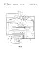
- FIG. 1is a sectional elevation view of the invention showing the integrated circuit oriented at a near normal angle to the laser beam.
- FIG. 2is a further view showing the integrated circuit oriented at an acute angle of incidence to the laser beam.
- a decapsulation apparatus 100that comprises a chamber wall 12 that encloses and seals a chamber 20 .
- the chamber 20has a clean gas inlet 11 with a conduit 22 that directs a stream of clean gas, such as nitrogen or compressed air at a device under test (DUT), i.e., integrated circuit 24 .
- Chamber 20also has an exhaust port 9 for removing fumes and dust particles from the chamber.
- a stage 2that is disposed over a dust bin 3 .
- the dust bin 3catches dust and debris that are generated by the laser striking the plastic resin on the DUT 24 .
- a laser 8is mounted on the outside wall 12 of the chamber 20 .
- the laserdirects a laser beam 26 toward the DUT 24 .
- the laser 8is any suitable laser, such as a YAG or an infrared laser.
- the laser 8has its frequency and its intensity (power) tunable for removing plastic encapsulant from the DUT 24 without causing damage to the encapsulated integrated circuit.
- the laser beam 26passes through an optical opening or window (not shown) in the wall 12 of the chamber 20 .
- the interior of the chamber 20is illuminated by a suitable light 7 . Operation of the laser on the DUT 24 is observed through a microscope 5 . This is also mounted on wall 12 .
- the microscope 5has a shutter 6 that may be manually or automatically operated as hereinafter described.
- Light reflected from the surface of the DUT 24is detected by endpoint detector 10 .
- the endpoint detector 10senses the amplitude or frequency or both of the reflected light.
- the endpoint detectoris any suitable photo
- the stage 2is an X,Y positioning table. It is desirable that the stage be made of rods or a perforated table so that dust and debris removed from the DUT 24 falls through the stage and the stage mount into the dust bin 3 .
- Such X,Y positioning tablesare well known in the art. They maybe operated using piezoelectric operators, linear magnetic motors, or lead screws.
- the DUT 24is disposed at substantially a normal angle to the laser beam 26 .
- the stageis hinged at one end 4 so that the DUT 24 may be rotated to a substantially vertical position as shown in FIG. 2 . In its vertical position, the laser beam 26 has an acute angle of incidence with the surface of the DUT 24 . That particular position is useful when it is desired to leave a thin layer of encapsulant on the surface of the integrated circuit. Leaving such a thin layer is often desired during failure analysis to detect contaminants on the surface of the encapsulated DUT 24 .
- the apparatus 100may be manually operated or automatically operated or may be semiautomatically operated.
- the apparatus 100is provided with a controller 50 .
- the controller 50includes a CPU 51 which may be a microprocessor or a digital signal processor.
- the CPU 51communicates with a random access memory 53 and a read-only memory 54 . Suitable operating software and application software are stored in the RAM 53 or ROM 54 .
- the CPU 51controls operations of the various components of the apparatus 100 via the control bus 30 and the control lines 31 - 37 that are respectively connected to the microscope shutter 6 , laser 8 , stage 2 , clean gas inlet 11 , endpoint detector 10 , exhaust port 9 , and joy stick 40 .
- the operatormay selectively operate any one of the controlled components, move the stage to its desired X,Y position, and rotate the top platform of the stage to its desired Z axis orientation.
- wavelengths in the infrared rangeare especially applicable: 725-900 cm ⁇ 1, 1150-1300 cm ⁇ 1, 1400-1500 cm ⁇ 1 and 1600-1750 cm ⁇ 1.
- These wavelength rangeswere determined from IR chemical analysis of the mold compound resins. See “Identifying Plastic Encapsulant Materials by Pyrolysis Infrared Spectrophotometry”, R. K. Lowry, K. L. Hanley, Proceedings, 1998 Intl Symposium for Testing and Failure Analysis, November, 1998, pp. 399-401. It is these wavelength ranges in particular where there is significant absorption of IR energy at the molecular level by plastic resins. An incident beam tuned for maximized power in these energy ranges begins to promote molecular rearrangement and ultimately decompositional breakdown of polymerized resin molecules.
- Any tuned laser operating in these rangespromotes breakdown not just by thermal heating the material (which almost any incident laser energy with enough power could provide) but also by chemical decomposition. This promotes breakdown in a “material-specific” way, so that excessive heating via straightforward but less-controllable thermal decomposition can be avoided.
- a DUT 24is placed or otherwise mounted on the top of the stage 2 . While the embodiment shown in FIG. 1 includes only a single device, those skilled in the art will appreciate that multiple devices may be mounted on the stage. Either manually or with the assistance of controller 50 , the stage 2 is positioned in an X,Y plane relative to the laser beam 26 . of laser 8 . Laser 8 is under control of the controller 50 . Laser 8 may be any suitable laser that has its amplitude and frequency tuned and controlled by controller 50 . Such suitable lasersinclude YAG lasers, as well as infrared lasers. It is desired to use a laser with a suitable power and frequency for breaking the cross-linked polymeric bonds of the plastic resin that encapsulates the DUT 24 .
- the lasermay be operated at a relatively low level to provide a target beam that strikes the stage and the DUT 24 .
- the operatormay then position the stage by using a joy stick device 40 and the microscope 5 .
- the stageis moved to initially place the laser on one of the corners of the DUT 24 .
- the stagemoves in a raster pattern along a first axis, steps transverse to the first axis at least the width of the beam, and then reverses direction and travels back along the first axis.
- the beam 26raster-scans across the DUT 24 .
- the laser beam 26may be raster-scanned using optical methods, including prisms and/or mirrors that are selectively moved to sweep the beam across the surface of the DUT 24 .
- the plastic encapsulantis removed from the DUT 24 .
- the removal processcreates a cloud of debris and fumes.
- the fumes and some lighter debris particlesare withdrawn from the chamber 20 via the exhaust port 9 .
- the heavier debris particlesfall through the rods or holes in the stage 2 and are captured in the dust bin 3 .
- Some of the dustmay settle onto the DUT 24 .
- Clean gas 22drives the dust away from the DUT 24 .
- the clean gas 22includes any suitable gas, such as nitrogen or air for dispersing the dust particles away from the surface of the DUT 24 . Such dispersal permits the operator to view the DUT in process and removes particles from the immediate path of the laser so that the encapsulant is more effectively removed.
- Decapsulationmay be carried out automatically. During automatic decapsulation, the laser is operated until the endpoint detector 10 detects a change in the amplitude and/or frequency of light reflected from the DUT 24 . When the integrated circuit is uncovered, the reflected light changes its frequency. The intensity of reflected light may also change. The DUT detects these changes and provides a signal via signal and control line 35 to the controller 50 .
- Controller 50receives and sends signals on control and sensor bus 30 via an A-to-D and D-to-A converter 52 .
- the control and sensing signalsare analog signals. Thus, it is necessary to convert the analog signals to digital signals so that they can be understood by the CPU 51 . If the CPU 51 is a DSP, the DSP has a built-in A-to-D and D-to-A converter.
- Controller 50receives the signal from the endpoint detector 10 .
- the controller 50advances the stage to the next position to continue removing encapsulant.
- the laseris focused on the DUT 24 until the underlying integrated circuit is exposed.
- the stageis moved in a continuous or stepwise pattern to subsequent positions.
Landscapes
- Engineering & Computer Science (AREA)
- Physics & Mathematics (AREA)
- Optics & Photonics (AREA)
- Power Engineering (AREA)
- Computer Hardware Design (AREA)
- Microelectronics & Electronic Packaging (AREA)
- Manufacturing & Machinery (AREA)
- Plasma & Fusion (AREA)
- Electromagnetism (AREA)
- General Physics & Mathematics (AREA)
- Condensed Matter Physics & Semiconductors (AREA)
- Mechanical Engineering (AREA)
- Chemical & Material Sciences (AREA)
- Crystallography & Structural Chemistry (AREA)
- Encapsulation Of And Coatings For Semiconductor Or Solid State Devices (AREA)
- Laser Beam Processing (AREA)
- Testing Or Measuring Of Semiconductors Or The Like (AREA)
- Treatments Of Macromolecular Shaped Articles (AREA)
- Processing And Handling Of Plastics And Other Materials For Molding In General (AREA)
Abstract
Description
Claims (2)
Priority Applications (9)
| Application Number | Priority Date | Filing Date | Title |
|---|---|---|---|
| US09/307,896US6335208B1 (en) | 1999-05-10 | 1999-05-10 | Laser decapsulation method |
| TW089103687ATW451364B (en) | 1999-05-10 | 2000-03-02 | Method and apparatus for removing a plastic resin encapsulant from an encapsulated integrated circuit |
| EP00108967AEP1052691A3 (en) | 1999-05-10 | 2000-04-27 | Laser decapsulation apparatus and method |
| KR1020000023224AKR20000077118A (en) | 1999-05-10 | 2000-05-01 | Laser Decapsulation Apparatus And Method |
| JP2000133336AJP2000334586A (en) | 1999-05-10 | 2000-05-02 | Apparatus and method for removing encapsulant by laser |
| US09/949,736US7166186B2 (en) | 1999-05-10 | 2001-09-10 | Laser decapsulation apparatus and method |
| US11/616,617US7316936B2 (en) | 1999-05-10 | 2006-12-27 | Laser decapsulation method |
| US12/435,441USRE42193E1 (en) | 1999-05-10 | 2009-05-05 | Laser decapsulation method |
| US13/032,199USRE43980E1 (en) | 1999-05-10 | 2011-02-22 | Laser decapsulation method |
Applications Claiming Priority (1)
| Application Number | Priority Date | Filing Date | Title |
|---|---|---|---|
| US09/307,896US6335208B1 (en) | 1999-05-10 | 1999-05-10 | Laser decapsulation method |
Related Child Applications (2)
| Application Number | Title | Priority Date | Filing Date |
|---|---|---|---|
| US09/949,736DivisionUS7166186B2 (en) | 1999-05-10 | 2001-09-10 | Laser decapsulation apparatus and method |
| US11/616,617DivisionUS7316936B2 (en) | 1999-05-10 | 2006-12-27 | Laser decapsulation method |
Publications (1)
| Publication Number | Publication Date |
|---|---|
| US6335208B1true US6335208B1 (en) | 2002-01-01 |
Family
ID=23191632
Family Applications (5)
| Application Number | Title | Priority Date | Filing Date |
|---|---|---|---|
| US09/307,896Expired - LifetimeUS6335208B1 (en) | 1999-05-10 | 1999-05-10 | Laser decapsulation method |
| US09/949,736Expired - LifetimeUS7166186B2 (en) | 1999-05-10 | 2001-09-10 | Laser decapsulation apparatus and method |
| US11/616,617CeasedUS7316936B2 (en) | 1999-05-10 | 2006-12-27 | Laser decapsulation method |
| US12/435,441CeasedUSRE42193E1 (en) | 1999-05-10 | 2009-05-05 | Laser decapsulation method |
| US13/032,199Expired - LifetimeUSRE43980E1 (en) | 1999-05-10 | 2011-02-22 | Laser decapsulation method |
Family Applications After (4)
| Application Number | Title | Priority Date | Filing Date |
|---|---|---|---|
| US09/949,736Expired - LifetimeUS7166186B2 (en) | 1999-05-10 | 2001-09-10 | Laser decapsulation apparatus and method |
| US11/616,617CeasedUS7316936B2 (en) | 1999-05-10 | 2006-12-27 | Laser decapsulation method |
| US12/435,441CeasedUSRE42193E1 (en) | 1999-05-10 | 2009-05-05 | Laser decapsulation method |
| US13/032,199Expired - LifetimeUSRE43980E1 (en) | 1999-05-10 | 2011-02-22 | Laser decapsulation method |
Country Status (5)
| Country | Link |
|---|---|
| US (5) | US6335208B1 (en) |
| EP (1) | EP1052691A3 (en) |
| JP (1) | JP2000334586A (en) |
| KR (1) | KR20000077118A (en) |
| TW (1) | TW451364B (en) |
Cited By (20)
| Publication number | Priority date | Publication date | Assignee | Title |
|---|---|---|---|---|
| US20020190396A1 (en)* | 2000-08-16 | 2002-12-19 | Brand Joseph M. | Method and apparatus for removing encapsulating material from a packaged microelectronic device |
| US6500758B1 (en)* | 2000-09-12 | 2002-12-31 | Eco-Snow Systems, Inc. | Method for selective metal film layer removal using carbon dioxide jet spray |
| US20030010761A1 (en)* | 2001-07-11 | 2003-01-16 | Hong Ming Hui | Method and apparatus for decapping integrated circuit packages |
| US6579376B1 (en)* | 1999-08-16 | 2003-06-17 | Canon Kabushiki Kaisha | Method and apparatus for opening resin-sealed body |
| US20030127423A1 (en)* | 2002-01-07 | 2003-07-10 | Dlugokecki Joseph J. | Method for reconstructing an integrated circuit package using lapping |
| US20040130718A1 (en)* | 2003-01-08 | 2004-07-08 | Kla-Tencor Technologies Corporation | Concurrent measurement and cleaning of thin films on silicon-on-insulator (SOI) |
| US6813828B2 (en) | 2002-01-07 | 2004-11-09 | Gel Pak L.L.C. | Method for deconstructing an integrated circuit package using lapping |
| WO2004059284A3 (en)* | 2002-12-20 | 2004-11-25 | Dakocytomation Denmark As | Apparatus for automated processing biological samples |
| US20060099886A1 (en)* | 2004-11-10 | 2006-05-11 | Joseph Rubin | Electronic die positioning device and method |
| US7067332B1 (en)* | 2004-03-16 | 2006-06-27 | Altera Corporation | Method for die removal from plastic packages |
| US20070075050A1 (en)* | 2005-06-30 | 2007-04-05 | Jon Heyl | Semiconductor failure analysis tool |
| US20070111337A1 (en)* | 1999-05-10 | 2007-05-17 | Lowry Robert K | Laser decapsulation apparatus and method |
| US20100258544A1 (en)* | 2007-11-26 | 2010-10-14 | Tsuneo Kurita | Mold removing method |
| US20110007308A1 (en)* | 2009-07-08 | 2011-01-13 | Universidade De Vigo | Method for removal of wax from porous stones in historical monuments |
| US20110115129A1 (en)* | 2008-07-09 | 2011-05-19 | Fei Company | Method and Apparatus for Laser Machining |
| US20110141205A1 (en)* | 2009-12-15 | 2011-06-16 | Xerox Corporation | Method of Removing Thermoset Polymer From Piezoelectric Transducers in a Print Head |
| US20140184782A1 (en)* | 2012-12-28 | 2014-07-03 | Samsung Electro-Mechanics Co., Ltd. | System of measuring warpage and method of measuring warpage |
| RU169247U1 (en)* | 2016-08-23 | 2017-03-13 | Закрытое акционерное общество "ГРУППА КРЕМНИЙ ЭЛ" | DEVICE FOR OPENING PLASTIC CASES OF SEMICONDUCTOR DEVICES AND MICROSHEELS LASER |
| RU199130U1 (en)* | 2020-03-16 | 2020-08-17 | Акционерное общество "ГРУППА КРЕМНИЙ ЭЛ" | MASK FOR DECORPING MICROELECTRONICS DEVICES IN A POLYMER CASE |
| CN119927461A (en)* | 2025-03-26 | 2025-05-06 | 火星智能科技(南通)有限公司 | A CNC machine tool laser cutting device |
Families Citing this family (19)
| Publication number | Priority date | Publication date | Assignee | Title |
|---|---|---|---|---|
| EP1440608B1 (en)* | 2001-11-02 | 2006-02-15 | ATMEL Germany GmbH | Method for opening the plastic housing of an electronic module |
| FR2837733B1 (en)* | 2002-03-28 | 2005-01-14 | Centre Nat Etd Spatiales | METHOD AND DEVICE FOR ABLATION OF A COVER LAYER COVERING A SURFACE TO BE BORN |
| DE10324181A1 (en)* | 2003-05-28 | 2004-12-23 | Messer Griesheim Gmbh | Shielding gas device for laser material processing |
| US7271012B2 (en)* | 2003-07-15 | 2007-09-18 | Control Systemation, Inc. | Failure analysis methods and systems |
| US7553680B2 (en)* | 2004-08-09 | 2009-06-30 | Delphi Technologies, Inc. | Methods to provide and expose a diagnostic connector on overmolded electronic packages |
| GB2434767A (en)* | 2006-02-02 | 2007-08-08 | Xsil Technology Ltd | Laser machining |
| JP5061962B2 (en)* | 2008-03-04 | 2012-10-31 | 住友電気工業株式会社 | Laser processing method and laser processing apparatus |
| JP2009291815A (en)* | 2008-06-05 | 2009-12-17 | Kyushu Mitoyo Kk | Laser beam machining apparatus |
| DE102008045336B4 (en) | 2008-09-01 | 2022-05-25 | Carl Zeiss Microscopy Gmbh | System for processing a sample with a laser beam and an electron beam or an ion beam |
| DE102009011961A1 (en)* | 2009-03-10 | 2010-09-16 | Advanced Nuclear Fuels Gmbh | Suction device for gases or smoke, in particular welding fume, welding system and associated method |
| TW201207913A (en)* | 2010-08-13 | 2012-02-16 | Msscorps Co Ltd | Two-stage encapsulation removing method for semiconductor device and laser grooving device |
| DE102011001322A1 (en)* | 2011-03-16 | 2012-09-20 | Ipg Laser Gmbh | Machine and method for material processing of workpieces with a laser beam |
| US8974731B2 (en) | 2011-08-04 | 2015-03-10 | Analogic Corporation | Sample carrier and/or sample carrier processing apparatus |
| CN102998957B (en)* | 2011-09-09 | 2015-06-24 | 珠海艾派克微电子有限公司 | Imaging box chip restoration method |
| KR101814493B1 (en)* | 2016-05-30 | 2018-01-04 | 주식회사 아이엠티 | apparatus and method of selective removal of molding resin on semiconductor |
| CN108195835A (en)* | 2017-12-13 | 2018-06-22 | 中国北方车辆研究所 | A kind of recognition methods for palming off renovation plastic packaging component |
| CN113013021A (en)* | 2021-03-01 | 2021-06-22 | 长江存储科技有限责任公司 | Unsealing method of semiconductor packaging structure |
| US12106973B2 (en) | 2021-10-28 | 2024-10-01 | Silicon Laboratories Inc. | Two-step decapsulation technique for semiconductor package having silver bond wires |
| CN116013817B (en)* | 2023-01-17 | 2024-03-19 | 上海季丰电子股份有限公司 | Chip packaging breaking device and method |
Citations (11)
| Publication number | Priority date | Publication date | Assignee | Title |
|---|---|---|---|---|
| WO1986007492A1 (en)* | 1985-06-11 | 1986-12-18 | American Telephone & Telegraph Company | Lead frame deflashing |
| GB2177965A (en)* | 1985-07-24 | 1987-02-04 | Philips Electronic Associated | Manufacturing an electrical device |
| US5182230A (en)* | 1988-07-25 | 1993-01-26 | International Business Machines Corporation | Laser methods for circuit repair on integrated circuits and substrates |
| US5281798A (en)* | 1991-12-24 | 1994-01-25 | Maxwell Laboratories, Inc. | Method and system for selective removal of material coating from a substrate using a flashlamp |
| US5424254A (en)* | 1994-02-22 | 1995-06-13 | International Business Machines Corporation | Process for recovering bare semiconductor chips from plastic packaged modules by thermal shock |
| FR2731637A1 (en)* | 1995-03-16 | 1996-09-20 | Aerospatiale | Photo:ablation by laser beam to remove particle-filled polymers |
| US5643472A (en)* | 1988-07-08 | 1997-07-01 | Cauldron Limited Partnership | Selective removal of material by irradiation |
| US5700697A (en)* | 1993-02-01 | 1997-12-23 | Silicon Packaging Technology | Method for packaging an integrated circuit using a reconstructed package |
| US5817243A (en)* | 1996-10-30 | 1998-10-06 | Shaffer; Wayne K. | Method for applying decorative contrast designs to automotive and motorcycle parts using lasers |
| US5824569A (en)* | 1992-07-15 | 1998-10-20 | Micron Technology, Inc. | Semiconductor device having ball-bonded pads |
| US6048588A (en)* | 1988-07-08 | 2000-04-11 | Cauldron Limited Partnership | Method for enhancing chemisorption of material |
Family Cites Families (31)
| Publication number | Priority date | Publication date | Assignee | Title |
|---|---|---|---|---|
| US4052603A (en)* | 1974-12-23 | 1977-10-04 | International Business Machines Corporation | Object positioning process and apparatus |
| JPS6172030A (en)* | 1984-09-18 | 1986-04-14 | Mitsubishi Electric Corp | Method for accelerating resin melting of electronic parts |
| JPS6332957A (en)* | 1986-07-25 | 1988-02-12 | Matsushita Electronics Corp | Manufacture of semiconductor device |
| DE3824273A1 (en)* | 1988-07-16 | 1990-01-18 | Philips Patentverwaltung | METHOD FOR PRODUCING SOLID BODIES |
| DE4000690A1 (en)* | 1990-01-12 | 1991-07-18 | Philips Patentverwaltung | PROCESS FOR PRODUCING ULTRAFINE PARTICLES AND THEIR USE |
| DE4138157A1 (en)* | 1991-11-21 | 1993-05-27 | Krupp Ag | Measuring thickness of coating, e.g. of zinc@ on steel, - counting repeatedly applied laser pulses until spectral lines in plasma generated changes |
| JP2707189B2 (en)* | 1992-08-26 | 1998-01-28 | 株式会社日立製作所 | Method and apparatus for removing electronic component from substrate |
| DE4229399C2 (en)* | 1992-09-03 | 1999-05-27 | Deutsch Zentr Luft & Raumfahrt | Method and device for producing a functional structure of a semiconductor component |
| JPH0870144A (en) | 1994-08-26 | 1996-03-12 | Sumitomo Electric Ind Ltd | How to make superconducting parts |
| US5961860A (en)* | 1995-06-01 | 1999-10-05 | National University Of Singapore | Pulse laser induced removal of mold flash on integrated circuit packages |
| US5937270A (en) | 1996-01-24 | 1999-08-10 | Micron Electronics, Inc. | Method of efficiently laser marking singulated semiconductor devices |
| US6043100A (en)* | 1996-04-19 | 2000-03-28 | Weaver; Kevin | Chip on tape die reframe process |
| US5986234A (en) | 1997-03-28 | 1999-11-16 | The Regents Of The University Of California | High removal rate laser-based coating removal system |
| US6392683B1 (en) | 1997-09-26 | 2002-05-21 | Sumitomo Heavy Industries, Ltd. | Method for making marks in a transparent material by using a laser |
| JP3511359B2 (en) | 1998-02-27 | 2004-03-29 | 三菱電機株式会社 | Laser processing equipment |
| US6140604A (en)* | 1998-06-18 | 2000-10-31 | General Electric Company | Laser drilling breakthrough detector |
| EP1116165A2 (en) | 1998-08-31 | 2001-07-18 | Siemens Aktiengesellschaft | Method for producing metallic microstructures and use of this method in the production of sensor devices for detecting fingerprints |
| US6710284B1 (en) | 1999-02-26 | 2004-03-23 | Micron Technology, Inc. | Laser marking techniques for bare semiconductor die |
| US6414320B1 (en) | 1999-05-03 | 2002-07-02 | The Regents Of The University Of California | Composition analysis by scanning femtosecond laser ultraprobing (CASFLU). |
| US6335208B1 (en)* | 1999-05-10 | 2002-01-01 | Intersil Americas Inc. | Laser decapsulation method |
| US6329272B1 (en)* | 1999-06-14 | 2001-12-11 | Technologies Ltrim Inc. | Method and apparatus for iteratively, selectively tuning the impedance of integrated semiconductor devices using a focussed heating source |
| FR2797956B1 (en) | 1999-08-26 | 2001-11-30 | Univ Metz | LASER ABLATION DETECTION AND ANALYSIS DEVICE AND TRANSFER TO AN ION TRAP OF A SPECTROMETER, METHOD USING THE SAME AND PARTICULAR USES OF THE METHOD |
| AU7101000A (en) | 1999-09-10 | 2001-04-10 | Caliper Technologies Corporation | Microfabrication methods and devices |
| US6887804B2 (en) | 2000-01-10 | 2005-05-03 | Electro Scientific Industries, Inc. | Passivation processing over a memory link |
| SG111023A1 (en) | 2001-07-11 | 2005-05-30 | Inst Data Storage | Method and apparatus for decapping integrated circuit packages |
| US6875950B2 (en) | 2002-03-22 | 2005-04-05 | Gsi Lumonics Corporation | Automated laser trimming of resistors |
| US7271012B2 (en) | 2003-07-15 | 2007-09-18 | Control Systemation, Inc. | Failure analysis methods and systems |
| US9022037B2 (en) | 2003-08-11 | 2015-05-05 | Raydiance, Inc. | Laser ablation method and apparatus having a feedback loop and control unit |
| US7528342B2 (en) | 2005-02-03 | 2009-05-05 | Laserfacturing, Inc. | Method and apparatus for via drilling and selective material removal using an ultrafast pulse laser |
| US20070012665A1 (en) | 2005-07-12 | 2007-01-18 | Hewlett-Packard Development Company Lp | Laser ablation |
| CA2624200A1 (en) | 2005-10-03 | 2007-04-12 | Aradigm Corporation | Method and system for laser machining |
- 1999
- 1999-05-10USUS09/307,896patent/US6335208B1/ennot_activeExpired - Lifetime
- 2000
- 2000-03-02TWTW089103687Apatent/TW451364B/ennot_activeIP Right Cessation
- 2000-04-27EPEP00108967Apatent/EP1052691A3/ennot_activeWithdrawn
- 2000-05-01KRKR1020000023224Apatent/KR20000077118A/ennot_activeWithdrawn
- 2000-05-02JPJP2000133336Apatent/JP2000334586A/enactivePending
- 2001
- 2001-09-10USUS09/949,736patent/US7166186B2/ennot_activeExpired - Lifetime
- 2006
- 2006-12-27USUS11/616,617patent/US7316936B2/ennot_activeCeased
- 2009
- 2009-05-05USUS12/435,441patent/USRE42193E1/ennot_activeCeased
- 2011
- 2011-02-22USUS13/032,199patent/USRE43980E1/ennot_activeExpired - Lifetime
Patent Citations (11)
| Publication number | Priority date | Publication date | Assignee | Title |
|---|---|---|---|---|
| WO1986007492A1 (en)* | 1985-06-11 | 1986-12-18 | American Telephone & Telegraph Company | Lead frame deflashing |
| GB2177965A (en)* | 1985-07-24 | 1987-02-04 | Philips Electronic Associated | Manufacturing an electrical device |
| US5643472A (en)* | 1988-07-08 | 1997-07-01 | Cauldron Limited Partnership | Selective removal of material by irradiation |
| US6048588A (en)* | 1988-07-08 | 2000-04-11 | Cauldron Limited Partnership | Method for enhancing chemisorption of material |
| US5182230A (en)* | 1988-07-25 | 1993-01-26 | International Business Machines Corporation | Laser methods for circuit repair on integrated circuits and substrates |
| US5281798A (en)* | 1991-12-24 | 1994-01-25 | Maxwell Laboratories, Inc. | Method and system for selective removal of material coating from a substrate using a flashlamp |
| US5824569A (en)* | 1992-07-15 | 1998-10-20 | Micron Technology, Inc. | Semiconductor device having ball-bonded pads |
| US5700697A (en)* | 1993-02-01 | 1997-12-23 | Silicon Packaging Technology | Method for packaging an integrated circuit using a reconstructed package |
| US5424254A (en)* | 1994-02-22 | 1995-06-13 | International Business Machines Corporation | Process for recovering bare semiconductor chips from plastic packaged modules by thermal shock |
| FR2731637A1 (en)* | 1995-03-16 | 1996-09-20 | Aerospatiale | Photo:ablation by laser beam to remove particle-filled polymers |
| US5817243A (en)* | 1996-10-30 | 1998-10-06 | Shaffer; Wayne K. | Method for applying decorative contrast designs to automotive and motorcycle parts using lasers |
Cited By (68)
| Publication number | Priority date | Publication date | Assignee | Title |
|---|---|---|---|---|
| USRE43980E1 (en) | 1999-05-10 | 2013-02-05 | Intersil Corporation | Laser decapsulation method |
| US20070111337A1 (en)* | 1999-05-10 | 2007-05-17 | Lowry Robert K | Laser decapsulation apparatus and method |
| US7316936B2 (en) | 1999-05-10 | 2008-01-08 | Intersil Americans Inc. | Laser decapsulation method |
| USRE42193E1 (en) | 1999-05-10 | 2011-03-01 | Intersil Corporation | Laser decapsulation method |
| US6579376B1 (en)* | 1999-08-16 | 2003-06-17 | Canon Kabushiki Kaisha | Method and apparatus for opening resin-sealed body |
| US7405487B2 (en) | 2000-08-16 | 2008-07-29 | Micron Technology, Inc. | Method and apparatus for removing encapsulating material from a packaged microelectronic device |
| US20020190396A1 (en)* | 2000-08-16 | 2002-12-19 | Brand Joseph M. | Method and apparatus for removing encapsulating material from a packaged microelectronic device |
| US20070031998A1 (en)* | 2000-08-16 | 2007-02-08 | Micron Technology, Inc. | Method and apparatus for removing encapsulating material from a packaged microelectronic device |
| US7273769B1 (en)* | 2000-08-16 | 2007-09-25 | Micron Technology, Inc. | Method and apparatus for removing encapsulating material from a packaged microelectronic device |
| US6500758B1 (en)* | 2000-09-12 | 2002-12-31 | Eco-Snow Systems, Inc. | Method for selective metal film layer removal using carbon dioxide jet spray |
| US6917011B2 (en)* | 2001-07-11 | 2005-07-12 | Advanced Micro Devices Pte Ltd. | Method and apparatus for decapping integrated circuit packages |
| US20030010761A1 (en)* | 2001-07-11 | 2003-01-16 | Hong Ming Hui | Method and apparatus for decapping integrated circuit packages |
| US6813828B2 (en) | 2002-01-07 | 2004-11-09 | Gel Pak L.L.C. | Method for deconstructing an integrated circuit package using lapping |
| US20030127423A1 (en)* | 2002-01-07 | 2003-07-10 | Dlugokecki Joseph J. | Method for reconstructing an integrated circuit package using lapping |
| US6884663B2 (en) | 2002-01-07 | 2005-04-26 | Delphon Industries, Llc | Method for reconstructing an integrated circuit package using lapping |
| US8663978B2 (en) | 2002-12-20 | 2014-03-04 | Dako Denmark A/S | Method and apparatus for automatic staining of tissue samples |
| US8257968B2 (en) | 2002-12-20 | 2012-09-04 | Dako Denmark A/S | Method and apparatus for automatic staining of tissue samples |
| US20060088940A1 (en)* | 2002-12-20 | 2006-04-27 | Dakocytomation Denmark A/S | Isolated communication sample processing system and methods of biological slide processing |
| US10156580B2 (en) | 2002-12-20 | 2018-12-18 | Dako Denmark A/S | Information notification sample processing system and methods of biological slide processing |
| US9778273B2 (en) | 2002-12-20 | 2017-10-03 | Dako Denmark A/S | Isolated communication sample processing system and methods of biological slide processing |
| US9599630B2 (en) | 2002-12-20 | 2017-03-21 | Dako Denmark A/S | Method and apparatus for automatic staining of tissue samples |
| US20060172426A1 (en)* | 2002-12-20 | 2006-08-03 | Dakocytomation Denmark A/S | Systems and methods of sample processing and temperature control |
| US20060063265A1 (en)* | 2002-12-20 | 2006-03-23 | Dakocytomation Denmark A/S | Advance programmed sample processing system and methods of biological slide processing |
| US9229016B2 (en) | 2002-12-20 | 2016-01-05 | Dako Denmark A/S | Information notification sample processing system and methods of biological slide processing |
| US20060045806A1 (en)* | 2002-12-20 | 2006-03-02 | Dakocytomation Denmark A/S | Apparatus for automated processing biological samples |
| US20060046298A1 (en)* | 2002-12-20 | 2006-03-02 | Dako-Cytomation Denmark A/S | Enhanced scheduling sample processing system and methods of biological slide processing |
| US8969086B2 (en) | 2002-12-20 | 2015-03-03 | Dako Denmark A/S | Enhanced scheduling sample processing system and methods of biological slide processing |
| US7400983B2 (en) | 2002-12-20 | 2008-07-15 | Dako Denmark A/S | Information notification sample processing system and methods of biological slide processing |
| US20050064535A1 (en)* | 2002-12-20 | 2005-03-24 | Dako Cytomation Denmark A/S | Method and apparatus for pretreatment of tissue slides |
| US20080241876A1 (en)* | 2002-12-20 | 2008-10-02 | Dako Denmark A/S | Information notification sample processing system and methods of biological slide processing |
| US7648678B2 (en) | 2002-12-20 | 2010-01-19 | Dako Denmark A/S | Method and system for pretreatment of tissue slides |
| US8788217B2 (en) | 2002-12-20 | 2014-07-22 | Dako Denmark A/S | Information notification sample processing system and methods of biological slide processing |
| US7758809B2 (en) | 2002-12-20 | 2010-07-20 | Dako Cytomation Denmark A/S | Method and system for pretreatment of tissue slides |
| US8784735B2 (en) | 2002-12-20 | 2014-07-22 | Dako Denmark A/S | Apparatus for automated processing biological samples |
| US8673642B2 (en) | 2002-12-20 | 2014-03-18 | Dako Denmark A/S | Enhanced scheduling sample processing system and methods of biological slide processing |
| US20040266015A1 (en)* | 2002-12-20 | 2004-12-30 | Dakocytomation Denmark A/S | Automated sample processing apparatus and a method of automated treating of samples and use of such apparatus |
| US7937228B2 (en) | 2002-12-20 | 2011-05-03 | Dako Denmark A/S | Information notification sample processing system and methods of biological slide processing |
| US8529836B2 (en) | 2002-12-20 | 2013-09-10 | Dako Denmark A/S | Apparatus for automated processing biological samples |
| US7960178B2 (en) | 2002-12-20 | 2011-06-14 | Dako Denmark A/S | Enhanced scheduling sample processing system and methods of biological slide processing |
| US8394635B2 (en) | 2002-12-20 | 2013-03-12 | Dako Denmark A/S | Enhanced scheduling sample processing system and methods of biological slide processing |
| US20110167930A1 (en)* | 2002-12-20 | 2011-07-14 | Gordon Feingold | Information notification sample processing system and methods of biological slide processing |
| US8386195B2 (en) | 2002-12-20 | 2013-02-26 | Dako Denmark A/S | Information notification sample processing system and methods of biological slide processing |
| US8216512B2 (en) | 2002-12-20 | 2012-07-10 | Dako Denmark A/S | Apparatus for automated processing biological samples |
| US20060088928A1 (en)* | 2002-12-20 | 2006-04-27 | Dakocytomation Denmark A/S | Method and apparatus for automatic staining of tissue samples |
| US8298815B2 (en) | 2002-12-20 | 2012-10-30 | Dako Denmark A/S | Systems and methods of sample processing and temperature control |
| WO2004059284A3 (en)* | 2002-12-20 | 2004-11-25 | Dakocytomation Denmark As | Apparatus for automated processing biological samples |
| US20040130718A1 (en)* | 2003-01-08 | 2004-07-08 | Kla-Tencor Technologies Corporation | Concurrent measurement and cleaning of thin films on silicon-on-insulator (SOI) |
| US7006222B2 (en)* | 2003-01-08 | 2006-02-28 | Kla-Tencor Technologies Corporation | Concurrent measurement and cleaning of thin films on silicon-on-insulator (SOI) |
| US7067332B1 (en)* | 2004-03-16 | 2006-06-27 | Altera Corporation | Method for die removal from plastic packages |
| US20060099886A1 (en)* | 2004-11-10 | 2006-05-11 | Joseph Rubin | Electronic die positioning device and method |
| US7066788B2 (en) | 2004-11-10 | 2006-06-27 | Ultra Tec Manufacturing, Inc. | Electronic die positioning device and method |
| US20070075050A1 (en)* | 2005-06-30 | 2007-04-05 | Jon Heyl | Semiconductor failure analysis tool |
| US7705267B2 (en)* | 2005-06-30 | 2010-04-27 | Jon Heyl | Semiconductor failure analysis tool |
| US20100258544A1 (en)* | 2007-11-26 | 2010-10-14 | Tsuneo Kurita | Mold removing method |
| US8309882B2 (en)* | 2007-11-26 | 2012-11-13 | National Institute Of Advanced Industrial Science And Technology | Mold removing method |
| US20110115129A1 (en)* | 2008-07-09 | 2011-05-19 | Fei Company | Method and Apparatus for Laser Machining |
| US8853592B2 (en) | 2008-07-09 | 2014-10-07 | Fei Company | Method for laser machining a sample having a crystalline structure |
| CN102149510B (en)* | 2008-07-09 | 2015-03-11 | Fei公司 | Method and apparatus for laser machining |
| US10493559B2 (en) | 2008-07-09 | 2019-12-03 | Fei Company | Method and apparatus for laser machining |
| US20110007308A1 (en)* | 2009-07-08 | 2011-01-13 | Universidade De Vigo | Method for removal of wax from porous stones in historical monuments |
| US8310670B2 (en)* | 2009-07-08 | 2012-11-13 | Universidade De Vigo | Method for removal of wax from porous stones in historical monuments |
| US8408683B2 (en) | 2009-12-15 | 2013-04-02 | Xerox Corporation | Method of removing thermoset polymer from piezoelectric transducers in a print head |
| US20110141205A1 (en)* | 2009-12-15 | 2011-06-16 | Xerox Corporation | Method of Removing Thermoset Polymer From Piezoelectric Transducers in a Print Head |
| US8197037B2 (en) | 2009-12-15 | 2012-06-12 | Xerox Corporation | Method of removing thermoset polymer from piezoelectric transducers in a print head |
| US20140184782A1 (en)* | 2012-12-28 | 2014-07-03 | Samsung Electro-Mechanics Co., Ltd. | System of measuring warpage and method of measuring warpage |
| RU169247U1 (en)* | 2016-08-23 | 2017-03-13 | Закрытое акционерное общество "ГРУППА КРЕМНИЙ ЭЛ" | DEVICE FOR OPENING PLASTIC CASES OF SEMICONDUCTOR DEVICES AND MICROSHEELS LASER |
| RU199130U1 (en)* | 2020-03-16 | 2020-08-17 | Акционерное общество "ГРУППА КРЕМНИЙ ЭЛ" | MASK FOR DECORPING MICROELECTRONICS DEVICES IN A POLYMER CASE |
| CN119927461A (en)* | 2025-03-26 | 2025-05-06 | 火星智能科技(南通)有限公司 | A CNC machine tool laser cutting device |
Also Published As
| Publication number | Publication date |
|---|---|
| KR20000077118A (en) | 2000-12-26 |
| USRE43980E1 (en) | 2013-02-05 |
| TW451364B (en) | 2001-08-21 |
| US7316936B2 (en) | 2008-01-08 |
| EP1052691A3 (en) | 2003-11-05 |
| EP1052691A2 (en) | 2000-11-15 |
| US20020025600A1 (en) | 2002-02-28 |
| US7166186B2 (en) | 2007-01-23 |
| JP2000334586A (en) | 2000-12-05 |
| USRE42193E1 (en) | 2011-03-01 |
| US20070111337A1 (en) | 2007-05-17 |
Similar Documents
| Publication | Publication Date | Title |
|---|---|---|
| US6335208B1 (en) | Laser decapsulation method | |
| US6917011B2 (en) | Method and apparatus for decapping integrated circuit packages | |
| EP0247331B1 (en) | Removal of excess material from a semiconductor wafer | |
| US6949147B2 (en) | In situ module for particle removal from solid-state surfaces | |
| JP2013070097A (en) | Method of processing transportation support for transporting and storing semiconductor substrate in atmosphere, and processing station for carrying out such method | |
| KR20010099947A (en) | Local vectorial particle cleaning | |
| US5961860A (en) | Pulse laser induced removal of mold flash on integrated circuit packages | |
| JP7387227B2 (en) | Wafer processing method | |
| US20220373321A1 (en) | Protective film thickness measuring method | |
| WO2024250765A1 (en) | Three-dimensional laser ablation mass spectrometer, combined detection system, and detection method | |
| TWI477374B (en) | Device and method for separating electronic components | |
| CN1265933C (en) | Laser processing apparatus | |
| KR20060038146A (en) | Dry cleaning method and cleaning device for image sensor using laser | |
| JP4413831B2 (en) | Wafer surface inspection apparatus and wafer surface inspection method | |
| KR19990074698A (en) | Mold cleaning device | |
| KR20230109551A (en) | Grinding apparatus | |
| KR100708230B1 (en) | Mobile Dry Cleaner | |
| JPH1174238A (en) | Brush cleaning device and brush cleaning method | |
| EP1335801B1 (en) | Apparatus and method for removing particles from solid-state surfaces | |
| JPS61279131A (en) | Semiconductor wafer defect removal equipment | |
| KR20050073711A (en) | Cleaning device of semiconductor package | |
| KR200317833Y1 (en) | System for removing molding resin of electronic part using laser | |
| KR200198459Y1 (en) | Particle removing apparatus of semiconductor wafer | |
| JPH10300684A (en) | Device and method for sampling impurity on substrate surface | |
| JPH1010017A (en) | Particle sampler |
Legal Events
| Date | Code | Title | Description |
|---|---|---|---|
| AS | Assignment | Owner name:HARRIS CORPORATION, FLORIDA Free format text:ASSIGNMENT OF ASSIGNORS INTEREST;ASSIGNOR:LOWRY, ROBERT K.;REEL/FRAME:009949/0421 Effective date:19990506 | |
| AS | Assignment | Owner name:INTERSIL CORPORATION, FLORIDA Free format text:AMEND TO ADD PROPERTIES RECORDED ON REEL 10247, FRAME 0043.;ASSIGNOR:HARRIS CORPORATION;REEL/FRAME:010884/0394 Effective date:19990813 | |
| AS | Assignment | Owner name:CREDIT SUISSE FIRST BOSTON, AS COLLATERAL AGENT, N Free format text:SECURITY INTEREST;ASSIGNOR:INTERSIL CORPORATION;REEL/FRAME:010351/0410 Effective date:19990813 | |
| STCF | Information on status: patent grant | Free format text:PATENTED CASE | |
| FPAY | Fee payment | Year of fee payment:4 | |
| FPAY | Fee payment | Year of fee payment:8 | |
| FPAY | Fee payment | Year of fee payment:12 | |
| AS | Assignment | Owner name:INTERSIL AMERICAS INC., CALIFORNIA Free format text:ASSIGNMENT OF ASSIGNORS INTEREST;ASSIGNOR:INTERSIL COMMUNICATIONS, INC.;REEL/FRAME:033262/0582 Effective date:20011221 Owner name:INTERSIL AMERICAS LLC, CALIFORNIA Free format text:CHANGE OF NAME;ASSIGNOR:INTERSIL AMERICAS INC.;REEL/FRAME:033262/0819 Effective date:20111223 Owner name:INTERSIL COMMUNICATIONS, INC., CALIFORNIA Free format text:CHANGE OF NAME;ASSIGNOR:INTERSIL CORPORATION;REEL/FRAME:033261/0088 Effective date:20010523 |