US6333750B1 - Multi-sourced video distribution hub - Google Patents
Multi-sourced video distribution hubDownload PDFInfo
- Publication number
- US6333750B1 US6333750B1US09/100,582US10058298AUS6333750B1US 6333750 B1US6333750 B1US 6333750B1US 10058298 AUS10058298 AUS 10058298AUS 6333750 B1US6333750 B1US 6333750B1
- Authority
- US
- United States
- Prior art keywords
- video
- data
- signal
- hub
- plural
- Prior art date
- Legal status (The legal status is an assumption and is not a legal conclusion. Google has not performed a legal analysis and makes no representation as to the accuracy of the status listed.)
- Expired - Fee Related
Links
Images


Classifications
- G—PHYSICS
- G06—COMPUTING OR CALCULATING; COUNTING
- G06F—ELECTRIC DIGITAL DATA PROCESSING
- G06F13/00—Interconnection of, or transfer of information or other signals between, memories, input/output devices or central processing units
- G06F13/10—Program control for peripheral devices
- G—PHYSICS
- G09—EDUCATION; CRYPTOGRAPHY; DISPLAY; ADVERTISING; SEALS
- G09G—ARRANGEMENTS OR CIRCUITS FOR CONTROL OF INDICATING DEVICES USING STATIC MEANS TO PRESENT VARIABLE INFORMATION
- G09G5/00—Control arrangements or circuits for visual indicators common to cathode-ray tube indicators and other visual indicators
- G09G5/36—Control arrangements or circuits for visual indicators common to cathode-ray tube indicators and other visual indicators characterised by the display of a graphic pattern, e.g. using an all-points-addressable [APA] memory
- G09G5/39—Control of the bit-mapped memory
- G09G5/395—Arrangements specially adapted for transferring the contents of the bit-mapped memory to the screen
- G09G5/397—Arrangements specially adapted for transferring the contents of two or more bit-mapped memories to the screen simultaneously, e.g. for mixing or overlay
- G—PHYSICS
- G06—COMPUTING OR CALCULATING; COUNTING
- G06F—ELECTRIC DIGITAL DATA PROCESSING
- G06F3/00—Input arrangements for transferring data to be processed into a form capable of being handled by the computer; Output arrangements for transferring data from processing unit to output unit, e.g. interface arrangements
- G06F3/14—Digital output to display device ; Cooperation and interconnection of the display device with other functional units
- G06F3/1423—Digital output to display device ; Cooperation and interconnection of the display device with other functional units controlling a plurality of local displays, e.g. CRT and flat panel display
- G06F3/1431—Digital output to display device ; Cooperation and interconnection of the display device with other functional units controlling a plurality of local displays, e.g. CRT and flat panel display using a single graphics controller
- G—PHYSICS
- G06—COMPUTING OR CALCULATING; COUNTING
- G06F—ELECTRIC DIGITAL DATA PROCESSING
- G06F3/00—Input arrangements for transferring data to be processed into a form capable of being handled by the computer; Output arrangements for transferring data from processing unit to output unit, e.g. interface arrangements
- G06F3/14—Digital output to display device ; Cooperation and interconnection of the display device with other functional units
- G06F3/1423—Digital output to display device ; Cooperation and interconnection of the display device with other functional units controlling a plurality of local displays, e.g. CRT and flat panel display
- G06F3/1446—Digital output to display device ; Cooperation and interconnection of the display device with other functional units controlling a plurality of local displays, e.g. CRT and flat panel display display composed of modules, e.g. video walls
- G—PHYSICS
- G09—EDUCATION; CRYPTOGRAPHY; DISPLAY; ADVERTISING; SEALS
- G09G—ARRANGEMENTS OR CIRCUITS FOR CONTROL OF INDICATING DEVICES USING STATIC MEANS TO PRESENT VARIABLE INFORMATION
- G09G5/00—Control arrangements or circuits for visual indicators common to cathode-ray tube indicators and other visual indicators
- G09G5/003—Details of a display terminal, the details relating to the control arrangement of the display terminal and to the interfaces thereto
- G09G5/006—Details of the interface to the display terminal
- G—PHYSICS
- G09—EDUCATION; CRYPTOGRAPHY; DISPLAY; ADVERTISING; SEALS
- G09G—ARRANGEMENTS OR CIRCUITS FOR CONTROL OF INDICATING DEVICES USING STATIC MEANS TO PRESENT VARIABLE INFORMATION
- G09G5/00—Control arrangements or circuits for visual indicators common to cathode-ray tube indicators and other visual indicators
- G09G5/36—Control arrangements or circuits for visual indicators common to cathode-ray tube indicators and other visual indicators characterised by the display of a graphic pattern, e.g. using an all-points-addressable [APA] memory
- G09G5/363—Graphics controllers
- G—PHYSICS
- G09—EDUCATION; CRYPTOGRAPHY; DISPLAY; ADVERTISING; SEALS
- G09G—ARRANGEMENTS OR CIRCUITS FOR CONTROL OF INDICATING DEVICES USING STATIC MEANS TO PRESENT VARIABLE INFORMATION
- G09G5/00—Control arrangements or circuits for visual indicators common to cathode-ray tube indicators and other visual indicators
- G09G5/36—Control arrangements or circuits for visual indicators common to cathode-ray tube indicators and other visual indicators characterised by the display of a graphic pattern, e.g. using an all-points-addressable [APA] memory
- G09G5/39—Control of the bit-mapped memory
- G09G5/393—Arrangements for updating the contents of the bit-mapped memory
- G—PHYSICS
- G09—EDUCATION; CRYPTOGRAPHY; DISPLAY; ADVERTISING; SEALS
- G09G—ARRANGEMENTS OR CIRCUITS FOR CONTROL OF INDICATING DEVICES USING STATIC MEANS TO PRESENT VARIABLE INFORMATION
- G09G2300/00—Aspects of the constitution of display devices
- G09G2300/02—Composition of display devices
- G09G2300/026—Video wall, i.e. juxtaposition of a plurality of screens to create a display screen of bigger dimensions
- G—PHYSICS
- G09—EDUCATION; CRYPTOGRAPHY; DISPLAY; ADVERTISING; SEALS
- G09G—ARRANGEMENTS OR CIRCUITS FOR CONTROL OF INDICATING DEVICES USING STATIC MEANS TO PRESENT VARIABLE INFORMATION
- G09G2330/00—Aspects of power supply; Aspects of display protection and defect management
- G09G2330/02—Details of power systems and of start or stop of display operation
- G—PHYSICS
- G09—EDUCATION; CRYPTOGRAPHY; DISPLAY; ADVERTISING; SEALS
- G09G—ARRANGEMENTS OR CIRCUITS FOR CONTROL OF INDICATING DEVICES USING STATIC MEANS TO PRESENT VARIABLE INFORMATION
- G09G2340/00—Aspects of display data processing
- G09G2340/04—Changes in size, position or resolution of an image
- G09G2340/0407—Resolution change, inclusive of the use of different resolutions for different screen areas
- G—PHYSICS
- G09—EDUCATION; CRYPTOGRAPHY; DISPLAY; ADVERTISING; SEALS
- G09G—ARRANGEMENTS OR CIRCUITS FOR CONTROL OF INDICATING DEVICES USING STATIC MEANS TO PRESENT VARIABLE INFORMATION
- G09G2340/00—Aspects of display data processing
- G09G2340/12—Overlay of images, i.e. displayed pixel being the result of switching between the corresponding input pixels
- G—PHYSICS
- G09—EDUCATION; CRYPTOGRAPHY; DISPLAY; ADVERTISING; SEALS
- G09G—ARRANGEMENTS OR CIRCUITS FOR CONTROL OF INDICATING DEVICES USING STATIC MEANS TO PRESENT VARIABLE INFORMATION
- G09G2360/00—Aspects of the architecture of display systems
- G09G2360/02—Graphics controller able to handle multiple formats, e.g. input or output formats
- G—PHYSICS
- G09—EDUCATION; CRYPTOGRAPHY; DISPLAY; ADVERTISING; SEALS
- G09G—ARRANGEMENTS OR CIRCUITS FOR CONTROL OF INDICATING DEVICES USING STATIC MEANS TO PRESENT VARIABLE INFORMATION
- G09G2360/00—Aspects of the architecture of display systems
- G09G2360/12—Frame memory handling
- G09G2360/122—Tiling
- G—PHYSICS
- G09—EDUCATION; CRYPTOGRAPHY; DISPLAY; ADVERTISING; SEALS
- G09G—ARRANGEMENTS OR CIRCUITS FOR CONTROL OF INDICATING DEVICES USING STATIC MEANS TO PRESENT VARIABLE INFORMATION
- G09G2360/00—Aspects of the architecture of display systems
- G09G2360/12—Frame memory handling
- G09G2360/128—Frame memory using a Synchronous Dynamic RAM [SDRAM]
- G—PHYSICS
- G09—EDUCATION; CRYPTOGRAPHY; DISPLAY; ADVERTISING; SEALS
- G09G—ARRANGEMENTS OR CIRCUITS FOR CONTROL OF INDICATING DEVICES USING STATIC MEANS TO PRESENT VARIABLE INFORMATION
- G09G2370/00—Aspects of data communication
- G09G2370/04—Exchange of auxiliary data, i.e. other than image data, between monitor and graphics controller
- G09G2370/045—Exchange of auxiliary data, i.e. other than image data, between monitor and graphics controller using multiple communication channels, e.g. parallel and serial
- G09G2370/047—Exchange of auxiliary data, i.e. other than image data, between monitor and graphics controller using multiple communication channels, e.g. parallel and serial using display data channel standard [DDC] communication
- G—PHYSICS
- G09—EDUCATION; CRYPTOGRAPHY; DISPLAY; ADVERTISING; SEALS
- G09G—ARRANGEMENTS OR CIRCUITS FOR CONTROL OF INDICATING DEVICES USING STATIC MEANS TO PRESENT VARIABLE INFORMATION
- G09G5/00—Control arrangements or circuits for visual indicators common to cathode-ray tube indicators and other visual indicators
- G09G5/003—Details of a display terminal, the details relating to the control arrangement of the display terminal and to the interfaces thereto
- G09G5/006—Details of the interface to the display terminal
- G09G5/008—Clock recovery
- H—ELECTRICITY
- H04—ELECTRIC COMMUNICATION TECHNIQUE
- H04N—PICTORIAL COMMUNICATION, e.g. TELEVISION
- H04N9/00—Details of colour television systems
- H04N9/12—Picture reproducers
- H—ELECTRICITY
- H04—ELECTRIC COMMUNICATION TECHNIQUE
- H04N—PICTORIAL COMMUNICATION, e.g. TELEVISION
- H04N9/00—Details of colour television systems
- H04N9/12—Picture reproducers
- H04N9/30—Picture reproducers using solid-state colour display devices
Definitions
- CRTThe historical technology of choice for displaying the data on trading floors has been the CRT. As information needs have grown, so has the size of the CRT necessary to display that data. At the present time, CRT displays with a twenty-one inch diagonal (nineteen inches usable diagonal) is the largest display commonly used, while the seventeen inch CRT (fifteen inches usable diagonal) is the most prevalent display. Multiple monitors are frequently connected to a single host computer to allow large amounts of data be displayed, while requiring only one set of user interaction devices (such as keyboard and mouse) and a single computer.
- user interaction devicessuch as keyboard and mouse
- LCDsLiquid Crystal Displays
- these monitorstypically consume 70% less power, have smaller bezels, and are only three to six inches in depth. Because of their relatively small size, these displays allow trading desks to be made much smaller, and they can be mounted in ways which are difficult and costly with CRTs. Unfortunately, LCD monitors are still quite expensive.
- multi-head displaysare quite common in the desktop trading market.
- multiple graphics cardsare inserted into the host PC, each driving one monitor.
- specialized multi-head graphics cardsare available which can drive two or four heads simultaneously. Both of these methods have substantial drawbacks.
- the firstsuffers in that the limited number of computer bus slots (usually only three PCI-style) available in a typical PC are squandered by the graphics cards.
- the limited number of bus slotsmeans that only three heads may be connected to a single PC using this method.
- the second methodsuffers because the specialized multi-head graphics cards are quite expensive, and tend to lack features present in leading-edge single-head cards.
- One such multi-head cardactually provides on a single card the circuitry normally found on two graphics card in order to drive two displays.
- the present inventionenables the provision of a multi-head virtual monitor from the perspective of a host computer via the use of one or more video distribution hubs.
- Each hubreceives a video signal from a standard graphics card in a PC and generates output signals appropriate for driving a plurality of video displays such as flat panel or Cathode Ray Tube (CRT) video displays.
- the video displaysmay be oriented either horizontally, in landscape mode, or vertically, in portrait mode, or in a combination of landscape and portrait arrangements.
- a single hubcan drive displays of differing resolutions as well as head orientations.
- the hubin combination with host software, can be automatically reconfigured when a display is swapped out to accommodate the newly substituted display.
- the hubis particularly adapted for driving a plurality of flat panel displays such as active matrix flat panel displays, dual scan passive flat panel displays, or a combination of such displays.
- a video graphics system in accordance with the present inventionincludes a video graphics adapter having a host interface for coupling the video graphics adapter to a host computer such as a personal computer, workstation, microcomputer, minicomputer, mainframe or the like, and an output for driving a video data signal, such as an RGB analog video signal.
- the video graphics adapterincludes an “oversize” display buffer which has a buffer capacity greater than that necessary to drive a single video display.
- the video graphics systemfurther includes a video distribution hub which has a video input interface for receiving a video signal, such as the RGB analog video signal from the video graphics adapter, and a plurality of output ports for driving associated displays.
- the video distribution hubreceives the video signal from the video graphics adapter at the video input interface of the video distribution hub and, in the case where the received signal is an analog signal, applies the signal to an analog to digital converter (ADC) to generate digital signals corresponding to red, green and blue data signals.
- ADCanalog to digital converter
- the digital videois applied to a bus which feeds a plurality of frame buffer logic sections within the video distribution hub.
- Each frame buffer logic portion within the video distribution hubincludes a frame buffer which is employed to drive a display coupled to an output of the respective frame buffer logic portion.
- the hubis configured to accept a digital input prior to selectively storing data in associated frame buffers.
- a further alternative embodiment of the present inventionprovides an analog output suitable, for instance, for driving conventional CRTs.
- a further aspect of the presently disclosed inventionis based upon the foregoing video graphics system wherein a large quantity of video data is independently and selectively made available to plural video display devices.
- the large quantity of video datacan be contributed to by plural sources of video data of differing formats.
- the display devicescan also be of varying types, each requiring a different input data format.
- a multi-sourced video distribution elementserves as an interface between one or more sources of video display data and one or more video display devices.
- the video display datacan be provided in a variety of formats.
- One source of datacan be identified as a base image, and other sources of data can be utilized for overlay images integrated into the base image.
- the base image and any integrated overlay imagesare provided on a pixel bus internal to the hub.
- the hubcan then be configured as an interface to one or more of various types of video display devices, and/or to another hub.
- a desired portion of the base image or the entire base image, and/or an integrated overlay image(s), if any,is then provided for display on the video display device(s) and/or to the interconnected hub.
- Video data input to the hubcan be either digital or analog.
- Digital inputcan be via a standard PANELLINKTM electrical interface such as the DFP standard defined by the Digital Flat Panel Initiative, via some derivative of that standard, via a custom PANELLINKTM format, or via the VESA-standard plug-in display format.
- digital inputcan be presented as a digitized version of the output of a standard graphics adapter board commonly found in personal computers, which normally provides an RGB, or red, green, blue analog signal, along with one of various synchronization signal formats.
- Buffered digital video datacan also be provided as an input, for instance from another hub.
- the digital inputcan be a serialized digital input which provides graphics commands for the generation of an image, as opposed to the provision of the digital image data itself.
- Analog inputs to the hubcan include a variety of video input formats, such as RGB, NTSC, PAL, SECAM, or other broadcast, or baseband composite, video (BVIDEO) format.
- RGBRGB
- NTSCNTSC
- PALPAL
- SECAMSECAM
- BVIDEObaseband composite, video
- a significant capability provided by the hublies in the ability to provide an interface for a wide variety of digital or analog inputs, whether presently known or identified in the future, as required by the particular application. For instance, while the presently disclosed hub interfaces primarily to wireline sources of input data in one embodiment, other embodiments provide an interface to fiber optic data paths or to RF sources of data.
- the hubis configured as a chassis having a backplane and plural slots for various integrated circuit interface boards.
- the backplanesupports plural communications and control signal paths interconnecting the slots, and also provides a power module for receiving source voltage and for dividing the same into other voltages as required by the interface boards.
- the power moduleis in communication with an external source of 12 volts DC (regulated or unregulated), and provides 3.3 and 5 volts DC to the interface boards as necessary.
- various input interface boardsare available for populating the hub chassis, as required.
- a system cardwhich acts as an interface between an external control system, such as a personal computer, and the hub.
- Memoriessuch as PROMs are utilized in conjunction with the various interface boards for identifying the type of each card and its location within the hub chassis.
- PROMsare utilized in conjunction with the various interface boards for identifying the type of each card and its location within the hub chassis.
- a 1 kilobyte PROM pre-programmed with a unique code for identifying the type of interface card along with any other relevant informationis accessed by the system card. This information, accessed in a preferred embodiment via an I 2 CTM bus, or any other standard control bus, is utilized in configuring the interface cards, as will be discussed in further detail below.
- the system cardalso enables input of control data from the external control system which specifies what portion of an input data stream is to be used as overlay data, what portion of the overlay data is to be displayed within the base image, and where within the base image the portion of overlay data is to be merged.
- the video clock and sync signals utilized throughout the hubare distributed by the system card, as are control signals utilized for configuring other cards populating the hub.
- Other input cards which can be selectively employed in the hubinclude an analog card for receiving an analog video signal, such as an RGB signal from a PC graphics card, and for writing the reformatted and buffered video data onto the pixel bus as a base image.
- a computer overlay cardprovides a similar function, but further enables the selective capture of input data in defining overlay data, and the selective display of the captured data as an overlay within the base image.
- a broadcast video, or baseband composite video, (“BVIDEO”) overlay cardprovides the same function for a received broadcast video input stream.
- a serial data input cardinterprets graphics commands for the generation of a buffered image capable of being driven onto the pixel bus as an overlay.
- a data exchange cardcan function as either an input to or an output from the hub. It provides buffering for data flowing in either direction, to or from the pixel bus, along with data handling in the case where the data exchange card is interfacing the pixel bus to an asynchronous bus.
- Each of these input cardsis provided with a control portion for receiving a pixel clock and various video sync signals from the system card.
- the respective control portionsends the recovered clock signal and sync signals to the system card for distribution to the other interface cards.
- each input overlay cardis programmed by the system card, under control of the external control system, to identify which portion, if any, of the respective input card's buffered video data is to be provided to the pixel bus.
- the control portionis responsible for asserting a signal which indicates to all other cards that it is presently writing to the pixel bus.
- a PANELLINKTM interface cardincludes at least one PANELLINKTM interface for converting the pixel data from the pixel bus into a PANELLINKTM format.
- This interface cardalso provides a serial bus for addressing a frame buffer located in the interconnected video display device, and a serial bus for displays supporting Display Data Channel (DDC). Power for the video display device is also provided through a connector located on this interface card. The output from such an interface card can also be utilized to provide an input to another hub.
- DDCDisplay Data Channel
- Another PANELLINKTM interface cardalso receives pixel bus data, but provides a frame buffer on the interface card for identifying a portion of the pixel data which is desired to be displayed on an associated video display device after being converted to an industry standard PANELLINKTM format. As above, this card also provides a serial bus for displays supporting DDC.
- a CRT interface cardalso receives pixel bus data, selectively stores it in a frame buffer memory, and converts the data to be displayed into an analog signal such as required to drive a standard CRT terminal. Control circuitry may be provided on this interface card, depending upon the embodiment, if the monitor is DDC compliant for providing timing information to the CRT interface card.
- the presently disclosed inventionenables a fully configurable video distribution hub for receiving and selecting from among plural, disparate video input sources, for providing one of the sources as a base video image, for merging one or more of the remaining video sources as overlays on the base video image, and for driving at least a selectable portion of the base image and any overlays on one or more interconnected video display devices.
- the base imagecan be generated within the hub without reliance upon an external source.
- FIGS. 1A-1Dillustrate the contents of a video buffer divided among two or more portions which are subsequently displayed on respective display devices in a variety of configurations, as enabled by the present invention
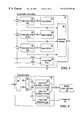
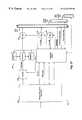
- FIG. 2is a top-level block diagram of a video distribution system according to the present invention.
- FIG. 3provides a more detailed view of the block diagram of FIG. 2;
- FIG. 4is generally a block diagram of the block labelled “A/D” in FIG. 3;
- FIG. 5is generally a block diagram of one of the blocks labelled “Frame Buffer” in FIG. 3;
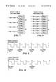
- FIG. 6is generally a block diagram of one of the blocks labelled “Data Gate Array” in FIG. 5;
- FIG. 7illustrates data distribution during data gate array register loading for data driving an active matrix display
- FIG. 8illustrates data distribution during data gate array register loading for data driving a passive matrix display
- FIG. 9illustrates the timing of data transfer within the data gate array of FIG. 6 for data driving an active matrix display
- FIG. 10illustrates the timing of data transfer within the data gate array of FIG. 6 for data driving a passive matrix display
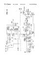
- FIG. 11illustrates the Analog Front End of FIG. 4
- FIG. 12illustrates back porch clamp timing
- FIG. 13illustrates the function of the A/D of FIG. 4
- FIG. 14is an equivalent circuit of the phase fine tune block of FIG. 4;
- FIG. 15illustrates interconnected switches employed in the video clock regenerator circuit of FIG. 4;
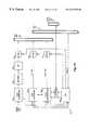
- FIG. 16is a schematic of a switching DC/DC converter used in the present invention with an integrated charge pump used to supply an auxiliary output;
- FIG. 17is an overview of the connectivity and various interface circuit cards which can be utilized in an exemplary embodiment of a video distribution hub according to the present invention.
- FIG. 18is a block diagram of a system card for use in the hub of the present invention.
- FIG. 19is a block diagram of an analog input card for use in the hub of the present invention.
- FIG. 20is a block diagram of a computer overlay input card for use in the hub of the present invention.
- FIG. 21is a block diagram of a broadcast video input card for use in the hub of the present invention.
- FIG. 22is a block diagram of a data exchange card for use in the hub of the present invention.
- FIG. 23is a block diagram of a PANELLINKTM output card for use in the hub of the present invention.
- FIG. 24is a block diagram of a DFP output card for use in the hub of the present invention.
- FIG. 25is a block diagram of a CRT output card for use in the hub of the present invention.
- FIG. 26is a block diagram of a video display device for use in association with the hub of the present invention.
- a common video graphics adapter for coupling a host computer such as a personal computer (PC) , workstation, microcomputer, minicomputer, mainframe or the like to a video displaytypically provides an “oversize” display buffer which has a buffer capacity greater than that necessary to drive a single, conventionally-sized video display.
- This oversize display buffer and the data contained thereinis illustrated in FIGS. 1A-1D as a large field 10 of video data available for display.
- FIG. 1Ait is desired to take four non-contiguous, horizontally oriented portions 12 a- 12 d from the adapter buffer field 10 and to display them on adjacent display devices.
- FIG. 1Bit is desired to take two vertically-oriented portions 12 e , 12 f from the same video graphics adapter buffer field 10 and to display them on adjacent, vertically-oriented displays.
- a mix of vertically- and horizontally-oriented portions 12 g- 12 jare taken from the same adapter buffer field 10 and are subsequently displayed with the vertically-oriented portions 12 g , 12 j spatially displaced from the horizontally-oriented portions 12 h- 12 i .
- two horizontally-oriented portions 12 k , 12 lare taken from the same buffer field 10 and are then displayed on adjacent displays. In the latter case, each portion has a common, overlapping region 14 of video information.
- the present inventionenables the simultaneous replication of multiple portions of a single oversize display buffer.
- the prior artrequires the use of multiple video graphics adapters, each providing a buffer field for sourcing a respective buffer portion, particularly in the situation of FIG. 1D in which two portions to be displayed share a common region 14 of video information.
- the typical prior art video graphics adaptercan also be used to provide video data to plural displays, however, the image displayed on each is the same.
- a host computer 16provides input data to a video graphics adapter (VGA) 18 via a host computer interface such as a PCI bus.
- VGA 18is typically a circuit board installed within the host computer 16 , though other physical embodiments and placements are envisaged.
- the graphics adapter 18is used to generate text and graphical video data from the input data, and to make such video data available to display devices in an internal video display buffer.
- the digital video data in the video display bufferis converted by the VGA 18 to an analog signal comprised of components for each of the fundamental colors employed by conventional display devices, red, green and blue (RGB).
- RGBred, green and blue
- the video data in the video display bufferis received by a video distribution hub 20 via a video cable 22 .
- horizontal sync (HSYNC) and vertical sync (VSYNC)are derived locally in the hub 20 from the analog RGB video data and/or through additional sync signals conveyed through the video data cable 22 , as discussed subsequently.
- the video cable 22also provides a DDC (display data channel) bus, a VESA (Video Electronics Standards Association) standard bus, for the purpose of enabling configuration control between the host computer 16 and the hub 20 .
- the video cable 22provides a USB (Universal Serial Bus) connection between the host computer 16 and the hub 20 , also for the purpose of configuration control.
- USB connectionsare for future expansion and are terminated in a resistor pad found in conjunction with frame buffer circuitry, discussed subsequently.
- the hub 20is comprised of two major circuit blocks, an analog-to-digital (A/D) front end 24 , and plural frame buffers 26 .
- the A/D section 24converts the color data for each of the RGB colors into a digital representation, and provides temporary storage for this digital data.
- the hubis an enclosure having approximate dimensions of seven inches in width, one inch in height, and nine inches in length, though other hub embodiments assume other relative and absolute dimensions. Heat relief is provided as required.
- Physical interfacesinclude an input port for receiving the RGB video stream over the video cable 22 , a power supply connection for interfacing to a +12 V unregulated (or regulated) power supply (not shown) , and output ports for each frame buffer 26 enabling interconnection of the display device cable 30 .
- LAN portssuch as a BNC connector and RJ45 connector, enabling intercommunication between plural hubs are also provided in one embodiment.
- a serial portis also provided, enabling a remote host (not necessarily the same host as that which houses the respective video graphics adapter) to provide command and control data to the hub, and to return data. This serial link can be used, for instance, to command the hub to initiate communication over the LAN with other LAN-connected hubs. In an exemplary embodiment, this serial port is an RS232 port.
- the A/D section 24 and two of the frame buffers 26are disposed on a first circuit card within the hub 20 .
- Two further frame buffers 26are located on a separate circuit card, also within the hub 20 .
- up to eight frame buffersare supported within the hub, all interfacing through a single A/D 24 . Physical dimensions for such a hub 20 would of course be adjusted to accommodate the additional circuit cards.
- the present inventionis discussed at a more detailed level with respect to FIG. 3 .
- the video display buffer 32otherwise known as a large frame buffer, is illustrated in association with the video graphics card 18 .
- the RGB video datais illustrated as being conveyed from the video graphics card 18 to the hub 20 , and in particular to the A/D section 24 . Further detail on the A/D section is presented below.
- this parallel busis 48 bits wide; there are eight bits per pixel per each of the three colors, or twenty-four bits per pixel, and it is desired to transmit two pixels per clock cycle.
- Over this bus 34flows all of the digitized video data which corresponds to the complete contents of the video display large frame buffer 32 as received by the A/D section 24 . It is within the frame buffer 26 logic that the determination of where to begin storing data and where to stop is made. By starting and stopping the storage of video data, each frame buffer section 26 is capable of providing to the respective video head 28 only that portion 12 of the total video display buffer 32 which is desired.
- the frame buffers 26are each illustrated as being comprised of a logic section 36 and an SGRAM (synchronous graphics RAM) 40 .
- the logic 36is responsible for storing in the SGRAM 40 only video data associated with the video buffer portion 12 desired to be displayed on the respective display device 28 .
- the SGRAM 40provides temporary storage of this data to enable the timely provision of the data to the respective head 28 .
- An analog front end 42 ACcouples the received analog RGB signal from the video cable 22 .
- the video signal for each coloris approximately 0.7 Vpp, from the darkest to lightest extremes. Therefore, it is necessary for the analog front end 42 to amplify the video signal for each color, thus improving the signal to noise ratio (SNR) of the following A/D converters (ADCs) 50 .
- Suitable video preamps for this purposeinclude the National LM 1205 and LM 1283.
- Gain control for these amplifierscan be either fixed or variable, depending upon the embodiment. Most simply, the gain control is fixed by the factory. In a further variant, the gain control is fixed in the factory, though the user has physical access to a gain control adjusting means.
- the gain controlis variable and is controlled by a control circuit 44 in the A/D section 24 having a digital to analog converter (DAC) for generation of the control signal.
- DACdigital to analog converter
- An appropriate D/A for this purposeis the Analog Devices AD8403AR10.
- the gain control(also referred to as contrast control) is adjusted jointly for all three amplifiers (i.e. each of RGB).
- One A/D per coloris employed in the embodiment of the present invention.
- An alternative embodimentemploys pixel merging due to the compression afforded by this technique. Pixel interleaving is described in commonly assigned U.S. patent application Ser. No. 08/538,116 entitled “Video Interface System Utilizing Reduced Frequency Video Signal Processing,” incorporated herein by reference.
- two A/Ds per colorare used for video rates above 75 MHz.
- a back porch clampis employed for the purpose of clamping the amplified input signal to a known reference during a clamp interval, and is illustrated in FIG. 12 .
- Other clamping or DC restore techniquescan be employed.
- a suitable device for the A/Ds 50includes the Philips TDA8714.
- six bitsare employed for color representation. The choice hinges upon desired (or required) color depth.
- the eight-bit video data representations per colorare clocked into two banks of pixel bus buffers 54 .
- One pixel's worth of datais clocked into one bank of buffers 54 on even pixel clock cycles, while another pixel's worth of data is clocked into the other bank of buffers 54 on odd pixel clock cycles.
- Suitable buffers for this functioninclude 74LVT574SM chips from Texas Instruments.
- a sync processor 46such as a Mitsubishi M52347SP.
- Outputs of the sync processorinclude: HSYNC+ and VSYNC+, correlating to HSYNC and VSYNC signal timings, respectively; CLAMP+, used by the analog front end 42 in timing the DC restore, as previously discussed; and status bits usable by local processing to indicate what sync type was input to the sync processor 46 .
- HSYNC+is used as an input to a phase fine tune (PFT) circuit 48 .
- the PFT 48adjusts where the video signal is sampled by the ADC 50 within a pixel lifetime by employing an adjustable delay of HSYNC+.
- the output of an RC charging circuitsuch as that shown in FIG. 14 is compared, using for instance an Analog Devices AD9696, with a control voltage generated by the control circuit 44 in the generation of H(pft)+.
- An external adjustmentsuch as an encoder is provided on the exterior of the hub 20 chassis to enable manual adjustment of the control voltage, in an illustrative embodiment.
- Other encodersexist, such as those on the attached heads 28 . The state of these encoders is also reported back to the control circuit 44 . Therefore, the present invention is responsive to adjustment of PFT at either a central location such as the hub, or remotely, such as at the heads.
- a video clock regenerator circuit 52including a fully programmable clock regenerator such as an ICS1522 made by Integrated Circuit Systems, Inc., a phase locked loop (PLL) frequency synthesizer.
- the clock regeneratoris serially programmed in a preferred embodiment of the present invention by the control circuit 44 to generate four clock outputs, each at 1 ⁇ 4 the sampled pixel rate and 90 degrees out of phase with the following output, which collectively comprise a clock at the sampled pixel rate.
- Various frequenciesare employed, depending upon the video data rate. For illustrative purposes, 75 MHz is used herein.
- the clock regenerator circuit 52is comprised of a MOSFET bus switch, such as a Texas Instruments 74CBT3125 quad bus switch.
- MOSFET bus switchsuch as a Texas Instruments 74CBT3125 quad bus switch.
- the purpose of the MOSFET bus switchis to generate two 75/2 MHz clocks, 180 degrees out of phase with other, from the four 75/4 MHz staggered clock signals from the clock regenerator/frequency synthesizer.
- Each switchis a MOSFET switch having an inverted-input output-enable associated therewith.
- the first clock signal from the clock regeneratoris fed to the input of the first switch, and the second clock signal, 90 degrees out of phase (lagging) with the first clock signal, is connected to the output enable for the first switch.
- the third and fourth clock signalsare connected to the second switch in a similar manner.
- the outputs of the first two switchesare then tied together, providing an output clock with clean rising edges due to the speed of the switches and having a period of 75/2 MHz.
- clock twois connected to the input of switch three, and clock three is connected to the output enable of switch three.
- Clock fouris connected to the input of switch four, and clock one is connected to the output enable of switch four.
- the outputs of switches three and fourare also tied together. The resulting output is also a 75/2 MHz clock signal, though 180 degrees out of phase with the output from the first two switches.
- Each of the 75/2 MHz outputs from the bus switchare used to clock a respective PLL clock driver such as the CDC536 from Texas Instruments as part of the video clock regenerator 52 .
- This partenables the generation of a doubled output, a 75 MHz clock also referred to as the ADCLK or “dot clock”, which is used to clock the ADCs 50 .
- other frequenciesare employable as required.
- the clock driverprovides 75/2 MHz clocks (“PCLK/2+” and “PCLK/2 ⁇ ”) of like phase with respect to the clocks from which they are derived.
- Such clocksare used to clock the pixel bus buffers 54 latching digital video data out of the ADCs 50 , since data gate arrays in the frame buffer logic 36 can't run at speeds such as 75 MHz (data gate arrays are discussed later).
- the sampling ratedoes not exceed 75 MHz, with the limitation being found in the analog preamplifier of the analog front end 42 and in the speed of the ADCs 50 .
- the clock regenerator circuit 52also enables the regeneration of HSYNC, in a form referred to as LOCHSYNC, or local HSYNC, even without an external HSYNC.
- LOCHSYNCis employed by the control circuit 44 in controlling the output of the frame buffers 26 .
- the on-screen display chip(not illustrated) is employed in the A/D circuit block 24 , and specifically, in conjunction with the analog front end 42 . Analog output from this chip is mixed into the A/Ds 50 . A single user interface to this chip is provided.
- control over when and for what duration a frame buffer 26 captures video dataresides within the A/D circuit block 24 , and in particular within the video clock regenerator 52 using gating signals.
- control over when and for what duration a frame buffer 26 captures video dataresides within the A/D circuit block 24 , and in particular within the video clock regenerator 52 using gating signals.
- signalswould only gate one frame buffer 26 , such embodiment is not preferred.
- the control circuit 44provides a VSYNC disable to the video clock regenerator 52 to disable the PLL during vertical intervals. Otherwise, spikes generated by the PLL in the vertical interval would cause errors in forward error correction.
- control circuit 44 in the A/D circuit block 24Functions of the control circuit 44 in the A/D circuit block 24 have previously been alluded to, such as the generation of the analog preamplifier gain control, creation of VControl for use in the PFT 48 , generation of the Vsync disable and serial data signals for use in the video clock regenerator 52 .
- the control circuitcomprises in a preferred embodiment the following elements.
- a DACis required in the generation of amplifier gain control.
- Other elements comprising the control circuitinclude a serially programmable digital potentiometer, such as an Analog Devices AD8403AR10, which enables the generation of A/D circuit-internal control signals such as: CONTRAST, an adjustment to the video preamp in the analog front end 42 ; CLAMP_WDTH, used in the sync signal processor; and the PFT control signal previously discussed.
- control circuit 44is comprised of a C25 microprocessor with an XC5202 microprocessor gate array.
- Principal signals received by the control circuit 44include clocks from the video clock regenerator 52 , and HSYNC+ and VSYNC+ from the sync processor 46 .
- clocks from the video clock regenerator 52and HSYNC+ and VSYNC+ from the sync processor 46 .
- HSYNC+ and VSYNC+from the sync processor 46 .
- a serial PROM and a parallel EEPROMprovide data to the gate array and microprocessor, respectively.
- the use of the parallel EEPROMenables the reprogrammability of the hub.
- the microprocessor and associated gate arrayare in communication with devices external to the hub 20 via a serial port disposed on one end of the hub 20 .
- a UARTuniversal asynchronous receiver/transmitter
- TL16C550ATL16C550A
- TTL to EIA level translatorsuch as an MAX211E
- the control circuitis also in communication with devices external to the hub 20 through LAN ports, such as BNC or RJ45 connectors.
- Standard LAN interfacesare employed in a preferred embodiment, such as an SMC91C94 LAN chip, coupled to a DP8392 encoder.
- Such a LAN interfaceenables programmability of the hub 20 as an addressable port on a LAN shared by devices other than hubs, or as a port on a LAN dedicated solely to one or more hubs in communication with a configuring device or devices. In either case, the hub 20 is a “dumb” device which only responds when directed to from an intelligent device.
- the serial communicationcan be either 10Base2 or 10BaseT.
- a DDC busenables configuration of the hub 20 by the host computer 16 .
- This busis comprised of two data signals, SDA (serial data) and SCL (serial clock), +5 VDC, and return.
- SDAserial data
- SCLserial clock
- +5 VDCreturn.
- the DDC channelis normally employed, in the prior art, as a unidirectional pathway to a repository of peripheral device configuration information available to a host.
- the C25 processorreads and writes the DDC memory dynamically with information pertaining to the configuration of the hub and the attached heads.
- the DDC memorywhich can be discrete or part of the control circuit memory, is then read by a host.
- control circuitcan be configured, or reconfigured, via internal replacement of programmed memory devices, external communication to removable configuring devices such as via a LAN interface, or by input from the host computer.
- configuration informationcan include, explicitly or implicitly, the point (row and pixel) within the frame at which each displayed segment is to begin.
- digital video datais provided in parallel as eight bits per color per pixel, with two pixels being provided per clock cycle, for a total of 48 bits.
- Other signals which are provided by the A/D circuit block 24include: USB signals, which are for future expansion in the present embodiment and are therefore terminated at a daughter board connector proximate the frame buffer circuitry; horizontal and vertical sync signals from the sync signal processor 46 ; various clock signals originating in the video clock regenerator 52 ; a start of frame signal generated by the control circuit 44 from the horizontal and vertical syncs; and serial control data also generated by the control circuit 44 .
- One frame buffer circuit block 26is illustrated in FIG. 5 at a first order of detail, bearing in mind that there are up to four frame buffer circuit blocks 26 in each hub in a first embodiment, each capable of providing digital video data to a respective display head 28 .
- Sixteen parallel bits of video data per colorare received by a respective data gate array 56 .
- the data gate array 56enables the storage of the video data in the respective SGRAM 40 if the data is part of the desired portion 12 of the video display buffer in the VGA 18 , based upon control received from an associated control gate array 58 .
- there is one control gate array 58 per frame buffer logic circuit 36though in an alternative embodiment, one control gate array 58 is shared between two frame buffer logic circuits 36 .
- the datais stored in the respective, single-ported SGRAM 40 .
- the datais then removed from the SGRAM 40 where it passes again through the data gate array 56 to the PANELLINKTM 60 , the latter acting as an output interface to the associated head 28 .
- FIG. 6provides an illustration of a data gate array 56 and an associated SGRAM 40 for a single color channel.
- Video data input to the data gate array 56 for one of the three colors, two parallel eight-bit pixels,is received on sixteen parallel signal paths at approximately 80 MPixels/sec (or 40 MPixelPairs/sec) within a demux 63 in the data gate array 56 .
- This demux 63enables the distribution of the input data into two sixteen bit registers 64 , which in turn provide thirty-two bit parallel data to a 32 bit wide, 16 bit deep write FIFO 66 .
- the data is transferred into the registers 64depends upon the type of head 28 associated with this color channel as conveyed by the head 28 to the control circuit 44 (via the DDC backchannel) through the serial port to the control gate array 58 (on a separate serial bus).
- all eight bits per pixelare utilized.
- the upper of the two registers 64is filled with four four-bit nibbles during clock cycle zero, representing two eight-bit pixels for this color.
- clock cycle onetwo more pixels are loaded into the lower sixteen-bit register 64 .
- clock cycle twothe 32 bits of data representing four pixels for this color are clocked into the write FIFO 66 and the upper register 64 is written with the next two pixels.
- the clock speed into the write FIFO 66is 20 MHz for active matrix displays in the first embodiment of the present invention. Other exemplary embodiments employ other clock speeds.
- the associated head 28is a passive matrix display
- the lower four bits of each eight bit pixelare dropped and the upper four bits are clocked into the registers 64 as indicated in FIGS. 8 and 10.
- the upper four bits for each pixelare stored in respective portions of the registers 64 , while the lower four bits are dropped.
- the data in the registers 64are clocked out to the write FIFO 66 and the process of receiving the upper four bits per pixel in the registers 64 begins again.
- the clock speed into the write FIFO 66 for passive matrix displaysis 10 MHz.
- the output of the write FIFO 66is connected to a 32-bit data path. Also connected to this data path are the respective single-ported SGRAM 40 , which is 32 bits wide by 256 kbytes deep, and a read FIFO 68 of the same dimensions as the write FIFO 66 .
- a suitable SGRAM 40 for this applicationis an IBM038329N06A-10, which operates at 50 MHz. Desired video buffer portion 12 data from the write FIFO 66 is read into the SGRAM 40 under the control of the control gate array 58 .
- data out of the write FIFO 66is written to the SGRAM 40 for eight clock cycles, the 32-bit wide bus is idle for two clock cycles, data is read out of the SGRAM 40 and into the read FIFO 68 for eight clock cycles, then the bus goes idle for another two clock cycles.
- the desired portion 12 datacan be any contiguous portion of the video buffer data from the video graphics adapter 18 in the host computer 16 , limited maximally in size by the characteristics of the associated head 28 .
- control circuit 44 in the A/D circuit block 24provides the control gate array 58 in the frame buffer logic block 26 with horizontal and vertical offsets, relative to the start of frame notification, via the serial data path between the two for the commencement of data storage in the SGRAM 40 . These offsets are used to control a video microsequencer implemented in the control gate array 58 for enabling the transfer of digital video data into the video registers 64 , and subsequently into the write FIFO 66 .
- a memory controlleralso implemented in the control gate array 58 , controls the transfer of data from the write FIFO 66 to the SGRAM 40 , and from the SGRAM 40 to the read FIFO 68 .
- a panel microsequenceragain, implemented in the control gate array 58 , controls the output of data from the read FIFO 68 to Frame Rate Modulation (FRM) logic 70 (discussed subsequently).
- FFMFrame Rate Modulation
- the programming of the video microsequencer with the offset informationis preferred due to the ease of adjusting the offset values when a respective head is replaced or when the display characteristics for a head are changed. How much data to store is calculated by the control circuit 44 based upon display size, resolution, and orientation as learned from the respective head 28 via the DDC backchannel.
- the frame signalis used for interlaced video applications, the control gate array 58 using this signal to identify even versus odd frames.
- data storage in the SGRAM 40is solely under the control of the control circuit 44 , the latter sending the equivalent of “on” and “off” signals to the control gate array 58 .
- a drawback of such controllies in the need for separate control lines between the control circuit 44 and each control gate array 58 .
- control circuit 44provides “on” signals to the control gate array 58 , and the control gate array 58 provides the “off” signal based upon backchannel information relating to the associated head 28 .
- the multiplicity of control signalsis once again a drawback of this embodiment.
- the memory controllertracks the data flowing into and out of the FIFOs 66 , 68 and the SGRAM 40 . If the write FIFO 66 is less than half full, a write to the SGRAM 40 from the write FIFO 66 is disabled; if the read FIFO 68 is more than half full, the SGRAM 40 is prevented from writing to the read FIFO 68 .
- the bus intermediate the FIFOs 66 , 68 and the SGRAM 40remains idle during the clock cycles which would otherwise be used for writing data from or reading data to the SGRAM 40 .
- FRMframe rate modulation logic circuit
- PANELLINKTM 60associated with that frame buffer 26 (there is one PANELLINKTM 60 per frame buffer 26 ).
- the FRM 70executes an algorithm which reserializes the input data by taking the four, eight-bit wide pixels, buffering them, and outputting the data as sequential eight-bit wide pixel data.
- the maximum input rate into the PANELLINKTM from the FRM 70is up to 65 MHz in the present embodiment.
- the FRM 70executes a conversion algorithm which also receives 32 parallel bits, but in the form of eight, four-bit pixels.
- the algorithmconverts the four bit pixels into one-bit pixels using frame rate modulation. This involves the use of a look-up table in the FRM 70 and the frame number which is passed from the A/D control circuit 44 to the control gate array 58 to the FRM 70 .
- the algorithmeffectively averages the color of the same pixel over time, and compares the possible values for this pixel against that of surrounding pixels to enable the use of one-bit per pixel with minimized visual artifacts.
- the output of the FRM 70 for an associated passive matrix displayis eight parallel one-bit pixels. Alternatively, any suitable FRM technique may be employed.
- the data format for an associated passive matrix displaycould be four eight-bit pixels in parallel into the FRM 70 , instead of the current eight four-bit pixels.
- the frame rateis twice that of the active matrix display. Typical values are 120 Hz frame rate for a passive matrix display versus 60 Hz for an active matrix display.
- the chief advantage of passive matrix displaysis cost; presently, such passive displays cost roughly one-third the cost of active matrix displays.
- An active matrix displaymay take two pixels per clock cycle, in order.
- a “dual scan passive” displayprovides four one-bit pixels per clock cycle at both a top and bottom half of a display. Thus the difference in frame rate.
- the PANELLINKTM 60receives eight bits per pixel per color, or 24 bits per pixel total, at up to 65 MHz for an associated active matrix panel head 28 , four times the FRM 70 input clock rate.
- the PANELLINKTM 60receives pixel data for an associated passive matrix display at approximately 20 MHz, the same as the input rate into the FRM 70 .
- the PANELLINKTM 60such as a Chips & Technologies 65100, formats the input data for provision to the respective head 28 . It receives the three eight-bit data streams from the FRMs 70 , one for each color, and using the HSYNC and VSYNC signals from the A/D control circuit 44 via the control gate array 58 formats the data for output over four differential lines at a connector to the respective head 28 .
- the PANELLINKTMprovides its outputs to the respective head 28 over the display device cable 30 as four twisted pairs.
- This cable 30also provides 12V power and ground, a USB backchannel (the latter not being employed in the present embodiment), and the DDC backchannel to the control circuit 40 .
- Four of the twisted pairsare for the RGB data and data clock.
- One twisted pairis for the DDC backchannel.
- Another twisted pairis for the USB.
- Each of the USB and DDC backchannelsprovide individual data and clock paths, and share 5V, 12V and ground which are also conveyed in this cable to the respective head 28 .
- Other elements of the presently disclosed hub 20include registers which preserve the setup information of the PANELLINKTM 60 , data gate array 56 , and other elements, as received from the control circuit 44 .
- the power requirements for the present hub 20are unregulated 12 VDC. This is supplied to DC/DC converters which generate 5V and 3.3V for use as logic supplies.
- the unregulated 12 VDCis used as an input to an analog power and control circuit which includes a switching DC/DC converter 72 , as shown in FIG. 16 .
- the 12 VDCis applied to a buck switching regulator drive 74 .
- This drivecan take many forms, such as a switching regulator (e.g. a Linear Technology LT1376), or a regulator controller.
- This drive 74essentially a 12 Vpp rectangular wave, is coupled through an inductor 80 to a filter capacitor (or capacitors) 82 at the output of the inductor 80 in the common buck configuration, to supply 5 VDC for use in the analog section.
- the output of the regulator drive 74is also employed to drive a charge pump providing a higher-voltage input to an auxiliary DC supply circuit, generally designated 84 in FIG. 16 .
- This circuit 84includes alternately-conducting diodes 86 , and one or more reservoir capacitors 88 coupled to a micropower low dropout regulator (e.g. a Linear Technology LT1129) 90 , effectively providing a regulated, auxiliary 12 VDC output. Other voltages can be generated, depending upon system requirements.
- a micropower low dropout regulatore.g. a Linear Technology LT1129
- the hub 20is configured to accept a digital video input.
- the data gate array 56 in this embodimentis configured to properly format the input digital data prior to its processing by the write FIFO 66 , the SGRAM 40 , the read FIFO 68 , the FRM 70 , and the PANELLINKTM 60 .
- Such a hub 20can be configured to accept either analog data input as previously described or digital data input, or can accept just digital data, eliminating some of the cost of the circuitry associated with the analog front end in the A/D circuit block 24 .
- bufferssuch as the pixel bus buffers 54 are employed to temporarily hold the digital data prior to processing by the data gate array 56 .
- the digital output of the hubis employed as a digital input to one or more subsequent hubs.
- the PANELLINKTM interface 60can also be replaced with D/A converters. Such an embodiment could then drive conventional CRTs, or could provide analog input to one or more subsequent hubs.
- the inputs and outputs of the hub 20can be adapted to receive and/or transmit data in an optical format.
- a configurable hubwhich enables the merging of plural, disparate video inputs into a single pixel bus dataset, and the selective display of independent portions of that dataset on one or more display devices which themselves may have disparate input requirements.
- the configurable video hub of FIG. 17illustrates a number of integrated circuit cards in mutual communication. Each of the cards will be discussed in detail subsequently.
- the purpose of the hub and cards installed thereinis to accept base image data and/or data for one or more overlay images via input interface cards.
- the base image dataif any, defines the outer bounds of a video display dataset and is driven onto a pixel bus 114 and merged with the overlay image data, if any.
- no overlay dataexists and the resulting pixel bus dataset is comprised only of base image data.
- the base image datais completely replaced by overlay data. In between these extremes, the overlay data may appear as a window of overlay data amidst the base image.
- the base imagemay not be driven onto the pixel bus at all, such that the overlay data is driven onto the pixel bus amidst a default video display value representing the area the base image would otherwise occupy.
- this default valueresults in the display of a black pixel within the base image field in each location where an overlay pixel is not merged.
- a system card 110is installed in each hub for control purposes, as described below. It is also capable of receiving input data in the PANELLINKTM format for use as the base image. Other input cards may also be used, though the hub can function in one embodiment with a system card and up to five output cards.
- Pixel datais driven onto a pixel bus 114 for subsequent extraction from the pixel bus 114 by one or more output interface cards.
- Each output interface cardthen either forwards the entirety of the extracted pixel bus data to one or more interconnected video display devices, or forwards a specific portion of the pixel data to an interconnected display device.
- that deviceis provided with a frame buffer for selectively extracting a portion of the entire pixel bus dataset for display.
- a hub chassisthere are six card slots in a hub chassis, one of which is occupied by a system card 110 , as illustrated in FIG. 18 .
- the five remaining slotsare available for interfacing to a variety of video input sources and a variety of output display devices.
- Other hub embodimentsprovide a smaller or larger number of card slots.
- the hubalso provides a backplane for supporting a CPU bus 112 , a serial control bus 113 from a system card CPU 126 , the parallel pixel bus 114 , a gate array serial bus 115 and a power supply module (not shown).
- the CPU bus 112is comprised of sixteen data and eight address lines to and from the system card CPU 126 , a write/read control bit for addressing gate arrays on other interface cards, and a per slot enable line for each of the hub slots.
- the serial control bus 113is comprised of a clock line and a data line from the CPU 126 , and is used for writing to and reading from control registers disposed throughout the hub and for writing to and reading from registers associated with frame buffers which may be disposed in association with display devices external to the hub.
- the pixel bus 114comprises parallel data lines which are one pixel (twenty-four bits) wide, in addition to horizontal synchronization (HSYNC), vertical synchronization (VSYNC), data enable (DE), a pixel clock line for each hub slot 124 , and an overlay control line (inverse-OVERLAY).
- the latter signalis asserted by an input interface card while it is driving an overlay signal onto the pixel bus, as described subsequently.
- the pixel bus 114also supports a common pixel clock line 123 driven by the input interface card providing a base image signal in the absence of such a base image signal input to the system card 110 .
- a first embodiment of the power supply modulereceives twelve volts, regulated or unregulated, and outputs 3.3 volts and 5.0 volts on the backplane.
- the CPU 126is capable of determining the power requirements of the cards populating the hub, and of associated display devices which rely upon the hub for their power.
- the CPU 126is also capable of selectively enabling and disabling certain electronic elements if there exists insufficient power. For instance, the CPU 126 is capable of deactivating a frame buffer of a particular interface card, an element which tends to consume more power than others, should power requirements exceed capacity.
- Each hubcontains a system card 110 , such as shown in FIG. 18 .
- Digital video data in PANELLINKTM formatcan be provided as the base image to the system card 110 via a standard PANELLINKTM interface unit 116 .
- the output of this interface 116is pixel data (DATA), HSYNC (H), VSYNC (V), and a data enable indication (DE), all of which are buffered in registers 118 under the control of a gate array 120 .
- the PANELLINKTM interface 116if receiving a PANELLINKTM video signal, also derives a pixel clock from the input signal for distribution throughout the hub via clock distribution logic 122 .
- the base image datawill be output to the pixel bus all the time in the absence of overlay data from one of the other input interface cards disposed within the hub.
- the gate array 120 control logic on the system cardenables the registers 118 in communication with the PANELLINKTM interface 116 .
- the system card gate array 120 , CPU 126 and associated circuitrycollectively comprising the CONTROL block 111 shown in FIG. 18
- the gate array 120in response to initiation of the inverse-OVERLAY signal by the overlay card, disables the system card pixel bus registers 118 while the overlay data is being written to the pixel bus 114 by another input card.
- the clock distribution logicreceives a clock 123 from one of the other input cards installed in the hub. In any case, under the switch control of the gate array 120 , the clock regeneration logic 122 then provides the pixel clock signal directly to the gate array 120 of the system card 110 and to each of the remaining interface cards installed in the hub via discrete clock lines 124 .
- the system card gate array 120(executing software stored in associated memory 128 ) selects one of the overlay input signals from one of the other input cards as a source of pixel clock and sync signals. The choice of which is used for this purpose may be made based upon pixel clock speed, card slot position, or some other factor.
- a local area network (LAN) interface 130provided in association with the gate array 120 of the system card control block 111 provides an interface for a serial control line input, such as a 10BaseT interface.
- a serial control line inputsuch as a 10BaseT interface.
- This inputis utilized to program the memory 128 utilized by the gate array 120 and the CPU 126 in configuring the interface cards of the hub. For instance, it is through this path that overlay windows are defined in the hub.
- the interfaced computerrelays to the hub that a window is to be established at certain screen coordinates; the hub then configures the appropriate input overlay card to begin driving pixel data onto the pixel bus at the appropriate time such that the window defined by the computer is provided.
- the memory 128itself is preferably comprised of a combination of a high-speed flash memory and a RAM scratch pad area.
- the flash memory portionis utilized for parameter storage, which is the hub configuration and source characterization information, and a non-volatile code space is provided for the CPU 126 .
- the system card control block 111further comprises a universal asynchronous receiver/transmitter (UART) 132 , also for the purpose of providing a serial port interface to the control block 111 .
- UARTuniversal asynchronous receiver/transmitter
- the UART 132is replaced with a universal serial bus (USB) interface, which has the capability of providing extra ports, should the need arise, through the use of an expander. Either serial interface enables the same type of overlay control exercised using the LAN interface, as previously described.
- One of the functions which the control block 111 performsis to analyze the received HSYNC and VSYNC from a video input, received by any of the input interface cards, for the purpose of identifying the source of the video signal. These signals are provided to the gate array 120 via receivers 134 in communication with the pixel bus 114 . For instance, different video sources use three common video sync protocols, as previously described. Such source identification information is useful in determining how large a frame the source can provide. The source information is also utilized when the system card gate array 20 is programming the new base image card.
- an analog input card 140is illustrated.
- a standard video connector 142is provided to interface the hub to the source of analog video data, such as the RGB output from a standard personal computer graphics adapter card.
- the received datais buffered by an analog buffer 144 prior to being passed through an analog-to-digital converter 146 , such as that illustrated in the A/D circuit block 24 of the video distribution hub, above.
- registers 148under local control, are utilized to gate the digitized video data onto the pixel bus. The data will be driven onto the pixel bus 114 when this analog input card is the base image card, and the base image is not being overlaid.
- the video connector 142also provides an input to a sync separation block 150 for the purpose of identifying the input data format and isolating the HSYNC and VSYNC from the analog input signal. These sync signals are also gated to the pixel bus 114 via registers 148 for source identification by the system card 110 .
- the video connector outputis driven to a clock regeneration unit 152 for the purpose of extracting a pixel clock from the received data in the case when the analog input signal is utilized in the hub as the base image or default source of reference timing. Whether the locally recovered pixel clock is provided to the remainder of the hub interface cards is controlled by a switch 154 , which is in turn controlled by local control logic 156 .
- this local control logic 156is implemented in a programmable array logic (PAL) unit, which includes one or more register interfaces controlled by the CPU bus 112 .
- PALprogrammable array logic
- Other embodimentsutilize specialized registers for this purpose.
- the control logic 156programmed by the system card 110 CPU 126 via the CPU bus 112 , performs the simple control functions related to enabling pixel data output to the pixel bus, outputting the locally recovered HSYNC, VSYNC and DE onto the pixel bus, and forwarding the locally recovered pixel clock to the system card clock regeneration unit 122 .
- FIG. 20Another input interface card which can be employed in the hub is a computer overlay input card 160 , as shown in FIG. 20 .
- this cardresembles the analog input card 140 of FIG. 19 .
- bothemploy a video connector 142 , 162 as an interface to an analog input signal.
- Bothbuffer the received video data with a buffer element 144 , 164 , and both send the received analog data through an analog-to-digital converter 146 , 166 .
- the computer overlay input card 160also employs a control gate array 168 and associated sync separation block 170 and a clock regeneration unit 172 which, while analogous to the local control logic 156 and associated elements of the analog input card 140 from a macroscopic view, actually provide a more complex level of control over the received analog video data. This heightened level of control is necessary in order to control the output of at least a portion of the received analog video data onto the pixel bus as an overlay, as described below.
- the memory in the computer overlay input card 160is a frame buffer implemented with a form of “ping pang” memory 174 , comprised of two memory banks identified as MEMORY 0 and MEMORY 1 in FIG. 20, where data coming into and out of the memory 174 passes through a central data switch labelled SWITCH.
- SWITCHcentral data switch
- the control logic for the computer overlay input cardemploys a control gate array 168 in a first embodiment which acts as a microsequencer.
- the memory switchis under the control of the gate array, as is the sync separation block 170 and the clock regeneration unit 172 , whose outputs are used in order to time the writing to the memory banks.
- the control gate array 168indicates to the sync separation block 170 and the clock regeneration unit 172 what format the received data is in for the purpose of recovering the syncs, DE and pixel clock. This data is then made available to the system card, including line count and frame time, for software source recognition.
- Received analog video datais selectively buffered in the memory banks of the memory 174 , and is gated to the pixel bus 114 by registers 175 . Both operations are under the control of the control gate array 168 .
- the gate array 168is programmed by the system card 110 via the serial control bus to identify a starting point and an offset within the buffered data for when the overlay data is to commence.
- the serial control bus from the system cardis also used to program the computer overlay input card to specify the portion of overlay data stored in the frame buffer 174 that is to be output to the pixel bus 114 , and the point within the pixel bus frame data that the overlay data output is to commence.
- the gate arrayasserts the inverse-OVERLAY signal. This signal alerts the input card generating the base image that the overlay card is writing data to the pixel bus, and that the base image card should shut off the registers gating the base image to the pixel bus.
- the instructions from the system card to the input overlay card as to what portion of the buffered overlay data is to be written onto the pixel bus at the appropriate timetakes a variety of forms. For instance, overlaid data can be merged into the base image on the pixel bus 114 on a pixel-by-pixel basis, or according to various algorithms pre-programmed into the local control gate array.
- the computer overlay input card 160employs registers 176 for the purpose of either reading in or writing out HSYNC, VSYNC and DE.
- the gate arrayreceives the slot copy of the pixel clock from the system card 110 , or in the case when this computer overlay input card is the base image card, drives to the system card the pixel clock recovered by the clock regeneration block 172 for redistribution to the other interface cards.
- the received pixel clockis required in order to synchronize the output of pixel data onto the pixel bus.
- BVIDEObroadcast video overlay card 180
- This cardis utilized to receive broadcast video data, in one of many formats, to buffer the data in an on-board memory, and to selectively output the buffered video data onto the pixel bus.
- FIG. 21A comparison of FIG. 21 and FIG. 20 reveals that the BVIDEO overlay card 180 resembles the computer input overlay card 160 in many respects.
- Eachhas an input interface specific to the expected data.
- Eachhas a buffer memory for selectively storing the received pixel data, and for enabling the writing of selected portions of that data onto the pixel bus. Further, each has control logic for controlling these functions.
- the BVIDEO overlay card 180uses a broadcast video decoder 182 appropriate for the format of the received video data, which can be in NTSC, PAL, or any other video format.
- This decoderprovides the video data in digital form to a scaler 184 in a first embodiment.
- This scalerselectively reduces the digital pixel dataset, to a degree specified by a user in view of memory capacity and speed, and required resolution at the display device.
- the output of the scaler in this embodimentis then fed to the memory 186 , which is also a “ping pong” memory in a preferred embodiment, as described with respect to the computer overlay input card of FIG. 20 .
- the scaler 184is utilized at the output of the buffer memory 186 , in order to reduce the resolution of a segment of data to be displayed such that a larger overall picture fits into a smaller overlay window.
- the scaling performed by the scaler 184will depend upon the resolution desired in the overlaid window.
- the scaleris therefore programmable by the associated control gate array 188 , whether the scaler is before the memory 186 or after.
- no scaleris utilized.
- control gate array 188 for the BVIDEO overlay card 180is the same as that handled by the control gate array 168 of the computer input overlay card 160 .
- the control gate array 188is responsible for receiving overlay location information and buffer segment to be displayed information from the system card 110 via the serial control lines, for receiving the slot copy of the pixel clock from the system card 110 , for receiving the HYSNC, VSYNC, and DE signals from the system card via registers 190 which it controls, for controlling the function of the ping pong memory switch, and for controlling the registers 192 which gate the pixel data out of the memory 186 onto the pixel bus 114 .
- control gate array 188receives HSYNC, VSYNC, DE and the pixel clock from the broadcast video decoder 182 for enabling source identification carried out by the system card 110 .
- the gate array within the BVIDEO overlay carddrives recovered HSYNC, VSYNC and DE signals onto the Pixel Bus 114 via registers 191 .
- this card 180 and the computer input overlay card 160 -there is no discrete sync separation block or clock separation unit, since those functions are implemented in the broadcast video decoder.
- the video decoder 182is configured for the received video data format by the control gate array, via the serial control buses.
- BVIDEO overlay circuitssuch as that shown in FIG. 21, on a single circuit card.
- Each such circuitemploys the elements shown in FIG. 21 .
- Alternative embodimentsprovide only a single overlay circuit per circuit card, or more than two such circuits per card, depending upon card size and circuit density.
- FIG. 22Another interface card employed in the presently disclosed hub is referred to as a data exchange module 200 , shown in FIG. 22 .
- This moduleenables a user to provide all or a part of the pixel bus data to an interconnected device such as a personal computer or another hub.
- a first memory element 202gated by registers 204 under the control of a local control gate array 206 , provides temporary storage for the desired pixel data prior to being forwarded off board.
- the system card 110and the CPU 126 in particular, is responsible for programming the control gate array 206 of the data exchange module 200 to specify the portion of the pixel data which is desired.
- the data so extractedcan also be provided as an input to another hub as presently disclosed.
- the extracted datawould therefore include any and all overlay data found in the pixel data of the local pixel bus 114 .
- a subsequent hub, receiving such pixel data as an input,would then be configurable such that further overlaid windows could be merged into the pixel data.
- the data out of the data exchange module 200can also be used as an input to a display device, if properly buffered and formatted, such as via a PANELLINKTM interface or any other suitable interface.
- a further feature of the data exchange module 200is the ability to receive pixel data from another source, such as from a corresponding data exchange module in another hub. Such received data is buffered in a second memory element 208 , from which all or a selected portion of the received pixel data can be output onto the pixel bus, under the control of the control gate array 206 as programmed by the system card 110 and using the inverse-OVERLAY signal protocols as discussed above, for instance with respect to the computer input overlay card 160 .
- a data handling element 210Intermediate the two memory elements 202 , 208 and the external device in communication with the data exchange module 200 is a data handling element 210 , which is required in order to transfer data from the synchronous memory elements 202 , 210 to an asynchronous bus in communication with the external device.
- the data handling unit 210is therefore necessary to reformat the pixel data into the desired output format, and its implementation is specified by the equipment to be interfaced to.
- the output of the data handling unit 210can be video, digital or RF in various embodiments.
- the actual interface between the data exchange module 200 and an interconnected device in one embodimentis a LAN/communications (LAN/COMM) circuit 212 , having an associated CPU 214 .
- This interfacecan be configured for interfacing the respective hub to a 100BaseT data path for live video output/input, or to a 10BaseT data path for sending or receiving “snapshots”, or discrete frame samples of pixel data.
- Pixel data captured from the local pixel bus 114can also be routed to the LAN used for configuring the respective hub.
- the desired datais transmitted over the system card CPU bus, which is extended across the hub backplane. From the system card, the data is then routed via the CPU-associated LAN interface 130 to the control LAN.
- the control gate array 206 for the data exchange module 200is also responsible for receiving, or transmitting, HSYNC, VSYNC, and DE via registers 216 .
- the gate array of the data exchange module 200also sets the inverse-OVERLAY signal when data which it has received from an external source is being used as an overlay input to the pixel bus 114 .
- the definition of the overlay from among the received data, the selection of the portion of the overlay data for output to the pixel bus 114 , and the timing of the output of that selected data,is also under the control of the gate array 206 , as programmed by the system card via the serial control buses.
- a further form of input interface cardwhich is not illustrated includes an interface responsive to serial commands for the generation of graphical images. For instance, certain operating system overlays such as X-Windows communicate graphics commands rather than the images themselves. Thus, this interface generates graphics data in response to the received serial commands. These graphics data are then buffered in a frame buffer such as that illustrated with respect to the BVIDEO overlay card.
- a first form of output interfaceis illustrated in FIG. 23, and is referred to as a triple PANELLINKTM output card 220 .
- Data from the pixel bus 114including pixel data, HSYNC, VSYNC, and DE, is captured in a temporary storage element 222 , which depending upon the embodiment can be either registers or a memory buffer.
- the data stored in the storage element 222is then available to the three PANELLINKTM interfaces 224 a , 224 b , 224 c.
- Each PANELLINKTM interface 224 in the triple PANELLINKTM output card 220provides the pixel bus data in PANELLINKTM format along with the sync, data enable, and clock signals. This output is provided to an interconnected display device via a cable which in a first embodiment also provides power to the display device. Connectors 226 adapted for interfacing to such custom cables are provided.
- Each display device connected to the triple PANELLINKTM output card 220has associated therewith a frame buffer for the purpose of storing only the portion of the pixel bus data which is desired for display on the display device.
- the frame bufferthen outputs the desired data for synchronization with a display clock.
- the datais then made available for display.
- the triple PANELLINKTM output card 220also provides a serial control bus 113 link to each interconnected display device for the purpose of programming the display device frame buffer, according to the input provided to the system card 110 by the external control system, with the portion of the pixel data which is to be displayed.
- this datacan be in the format of start and stop signals, or a starting point with an offset to a stopping point, or some other set of controls which identify to the frame buffer what portion of the pixel bus data, via the PANELLINKTM interface, is to be buffered and displayed.
- a register 228is coupled to the CPU bus 112 .
- the register 228is used to control a switch 230 which enables the coupling of the serial control bus 113 and the gat array serial bus 115 to the interconnected display device frame buffers. Since the runs between the hub and each the display devices can be quite long, it would be impractical to try to drive the serial bus to each frame buffer all the time. Further, addressing is not provided at each frame buffer, so there would be no way for a particular frame buffer to distinguish between control signals intended for various frame buffers.
- the switch 230is thus used for selectively routing the serial bus to the appropriate remote frame buffer.
- the triple PANELLINKTM output card 220can be provided with one, two or four or more PANELLINKTM output channels, depending upon space available on the circuit card and the needs of the user.
- FIG. 24Another embodiment of an output interface card for the hub is illustrated in FIG. 24 .
- This cardis the dual DFP output card 240 , which is similar in some respects to the triple PANELLINKTM output card 220 , with the exception that the output of the presently described card is compliant with the DFP standard, and the card includes the frame buffer function on-board, instead of located at the display device as with the display device associated with the triple PANELLINKTM output card 220 of FIG. 23 .
- pixel data from the pixel bus 114is received in temporary storage elements 242 , which can be registers or any other suitable memory element. From there, the buffered data is passed to respective frame buffers 244 which each employ a ping pong memory such as that described in conjunction with the computer overlay input card 160 or the BVIDEO overlay input card 180 .
- This memoryenables the selective writing of pixel data to the dual memory banks, and the reading of stored data at the appropriate time, all under the control of a control gate array 248 , programmed by the system card CPU 126 via the CPU bus 112 and the serial control bus 113 .
- the frame buffers 244are XGA frame buffers, meaning that each has the capacity to buffer enough data from among the entire pixel bus dataset to drive an associated XGA video display device.
- each frame buffer 244is provided to a PANELLINKTM interface 246 for the purpose of sending properly formatted video data to the respective display device.
- the output of one channel of such a dual DFP output card 240can be used as a PANELLINKTM input to, for instance, a system card 110 of another hub, or as an overlay input to another hub.
- the PANELLINKTM interface 246 outputis provided to a standard PANELLINKTM cable connector 250 .
- this output interface card 240provides an extension of the gate array serial bus 115 which is used, depending upon whether the video display device is DDC compliant, for the purpose of collecting data from the display device including technical specifications such as refresh rate of the attached display device, backlight operating time, power conditions, and temperature conditions.
- one or three or more video display channelsare provided, depending upon the availability of circuit card space and the needs of the user.
- a further output interface card employable in the hub of the present inventionis a CRT output card 260 , as depicted in FIG. 25 .
- This cardalso receives pixel bus data in temporary storage 262 such as registers or memory buffers. From there, the received pixel data is sent to memory 264 .
- memory 264employs plural ping pong memories and a switch responding to an associated gate array 268 in order to improve memory bandwidth.
- the gate arrayis programmed by the system card CPU 126 via the serial control bus 113 .
- the output of the memories 264passes through a digital to analog (D/A) converter 266 and is provided to the associated CRT display device via an appropriate connector (not shown).
- D/Adigital to analog
- the gate array serial bus 115 from the gate array 120 of the system card 110is extended to the associated display for gathering such information.
- PANELLINKTM outputsare typically limited to approximately fifteen feet, whereas it may be desirable to have the hub substantially removed from the display devices interfaced thereto.
- One embodimenttherefore employs D/A converters for driving the desired video data up to and including the entire video space over distances on the order of 100 feet. Further, the output of the D/A converter can be passed through a compensation amplifier in the case of longer cable runs.
- the output of the D/A converter as previously described, or of the compensation amplifieris provided at a standardized connector, such as a Universal Twisted Pair (UTP) connector.
- a standardized connectorsuch as a Universal Twisted Pair (UTP) connector.
- UTPUniversal Twisted Pair
- Such a connectorcan be further utilized to convey other input information, such as from a keyboard, mouse, or similar serial interface device back to an external control system.
- This connectioncan also be utilized to convey serial bus traffic via an encoder in addition to the pixel data.
- cable length limitationscan be compensated for on the input side of the hub through, for instance, the provision of a UTP cable connector at the input to the analog input card 140 .
- a UTP cable connectorat the input to the analog input card 140 .
- Such a further embodiment of the analog input card 140provides, in addition to the UTP connector, an optional compensation filter at the input to the A/D front end circuitry.
- This UTP connectorwould then be available for receiving other communications, such as the encoded serial data from a keyboard, mouse or similar device, or serial bus traffic via a decoder.
- an asynchronous busis comprised of twisted pair conductors for each of red, green and blue data paths. These individual data lines must be resynchronized in order to compensate for delays introduced as a result of unequal conductor lengths. This can be accomplished by phase fine tuning the discrete, unsynchronized portions of the total data, then hard clocking the data out of the A/D front end of a variant of the analog input card 140 .
- a display device which is interfaced to the presently disclosed hubcan have a frame buffer local thereto, or can be provided with that function through a frame buffer local to the respective output card.
- a display device to be driven by the triple PANELLINKTM output card 220 of FIG. 23has its own frame buffer circuit. This is preferable in one sense in that the frame buffer size can be customized to the actual display capabilities of the respective display device.
- the frame buffers local to the output interface cardmust be made as large as the largest frame which can be displayed by a display to be connected thereto. However, the necessarily large capacity of that frame buffer may go under-utilized.
- a display device 280(also referred to as a “tile”) having a local frame buffer and adapted for being driven by one channel of the triple PANELLINKTM output card 220 is illustrated in FIG. 26.
- a PANELLINKTM input interface 282receives the pixel data from the associated PANELLINKTM output card 220 , and provides it to a frame buffer, such as the ping pong memory arrangement 284 as shown.
- the frame buffer 284is under the control of a control gate array 286 having a link to the system card 110 via the extended serial control bus 113 .
- the control gate array 286is also in communication with a microcontroller 288 local to the display device 280 , which is in communication with the extended gate array serial bus 115 from the gate array 120 of the system card 110 for the purpose of managing the power state of the display device, and for tracking and reporting display run time and temperature to the system card 110 .
- the output of the triple PANELLINKTM output card 220includes 12.0 volts for the purpose of powering the associated display device.
- an adapterfor receiving a standard PANELLINKTM output and for receiving a source of power necessary for operation of a display device.
- the output of this adapteris then provided over a single cable, such as the cable connected to the triple PANELLINKTM output interface card 220 , to a display device which relies upon a power input via the display data cable.
Landscapes
- Engineering & Computer Science (AREA)
- Theoretical Computer Science (AREA)
- General Physics & Mathematics (AREA)
- Physics & Mathematics (AREA)
- Computer Hardware Design (AREA)
- General Engineering & Computer Science (AREA)
- Human Computer Interaction (AREA)
- Computer Graphics (AREA)
- Multimedia (AREA)
- Controls And Circuits For Display Device (AREA)
- Two-Way Televisions, Distribution Of Moving Picture Or The Like (AREA)
- Studio Devices (AREA)
- Transition And Organic Metals Composition Catalysts For Addition Polymerization (AREA)
- Digital Computer Display Output (AREA)
- Image Generation (AREA)
- Studio Circuits (AREA)
- Transforming Electric Information Into Light Information (AREA)
Abstract
Description
Claims (101)
Priority Applications (13)
| Application Number | Priority Date | Filing Date | Title |
|---|---|---|---|
| US09/100,582US6333750B1 (en) | 1997-03-12 | 1998-06-19 | Multi-sourced video distribution hub |
| RU2001101915/09ARU2216879C2 (en) | 1998-06-19 | 1999-06-15 | Multiple-source video signal distribution concentrator |
| CA002335530ACA2335530C (en) | 1998-06-19 | 1999-06-15 | Multi-sourced video distribution hub |
| AT99928657TATE451682T1 (en) | 1998-06-19 | 1999-06-15 | MULTI-SOURCE VIDEO DISTRIBUTION NODES |
| DE69941782TDE69941782D1 (en) | 1998-06-19 | 1999-06-15 | MORE SOURCES VIDEO DISTRIBUTION NODE |
| AU45669/99AAU4566999A (en) | 1998-06-19 | 1999-06-15 | Multi-sourced video distribution hub |
| CNB998098205ACN1160689C (en) | 1998-06-19 | 1999-06-15 | Video distribution hub for multiple sources |
| IL14029699AIL140296A0 (en) | 1998-06-19 | 1999-06-15 | Multi-sourced video distribution hub |
| EP99928657AEP1092218B1 (en) | 1998-06-19 | 1999-06-15 | Multi-sourced video distribution hub |
| JP2000555237AJP2002518710A (en) | 1998-06-19 | 1999-06-15 | Multi-source video distribution hub |
| HK02101993.3AHK1041964B (en) | 1998-06-19 | 1999-06-15 | Multi-sourced video distribution hub |
| KR1020007014340AKR100645456B1 (en) | 1998-06-19 | 1999-06-15 | Multi-source video distribution hub and how to use it |
| PCT/US1999/013442WO1999066489A1 (en) | 1998-06-19 | 1999-06-15 | Multi-sourced video distribution hub |
Applications Claiming Priority (3)
| Application Number | Priority Date | Filing Date | Title |
|---|---|---|---|
| US4073097P | 1997-03-12 | 1997-03-12 | |
| US08/909,924US6104414A (en) | 1997-03-12 | 1997-08-12 | Video distribution hub |
| US09/100,582US6333750B1 (en) | 1997-03-12 | 1998-06-19 | Multi-sourced video distribution hub |
Related Parent Applications (1)
| Application Number | Title | Priority Date | Filing Date |
|---|---|---|---|
| US08/909,924Continuation-In-PartUS6104414A (en) | 1997-03-12 | 1997-08-12 | Video distribution hub |
Publications (1)
| Publication Number | Publication Date |
|---|---|
| US6333750B1true US6333750B1 (en) | 2001-12-25 |
Family
ID=22280490
Family Applications (1)
| Application Number | Title | Priority Date | Filing Date |
|---|---|---|---|
| US09/100,582Expired - Fee RelatedUS6333750B1 (en) | 1997-03-12 | 1998-06-19 | Multi-sourced video distribution hub |
Country Status (13)
| Country | Link |
|---|---|
| US (1) | US6333750B1 (en) |
| EP (1) | EP1092218B1 (en) |
| JP (1) | JP2002518710A (en) |
| KR (1) | KR100645456B1 (en) |
| CN (1) | CN1160689C (en) |
| AT (1) | ATE451682T1 (en) |
| AU (1) | AU4566999A (en) |
| CA (1) | CA2335530C (en) |
| DE (1) | DE69941782D1 (en) |
| HK (1) | HK1041964B (en) |
| IL (1) | IL140296A0 (en) |
| RU (1) | RU2216879C2 (en) |
| WO (1) | WO1999066489A1 (en) |
Cited By (121)
| Publication number | Priority date | Publication date | Assignee | Title |
|---|---|---|---|---|
| US20010000539A1 (en)* | 1997-12-15 | 2001-04-26 | Andrew Heller | Computer on a card with a remote human interface |
| US20010035870A1 (en)* | 2000-03-10 | 2001-11-01 | Seiko Epson Corporation Nishi-Shinjuku, Japan | Overlay of plural images |
| US20020056137A1 (en)* | 1994-01-05 | 2002-05-09 | Cybex Computer Products Corporation | Twisted pair communications line system |
| US20020077117A1 (en)* | 2000-12-15 | 2002-06-20 | Jocelyn Cloutier | Synchronous transmission of data with network remote control |
| US20020118302A1 (en)* | 2001-02-28 | 2002-08-29 | Akira Iizuka | Video mixer apparatus |
| US20020135588A1 (en)* | 2001-03-26 | 2002-09-26 | Dany Drif | Communication module |
| US20020167531A1 (en)* | 2001-05-11 | 2002-11-14 | Xerox Corporation | Mixed resolution displays |
| US6483515B1 (en)* | 1999-04-09 | 2002-11-19 | Sun Microsystems, Inc. | Method and apparatus for displaying data patterns in information systems |
| WO2002093543A1 (en)* | 2001-05-15 | 2002-11-21 | Motorola, Inc. | Method and apparatus for processing data including an image for presentation on a display |
| US20020171799A1 (en)* | 2001-04-30 | 2002-11-21 | Reiner Bayrle | LCD-cell |
| US20020186218A1 (en)* | 2001-06-07 | 2002-12-12 | Alben Jonah Matthew | Graphics system including a plurality of heads |
| US20030025830A1 (en)* | 2001-08-01 | 2003-02-06 | Perry John R. | Video standards converter |
| US20030048306A1 (en)* | 2001-08-27 | 2003-03-13 | Eric Owhadi | Process and apparatus for displaying data on a specific area of the surface of the display in a computer or a interactive terminal |
| US20030076287A1 (en)* | 2001-05-25 | 2003-04-24 | Aeg Gesellschaft Fur Moderne Informationssysteme Mbh | Large surface display apparatus |
| US6577303B2 (en)* | 2000-11-17 | 2003-06-10 | Samsung Electronics Co., Ltd. | Apparatus and method for detecting DVI connectors of a digital video display device |
| EP1343315A1 (en)* | 2002-03-08 | 2003-09-10 | Synelec Telecom Multimedia | Video wall |
| US20030191878A1 (en)* | 1999-08-25 | 2003-10-09 | Avocent Redmond Corporation | KVM switch including a terminal emulator |
| US20030217123A1 (en)* | 1998-09-22 | 2003-11-20 | Anderson Robin L. | System and method for accessing and operating personal computers remotely |
| US6668300B1 (en)* | 2000-09-14 | 2003-12-23 | Bae Systems Information And Electronic Systems Integration Inc. | Computer device having multiple linked parallel busses and associated method |
| US20040015991A1 (en)* | 2002-07-18 | 2004-01-22 | Barry Thornton | Digital visual interface cable distance extension |
| US20040027357A1 (en)* | 2000-05-22 | 2004-02-12 | Silicon Graphics, Inc. | Multi-mode display |
| US20040042547A1 (en)* | 2002-08-29 | 2004-03-04 | Scott Coleman | Method and apparatus for digitizing and compressing remote video signals |
| US20040080526A1 (en)* | 2002-10-24 | 2004-04-29 | Thornton Barry W. | Method of operating a system of co-located computers and remote human interfaces |
| US20040085478A1 (en)* | 2002-11-06 | 2004-05-06 | Vandruff Dean | Radio controlled tiled video display apparatus and method |
| US20040131115A1 (en)* | 2002-08-29 | 2004-07-08 | John Burgess | Method and apparatus for transmitting video signals |
| US20040150650A1 (en)* | 2000-09-15 | 2004-08-05 | Silicon Graphics, Inc. | Display capable of displaying images in response to signals of a plurality of signal formats |
| US20040212638A1 (en)* | 1997-08-12 | 2004-10-28 | Berger Brent Henry | Control system for an electronic sign (video display system) |
| US6816129B1 (en)* | 1999-12-21 | 2004-11-09 | International Business Machines Corporation | Multiple display device for use with existing personal computer systems |
| US20040225794A1 (en)* | 2000-12-01 | 2004-11-11 | Barry Thornton | System of co-located computers in a framework including removable function modules for adding modular functionality |
| US20050024381A1 (en)* | 2000-09-28 | 2005-02-03 | Rockwell Automation Technologies, Inc. | Raster engine with multiple color depth digital interface |
| US20050044184A1 (en)* | 2000-05-03 | 2005-02-24 | Thomas Christopher L. | Network based KVM switching system |
| US20050076375A1 (en)* | 2003-08-27 | 2005-04-07 | Masao Nakamura | Data transmission apparatus and power supply control method for use in the same |
| US20050076374A1 (en)* | 2003-08-27 | 2005-04-07 | Kabushiki Kaisha Toshiba | Data transmission apparatus and power supply control method for use in the same |
| US20050105608A1 (en)* | 2002-08-29 | 2005-05-19 | Scott Coleman | Method and apparatus for caching, compressing and transmitting video signals |
| US20050104825A1 (en)* | 2003-11-14 | 2005-05-19 | Zuei-Tien Chao | Liquid crystal display and driving circuit thereof |
| US20050114894A1 (en)* | 2003-11-26 | 2005-05-26 | David Hoerl | System for video digitization and image correction for use with a computer management system |
| US20050125357A1 (en)* | 2003-12-09 | 2005-06-09 | Saadat Abbas S. | Secure integrated media center |
| US20050134748A1 (en)* | 2003-12-17 | 2005-06-23 | David Hoerl | Automated system and method for high-frequency signal attenuation compensation |
| US20050140683A1 (en)* | 2003-12-29 | 2005-06-30 | Anark Corporation | Methods and systems for multimedia memory management |
| US20050156811A1 (en)* | 2003-11-25 | 2005-07-21 | Nec Corporation | Display system and electronic equipment using the same |
| US20050172234A1 (en)* | 2004-02-03 | 2005-08-04 | Chuchla Jonathan E. | Video display system |
| US20050188011A1 (en)* | 2002-05-08 | 2005-08-25 | Marratech Ab | Apparatus and method for distribution of streamed real-time information between clients |
| US20050204026A1 (en)* | 2004-03-12 | 2005-09-15 | David Hoerl | Switchless KVM network with wireless technology |
| US20050237293A1 (en)* | 2004-04-27 | 2005-10-27 | Samsung Electronics Co., Ltd. | Liquid crystal display apparatus |
| US20050273824A1 (en)* | 2004-05-12 | 2005-12-08 | Branko Matic | Set top box for PC/HDTV multimedia center |
| US20050289360A1 (en)* | 2004-06-01 | 2005-12-29 | Rajesh Banginwar | System to manage display power consumption |
| US6982682B1 (en)* | 2002-07-29 | 2006-01-03 | Silicon Graphics, Inc. | System and method for managing graphics applications |
| US20060001595A1 (en)* | 1999-11-19 | 2006-01-05 | Shin Aoki | Method and apparatus for controlling image-display devices collectively |
| US20060007069A1 (en)* | 1998-10-06 | 2006-01-12 | Canon Kabushiki Kaisha | Method of controlling image display |
| US7034777B1 (en)* | 2000-08-15 | 2006-04-25 | Logitech Europe S.A. | Mini monitor on shared peripheral bus |
| US7061477B1 (en)* | 1999-10-25 | 2006-06-13 | Sony Corporation | Projection display apparatus and system |
| US20060242669A1 (en)* | 2005-04-20 | 2006-10-26 | Jupiter Systems | Display node for use in an audiovisual signal routing and distribution system |
| US20060239294A1 (en)* | 2005-04-20 | 2006-10-26 | Jupiter Systems | Capture node for use in an audiovisual signal routing and distribution system |
| US20060238648A1 (en)* | 2005-04-20 | 2006-10-26 | Eric Wogsberg | Audiovisual signal routing and distribution system |
| US20060262144A1 (en)* | 2005-05-23 | 2006-11-23 | Mr. Paul Harris | Image Rotation across Multiple Video and/or Graphic Displays |
| US20060285514A1 (en)* | 2004-03-12 | 2006-12-21 | David Hoerl | Wireless management system for control of remote devices |
| US20070035506A1 (en)* | 2001-10-13 | 2007-02-15 | Lg.Philips Lcd Co., Ltd. | Data driving apparatus and method for liquid crystal display |
| US20070097609A1 (en)* | 2002-06-13 | 2007-05-03 | Gerald Moscovitch | Graphics and monitor controller assemblies in multi-screen display systems |
| US20070153011A1 (en)* | 2006-01-04 | 2007-07-05 | Hon Hai Precision Industry Co., Ltd. | Video signal circuit of notebook computer |
| US20070182443A1 (en)* | 2006-02-09 | 2007-08-09 | Canon Kabushiki Kaisha | Display apparatus |
| US20070222774A1 (en)* | 2006-03-23 | 2007-09-27 | One Laptop Per Child Association, Inc | Artifact-free transitions between dual display controllers |
| US20070296872A1 (en)* | 2006-06-23 | 2007-12-27 | Kabushiki Kaisha Toshiba | Line memory packaging apparatus and television receiver |
| US20080007616A1 (en)* | 2004-12-06 | 2008-01-10 | Ftd Technology Pte. Ltd. | Universal multimedia display adapter |
| US7324555B1 (en)* | 2003-03-20 | 2008-01-29 | Infovalue Computing, Inc. | Streaming while fetching broadband video objects using heterogeneous and dynamic optimized segmentation size |
| US20080052442A1 (en)* | 2006-08-10 | 2008-02-28 | Avocent Huntsville Corporation | Rack Interface Pod with intelligent platform control |
| US20080062473A1 (en)* | 2006-09-07 | 2008-03-13 | Realtek Semiconductor Corp. | Image processing device and method thereof |
| WO2007112019A3 (en)* | 2006-03-23 | 2008-04-24 | One Laptop Per Child Ass Inc | Artifact-free transitions between dual display controllers |
| US20080134237A1 (en)* | 2006-08-18 | 2008-06-05 | Sony Corporation | Automatically reconfigurable multimedia system with interchangeable personality adapters |
| US20080165200A1 (en)* | 2007-01-05 | 2008-07-10 | Raymond Chow | Hardware Background Tile Generation |
| US20080211731A1 (en)* | 2007-02-07 | 2008-09-04 | Kabushiki Kaisha Toshiba | Video data transmitting apparatus, communication system, display device, and video transmitting method |
| US20080252630A1 (en)* | 2007-04-12 | 2008-10-16 | Seong Gyun Kim | Display device and method for driving the same |
| US20080297523A1 (en)* | 2007-05-28 | 2008-12-04 | Seiko Epson Corporation | Image display system, game machine, image display method, image display program, and recording medium |
| US20090138555A1 (en)* | 2007-11-26 | 2009-05-28 | One Laptop Per Child Association Inc. | Method and apparatus for maintaining connectivity in a network |
| US7546374B2 (en) | 2005-08-05 | 2009-06-09 | Global Serv Inc. | Methods and arrangements for managing and maintaining a switch environment |
| US20090256859A1 (en)* | 2008-04-09 | 2009-10-15 | Harris Corporation | Video multiviewer system with switcher and distributed scaling and related methods |
| US7643018B1 (en) | 1994-01-05 | 2010-01-05 | Avocent Corporation | Twisted pair communications line system |
| US7647555B1 (en)* | 2000-04-13 | 2010-01-12 | Fuji Xerox Co., Ltd. | System and method for video access from notes or summaries |
| US7689704B2 (en) | 2005-08-05 | 2010-03-30 | Global Serv Inc. | Methods and arrangements for managing automated switching |
| US20100095241A1 (en)* | 2002-07-23 | 2010-04-15 | Seiko Epson Corporation | Display system, network interactive display device, terminal, and control program |
| US7792152B1 (en)* | 2004-06-08 | 2010-09-07 | Owlink Technology, Inc. | Scheme for transmitting video and audio data of variable formats over a serial link of a fixed data rate |
| US20100309217A1 (en)* | 2009-06-07 | 2010-12-09 | Kenneth Greenebaum | Reformatting Content With Proper Color-Region Conversion |
| EP2131275A3 (en)* | 2008-05-09 | 2010-12-29 | Nexcom International Co. Ltd. | Video control system, display system control device and video controlling method for e.g. video wall |
| US20100332580A1 (en)* | 2002-08-29 | 2010-12-30 | David Hoerl | Wireless Management Of Remote Devices |
| KR101004455B1 (en)* | 2002-10-29 | 2010-12-31 | 마이크로소프트 코포레이션 | Method, system and computer readable recording medium for a display controller capable of connecting multiple displays with a single video cable |
| US20110010632A1 (en)* | 1995-08-25 | 2011-01-13 | Beasley Danny L | Computer interconnection system |
| US20110059771A1 (en)* | 2001-11-09 | 2011-03-10 | Tetsujiro Kondo | Transmitting apparatus and method, receiving apparatus and method, program and recording medium, and transmitting/receiving system |
| US20110063315A1 (en)* | 2009-09-16 | 2011-03-17 | Ncomputing Inc. | Optimization of memory bandwidth in a multi-display system |
| US20110145881A1 (en)* | 2009-12-07 | 2011-06-16 | Anthony Hartman | Interactive video system |
| US20110154069A1 (en)* | 2009-12-23 | 2011-06-23 | Edward Costales | Dynamic power state determination |
| US20110196942A1 (en)* | 2007-07-26 | 2011-08-11 | Realnetworks, Inc. | Adaptive variable fidelity media distribution system and method |
| CN101620845B (en)* | 2008-06-30 | 2011-11-02 | 联想(北京)有限公司 | Media data processing device, graphic card, computer, display device and system |
| US8073990B1 (en) | 2008-09-23 | 2011-12-06 | Teradici Corporation | System and method for transferring updates from virtual frame buffers |
| US8176155B2 (en) | 2003-11-26 | 2012-05-08 | Riip, Inc. | Remote network management system |
| US8224885B1 (en) | 2009-01-26 | 2012-07-17 | Teradici Corporation | Method and system for remote computing session management |
| ITBS20110048A1 (en)* | 2011-04-08 | 2012-10-09 | Aesys Spa | METHOD TO ENRICH THE INFORMATION CONTENT OF VIDEOGRAPHIC IMAGES |
| WO2012140678A1 (en)* | 2011-04-11 | 2012-10-18 | Aesys Spa | Method of improving the content of videographic images with encoding of additional contents on a main videographic image |
| US20120266102A1 (en)* | 2006-01-31 | 2012-10-18 | Accenture Global Services Limited | System For Storage And Navigation Of Application States And Interactions |
| US20130013089A1 (en)* | 2011-07-08 | 2013-01-10 | Dwango Co., Ltd. | Stage production system, subsystem for controlling production, operation method and program thereof |
| US8427489B2 (en) | 2006-08-10 | 2013-04-23 | Avocent Huntsville Corporation | Rack interface pod with intelligent platform control |
| US8453148B1 (en) | 2005-04-06 | 2013-05-28 | Teradici Corporation | Method and system for image sequence transfer scheduling and restricting the image sequence generation |
| US8478884B2 (en) | 2005-09-30 | 2013-07-02 | Riip, Inc. | Wireless remote device management utilizing mesh topology |
| US8606949B2 (en) | 2005-04-20 | 2013-12-10 | Jupiter Systems | Interconnection mechanism for multiple data streams |
| US20140053214A1 (en)* | 2006-12-13 | 2014-02-20 | Quickplay Media Inc. | Time synchronizing of distinct video and data feeds that are delivered in a single mobile ip data network compatible stream |
| US8766993B1 (en)* | 2005-04-06 | 2014-07-01 | Teradici Corporation | Methods and apparatus for enabling multiple remote displays |
| US20140281603A1 (en)* | 2013-03-14 | 2014-09-18 | Nvidia Corporation | System, method, and computer program product for allowing a head to enter a reduced power mode |
| US20140354665A1 (en)* | 2006-08-04 | 2014-12-04 | Apple Inc. | Methods and apparatuses for controlling display devices |
| US8922457B2 (en) | 2005-11-07 | 2014-12-30 | Jerry Moscovitch | Controller and graphics assemblies in multi-screen display systems |
| US9053052B1 (en)* | 2006-08-07 | 2015-06-09 | Marvell International Ltd. | Non-sequential transfer of data from a memory |
| WO2015103080A1 (en)* | 2014-01-03 | 2015-07-09 | Pixtronix, Inc. | Adaptive power-efficient high-speed data link between display controller and component on glass driver ics |
| US20150304593A1 (en)* | 2012-11-27 | 2015-10-22 | Sony Corporation | Display apparatus, display method, and computer program |
| WO2016012441A1 (en)* | 2014-07-21 | 2016-01-28 | Display Solution AG | Device and method for displaying information on a screen arrangement having a plurality of individual screen modules |
| US9782060B2 (en)* | 2015-05-22 | 2017-10-10 | Olympus Corporation | Medical system |
| US20180091767A1 (en)* | 2016-01-04 | 2018-03-29 | Boe Technology Group Co., Ltd. | Method for image processing, method for image playback and relevant apparatus and system |
| CN109429029A (en)* | 2017-08-28 | 2019-03-05 | 联咏科技股份有限公司 | video interface conversion device and operation method thereof |
| US10354569B2 (en)* | 2017-02-08 | 2019-07-16 | Microsoft Technology Licensing, Llc | Multi-display system |
| US10409862B2 (en) | 2006-12-13 | 2019-09-10 | Quickplay Media Inc. | Automated content tag processing for mobile media |
| US20190346977A1 (en)* | 2018-05-08 | 2019-11-14 | Realtek Semiconductor Corp. | On-Screen-Display (OSD) driving circuit and method for controlling OSD operations of a display by using an external cursor device |
| US10623728B2 (en)* | 2018-07-06 | 2020-04-14 | Stmicroelectronics (Grenoble 2) Sas | Image sensors for advanced driver assistance systems utilizing safety pixels to detect malfunctions |
| CN114566122A (en)* | 2022-03-01 | 2022-05-31 | 业成科技(成都)有限公司 | Driving device of intelligent power supply and splicing display system thereof |
| US11356654B2 (en) | 2018-08-01 | 2022-06-07 | Stmicroelectronics Asia Pacific Pte Ltd | Image sensors for advanced driver assistance systems utilizing regulator voltage verification circuitry to detect malfunctions |
| US11586595B1 (en) | 2019-01-11 | 2023-02-21 | Amazon Technologies, Inc. | Space-efficient techniques for generating unique instances of data objects |
Families Citing this family (19)
| Publication number | Priority date | Publication date | Assignee | Title |
|---|---|---|---|---|
| WO2002099776A2 (en)* | 2001-06-07 | 2002-12-12 | Genoa Technologies Ltd. | Device, system and method for displaying graphics in mixed formats on a monitor |
| GB2376321B (en)* | 2001-06-08 | 2005-04-20 | Hewlett Packard Co | Electronic interface device |
| US20030156639A1 (en)* | 2002-02-19 | 2003-08-21 | Jui Liang | Frame rate control system and method |
| US7737910B2 (en)* | 2003-12-04 | 2010-06-15 | Microsoft Corporation | Scalable display |
| GB2410638A (en)* | 2004-01-28 | 2005-08-03 | British Sky Broadcasting Ltd | Automatic formatting of signals sent to a plurality of outputs by a media device |
| JP4512795B2 (en) | 2004-06-18 | 2010-07-28 | 富士通セミコンダクター株式会社 | Image display system and image processing apparatus |
| KR100653061B1 (en)* | 2005-01-05 | 2006-12-01 | 삼성전자주식회사 | Display system and host device |
| GB2479285B8 (en)* | 2006-08-23 | 2012-07-18 | Raymond Richard Wilk | System and method for displaying computer data in a multiscreen display system |
| JP5147219B2 (en)* | 2006-11-16 | 2013-02-20 | 三菱電機株式会社 | Automatic image adjustment system |
| IL180149A (en)* | 2006-12-18 | 2012-06-28 | David Eduar Sitbon | Advertising method with use of multi-screened computer monitor units |
| US8558755B2 (en)* | 2007-12-11 | 2013-10-15 | Adti Media, Llc140 | Large scale LED display system |
| GB2473238A (en)* | 2009-09-04 | 2011-03-09 | Matrix Media Systems Ltd | Multi-screen display panel with independently run screens |
| US8782237B2 (en)* | 2010-01-28 | 2014-07-15 | Intel Corporation | Audio/video streaming in a topology of devices |
| CN103348383B (en)* | 2010-11-26 | 2016-02-24 | 皇家飞利浦电子股份有限公司 | Image processing apparatus |
| JP2012208342A (en)* | 2011-03-30 | 2012-10-25 | Sony Corp | Signal processing circuit, signal processing method, and display device |
| JP5882009B2 (en)* | 2011-09-30 | 2016-03-09 | 三菱電機株式会社 | Video signal processing device |
| CN103050105A (en)* | 2012-12-26 | 2013-04-17 | 长城信息产业股份有限公司 | Display driving circuit of liquid crystal display for space |
| CN103079043A (en)* | 2013-01-11 | 2013-05-01 | 绍兴电力局 | Multichannel single-screen fusion display system |
| KR200492186Y1 (en)* | 2018-11-22 | 2020-08-25 | (주)글로벌이테크 | Line Hub for CCTV System |
Citations (35)
| Publication number | Priority date | Publication date | Assignee | Title |
|---|---|---|---|---|
| US3743773A (en) | 1972-03-31 | 1973-07-03 | Zenith Radio Corp | Image display panel |
| US3765011A (en) | 1971-06-10 | 1973-10-09 | Zenith Radio Corp | Flat panel image display |
| US3786479A (en) | 1968-12-09 | 1974-01-15 | Ibm | Video display system |
| US4635105A (en) | 1983-07-22 | 1987-01-06 | Thomson Csf | Large screen video display comprising a matrix array of cathode-ray tubes operated at increased vertical and horizontal scan rates |
| US4727362A (en) | 1984-07-16 | 1988-02-23 | International Business Machines Corporation | Digital display system |
| US4760388A (en) | 1982-06-09 | 1988-07-26 | Tatsumi Denshi Kogyo Kabushiki Kaisha | Method and an apparatus for displaying a unified picture on CRT screens of multiple displaying devices |
| US4823286A (en) | 1987-02-12 | 1989-04-18 | International Business Machines Corporation | Pixel data path for high performance raster displays with all-point-addressable frame buffers |
| US4947244A (en) | 1989-05-03 | 1990-08-07 | On Command Video Corporation | Video selection and distribution system |
| US5105183A (en) | 1989-04-27 | 1992-04-14 | Digital Equipment Corporation | System for displaying video from a plurality of sources on a display |
| USRE33916E (en) | 1984-07-16 | 1992-05-05 | International Business Machines Corporation | Digital display system |
| US5113180A (en) | 1988-04-20 | 1992-05-12 | International Business Machines Corporation | Virtual display adapter |
| US5179642A (en) | 1987-12-14 | 1993-01-12 | Hitachi, Ltd. | Image synthesizing apparatus for superposing a second image on a first image |
| US5218432A (en)* | 1992-01-02 | 1993-06-08 | Tandy Corporation | Method and apparatus for merging video data signals from multiple sources and multimedia system incorporating same |
| US5218775A (en) | 1991-01-21 | 1993-06-15 | Singer Jacques J | Display adapter for signboard |
| US5261735A (en) | 1992-02-03 | 1993-11-16 | The United States Of America As Represented By The Administrator Of The National Aeronautics And Space Administration | Deployable video conference table |
| US5276458A (en) | 1990-05-14 | 1994-01-04 | International Business Machines Corporation | Display system |
| US5313592A (en) | 1992-07-22 | 1994-05-17 | International Business Machines Corporation | Method and system for supporting multiple adapters in a personal computer data processing system |
| US5335081A (en) | 1990-08-24 | 1994-08-02 | Teac Corporation | Multiple display presentation system capable of sequencing prerecorded scenes for joint reproduction |
| US5374940A (en) | 1991-06-04 | 1994-12-20 | The University Of Rochester | System for operating a plurality of graphics displays from a single computer |
| US5396257A (en) | 1991-05-24 | 1995-03-07 | Hitachi, Ltd. | Mutiscreen display apparatus |
| US5404452A (en) | 1990-07-25 | 1995-04-04 | International Business Machines Corporation | Personal computer bus and video adapter for high performance parallel interface |
| US5403457A (en) | 1992-08-24 | 1995-04-04 | Matsushita Electric Industrial Co., Ltd. | Method for making soft magnetic film |
| US5418962A (en) | 1993-03-31 | 1995-05-23 | International Business Machines Corporation | Video display adapter control system |
| US5448291A (en) | 1993-06-30 | 1995-09-05 | Wickline; Dennis E. | Live video theater and method of presenting the same utilizing multiple cameras and monitors |
| US5448307A (en) | 1992-12-11 | 1995-09-05 | U.S. Philips Corporation | System for combining multiple-format multiple-source video signals |
| US5488385A (en) | 1994-03-03 | 1996-01-30 | Trident Microsystems, Inc. | Multiple concurrent display system |
| US5502808A (en) | 1991-07-24 | 1996-03-26 | Texas Instruments Incorporated | Video graphics display system with adapter for display management based upon plural memory sources |
| US5513365A (en) | 1991-07-23 | 1996-04-30 | International Business Machines Corporation | Display adapter interface layer |
| US5523769A (en) | 1993-06-16 | 1996-06-04 | Mitsubishi Electric Research Laboratories, Inc. | Active modules for large screen displays |
| US5532719A (en) | 1994-01-14 | 1996-07-02 | Cordata, Inc. | Remote control of display functions |
| US5539465A (en) | 1993-11-15 | 1996-07-23 | Cirrus Logic, Inc. | Apparatus, systems and methods for providing multiple video data streams from a single source |
| US5731799A (en) | 1994-06-17 | 1998-03-24 | Motorola Inc. | Pixel-wise video registration system |
| US5872565A (en)* | 1996-11-26 | 1999-02-16 | Play, Inc. | Real-time video processing system |
| US5892521A (en)* | 1995-01-06 | 1999-04-06 | Microsoft Corporation | System and method for composing a display frame of multiple layered graphic sprites |
| US6104414A (en)* | 1997-03-12 | 2000-08-15 | Cybex Computer Products Corporation | Video distribution hub |
Family Cites Families (5)
| Publication number | Priority date | Publication date | Assignee | Title |
|---|---|---|---|---|
| CA2060361A1 (en)* | 1991-01-31 | 1992-08-01 | Masao Fukuda | Display control device |
| US5369682A (en)* | 1992-08-17 | 1994-11-29 | Glenayre Electronics, Inc. | Digital simulcast transmission system |
| US5510807A (en)* | 1993-01-05 | 1996-04-23 | Yuen Foong Yu H.K. Co., Ltd. | Data driver circuit and associated method for use with scanned LCD video display |
| RU2074518C1 (en)* | 1993-11-29 | 1997-02-27 | Геннадий Иванович Юденич | Device to form image on multiscreen information complex |
| US5729279A (en)* | 1995-01-26 | 1998-03-17 | Spectravision, Inc. | Video distribution system |
- 1998
- 1998-06-19USUS09/100,582patent/US6333750B1/ennot_activeExpired - Fee Related
- 1999
- 1999-06-15ILIL14029699Apatent/IL140296A0/enunknown
- 1999-06-15CACA002335530Apatent/CA2335530C/ennot_activeExpired - Fee Related
- 1999-06-15HKHK02101993.3Apatent/HK1041964B/ennot_activeIP Right Cessation
- 1999-06-15CNCNB998098205Apatent/CN1160689C/ennot_activeExpired - Fee Related
- 1999-06-15EPEP99928657Apatent/EP1092218B1/ennot_activeExpired - Lifetime
- 1999-06-15WOPCT/US1999/013442patent/WO1999066489A1/enactiveIP Right Grant
- 1999-06-15AUAU45669/99Apatent/AU4566999A/ennot_activeAbandoned
- 1999-06-15ATAT99928657Tpatent/ATE451682T1/ennot_activeIP Right Cessation
- 1999-06-15DEDE69941782Tpatent/DE69941782D1/ennot_activeExpired - Lifetime
- 1999-06-15RURU2001101915/09Apatent/RU2216879C2/ennot_activeIP Right Cessation
- 1999-06-15KRKR1020007014340Apatent/KR100645456B1/ennot_activeExpired - Fee Related
- 1999-06-15JPJP2000555237Apatent/JP2002518710A/enactivePending
Patent Citations (35)
| Publication number | Priority date | Publication date | Assignee | Title |
|---|---|---|---|---|
| US3786479A (en) | 1968-12-09 | 1974-01-15 | Ibm | Video display system |
| US3765011A (en) | 1971-06-10 | 1973-10-09 | Zenith Radio Corp | Flat panel image display |
| US3743773A (en) | 1972-03-31 | 1973-07-03 | Zenith Radio Corp | Image display panel |
| US4760388A (en) | 1982-06-09 | 1988-07-26 | Tatsumi Denshi Kogyo Kabushiki Kaisha | Method and an apparatus for displaying a unified picture on CRT screens of multiple displaying devices |
| US4635105A (en) | 1983-07-22 | 1987-01-06 | Thomson Csf | Large screen video display comprising a matrix array of cathode-ray tubes operated at increased vertical and horizontal scan rates |
| USRE33916E (en) | 1984-07-16 | 1992-05-05 | International Business Machines Corporation | Digital display system |
| US4727362A (en) | 1984-07-16 | 1988-02-23 | International Business Machines Corporation | Digital display system |
| US4823286A (en) | 1987-02-12 | 1989-04-18 | International Business Machines Corporation | Pixel data path for high performance raster displays with all-point-addressable frame buffers |
| US5179642A (en) | 1987-12-14 | 1993-01-12 | Hitachi, Ltd. | Image synthesizing apparatus for superposing a second image on a first image |
| US5113180A (en) | 1988-04-20 | 1992-05-12 | International Business Machines Corporation | Virtual display adapter |
| US5105183A (en) | 1989-04-27 | 1992-04-14 | Digital Equipment Corporation | System for displaying video from a plurality of sources on a display |
| US4947244A (en) | 1989-05-03 | 1990-08-07 | On Command Video Corporation | Video selection and distribution system |
| US5276458A (en) | 1990-05-14 | 1994-01-04 | International Business Machines Corporation | Display system |
| US5404452A (en) | 1990-07-25 | 1995-04-04 | International Business Machines Corporation | Personal computer bus and video adapter for high performance parallel interface |
| US5335081A (en) | 1990-08-24 | 1994-08-02 | Teac Corporation | Multiple display presentation system capable of sequencing prerecorded scenes for joint reproduction |
| US5218775A (en) | 1991-01-21 | 1993-06-15 | Singer Jacques J | Display adapter for signboard |
| US5396257A (en) | 1991-05-24 | 1995-03-07 | Hitachi, Ltd. | Mutiscreen display apparatus |
| US5374940A (en) | 1991-06-04 | 1994-12-20 | The University Of Rochester | System for operating a plurality of graphics displays from a single computer |
| US5513365A (en) | 1991-07-23 | 1996-04-30 | International Business Machines Corporation | Display adapter interface layer |
| US5502808A (en) | 1991-07-24 | 1996-03-26 | Texas Instruments Incorporated | Video graphics display system with adapter for display management based upon plural memory sources |
| US5218432A (en)* | 1992-01-02 | 1993-06-08 | Tandy Corporation | Method and apparatus for merging video data signals from multiple sources and multimedia system incorporating same |
| US5261735A (en) | 1992-02-03 | 1993-11-16 | The United States Of America As Represented By The Administrator Of The National Aeronautics And Space Administration | Deployable video conference table |
| US5313592A (en) | 1992-07-22 | 1994-05-17 | International Business Machines Corporation | Method and system for supporting multiple adapters in a personal computer data processing system |
| US5403457A (en) | 1992-08-24 | 1995-04-04 | Matsushita Electric Industrial Co., Ltd. | Method for making soft magnetic film |
| US5448307A (en) | 1992-12-11 | 1995-09-05 | U.S. Philips Corporation | System for combining multiple-format multiple-source video signals |
| US5418962A (en) | 1993-03-31 | 1995-05-23 | International Business Machines Corporation | Video display adapter control system |
| US5523769A (en) | 1993-06-16 | 1996-06-04 | Mitsubishi Electric Research Laboratories, Inc. | Active modules for large screen displays |
| US5448291A (en) | 1993-06-30 | 1995-09-05 | Wickline; Dennis E. | Live video theater and method of presenting the same utilizing multiple cameras and monitors |
| US5539465A (en) | 1993-11-15 | 1996-07-23 | Cirrus Logic, Inc. | Apparatus, systems and methods for providing multiple video data streams from a single source |
| US5532719A (en) | 1994-01-14 | 1996-07-02 | Cordata, Inc. | Remote control of display functions |
| US5488385A (en) | 1994-03-03 | 1996-01-30 | Trident Microsystems, Inc. | Multiple concurrent display system |
| US5731799A (en) | 1994-06-17 | 1998-03-24 | Motorola Inc. | Pixel-wise video registration system |
| US5892521A (en)* | 1995-01-06 | 1999-04-06 | Microsoft Corporation | System and method for composing a display frame of multiple layered graphic sprites |
| US5872565A (en)* | 1996-11-26 | 1999-02-16 | Play, Inc. | Real-time video processing system |
| US6104414A (en)* | 1997-03-12 | 2000-08-15 | Cybex Computer Products Corporation | Video distribution hub |
Cited By (231)
| Publication number | Priority date | Publication date | Assignee | Title |
|---|---|---|---|---|
| US7206348B2 (en)* | 1994-01-05 | 2007-04-17 | Avocent Corporation | Twisted pair communications line system |
| US7643018B1 (en) | 1994-01-05 | 2010-01-05 | Avocent Corporation | Twisted pair communications line system |
| US20020056137A1 (en)* | 1994-01-05 | 2002-05-09 | Cybex Computer Products Corporation | Twisted pair communications line system |
| US20110010632A1 (en)* | 1995-08-25 | 2011-01-13 | Beasley Danny L | Computer interconnection system |
| US8443037B2 (en) | 1995-08-25 | 2013-05-14 | Avocent Redmond Corp. | Computer interconnection system |
| US7646357B2 (en)* | 1997-08-12 | 2010-01-12 | Daktronics, Inc. | Control system for an electronic sign (video display system) |
| US20040212638A1 (en)* | 1997-08-12 | 2004-10-28 | Berger Brent Henry | Control system for an electronic sign (video display system) |
| US20010000539A1 (en)* | 1997-12-15 | 2001-04-26 | Andrew Heller | Computer on a card with a remote human interface |
| US6886055B2 (en) | 1997-12-15 | 2005-04-26 | Clearcube Technology, Inc. | Computer on a card with a remote human interface |
| US7747702B2 (en) | 1998-09-22 | 2010-06-29 | Avocent Huntsville Corporation | System and method for accessing and operating personal computers remotely |
| US20030217123A1 (en)* | 1998-09-22 | 2003-11-20 | Anderson Robin L. | System and method for accessing and operating personal computers remotely |
| US7349956B2 (en)* | 1998-09-22 | 2008-03-25 | Avocent Huntsville Corporation | System and method for accessing and operating personal computers remotely |
| US7268750B2 (en)* | 1998-10-06 | 2007-09-11 | Canon Kabushiki Kaisha | Method of controlling image display |
| US20060007069A1 (en)* | 1998-10-06 | 2006-01-12 | Canon Kabushiki Kaisha | Method of controlling image display |
| US6483515B1 (en)* | 1999-04-09 | 2002-11-19 | Sun Microsystems, Inc. | Method and apparatus for displaying data patterns in information systems |
| US20070013656A1 (en)* | 1999-08-25 | 2007-01-18 | Avocent Redmond Corporation | KVM switch including a terminal emulator |
| US7136946B2 (en) | 1999-08-25 | 2006-11-14 | Avocent Redmond Corp. | Packet-based switch for controlling target computers |
| US20030191878A1 (en)* | 1999-08-25 | 2003-10-09 | Avocent Redmond Corporation | KVM switch including a terminal emulator |
| US8269783B2 (en) | 1999-08-25 | 2012-09-18 | Avocent Redmond Corporation | KVM switch including a terminal emulator |
| US7321943B2 (en) | 1999-08-25 | 2008-01-22 | Avocent Redmond Corporation | KVM switch including a terminal emulator |
| US7061477B1 (en)* | 1999-10-25 | 2006-06-13 | Sony Corporation | Projection display apparatus and system |
| US7649506B2 (en)* | 1999-11-19 | 2010-01-19 | Ricoh Company, Ltd. | Method and apparatus for controlling image-display devices collectively |
| US20060001595A1 (en)* | 1999-11-19 | 2006-01-05 | Shin Aoki | Method and apparatus for controlling image-display devices collectively |
| US6816129B1 (en)* | 1999-12-21 | 2004-11-09 | International Business Machines Corporation | Multiple display device for use with existing personal computer systems |
| US20010035870A1 (en)* | 2000-03-10 | 2001-11-01 | Seiko Epson Corporation Nishi-Shinjuku, Japan | Overlay of plural images |
| US7123273B2 (en)* | 2000-03-10 | 2006-10-17 | Seiko Epson Corporation | Overlay of plural images |
| US7647555B1 (en)* | 2000-04-13 | 2010-01-12 | Fuji Xerox Co., Ltd. | System and method for video access from notes or summaries |
| US20050044184A1 (en)* | 2000-05-03 | 2005-02-24 | Thomas Christopher L. | Network based KVM switching system |
| US7555567B2 (en) | 2000-05-03 | 2009-06-30 | Avocent Corporation | Network based KVM switching system |
| US7009616B2 (en) | 2000-05-22 | 2006-03-07 | Silicon Graphics, Inc. | Multi-mode display |
| US20040027357A1 (en)* | 2000-05-22 | 2004-02-12 | Silicon Graphics, Inc. | Multi-mode display |
| US20060256034A1 (en)* | 2000-08-15 | 2006-11-16 | Logitech Europe S.A. | Mini monitor on shared peripheral bus |
| US7034777B1 (en)* | 2000-08-15 | 2006-04-25 | Logitech Europe S.A. | Mini monitor on shared peripheral bus |
| US7876287B2 (en) | 2000-08-15 | 2011-01-25 | Logitech Europe S.A. | Mini monitor on shared peripheral bus |
| US6668300B1 (en)* | 2000-09-14 | 2003-12-23 | Bae Systems Information And Electronic Systems Integration Inc. | Computer device having multiple linked parallel busses and associated method |
| US20040150650A1 (en)* | 2000-09-15 | 2004-08-05 | Silicon Graphics, Inc. | Display capable of displaying images in response to signals of a plurality of signal formats |
| US7138989B2 (en)* | 2000-09-15 | 2006-11-21 | Silicon Graphics, Inc. | Display capable of displaying images in response to signals of a plurality of signal formats |
| US20090027368A1 (en)* | 2000-09-15 | 2009-01-29 | Silicon Graphics, Inc. | Display Capable of Displaying Images in Response to Signals of a Plurality of Signal Formats |
| US7812832B2 (en) | 2000-09-15 | 2010-10-12 | Graphics Properties Holdings, Inc. | Display capable of displaying images in response to signals of a plurality of signal formats |
| US20070152989A1 (en)* | 2000-09-15 | 2007-07-05 | Mendelson Jonathan D | Display capable of displaying images in response to signals of a plurality of signal formats |
| US7027061B1 (en)* | 2000-09-28 | 2006-04-11 | Rockwell Automation Technologies, Inc. | Raster engine with multiple color depth digital display interface |
| US7427989B2 (en)* | 2000-09-28 | 2008-09-23 | Rockwell Automation Technologies, Inc. | Raster engine with multiple color depth digital display interface |
| US20050024381A1 (en)* | 2000-09-28 | 2005-02-03 | Rockwell Automation Technologies, Inc. | Raster engine with multiple color depth digital interface |
| US6577303B2 (en)* | 2000-11-17 | 2003-06-10 | Samsung Electronics Co., Ltd. | Apparatus and method for detecting DVI connectors of a digital video display device |
| US20040225794A1 (en)* | 2000-12-01 | 2004-11-11 | Barry Thornton | System of co-located computers in a framework including removable function modules for adding modular functionality |
| US7069368B2 (en) | 2000-12-01 | 2006-06-27 | Clearcube Technology, Inc. | System of co-located computers in a framework including removable function modules for adding modular functionality |
| US20080153477A1 (en)* | 2000-12-15 | 2008-06-26 | At&T Corporation | Synchronous Transmission of Data with Network Remote Control |
| US20020077117A1 (en)* | 2000-12-15 | 2002-06-20 | Jocelyn Cloutier | Synchronous transmission of data with network remote control |
| US7317926B1 (en)* | 2000-12-15 | 2008-01-08 | At&T Corporation | Synchronous transmission of data with network remote control |
| US7019788B2 (en)* | 2001-02-28 | 2006-03-28 | Yamaha Corporation | Video mixer apparatus |
| US7518659B2 (en) | 2001-02-28 | 2009-04-14 | Yamaha Corporation | Video mixer apparatus |
| US20020118302A1 (en)* | 2001-02-28 | 2002-08-29 | Akira Iizuka | Video mixer apparatus |
| US20060028584A1 (en)* | 2001-02-28 | 2006-02-09 | Yamaha Corporation | Video mixer apparatus |
| US20020135588A1 (en)* | 2001-03-26 | 2002-09-26 | Dany Drif | Communication module |
| US6876423B2 (en) | 2001-04-30 | 2005-04-05 | Aeg Gesellschaft Fur Moderne Informationssyteme Mbh | LCD-cell including one spacer exhibiting a dimension and a material property different from another spacers dimension and material property |
| US20020171799A1 (en)* | 2001-04-30 | 2002-11-21 | Reiner Bayrle | LCD-cell |
| US20020167531A1 (en)* | 2001-05-11 | 2002-11-14 | Xerox Corporation | Mixed resolution displays |
| US7629945B2 (en)* | 2001-05-11 | 2009-12-08 | Xerox Corporation | Mixed resolution displays |
| WO2002093543A1 (en)* | 2001-05-15 | 2002-11-21 | Motorola, Inc. | Method and apparatus for processing data including an image for presentation on a display |
| US20020171667A1 (en)* | 2001-05-15 | 2002-11-21 | Motorola, Inc. | Method and apparatus for processing data including an image for presentation on a display |
| US20030076287A1 (en)* | 2001-05-25 | 2003-04-24 | Aeg Gesellschaft Fur Moderne Informationssysteme Mbh | Large surface display apparatus |
| US7095386B2 (en)* | 2001-06-07 | 2006-08-22 | Nvidia Corporation | Graphics system including a plurality of heads |
| US20020186218A1 (en)* | 2001-06-07 | 2002-12-12 | Alben Jonah Matthew | Graphics system including a plurality of heads |
| US7633461B1 (en) | 2001-06-07 | 2009-12-15 | Nvidia Corporation | Graphics system including a plurality of heads |
| US20030025830A1 (en)* | 2001-08-01 | 2003-02-06 | Perry John R. | Video standards converter |
| US6982763B2 (en)* | 2001-08-01 | 2006-01-03 | Ge Medical Systems Global Technology Company, Llc | Video standards converter |
| US7096430B2 (en)* | 2001-08-27 | 2006-08-22 | Hewlett-Packard Development Company, L.P. | Process and apparatus for displaying data on a specific area of the surface of the display in a computer or an interactive terminal |
| US20030048306A1 (en)* | 2001-08-27 | 2003-03-13 | Eric Owhadi | Process and apparatus for displaying data on a specific area of the surface of the display in a computer or a interactive terminal |
| US20070035506A1 (en)* | 2001-10-13 | 2007-02-15 | Lg.Philips Lcd Co., Ltd. | Data driving apparatus and method for liquid crystal display |
| US7916110B2 (en)* | 2001-10-13 | 2011-03-29 | Lg Display Co., Ltd. | Data driving apparatus and method for liquid crystal display |
| US8014635B2 (en)* | 2001-11-09 | 2011-09-06 | Sony Corporation | Transmitting apparatus and method, receiving apparatus and method, program and recording medium, and transmitting/receiving system |
| US20110059771A1 (en)* | 2001-11-09 | 2011-03-10 | Tetsujiro Kondo | Transmitting apparatus and method, receiving apparatus and method, program and recording medium, and transmitting/receiving system |
| EP1343315A1 (en)* | 2002-03-08 | 2003-09-10 | Synelec Telecom Multimedia | Video wall |
| US20050188011A1 (en)* | 2002-05-08 | 2005-08-25 | Marratech Ab | Apparatus and method for distribution of streamed real-time information between clients |
| US7652876B2 (en) | 2002-06-13 | 2010-01-26 | Gerald Moscovitch | Graphics and monitor controller assemblies in multi-screen display systems |
| US20110075345A1 (en)* | 2002-06-13 | 2011-03-31 | Gerald Moscovitch | Graphics and Monitor Controller Assemblies in Multi-Screen Display Systems |
| US20070097609A1 (en)* | 2002-06-13 | 2007-05-03 | Gerald Moscovitch | Graphics and monitor controller assemblies in multi-screen display systems |
| US20040015991A1 (en)* | 2002-07-18 | 2004-01-22 | Barry Thornton | Digital visual interface cable distance extension |
| WO2004010274A3 (en)* | 2002-07-18 | 2004-06-10 | Clearcube Technology Inc | Digital visual interface cable distance extension |
| US20100095241A1 (en)* | 2002-07-23 | 2010-04-15 | Seiko Epson Corporation | Display system, network interactive display device, terminal, and control program |
| US8656302B2 (en)* | 2002-07-23 | 2014-02-18 | Seiko Epson Corporation | Display system, network interactive display device, terminal, and control program |
| US8441490B1 (en) | 2002-07-29 | 2013-05-14 | Rpx Corporation | System and method for managing graphics applications |
| US6982682B1 (en)* | 2002-07-29 | 2006-01-03 | Silicon Graphics, Inc. | System and method for managing graphics applications |
| US8281040B2 (en) | 2002-08-29 | 2012-10-02 | RIP, Inc. | Wireless management of remote devices |
| US20100332580A1 (en)* | 2002-08-29 | 2010-12-30 | David Hoerl | Wireless Management Of Remote Devices |
| US7606314B2 (en) | 2002-08-29 | 2009-10-20 | Raritan America, Inc. | Method and apparatus for caching, compressing and transmitting video signals |
| US7684483B2 (en) | 2002-08-29 | 2010-03-23 | Raritan Americas, Inc. | Method and apparatus for digitizing and compressing remote video signals |
| US20100225658A1 (en)* | 2002-08-29 | 2010-09-09 | Scott Coleman | Method And Apparatus For Digitizing And Compressing Remote Video Signals |
| US8068546B2 (en) | 2002-08-29 | 2011-11-29 | Riip, Inc. | Method and apparatus for transmitting video signals |
| US20040131115A1 (en)* | 2002-08-29 | 2004-07-08 | John Burgess | Method and apparatus for transmitting video signals |
| US20040042547A1 (en)* | 2002-08-29 | 2004-03-04 | Scott Coleman | Method and apparatus for digitizing and compressing remote video signals |
| US20050105608A1 (en)* | 2002-08-29 | 2005-05-19 | Scott Coleman | Method and apparatus for caching, compressing and transmitting video signals |
| US6944826B2 (en) | 2002-10-24 | 2005-09-13 | Clearcube Technology, Inc. | Method of operating a system of co-located computers and remote human interfaces |
| US20040080526A1 (en)* | 2002-10-24 | 2004-04-29 | Thornton Barry W. | Method of operating a system of co-located computers and remote human interfaces |
| KR101004455B1 (en)* | 2002-10-29 | 2010-12-31 | 마이크로소프트 코포레이션 | Method, system and computer readable recording medium for a display controller capable of connecting multiple displays with a single video cable |
| US20040085478A1 (en)* | 2002-11-06 | 2004-05-06 | Vandruff Dean | Radio controlled tiled video display apparatus and method |
| US7324555B1 (en)* | 2003-03-20 | 2008-01-29 | Infovalue Computing, Inc. | Streaming while fetching broadband video objects using heterogeneous and dynamic optimized segmentation size |
| US20050076374A1 (en)* | 2003-08-27 | 2005-04-07 | Kabushiki Kaisha Toshiba | Data transmission apparatus and power supply control method for use in the same |
| US20050076375A1 (en)* | 2003-08-27 | 2005-04-07 | Masao Nakamura | Data transmission apparatus and power supply control method for use in the same |
| US20050104825A1 (en)* | 2003-11-14 | 2005-05-19 | Zuei-Tien Chao | Liquid crystal display and driving circuit thereof |
| US7292211B2 (en)* | 2003-11-14 | 2007-11-06 | Au Optronics Corp. | Liquid crystal display and driving circuit thereof |
| US20050156811A1 (en)* | 2003-11-25 | 2005-07-21 | Nec Corporation | Display system and electronic equipment using the same |
| US8683024B2 (en) | 2003-11-26 | 2014-03-25 | Riip, Inc. | System for video digitization and image correction for use with a computer management system |
| US20050114894A1 (en)* | 2003-11-26 | 2005-05-26 | David Hoerl | System for video digitization and image correction for use with a computer management system |
| US8176155B2 (en) | 2003-11-26 | 2012-05-08 | Riip, Inc. | Remote network management system |
| US20050125357A1 (en)* | 2003-12-09 | 2005-06-09 | Saadat Abbas S. | Secure integrated media center |
| US20100205648A1 (en)* | 2003-12-09 | 2010-08-12 | Abbas Sasan Saadat | Secure Integrated Media Center |
| US8031169B2 (en)* | 2003-12-17 | 2011-10-04 | Riip, Inc. | Automated system and method for high-frequency signal attenuation compensation |
| US20050134748A1 (en)* | 2003-12-17 | 2005-06-23 | David Hoerl | Automated system and method for high-frequency signal attenuation compensation |
| US7369134B2 (en)* | 2003-12-29 | 2008-05-06 | Anark Corporation | Methods and systems for multimedia memory management |
| US20050140683A1 (en)* | 2003-12-29 | 2005-06-30 | Anark Corporation | Methods and systems for multimedia memory management |
| US20050172234A1 (en)* | 2004-02-03 | 2005-08-04 | Chuchla Jonathan E. | Video display system |
| US20060285514A1 (en)* | 2004-03-12 | 2006-12-21 | David Hoerl | Wireless management system for control of remote devices |
| US20110063211A1 (en)* | 2004-03-12 | 2011-03-17 | David Hoerl | Wireless Management System For Control Of Remote Devices |
| US8558795B2 (en) | 2004-03-12 | 2013-10-15 | Riip, Inc. | Switchless KVM network with wireless technology |
| US20050204026A1 (en)* | 2004-03-12 | 2005-09-15 | David Hoerl | Switchless KVM network with wireless technology |
| US7853663B2 (en) | 2004-03-12 | 2010-12-14 | Riip, Inc. | Wireless management system for control of remote devices |
| US20050237293A1 (en)* | 2004-04-27 | 2005-10-27 | Samsung Electronics Co., Ltd. | Liquid crystal display apparatus |
| US7692622B2 (en)* | 2004-04-27 | 2010-04-06 | Samsung Electronics Co., Ltd. | Liquid crystal display apparatus |
| US7908623B2 (en) | 2004-05-12 | 2011-03-15 | Matrox Electronic Systems Ltd. | Set top box for PC/HDTV multimedia center |
| US20050273824A1 (en)* | 2004-05-12 | 2005-12-08 | Branko Matic | Set top box for PC/HDTV multimedia center |
| US20050289360A1 (en)* | 2004-06-01 | 2005-12-29 | Rajesh Banginwar | System to manage display power consumption |
| US7570259B2 (en)* | 2004-06-01 | 2009-08-04 | Intel Corporation | System to manage display power consumption |
| US7792152B1 (en)* | 2004-06-08 | 2010-09-07 | Owlink Technology, Inc. | Scheme for transmitting video and audio data of variable formats over a serial link of a fixed data rate |
| US20080007616A1 (en)* | 2004-12-06 | 2008-01-10 | Ftd Technology Pte. Ltd. | Universal multimedia display adapter |
| US8766993B1 (en)* | 2005-04-06 | 2014-07-01 | Teradici Corporation | Methods and apparatus for enabling multiple remote displays |
| US9286082B1 (en) | 2005-04-06 | 2016-03-15 | Teradici Corporation | Method and system for image sequence transfer scheduling |
| US8453148B1 (en) | 2005-04-06 | 2013-05-28 | Teradici Corporation | Method and system for image sequence transfer scheduling and restricting the image sequence generation |
| US8553716B2 (en) | 2005-04-20 | 2013-10-08 | Jupiter Systems | Audiovisual signal routing and distribution system |
| US8547997B2 (en) | 2005-04-20 | 2013-10-01 | Jupiter Systems | Capture node for use in an audiovisual signal routing and distribution system |
| US8606949B2 (en) | 2005-04-20 | 2013-12-10 | Jupiter Systems | Interconnection mechanism for multiple data streams |
| US10469553B2 (en) | 2005-04-20 | 2019-11-05 | Jupiter Systems, Llc | Interconnection mechanism for multiple data streams |
| US20060238648A1 (en)* | 2005-04-20 | 2006-10-26 | Eric Wogsberg | Audiovisual signal routing and distribution system |
| US20060239294A1 (en)* | 2005-04-20 | 2006-10-26 | Jupiter Systems | Capture node for use in an audiovisual signal routing and distribution system |
| US9549011B2 (en) | 2005-04-20 | 2017-01-17 | Infocus Corporation | Interconnection mechanism for multiple data streams |
| US20060242669A1 (en)* | 2005-04-20 | 2006-10-26 | Jupiter Systems | Display node for use in an audiovisual signal routing and distribution system |
| US20060262144A1 (en)* | 2005-05-23 | 2006-11-23 | Mr. Paul Harris | Image Rotation across Multiple Video and/or Graphic Displays |
| US7546374B2 (en) | 2005-08-05 | 2009-06-09 | Global Serv Inc. | Methods and arrangements for managing and maintaining a switch environment |
| US7689704B2 (en) | 2005-08-05 | 2010-03-30 | Global Serv Inc. | Methods and arrangements for managing automated switching |
| US8478884B2 (en) | 2005-09-30 | 2013-07-02 | Riip, Inc. | Wireless remote device management utilizing mesh topology |
| US8922457B2 (en) | 2005-11-07 | 2014-12-30 | Jerry Moscovitch | Controller and graphics assemblies in multi-screen display systems |
| WO2007051308A1 (en)* | 2005-11-07 | 2007-05-10 | Jerry Moscovitch | Controller and graphics assemblies in multi-screen display systems |
| US20070153011A1 (en)* | 2006-01-04 | 2007-07-05 | Hon Hai Precision Industry Co., Ltd. | Video signal circuit of notebook computer |
| US9575640B2 (en) | 2006-01-31 | 2017-02-21 | Accenture Global Services Limited | System for storage and navigation of application states and interactions |
| US20120266102A1 (en)* | 2006-01-31 | 2012-10-18 | Accenture Global Services Limited | System For Storage And Navigation Of Application States And Interactions |
| US9141937B2 (en)* | 2006-01-31 | 2015-09-22 | Accenture Global Services Limited | System for storage and navigation of application states and interactions |
| US8553147B2 (en)* | 2006-02-09 | 2013-10-08 | Canon Kabushiki Kaisha | Display method and apparatus for discriminating between an RGB and a component video input signal |
| US8319894B2 (en)* | 2006-02-09 | 2012-11-27 | Canon Kabushiki Kaisha | Display apparatus capable of discriminating the type of input signal from different signals |
| US20110242414A1 (en)* | 2006-02-09 | 2011-10-06 | Canon Kabushiki Kaisha | Display apparatus |
| US20070182443A1 (en)* | 2006-02-09 | 2007-08-09 | Canon Kabushiki Kaisha | Display apparatus |
| US8994700B2 (en)* | 2006-03-23 | 2015-03-31 | Mark J. Foster | Artifact-free transitions between dual display controllers |
| WO2007112019A3 (en)* | 2006-03-23 | 2008-04-24 | One Laptop Per Child Ass Inc | Artifact-free transitions between dual display controllers |
| US20070222774A1 (en)* | 2006-03-23 | 2007-09-27 | One Laptop Per Child Association, Inc | Artifact-free transitions between dual display controllers |
| US8164693B2 (en)* | 2006-06-23 | 2012-04-24 | Kabushiki Kaisha Toshiba | Line memory packaging apparatus and television receiver |
| US20070296872A1 (en)* | 2006-06-23 | 2007-12-27 | Kabushiki Kaisha Toshiba | Line memory packaging apparatus and television receiver |
| US9412329B2 (en)* | 2006-08-04 | 2016-08-09 | Apple Inc. | Methods and apparatuses for controlling display devices |
| US20140354665A1 (en)* | 2006-08-04 | 2014-12-04 | Apple Inc. | Methods and apparatuses for controlling display devices |
| US9053052B1 (en)* | 2006-08-07 | 2015-06-09 | Marvell International Ltd. | Non-sequential transfer of data from a memory |
| US8427489B2 (en) | 2006-08-10 | 2013-04-23 | Avocent Huntsville Corporation | Rack interface pod with intelligent platform control |
| US8009173B2 (en) | 2006-08-10 | 2011-08-30 | Avocent Huntsville Corporation | Rack interface pod with intelligent platform control |
| US20080052442A1 (en)* | 2006-08-10 | 2008-02-28 | Avocent Huntsville Corporation | Rack Interface Pod with intelligent platform control |
| US7996869B2 (en) | 2006-08-18 | 2011-08-09 | Sony Corporation | Automatically reconfigurable multimedia system with interchangeable personality adapters |
| EP2052542A4 (en)* | 2006-08-18 | 2010-09-29 | Sony Corp | Automatically reconfigurable multimedia system with interchangeable personality adapters |
| US8544047B2 (en) | 2006-08-18 | 2013-09-24 | Sony Corporation | Automatically reconfigurable multimedia system with interchangeable personality adapters |
| US20080134237A1 (en)* | 2006-08-18 | 2008-06-05 | Sony Corporation | Automatically reconfigurable multimedia system with interchangeable personality adapters |
| US8130422B2 (en)* | 2006-09-07 | 2012-03-06 | Realtek Semiconductor Corp. | Image processing device and method thereof |
| US20080062473A1 (en)* | 2006-09-07 | 2008-03-13 | Realtek Semiconductor Corp. | Image processing device and method thereof |
| US10459977B2 (en) | 2006-12-13 | 2019-10-29 | Quickplay Media Inc. | Mediation and settlement for mobile media |
| US11113333B2 (en) | 2006-12-13 | 2021-09-07 | The Directv Group, Inc. | Automated content tag processing for mobile media |
| US11675836B2 (en) | 2006-12-13 | 2023-06-13 | Directv, Llc | Mobile media pause and resume |
| US9571902B2 (en)* | 2006-12-13 | 2017-02-14 | Quickplay Media Inc. | Time synchronizing of distinct video and data feeds that are delivered in a single mobile IP data network compatible stream |
| US11182427B2 (en) | 2006-12-13 | 2021-11-23 | Directv, Llc | Mobile media pause and resume |
| US10327044B2 (en)* | 2006-12-13 | 2019-06-18 | Quickplay Media Inc. | Time synchronizing of distinct video and data feeds that are delivered in a single mobile IP data network compatible stream |
| US10409862B2 (en) | 2006-12-13 | 2019-09-10 | Quickplay Media Inc. | Automated content tag processing for mobile media |
| US20140053214A1 (en)* | 2006-12-13 | 2014-02-20 | Quickplay Media Inc. | Time synchronizing of distinct video and data feeds that are delivered in a single mobile ip data network compatible stream |
| US20080165200A1 (en)* | 2007-01-05 | 2008-07-10 | Raymond Chow | Hardware Background Tile Generation |
| US20080211731A1 (en)* | 2007-02-07 | 2008-09-04 | Kabushiki Kaisha Toshiba | Video data transmitting apparatus, communication system, display device, and video transmitting method |
| US9030376B2 (en) | 2007-04-12 | 2015-05-12 | Lg Display Co., Ltd. | Display device to drive a plurality of display modules for dividing data signals |
| US20080252630A1 (en)* | 2007-04-12 | 2008-10-16 | Seong Gyun Kim | Display device and method for driving the same |
| US8810477B2 (en)* | 2007-04-12 | 2014-08-19 | Lg Display Co., Ltd. | Display device to drive a plurality of display modules for dividing data signals and method for driving the same |
| US20080297523A1 (en)* | 2007-05-28 | 2008-12-04 | Seiko Epson Corporation | Image display system, game machine, image display method, image display program, and recording medium |
| US20110196942A1 (en)* | 2007-07-26 | 2011-08-11 | Realnetworks, Inc. | Adaptive variable fidelity media distribution system and method |
| US20130198406A1 (en)* | 2007-07-26 | 2013-08-01 | Amol Shukla | Adaptive variable fidelity media distribution system and method |
| US20120203923A1 (en)* | 2007-07-26 | 2012-08-09 | Amol Shukla | Adaptive variable fidelity media distribution system and method |
| US9160777B2 (en)* | 2007-07-26 | 2015-10-13 | Intel Corporation | Adaptive variable fidelity media distribution system and method |
| US8402158B2 (en)* | 2007-07-26 | 2013-03-19 | Intel Corporation | Adaptive variable fidelity media distribution system and method |
| US9979771B2 (en) | 2007-07-26 | 2018-05-22 | Intel Corporation | Adaptive variable fidelity media distribution system and method |
| US9521180B2 (en) | 2007-07-26 | 2016-12-13 | Intel Corporation | Adaptive variable fidelity media distribution system and method |
| US8171153B2 (en)* | 2007-07-26 | 2012-05-01 | Realnetworks, Inc. | Adaptive variable fidelity media distribution system and method |
| US20090138555A1 (en)* | 2007-11-26 | 2009-05-28 | One Laptop Per Child Association Inc. | Method and apparatus for maintaining connectivity in a network |
| US9172900B2 (en)* | 2008-04-09 | 2015-10-27 | Imagine Communications Corp. | Video multiviewer system with switcher and distributed scaling and related methods |
| US20090256859A1 (en)* | 2008-04-09 | 2009-10-15 | Harris Corporation | Video multiviewer system with switcher and distributed scaling and related methods |
| TWI381715B (en)* | 2008-05-09 | 2013-01-01 | Nexcom Int Co Ltd | A video signal controlling system and method |
| EP2131275A3 (en)* | 2008-05-09 | 2010-12-29 | Nexcom International Co. Ltd. | Video control system, display system control device and video controlling method for e.g. video wall |
| CN101620845B (en)* | 2008-06-30 | 2011-11-02 | 联想(北京)有限公司 | Media data processing device, graphic card, computer, display device and system |
| US8073990B1 (en) | 2008-09-23 | 2011-12-06 | Teradici Corporation | System and method for transferring updates from virtual frame buffers |
| US9582272B1 (en) | 2009-01-26 | 2017-02-28 | Teradici Corporation | Method and system for remote computing session management |
| US8224885B1 (en) | 2009-01-26 | 2012-07-17 | Teradici Corporation | Method and system for remote computing session management |
| US20100309217A1 (en)* | 2009-06-07 | 2010-12-09 | Kenneth Greenebaum | Reformatting Content With Proper Color-Region Conversion |
| US8379039B2 (en)* | 2009-06-07 | 2013-02-19 | Apple Inc. | Reformatting content with proper color-region conversion |
| US8471860B2 (en) | 2009-09-16 | 2013-06-25 | Ncomputing Inc. | Optimization of memory bandwidth in a multi-display system |
| US20110063315A1 (en)* | 2009-09-16 | 2011-03-17 | Ncomputing Inc. | Optimization of memory bandwidth in a multi-display system |
| US8248425B2 (en)* | 2009-09-16 | 2012-08-21 | Ncomputing Inc. | Optimization of memory bandwidth in a multi-display system |
| US8910208B2 (en)* | 2009-12-07 | 2014-12-09 | Anthony Hartman | Interactive video system |
| US20110145881A1 (en)* | 2009-12-07 | 2011-06-16 | Anthony Hartman | Interactive video system |
| US8555091B2 (en) | 2009-12-23 | 2013-10-08 | Intel Corporation | Dynamic power state determination of a graphics processing unit |
| US20110154069A1 (en)* | 2009-12-23 | 2011-06-23 | Edward Costales | Dynamic power state determination |
| ITBS20110048A1 (en)* | 2011-04-08 | 2012-10-09 | Aesys Spa | METHOD TO ENRICH THE INFORMATION CONTENT OF VIDEOGRAPHIC IMAGES |
| WO2012140678A1 (en)* | 2011-04-11 | 2012-10-18 | Aesys Spa | Method of improving the content of videographic images with encoding of additional contents on a main videographic image |
| US20130013089A1 (en)* | 2011-07-08 | 2013-01-10 | Dwango Co., Ltd. | Stage production system, subsystem for controlling production, operation method and program thereof |
| US20180013974A1 (en)* | 2012-11-27 | 2018-01-11 | Saturn Licensing Llc | Display apparatus, display method, and computer program |
| US20150304593A1 (en)* | 2012-11-27 | 2015-10-22 | Sony Corporation | Display apparatus, display method, and computer program |
| US20140281603A1 (en)* | 2013-03-14 | 2014-09-18 | Nvidia Corporation | System, method, and computer program product for allowing a head to enter a reduced power mode |
| US9250683B2 (en)* | 2013-03-14 | 2016-02-02 | Nvidia Corporation | System, method, and computer program product for allowing a head to enter a reduced power mode |
| WO2015103080A1 (en)* | 2014-01-03 | 2015-07-09 | Pixtronix, Inc. | Adaptive power-efficient high-speed data link between display controller and component on glass driver ics |
| WO2016012441A1 (en)* | 2014-07-21 | 2016-01-28 | Display Solution AG | Device and method for displaying information on a screen arrangement having a plurality of individual screen modules |
| US9782060B2 (en)* | 2015-05-22 | 2017-10-10 | Olympus Corporation | Medical system |
| US20180091767A1 (en)* | 2016-01-04 | 2018-03-29 | Boe Technology Group Co., Ltd. | Method for image processing, method for image playback and relevant apparatus and system |
| US10574937B2 (en)* | 2016-01-04 | 2020-02-25 | Boe Technology Group Co., Ltd. | Method for high-definition image processing, method for high-definition image playback and related apparatus and system |
| US10354569B2 (en)* | 2017-02-08 | 2019-07-16 | Microsoft Technology Licensing, Llc | Multi-display system |
| US10992843B2 (en)* | 2017-08-28 | 2021-04-27 | Novatek Microelectronics Corp. | Video interface conversion apparatus and operation method thereof |
| CN109429029B (en)* | 2017-08-28 | 2021-10-22 | 联咏科技股份有限公司 | Video interface conversion device and operation method thereof |
| CN109429029A (en)* | 2017-08-28 | 2019-03-05 | 联咏科技股份有限公司 | video interface conversion device and operation method thereof |
| US10725621B2 (en)* | 2018-05-08 | 2020-07-28 | Realtek Semiconductor Corp. | On-screen-display (OSD) driving circuit and method for controlling OSD operations of a display by using an external cursor device |
| US20190346977A1 (en)* | 2018-05-08 | 2019-11-14 | Realtek Semiconductor Corp. | On-Screen-Display (OSD) driving circuit and method for controlling OSD operations of a display by using an external cursor device |
| US10939094B2 (en) | 2018-07-06 | 2021-03-02 | Stmicroelectronics (Grenoble 2) Sas | Image sensors for advanced driver assistance systems utilizing safety pixels to detect malfunctions |
| US10623728B2 (en)* | 2018-07-06 | 2020-04-14 | Stmicroelectronics (Grenoble 2) Sas | Image sensors for advanced driver assistance systems utilizing safety pixels to detect malfunctions |
| US11356654B2 (en) | 2018-08-01 | 2022-06-07 | Stmicroelectronics Asia Pacific Pte Ltd | Image sensors for advanced driver assistance systems utilizing regulator voltage verification circuitry to detect malfunctions |
| US12323573B2 (en) | 2018-08-01 | 2025-06-03 | Stmicroelectronics Asia Pacific Pte Ltd | Image sensors for advanced driver assistance systems utilizing regulator voltage verification circuitry to detect malfunctions |
| US11586595B1 (en) | 2019-01-11 | 2023-02-21 | Amazon Technologies, Inc. | Space-efficient techniques for generating unique instances of data objects |
| CN114566122A (en)* | 2022-03-01 | 2022-05-31 | 业成科技(成都)有限公司 | Driving device of intelligent power supply and splicing display system thereof |
Also Published As
| Publication number | Publication date |
|---|---|
| CN1160689C (en) | 2004-08-04 |
| DE69941782D1 (en) | 2010-01-21 |
| CA2335530C (en) | 2004-11-23 |
| KR100645456B1 (en) | 2006-11-13 |
| ATE451682T1 (en) | 2009-12-15 |
| JP2002518710A (en) | 2002-06-25 |
| WO1999066489A1 (en) | 1999-12-23 |
| RU2216879C2 (en) | 2003-11-20 |
| CA2335530A1 (en) | 1999-12-23 |
| KR20010083054A (en) | 2001-08-31 |
| IL140296A0 (en) | 2002-02-10 |
| HK1041964A1 (en) | 2002-07-26 |
| EP1092218B1 (en) | 2009-12-09 |
| EP1092218A1 (en) | 2001-04-18 |
| EP1092218A4 (en) | 2007-01-24 |
| HK1041964B (en) | 2005-04-22 |
| AU4566999A (en) | 2000-01-05 |
| CN1315031A (en) | 2001-09-26 |
Similar Documents
| Publication | Publication Date | Title |
|---|---|---|
| US6333750B1 (en) | Multi-sourced video distribution hub | |
| CA2284176C (en) | Video distribution hub | |
| US8059673B2 (en) | Dynamic resource re-allocation in a packet based video display interface | |
| US7177329B2 (en) | Method and apparatus for efficient transmission of multimedia data packets | |
| US7487273B2 (en) | Data packet based stream transport scheduler wherein transport data link does not include a clock line | |
| US7839860B2 (en) | Packet based video display interface | |
| US7424558B2 (en) | Method of adaptively connecting a video source and a video display | |
| CN104935840B (en) | The captions rolling display methods and system of a kind of mosaic display screen | |
| US8767777B2 (en) | Compact packet based multimedia interface | |
| US7088741B2 (en) | Using an auxilary channel for video monitor training | |
| US20040221315A1 (en) | Video interface arranged to provide pixel data independent of a link character clock | |
| US20040221056A1 (en) | Method of real time optimizing multimedia packet transmission rate | |
| US20040218625A1 (en) | Enumeration method for the link clock rate and the pixel/audio clock rate | |
| US20070200860A1 (en) | Integrated packet based video display interface and methods of use thereof | |
| US20040218624A1 (en) | Packet based closed loop video display interface with periodic status checks | |
| US20030038807A1 (en) | Method and apparatus for providing computer-compatible fully synchronized audio/video information | |
| CA2264813A1 (en) | Electronic control system for flat panel displays | |
| US20070258453A1 (en) | Packet based video display interface enumeration method | |
| JP2004336775A (en) | Method and apparatus for efficiently transmitting multimedia data packets | |
| US6606088B1 (en) | LCD panel signal processor | |
| KR20100039743A (en) | Display apparatus and method of displaying thereof | |
| CN1121627C (en) | LCD panel signal processor |
Legal Events
| Date | Code | Title | Description |
|---|---|---|---|
| AS | Assignment | Owner name:PIXELVISION TECHNOLOGY, INC., MASSACHUSETTS Free format text:ASSIGNMENT OF ASSIGNORS INTEREST;ASSIGNORS:ODRYNA, VICTOR;GILGEN, ROBERT L.;DESMARAIS, MARK A.;REEL/FRAME:009522/0606;SIGNING DATES FROM 19981001 TO 19981006 | |
| AS | Assignment | Owner name:PIXELVISION TECHNOLOGY, INC., MASSACHUSETTS Free format text:CONFIRMATORY ASSIGNMENT;ASSIGNORS:ODRYNA, VICTOR;GILGEN, ROBERT L.;DESMARAIS, MARK A.;REEL/FRAME:010241/0270 Effective date:19990913 | |
| AS | Assignment | Owner name:CYBEX COMPUTER PRODUCTS CORPORATION, ALABAMA Free format text:ASSIGNMENT OF ASSIGNORS INTEREST;ASSIGNOR:PIXELVISION TECHNOLOGY, INC.;REEL/FRAME:010444/0148 Effective date:19991005 | |
| AS | Assignment | Owner name:AVOCENT HUNTSVILLE CORPORATION, ALABAMA Free format text:CHANGE OF NAME;ASSIGNOR:CYBEX COMPUTER PRODUCTS CORPORATION;REEL/FRAME:014007/0899 Effective date:20021210 | |
| FEPP | Fee payment procedure | Free format text:PAT HOLDER NO LONGER CLAIMS SMALL ENTITY STATUS, ENTITY STATUS SET TO UNDISCOUNTED (ORIGINAL EVENT CODE: STOL); ENTITY STATUS OF PATENT OWNER: LARGE ENTITY | |
| FPAY | Fee payment | Year of fee payment:4 | |
| FPAY | Fee payment | Year of fee payment:8 | |
| REMI | Maintenance fee reminder mailed | ||
| LAPS | Lapse for failure to pay maintenance fees | ||
| STCH | Information on status: patent discontinuation | Free format text:PATENT EXPIRED DUE TO NONPAYMENT OF MAINTENANCE FEES UNDER 37 CFR 1.362 | |
| FP | Lapsed due to failure to pay maintenance fee | Effective date:20131225 |