US6333255B1 - Method for making semiconductor device containing low carbon film for interconnect structures - Google Patents
Method for making semiconductor device containing low carbon film for interconnect structuresDownload PDFInfo
- Publication number
- US6333255B1 US6333255B1US09/137,150US13715098AUS6333255B1US 6333255 B1US6333255 B1US 6333255B1US 13715098 AUS13715098 AUS 13715098AUS 6333255 B1US6333255 B1US 6333255B1
- Authority
- US
- United States
- Prior art keywords
- film
- forming
- wires
- provisional
- films
- Prior art date
- Legal status (The legal status is an assumption and is not a legal conclusion. Google has not performed a legal analysis and makes no representation as to the accuracy of the status listed.)
- Expired - Lifetime
Links
Images


Classifications
- H—ELECTRICITY
- H01—ELECTRIC ELEMENTS
- H01L—SEMICONDUCTOR DEVICES NOT COVERED BY CLASS H10
- H01L21/00—Processes or apparatus adapted for the manufacture or treatment of semiconductor or solid state devices or of parts thereof
- H01L21/70—Manufacture or treatment of devices consisting of a plurality of solid state components formed in or on a common substrate or of parts thereof; Manufacture of integrated circuit devices or of parts thereof
- H01L21/71—Manufacture of specific parts of devices defined in group H01L21/70
- H01L21/768—Applying interconnections to be used for carrying current between separate components within a device comprising conductors and dielectrics
- H01L21/76838—Applying interconnections to be used for carrying current between separate components within a device comprising conductors and dielectrics characterised by the formation and the after-treatment of the conductors
- H01L21/76885—By forming conductive members before deposition of protective insulating material, e.g. pillars, studs
- H—ELECTRICITY
- H01—ELECTRIC ELEMENTS
- H01L—SEMICONDUCTOR DEVICES NOT COVERED BY CLASS H10
- H01L21/00—Processes or apparatus adapted for the manufacture or treatment of semiconductor or solid state devices or of parts thereof
- H01L21/70—Manufacture or treatment of devices consisting of a plurality of solid state components formed in or on a common substrate or of parts thereof; Manufacture of integrated circuit devices or of parts thereof
- H01L21/71—Manufacture of specific parts of devices defined in group H01L21/70
- H01L21/768—Applying interconnections to be used for carrying current between separate components within a device comprising conductors and dielectrics
- H01L21/76801—Applying interconnections to be used for carrying current between separate components within a device comprising conductors and dielectrics characterised by the formation and the after-treatment of the dielectrics, e.g. smoothing
- H01L21/7682—Applying interconnections to be used for carrying current between separate components within a device comprising conductors and dielectrics characterised by the formation and the after-treatment of the dielectrics, e.g. smoothing the dielectric comprising air gaps
- H—ELECTRICITY
- H01—ELECTRIC ELEMENTS
- H01L—SEMICONDUCTOR DEVICES NOT COVERED BY CLASS H10
- H01L23/00—Details of semiconductor or other solid state devices
- H01L23/52—Arrangements for conducting electric current within the device in operation from one component to another, i.e. interconnections, e.g. wires, lead frames
- H01L23/522—Arrangements for conducting electric current within the device in operation from one component to another, i.e. interconnections, e.g. wires, lead frames including external interconnections consisting of a multilayer structure of conductive and insulating layers inseparably formed on the semiconductor body
- H01L23/5222—Capacitive arrangements or effects of, or between wiring layers
- H—ELECTRICITY
- H01—ELECTRIC ELEMENTS
- H01L—SEMICONDUCTOR DEVICES NOT COVERED BY CLASS H10
- H01L23/00—Details of semiconductor or other solid state devices
- H01L23/52—Arrangements for conducting electric current within the device in operation from one component to another, i.e. interconnections, e.g. wires, lead frames
- H01L23/522—Arrangements for conducting electric current within the device in operation from one component to another, i.e. interconnections, e.g. wires, lead frames including external interconnections consisting of a multilayer structure of conductive and insulating layers inseparably formed on the semiconductor body
- H01L23/532—Arrangements for conducting electric current within the device in operation from one component to another, i.e. interconnections, e.g. wires, lead frames including external interconnections consisting of a multilayer structure of conductive and insulating layers inseparably formed on the semiconductor body characterised by the materials
- H01L23/5329—Insulating materials
- H—ELECTRICITY
- H01—ELECTRIC ELEMENTS
- H01L—SEMICONDUCTOR DEVICES NOT COVERED BY CLASS H10
- H01L23/00—Details of semiconductor or other solid state devices
- H01L23/52—Arrangements for conducting electric current within the device in operation from one component to another, i.e. interconnections, e.g. wires, lead frames
- H01L23/522—Arrangements for conducting electric current within the device in operation from one component to another, i.e. interconnections, e.g. wires, lead frames including external interconnections consisting of a multilayer structure of conductive and insulating layers inseparably formed on the semiconductor body
- H01L23/532—Arrangements for conducting electric current within the device in operation from one component to another, i.e. interconnections, e.g. wires, lead frames including external interconnections consisting of a multilayer structure of conductive and insulating layers inseparably formed on the semiconductor body characterised by the materials
- H01L23/53204—Conductive materials
- H01L23/53209—Conductive materials based on metals, e.g. alloys, metal silicides
- H01L23/53228—Conductive materials based on metals, e.g. alloys, metal silicides the principal metal being copper
- H01L23/53238—Additional layers associated with copper layers, e.g. adhesion, barrier, cladding layers
- H—ELECTRICITY
- H01—ELECTRIC ELEMENTS
- H01L—SEMICONDUCTOR DEVICES NOT COVERED BY CLASS H10
- H01L2924/00—Indexing scheme for arrangements or methods for connecting or disconnecting semiconductor or solid-state bodies as covered by H01L24/00
- H01L2924/0001—Technical content checked by a classifier
- H01L2924/0002—Not covered by any one of groups H01L24/00, H01L24/00 and H01L2224/00
Definitions
- the present inventiongenerally relates to a semiconductor device having a multilevel interconnect structure and a method for fabricating the same, and more particularly relates to techniques for reducing wiring delay.
- a scaling rule for reducing the wiring delay by approximately the same degree as 1/kwas suggested.
- the thickness of a wireis scaled down to 1/k 2/3 , the thickness of an interlayer dielectric film to 1/k 1/2 , the relative dielectric constant of the interlayer dielectric film to 1/k 1/3 and the specific resistance of the wire to 1/k 1/3.
- the relative dielectric constants of materials for an interlayer dielectric filmshould be decreased to be 3.5, 3.1, 2.8, 2.4 and 1.9 for the 0.35 ⁇ m-generation, 0.25 ⁇ m-generation, 0.18 ⁇ m-generation, 0.13 ⁇ m-generation and 0.10 ⁇ m-generation, respectively.
- the relative dielectric constant of a silicon dioxide filmwhich is widely used as an interlayer dielectric film, is about 4. Thus, so long as this scaling rule must be complied with, a silicon dioxide film can no longer be applied for the generations of 0.35 ⁇ m or less.
- an HSQ film (2.2), a Teflon-AF film (1.9) and the likehave smallest dielectric constants. If the air having a relative dielectric constant of 1 could be used as an alternative to an insulating film, then the speed of a CMOS device with a design rule of 0.35 ⁇ m could be further increased by about 33% as compared with the case of using an HSQ film, for example.
- FIGS. 10 ( a ) and 10 ( b )are cross-sectional views illustrating a conventional single-damascene gas-dielectric interconnect process, while FIG. 10 ( c ) is a process flow chart thereof.
- FIGS. 11 ( a ) and 11 ( b )are cross-sectional views illustrating a conventional dual-damascene gas-dielectric interconnect process, while FIG. 11 ( c ) is a process flow chart thereof.
- the two types of semiconductor device structures to be formed in accordance with the respective processeswill be described below with reference to the process flow charts of FIGS. 10 ( c ) and 11 ( c ).
- a carbon film 102is formed on a substrate 101 by sputtering, and trenches are formed in the carbon film 102 . Then, a metal film is deposited over the entire surface of the substrate and etched-back, thereby forming a metal interconnect layer 103 so as to fill in the trenches.
- a thin silicon dioxide film 104is formed over the substrate and then the carbon film 102 is burned to be ashed in a furnace at a temperature from 400° C. to 450° C. while supplying O 2 gas hereto. As a result, the gaps between the wires in the interconnect layer 103 form a gas layer 105 .
- a carbon filmis deposited over the entire surface of the substrate and a metal film is deposited so as to fill in the via-holes formed in the carbon film, thereby forming plugs to be connected to the respective wires. Thereafter, the process returns to the step shown in FIG. 10 ( a ) and a similar process is repeatedly performed to remove the surrounding carbon film.
- the dual-damascene gas-dielectric interconnect processis performed in the following manner.
- FIGS. 10 ( a ) and 10 ( b )have already been performed to form the (lower) interconnect layer 103 , in which wires are surrounded by the gas layer 105 , and the (lower) silicon dioxide film 104 on the substrate 101 .
- a carbon film 106is formed by sputtering over the entire surface of the substrate, a thin silicon dioxide film 107 is deposited thereon, and another carbon film 108 is further deposited thereon.
- trenchesare formed through the carbon film 108 and via-holes are formed through the silicon dioxide film 107 and the carbon film 106 .
- a metal filmis deposited over the entire surface of the substrate and etched-back, thereby forming metal plugs 109 and an upper metal interconnect layer 110 so as to fill in the via-holes and the trenches simultaneously.
- a thin silicon dioxide film 111is formed over the substrate and the two carbon films 106 and 108 are burned to be ashed at a temperature from 400° C. to 450° C. while supplying O 2 gas thereto.
- gas layers 113 and 114are formed to surround the plugs 109 and the wires in the upper interconnect layer 110 .
- the thicknesses of the silicon dioxide films 104 , 107 , 111should be, sufficiently small such that oxygen can be sequentially permeated downward during ashing and removal of the carbon films 102 , 106 , 108 within an oxygen ambient at about 450° C. in the process steps shown in FIGS. 10 ( b ) and 11 ( b ). Then, the silicon dioxide films cannot show sufficient strength for supporting the respective wires, and therefore the reliability is adversely deteriorated.
- a low-dielectric-constant filme.g., a film having a relative dielectric constant of 2.8 or less
- the low-dielectric-constant filmitself possibly flows.
- the reduction in resistance of wiresis undesirably limited by the thermal resistance of such a low-dielectric-constant film.
- the present inventionwas made to accomplish a primary object of providing a highly reliable semiconductor device with the strength of the interconnect structure thereof enhanced, and a method for efficiently fabricating such a semiconductor device while utilizing fundamental techniques for forming a gas-dielectric interconnect structure.
- a secondary object of the present inventionis providing a semiconductor device having an interconnect structure that uses a low-dielectric-constant film having low thermal resistance as an interlayer dielectric film and still can sufficiently resist to a heat treatment required for forming trench-filling wires having low resistance, and a method for fabricating the same.
- a first semiconductor deviceincludes: a semiconductor substrate; a plurality of interconnect layers disposed at respectively different levels above the semiconductor substrate, each said interconnect layer including a plurality of wires; a plurality of plugs, each said plug vertically connecting an associated wire in one of the interconnect layers to the semiconductor substrate or vertically connecting a pair of wires to each other, the pair of wires belonging to two mutually different ones of the interconnect layers; a plurality of insulating films provided for the respective interconnect layers, each said insulating film being in contact with the respective wires belonging to the same one of the interconnect layers and laterally connecting the wires to each other; and an opening provided to pass through at least the uppermost one of the insulating films. Regions immediately under each said insulating film, through which the opening is formed, form a gas layer, and regions overlying the regions immediately under each said insulating film and surrounding the wires and the plugs also form a gas layer.
- regions immediately under each said insulating film, through which the opening is formedform a gas layer, and regions overlying the regions immediately under each said insulating film and surrounding the wires and the plugs also form a gas layer.
- the semiconductor devicehas a so-called “gas-dielectric interconnect structure” in which the air having a relative dielectric constant of approximately 1 functions as an insulating film between adjacent wires. Since the opening is provided in this manner, the film, which is interposed between adjacent insulating films for forming gas layers, can be removed easily during the formation of a semiconductor device. Thus, it is no longer necessary to reduce the thickness of an insulating film to such a value as to make the film penetrate oxygen, as has conventionally been done.
- the first object of the present inventionis accomplished.
- a pair of said insulating filmsare preferably provided for each said interconnect layer so as to come into contact with the upper and lower surfaces of the wires in each said interconnect layer.
- the wirescan be strongly interconnected to each other via the insulating film.
- coating insulating filmsmay be further formed on exposed surfaces of the wires and the plugs.
- a second semiconductor deviceincludes: a semiconductor substrate; a plurality of interconnect layers disposed at respectively different levels above the semiconductor substrate, each said interconnect layer including a plurality of wires; a plurality of plugs, each said plug vertically connecting an associated wire in one of the interconnect layers to the semiconductor substrate or vertically connecting a pair of wires to each other, the pair of wires belonging to two mutually different ones of the interconnect layers; a plurality of first insulating films provided for the respective interconnect layers, each said first insulating film being in contact with the respective wires belonging to the same one of the interconnect layers and laterally connecting the wires to each other; and an opening provided to pass through at least the uppermost one of the first insulating films.
- Regions immediately under each said insulating film, through which the opening is formed, and regions overlying the regions immediately under each said insulating film and surrounding the wires and the plugsare filled with a low-dielectric-constant film having a relative dielectric constant of 2.8 or less.
- regions immediately under each said insulating film, through which the opening is formed, and regions overlying the regions immediately under each said insulating film and surrounding the wires and the plugsare filled with a low-dielectric-constant film having a relative dielectric constant of 2.8 or less.
- a low-dielectric-constant filmhaving generally low thermal resistance, is used as an insulating film between adjacent wires, an insulating material for the low-dielectric-constant film can be easily introduced through the opening.
- a method for fabricating a semiconductor deviceincludes the steps of: a) forming a plurality of interconnect layers by sequentially stacking plugs and wires on a substrate, and forming an insulating film and a provisional film for each said interconnect layer, the insulating film laterally interconnecting the wires to each other, the provisional film filling in regions surrounding the plugs and the wires; b) forming an opening through at least the uppermost one of the insulating films and the uppermost one of the provisional films that are formed in the step a); and c) removing the provisional films while leaving the insulating films, thereby turning at least part of the regions where the provisional films existed into gas layers.
- gas or liquid for removing the provisional filmscan be introduced easily through the opening in the step c).
- the gas, liquid or the like used for the removal processcan also be easily exhausted through the opening.
- the provisional filmscan be removed by performing only one step, the number of process steps can be reduced. As a result, a semiconductor device having a gas-dielectric interconnect structure can be fabricated at a lower cost.
- the step a)may be performed by repeating several times the sub-steps of: i) forming a first provisional film on the substrate; ii) forming through holes in the first provisional film; iii) forming the plugs out of a conductive material to fill in the through holes; iv) forming a second provisional film over the substrate after the sub-step iii) has been performed; v) forming trenches having a wiring pattern in the second provisional film; vi) forming the wires out of a conductive material to fill in the trenches; and vii) forming an insulating film over the substrate after the sub-step vi) has been performed.
- a gas-dielectric interconnect structurecan be obtained by utilizing a trenched interconnect structure to be formed by a so-called “single-damascene process”.
- the step a)may be performed by repeating several times the sub-steps of: i) forming a provisional film over a semiconductor substrate; ii) forming trenches and through holes in the provisional film, each said through hole extending downward from the bottom of an associated one of the trenches and passing through the provisional film; iii) forming the wires out of a conductive material to fill in the trenches and the plugs out of the conductive material to fill in the through holes; and iv) forming an insulating film over the substrate so as to come into contact with the wires after the sub-step iii) has been performed.
- a gas-dielectric interconnect structure including trench-filling wirescan be formed by performing simpler process steps utilizing a so-called “dual-damascene process”.
- the step a)may be performed by repeating several times the sub-steps of: i) forming a provisional film over a semiconductor substrate; ii) forming through holes in the provisional film; iii) forming the plugs out of a conductive material to fill in the through holes, and the wires to be connected to the plugs and to extend upward through the provisional film; and iv) forming an insulating film over the substrate between the sub-steps i) and ii) and/or after the sub-step iii) has been performed.
- a semiconductor device having a gas-dielectric interconnect structurecan be obtained by utilizing the multilevel interconnects formed by etching and patterning processes generally employed.
- a carbon filmis preferably formed as the provisional film, and in the step c), the carbon film is preferably removed by ashing with oxygen.
- the step a)further includes the sub-step of forming an intermediate insulating film in the middle of the provisional film, the intermediate insulating film functioning as an etching stopper for forming the trenches.
- the accuracy of the resulting wiring patterncan be improved.
- the provisional filmin the step a), may be made of a material having a high etch selectivity with respect to the insulating film, and in the step c), the provisional film may be removed by isotropic etching.
- the methodmay further include the step of forming a coating insulating film on exposed surfaces of the wires and the plugs by introducing an insulating material into the gas layers through at least the opening after the step c) has been performed.
- the methodmay further include the step of forming a low-dielectric-constant film by introducing an insulating material into the gas layers through at least the opening and thereby filling in the gas layers with a material having a lower dielectric constant than that of the insulating film, after the step c) has been performed.
- the methodpreferably further includes the step of connecting bonding wires to the wires in the uppermost one of the interconnect layers after the step c) has been performed and before the step of forming the low-dielectric-constant film is performed.
- the low-dielectric-constant filmis preferably formed so as to cover connection portions between the wires in the uppermost interconnect layer and the bonding wires.
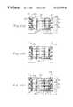
- FIGS. 1 ( a ) through 1 ( d )are cross-sectional views illustrating the respective process steps for fabricating a semiconductor device having a gas-dielectric interconnect structure by using carbon films and SiO 2 films in the first embodiment of the present invention.
- FIG. 2 ( a )is a cross-sectional view of a semiconductor device having a gas-dielectric interconnect structure with an interlayer dielectric film left in the lowermost layer in the second embodiment of the present invention.
- FIG. 2 ( b )is a cross-sectional view of a semiconductor device having a gas-dielectric interconnect structure with encapsulated spaces left in the lowermost layer in the second embodiment of the present invention.
- FIGS. 3 ( a ) through 3 ( d )are cross-sectional views illustrating the respective process steps for fabricating a semiconductor device having a gas-dielectric interconnect structure by using SiO 2 films and SiN films in the third embodiment of the present invention.
- FIGS. 4 ( a ) through 4 ( c )are cross-sectional views illustrating the respective process steps for fabricating a semiconductor device having a gas-dielectric interconnect structure by filling in the gas layers thereof with a low-dielectric-constant film in the fourth embodiment of the present invention.
- FIGS. 5 ( a ) through 5 ( c )are cross-sectional views illustrating the respective process steps for fabricating a semiconductor device having a gas-dielectric interconnect structure by connecting bonding wires thereto and then filling in the gas layers thereof with a low-dielectric-constant film in the fifth embodiment of the present invention.
- FIGS. 6 ( a ) through 6 ( c )are cross-sectional views illustrating the first-half process steps for fabricating a semiconductor device having a gas-dielectric interconnect structure by etching and patterning a metal film until a multilevel interconnect structure is formed in the sixth embodiment of the present invention.
- FIGS. 7 ( a ) and 7 ( b )are cross-sectional views illustrating the second-half process steps for fabricating the semiconductor device having the gas-dielectric interconnect structure by etching and patterning a metal film after the multilevel interconnect structure has been formed in the sixth embodiment.
- FIG. 8is a cross-sectional view illustrating the structure of a semiconductor device in the first variation of the sixth embodiment by using a structure in which an interconnect layer is being formed.
- FIG. 9is a cross-sectional view illustrating the structure of a semiconductor device in the second variation of the sixth embodiment.
- FIGS. 10 ( a ) and 10 ( b )are cross-sectional views illustrating a procedure for forming a gas-dielectric interconnect structure in accordance with a conventional single-damascene process
- FIG. 10 ( c )is a process flow chart thereof.
- FIGS. 11 ( a ) and 11 ( b )are cross-sectional views illustrating a procedure for forming a gas-dielectric interconnect structure in accordance with a conventional dual-damascene process
- FIG. 11 ( c )is a process flow chart thereof.
- FIGS. 12 ( a ) through 12 ( d )are cross-sectional views illustrating the process steps utilizing single damascene technique in the first or third embodiment of the present invention.
- trench isolation regions 2are formed in a P-type silicon substrate 1 .
- MOS transistorseach including source/drain regions 3 , sidewalls 4 , a gate oxide film 5 , a gate electrode 6 and a gate wire 6 a , are formed on the substrate.
- a substrate coating 7made of SiO 2 , is deposited thereon to cover the gate electrodes 6 , the gate wires 6 a , the silicon substrate 1 and the like.
- a lower carbon film 10 a as a provisional film, in which plugs are to be formed, a lower SiO 2 film 9 a , and an upper carbon film 10 b as a provisional film, in which wires are to be formed,are sequentially deposited thereon.
- trenches for wiringare formed in the upper carbon film 10 b by using the lower SiO 2 film 9 a as a stopper.
- contact holes, each extending from the bottom of a trench to reach the source/drain regions 3 through the lower SiO 2 film 9 a and the lower carbon film 10 aare opened.
- the trenches for wiringmay be formed after the contact holes have been formed.
- a barrier metal film and a Cu alloy filmare deposited over the entire surface of the substrate by sputtering and then the Cu alloy film is subjected to a heat treatment at a temperature from 400° C. to 500° C. and made to reflow, thereby filling in the trenches for wiring and contact holes with the Cu alloy.
- a Cu alloy filmmay be formed by a plating technique. Thereafter, the surface of the alloy film is planarized by CMP (chemical mechanical polishing), thereby removing the deposited barrier metal and Cu alloy films except for the portions filled in the trenches for wiring and contact holes.
- portions of the barrier metal film 13 and Cu alloy film 17which are left in the trenches for wiring formed in the upper provisional film 10 b , function as the wires of the first interconnect layer.
- portions of the barrier metal film 13 and Cu alloy film 17which are left in the contact holes formed in the lower provisional film 10 a , function as plugs for vertically connecting the wires in the first interconnect layer to the source/drain regions 3 .
- deposition of the upper SiO 2 film 9 b , lower carbon film 10 a , lower SiO 2 film 9 a and upper carbon film 10 b; formation of the trenches for wiring and contact holes; deposition and reflowing of the barrier metal film 13 and Cu alloy film 17 ; and planarizing by CMPare repeated several times, thereby forming wires and plugs for the second and third interconnect layers.
- an upper SiO 2 film 9 balso functioning as a protective film, is deposited.
- openings 16are formed in the uppermost SiO 2 film 9 b, thereby exposing pad portions of the Cu alloy film 17 functioning as the wires in the third interconnect layer (the uppermost interconnect layer). Also, a dummy opening 30 is formed to pass through multiple carbon films 10 a, 10 b, multiple SiO 2 films 9 a, 9 b and the substrate coating 7 and to reach the gate wire 6 a over the trench isolation region 2 .
- the carbon films 10 a, 10 bare removed by ashing with oxygen (e.g., oxygen plasma).
- oxygene.g., oxygen plasma
- gas layers 40are formed between the wires, each consisting of the barrier metal film 13 and the Cu alloy film 17 .
- a semiconductor device having a so-called “gas-dielectric interconnect structure”can be obtained. That is to say, since the respective wires are insulated from each other via the gas layers 40 , a virtual low-dielectric-constant film having a relative dielectric constant of 1 exists between adjacent wires.
- the dummy opening 30is formed before the carbon films are removed, and the gas layers 40 are formed by performing ashing with oxygen introduced through the dummy opening 30 .
- this structure for a semiconductor devicehas an advantage in that the interconnection strength between the wires and the plugs can be enhanced by increasing the thicknesses of the upper and lower SiO 2 films 9 b, 9 a .
- the gas layers 40 surrounding the wiresare not encapsulated.
- the present inventionis not limited thereto, but is naturally applicable to an embodiment where only the first interconnect layer is provided or an embodiment where only the first and second interconnect layers are provided.
- the present inventionis also applicable to an embodiment where multiple layers including a fourth interconnect layer and so on are further provided in addition to the first to third interconnect layers.
- the lower and upper carbon films 10 a, 10 b, which are removable by ashing with oxygen, and the lower and upper SiO 2 films 9 a, 9 b, which are non-removable by ashingare used for forming the gas layers 40 .
- any method other than ashing with oxygenmay also be used so long as the method enables selective removal.
- films made of a material, which can be selectively etched with respect to the SiO 2 films 9 a, 9 bmay also be used as the provisional films.
- a conductive filmmay also be used as the provisional film.
- insulating films made of a material, which is not removed by the process for removing the carbon films 10 a, 10 bmay also be used.
- a film made of a material having an etching stopper function(e.g., a silicon nitride film) may also be used as the substrate coating 7 .
- the gate wire 6 a and the gate electrode 6are not etched while the dummy opening 30 is being formed.
- the dummy opening 30is preferably formed at a position on a plane where no wires exist as viewed from the above.
- the position, where no wires exist,can be easily located based on designing data.
- the dummy opening 30is formed to reach and pass through the substrate coating 7 .
- the dummy opening 30may be formed so as to reach any carbon film 10 a or 10 b or any SiO 2 film 9 a or 9 b on the way. There are two methods for forming such a dummy opening, as will be described below.
- a silicon dioxide film or the likeis formed instead of the gas layer.
- the gas layeris formed by utilizing the conventional method.
- FIG. 2 ( a )is a cross-sectional view illustrating the structure of a semiconductor device formed in accordance with the first method of this embodiment.
- An interlayer dielectric film 41such as a BPSG film, is formed under the first interconnect layer. Only in the regions above the interlayer dielectric film 41 , the gas layers 40 are formed to surround the wires and plugs.
- the structures of the other parts shown in FIG. 2 ( a )are the same as the counterparts shown in FIG. 1 ( d ).
- Such a structurecan be formed easily by forming the interlayer dielectric film 41 such as a BPSG film instead of the lower carbon film 10 a on the substrate in the step shown in FIG. 1 ( a ), and then performing the same process steps as those illustrated in FIGS. 1 ( a ) through ( d ).
- the interlayer dielectric film 41such as a BPSG film instead of the lower carbon film 10 a
- the portions, where elements such as transistors are formedcan be protected by the interlayer dielectric film 41 with certainty.
- the gas layers 40 to surround the wires and the plugs above the interlayer dielectric film 41an interconnect structure having small parasitic capacitance can be obtained in the same way as in the first embodiment.
- the interlayer dielectric film 41 having a large thicknessis provided as the lowermost layer, it is possible to prevent the gate wire and the gate electrode from being etched during the formation of the dummy opening 30 .
- FIG. 2 ( b )is a cross-sectional view illustrating the structure of a semiconductor device formed in accordance with the second method of this embodiment.
- a gas layer 50 having encapsulated spacesis formed to surround the wires and plugs in the first interconnect layer by utilizing the conventional method without allowing the dummy opening to pass through the layer. Only in the regions above the gas layer 50 , the same gas layers 40 as those of the first embodiment are formed to surround the wires and plugs.
- the structures of the other parts shown in FIG. 2 ( b )are the same as the counterparts shown in FIG. 1 ( d ).
- Such a structurecan be formed easily by forming another SiO 2 film in the state shown in FIG. 1 ( a ), performing ashing with oxygen in such a state and then performing similar process steps as those shown in FIGS. 1 ( a ) through 1 ( d ).
- the dummy opening 30is usually formed to leave the lowermost pair of lower and upper SiO 2 films 9 a, 9 b.
- the upper SiO 2 film 9 b or both of the lower and upper SiO 2 films 9 a, 9 bare opened.
- the dummy opening 30is not formed in the lowermost pair of SiO 2 films 9 a, 9 b, the portions where elements such as transistors are formed can be protected by the gas layer 50 that is substantially shut off from the external world.
- the gas layers 40 communicating with the external worldare formed to surround only the wires over the encapsulated portions.
- an interconnect structure having small parasitic capacitancecan be obtained in the same way as in the first embodiment.
- it is not necessary to form the dummy opening 30 so as to reach the lowermost layerit is possible to prevent with certainty the gate wire and the gate electrode from being etched during the formation of the dummy opening 30 .
- the number of the Sio 2 films 9 a and/or 9 b, through which the dummy opening 30 is not formedis not limited to the ones illustrated in FIG. 2 ( a ) or 2 ( b ).
- two or more interlayer dielectric filmsmay be formed.
- trench isolation regions 2are formed in a P-type silicon substrate 1 .
- MOS transistorseach including source/drain regions 3 , sidewalls 4 , a gate oxide film 5 , a gate electrode 6 and a gate wire 6 a, are formed on the substrate.
- a substrate coating 18made of SiN, is deposited to cover the gate electrodes 6 , the gate wires 6 a, the silicon substrate 1 and the like.
- a lower SiO 2 film 20 a as a provisional film, a lower SiN film 19 a as an insulating film and an upper SiO 2 film 20 bare sequentially deposited thereon.
- trenches for wiringare formed in the upper SiO 2 film 20 b by using the lower SiN film 19 a as a stopper. Thereafter, contact holes, each extending from the bottom of a trench to reach the source/drain regions 3 through the lower SiN film 19 a and the lower SiO 2 film 20 a, are opened. Alternatively, the trenches for wiring may be formed after the contact holes have been formed. Subsequently, a barrier metal film and a Cu alloy film are deposited over the entire surface of the substrate by sputtering and then the Cu alloy film is subjected to a heat treatment at a temperature from 400° C. to 500° C. and made to reflow, thereby filling in the trenches for wiring and contact holes with the Cu alloy.
- the surface of the Cu alloy filmis planarized by CMP, thereby removing the deposited barrier metal and Cu alloy films except for the portions filled in the trenches for wiring and contact holes.
- portions of the barrier metal film 13 and Cu alloy film 17which are left in the trenches for wiring, function as the wires for the first interconnect layer.
- the barrier metal film 13 and Cu alloy film 17which are left in the contact holes, function as plugs for vertically connecting the wires in the first interconnect layer to the source/drain regions 3 .
- deposition of upper SiN film 19 b, lower SiO 2 film 20 a, lower SiN film 19 a and upper SiO, film 20 b; formation of trenches for wiring and contact holes; and deposition and polishing of barrier metal film 13 and Cu alloy film 17are repeated several times, thereby forming wires and plugs for the second and third interconnect layers.
- an upper SiN film 19 balso functioning as a protective film, is deposited.
- openings 16are formed in the uppermost SiN film 19 b, thereby exposing pad portions of the Cu alloy film 17 functioning as the wires of the third interconnect layer (the uppermost interconnect layer).
- a dummy opening 30is formed to pass through multiple lower and upper SiO 2 films 20 a, 20 b, multiple lower and upper SiN films 19 a, 19 b and the substrate coating 18 and to reach the gate wire 6 a over the trench isolation region 2 .
- the position where the dummy opening 30 is formedis determined to reach the gate wire 6 a over the trench isolation region 2 .
- the dummy opening 30is formed over a trench isolation region 2 where no gate wire 6 a exists, then the trench isolation region 2 , made of the same material as that of the respective SiO 2 films 20 a, 20 b, is possibly etched. Thus, it is preferable to form the dummy opening 30 over the gate wire 6 a.
- the lower and upper SiO 2 films 20 a, 20 bare etched with an HF aqueous solution.
- the wires and contact portionsare not etched but left.
- a semiconductor device having a so-called “gas-dielectric interconnect structure”can be obtained. That is to say, since the respective wires are insulated from each other via the gas layers 40 , a virtual low-dielectric-constant film having a relative dielectric constant of 1 exists between adjacent wires.
- a coating insulating film 15made of SiO 2 , for example, is formed over the exposed surfaces of the barrier metal film 13 and gate electrodes 6 by a selective CVD process, for example.
- wet etchingis performed through the dummy opening 30 , and pairs of SiN films and SiO 2 films, which can be mass-produced by a CVD process, are used.
- the lower and upper SiN films 19 a, 19 bcan be thicker, and therefore, the interconnection strength of the wires can be advantageously increased.
- the surfaces of the wires, made of the barrier metal film 13 and the Cu alloy film 17are not exposed but covered with the coating insulating film 15 .
- the relative dielectric constant of the material surrounding the wiresbecomes slightly higher as compared with the semiconductor device having the gas-dielectric interconnect structure of the first embodiment.
- Such a coating insulating film 15may be optionally formed in the first or second embodiment.
- the SiO 2 films 20 a, 20 bwhich can be removed by wet etching with an HF aqueous solution, and the SiN films 19 a, 19 b, which cannot be removed by wet etching, are used in combination.
- any method other than wet etchingmay also be used so long as the method enables selective removal.
- isotropic dry etchingmay be employed if the selectivity thereof is set high.
- films made of a material, which can be selectively etched with respect to the SiN films 19 a, 19 bmay also be used as the provisional films.
- a conductive filmmay also be used as the provisional film.
- insulating films made of a material, which is not removed by the process for removing the Si 0 2 films 20 a, 20 bmay also be used.
- the dummy opening 30is formed to pass through the substrate coating 18 .
- the dummy opening 30may be formed to reach any SiO 2 film 20 a or 20 b or any SiN film 19 a or 19 b on the way, and the gas layers 40 may be formed in the regions between the wires that are located over the selected film. That is to say, a similar structure to that of the second embodiment may be employed.
- FIG. 4 ( a )the same process steps as those illustrated in FIGS. 3 ( a ) through 3 ( d ) of the third embodiment are performed.
- trench isolation regions 2 , and MOS transistorseach including source/drain regions 3 , sidewalls 4 , a gate oxide film 5 , a gate electrode 6 and a gate wire 6 a, have been formed on the substrate.
- a multilevel interconnect structure including wires and plugs, each made of a barrier metal film 13 and a Cu alloy film 17has been formed over the substrate and supported by three lower SiN films 19 a and three upper SiN films 19 b.
- a dummy opening 30has been formed to extend from the uppermost SiN film 19 b, pass through the respective SiN films 19 a, 19 b and the substrate coating 18 and reach the gate wire 6 a.
- Air layers 40have also been formed to surround the wires and plugs. That is to say, a semiconductor device having a gas-dielectric interconnect structure has already been formed at this point in time.
- a low dielectric-constant material having a relative dielectric constant of 2.8 or lessis injected through the dummy opening 30 , thereby filling in the gas layers 40 , which exist in the state shown in FIG. 4 ( a ), with the low-dielectric-constant material.
- a low-dielectric-constant film 22is formed.
- a cytop filmwhich is an organic coating, may be roll-coated and then the coating may be baked if necessary.
- openings 23are formed in the low-dielectric-constant film 22 for exposing the pad portions of the Cu alloy film 17 as the uppermost interconnect layer.
- a low-dielectric-constant materialis filled in between the wires unlike a so-called gas-dielectric interconnect structure.
- the wiresare supported by the low-dielectric-constant film 22 and the strength of the multilevel interconnect structure is increased.
- Cu wiresare formed by filling in the trenches for wiring with a Cu alloy through a heat treatment conducted at a temperature from 400° C. to 450° C., and then the low-dielectric-constant film 22 having a relative dielectric constant of 2.8 or less is filled into the gaps between the Cu wires.
- a semiconductor devicehaving a low-dielectric-constant film that cannot resist to heat of 400° C.
- the relative dielectric constant of the structure of this embodimentis higher than that of a gas dielectric interconnect structure, wiring delay can be reduced with a stable structure. This is because the resistance of the wires and the dielectric constant of the insulating films provided between the wires are further reduced. That is to say, a multilevel interconnect structure having generally optimized properties is realized.
- the low-dielectric-constant film 22is introduced so as to reach the lowermost one of the three interconnect layers.
- the dummy opening 30 for introducing the low-dielectric-constant film 22 therethroughmay be formed to reach an interconnect layer overlying the lowermost layer, and the low-dielectric-constant film 22 may be filled to reach the selected layer.
- the low-dielectric-constant film 22is injected.
- the gas layers 40may be replaced by the low-dielectric-constant film 22 in accordance with a CVD process.
- a fluorine-doped amorphous carbon film ( ⁇ -C:F) having a relative dielectric constant of about 2.4can be formed by performing a plasma CVD process at a temperature of about 350° C. while using C 4 H 8 and CH 4 gases and parallel plate electrode RF plasma.
- trench isolation regions 2 , and MOS transistorseach including source/drain regions 3 , sidewalls 4 , a gate oxide film 5 , a gate electrode 6 and a gate wire 6 a, have been formed on the silicon substrate 1 .
- a dummy opening 30has been formed to extend from the uppermost SiN film 19 b, pass through the respective SiN films 19 a, 19 b and the substrate coating 18 and reach the gate wire 6 a.
- Air layers 40have been formed to surround the wires and the plugs. That is to say, a semiconductor device having a gas-dielectric interconnect structure has already been formed in substantially the same way as the structure shown in FIG. 4 ( a ) of the fourth embodiment. However, this embodiment is different from the fourth embodiment in that openings 16 have been formed in the uppermost SiN film 19 b for exposing the pad portions of the Cu alloy film 17 functioning as the wires in the uppermost layer.
- bonding wires 24are connected to the uppermost Cu alloy film 17 exposed inside the openings 16 .
- a low-dielectric-constant material having a relative dielectric constant of 2.8 or lessis injected through the dummy opening 30 that has been provided to extend from the uppermost to the lowermost interconnect layer.
- the gas layers, which exist in the state shown in FIG. 5 ( a )are filled in with the low-dielectric-constant material, thereby forming a low-dielectric-constant film 22 .
- a cytop filmrelative dielectric constant: 2.1
- the coatingmay be baked if necessary.
- the wiresare also supported by the low-dielectric-constant film 22 .
- a semiconductor deviceattaining the same effects as those of the third embodiment, can also be formed.
- a semiconductor devicehaving a low-dielectric-constant film that cannot resist to heat of 400° C. to 450° C. and the trench-filling Cu wires, can also be formed easily.
- the openings 16 for exposing the pad portions of the uppermost Cu alloy film 17have already been formed in the uppermost SiN film 19 b in the process step shown in FIG. 5 ( a ).
- the low-dielectric-constant film 22is introduced so as to reach the lowermost one of the three interconnect layers.
- the dummy opening 30 for introducing the low-dielectric-constant film 22 therethroughmay be formed to reach an interconnect layer overlying the lowermost layer, and the low-dielectric-constant film 22 may be filled to reach the layer.
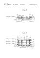
- FIGS. 6 ( a ) through 6 ( c ) and FIGS. 7 ( a ) and 7 ( b )are cross-sectional views illustrating the process steps for fabricating the semiconductor device of this embodiment.
- trench isolation regions 2are formed in a P-type silicon substrate 1 .
- MOS transistorseach including source/drain regions 3 , sidewalls 4 , a gate oxide film 5 , a gate electrode 6 and a gate wire 6 a, are formed on the substrate.
- a substrate coating 7made of SiO 2 , for covering the gate electrodes 6 , the gate wires 6 a, the silicon substrate 1 and the like is formed thereon.
- a carbon film 10 as a provisional film and an SiO 2 film 9are sequentially deposited thereon. Then, contact holes, each reaching the source/drain regions 3 through the SiO 2 film 9 and the carbon film 10 , are opened.
- a barrier metal film and an aluminum (Al) alloy filmare deposited over the entire surface of the substrate by sputtering and patterned.
- the barrier metal film 13 and the Al alloy film 25 on the carbon film 10function as the wires of the first interconnect layer.
- the portions of the barrier metal film 13 and the Al alloy film 25which are left in the contact holes, function as the plugs for vertically connecting the wires in the first interconnect layer to the source/drain regions 3 .
- an SiO 2 film 26is deposited over the entire surface of the substrate.
- the SiO 2 film 26is formed to cover the upper and side surfaces of the carbon film 10 and the Al alloy film 25 .
- a carbon film 10is further deposited thereon.
- through holes 27are formed to pass through the carbon film 10 and the SiO 2 film 26 and reach the Al alloy film 25 .
- barrier metal films 13 and Al alloy films 25 and deposition of carbon films 10 and SiO 2 films 26are repeated several times, thereby forming wires and plugs for the second and third interconnect layers.
- an SiO 2 film 26also functioning as a protective film, is deposited.
- openings 16are formed through the uppermost SiO 2 film 26 , thereby exposing pad portions of the Al alloy film 25 functioning as the wires of the third interconnect layer (the uppermost interconnect layer). Also, a dummy opening 30 is formed to pass through multiple carbon films 10 , multiple SiO 2 films 26 and the substrate coating 7 and to reach the gate wire 6 a over the trench isolation region 2 .
- the carbon films 10are removed by ashing with oxygen.
- gas layers 40are formed between the wires, each made of the barrier metal film 13 and the Al alloy film 25 .
- a semiconductor device having a so-called “gas-dielectric interconnect structure”can be obtained. That is to say, since the respective wires are insulated from each other via the gas layers 40 , a virtual low-dielectric-constant film having a relative dielectric constant of 1 exists between adjacent wires.
- this embodimentcan utilize a generally employed process for forming an interconnect layer by etching and patterning a metal film. Moreover, since the contact area between the Al alloy film 25 and the SiO 2 film 26 is large, the function of the SiO 2 film 26 interconnecting the Al alloy film 25 can be enhanced.
- the principal portion of the wires and plugsis made of the same metal material, i.e., an aluminum alloy.
- the wires and plugsmay be made of different materials, for example, an aluminum alloy and tungsten, respectively.
- the method of this embodimentmay also employ the structure of the second embodiment shown in FIGS. 2 ( a ) and 2 ( b ) where the lowermost layer is filled with the interlayer dielectric film 41 or has the encapsulated gas layers 50 left.
- the method of this embodimentmay use SiO 2 films as films to be removed and SiN films as insulating film to be left as in the third embodiment.
- the method of this embodimentmay replace the gas layers 40 with the low-dielectric-constant film 22 as in the fourth embodiment.
- a planar insulating filmmay be formed so as to come into contact with the lower surface of the metal film and interconnect the metal film.
- Such an insulating filmmay be formed by the methods of the following modified embodiments.
- FIG. 8is a cross-sectional view illustrating a part of the process (a process step corresponding to that shown in FIG. 7 ( a )) for fabricating a semiconductor device in the first variation of the sixth embodiment.
- a planar SiO 2 film 9is formed on the carbon film 10 and then formation of contact holes and deposition of the barrier metal film and the Al alloy film may be performed.
- the SiO 2 film 26is deposited over the substrate.
- the Al alloy film 25is interconnected so as to be wrapped by the SiO 2 films 9 and 26 in all the directions.
- the Al alloy film 25can be interconnected very strongly by the SiO 2 films 9 and 26 .
- FIG. 9is a cross-sectional view illustrating a structure for a semiconductor device in the second variation of the sixth embodiment.
- a planar SiO 2 film 9is provided on the carbon film 10 , but the SiO 2 film 26 such as that shown in FIG. 8 is not provided.
- This structurecan be formed by performing the steps of: forming the planar SiO 2 film 9 on the carbon film 10 ; forming the contact holes; and depositing and patterning the barrier metal film and the Al alloy film.
- the SiO 2 film 26is not deposited on the Al alloy film 25 .
- an SiO 2 film 29is deposited as a protective film over only the Al alloy film 25 in the uppermost interconnect layer.
- the structure shown in FIG. 9can also interconnect the Al alloy film 25 strongly with the SiO 2 film 9 if the thickness of the SiO 2 film 9 is set at a sufficiently large value.
- a pair of single layerse.g., carbon film and SiO 2 film or SiO 2 film and SiN film, is used as a combination of provisional film and insulating film.
- At least one of the pair of filmsmay be a multilayer film.
- Various passive elementssuch as resistors and capacitors, diodes and the like may be formed on the silicon substrate 1 .
- MOS transistorseach including a trench isolation region 2 , source/drain regions 3 , sidewalls 4 , a gate oxide film 5 , a gate electrode 6 and a gate wire 6 a, are formed on the silicon substrate 1 .
- Other types of transistorssuch as bipolar transistors may be formed instead of or in addition to the MOS transistors.
- the substrate coating 7 or 18made of SiO 2 or SiN, is provided.
- the substrate coating 7 or 18may be omitted so long as the carbon films 10 a, 10 b or the SiO 2 films 20 a, 20 b can be removed without doing any damage on the silicon substrate I and the gate electrodes 6 .
- a Cu alloyis used as a material for the wires.
- any conductive material other than Cue.g., a metal such as Al or an alloy thereof, may also be used.
- the barrier metal film 13may be omitted.
- trenches for wiring and holesare formed and then wires and plugs are simultaneously formed in accordance with a so-called “dual-damascene process”.
- a so-called “single-damascene process”, in which formation of holes and plugs and formation of trenches for wiring and wires are performed separately,may be naturally employed.
- FIGS. 12 ( a ) through 12 ( d )are cross-sectional views illustrating the process steps for forming interconnect layers by utilizing the single damascene technique.
- a lower provisional filmis deposited on a substrate, a hole is formed in the lower provisional film, and then the hole is filled in with a conductive material, thereby forming a plug.
- the substratemay be either a semiconductor substrate or a structure in which an interconnect layer has already been formed on a semiconductor substrate.
- the lower provisional filmis a member corresponding to the lower carbon film 10 a of the first embodiment or the lower SiO 2 film 20 a of the third embodiment.
- a lower insulating film and an upper provisional filmare deposited on the substrate.
- the lower insulating filmis a member corresponding to the lower SiO 2 film 9 a of the first embodiment to the lower SiN film 19 a of the third embodiment.
- the upper provisional filmis a member corresponding to the upper carbon film 10 b of the first embodiment or the upper SiO 2 film 20 b of the third embodiment.
- a trench for wireis formed in the upper provisional film, and the trench for wire is filled in with a conductive material, thereby forming a wire.
- an upper insulating film and a lower provisional filmare sequentially stacked on the substrate.
- the upper insulating filmis a member corresponding to the upper SiO 2 film 9 b of the first embodiment or the upper SiN film 19 b of the third embodiment.
- the subsequent process stepsare the same as the counterparts of the above-described first and third embodiments, and therefore, the description and illustration thereof will be omitted herein.
- a plug for the next interconnect layeris formed in the uppermost lower provisional film shown in FIG. 12 ( d ).
- a gas-dielectric interconnect structureattaining the same effects as those of the first and third embodiments, can also be formed in accordance with the single damascene process shown in FIGS. 12 ( a ) through 12 ( d ).
- This single damascene processis particularly effective to a semiconductor device with an even higher density, in which a hole has an even higher aspect ratio.
Landscapes
- Engineering & Computer Science (AREA)
- Physics & Mathematics (AREA)
- Condensed Matter Physics & Semiconductors (AREA)
- General Physics & Mathematics (AREA)
- Computer Hardware Design (AREA)
- Microelectronics & Electronic Packaging (AREA)
- Power Engineering (AREA)
- Manufacturing & Machinery (AREA)
- Internal Circuitry In Semiconductor Integrated Circuit Devices (AREA)
Abstract
Description
Claims (12)
Priority Applications (1)
| Application Number | Priority Date | Filing Date | Title |
|---|---|---|---|
| US09/986,289US6534868B2 (en) | 1997-08-21 | 2001-11-08 | Semiconductor device and method for fabricating the same |
Applications Claiming Priority (2)
| Application Number | Priority Date | Filing Date | Title |
|---|---|---|---|
| JP9-224987 | 1997-08-21 | ||
| JP22498797 | 1997-08-21 |
Related Child Applications (1)
| Application Number | Title | Priority Date | Filing Date |
|---|---|---|---|
| US09/986,289DivisionUS6534868B2 (en) | 1997-08-21 | 2001-11-08 | Semiconductor device and method for fabricating the same |
Publications (1)
| Publication Number | Publication Date |
|---|---|
| US6333255B1true US6333255B1 (en) | 2001-12-25 |
Family
ID=16822331
Family Applications (2)
| Application Number | Title | Priority Date | Filing Date |
|---|---|---|---|
| US09/137,150Expired - LifetimeUS6333255B1 (en) | 1997-08-21 | 1998-08-20 | Method for making semiconductor device containing low carbon film for interconnect structures |
| US09/986,289Expired - LifetimeUS6534868B2 (en) | 1997-08-21 | 2001-11-08 | Semiconductor device and method for fabricating the same |
Family Applications After (1)
| Application Number | Title | Priority Date | Filing Date |
|---|---|---|---|
| US09/986,289Expired - LifetimeUS6534868B2 (en) | 1997-08-21 | 2001-11-08 | Semiconductor device and method for fabricating the same |
Country Status (1)
| Country | Link |
|---|---|
| US (2) | US6333255B1 (en) |
Cited By (63)
| Publication number | Priority date | Publication date | Assignee | Title |
|---|---|---|---|---|
| US20020001778A1 (en)* | 2000-06-08 | 2002-01-03 | Applied Materials, Inc. | Photolithography scheme using a silicon containing resist |
| US6441491B1 (en)* | 2000-10-25 | 2002-08-27 | International Business Machines Corporation | Ultralow dielectric constant material as an intralevel or interlevel dielectric in a semiconductor device and electronic device containing the same |
| US6551915B2 (en)* | 2001-07-03 | 2003-04-22 | Taiwan Semiconductor Manufacturing Co., Ltd. | Thermal annealing/hydrogen containing plasma method for forming structurally stable low contact resistance damascene conductor structure |
| US6559548B1 (en)* | 1999-03-19 | 2003-05-06 | Kabushiki Kaisha Toshiba | Wiring structure of semiconductor device |
| US20030091938A1 (en)* | 2000-02-17 | 2003-05-15 | Applied Materials, Inc. | Method of depositing an amorphous carbon layer |
| US6577011B1 (en)* | 1997-07-10 | 2003-06-10 | International Business Machines Corporation | Chip interconnect wiring structure with low dielectric constant insulator and methods for fabricating the same |
| US6614096B2 (en)* | 2001-06-29 | 2003-09-02 | Kabushiki Kaisha Toshiba | Method for manufacturing a semiconductor device and a semiconductor device |
| US20030170974A1 (en)* | 2002-03-07 | 2003-09-11 | Toyokazu Sakata | Method of fabricating a semiconductor device |
| US20030186535A1 (en)* | 2002-03-26 | 2003-10-02 | Lawrence D. Wong | Method of making semiconductor device using a novel interconnect cladding layer |
| US6661094B2 (en)* | 2001-03-27 | 2003-12-09 | Intel Corporation | Semiconductor device having a dual damascene interconnect spaced from a support structure |
| US20040056356A1 (en)* | 2000-01-19 | 2004-03-25 | Macneil John | Methods and apparatus for forming a film on a substrate |
| US6737725B2 (en)* | 2000-08-31 | 2004-05-18 | International Business Machines Corporation | Multilevel interconnect structure containing air gaps and method for making |
| US6747307B1 (en)* | 2000-04-04 | 2004-06-08 | Koninklijke Philips Electronics N.V. | Combined transistor-capacitor structure in deep sub-micron CMOS for power amplifiers |
| US6768200B2 (en) | 2000-10-25 | 2004-07-27 | International Business Machines Corporation | Ultralow dielectric constant material as an intralevel or interlevel dielectric in a semiconductor device |
| US6774005B2 (en)* | 2001-07-26 | 2004-08-10 | Infineon Technologies Ag | Method for fabricating a metal carbide layer and method for fabricating a trench capacitor containing a metal carbide |
| US6780753B2 (en) | 2002-05-31 | 2004-08-24 | Applied Materials Inc. | Airgap for semiconductor devices |
| US20040259355A1 (en)* | 2003-06-17 | 2004-12-23 | Zhiping Yin | Boron-doped amorphous carbon film for use as a hard etch mask during the formation of a semiconductor device |
| US20050023697A1 (en)* | 2000-01-18 | 2005-02-03 | Micron Technology, Inc. | Methods for making integrated-circuit wiring from copper, silver, gold, and other metals |
| US6852647B2 (en) | 2002-03-29 | 2005-02-08 | Applied Materials, Inc. | Removable amorphous carbon CMP stop |
| US6855627B1 (en)* | 2002-12-04 | 2005-02-15 | Advanced Micro Devices, Inc. | Method of using amorphous carbon to prevent resist poisoning |
| US20050042879A1 (en)* | 2003-08-22 | 2005-02-24 | Zhiping Yin | Masking methods |
| US20050064718A1 (en)* | 2003-09-24 | 2005-03-24 | Zhiping Yin | Antireflective coating for use during the manufacture of a semiconductor device |
| US20050093052A1 (en)* | 1999-08-31 | 2005-05-05 | Agarwal Vishnu K. | Structurally-stabilized capacitors and method of making of same |
| US20050199013A1 (en)* | 2004-03-12 | 2005-09-15 | Applied Materials, Inc. | Use of amorphous carbon film as a hardmask in the fabrication of optical waveguides |
| US20050199585A1 (en)* | 2004-03-12 | 2005-09-15 | Applied Materials, Inc. | Method of depositing an amorphous carbon film for metal etch hardmask application |
| US20050202683A1 (en)* | 2004-03-12 | 2005-09-15 | Applied Materials, Inc. | Method of depositing an amorphous carbon film for etch hardmask application |
| US6949472B1 (en)* | 2004-05-03 | 2005-09-27 | Taiwan Semiconductor Manufacturing Co., Ltd | Method for high kinetic energy plasma barrier deposition |
| US20050287771A1 (en)* | 2004-03-05 | 2005-12-29 | Applied Materials, Inc. | Liquid precursors for the CVD deposition of amorphous carbon films |
| US6984892B2 (en)* | 2001-03-28 | 2006-01-10 | Lam Research Corporation | Semiconductor structure implementing low-K dielectric materials and supporting stubs |
| US20060006538A1 (en)* | 2004-07-02 | 2006-01-12 | Lsi Logic Corporation | Extreme low-K interconnect structure and method |
| US7023059B1 (en)* | 2004-03-01 | 2006-04-04 | Advanced Micro Devices, Inc. | Trenches to reduce lateral silicide growth in integrated circuit technology |
| US20060086954A1 (en)* | 2000-12-27 | 2006-04-27 | Natarajan Sanjay S | Multi-layer film stack for extinction of substrate reflections during patterning |
| US20060099131A1 (en)* | 2004-11-03 | 2006-05-11 | Kellogg Brown And Root, Inc. | Maximum reaction rate converter system for exothermic reactions |
| US20060202302A1 (en)* | 2003-09-30 | 2006-09-14 | International Business Machines Corporation | Adjustable self-aligned air gap dielectric for low capacitance wiring |
| US7115524B2 (en) | 2004-05-17 | 2006-10-03 | Micron Technology, Inc. | Methods of processing a semiconductor substrate |
| US20070007635A1 (en)* | 2005-07-07 | 2007-01-11 | Micron Technology, Inc. | Self aligned metal gates on high-k dielectrics |
| US20070045752A1 (en)* | 2005-08-31 | 2007-03-01 | Leonard Forbes | Self aligned metal gates on high-K dielectrics |
| US7262505B2 (en) | 2000-01-18 | 2007-08-28 | Micron Technology, Inc. | Selective electroless-plated copper metallization |
| US7301190B2 (en) | 2000-01-18 | 2007-11-27 | Micron Technology, Inc. | Structures and methods to enhance copper metallization |
| CN100353542C (en)* | 2003-06-11 | 2007-12-05 | 台湾积体电路制造股份有限公司 | Integrated circuit and its forming method and electronic component |
| US20070286954A1 (en)* | 2006-06-13 | 2007-12-13 | Applied Materials, Inc. | Methods for low temperature deposition of an amorphous carbon layer |
| US7319065B1 (en)* | 2003-08-08 | 2008-01-15 | Advanced Micro Devices, Inc. | Semiconductor component and method of manufacture |
| US20080038518A1 (en)* | 2002-09-13 | 2008-02-14 | Shipley Company, L.L.C. | Air gap formation |
| US7354631B2 (en) | 2003-11-06 | 2008-04-08 | Micron Technology, Inc. | Chemical vapor deposition apparatus and methods |
| US7394157B2 (en) | 2000-01-18 | 2008-07-01 | Micron Technology, Inc. | Integrated circuit and seed layers |
| US20080166874A1 (en)* | 2007-01-05 | 2008-07-10 | International Business Machines Corporation | Formation of vertical devices by electroplating |
| US20080179750A1 (en)* | 2007-01-11 | 2008-07-31 | Stmicroelectronics Sa | Interconnections of an integrated electronic circuit |
| US20080237646A1 (en)* | 2000-10-17 | 2008-10-02 | Matsushita Electric Industrial Co., Ltd. | Semiconductor integrated circuit device and method of producing the same |
| US20080245559A1 (en)* | 2006-05-31 | 2008-10-09 | Georgia Tech Research Corporation | Variable interconnect geometry for electronic packages and fabrication methods |
| US20090093128A1 (en)* | 2007-10-08 | 2009-04-09 | Martin Jay Seamons | Methods for high temperature deposition of an amorphous carbon layer |
| US20090269923A1 (en)* | 2008-04-25 | 2009-10-29 | Lee Sang M | Adhesion and electromigration improvement between dielectric and conductive layers |
| US7660644B2 (en) | 2001-07-27 | 2010-02-09 | Applied Materials, Inc. | Atomic layer deposition apparatus |
| US7670469B2 (en) | 2000-01-18 | 2010-03-02 | Micron Technology, Inc. | Methods and apparatus for making integrated-circuit wiring from copper, silver, gold, and other metals |
| US7709402B2 (en) | 2006-02-16 | 2010-05-04 | Micron Technology, Inc. | Conductive layers for hafnium silicon oxynitride films |
| CN102054818B (en)* | 2009-11-10 | 2012-08-22 | 中芯国际集成电路制造(上海)有限公司 | Interconnection structure and manufacture method thereof |
| TWI550869B (en)* | 2012-08-23 | 2016-09-21 | Semiconductor Mfg Int Shanghai | Semiconductor element structure and manufacturing method thereof |
| US9653327B2 (en) | 2011-05-12 | 2017-05-16 | Applied Materials, Inc. | Methods of removing a material layer from a substrate using water vapor treatment |
| US9991399B2 (en) | 2012-10-04 | 2018-06-05 | Cree, Inc. | Passivation structure for semiconductor devices |
| US10062666B2 (en) | 2015-10-30 | 2018-08-28 | Advanced Research Corporation | Catch flexure systems, devices and methods |
| US11031338B2 (en) | 2018-12-24 | 2021-06-08 | Samsung Electronics Co., Ltd. | Semiconductor device and method for fabricating the same |
| US20220359707A1 (en)* | 2019-06-14 | 2022-11-10 | Taiwan Semiconductor Manufacturing Company Limited | Semiconductor arrangement with airgap and method of forming |
| US20240194525A1 (en)* | 2017-08-31 | 2024-06-13 | Taiwan Semiconductor Manufacturing Co., Ltd. | Vias for Cobalt-Based Interconnects and Methods of Fabrication Thereof |
| US12444649B2 (en)* | 2024-02-19 | 2025-10-14 | Parabellum Strategic Opportunties Fund LLC | Vias for cobalt-based interconnects and methods of fabrication thereof |
Families Citing this family (16)
| Publication number | Priority date | Publication date | Assignee | Title |
|---|---|---|---|---|
| JP2003142226A (en)* | 2001-10-31 | 2003-05-16 | Ngk Spark Plug Co Ltd | Spark plug |
| EP1521301A1 (en)* | 2003-09-30 | 2005-04-06 | Interuniversitaire Microelectronica Centrum vzw ( IMEC) | Method of formation of airgaps around interconnecting line |
| US6875685B1 (en) | 2003-10-24 | 2005-04-05 | International Business Machines Corporation | Method of forming gas dielectric with support structure |
| US7737020B1 (en)* | 2005-12-21 | 2010-06-15 | Xilinx, Inc. | Method of fabricating CMOS devices using fluid-based dielectric materials |
| FR2897198B1 (en)* | 2006-02-08 | 2008-09-19 | Commissariat Energie Atomique | INTERCONNECTION STRUCTURE AND METHOD OF MAKING |
| US7510323B2 (en)* | 2006-03-14 | 2009-03-31 | International Business Machines Corporation | Multi-layered thermal sensor for integrated circuits and other layered structures |
| US7518481B2 (en)* | 2006-06-30 | 2009-04-14 | Intel Corporation | Slotted magnetic material for integrated circuit inductors |
| JP2008166422A (en)* | 2006-12-27 | 2008-07-17 | Toshiba Corp | Semiconductor device |
| JP2008205283A (en)* | 2007-02-21 | 2008-09-04 | Matsushita Electric Ind Co Ltd | Wiring structure of semiconductor integrated circuit device, design method and design apparatus thereof |
| US7858513B2 (en)* | 2007-06-18 | 2010-12-28 | Organicid, Inc. | Fabrication of self-aligned via holes in polymer thin films |
| US7936072B2 (en)* | 2007-11-12 | 2011-05-03 | Renesas Electronics Corporation | Semiconductor device having dual damascene structure |
| KR20100107661A (en)* | 2009-03-26 | 2010-10-06 | 삼성전자주식회사 | Method of fabricating nonvolatile memory device having vertical structure |
| US8384214B2 (en)* | 2009-10-13 | 2013-02-26 | United Microelectronics Corp. | Semiconductor structure, pad structure and protection structure |
| JP2014209522A (en) | 2013-04-16 | 2014-11-06 | 富士通株式会社 | Semiconductor device and manufacturing method of the same |
| KR102678907B1 (en) | 2016-12-20 | 2024-06-26 | 삼성전자주식회사 | Nonvolatile memory device |
| US12341058B2 (en)* | 2022-02-04 | 2025-06-24 | Globalfoundries Singapore Pte. Ltd. | Air gap through at least two metal layers |
Citations (19)
| Publication number | Priority date | Publication date | Assignee | Title |
|---|---|---|---|---|
| JPS61107747A (en) | 1984-10-31 | 1986-05-26 | Toshiba Corp | Manufacturing method of semiconductor device |
| JPS61107746A (en) | 1984-10-31 | 1986-05-26 | Fujitsu Ltd | Manufacturing method of semiconductor device |
| US4933743A (en) | 1989-03-11 | 1990-06-12 | Fairchild Semiconductor Corporation | High performance interconnect system for an integrated circuit |
| US5117276A (en) | 1989-08-14 | 1992-05-26 | Fairchild Camera And Instrument Corp. | High performance interconnect system for an integrated circuit |
| JPH0685070A (en) | 1992-09-07 | 1994-03-25 | Mitsubishi Electric Corp | Formation of multilayer interconnection |
| US5324683A (en) | 1993-06-02 | 1994-06-28 | Motorola, Inc. | Method of forming a semiconductor structure having an air region |
| US5468685A (en) | 1992-03-31 | 1995-11-21 | Mitsubishi Denki Kabushiki Kaisha | Method for producing a semiconductor integrated circuit |
| JPH0817918A (en) | 1994-06-29 | 1996-01-19 | Toshiba Corp | Semiconductor device and manufacturing method thereof |
| US5530290A (en) | 1992-12-15 | 1996-06-25 | International Business Machines Corporation | Large scale IC personalization method employing air dielectric structure for extended conductor |
| US5559055A (en) | 1994-12-21 | 1996-09-24 | Advanced Micro Devices, Inc. | Method of decreased interlayer dielectric constant in a multilayer interconnect structure to increase device speed performance |
| JPH08250592A (en) | 1994-09-30 | 1996-09-27 | Hewlett Packard Co <Hp> | Air - dielectric transmission line for integrated circuit |
| JPH09172068A (en) | 1995-12-18 | 1997-06-30 | Nec Corp | Method for manufacturing semiconductor device |
| JPH10199978A (en) | 1997-01-14 | 1998-07-31 | Sony Corp | Semiconductor device and its manufacture |
| US5798559A (en) | 1996-03-29 | 1998-08-25 | Vlsi Technology, Inc. | Integrated circuit structure having an air dielectric and dielectric support pillars |
| JPH10294316A (en) | 1997-04-18 | 1998-11-04 | Nec Corp | Semiconductor device and manufacture thereof |
| US5900668A (en) | 1995-11-30 | 1999-05-04 | Advanced Micro Devices, Inc. | Low capacitance interconnection |
| US5923074A (en) | 1996-12-03 | 1999-07-13 | Texas Instruments Incorporated | Low capacitance interconnect structure for integrated circuits using decomposed polymers |
| US5950102A (en) | 1997-02-03 | 1999-09-07 | Industrial Technology Research Institute | Method for fabricating air-insulated multilevel metal interconnections for integrated circuits |
| US5994776A (en) | 1996-01-11 | 1999-11-30 | Advanced Micro Devices, Inc. | Interlevel dielectric with multiple air gaps between conductive lines of an integrated circuit |
Family Cites Families (2)
| Publication number | Priority date | Publication date | Assignee | Title |
|---|---|---|---|---|
| US5164699A (en)* | 1990-12-17 | 1992-11-17 | Hughes Aircraft Company | Via resistors within-multi-layer, 3 dimensional structures substrates |
| US5485038A (en)* | 1993-07-15 | 1996-01-16 | Hughes Aircraft Company | Microelectronic circuit substrate structure including photoimageable epoxy dielectric layers |
- 1998
- 1998-08-20USUS09/137,150patent/US6333255B1/ennot_activeExpired - Lifetime
- 2001
- 2001-11-08USUS09/986,289patent/US6534868B2/ennot_activeExpired - Lifetime
Patent Citations (21)
| Publication number | Priority date | Publication date | Assignee | Title |
|---|---|---|---|---|
| JPS61107747A (en) | 1984-10-31 | 1986-05-26 | Toshiba Corp | Manufacturing method of semiconductor device |
| JPS61107746A (en) | 1984-10-31 | 1986-05-26 | Fujitsu Ltd | Manufacturing method of semiconductor device |
| US4933743A (en) | 1989-03-11 | 1990-06-12 | Fairchild Semiconductor Corporation | High performance interconnect system for an integrated circuit |
| US5117276A (en) | 1989-08-14 | 1992-05-26 | Fairchild Camera And Instrument Corp. | High performance interconnect system for an integrated circuit |
| US5468685A (en) | 1992-03-31 | 1995-11-21 | Mitsubishi Denki Kabushiki Kaisha | Method for producing a semiconductor integrated circuit |
| JPH0685070A (en) | 1992-09-07 | 1994-03-25 | Mitsubishi Electric Corp | Formation of multilayer interconnection |
| US5530290A (en) | 1992-12-15 | 1996-06-25 | International Business Machines Corporation | Large scale IC personalization method employing air dielectric structure for extended conductor |
| US5324683A (en) | 1993-06-02 | 1994-06-28 | Motorola, Inc. | Method of forming a semiconductor structure having an air region |
| JPH0817918A (en) | 1994-06-29 | 1996-01-19 | Toshiba Corp | Semiconductor device and manufacturing method thereof |
| JPH08250592A (en) | 1994-09-30 | 1996-09-27 | Hewlett Packard Co <Hp> | Air - dielectric transmission line for integrated circuit |
| US5567982A (en) | 1994-09-30 | 1996-10-22 | Bartelink; Dirk J. | Air-dielectric transmission lines for integrated circuits |
| US5559055A (en) | 1994-12-21 | 1996-09-24 | Advanced Micro Devices, Inc. | Method of decreased interlayer dielectric constant in a multilayer interconnect structure to increase device speed performance |
| US5900668A (en) | 1995-11-30 | 1999-05-04 | Advanced Micro Devices, Inc. | Low capacitance interconnection |
| JPH09172068A (en) | 1995-12-18 | 1997-06-30 | Nec Corp | Method for manufacturing semiconductor device |
| US5994776A (en) | 1996-01-11 | 1999-11-30 | Advanced Micro Devices, Inc. | Interlevel dielectric with multiple air gaps between conductive lines of an integrated circuit |
| US5798559A (en) | 1996-03-29 | 1998-08-25 | Vlsi Technology, Inc. | Integrated circuit structure having an air dielectric and dielectric support pillars |
| US5923074A (en) | 1996-12-03 | 1999-07-13 | Texas Instruments Incorporated | Low capacitance interconnect structure for integrated circuits using decomposed polymers |
| JPH10199978A (en) | 1997-01-14 | 1998-07-31 | Sony Corp | Semiconductor device and its manufacture |
| US5950102A (en) | 1997-02-03 | 1999-09-07 | Industrial Technology Research Institute | Method for fabricating air-insulated multilevel metal interconnections for integrated circuits |
| JPH10294316A (en) | 1997-04-18 | 1998-11-04 | Nec Corp | Semiconductor device and manufacture thereof |
| US6064118A (en) | 1997-04-18 | 2000-05-16 | Nec Corporation | Multilevel interconnection structure having an air gap between interconnects |
Non-Patent Citations (3)
| Title |
|---|
| M.B. Anand,e t al., "NURA: A Feasible, Gas-Dielectric Interconnect Process", 1996 IEEE Symposium on VLSI Technology Digest of Technical Papers, pp. 82-83, 1996. |
| T. Hasegawa et al., "Possibility of Organic Film for 0.13 mum Rule Time", Semiconductor World, pp. 89-93, Feb., 1996. |
| T. Hasegawa et al., "Possibility of Organic Film for 0.13 μm Rule Time", Semiconductor World, pp. 89-93, Feb., 1996. |
Cited By (118)
| Publication number | Priority date | Publication date | Assignee | Title |
|---|---|---|---|---|
| US6577011B1 (en)* | 1997-07-10 | 2003-06-10 | International Business Machines Corporation | Chip interconnect wiring structure with low dielectric constant insulator and methods for fabricating the same |
| US6864583B2 (en)* | 1999-03-19 | 2005-03-08 | Kabushiki Kaisha Toshiba | Wiring structure of semiconductor device |
| US6559548B1 (en)* | 1999-03-19 | 2003-05-06 | Kabushiki Kaisha Toshiba | Wiring structure of semiconductor device |
| US20030205814A1 (en)* | 1999-03-19 | 2003-11-06 | Kabushiki Kaisha Toshiba | Wiring structure of semiconductor device |
| US20050093052A1 (en)* | 1999-08-31 | 2005-05-05 | Agarwal Vishnu K. | Structurally-stabilized capacitors and method of making of same |
| US7488665B2 (en)* | 1999-08-31 | 2009-02-10 | Micron Technology, Inc. | Structurally-stabilized capacitors and method of making of same |
| US20050023697A1 (en)* | 2000-01-18 | 2005-02-03 | Micron Technology, Inc. | Methods for making integrated-circuit wiring from copper, silver, gold, and other metals |
| US7535103B2 (en) | 2000-01-18 | 2009-05-19 | Micron Technology, Inc. | Structures and methods to enhance copper metallization |
| US7670469B2 (en) | 2000-01-18 | 2010-03-02 | Micron Technology, Inc. | Methods and apparatus for making integrated-circuit wiring from copper, silver, gold, and other metals |
| US7262505B2 (en) | 2000-01-18 | 2007-08-28 | Micron Technology, Inc. | Selective electroless-plated copper metallization |
| US8779596B2 (en) | 2000-01-18 | 2014-07-15 | Micron Technology, Inc. | Structures and methods to enhance copper metallization |
| US7368378B2 (en) | 2000-01-18 | 2008-05-06 | Micron Technology, Inc. | Methods for making integrated-circuit wiring from copper, silver, gold, and other metals |
| US7301190B2 (en) | 2000-01-18 | 2007-11-27 | Micron Technology, Inc. | Structures and methods to enhance copper metallization |
| US7745934B2 (en) | 2000-01-18 | 2010-06-29 | Micron Technology, Inc. | Integrated circuit and seed layers |
| US7262130B1 (en) | 2000-01-18 | 2007-08-28 | Micron Technology, Inc. | Methods for making integrated-circuit wiring from copper, silver, gold, and other metals |
| US7378737B2 (en) | 2000-01-18 | 2008-05-27 | Micron Technology, Inc. | Structures and methods to enhance copper metallization |
| US7394157B2 (en) | 2000-01-18 | 2008-07-01 | Micron Technology, Inc. | Integrated circuit and seed layers |
| US7402516B2 (en) | 2000-01-18 | 2008-07-22 | Micron Technology, Inc. | Method for making integrated circuits |
| US7253521B2 (en)* | 2000-01-18 | 2007-08-07 | Micron Technology, Inc. | Methods for making integrated-circuit wiring from copper, silver, gold, and other metals |
| US20040056356A1 (en)* | 2000-01-19 | 2004-03-25 | Macneil John | Methods and apparatus for forming a film on a substrate |
| US6841341B2 (en) | 2000-02-17 | 2005-01-11 | Applied Materials, Inc. | Method of depositing an amorphous carbon layer |
| US20030091938A1 (en)* | 2000-02-17 | 2003-05-15 | Applied Materials, Inc. | Method of depositing an amorphous carbon layer |
| US7335462B2 (en) | 2000-02-17 | 2008-02-26 | Applied Materials, Inc. | Method of depositing an amorphous carbon layer |
| US7223526B2 (en) | 2000-02-17 | 2007-05-29 | Applied Materials, Inc. | Method of depositing an amorphous carbon layer |
| US20050233257A1 (en)* | 2000-02-17 | 2005-10-20 | Applied Materials, Inc. | Photolithography scheme using a silicon containing resist |
| US7332262B2 (en) | 2000-02-17 | 2008-02-19 | Applied Materials, Inc. | Photolithography scheme using a silicon containing resist |
| US6747307B1 (en)* | 2000-04-04 | 2004-06-08 | Koninklijke Philips Electronics N.V. | Combined transistor-capacitor structure in deep sub-micron CMOS for power amplifiers |
| US20020001778A1 (en)* | 2000-06-08 | 2002-01-03 | Applied Materials, Inc. | Photolithography scheme using a silicon containing resist |
| US6967072B2 (en) | 2000-06-08 | 2005-11-22 | Applied Materials, Inc. | Photolithography scheme using a silicon containing resist |
| US6737725B2 (en)* | 2000-08-31 | 2004-05-18 | International Business Machines Corporation | Multilevel interconnect structure containing air gaps and method for making |
| US20080237646A1 (en)* | 2000-10-17 | 2008-10-02 | Matsushita Electric Industrial Co., Ltd. | Semiconductor integrated circuit device and method of producing the same |
| US6768200B2 (en) | 2000-10-25 | 2004-07-27 | International Business Machines Corporation | Ultralow dielectric constant material as an intralevel or interlevel dielectric in a semiconductor device |
| US6441491B1 (en)* | 2000-10-25 | 2002-08-27 | International Business Machines Corporation | Ultralow dielectric constant material as an intralevel or interlevel dielectric in a semiconductor device and electronic device containing the same |
| US6541398B2 (en) | 2000-10-25 | 2003-04-01 | International Business Machines Corporation | Ultralow dielectric constant material as an intralevel or interlevel dielectric in a semiconductor device and electronic device containing the same |
| US20060086954A1 (en)* | 2000-12-27 | 2006-04-27 | Natarajan Sanjay S | Multi-layer film stack for extinction of substrate reflections during patterning |
| US6661094B2 (en)* | 2001-03-27 | 2003-12-09 | Intel Corporation | Semiconductor device having a dual damascene interconnect spaced from a support structure |
| US6984892B2 (en)* | 2001-03-28 | 2006-01-10 | Lam Research Corporation | Semiconductor structure implementing low-K dielectric materials and supporting stubs |
| US7425501B2 (en)* | 2001-03-28 | 2008-09-16 | Lam Research Corporation | Semiconductor structure implementing sacrificial material and methods for making and implementing the same |
| US20060043596A1 (en)* | 2001-03-28 | 2006-03-02 | Lam Research Corporation | Semiconductor structure implementing sacrificial material and methods for making and implementing the same |
| US6614096B2 (en)* | 2001-06-29 | 2003-09-02 | Kabushiki Kaisha Toshiba | Method for manufacturing a semiconductor device and a semiconductor device |
| US6551915B2 (en)* | 2001-07-03 | 2003-04-22 | Taiwan Semiconductor Manufacturing Co., Ltd. | Thermal annealing/hydrogen containing plasma method for forming structurally stable low contact resistance damascene conductor structure |
| US6774005B2 (en)* | 2001-07-26 | 2004-08-10 | Infineon Technologies Ag | Method for fabricating a metal carbide layer and method for fabricating a trench capacitor containing a metal carbide |
| US9031685B2 (en) | 2001-07-27 | 2015-05-12 | Applied Materials, Inc. | Atomic layer deposition apparatus |
| US8626330B2 (en) | 2001-07-27 | 2014-01-07 | Applied Materials, Inc. | Atomic layer deposition apparatus |
| US8027746B2 (en) | 2001-07-27 | 2011-09-27 | Applied Materials, Inc. | Atomic layer deposition apparatus |
| US7660644B2 (en) | 2001-07-27 | 2010-02-09 | Applied Materials, Inc. | Atomic layer deposition apparatus |
| US7860597B2 (en) | 2001-07-27 | 2010-12-28 | Applied Materials, Inc. | Atomic layer deposition apparatus |
| US6790761B2 (en)* | 2002-03-07 | 2004-09-14 | Oki Electric Industry Co., Ltd. | Method of fabricating a semiconductor device |
| US20030170974A1 (en)* | 2002-03-07 | 2003-09-11 | Toyokazu Sakata | Method of fabricating a semiconductor device |
| US20030186535A1 (en)* | 2002-03-26 | 2003-10-02 | Lawrence D. Wong | Method of making semiconductor device using a novel interconnect cladding layer |
| US7214594B2 (en)* | 2002-03-26 | 2007-05-08 | Intel Corporation | Method of making semiconductor device using a novel interconnect cladding layer |
| US7507677B2 (en) | 2002-03-29 | 2009-03-24 | Applied Materials, Inc. | Removable amorphous carbon CMP stop |
| US6852647B2 (en) | 2002-03-29 | 2005-02-08 | Applied Materials, Inc. | Removable amorphous carbon CMP stop |
| US7148156B2 (en) | 2002-03-29 | 2006-12-12 | Applied Materials, Inc. | Removable amorphous carbon CMP stop |
| US6780753B2 (en) | 2002-05-31 | 2004-08-24 | Applied Materials Inc. | Airgap for semiconductor devices |
| US20080038518A1 (en)* | 2002-09-13 | 2008-02-14 | Shipley Company, L.L.C. | Air gap formation |
| US7723850B2 (en)* | 2002-09-13 | 2010-05-25 | Rohm And Haas Electronic Materials Llc | Electronic devices having air gaps |
| US6855627B1 (en)* | 2002-12-04 | 2005-02-15 | Advanced Micro Devices, Inc. | Method of using amorphous carbon to prevent resist poisoning |
| CN100353542C (en)* | 2003-06-11 | 2007-12-05 | 台湾积体电路制造股份有限公司 | Integrated circuit and its forming method and electronic component |
| US7576441B2 (en) | 2003-06-17 | 2009-08-18 | Micron Technology, Inc. | Boron-doped amorphous carbon film for use as a hard etch mask during the formation of a semiconductor device |
| US20040259355A1 (en)* | 2003-06-17 | 2004-12-23 | Zhiping Yin | Boron-doped amorphous carbon film for use as a hard etch mask during the formation of a semiconductor device |
| US20060006502A1 (en)* | 2003-06-17 | 2006-01-12 | Zhiping Yin | Boron-doped amorphous carbon film for use as a hard etch mask during the formation of a semiconductor device |
| US6939794B2 (en) | 2003-06-17 | 2005-09-06 | Micron Technology, Inc. | Boron-doped amorphous carbon film for use as a hard etch mask during the formation of a semiconductor device |
| US7319065B1 (en)* | 2003-08-08 | 2008-01-15 | Advanced Micro Devices, Inc. | Semiconductor component and method of manufacture |
| US7470606B2 (en) | 2003-08-22 | 2008-12-30 | Micron Technology, Inc. | Masking methods |
| US20060264018A1 (en)* | 2003-08-22 | 2006-11-23 | Zhiping Yin | Masking methods |
| US20050042879A1 (en)* | 2003-08-22 | 2005-02-24 | Zhiping Yin | Masking methods |
| US7105431B2 (en) | 2003-08-22 | 2006-09-12 | Micron Technology, Inc. | Masking methods |
| US20050064718A1 (en)* | 2003-09-24 | 2005-03-24 | Zhiping Yin | Antireflective coating for use during the manufacture of a semiconductor device |
| US6936539B2 (en) | 2003-09-24 | 2005-08-30 | Micron Technology, Inc. | Antireflective coating for use during the manufacture of a semiconductor device |
| US20060220184A1 (en)* | 2003-09-24 | 2006-10-05 | Zhiping Yin | Antireflective coating for use during the manufacture of a semiconductor device |
| US7358148B2 (en) | 2003-09-30 | 2008-04-15 | International Business Machines Corporation | Adjustable self-aligned air gap dielectric for low capacitance wiring |
| US20060202302A1 (en)* | 2003-09-30 | 2006-09-14 | International Business Machines Corporation | Adjustable self-aligned air gap dielectric for low capacitance wiring |
| EP1668692A4 (en)* | 2003-09-30 | 2007-05-09 | Ibm | Adjustable self-aligned air gap dielectric for low capacitance wiring |
| US7354631B2 (en) | 2003-11-06 | 2008-04-08 | Micron Technology, Inc. | Chemical vapor deposition apparatus and methods |
| US7023059B1 (en)* | 2004-03-01 | 2006-04-04 | Advanced Micro Devices, Inc. | Trenches to reduce lateral silicide growth in integrated circuit technology |
| US20050287771A1 (en)* | 2004-03-05 | 2005-12-29 | Applied Materials, Inc. | Liquid precursors for the CVD deposition of amorphous carbon films |
| US7407893B2 (en) | 2004-03-05 | 2008-08-05 | Applied Materials, Inc. | Liquid precursors for the CVD deposition of amorphous carbon films |
| US20050199585A1 (en)* | 2004-03-12 | 2005-09-15 | Applied Materials, Inc. | Method of depositing an amorphous carbon film for metal etch hardmask application |
| US7079740B2 (en) | 2004-03-12 | 2006-07-18 | Applied Materials, Inc. | Use of amorphous carbon film as a hardmask in the fabrication of optical waveguides |
| US7638440B2 (en) | 2004-03-12 | 2009-12-29 | Applied Materials, Inc. | Method of depositing an amorphous carbon film for etch hardmask application |
| US20050199013A1 (en)* | 2004-03-12 | 2005-09-15 | Applied Materials, Inc. | Use of amorphous carbon film as a hardmask in the fabrication of optical waveguides |
| US20050202683A1 (en)* | 2004-03-12 | 2005-09-15 | Applied Materials, Inc. | Method of depositing an amorphous carbon film for etch hardmask application |
| US6949472B1 (en)* | 2004-05-03 | 2005-09-27 | Taiwan Semiconductor Manufacturing Co., Ltd | Method for high kinetic energy plasma barrier deposition |
| US20060258161A1 (en)* | 2004-05-17 | 2006-11-16 | Micron Technology, Inc. | Methods of processing a semiconductor substrate |
| US7115524B2 (en) | 2004-05-17 | 2006-10-03 | Micron Technology, Inc. | Methods of processing a semiconductor substrate |
| US7432212B2 (en) | 2004-05-17 | 2008-10-07 | Micron Technology, Inc. | Methods of processing a semiconductor substrate |
| US20060006538A1 (en)* | 2004-07-02 | 2006-01-12 | Lsi Logic Corporation | Extreme low-K interconnect structure and method |
| US20060099131A1 (en)* | 2004-11-03 | 2006-05-11 | Kellogg Brown And Root, Inc. | Maximum reaction rate converter system for exothermic reactions |
| US20070007635A1 (en)* | 2005-07-07 | 2007-01-11 | Micron Technology, Inc. | Self aligned metal gates on high-k dielectrics |
| US7211492B2 (en) | 2005-07-07 | 2007-05-01 | Micron Technology, Inc. | Self aligned metal gates on high-k dielectrics |
| US7214994B2 (en) | 2005-08-31 | 2007-05-08 | Micron Technology, Inc. | Self aligned metal gates on high-k dielectrics |
| US20070045752A1 (en)* | 2005-08-31 | 2007-03-01 | Leonard Forbes | Self aligned metal gates on high-K dielectrics |
| US8067794B2 (en) | 2006-02-16 | 2011-11-29 | Micron Technology, Inc. | Conductive layers for hafnium silicon oxynitride films |
| US7709402B2 (en) | 2006-02-16 | 2010-05-04 | Micron Technology, Inc. | Conductive layers for hafnium silicon oxynitride films |
| US8785312B2 (en) | 2006-02-16 | 2014-07-22 | Micron Technology, Inc. | Conductive layers for hafnium silicon oxynitride |
| US8766449B2 (en)* | 2006-05-31 | 2014-07-01 | Georgia Tech Research Corporation | Variable interconnect geometry for electronic packages and fabrication methods |
| US20080245559A1 (en)* | 2006-05-31 | 2008-10-09 | Georgia Tech Research Corporation | Variable interconnect geometry for electronic packages and fabrication methods |
| US20070286954A1 (en)* | 2006-06-13 | 2007-12-13 | Applied Materials, Inc. | Methods for low temperature deposition of an amorphous carbon layer |
| US7608538B2 (en)* | 2007-01-05 | 2009-10-27 | International Business Machines Corporation | Formation of vertical devices by electroplating |
| US8247905B2 (en) | 2007-01-05 | 2012-08-21 | International Business Machines Corporation | Formation of vertical devices by electroplating |
| US20080166874A1 (en)* | 2007-01-05 | 2008-07-10 | International Business Machines Corporation | Formation of vertical devices by electroplating |
| US20080179750A1 (en)* | 2007-01-11 | 2008-07-31 | Stmicroelectronics Sa | Interconnections of an integrated electronic circuit |
| US20100323477A1 (en)* | 2007-01-11 | 2010-12-23 | Stmicroelectronics Sa | Interconnections of an integrated electronic circuit |
| US20090093128A1 (en)* | 2007-10-08 | 2009-04-09 | Martin Jay Seamons | Methods for high temperature deposition of an amorphous carbon layer |
| US20090269923A1 (en)* | 2008-04-25 | 2009-10-29 | Lee Sang M | Adhesion and electromigration improvement between dielectric and conductive layers |
| CN102054818B (en)* | 2009-11-10 | 2012-08-22 | 中芯国际集成电路制造(上海)有限公司 | Interconnection structure and manufacture method thereof |
| US9653327B2 (en) | 2011-05-12 | 2017-05-16 | Applied Materials, Inc. | Methods of removing a material layer from a substrate using water vapor treatment |
| TWI550869B (en)* | 2012-08-23 | 2016-09-21 | Semiconductor Mfg Int Shanghai | Semiconductor element structure and manufacturing method thereof |
| US9991399B2 (en) | 2012-10-04 | 2018-06-05 | Cree, Inc. | Passivation structure for semiconductor devices |
| USRE49167E1 (en) | 2012-10-04 | 2022-08-09 | Wolfspeed, Inc. | Passivation structure for semiconductor devices |
| US10062666B2 (en) | 2015-10-30 | 2018-08-28 | Advanced Research Corporation | Catch flexure systems, devices and methods |
| US20240194525A1 (en)* | 2017-08-31 | 2024-06-13 | Taiwan Semiconductor Manufacturing Co., Ltd. | Vias for Cobalt-Based Interconnects and Methods of Fabrication Thereof |
| US11031338B2 (en) | 2018-12-24 | 2021-06-08 | Samsung Electronics Co., Ltd. | Semiconductor device and method for fabricating the same |
| US11476194B2 (en) | 2018-12-24 | 2022-10-18 | Samsung Electronics Co., Ltd. | Method for fabricating semiconductor device |
| US20220359707A1 (en)* | 2019-06-14 | 2022-11-10 | Taiwan Semiconductor Manufacturing Company Limited | Semiconductor arrangement with airgap and method of forming |
| US12402389B2 (en)* | 2019-06-14 | 2025-08-26 | Taiwan Semiconductor Manufacturing Company Limited | Semiconductor arrangement with airgap and method of forming |
| US12444649B2 (en)* | 2024-02-19 | 2025-10-14 | Parabellum Strategic Opportunties Fund LLC | Vias for cobalt-based interconnects and methods of fabrication thereof |
Also Published As
| Publication number | Publication date |
|---|---|
| US20020047207A1 (en) | 2002-04-25 |
| US6534868B2 (en) | 2003-03-18 |
Similar Documents
| Publication | Publication Date | Title |
|---|---|---|
| US6333255B1 (en) | Method for making semiconductor device containing low carbon film for interconnect structures | |
| US12341057B2 (en) | Interconnect line for semiconductor device | |
| US11088020B2 (en) | Structure and formation method of interconnection structure of semiconductor device | |
| CN100463164C (en) | Semiconductor structures and methods of forming them | |
| US7056822B1 (en) | Method of fabricating an interconnect structure employing air gaps between metal lines and between metal layers | |
| US8247902B2 (en) | Semiconductor device and manufacturing method of the same | |
| JP4118029B2 (en) | Semiconductor integrated circuit device and manufacturing method thereof | |
| CN104733432B (en) | Integrated circuit with a plurality of transistors | |
| JP2971454B2 (en) | Semiconductor device and manufacturing method thereof | |
| EP0680084A1 (en) | Self-aligned via using low permittivity dielectric | |
| CN100353542C (en) | Integrated circuit and its forming method and electronic component | |
| US8455985B2 (en) | Integrated circuit devices having selectively strengthened composite interlayer insulation layers and methods of fabricating the same | |
| JP2006190839A (en) | Semiconductor device and manufacturing method thereof | |
| US6121146A (en) | Method for forming contact plugs of a semiconductor device | |
| EP1974376A1 (en) | Integration of self-aligned trenches in-between metal lines | |
| US11437312B2 (en) | High performance metal insulator metal capacitor | |
| US6346475B1 (en) | Method of manufacturing semiconductor integrated circuit | |
| KR20040015789A (en) | Locally increasing sidewall density by ion implantation | |
| US6875686B2 (en) | Method for fabricating a structure of interconnections comprising an electric insulation including air or vacuum gaps | |
| JP2004193431A (en) | Semiconductor device and its manufacturing method | |
| US6080663A (en) | Dual damascene | |
| US6962870B2 (en) | Method of manufacturing semiconductor device and semiconductor device | |
| EP1610376B1 (en) | Semiconductor device | |
| JP3525788B2 (en) | Method for manufacturing semiconductor device | |
| JP3526289B2 (en) | Method for manufacturing semiconductor device |
Legal Events
| Date | Code | Title | Description |
|---|---|---|---|
| AS | Assignment | Owner name:MATSUSHITA ELECTRONICS CORPORATION, JAPAN Free format text:ASSIGNMENT OF ASSIGNORS INTEREST;ASSIGNOR:SEKIGUCHI, MITSURU;REEL/FRAME:009413/0539 Effective date:19980817 | |
| STCF | Information on status: patent grant | Free format text:PATENTED CASE | |
| AS | Assignment | Owner name:MATSUSHITA ELECTRIC INDUSTRIAL CO., LTD., JAPAN Free format text:MERGER;ASSIGNOR:MATSUSHITA ELECTRONICS CORPORATION;REEL/FRAME:012454/0436 Effective date:20010404 | |
| FPAY | Fee payment | Year of fee payment:4 | |
| FPAY | Fee payment | Year of fee payment:8 | |
| FPAY | Fee payment | Year of fee payment:12 | |
| AS | Assignment | Owner name:PANASONIC CORPORATION, JAPAN Free format text:CHANGE OF NAME;ASSIGNOR:MATSUSHITA ELECTRIC INDUSTRIAL CO., LTD.;REEL/FRAME:031506/0602 Effective date:20081001 | |
| FEPP | Fee payment procedure | Free format text:PAYOR NUMBER ASSIGNED (ORIGINAL EVENT CODE: ASPN); ENTITY STATUS OF PATENT OWNER: LARGE ENTITY | |
| AS | Assignment | Owner name:RPX CORPORATION, CALIFORNIA Free format text:ASSIGNMENT OF ASSIGNORS INTEREST;ASSIGNOR:PANASONIC CORPORATION;REEL/FRAME:031939/0247 Effective date:20131030 | |
| AS | Assignment | Owner name:MATSUSHITA ELECTRONICS CORPORATION, JAPAN Free format text:ASSIGNMENT OF ASSIGNORS INTEREST;ASSIGNOR:SEKIGUCHI, MITSURU;REEL/FRAME:032956/0520 Effective date:19980817 | |
| AS | Assignment | Owner name:JEFFERIES FINANCE LLC, NEW YORK Free format text:SECURITY INTEREST;ASSIGNOR:RPX CORPORATION;REEL/FRAME:046486/0433 Effective date:20180619 | |
| AS | Assignment | Owner name:RPX CORPORATION, CALIFORNIA Free format text:RELEASE BY SECURED PARTY;ASSIGNOR:JEFFERIES FINANCE LLC;REEL/FRAME:054486/0422 Effective date:20201023 |