US6331911B1 - Large aperture optical image shutter - Google Patents
Large aperture optical image shutterDownload PDFInfo
- Publication number
- US6331911B1 US6331911B1US09/601,805US60180500AUS6331911B1US 6331911 B1US6331911 B1US 6331911B1US 60180500 AUS60180500 AUS 60180500AUS 6331911 B1US6331911 B1US 6331911B1
- Authority
- US
- United States
- Prior art keywords
- shutter
- image
- light
- image shutter
- electrodes
- Prior art date
- Legal status (The legal status is an assumption and is not a legal conclusion. Google has not performed a legal analysis and makes no representation as to the accuracy of the status listed.)
- Expired - Fee Related
Links
Images


Classifications
- G—PHYSICS
- G02—OPTICS
- G02F—OPTICAL DEVICES OR ARRANGEMENTS FOR THE CONTROL OF LIGHT BY MODIFICATION OF THE OPTICAL PROPERTIES OF THE MEDIA OF THE ELEMENTS INVOLVED THEREIN; NON-LINEAR OPTICS; FREQUENCY-CHANGING OF LIGHT; OPTICAL LOGIC ELEMENTS; OPTICAL ANALOGUE/DIGITAL CONVERTERS
- G02F1/00—Devices or arrangements for the control of the intensity, colour, phase, polarisation or direction of light arriving from an independent light source, e.g. switching, gating or modulating; Non-linear optics
- G02F1/01—Devices or arrangements for the control of the intensity, colour, phase, polarisation or direction of light arriving from an independent light source, e.g. switching, gating or modulating; Non-linear optics for the control of the intensity, phase, polarisation or colour
- G02F1/015—Devices or arrangements for the control of the intensity, colour, phase, polarisation or direction of light arriving from an independent light source, e.g. switching, gating or modulating; Non-linear optics for the control of the intensity, phase, polarisation or colour based on semiconductor elements having potential barriers, e.g. having a PN or PIN junction
- G02F1/017—Structures with periodic or quasi periodic potential variation, e.g. superlattices, quantum wells
- B—PERFORMING OPERATIONS; TRANSPORTING
- B82—NANOTECHNOLOGY
- B82Y—SPECIFIC USES OR APPLICATIONS OF NANOSTRUCTURES; MEASUREMENT OR ANALYSIS OF NANOSTRUCTURES; MANUFACTURE OR TREATMENT OF NANOSTRUCTURES
- B82Y20/00—Nanooptics, e.g. quantum optics or photonic crystals
- G—PHYSICS
- G02—OPTICS
- G02F—OPTICAL DEVICES OR ARRANGEMENTS FOR THE CONTROL OF LIGHT BY MODIFICATION OF THE OPTICAL PROPERTIES OF THE MEDIA OF THE ELEMENTS INVOLVED THEREIN; NON-LINEAR OPTICS; FREQUENCY-CHANGING OF LIGHT; OPTICAL LOGIC ELEMENTS; OPTICAL ANALOGUE/DIGITAL CONVERTERS
- G02F2201/00—Constructional arrangements not provided for in groups G02F1/00 - G02F7/00
- G02F2201/12—Constructional arrangements not provided for in groups G02F1/00 - G02F7/00 electrode
- G02F2201/122—Constructional arrangements not provided for in groups G02F1/00 - G02F7/00 electrode having a particular pattern
Definitions
- the inventionrelates to optical shutters and modulators, in particular to large aperture solid state image shutters that can operate at high frequency.
- the quantum well structure of the shuttersamplifies the effect of the electric field on the absorptive part of the index of refraction of the material and thereby provides relatively large changes in absorption of light for relatively small operating voltages. While these semiconductor shutters are very fast and operate at low voltages they achieve their speed because their active volumes and apertures are very small.
- the technology of semiconductor optical shuttersis based on the way photons interact with semiconductor materials. As a beam of light travels through a semiconductor, the photons in the beam interact with the material of the semiconductor and are absorbed from the beam causing the light beam to be attenuated. If the rate of attenuation of photons in the semiconductor is graphed as a function of the energy of the photons, the attenuation rate generally shows a very steep rise, called the absorption edge of the semiconductor, at a well-defined photon energy or wavelength. The energy, hereafter the “absorption edge energy”, at which the absorption edge occurs is generally very close to the band gap of the semiconductor.
- Photons having energy below the absorption edge energyinteract very weakly (if at all) with the semiconductor material and are only very slightly attenuated by the semiconductor material. Photons with energy above the absorption edge energy (i.e. wavelength below the absorption edge wavelength) interact strongly with the material and are rapidly attenuated per unit path length in the material.
- the absorption length for photons of energy just below the absorption edge energyis on the order of 10 cm ⁇ 1 and for photons of energy just above the absorption edge energy, ⁇ 10 4 cm ⁇ 1 .
- the absorption edge energycan be shifted to lower energies by applying an electric field to the semiconductor and then can be shifted back to higher energies by removal or reduction of the applied electric field.
- the absorption edge energycan be shifted to just below or just above the energy of the photons by an electric field applied to the semiconductor. This causes the photons to be either very strongly or very weakly absorbed by the semiconductor.
- the amount of light transmitted by the semiconductor material at a wavelength, hereafter an operational wavelength, close to the absorption edge wavelength of the semiconductorcan be controlled by an electric field in the semiconductor.
- the semiconductoracts like an electrically operated optical shutter for light having a wavelength equal to an operational wavelength of the semiconductor material.
- the absorption edge of a semiconductoroccurs at an energy slightly less than the band gap energy of the semiconductor. Instead of lifting an electron from the valence band into the conduction band, a photon can excite an electron almost to the conduction band and leave it loosely bound to the hole from which it was lifted in a short lived Hydrogen like resonance.
- the bound resonance of electron and holeis called an exciton.
- both Eg and Ebare broadened and reduced.
- the electric fieldbroadens and reduces Eg by coupling energy to valence electrons over distances on the order of the cell length of the semiconductor (typically 0.5 nm), in what is known as the Franz-Keldysh effect.
- the electric fieldbroadens and reduces exciton binding energies, Eb, by coupling energy to excitons over distances on the order of the size of their diameters, which is typically about 30 nm.
- the effect of an electric field on an excitonis a Stark effect, whereby the electric field slightly polarizes the exciton and increases the average separation of the hole and electron in the exciton, thereby reducing the binding energy of the exciton.
- the semiconductoris formed from thin layers of narrow band gap semiconductor material alternating with layers of wide gap semiconductor material, where the thickness of the narrow gap layers is significantly less than the diameter of excitons.
- the narrow gap layersact as quantum wells having physical widths equal to the thickness of the narrow gap layers. Electrons and holes formed in the semiconductor material of the wells are trapped in these quantum wells at discrete energy levels. If the wide gap layers are sufficiently thick, the wave functions of electrons and holes in a quantum well are strictly confined within the quantum wells and do not tunnel through to adjacent quantum wells. The structure then behaves like a series of uncoupled quantum wells conventionally called multiple quantum wells or MQW's.
- the distance between the electron and hole in an excitonis restricted in a direction perpendicular to the planes of the layers to a distance less than the width of the quantum wells i.e. to the thickness of the narrow gap layers.
- Thiscauses the average distance between an electron and hole in an exciton trapped in a quantum well to be smaller than the average distance between an electron and hole in an exciton in a bulk semiconductor formed from the same semiconductor material from which the quantum wells are formed.
- Excitons in an MQW made of a given semiconductor materialtherefore have a higher binding energy and are more stable than excitons in a bulk semiconductor made from the same given material.
- an electric field applied perpendicular to the MQW layerswill not polarize and distort excitons to such an extent (it cannot separate an electron and hole in an exciton by more than the width of the quantum well) that the excitons rapidly ionize.
- an electric fieldcan be used to effectively control the absorption edge energy, provided the electric field is perpendicular to the planes of the quantum wells.
- An MQW structurecan therefore be used as an optical shutter.
- An electric field applied to the MQW structurethat significantly affects any of the energies Eg, Eh or Eb can be used to shift Ex and effectively control the absorption edge energy and wavelength.
- US Pat. No. 4,525,687describes an MQW optical shutter comprising 50 GaAs quantum wells each 9.5 nm thick.
- the wellsare formed in the intrinsic part of a pin diode.
- the diodeis operated back biased so that substantially all of the potential difference applied to the diode appears across the quantum wells.
- Lightpasses through the diode perpendicular to the planes of the quantum wells.
- the shuttertransmits about 75% of the light when open (no voltage applied to the diode) and about 35-40% when the shutter is closed by applying a potential of 8V to the diode.
- the shuttertherefore has an on/off transmission ratio of about 2.
- the useful optical aperture of the shutter describedwas confined to an area of about 100 microns in diameter and the active volume of the shutter to about 100 cubic microns.
- the shutteroperates with a rise time on the order of 2 nanoseconds.
- Prior art optical shutters based on MQW technologyhave been very small aperture, small volume devices used mainly in optical communications applications. While the shutters operate at relatively high frequencies, their apertures are too small for many applications. In particular they are much too small for shuttering full images.
- PCT Patent Publication WO97/01111 entitled “Improved Optical Ranging Camera” published Jan. 9, 1997 whose disclosure is incorporated herein by referencedescribes range finding cameras that acquire depth or distance information simultaneously over entire extended images. Such cameras require high speed, large aperture shutters that have high on/off transmission ratios. It would be desirable to have large aperture shutters for shuttering or modulating images that operate at the frequencies of the small volume MQW shutters used in optical communications and that have high on/off transmission ratios.
- An optical image shutteruses MQW technology to provide a large aperture fast rise time shutter suitable for optical shuttering and modulation of complete images.
- the image shutterpreferably comprises a plurality of thin alternating layers of narrow and wide gap semiconductor material grown between an n-doped and a p-doped layer to form a pin diode structure with multiple quantum wells in the intrinsic part of the diode.
- the cross section of the pin diode structure parallel to the planes of the quantum wellsis relatively large compared to prior art devices.
- the shutterhas two relatively large planar end surfaces at either end of the diode structure, which are parallel to the planes of the quantum wells.
- the image shutterpreferably has an aperture of area at least 4 mm 2 . More preferably, the area of the aperture is greater than 9 mm 2 . Most preferably, the area of the aperture is greater than 16 mm 2 .
- a problem associated with providing a fast MQW shutter having a large size apertureis to assure that when a voltage change is applied to operate the shutter, the resultant change in electric field is concentrated in the active volume of the shutter, that it is substantially uniform throughout the active volume of the shutter and that it establishes itself in a time period shorter than the desired rise time of the shutter.
- the time it takes for a change in the electric field resulting from a change in applied voltage to substantially reach equilibrium over all the active volume of the shuttermay conveniently be estimated by the RC time constant of the shutter.
- a 3 mm diameter optical shutter constructed according to prior art MQW shutterswould have an estimated RC time constant of about 50 nanoseconds. This time constant is much too long for many imaging applications.
- the RC time constant of the image shutteris kept low by reducing time differences between times that a voltage change applied to the shutter is felt at different points in the active volume of the shutter.
- thisis achieved by providing a thick very highly doped contact layer at each end of the pin diode structure of the shutter and/or depositing on the contact layer specially configured pure metal driving electrodes for generating electric fields in the quantum wells of the shutter.
- the level of impurities in each of the highly doped contact layersis on the order of or greater than 10 19 impurities/cm 3 .
- High dopingresults in the width of the depletion layer at the interface between the driving electrodes and a contact layer being very small.
- electrical contact between the driving electrodes and the contact layers and thereby between the driving electrodes and the quantum wellsis ohmic and has low resistance. This contributes to reducing the RC time constant of the shutter and also assures that very little of a voltage difference applied between driving electrodes at different ends of the pin diode structure is “lost” in the interfaces between the driving electrodes and the contact layers.
- the high doping of contact layers at the p end of the pin diode structure of the shutteris preferably achieved with a Beryllium doping technique that provides p-type doping in concentrations up to ⁇ 10 19 impurity/cm 3 .
- the n end of the pin structurepreferably comprises a GaAs layer heavily doped with silicon.
- the specially configured driving electrodesare designed to reduce shutter rise time by providing voltage to as much as possible of the capacitance of the shutter in parallel.
- the driving electrodesare conducting metal frames surrounding the entrance and exit apertures of the shutter.
- the driving electrodesare mesh electrodes comprising a metal mesh of preferably transparent conductors connecting the sides of a conducting frame.
- the entrance and exit apertures of the shutterare each covered by the mesh of a mesh electrode and surrounded by the frame of the mesh electrode.
- the width of the conductors in the mesh and the spacing between conductorsare chosen so that there is very little insertion or exit loss and to prevent unwanted diffraction of the light shuttered or modulated by the image shutter.
- Voltageis applied to a driving electrode by an appropriate power source preferably connected to the driving electrode by a plurality of equal length leads contacting different points around the perimeter of the frame of the driving electrode.
- the entrance and exit aperturesare each covered by a plurality of independently driven electrodes.
- Each individual electrodecomprises a conductor with leads that extend to points at edges of the aperture where the individual electrodes are connected to a power source.
- the independently driven electrodesare relatively long thin linear conductors.
- the conductorsare transparent.
- said electrodesare small conducting loops.
- the electrodesare preferably driven sequentially with electrodes closer to the center of the aperture electrified earlier than electrodes farther from the center of the aperture so that at any time the electric field in the quantum wells is substantially spatially uniform.
- the entrance and exit aperturesare coated with anti-reflecting coatings.
- the anti reflecting coatingsreduce insertion and exit losses to less than 5%. More preferably the insertion and exit losses are reduced to less than 1%. Most preferably insertion and exit losses are reduced to less than 0.5%.
- a plurality of image shuttersare placed one after the other to form a compound image shutter in which a light beam to be modulated passes through each of the plurality of image shutters.
- the on/off transmission ratio of the compound shutteris greatly increased over the on/off transmission ratio of a single shutter.
- the shuttersare driven in parallel so that increases in the on/off transmission ratio are achieved with the voltage used to operate a single shutter.
- a first and second image shutter aligned collinear along a common axis perpendicular to the planes of their aperturesare used to provide very short, fast rise time, light pulses.
- the first image shutteris closed and the second image shutter is open.
- a light beam having a wavelength equal to an operational wavelength of the two shutterstravels along the common axis of the first and second shutter and is incident on the first shutter first.
- the first shutteris closed.
- no light from the beamis transmitted through the two shutters.
- the first shutteropens and at time t 2 , (t 2 >t 1 ) the second shutter closes. Light from the beam will be transmitted through the shutters for times between t 1 and t 2 , thereby creating a pulse of light (t 2 ⁇ t 1 )s long.
- an optical devicefor shuttering light having wavelengths in at least two different wavelength bands.
- the multi-wavelength shuttercomprises at least one image shutter for each wavelength band of the at least two wavelength bands.
- the at least one image shutter for each wavelength bandhas a reflecting coating on a back aperture that reflects wavelengths in the wavelength band. and a reflecting coating on a front aperture that transmits wavelengths in the wavelength band and reflects wavelengths in the other of the at least two wavelength bands.
- Light in the wavelength band that is incident on the front aperture of the at least one image shutterif the at least one image shutter is open, is reflected from the reflecting coating on the back aperture of the at least one image shutter. If the image shutter is closed the light is absorbed.
- the image shutters in the multi-wavelength shutterare arranged with respect to each other so that light that enters the multi-wavelength shutter is reflected from the front surface of each of the image shutters comprised in the multi-wavelength shutter before the light can exit the wavelength shutter.
- light in any particular wavelength band of the at least two wavelength bands of the multi-wavelength shutteris selectively shuttered or modulated by the multi-wavelength shutter by controlling the image shutter that has its front aperture coated with the reflecting coating that transmits light in that particular wavelength band.
- an image shutteris combined with different optical components to provide hybrid optical components that have an independent self-shuttering or modulating function.
- a hybrid optical component in accordance with a preferred embodiment of the present inventionis activated or transmits light at an operating wavelength of the shutter only when the image shutter is substantially open.
- a lensis provided with its own shutter by bonding the lens to an image shutter, in accordance with a preferred embodiment of the present invention, using processes known in the art.
- an image shutterin accordance with a preferred embodiment of the present invention, one of the end surfaces of the diode structure of the shutter is bonded using processes known in the art with a reflecting mirror.
- the mirroris a metallic coating that acts as a reflector and electrode.
- a light sensitive devicesuch as a CMOS-CCD has an image shutter attached to its surface.
- an image shutteris combined with a number of different optical components to form a modular optical device.
- an image shutteris combined with a lens and an imaging device, preferably a CMOS-CCD.
- the CMOS-CCDis located at the image plane of the lens and an image shutter is located between the lens and the CMOS-CCD so that only when the image shutter is open is the CMOS-CCD activated by light at an operating wavelength of the image shutter.
- an optical image shutter for modulating lighthaving a shutter aperture defined by an aperture area on a plane, wherein the image shutter modulates light incident on the area of the aperture, comprising: a multiplicity of thin layers of alternating narrow and wide gap semiconductor material stacked to form an MQW structure; and electrodes located on at least two semiconductor surfaces of the image shutter, configured so that a voltage difference applied between them produces an electric field that is temporally and spatially substantially uniform in the volume of the MQW structure, wherein the aperture area is greater than 4 square mm. More preferably the aperture area is greater than 9 square mm. Most preferably, the aperture area is greater than 16 square mm.
- the electrodespreferably comprise a first electrode located on a first semiconductor surface and a second electrode located on a second semiconductor surface, wherein the first and second semiconductor surfaces are substantially parallel to the plane of the aperture area.
- each of the first and second electrodescomprises a conducting layer in the shape of a closed border which surrounds the aperture area.
- at least one of the first and second electrodespreferably comprises conducting elements which cover at least a portion of the aperture area.
- an optical image shutter for modulating lighthaving a shutter aperture defined by an aperture area on a plane, wherein the image shutter modulates light incident on the area of the aperture, comprising: electrodes located on at least two semiconductor surfaces of the image shutter; and a voltage source which selectively energizes the electrodes to produce relatively transmitting and relatively blocking optical states of the shutter, wherein at least one of the first and second electrodes comprises conducting elements which cover at least a portion of the aperture area.
- conducting elementscomprise a mesh of conductors that overlays at least part of the aperture area.
- At least one of the electrodes in some preferred embodiments of the present inventioncomprises a multiplicity of connections to at least one voltage source.
- conducting elementsare independently driven.
- conducting elementsare driven sequentially with selectable relative delays.
- one of the first and second electrodesis a metal conductor that covers substantially all the aperture area and reflects light incident on the image shutter after the light has passed once through the material of the shutter.
- At least one conducting element of the electrodesis connected to a source of power through at least one circuit element situated on the semiconductor surface on which the conducting element is located.
- at least one of the at least one circuit elementis a FET.
- at least one of the semiconductor surfaces on which circuit elementis an emitter follower.
- the at least one circuit elementcomprises a plurality of circuit elements each separately connected to the at least one conducting element.
- the at least one conducting elementcomprises a plurality of disconnected conducting elements and wherein at least one of the circuit elements is connected to each of the disconnected circuit elements.
- At least one semiconductor surface on which the electrodes are locatedcomprises a heavily p doped layer in some preferred embodiments of the present invention.
- the p doped layerhas a concentration of p impurity of at least 10 19 impurities/cm 3 .
- at least one semiconductor surface on which the electrodes are locatedcomprises a heavily n doped layer.
- the n doped layerhas a concentration of n impurity of at least 10 19 impurities/cm 3 .
- a transition between a transmitting state and a non-transmitting stateis established in less than 10 nanoseconds in some preferred embodiments of the present invention. In other preferred embodiments of the present a transition between a transmitting state and a non-transmitting state is established in less than 5 nanoseconds. In still other preferred embodiments of the present invention a transition between a transmitting state and a non-transmitting state is established in less than 2 nanoseconds.
- surfaces through which light enters or exits the image shutterare coated with anti-reflecting coating that reduces insertion and exit losses of the image shutter to less than 0.5%. In other preferred embodiments of the present invention surfaces through which light enters or exits the image shutter are coated with anti-reflecting coating that reduces insertion and exit losses of the image shutter to less than 0.1%.
- electrodesare formed from transparent conducting material.
- an optical devicecomprising at least two image shutters, in accordance with preferred embodiments of the present invention, wherein the image shutters are aligned so that light entering one of the at least two image shutters is modulated by all of the at least two image shutters.
- an optical device for forming light pulses of duration ⁇ tcomprising a first and second image shutter in accordance with preferred embodiments of the present invention wherein the first shutter is controlled to be non-transmitting and the second shutter is controlled to be transmitting and wherein light is incident on the first shutter, and wherein when the first shutter is controlled to be transmitting at time t, the second shutter is controlled to be non-transmitting at time t+ ⁇ t.
- an optical device for shuttering light having wavelengths in at least two different wavelength bandscomprising at least one image shutter in accordance with a preferred embodiment of the present invention for each wavelength band, wherein the at least one image shutter for a wavelength band has a reflecting coating on a back surface that reflects wavelengths in the wavelength band and a reflecting coating on a front surface that transmits wavelengths in the wavelength band and reflects wavelengths in the other of the at least two wavelength bands, and wherein light in the wavelength band is incident on the front surface and, if the at least one image shutter is open, is reflected from the back surface.
- an optical devicecomprising at least one image shutter in accordance with a preferred embodiment of the present invention, and an optical element combined in a single unit to form a hybrid optical component.
- One hybrid optical componentin accordance with a preferred embodiment of the present invention, comprises a lens attached to a shutter in accordance with a preferred embodiment of the present invention.
- Another hybrid optical componentin accordance with a preferred embodiment of the present invention, comprises an image sensor attached to a shutter in accordance with a preferred embodiment of the present invention.
- the image sensoris a CMOS-CCD.
- Yet another hybrid optical componentin accordance with a preferred embodiment of the present invention, comprises a mirror attached to a shutter in accordance with a preferred embodiment of the present invention.
- an optical devicein accordance with a preferred embodiment of the present invention, comprising an image shutter in accordance with a preferred embodiment of the present invention, combined with a lens and an image sensor located at the focal plane of the lens to form a shuttered imaging device.
- an optical devicecomprising an image shutter in accordance with a preferred embodiment of the present invention combined with a lens, an image sensor located at the focal plane of the lens and light emitting elements wherein reflected light emitted by the light emitting elements is focused on the image sensor.
- the light emitting elementsare LEDs.
- the light emitting elementsare preferably lasers.
- the light emitting elementsare situated on a semiconductor surface of the image shutter.
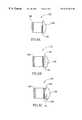
- FIGS. 1A-1Cshow schematics of image shutters, in accordance with preferred embodiments of the present invention, with dimensions greatly exaggerated and not to scale for ease and clarity of presentation;
- FIG. 2shows schematically an array of three image shutters used to form a compound image shutter, in accordance with a preferred embodiment of the present invention
- FIG. 3shows schematically two image shutters aligned collinear, in accordance with a preferred embodiment of the present invention, to provide very short, fast rise time, light pulses;
- FIG. 4shows a schematic of a multiple wavelength image shutter for modulating light in four different wavelength bands, in accordance with a preferred embodiment of the present invention
- FIGS. 5A-5Cshow schematically hybrid optical components in accordance with preferred embodiments of the present invention.
- FIGS. 6A-6Cshow schematically modular optical devices in accordance with a preferred embodiment of the present invention.
- FIGS. 1A-1Cshow image shutters 20 , 22 and 24 , in accordance with preferred embodiments of the present invention. In these figures dimensions are greatly exaggerated and not to scale for ease and clarity of presentation.
- Image shutter 20shown in FIG. 1A, comprises an epitaxial MQW structure 26 between heavily p doped layers 28 and n doped layers 30 to form a pin diode structure.
- MQW structure 26comprises a multiplicity of narrow gap semiconductor layers 32 alternating with wide gap semiconductor layers 34 .
- Various compounds of III-V elementsmay be used to form layers 32 and 34 in MQW structure 26 .
- layers 32are all of the same thickness.
- the thickness of layers 32is substantially less than the diameter of excitons in layers 32 .
- wide gap layers 34are thick enough so that wave functions of electrons and holes confined in one narrow gap layer (i.e.
- a quantum well of MQW 26are substantially uncoupled from wave functions of particles in adjacent layers of MQW 26 .
- the energy of the absorption edge of the MQW structure 26 and thereby the operating wavelengths of image shutter 20can be varied by changing which elements are used to form narrow gap layers 32 , the mole fractions of the elements and the thickness of the layers.
- Image shutter 20Light enters image shutter 20 through a first aperture 36 on a first end surface 38 of image shutter 20 , travels through image shutter 20 substantially perpendicular to the planes of layers 32 and 34 in MQW structure 26 and exits through a second aperture 36 (not shown), preferably identical to and parallel to first aperture 36 , on a second end surface 40 of image shutter 20 .
- First end surface 38is preferably a surface area of a thick heavily p doped semiconductor layer 42 .
- Second end surface 40is preferably a surface area of a thick heavily n doped semiconductor layer 44 . While image shutter 20 is shown having a square cross section and first aperture 36 is square, other convenient cross sections and aperture shapes are possible and advantageous.
- First and second apertures 36are preferably coated with an antireflective coating by processes known in the art so that light at an operating wavelength of image shutter 20 enters and exits image shutter 20 with very little insertion and exit loss.
- the sum of insertion and exit lossis less than 5%. More preferably the sum is less than 1%. Most preferably the sum is less than 0.5%.
- the area of first and second apertures 36is greater than 4 mm 2 . More preferably the area of first and second apertures 36 is greater than 9 mm 2 . Most preferably the area of first and second apertures 36 is greater than 16 mm 2 .
- Each of first and second apertures 36is preferably surrounded by a driving electrode 46 configured in the shape of a “picture frame” (only driving electrode 46 surrounding first aperture 36 is shown).
- Driving electrodes 46are bonded to end surfaces 38 and 40 by methods known in the art. Voltage differences applied between driving electrodes 46 at end surfaces 38 and 40 create an electric field in MQW structure 26 and cause image shutter 20 to attenuate light at operating wavelengths of image shutter 20 . Voltage differences are preferably applied between driving electrodes 46 by using a multiport electrification scheme whereby each driving electrode 46 is simultaneously electrified at a plurality of points along edges of the driving electrode 46 . This is preferably accomplished using FETs or emitter followers, 47 formed on the substrate immediately outside of electrode 46 . The geometry of driving electrodes 46 and the multiport electrification scheme reduce the rise time of image shutter 20 .
- narrow gap layers 32are formed from GaAs and wide gap layers 34 are formed from Al x Ga (1 ⁇ x) As.
- Heavily p doped layers 28preferably comprise layers 50 and 52 which are respectively 400 nm of Al x Ga (1 ⁇ x) As(p ++ ) and 20 nm of GaAs(p ++ ).
- Heavily n doped layers 30preferably comprise layers 54 , 56 and 58 which are respectively 300 nm of Al x Ga (1 ⁇ x) As(n ++ ), 20 nm of GaAs(n ++ ) and 100 nm of Al x Ga (1 ⁇ x) As(n ++ ).
- doping levels of layers 28 and 30are greater than 10 19 /cm 3 .
- the thickness of narrow gap and wide gap layersare 10 nm and 8 nm respectively.
- the multiplicity of narrow gap layers 32 in MQW structure 20is preferably greater than 100.
- image shutter 20provides an on/off ratio of 20 for operating wavelengths near 860 nm. It should be realized that the values for the mole ratios, the thickness of the different layers and doping levels noted above are examples and that values for these parameters different from the values noted are possible and can be advantageous.
- FIG. 1Bshows a schematic of an image shutter 22 , in accordance with a second preferred embodiment of the present invention.
- Image shutter 22is similar to image shutter 20 except for driving electrodes 60 (only one of which is shown) on surfaces 38 and 40 which are in place of driving electrodes 46 of image shutter 20 .
- Each driving electrode 60comprises a conducting “picture frame” 62 and a mesh 64 of conducting wires 66 .
- a driving electrode 60is placed on each of apertures 36 (only one of which is shown) of image shutter 22 so that picture frame 62 surrounds the aperture 36 and conducting mesh 64 covers the surface of the aperture 36 .
- conducting wires 66are formed from transparent conducting material.
- driving electrodes 62are preferably electrified in a multiport electrification scheme using FETs or emitter followers 47 formed on the substrate immediately outside of electrode 62 .
- FIG. 1Cshows a schematic of an image shutter 24 similar to image shutters 20 and 22 in which driving electrodes on apertures 36 are divided electrodes 70 (only one of which is shown).
- Each divided electrode 70comprises a plurality of sector electrodes 72 wherein each sector electrode 72 covers a different region of the aperture 36 on which the divided electrode 70 is placed.
- divided electrodes 70 on each of apertures 36 on opposite faces 38 and 40are identical and oriented with respect to each other so that they are mirror images of each other.
- Image shutter 24is operated by applying voltage differences between pairs of sector electrodes 72 , where a pair of sector electrodes comprises a sector electrode 72 on one aperture 36 and its mirror image sector electrode 72 (not shown) on the opposite aperture 36 .
- Pairs of sector electrodes 72are preferably driven independently of each other with controllable small delay times between voltages applied to pairs of sector electrodes 72 .
- the capacitance of a single sector electrode pairis approximately equal to the capacitance of image shutter 24 divided by the number of sector electrodes 72 in a divided electrode 70 .
- the sector electrode pairsessentially divide up the capacitance of image shutter 24 between them. Image shutter 24 can therefore be operated with a much faster rise time by driving individual sector electrodes 72 through independent power sources (not shown) than by driving image shutter 24 with two single large electrodes one on each of end surfaces 36 .
- Divided electrodes 70comprise at least two sector electrodes 72 .
- Divided electrode 72 in FIG. 1Cis shown having six sector electrodes 72 .
- Each sector electrode 72is preferably a small planar conductor formed from a transparent conducting material.
- each sector electrode 72comprises a small conducting wire or loop.
- the conducting wire or loopis formed from a transparent conducting material.
- Each sector electrode 72is preferably driven by its own FET or emitter follower 47 formed on the same semiconductor layers to which divided electrodes 70 are bonded. It should be understood that geometries other than that shown in FIG. 1C for the shape and dispostion of sector electrodes 72 are possible and advantageous.
- sector electrodes 72can be crescent shaped and arranged in concentric circles.
- a multiplicity of image shuttersin accordance with a preferred embodiment of the present invention, can be aligned collinear alone a common axis perpendicular to the surfaces of their apertures to form a compound shutter.
- light entering an aperture of a first of the aligned image shutterspasses through all the image shutters.
- a compound shutter in accordance with a preferred embodiment of the present inventioncan be used to provide image shutters that operate at very high on/off transmission ratios and low voltages.
- a compound shutter in accordance with a preferred embodiment of the present inventioncomprises a multiplicity of N shutters, wherein each shutter of the multiplicity of shutters provides an on/off transmission ratio of CR for a voltage change of V, the compound shutter provides an on/off transmission ratio of CR N for the same voltage change V.
- FIG. 2shows schematically an example where a multiplicity of three image shutters 20 as shown in FIG. 1A, having an on/off transmission ratio of 7, are bonded together to form a compound image shutter 100 .
- Driving electrodes 46which are adjacent to each other in compound image shutter 100 , are preferably driven at the same voltage.
- image shutters other than image shutter 20in accordance with different preferred embodiments of the present invention, such as image shutters 22 and 24 in FIGS. 1B and 1C, respectively, can be used to form compound image shutters.
- image shutter 20 to form compound image shutter 100 in FIG. 2is by way of example.
- Compound image shuttersin accordance with a preferred embodiment of the present invention, can also be used to modulate light by transmitting light at intensities which are predetermined fractions of intensities of incident light having a wavelength equal to an operational wavelength of the compound image shutter.
- each of image shutters 20 comprised in compound shutter 100has an on/off transmission ratio of 2, compound shutter 100 can be used to transmit light at intensities of ⁇ 1, 1 ⁇ 2, 1 ⁇ 4 and 1 ⁇ 8 times the intensity of light incident on compound shutter 100 .
- FIG. 3shows two image shutters 160 and 162 of the types shown in FIGS. 1A-1C colinearly aligned along an axis 163 perpendicular to their apertures 36 , in accordance with a preferred embodiment of the present invention, to provide very short, fast rise time, light pulses.
- Curve 164represents the “open/close” status of shutter 160 .
- Raised part 166 of curve 164indicates when shutter 160 is open and lowered part 168 of curve 164 indicates when shutter 160 is closed.
- curve 170represents the open/close status of shutter 162 .
- Raised and lowered parts 172 and 174 respectively of curve 170indicate when shutter 162 is open and closed.
- shutter 162switches from being open to being closed.
- Lightcan pass through both shutters 160 and 162 from one side of shutters 160 and 162 to the other side of shutters 160 and 162 only when both are simultaneously open. This occurs from time t 1 to time t 2 .
- Curve 176represents the open/close status of shutters 160 and 162 acting together.
- Raised part 178 of curve 176represents the time period t 1 ⁇ t 2 during which shutters 160 and 162 simultaneously transmit light.
- Light, indicated by wavy arrow 180which is incident on shutter 160 in the direction of shutter 162 will be transmitted during the time both shutters are open to form a pulse of light (t 2 ⁇ t 1 ) seconds long.
- shutters 160 and 162Since the absorption edge of the multiple quantum well structure of shutters 160 and 162 is very steep, shutters 160 and 162 switch from a state of transmission to a state of no transmission during a very short period of time during the rise time of the electric field applied to shutters 160 or 162 . The switching time can therefore be made shorter than the electrical rise time of shutters 160 and 162 . As a result by operating shutters 160 and 162 , in accordance with a preferred embodiment of the present invention, as shown by way of example in FIG. 3, very short well defined pulses of light can be produced.
- a multiplicity of image shuttersin accordance with a preferred embodiment of the present invention, can be used to provide a multi-wavelength shutter that modulates light in a plurality of different wavelength bands.
- Each of the multiplicity of image shuttershas one aperture, a front aperture, covered with a selective reflecting coating that transmits light having a wavelength in a different one of the plurality of wavelength bands that the multi-wavelength shutter modulates.
- the other aperture, a back aperture, of each image shutteris covered with a reflecting coating that reflects light having a wavelength in the wavelength band that the reflecting coating on the front aperture of the image shutter transmits.
- the multiplicity of image shutters in the multi-wavelength shutterare arranged with respect to each other so that light that is incident on the multi-wavelength shutter is reflected from the front aperture of each of the multiplicity of image shutters before the light can exit the multi-wavelength shutter.
- light in any particular wavelength band of the multiwavelength shutteris selectively shuttered or modulated by the multi-wavelength shutter by controlling the image shutter that has its front aperture coated with the reflecting coating that transmits light in that particular wavelength band.
- the number of different wavelength bands modulated by the multi-wavelength shutteris equal to or less than the number of the image shutters comprised in the wavelength shutter.
- FIG. 4shows a schematic of a multi-wavelength shutter 200 , in accordance with a preferred embodiment of the present invention, for modulating four different wavelength bands of light, referred to as wavelength bands ⁇ 1 , ⁇ 2 , ⁇ 3 and ⁇ 4 respectively.
- Multi-wavelength shutter 200comprises four different image shutters 201 , 202 , 203 and 204 .
- Each image shutter 201 , 202 , 203 and 204has a front aperture 206 and a back aperture 208 .
- Front apertures 206 and back apertures 208 of image shutters 201 , 202 , 203 and 204are covered with reflecting coatings (not shown).
- the reflecting coatings on front apertures 206 of image shutters 201 , 202 , 203 and 204transmit light in wavelength bands ⁇ 1 , ⁇ 2 , ⁇ 3 and ⁇ 4 respectively (shown FIG. 4 in parenthesis beside numerals 201 , 202 , 203 and 204 respectively) and reflect light in any of the other wavelength bands.
- the reflecting coatings on back apertures 208 of image shutters 201 , 202 , 203 and 204reflect light in wavelength bands ⁇ 1 , ⁇ 2 , ⁇ 3 and ⁇ 4 respectively.
- Image shutters 201 , 202 , 203 and 204are oriented with respect to each other so that light incident on front aperture 206 of image shutter 201 must reflect from front surfaces 206 of image shutters 202 , 203 and 204 also in order to be transmitted through multi-wavelength shutter 200 .
- Shown in FIG. 4are four light rays 211 , 212 , 213 and 214 that are incident on front surface 206 of image shutter 201 .
- Light rays 211 , 212 , 213 and 214have wavelengths in wavelength bands ⁇ 1 , ⁇ 2 , ⁇ 3 and ⁇ 4 respectively (shown FIG. 4 in parenthesis beside numerals 211 , 212 , 213 and 214 respectively).
- Each of image shutters 201 , 202 , 203 and 204is open and each of light rays 211 , 212 , 213 and 214 is transmitted through multi-wavelength shutter 200 .
- Light rays 211 , 212 , 213 and 214are reflected from back apertures 208 of image shutters 201 , 202 , 203 and 204 respectively. If image shutter 201 , 202 , 203 or 204 is closed then light ray 211 , 212 , 213 or 214 respectively will stop being transmitted.
- FIGS. 5A-5Cshow hybrid optical components 110 , 112 and 114 in accordance with preferred embodiments of the present invention.
- FIG. 5Ashows hybrid optical component 110 comprising an image shutter 20 , in accordance with a preferred embodiment of the present invention, bonded to a lens 120 .
- FIG. 5Bshows hybrid optical component 112 comprising an image shutter 20 , in accordance with a preferred embodiment of the present invention, bonded to a light sensitive device 122 such as a CMOS-CCD.
- FIG. 5Cshows hybrid component 114 , which comprises an image shutter 20 bonded to a mirror 124 , in accordance with a preferred embodiment of the present invention.
- Lightshown schematically by arrows 126 enters hybrid component 114 and is reflected by mirror 124 .
- the on/off transmission ratio achieved by hybrid component 114is the square of the on/off transmission ratio available from transmission components in which light passes through MQW structure 26 once.
- FIGS. 6A-6Cshow modular optical devices in accordance with preferred embodiments of the present invention.
- FIG. 6Ashows a device 130 which comprises an image shutter 20 combined with a lens 136 and an image sensing device 138 such as a CMOS-CCD located at the focal plane of lens 136 , in accordance with a preferred embodiment of the present invention.
- FIG. 6Bshows a device 132 which comprises an image shutter 20 having light sources 140 such as LEDs or lasers grown on one of the outermost semiconductor layers of image shutter 20 combined with a lens 136 and an image sensing device 138 , in accordance with a preferred embodiment of the present invention.
- FIG. 1Ashows a device 130 which comprises an image shutter 20 combined with a lens 136 and an image sensing device 138 such as a CMOS-CCD located at the focal plane of lens 136 , in accordance with a preferred embodiment of the present invention.
- FIG. 6Bshows a device 132 which comprises an image shutter 20 having light sources 140 such as LEDs or
- FIG. 6Cshows a device 134 comprising an image shutter 20 grown together as a single unit with light sources 140 and FETs 150 for controlling both light sources and image shutter switches in accordance with a preferred embodiment of the present invention.
- Image shutter 20is combined with lens 136 and image sensing device 138 to form a complete modular device.
- Device 134can be used as an optical range camera similar to the optical range camera described in PCT patent application PCT/IL96/00020.
Landscapes
- Physics & Mathematics (AREA)
- Chemical & Material Sciences (AREA)
- Optics & Photonics (AREA)
- Nonlinear Science (AREA)
- Engineering & Computer Science (AREA)
- Nanotechnology (AREA)
- General Physics & Mathematics (AREA)
- Life Sciences & Earth Sciences (AREA)
- Biophysics (AREA)
- Crystallography & Structural Chemistry (AREA)
- Optical Modulation, Optical Deflection, Nonlinear Optics, Optical Demodulation, Optical Logic Elements (AREA)
- Facsimile Heads (AREA)
- Electrochromic Elements, Electrophoresis, Or Variable Reflection Or Absorption Elements (AREA)
Abstract
Description
Claims (34)
Applications Claiming Priority (1)
| Application Number | Priority Date | Filing Date | Title |
|---|---|---|---|
| PCT/IL1998/000060WO1999040478A1 (en) | 1998-02-08 | 1998-02-08 | Large aperture optical image shutter |
Publications (1)
| Publication Number | Publication Date |
|---|---|
| US6331911B1true US6331911B1 (en) | 2001-12-18 |
Family
ID=11062306
Family Applications (1)
| Application Number | Title | Priority Date | Filing Date |
|---|---|---|---|
| US09/601,805Expired - Fee RelatedUS6331911B1 (en) | 1998-02-08 | 1998-02-08 | Large aperture optical image shutter |
Country Status (7)
| Country | Link |
|---|---|
| US (1) | US6331911B1 (en) |
| EP (1) | EP1055146B1 (en) |
| JP (1) | JP4195189B2 (en) |
| AU (1) | AU5876798A (en) |
| DE (1) | DE69810968T2 (en) |
| ES (1) | ES2194302T3 (en) |
| WO (1) | WO1999040478A1 (en) |
Cited By (68)
| Publication number | Priority date | Publication date | Assignee | Title |
|---|---|---|---|---|
| US20040017473A1 (en)* | 2002-07-27 | 2004-01-29 | Sony Computer Entertainment Inc. | Man-machine interface using a deformable device |
| US20050107979A1 (en)* | 2003-11-04 | 2005-05-19 | Buermann Dale H. | Apparatus and method for determining an inclination of an elongate object contacting a plane surface |
| US20050280801A1 (en)* | 2003-10-09 | 2005-12-22 | Gonzalez-Banos Hector H | Systems and methods for determining depth using shuttered light pulses |
| US20070276256A1 (en)* | 2005-02-17 | 2007-11-29 | 3Dv Systems Ltd. | Method and apparatus for imaging tissues |
| US7623115B2 (en) | 2002-07-27 | 2009-11-24 | Sony Computer Entertainment Inc. | Method and apparatus for light input device |
| US7627139B2 (en) | 2002-07-27 | 2009-12-01 | Sony Computer Entertainment Inc. | Computer image and audio processing of intensity and input devices for interfacing with a computer program |
| US7646372B2 (en) | 2003-09-15 | 2010-01-12 | Sony Computer Entertainment Inc. | Methods and systems for enabling direction detection when interfacing with a computer program |
| US7663689B2 (en) | 2004-01-16 | 2010-02-16 | Sony Computer Entertainment Inc. | Method and apparatus for optimizing capture device settings through depth information |
| US20100053592A1 (en)* | 2007-01-14 | 2010-03-04 | Microsoft International Holdings B.V. | Method, device and system for imaging |
| US20100163889A1 (en)* | 2008-12-31 | 2010-07-01 | Samsung Electronics Co., Ltd. | Optical modulator with pixelization patterns |
| US20100171813A1 (en)* | 2009-01-04 | 2010-07-08 | Microsoft International Holdings B.V. | Gated 3d camera |
| US20100177372A1 (en)* | 2009-01-15 | 2010-07-15 | Samsung Electronics Co., Ltd. | Optical image modulator, optical apparatus including the same, and methods of manufacturing and operating the optical image modulator |
| US7760248B2 (en) | 2002-07-27 | 2010-07-20 | Sony Computer Entertainment Inc. | Selective sound source listening in conjunction with computer interactive processing |
| US20100182671A1 (en)* | 2009-01-19 | 2010-07-22 | Samsung Electronics Co., Ltd. | Optical image shutter |
| US20100321755A1 (en)* | 2009-06-17 | 2010-12-23 | Samsung Electronics Co., Ltd. | Optical modulator, methods of manufacturing and operating the same and optical apparatus including the optical modulator |
| US7874917B2 (en) | 2003-09-15 | 2011-01-25 | Sony Computer Entertainment Inc. | Methods and systems for enabling depth and direction detection when interfacing with a computer program |
| US7883415B2 (en) | 2003-09-15 | 2011-02-08 | Sony Computer Entertainment Inc. | Method and apparatus for adjusting a view of a scene being displayed according to tracked head motion |
| US20110074659A1 (en)* | 2008-12-24 | 2011-03-31 | Samsung Electronics Co., Ltd. | High speed optical shutter, method of operating the same and apparatus including the same |
| US20110176709A1 (en)* | 2010-01-21 | 2011-07-21 | Samsung Electronics Co., Ltd. | Method and apparatus for calculating a distance between an optical apparatus and an object |
| US20110181936A1 (en)* | 2010-01-22 | 2011-07-28 | Samsung Electronics Co., Ltd. | Optical modulator |
| US20110187826A1 (en)* | 2010-02-03 | 2011-08-04 | Microsoft Corporation | Fast gating photosurface |
| US8035629B2 (en) | 2002-07-18 | 2011-10-11 | Sony Computer Entertainment Inc. | Hand-held computer interactive device |
| US8072470B2 (en) | 2003-05-29 | 2011-12-06 | Sony Computer Entertainment Inc. | System and method for providing a real-time three-dimensional interactive environment |
| US8142288B2 (en) | 2009-05-08 | 2012-03-27 | Sony Computer Entertainment America Llc | Base station movement detection and compensation |
| US8287373B2 (en) | 2008-12-05 | 2012-10-16 | Sony Computer Entertainment Inc. | Control device for communicating visual information |
| US8310656B2 (en) | 2006-09-28 | 2012-11-13 | Sony Computer Entertainment America Llc | Mapping movements of a hand-held controller to the two-dimensional image plane of a display screen |
| US8313380B2 (en) | 2002-07-27 | 2012-11-20 | Sony Computer Entertainment America Llc | Scheme for translating movements of a hand-held controller into inputs for a system |
| US8323106B2 (en) | 2008-05-30 | 2012-12-04 | Sony Computer Entertainment America Llc | Determination of controller three-dimensional location using image analysis and ultrasonic communication |
| US8342963B2 (en) | 2009-04-10 | 2013-01-01 | Sony Computer Entertainment America Inc. | Methods and systems for enabling control of artificial intelligence game characters |
| US8368753B2 (en) | 2008-03-17 | 2013-02-05 | Sony Computer Entertainment America Llc | Controller with an integrated depth camera |
| US8393964B2 (en) | 2009-05-08 | 2013-03-12 | Sony Computer Entertainment America Llc | Base station for position location |
| US8432599B2 (en) | 2010-12-03 | 2013-04-30 | Samsung Electronics Co., Ltd. | Optical image modulator and method of manufacturing the same |
| US8527657B2 (en) | 2009-03-20 | 2013-09-03 | Sony Computer Entertainment America Llc | Methods and systems for dynamically adjusting update rates in multi-player network gaming |
| US8542907B2 (en) | 2007-12-17 | 2013-09-24 | Sony Computer Entertainment America Llc | Dynamic three-dimensional object mapping for user-defined control device |
| US8547401B2 (en) | 2004-08-19 | 2013-10-01 | Sony Computer Entertainment Inc. | Portable augmented reality device and method |
| US8570378B2 (en) | 2002-07-27 | 2013-10-29 | Sony Computer Entertainment Inc. | Method and apparatus for tracking three-dimensional movements of an object using a depth sensing camera |
| KR101353892B1 (en)* | 2009-07-30 | 2014-01-20 | 모토로라 모빌리티 엘엘씨 | Solid state shutter devices and methods |
| US8686939B2 (en) | 2002-07-27 | 2014-04-01 | Sony Computer Entertainment Inc. | System, method, and apparatus for three-dimensional input control |
| US8781151B2 (en) | 2006-09-28 | 2014-07-15 | Sony Computer Entertainment Inc. | Object detection using video input combined with tilt angle information |
| US8797260B2 (en) | 2002-07-27 | 2014-08-05 | Sony Computer Entertainment Inc. | Inertially trackable hand-held controller |
| US8840470B2 (en) | 2008-02-27 | 2014-09-23 | Sony Computer Entertainment America Llc | Methods for capturing depth data of a scene and applying computer actions |
| US8902411B2 (en) | 2010-12-23 | 2014-12-02 | Samsung Electronics Co., Ltd. | 3-dimensional image acquisition apparatus and method of extracting depth information in the 3D image acquisition apparatus |
| US8961313B2 (en) | 2009-05-29 | 2015-02-24 | Sony Computer Entertainment America Llc | Multi-positional three-dimensional controller |
| US9051178B2 (en) | 2012-01-05 | 2015-06-09 | Gwangju Institute Of Science And Technology | Transmissive image modulator including stacked diode structure having multi absorption modes |
| US9082909B2 (en) | 2013-01-04 | 2015-07-14 | Samsung Electronics Co., Ltd. | Optical device including three coupled quantum well structure |
| US9123164B2 (en) | 2012-02-07 | 2015-09-01 | Samsung Electronics Co., Ltd. | 3D image acquisition apparatus and method of extracting depth information in 3D image acquisition apparatus |
| US20150304535A1 (en)* | 2014-02-21 | 2015-10-22 | Samsung Electronics Co., Ltd. | Multi-band biometric camera system having iris color recognition |
| US9177387B2 (en) | 2003-02-11 | 2015-11-03 | Sony Computer Entertainment Inc. | Method and apparatus for real time motion capture |
| US9182614B2 (en) | 2012-04-12 | 2015-11-10 | Samsung Electronics Co., Ltd. | Large-area transmissive type optical image modulator and method of manufacturing the same and optical apparatus including transmissive type optical image modulator |
| US9190545B2 (en) | 2013-11-07 | 2015-11-17 | Samsung Electronics Co., Ltd. | Optical device including three-coupled quantum well structure having multi-energy level |
| US20160057404A1 (en)* | 2014-08-19 | 2016-02-25 | Samsung Electronics Co., Ltd. | Transmissive optical shutter and method of fabricating the same |
| US20160073088A1 (en)* | 2014-09-08 | 2016-03-10 | David Cohen | Variable resolution pixel |
| US9310488B2 (en) | 2010-09-17 | 2016-04-12 | Samsung Electronics Co., Ltd. | Apparatus and method for generating depth image |
| US9393487B2 (en) | 2002-07-27 | 2016-07-19 | Sony Interactive Entertainment Inc. | Method for mapping movements of a hand-held controller to game commands |
| US9418425B2 (en) | 2011-10-25 | 2016-08-16 | Samsung Electronic Co., Ltd. | 3D image acquisition apparatus and method of calculating depth information in the 3D image acquisition apparatus |
| US9474968B2 (en) | 2002-07-27 | 2016-10-25 | Sony Interactive Entertainment America Llc | Method and system for applying gearing effects to visual tracking |
| US9573056B2 (en) | 2005-10-26 | 2017-02-21 | Sony Interactive Entertainment Inc. | Expandable control device via hardware attachment |
| US9638941B2 (en) | 2011-05-24 | 2017-05-02 | Samsung Electronics Co., Ltd. | Photonic crystal type light modulator and 3D image acquisition apparatus employing the same |
| US9682319B2 (en) | 2002-07-31 | 2017-06-20 | Sony Interactive Entertainment Inc. | Combiner method for altering game gearing |
| US9749613B2 (en) | 2013-04-08 | 2017-08-29 | Samsung Electronics Co., Ltd. | 3D image acquisition apparatus and method of generating depth image in the 3D image acquisition apparatus |
| US9841617B2 (en) | 2014-04-04 | 2017-12-12 | Gwangju Institute Of Science And Technology | Optical device including three-coupled quantum well structure |
| US9894347B2 (en) | 2013-05-22 | 2018-02-13 | Samsung Electronics Co., Ltd. | 3D image acquisition apparatus and method of driving the same |
| US10205933B2 (en) | 2014-08-29 | 2019-02-12 | Samsung Electronics Co., Ltd. | Depth image acquisition apparatus and method of acquiring depth information |
| US10279254B2 (en) | 2005-10-26 | 2019-05-07 | Sony Interactive Entertainment Inc. | Controller having visually trackable object for interfacing with a gaming system |
| US10367332B2 (en) | 2015-10-08 | 2019-07-30 | Samsung Electronics Co., Ltd. | Edge emitting laser light source and 3D image obtaining apparatus including the same |
| US10509125B2 (en) | 2015-12-24 | 2019-12-17 | Samsung Electronics Co., Ltd. | Method and device for acquiring distance information |
| US10545237B2 (en) | 2016-08-22 | 2020-01-28 | Samsung Electronics Co., Ltd. | Method and device for acquiring distance information |
| USRE48417E1 (en) | 2006-09-28 | 2021-02-02 | Sony Interactive Entertainment Inc. | Object direction using video input combined with tilt angle information |
Families Citing this family (6)
| Publication number | Priority date | Publication date | Assignee | Title |
|---|---|---|---|---|
| AU9456198A (en) | 1998-09-28 | 2000-04-17 | 3Dv Systems Ltd. | Distance measurement with a camera |
| ATE285079T1 (en)* | 1999-09-08 | 2005-01-15 | 3Dv Systems Ltd | 3D IMAGE PRODUCTION SYSTEM |
| US7196390B1 (en) | 1999-09-26 | 2007-03-27 | 3Dv Systems Ltd. | Solid state image wavelength converter |
| WO2002061498A1 (en) | 2001-01-30 | 2002-08-08 | 3Dv Systems, Ltd. | Optical modulator |
| WO2003001282A1 (en)* | 2001-06-26 | 2003-01-03 | 3Dv Systems, Ltd. | Compound optical modulator |
| WO2009078003A1 (en)* | 2007-12-19 | 2009-06-25 | Microsoft International Holdings B.V. | An image sensor and a configuration for improved skew time |
Citations (7)
| Publication number | Priority date | Publication date | Assignee | Title |
|---|---|---|---|---|
| US4525687A (en) | 1983-02-28 | 1985-06-25 | At&T Bell Laboratories | High speed light modulator using multiple quantum well structures |
| JPS62226130A (en) | 1986-03-27 | 1987-10-05 | Seiko Epson Corp | lcd light shutter |
| JPH03132717A (en) | 1989-10-19 | 1991-06-06 | Fujitsu General Ltd | Electrode structure of PLZT display device |
| US5307200A (en)* | 1992-04-14 | 1994-04-26 | Ricoh Company, Ltd. | Semiconductor optical device having an optical confinement structure |
| US5412499A (en)* | 1993-03-29 | 1995-05-02 | At&T Corp. | Spatial light modulator using quantum well material |
| US5455451A (en)* | 1989-08-18 | 1995-10-03 | Hitachi, Ltd. | Superconductized semiconductor device using penetrating Cooper pairs |
| WO1997001111A2 (en) | 1995-06-22 | 1997-01-09 | 3Dv Systems Ltd. | Improved optical ranging camera |
Family Cites Families (1)
| Publication number | Priority date | Publication date | Assignee | Title |
|---|---|---|---|---|
| JPS63177109A (en)* | 1987-01-19 | 1988-07-21 | Hitachi Ltd | optical element |
- 1998
- 1998-02-08WOPCT/IL1998/000060patent/WO1999040478A1/enactiveIP Right Grant
- 1998-02-08EPEP98902160Apatent/EP1055146B1/ennot_activeExpired - Lifetime
- 1998-02-08AUAU58767/98Apatent/AU5876798A/ennot_activeWithdrawn
- 1998-02-08USUS09/601,805patent/US6331911B1/ennot_activeExpired - Fee Related
- 1998-02-08ESES98902160Tpatent/ES2194302T3/ennot_activeExpired - Lifetime
- 1998-02-08JPJP2000530831Apatent/JP4195189B2/ennot_activeExpired - Lifetime
- 1998-02-08DEDE69810968Tpatent/DE69810968T2/ennot_activeExpired - Lifetime
Patent Citations (7)
| Publication number | Priority date | Publication date | Assignee | Title |
|---|---|---|---|---|
| US4525687A (en) | 1983-02-28 | 1985-06-25 | At&T Bell Laboratories | High speed light modulator using multiple quantum well structures |
| JPS62226130A (en) | 1986-03-27 | 1987-10-05 | Seiko Epson Corp | lcd light shutter |
| US5455451A (en)* | 1989-08-18 | 1995-10-03 | Hitachi, Ltd. | Superconductized semiconductor device using penetrating Cooper pairs |
| JPH03132717A (en) | 1989-10-19 | 1991-06-06 | Fujitsu General Ltd | Electrode structure of PLZT display device |
| US5307200A (en)* | 1992-04-14 | 1994-04-26 | Ricoh Company, Ltd. | Semiconductor optical device having an optical confinement structure |
| US5412499A (en)* | 1993-03-29 | 1995-05-02 | At&T Corp. | Spatial light modulator using quantum well material |
| WO1997001111A2 (en) | 1995-06-22 | 1997-01-09 | 3Dv Systems Ltd. | Improved optical ranging camera |
Non-Patent Citations (5)
| Title |
|---|
| Fujitsu General Ltd.; Patent Abstracts of Japan; vol. 015; No. 349 (P-1247); Sep. 4, 1991 & JP 03-132717 A; Jun. 1991. |
| Miller, D. et al.; "Band-Edge Electroabsorption in Quantum Well Structures: The Quantum-Confined Stark Effect"; Physical Review Letter; vol. 56; No. 22; pp. 2173-2176; Nov. 26, 1984. |
| Miller, D. et al.; "Electric Field Dependence of Optical Absorption Near Band Gap of Quantum-Well Structures"; Physical Review B; vol. 32; No. 2; pp. 1043-1060; Jul. 15, 1985. |
| Seiko Epson Corp.; Patent Abstracts of Japan; vol. 012; No. 093 (P-680); Mar. 26, 1988 & JP 62-226130 A; Oct. 5, 1987. |
| Wood, T. et al.; "High Speed Optical Modulation with GaAs/GaAIAs Quantum Wells in a p-i-n Diode Structure"; Appli Phyical Letter; 44(1); pp. 16-18; Jan. 1, 1984. |
Cited By (103)
| Publication number | Priority date | Publication date | Assignee | Title |
|---|---|---|---|---|
| US8035629B2 (en) | 2002-07-18 | 2011-10-11 | Sony Computer Entertainment Inc. | Hand-held computer interactive device |
| US9682320B2 (en) | 2002-07-22 | 2017-06-20 | Sony Interactive Entertainment Inc. | Inertially trackable hand-held controller |
| US7627139B2 (en) | 2002-07-27 | 2009-12-01 | Sony Computer Entertainment Inc. | Computer image and audio processing of intensity and input devices for interfacing with a computer program |
| US10099130B2 (en) | 2002-07-27 | 2018-10-16 | Sony Interactive Entertainment America Llc | Method and system for applying gearing effects to visual tracking |
| US7102615B2 (en) | 2002-07-27 | 2006-09-05 | Sony Computer Entertainment Inc. | Man-machine interface using a deformable device |
| US8313380B2 (en) | 2002-07-27 | 2012-11-20 | Sony Computer Entertainment America Llc | Scheme for translating movements of a hand-held controller into inputs for a system |
| US9474968B2 (en) | 2002-07-27 | 2016-10-25 | Sony Interactive Entertainment America Llc | Method and system for applying gearing effects to visual tracking |
| US7623115B2 (en) | 2002-07-27 | 2009-11-24 | Sony Computer Entertainment Inc. | Method and apparatus for light input device |
| US8686939B2 (en) | 2002-07-27 | 2014-04-01 | Sony Computer Entertainment Inc. | System, method, and apparatus for three-dimensional input control |
| US7639233B2 (en) | 2002-07-27 | 2009-12-29 | Sony Computer Entertainment Inc. | Man-machine interface using a deformable device |
| US8188968B2 (en) | 2002-07-27 | 2012-05-29 | Sony Computer Entertainment Inc. | Methods for interfacing with a program using a light input device |
| US10406433B2 (en) | 2002-07-27 | 2019-09-10 | Sony Interactive Entertainment America Llc | Method and system for applying gearing effects to visual tracking |
| US20040017473A1 (en)* | 2002-07-27 | 2004-01-29 | Sony Computer Entertainment Inc. | Man-machine interface using a deformable device |
| US8570378B2 (en) | 2002-07-27 | 2013-10-29 | Sony Computer Entertainment Inc. | Method and apparatus for tracking three-dimensional movements of an object using a depth sensing camera |
| US9381424B2 (en) | 2002-07-27 | 2016-07-05 | Sony Interactive Entertainment America Llc | Scheme for translating movements of a hand-held controller into inputs for a system |
| US8797260B2 (en) | 2002-07-27 | 2014-08-05 | Sony Computer Entertainment Inc. | Inertially trackable hand-held controller |
| US8976265B2 (en) | 2002-07-27 | 2015-03-10 | Sony Computer Entertainment Inc. | Apparatus for image and sound capture in a game environment |
| US10220302B2 (en) | 2002-07-27 | 2019-03-05 | Sony Interactive Entertainment Inc. | Method and apparatus for tracking three-dimensional movements of an object using a depth sensing camera |
| US9393487B2 (en) | 2002-07-27 | 2016-07-19 | Sony Interactive Entertainment Inc. | Method for mapping movements of a hand-held controller to game commands |
| US7760248B2 (en) | 2002-07-27 | 2010-07-20 | Sony Computer Entertainment Inc. | Selective sound source listening in conjunction with computer interactive processing |
| US9682319B2 (en) | 2002-07-31 | 2017-06-20 | Sony Interactive Entertainment Inc. | Combiner method for altering game gearing |
| US9177387B2 (en) | 2003-02-11 | 2015-11-03 | Sony Computer Entertainment Inc. | Method and apparatus for real time motion capture |
| US11010971B2 (en) | 2003-05-29 | 2021-05-18 | Sony Interactive Entertainment Inc. | User-driven three-dimensional interactive gaming environment |
| US8072470B2 (en) | 2003-05-29 | 2011-12-06 | Sony Computer Entertainment Inc. | System and method for providing a real-time three-dimensional interactive environment |
| US7883415B2 (en) | 2003-09-15 | 2011-02-08 | Sony Computer Entertainment Inc. | Method and apparatus for adjusting a view of a scene being displayed according to tracked head motion |
| US7874917B2 (en) | 2003-09-15 | 2011-01-25 | Sony Computer Entertainment Inc. | Methods and systems for enabling depth and direction detection when interfacing with a computer program |
| US8758132B2 (en) | 2003-09-15 | 2014-06-24 | Sony Computer Entertainment Inc. | Methods and systems for enabling depth and direction detection when interfacing with a computer program |
| US7646372B2 (en) | 2003-09-15 | 2010-01-12 | Sony Computer Entertainment Inc. | Methods and systems for enabling direction detection when interfacing with a computer program |
| US8303411B2 (en) | 2003-09-15 | 2012-11-06 | Sony Computer Entertainment Inc. | Methods and systems for enabling depth and direction detection when interfacing with a computer program |
| US8251820B2 (en) | 2003-09-15 | 2012-08-28 | Sony Computer Entertainment Inc. | Methods and systems for enabling depth and direction detection when interfacing with a computer program |
| US20050280801A1 (en)* | 2003-10-09 | 2005-12-22 | Gonzalez-Banos Hector H | Systems and methods for determining depth using shuttered light pulses |
| US7095487B2 (en) | 2003-10-09 | 2006-08-22 | Honda Motor Co., Ltd. | Systems and methods for determining depth using shuttered light pulses |
| US20050107979A1 (en)* | 2003-11-04 | 2005-05-19 | Buermann Dale H. | Apparatus and method for determining an inclination of an elongate object contacting a plane surface |
| US7110100B2 (en) | 2003-11-04 | 2006-09-19 | Electronic Scripting Products, Inc. | Apparatus and method for determining an inclination of an elongate object contacting a plane surface |
| US7663689B2 (en) | 2004-01-16 | 2010-02-16 | Sony Computer Entertainment Inc. | Method and apparatus for optimizing capture device settings through depth information |
| US10099147B2 (en) | 2004-08-19 | 2018-10-16 | Sony Interactive Entertainment Inc. | Using a portable device to interface with a video game rendered on a main display |
| US8547401B2 (en) | 2004-08-19 | 2013-10-01 | Sony Computer Entertainment Inc. | Portable augmented reality device and method |
| US20070276256A1 (en)* | 2005-02-17 | 2007-11-29 | 3Dv Systems Ltd. | Method and apparatus for imaging tissues |
| US7684601B2 (en) | 2005-02-17 | 2010-03-23 | Microsoft International Holdings B.V. | Method and apparatus for imaging tissues |
| US10279254B2 (en) | 2005-10-26 | 2019-05-07 | Sony Interactive Entertainment Inc. | Controller having visually trackable object for interfacing with a gaming system |
| US9573056B2 (en) | 2005-10-26 | 2017-02-21 | Sony Interactive Entertainment Inc. | Expandable control device via hardware attachment |
| USRE48417E1 (en) | 2006-09-28 | 2021-02-02 | Sony Interactive Entertainment Inc. | Object direction using video input combined with tilt angle information |
| US8781151B2 (en) | 2006-09-28 | 2014-07-15 | Sony Computer Entertainment Inc. | Object detection using video input combined with tilt angle information |
| US8310656B2 (en) | 2006-09-28 | 2012-11-13 | Sony Computer Entertainment America Llc | Mapping movements of a hand-held controller to the two-dimensional image plane of a display screen |
| US8208129B2 (en) | 2007-01-14 | 2012-06-26 | Microsoft International Holdings B.V. | Method, device and system for imaging |
| US20100053592A1 (en)* | 2007-01-14 | 2010-03-04 | Microsoft International Holdings B.V. | Method, device and system for imaging |
| US8542907B2 (en) | 2007-12-17 | 2013-09-24 | Sony Computer Entertainment America Llc | Dynamic three-dimensional object mapping for user-defined control device |
| US8840470B2 (en) | 2008-02-27 | 2014-09-23 | Sony Computer Entertainment America Llc | Methods for capturing depth data of a scene and applying computer actions |
| US8368753B2 (en) | 2008-03-17 | 2013-02-05 | Sony Computer Entertainment America Llc | Controller with an integrated depth camera |
| US8323106B2 (en) | 2008-05-30 | 2012-12-04 | Sony Computer Entertainment America Llc | Determination of controller three-dimensional location using image analysis and ultrasonic communication |
| US8287373B2 (en) | 2008-12-05 | 2012-10-16 | Sony Computer Entertainment Inc. | Control device for communicating visual information |
| US20110074659A1 (en)* | 2008-12-24 | 2011-03-31 | Samsung Electronics Co., Ltd. | High speed optical shutter, method of operating the same and apparatus including the same |
| US8619354B2 (en) | 2008-12-24 | 2013-12-31 | Samsung Electronics Co., Ltd. | High speed optical shutter, method of operating the same and apparatus including the same |
| US8436370B2 (en) | 2008-12-31 | 2013-05-07 | Samsung Electronics Co., Ltd. | Optical modulator with pixelization patterns |
| US20100163889A1 (en)* | 2008-12-31 | 2010-07-01 | Samsung Electronics Co., Ltd. | Optical modulator with pixelization patterns |
| US9641825B2 (en) | 2009-01-04 | 2017-05-02 | Microsoft International Holdings B.V. | Gated 3D camera |
| US8681321B2 (en) | 2009-01-04 | 2014-03-25 | Microsoft International Holdings B.V. | Gated 3D camera |
| WO2010076775A3 (en)* | 2009-01-04 | 2010-09-30 | Microsoft International Holdings B.V. | Gated 3d camera |
| WO2010076775A2 (en) | 2009-01-04 | 2010-07-08 | Microsoft International Holdings B.V. | Gated 3d camera |
| US20100171813A1 (en)* | 2009-01-04 | 2010-07-08 | Microsoft International Holdings B.V. | Gated 3d camera |
| US8194303B2 (en) | 2009-01-15 | 2012-06-05 | Samsung Electronics Co., Ltd. | Optical image modulator, optical apparatus including the same, and methods of manufacturing and operating the optical image modulator |
| US20100177372A1 (en)* | 2009-01-15 | 2010-07-15 | Samsung Electronics Co., Ltd. | Optical image modulator, optical apparatus including the same, and methods of manufacturing and operating the optical image modulator |
| US8599464B2 (en) | 2009-01-19 | 2013-12-03 | Samsung Electronics Co., Ltd. | Optical image shutter |
| US20100182671A1 (en)* | 2009-01-19 | 2010-07-22 | Samsung Electronics Co., Ltd. | Optical image shutter |
| US8527657B2 (en) | 2009-03-20 | 2013-09-03 | Sony Computer Entertainment America Llc | Methods and systems for dynamically adjusting update rates in multi-player network gaming |
| US8342963B2 (en) | 2009-04-10 | 2013-01-01 | Sony Computer Entertainment America Inc. | Methods and systems for enabling control of artificial intelligence game characters |
| US8142288B2 (en) | 2009-05-08 | 2012-03-27 | Sony Computer Entertainment America Llc | Base station movement detection and compensation |
| US8393964B2 (en) | 2009-05-08 | 2013-03-12 | Sony Computer Entertainment America Llc | Base station for position location |
| US8961313B2 (en) | 2009-05-29 | 2015-02-24 | Sony Computer Entertainment America Llc | Multi-positional three-dimensional controller |
| US20100321755A1 (en)* | 2009-06-17 | 2010-12-23 | Samsung Electronics Co., Ltd. | Optical modulator, methods of manufacturing and operating the same and optical apparatus including the optical modulator |
| US8675272B2 (en) | 2009-06-17 | 2014-03-18 | Samsung Electronics Co., Ltd. | Optical modulator, methods of manufacturing and operating the same and optical apparatus including the optical modulator |
| KR101353892B1 (en)* | 2009-07-30 | 2014-01-20 | 모토로라 모빌리티 엘엘씨 | Solid state shutter devices and methods |
| US20110176709A1 (en)* | 2010-01-21 | 2011-07-21 | Samsung Electronics Co., Ltd. | Method and apparatus for calculating a distance between an optical apparatus and an object |
| US8611610B2 (en) | 2010-01-21 | 2013-12-17 | Samsung Electronics Co., Ltd. | Method and apparatus for calculating a distance between an optical apparatus and an object |
| US8492863B2 (en) | 2010-01-22 | 2013-07-23 | Samsung Electronics Co., Ltd. | Optical modulator |
| US20110181936A1 (en)* | 2010-01-22 | 2011-07-28 | Samsung Electronics Co., Ltd. | Optical modulator |
| US8717469B2 (en) | 2010-02-03 | 2014-05-06 | Microsoft Corporation | Fast gating photosurface |
| US20110187826A1 (en)* | 2010-02-03 | 2011-08-04 | Microsoft Corporation | Fast gating photosurface |
| US9310488B2 (en) | 2010-09-17 | 2016-04-12 | Samsung Electronics Co., Ltd. | Apparatus and method for generating depth image |
| US8432599B2 (en) | 2010-12-03 | 2013-04-30 | Samsung Electronics Co., Ltd. | Optical image modulator and method of manufacturing the same |
| US8902411B2 (en) | 2010-12-23 | 2014-12-02 | Samsung Electronics Co., Ltd. | 3-dimensional image acquisition apparatus and method of extracting depth information in the 3D image acquisition apparatus |
| US9638941B2 (en) | 2011-05-24 | 2017-05-02 | Samsung Electronics Co., Ltd. | Photonic crystal type light modulator and 3D image acquisition apparatus employing the same |
| US9418425B2 (en) | 2011-10-25 | 2016-08-16 | Samsung Electronic Co., Ltd. | 3D image acquisition apparatus and method of calculating depth information in the 3D image acquisition apparatus |
| US9051178B2 (en) | 2012-01-05 | 2015-06-09 | Gwangju Institute Of Science And Technology | Transmissive image modulator including stacked diode structure having multi absorption modes |
| US9123164B2 (en) | 2012-02-07 | 2015-09-01 | Samsung Electronics Co., Ltd. | 3D image acquisition apparatus and method of extracting depth information in 3D image acquisition apparatus |
| US9182614B2 (en) | 2012-04-12 | 2015-11-10 | Samsung Electronics Co., Ltd. | Large-area transmissive type optical image modulator and method of manufacturing the same and optical apparatus including transmissive type optical image modulator |
| US9082909B2 (en) | 2013-01-04 | 2015-07-14 | Samsung Electronics Co., Ltd. | Optical device including three coupled quantum well structure |
| US9749613B2 (en) | 2013-04-08 | 2017-08-29 | Samsung Electronics Co., Ltd. | 3D image acquisition apparatus and method of generating depth image in the 3D image acquisition apparatus |
| US9894347B2 (en) | 2013-05-22 | 2018-02-13 | Samsung Electronics Co., Ltd. | 3D image acquisition apparatus and method of driving the same |
| US9190545B2 (en) | 2013-11-07 | 2015-11-17 | Samsung Electronics Co., Ltd. | Optical device including three-coupled quantum well structure having multi-energy level |
| US9848113B2 (en)* | 2014-02-21 | 2017-12-19 | Samsung Electronics Co., Ltd. | Multi-band biometric camera system having iris color recognition |
| CN105874472B (en)* | 2014-02-21 | 2019-09-17 | 三星电子株式会社 | Multiband bio-identification camera system with iris color identification |
| CN105874472A (en)* | 2014-02-21 | 2016-08-17 | 三星电子株式会社 | Multi-band biometric camera system having iris color recognition |
| US20150304535A1 (en)* | 2014-02-21 | 2015-10-22 | Samsung Electronics Co., Ltd. | Multi-band biometric camera system having iris color recognition |
| US9841617B2 (en) | 2014-04-04 | 2017-12-12 | Gwangju Institute Of Science And Technology | Optical device including three-coupled quantum well structure |
| US10205861B2 (en)* | 2014-08-19 | 2019-02-12 | Samsung Electronics Co., Ltd. | Transmissive optical shutter and method of fabricating the same |
| US20160057404A1 (en)* | 2014-08-19 | 2016-02-25 | Samsung Electronics Co., Ltd. | Transmissive optical shutter and method of fabricating the same |
| US10205933B2 (en) | 2014-08-29 | 2019-02-12 | Samsung Electronics Co., Ltd. | Depth image acquisition apparatus and method of acquiring depth information |
| US9826214B2 (en)* | 2014-09-08 | 2017-11-21 | Microsoft Technology Licensing, Llc. | Variable resolution pixel |
| US20160073088A1 (en)* | 2014-09-08 | 2016-03-10 | David Cohen | Variable resolution pixel |
| US10367332B2 (en) | 2015-10-08 | 2019-07-30 | Samsung Electronics Co., Ltd. | Edge emitting laser light source and 3D image obtaining apparatus including the same |
| US10509125B2 (en) | 2015-12-24 | 2019-12-17 | Samsung Electronics Co., Ltd. | Method and device for acquiring distance information |
| US10545237B2 (en) | 2016-08-22 | 2020-01-28 | Samsung Electronics Co., Ltd. | Method and device for acquiring distance information |
Also Published As
| Publication number | Publication date |
|---|---|
| EP1055146B1 (en) | 2003-01-22 |
| ES2194302T3 (en) | 2003-11-16 |
| JP2002502989A (en) | 2002-01-29 |
| EP1055146A1 (en) | 2000-11-29 |
| WO1999040478A1 (en) | 1999-08-12 |
| JP4195189B2 (en) | 2008-12-10 |
| DE69810968T2 (en) | 2003-11-27 |
| AU5876798A (en) | 1999-08-23 |
| DE69810968D1 (en) | 2003-02-27 |
Similar Documents
| Publication | Publication Date | Title |
|---|---|---|
| US6331911B1 (en) | Large aperture optical image shutter | |
| EP0340779B1 (en) | Optical quantum interference device | |
| EP0135582A1 (en) | Semiconductor device for controlling light using multiple quantum wells. | |
| JP3825498B2 (en) | Optical modulator | |
| US5307200A (en) | Semiconductor optical device having an optical confinement structure | |
| US5543638A (en) | Semiconductor light emitting device | |
| EP0696094A4 (en) | Laser electron-beam tube | |
| GB2114768A (en) | Bistable optical device | |
| US4784476A (en) | Nipi refractive index modulation apparatus and method | |
| JPS5936988A (en) | Vertical oscillation type semiconductor laser | |
| JPH01500228A (en) | Near-bandgap radiation modulation spatial light modulator | |
| JPS59116612A (en) | Light modulator | |
| US5107307A (en) | Semiconductor device for control of light | |
| US20200387016A1 (en) | Ultrafast optical switches using quantum wells | |
| JPS59165480A (en) | Semiconductor light emitting element | |
| JP2757996B2 (en) | Spatial light modulator | |
| JPH10303452A (en) | Semiconductor photodetector, semiconductor optical modulator, and optical communication transmitter | |
| JP3186704B2 (en) | Semiconductor nonlinear waveguide and optical switch | |
| US5763897A (en) | Non-uniform thickness or bandgap superlattice betweeen cladding layer and multi-quantum well structure of pin optical waveguide | |
| JP2936880B2 (en) | Polarizer and digital modulator using the same | |
| US5289489A (en) | All-optical light modulating apparatus and all-optical process for modulating light | |
| JP2645755B2 (en) | Light deflection element | |
| JPH11109298A (en) | Semiconductor element | |
| JP2908511B2 (en) | Driving method of semiconductor optical device | |
| JP2963527B2 (en) | Semiconductor surface light modulator |
Legal Events
| Date | Code | Title | Description |
|---|---|---|---|
| AS | Assignment | Owner name:3DV SYSTEMS LTD., ISRAEL Free format text:ASSIGNMENT OF ASSIGNORS INTEREST;ASSIGNORS:MANASSEN, AMNON;YAHAV, GIORA;IDDAN, GAVRIEL J.;REEL/FRAME:011146/0608 Effective date:20000725 | |
| FPAY | Fee payment | Year of fee payment:4 | |
| FEPP | Fee payment procedure | Free format text:PAT HOLDER CLAIMS SMALL ENTITY STATUS, ENTITY STATUS SET TO SMALL (ORIGINAL EVENT CODE: LTOS); ENTITY STATUS OF PATENT OWNER: LARGE ENTITY | |
| FPAY | Fee payment | Year of fee payment:8 | |
| AS | Assignment | Owner name:MICROSOFT INTERNATIONAL HOLDINGS B.V., NETHERLANDS Free format text:ASSIGNMENT OF ASSIGNORS INTEREST;ASSIGNOR:3DV SYSTEMS LTD.;REEL/FRAME:022939/0241 Effective date:20090601 Owner name:MICROSOFT INTERNATIONAL HOLDINGS B.V.,NETHERLANDS Free format text:ASSIGNMENT OF ASSIGNORS INTEREST;ASSIGNOR:3DV SYSTEMS LTD.;REEL/FRAME:022939/0241 Effective date:20090601 | |
| FEPP | Fee payment procedure | Free format text:PAT HOLDER NO LONGER CLAIMS SMALL ENTITY STATUS, ENTITY STATUS SET TO UNDISCOUNTED (ORIGINAL EVENT CODE: STOL); ENTITY STATUS OF PATENT OWNER: LARGE ENTITY | |
| FEPP | Fee payment procedure | Free format text:PAYOR NUMBER ASSIGNED (ORIGINAL EVENT CODE: ASPN); ENTITY STATUS OF PATENT OWNER: LARGE ENTITY | |
| REMI | Maintenance fee reminder mailed | ||
| LAPS | Lapse for failure to pay maintenance fees | ||
| STCH | Information on status: patent discontinuation | Free format text:PATENT EXPIRED DUE TO NONPAYMENT OF MAINTENANCE FEES UNDER 37 CFR 1.362 | |
| FP | Lapsed due to failure to pay maintenance fee | Effective date:20131218 |