US6331212B1 - Methods and apparatus for thermally processing wafers - Google Patents
Methods and apparatus for thermally processing wafersDownload PDFInfo
- Publication number
- US6331212B1 US6331212B1US09/550,888US55088800AUS6331212B1US 6331212 B1US6331212 B1US 6331212B1US 55088800 AUS55088800 AUS 55088800AUS 6331212 B1US6331212 B1US 6331212B1
- Authority
- US
- United States
- Prior art keywords
- process chamber
- zone
- wafer
- housing
- temperature
- Prior art date
- Legal status (The legal status is an assumption and is not a legal conclusion. Google has not performed a legal analysis and makes no representation as to the accuracy of the status listed.)
- Expired - Fee Related
Links
- 238000000034methodMethods0.000titleclaimsabstractdescription299
- 238000012545processingMethods0.000titleclaimsabstractdescription42
- 235000012431wafersNutrition0.000titleabstractdescription183
- 230000008569processEffects0.000claimsabstractdescription286
- 239000004065semiconductorSubstances0.000claimsabstractdescription16
- 239000007789gasSubstances0.000claimsdescription140
- 238000010438heat treatmentMethods0.000claimsdescription63
- 238000010926purgeMethods0.000claimsdescription21
- VYPSYNLAJGMNEJ-UHFFFAOYSA-Nsilicon dioxideInorganic materialsO=[Si]=OVYPSYNLAJGMNEJ-UHFFFAOYSA-N0.000claimsdescription16
- HBMJWWWQQXIZIP-UHFFFAOYSA-Nsilicon carbideChemical compound[Si+]#[C-]HBMJWWWQQXIZIP-UHFFFAOYSA-N0.000claimsdescription15
- 229910010271silicon carbideInorganic materials0.000claimsdescription15
- 239000010453quartzSubstances0.000claimsdescription14
- 230000008021depositionEffects0.000claimsdescription13
- 239000000919ceramicSubstances0.000claimsdescription12
- 239000011819refractory materialSubstances0.000claimsdescription11
- OKTJSMMVPCPJKN-UHFFFAOYSA-NCarbonChemical compound[C]OKTJSMMVPCPJKN-UHFFFAOYSA-N0.000claimsdescription9
- 229910002804graphiteInorganic materials0.000claimsdescription9
- 239000010439graphiteSubstances0.000claimsdescription9
- 125000006850spacer groupChemical group0.000claimsdescription9
- 229910052710siliconInorganic materials0.000claimsdescription7
- 239000010703siliconSubstances0.000claimsdescription7
- 238000001816coolingMethods0.000claimsdescription5
- 230000004044responseEffects0.000claimsdescription5
- 230000007423decreaseEffects0.000claimsdescription3
- 230000006698inductionEffects0.000claimsdescription3
- 229910052581Si3N4Inorganic materials0.000claimsdescription2
- PMHQVHHXPFUNSP-UHFFFAOYSA-Mcopper(1+);methylsulfanylmethane;bromideChemical compoundBr[Cu].CSCPMHQVHHXPFUNSP-UHFFFAOYSA-M0.000claimsdescription2
- CPLXHLVBOLITMK-UHFFFAOYSA-Nmagnesium oxideInorganic materials[Mg]=OCPLXHLVBOLITMK-UHFFFAOYSA-N0.000claimsdescription2
- 239000000395magnesium oxideSubstances0.000claimsdescription2
- AXZKOIWUVFPNLO-UHFFFAOYSA-Nmagnesium;oxygen(2-)Chemical compound[O-2].[Mg+2]AXZKOIWUVFPNLO-UHFFFAOYSA-N0.000claimsdescription2
- TWNQGVIAIRXVLR-UHFFFAOYSA-Noxo(oxoalumanyloxy)alumaneChemical compoundO=[Al]O[Al]=OTWNQGVIAIRXVLR-UHFFFAOYSA-N0.000claimsdescription2
- RVTZCBVAJQQJTK-UHFFFAOYSA-Noxygen(2-);zirconium(4+)Chemical compound[O-2].[O-2].[Zr+4]RVTZCBVAJQQJTK-UHFFFAOYSA-N0.000claimsdescription2
- HQVNEWCFYHHQES-UHFFFAOYSA-Nsilicon nitrideChemical compoundN12[Si]34N5[Si]62N3[Si]51N64HQVNEWCFYHHQES-UHFFFAOYSA-N0.000claimsdescription2
- 229910001928zirconium oxideInorganic materials0.000claimsdescription2
- 239000012530fluidSubstances0.000claims1
- 239000000463materialSubstances0.000description16
- 238000000151depositionMethods0.000description13
- 230000008901benefitEffects0.000description12
- 239000010408filmSubstances0.000description12
- 239000002245particleSubstances0.000description8
- 238000012546transferMethods0.000description8
- XUIMIQQOPSSXEZ-UHFFFAOYSA-NSiliconChemical compound[Si]XUIMIQQOPSSXEZ-UHFFFAOYSA-N0.000description6
- 238000005229chemical vapour depositionMethods0.000description5
- 238000004140cleaningMethods0.000description5
- 230000007547defectEffects0.000description5
- 238000009529body temperature measurementMethods0.000description4
- 230000033001locomotionEffects0.000description4
- 230000005855radiationEffects0.000description4
- 230000008859changeEffects0.000description3
- 239000011248coating agentSubstances0.000description3
- 238000000576coating methodMethods0.000description3
- 239000002826coolantSubstances0.000description3
- 239000013078crystalSubstances0.000description3
- 238000009792diffusion processMethods0.000description3
- 239000002019doping agentSubstances0.000description3
- 238000004519manufacturing processMethods0.000description3
- 238000000137annealingMethods0.000description2
- 238000010276constructionMethods0.000description2
- 239000006185dispersionSubstances0.000description2
- 238000000407epitaxyMethods0.000description2
- 239000005350fused silica glassSubstances0.000description2
- 230000006872improvementEffects0.000description2
- 230000003287optical effectEffects0.000description2
- 239000013307optical fiberSubstances0.000description2
- 239000000376reactantSubstances0.000description2
- 230000009467reductionEffects0.000description2
- 230000035939shockEffects0.000description2
- 230000035882stressEffects0.000description2
- 229910000838Al alloyInorganic materials0.000description1
- RYGMFSIKBFXOCR-UHFFFAOYSA-NCopperChemical compound[Cu]RYGMFSIKBFXOCR-UHFFFAOYSA-N0.000description1
- 229910000640Fe alloyInorganic materials0.000description1
- UFHFLCQGNIYNRP-UHFFFAOYSA-NHydrogenChemical compound[H][H]UFHFLCQGNIYNRP-UHFFFAOYSA-N0.000description1
- BLRPTPMANUNPDV-UHFFFAOYSA-NSilaneChemical compound[SiH4]BLRPTPMANUNPDV-UHFFFAOYSA-N0.000description1
- 229910000577Silicon-germaniumInorganic materials0.000description1
- LEVVHYCKPQWKOP-UHFFFAOYSA-N[Si].[Ge]Chemical compound[Si].[Ge]LEVVHYCKPQWKOP-UHFFFAOYSA-N0.000description1
- 230000003213activating effectEffects0.000description1
- 238000013459approachMethods0.000description1
- 238000005452bendingMethods0.000description1
- 230000015572biosynthetic processEffects0.000description1
- 238000006243chemical reactionMethods0.000description1
- 239000004035construction materialSubstances0.000description1
- 239000000356contaminantSubstances0.000description1
- 238000011109contaminationMethods0.000description1
- 229910052802copperInorganic materials0.000description1
- 239000010949copperSubstances0.000description1
- 230000007812deficiencyEffects0.000description1
- 238000005137deposition processMethods0.000description1
- 238000013461designMethods0.000description1
- 238000010586diagramMethods0.000description1
- 238000009429electrical wiringMethods0.000description1
- 238000005441electronic device fabricationMethods0.000description1
- 238000005516engineering processMethods0.000description1
- 238000005530etchingMethods0.000description1
- 229910052736halogenInorganic materials0.000description1
- 150000002367halogensChemical class0.000description1
- 229910052739hydrogenInorganic materials0.000description1
- 239000001257hydrogenSubstances0.000description1
- 239000007943implantSubstances0.000description1
- 238000011065in-situ storageMethods0.000description1
- 239000011261inert gasSubstances0.000description1
- 238000007689inspectionMethods0.000description1
- 239000007788liquidSubstances0.000description1
- 230000007246mechanismEffects0.000description1
- 238000004377microelectronicMethods0.000description1
- 239000000203mixtureSubstances0.000description1
- 229910003465moissaniteInorganic materials0.000description1
- 238000005121nitridingMethods0.000description1
- 230000003647oxidationEffects0.000description1
- 238000007254oxidation reactionMethods0.000description1
- 230000001590oxidative effectEffects0.000description1
- 229910021420polycrystalline siliconInorganic materials0.000description1
- 229920005591polysiliconPolymers0.000description1
- 238000009877renderingMethods0.000description1
- 238000012552reviewMethods0.000description1
- 238000005389semiconductor device fabricationMethods0.000description1
- 238000007493shaping processMethods0.000description1
- 229910000077silaneInorganic materials0.000description1
- 229910021332silicideInorganic materials0.000description1
- FVBUAEGBCNSCDD-UHFFFAOYSA-Nsilicide(4-)Chemical compound[Si-4]FVBUAEGBCNSCDD-UHFFFAOYSA-N0.000description1
- 150000003376siliconChemical class0.000description1
- 239000010935stainless steelSubstances0.000description1
- 229910001220stainless steelInorganic materials0.000description1
- 230000008646thermal stressEffects0.000description1
- 239000010409thin filmSubstances0.000description1
Images


Classifications
- H—ELECTRICITY
- H01—ELECTRIC ELEMENTS
- H01L—SEMICONDUCTOR DEVICES NOT COVERED BY CLASS H10
- H01L21/00—Processes or apparatus adapted for the manufacture or treatment of semiconductor or solid state devices or of parts thereof
- H01L21/02—Manufacture or treatment of semiconductor devices or of parts thereof
- H—ELECTRICITY
- H01—ELECTRIC ELEMENTS
- H01L—SEMICONDUCTOR DEVICES NOT COVERED BY CLASS H10
- H01L21/00—Processes or apparatus adapted for the manufacture or treatment of semiconductor or solid state devices or of parts thereof
- H01L21/67—Apparatus specially adapted for handling semiconductor or electric solid state devices during manufacture or treatment thereof; Apparatus specially adapted for handling wafers during manufacture or treatment of semiconductor or electric solid state devices or components ; Apparatus not specifically provided for elsewhere
- H01L21/67005—Apparatus not specifically provided for elsewhere
- H01L21/67011—Apparatus for manufacture or treatment
- H01L21/67098—Apparatus for thermal treatment
- H01L21/67109—Apparatus for thermal treatment mainly by convection
Definitions
- This inventionrelates to improved methods and apparatus for thermally processing workpieces, more particularly, thermally processing semiconductor wafers for electronic device fabrication.
- High temperature processing of semiconductor wafersis essential to modern microelectronic device manufacturing. These processes include chemical vapor deposition (CVD), silicon epitaxy, silicon germanium, and rapid thermal processes (RTP) such as implant annealing, oxidation and diffusion drive-in. These are performed at temperatures ranging from about 400 to 1200 degrees Celsius in multi-wafer batch reactors, mini-wafer batch reactors, or in single wafer rapid thermal reactors. Numerous standard textbooks and references exist that described elevated temperature processing of semiconductor wafers. Some example references include Peter Van Zant, “Microchip Fabrication” 3rd edition, McGraw-Hill, New York, 1987; John L. Vossen and Werner Kern, “Thin Film Processes,” Academic Press, Orlando, 1978; S. M. Sze, “VLSI Technology,” McGraw-Hill, New York, 1988.
- a typical batch or mini furnaceheats about 25 to 200 wafers by radiation from its hot walls.
- the heating sourceis usually electrical elements of Ni-Chrome wire arranged into zones for preheat, deposit, and post heat. Each zone is individually profiled and controlled to maintain the desired wafer temperature profile across the length of the zone.
- these furnaceshave drawbacks such as the extremely long time at temperature and the long heat up and cool down times associated with loading and unloading the wafers.
- RTPRadioactive Tin oxide
- One techniqueis a reduced batch size furnace with increased spacing between the wafers, thus allowing faster load/unload times with better process uniformities on the wafers.
- Another techniqueis the use of RTP systems which process one wafer at a time and typically uses high intensity quartz halogen lamps as a heat source. They can rapidly heat the wafer at up to 150° C./sec to temperature ranges from about 400° C. to 1200° C. RTP cuts the cycle time by an order of magnitude or more, reduces the time at temperature, and eliminates dopant diffusion problems. With the improvement in process uniformities the RTP systems produce, RTP effectively competes with the furnaces.
- the lampsare positioned in optical reflectors at a distance outside of a process chamber that is made of clear fused quartz.
- the clear fused quartzallows most of the lamp energy to pass through the process chamber to heat the wafer and wafer holder.
- the quartz chamberabsorbs some of the energy from the lamps as well as radiation from the wafer and holder.
- the process chambermust be kept cool to prevent unwanted deposits from coating the process chamber walls. A coating on the processing wall interferes with the radiant energy transfer to the wafer; also, the coating can produce unwanted particles that can get onto the wafer.
- the wafer edgesare close to the cooled wall and this can cause slip and process problems. Due to the cold wall requirement, growth rates using silicon gases are limited so as to minimize the deposits on the process chamber walls. For applications using silane, the growth rate is limited to only about 0.2 microns/minute.
- lampsare housed in sophisticated reflectors in an attempt to control the radiated energy, these reflectors and the lamp filaments degrade with time and use, causing unwanted temperature changes across the wafer.
- a radiant heating systemrequires many lamps (up to 300) to heat a single wafer, and a great deal of power (up to 300KW). Lamp heated reactors require sophisticated heating and temperature control systems that are problematic.
- Wafer temperature measurement and temperature controlare critical to process results for thermal processes. Temperature measurement for lamp-heated systems is also very difficult since the temperature sensor may be affected by the incidental radiation from the lamps and the variations from the wafer surface, which change with temperature and if the wafer is patterned. Typically, the temperature is measured only in a few locations and temperature gradients generally are not measured or controlled during processing.
- thermocouple wafersare commonly used to help profile the lamp power output. However, this exposes the reactor to metallic contamination, and since the wafer cannot be rotated using this technique, temperature gradients due to gas flow etc, are not accounted for.
- the wafersare typically loaded onto a susceptor that has a pin lift mechanism to raise/lower the wafers. These pins can scratch the backs of the wafers, create particles, and cause local temperature variations at the pin area. This can cause defects in the crystal structure of the silicon wafer and deposition uniformity problems. The particles on the backside of the wafers can contaminate other wafers during the loading/unloading in the wafer handler.
- 300 mm wafersare relatively thinner than the 200 mm wafers and require many more pin support points, yet the 300 mm backside surface specification calls for a reduction in backside marks.
- Standard systemsalso have problems related to controlling the temperature of the process gases.
- gasesWhen gases are introduced into the system the wafer is cooled at the leading edge. This may cause slip and degrade film quality.
- the industryrecognizes this problem.
- the industryhas attempted to reduce the problem by preheating the gases and using slip rings at the outer areas of the wafer.
- the changes that have been madeare still unsatisfactory and failed to fully address the problems of thermally processing wafers, particularly large diameter wafers.
- One aspect of the present inventionincludes methods and apparatus for thermally processing semiconductor wafers using a hot wall process chamber having an isothermal zone for performing the elevated temperature processing step.
- the process chamberis contained in a housing for easier gas handling.
- Heaters for the process chamberare located between the housing and the process chamber.
- the heatersare configured to produce a highly stable and highly uniform temperature for the isothermal zone. Gas flow over the wafer is controlled to achieve uniform processing results.
- a further aspect of the inventionincludes having zones in the process chamber for which the temperature can be independently controlled for each zone so that the temperature of the process gas can be controlled before the gas has reached the wafer and after the gas has passed the wafer.
- Another aspect of the inventionincludes an apparatus having improved components for lifting and rotating the wafer so as to reduce particle generation, simplify wafer loading, and improve wafer processing uniformity.
- a still further aspect of the inventionincludes an apparatus having components that provide energy efficiency during elevated temperature wafer processing.
- the apparatusalso includes components for efficient use of process gas.
- FIG. 1is a cross-sectional view of an embodiment of the present invention.
- FIG. 1 ais another view of the apparatus shown in FIG. 1 .
- FIG. 2is a cross-sectional view of an embodiment of the process chamber shown in FIG. 1 .
- FIG. 3is a hypothetical representative temperature profile for an electric powered heating element.
- FIG. 3 ais an example configuration for using an electric powered heating element.
- FIG. 4is a cross-sectional view of another embodiment for the process chamber.
- FIG. 5shows an example of gas injectors for the process chamber.
- FIG. 6shows an alternative embodiment for heat shields.
- FIG. 7shows a diagram of a rotation and lift system.
- embodiments of the present inventionwill be discussed below in the context of the deposition of an epitaxial layer on a wafer. It is to be understood, however, that embodiments in accordance with the present invention may be used to perform essentially any semiconductor wafer-processing step that requires elevated temperatures, particularly those steps requiring temperature uniformity across the wafer. Reviews of semiconductor wafer processing steps that require elevated temperatures are readily available in both the patent literature and the standard scientific literature.
- housing 30includes a main body 34 and at least one detachable component such as a lid 38 .
- Main body 34 and lid 38are configured so as to form a substantially gas tight contact.
- the gas tight contactcan be any type of standard removable seal 42 such as, for examples, seals that use O-rings and seals that use gaskets.
- Housing 30encloses volume 46 .
- housing 30includes construction materials such as ceramics, quartz, aluminum alloys, and iron alloys such as stainless steel.
- housing 30is configured for active cooling.
- housing 30has walls forming coolant conduits 50 for carrying coolant.
- housing 30includes cooling coils (not shown). The cooling coils contact the surface of housing 30 so as to be capable of removing heat when there is a coolant flow through the coils.
- a process chamber 54is mounted in housing 30 .
- process chamber 54is constructed of a thermally refractory material.
- suitable materialsinclude silicon carbide, silicon carbide coated graphite, graphite, quartz, silicon, ceramic, aluminum nitride, aluminum oxide, silicon nitride, magnesium oxide, zirconium oxide, and ceramics.
- Process chamber 54includes a process zone (not shown in FIG. 1 ).
- the process zoneis maintained at a substantially isothermal processing temperature during the primary process step.
- a wafer support(not shown in FIG. 1) supports the wafer in the process zone so that the wafer experiences the substantially isothermal processing temperature during the primary process step.
- the wafer supportmay include different configurations for the wafer support.
- the wafer supportincludes a bottom inside surface of the process zone.
- the wafer supportincludes a plate (not shown) located in the process zone.
- a preferred embodimentincludes a plurality of electric powered heating elements 66 disposed between housing 30 and process chamber 54 for heating process chamber 54 .
- FIG. 1shows a cross-section of heating elements 66 arranged along the top surfaces and bottom surfaces of process chamber 54 . Heating elements 66 may also be arranged along the side surfaces of process chamber 54 ; for the sake of clarity, heating elements 66 are not shown along the side surfaces in FIG. 1 .
- Variations in the distance between heating elements 66 and process chamber 54provide alternative embodiments of the invention.
- the distancewill be determined by the type of heating elements 66 and a selected mode of operation for heating process chamber 54 .
- Examples of the types of heating elements that are suitable for heating elements 66include electrical resistance strip heaters, IR lamps, RF power induction heaters, and arc lamps.
- the electrical resistance strip heatersare silicon carbide coated graphite strip heaters.
- the strip heatersare commercially available and are used in a variety of high temperature applications.
- strip heatersexamples include one embodiment in which the strip heaters have direct physical contact with process chamber 54 .
- the strip heatersare arranged to substantially avoid direct physical contact with process chamber 54 .
- the strip heaters and process chamber 54sandwich a third body (not shown in FIG. 1) therebetween.
- a temperature control system(not shown in FIG. 1) controls power delivered to heating elements 66 .
- At least one temperature sensor(not shown in FIG. 1) derives temperature information for at least one of
- a preferred embodimentincludes a plurality of temperature sensors arranged so as to derive temperature information for the temperature control system.
- Preferred locations for measuring temperatures for the control systeminclude process chamber 54 , heating elements 66 , and the wafer (not shown in FIG. 1 ).
- the temperature control systemis configured to be responsive to temperature information from the at least one temperature sensor; more preferably, the temperature control system is configured to be responsive to temperature information from the plurality of temperature sensors.
- Standard temperature sensorsthat can be used in semiconductor processing are usable for embodiments of the present invention. Some examples of temperature sensors that can be used include thermocouples, pyrometers, and thermometers.
- At least one heat shield 70is shown disposed between heating elements 66 and housing 30 .
- substantially all heating elements 66may be associated with a heat shield.
- FIG. 1only shows heat shield 70 along the bottom of process chamber 54 .
- Heat shield 70performs at least one function of
- heat shield 70is made of a thermally refractory material. Examples of materials that can be used for heat shield 70 are quartz, silicon carbide, silicon carbide coated graphite, and ceramics.
- heat shield 70is connected with housing 30 and heat shield 70 is arranged so that heat shield 70 supports process chamber 54 .
- a support arm(not shown in FIG. 1) connects heat shield 70 to housing 30 so as to support heat shield 70 in housing 30 .
- the support armis made of a thermally refractory material; examples of suitable materials are quartz and ceramics.
- multiple heat shieldsmay be disposed between heating elements 66 and housing 30 .
- a support arm(not shown in FIG. 1) connects process chamber 54 with housing 30 so as to support process chamber 54 in housing 30 .
- the support armis made of a thermally refractory material; examples of suitable materials are quartz and ceramics.
- a gas inject conduit 74is connected with process chamber 54 for carrying process gases to process chamber 54 .
- a gas exhaust conduit 78is connected with process chamber 54 for removing exhaust gases from process chamber 54 .
- inject conduit 74 and exhaust conduit 78are made of thermally refractory materials such as quartz, silicon carbide, and ceramics.
- Housing 30is connected with an input purge gas conduit 82 for providing purge gas to volume 46 of housing 30 .
- Housing 30has a port 86 for removing purge gas from volume 46 of housing 30 .
- exhaust conduit 78is configured to pass through housing 30 via port 86 .
- Housing 30is arranged to provide electrical connections to heating elements 66 . Standard electrical feed-throughs (not shown in FIG. 1) are commercially available for this task.
- housing 30is arranged to accommodate the temperature sensors. For example, if the temperature sensors include thermocouples, then housing 30 has feed-throughs for thermocouples. Similarly, if the temperature sensors include pyrometers, then housing 30 has holes or other types of feed-throughs to accommodate the pyrometers or optical fibers used in conjunction with the pyrometers.
- a liner 88is positioned adjacent to the interior surfaces of housing 30 .
- Liner 88is arranged to protect areas of the interior surfaces of housing 30 .
- liner 88is arranged so as to substantially prevent deposition onto the interior surfaces of housing 30 . Consequently, process gases that may leak from process chamber 54 have a lower probability of depositing material onto housing 30 .
- liner 88includes materials that are stable so that liner 88 can be subjected to cleaning processes such as liquid cleaning processes, gas cleaning processes, and physical cleaning processes to remove deposits on surfaces of liner 88 .
- cleaning processessuch as liquid cleaning processes, gas cleaning processes, and physical cleaning processes to remove deposits on surfaces of liner 88 .
- materials that are suitable for liner 88include quartz and ceramics.
- liner 88is removable so that liner 88 can be removed, cleaned, and reinstalled in housing 30 .
- liner 88is arranged so that housing 30 contacts liner 88 such that liner 88 maintains an operating temperature that is substantially higher than the temperature of housing 30 .
- An advantage of this arrangementis that the higher temperature of liner 88 helps to reduce deposition on liner 88 from process gas that may escape from process chamber 54 .
- Such an arrangementcan be achieved through design of the contacts that allow conductive heat transfer between liner 88 and housing 30 . In one embodiment, the contacts allowing conductive heat transfer are held at the minimum required for stable support of liner 88 in housing 30 .
- Housing 30is shown having a port 90 for loading and unloading the wafer to and from housing 30 .
- a housing access plate 94is disposed adjacent to port 90 and is movably connected with housing 30 so as to provide access to the interior of housing 30 during wafer loading and unloading and so as to isolate the interior of housing 30 during wafer processing.
- Housing access plate 94is movable to a first position for wafer loading and unloading; housing access plate 94 is movable to a second position for isolating housing 30 during wafer processing.
- Process chamber 54is shown having a port 98 for loading and unloading the wafer to and from process chamber 54 .
- Port 90 and port 98are arranged so that they can be aligned for moving the wafer into and out of process chamber 54 .
- Chamber access plate 102is disposed proximate to port 98 .
- Chamber access plate 102is movably connected with process chamber 54 , housing 30 , heat shield 70 (not shown in FIG. 1 a ), or combinations thereof.
- Access plate 102is movable between a first position and a second position so that the first position allows access to port 98 in process chamber 54 so that the wafer can be loaded and unloaded.
- access plate 102When access plate 102 is in the second position, access plate 102 obstructs access to port 98 in process chamber 54 so as to reduce radiant heat loss from the interior of the process chamber during wafer processing.
- access plate 102has heating elements 66 for heating access plate 102 .
- the second position for access plate 102maintains a space between access plate 102 and process chamber 54 so that there is substantially no contact between access plate 102 and process chamber 54 in the regions surrounding access port 90 .
- the space maintained between process chamber 54 and access plate 102serves to reduce the possibility of generating particles from physical contact between access plate 102 and process chamber 54 .
- Controller 106is connected with access plate 102 and housing access plate 94 to control the movement of access plate 102 and access plate 94 to allow loading and unloading the wafer.
- controller 106also includes the temperature control system.
- controller 106is configured to control process gas flow to process chamber 54 .
- Process chamber 54includes three zones: a process zone 58 , a preprocess zone 114 , and a postprocess zone 118 .
- Process zone 58separates preprocess zone 114 and postprocess zone 118 .
- a wafer support 122is arranged so as to be capable of supporting the wafer in process zone 58 .
- Wafer support 122is connected with process chamber 54 so as to allow rotation of wafer support 122 and to allow rotation of the wafer when supported on wafer support 122 .
- Wafer support 122includes a disk 126 having a substantially planar area for contacting the backside of the wafer.
- the area of wafer support 122 contacting the wafer, i.e. disk 126is smaller than the area of the wafer so as to facilitate loading and unloading the wafer.
- Wafer support 122further includes a wafer holder stem 130 connected substantially at the center of disk 126 , at about a 90-degree angle.
- process chamber 54has a hole in the bottom surface and stem 130 extends from disk 126 through the hole in the bottom of process chamber 54 .
- Stem 130is rotatably coupled to a motor (not shown in FIG. 2) to allow rotation of wafer support 122 about the axis of stem 130 .
- process zone 58has a recessed area 134 .
- the dimensions of recessed area 134are selected to allow disk 126 to hold the wafer so that the front surface of the wafer is substantially planar with the surrounding bottom surface of process zone 58 so as to shield the backside of the wafer from backside deposits when used in deposition related processes.
- the waferis loaded onto disk 126 .
- Disk 126is maintained at substantially the same temperature as process zone 58 .
- the waferis supported by disk 126 so that pin lifts are unnecessary.
- the waferis not subjected to backside scratches from the pin lifts; fewer particles are generated; and less crystal stress is generated in the wafer.
- Preprocess zone 114is connected with process gas inject conduit 74 so that process gases can enter process chamber 54 through preprocess zone 114 .
- Postprocess zone 118is connected with exhaust gas conduit 78 (not shown in FIG. 2) so that process gases can exit process chamber 54 through postprocess zone 118 . Consequently, process gas enters preprocess zone 114 ; flows through process zone 58 in a direction substantially parallel to the surface of disk 126 ; and flows out of process chamber 54 through postprocess zone 118 .
- a plurality of electrical resistance strip heaters 110are disposed about the exterior of process chamber 54 .
- strip heaters 110are in contact with process chamber 54 .
- FIG. 2is but one of a variety of possible arrangements of strip heaters 110 with respect to process chamber 54 .
- strip heaters 110are arranged along the top surface of process chamber 54 ; strip heaters 110 are arranged along the bottom surface of process chamber 54 ; and, strip heaters 110 are arranged along the side surfaces of process chamber 54 .
- Strip heaters 110are connected with the temperature control system (not shown in FIG. 2) so that preprocess zone 114 , process zone 58 , and postprocess zone 118 can each be controlled at an independent temperature or, in an alternative embodiment, they can all be controlled to the same temperature. Specifically, preprocess zone 114 can be controlled at a preprocess temperature, process zone 58 can be maintained at a process temperature, and postprocess zone 118 can be maintained at a postprocess temperature.
- the ability to control the temperatures of the three zones independentlyis an advantage of some embodiments of the present invention. This advantage is realized because of the capability of measuring temperatures at multiple locations and the ability to independently control the power delivery to individual members of strip heaters 110 .
- one or more temperature sensorscan be arranged to measure the temperature of a particular strip heater and the temperature of the strip heater can be controlled in response to the temperature measurements.
- one or more temperature sensorscan be arranged to measure the temperature of a particular location on the process chamber and the temperature of that area of the process chamber can be controlled.
- An advantage of having independent temperature controlis that process gas entering preprocess zone 114 can be preheated before the process gas enters process zone 58 containing the wafer. Preheating the process gas allows greater control of the wafer temperature during processing. In other words, preheating the process gas helps to reduce cooling of the wafer by the process gas. In applications such as epitaxial film growth, maintaining the wafer at a uniform temperature helps to prevent the formation of defects in the epitaxial film. For applications involving chemical vapor deposition, the uniform wafer temperature reduces non-uniformities in film thickness and film properties that can be caused by wafer temperature non-uniformities. Furthermore, advantages from having uniform wafer temperatures can be realized for other integrated circuit fabrication processes that involve elevated temperature wafer processing.
- postprocess zone 118can be used to maintain the exhaust gas at the postprocess temperature until the exhaust gas is out of process chamber 54 and displaced away from process zone 58 .
- controlling the exhaust gas temperatureallows for control of the properties of material deposited in postprocess zone 118 .
- the preselected temperatureis selected to be a temperature at which films of good quality are deposited in the postprocess zone rather than films that are of poor quality. Film of poor quality include films that have properties such as poor adhesion to process chamber 54 .
- Non-adherent wall depositis well known as a source of particulate contaminants for semiconductor wafer processing.
- Another example of a poor quality filmincludes films having etching characteristics that are inconsistent or incompatible with the etch characteristics of film deposited in process zone 58 .
- the inconsistent or incompatible etch characteristicsmake it more difficult to clean process chamber 54 ; this can be a particularly serious problem for in situ clean processes.
- a further advantage of independent temperature control of the process zonesis the ability to maintain exhaust zone 118 at a temperature lower than the temperature of process zone 58 .
- the lower temperature of exhaust zone 118allows the exhaust gas to slowly cool down prior to entering cooled sections of the exhaust conduit.
- failure to properly cool the exhaust gascan induce a thermal shock for the exhaust gas; the thermal shock can cause heavy deposits to form in the exhaust conduit. Deposits in the exhaust line are potentially dangerous; the deposits can produce volatile species and may be pyrophoric when exposed to air for system cleaning.
- process zone 58can be maintained at the process temperature during the wafer processing step.
- process zone 58is maintained at substantially isothermal conditions during the wafer processing step. Isothermal conditions for process zone 58 are more easily achieved for embodiments of the present invention in which the temperature control system includes multiple temperature sensors and independent control of power delivery to individual strip heaters. Similar benefits are obtainable for other types of heating elements such as infrared lamps, arc lamps, and RF induction heaters.
- heating element 66Electrical connector 67 a and electrical connector 67 b form electrical contacts to heating element 66 so as to allow an electric current to pass between electrical connector 67 a and electrical connector 67 b through heating element 66 .
- Plot 69shows a hypothetical example of a temperature profile for heating element 66 in operation. Temperatures of heating element 66 near electrical connector 67 a and electrical connector 67 b , typically, are substantially lower than the temperatures for other current carrying regions of heating element 66 . Typically, the lower temperatures near the electrical contacts are required so as to accommodate standard electrical wiring materials like copper.
- heating elementssuch as strip heaters are designed so that the strip heaters have a lower resistance in the region of the electrical contact.
- the lower resistancecauses less heating of the strip heater at the electrical contact locations.
- regions of heating element 66 having positions away from the electrical contactsare able to maintain substantially isothermal temperatures.
- electrical resistance strip heatersare designed to have a higher electrical resistance for the substantially isothermal sections and a lower electrical resistance for the electrical contact regions.
- only the substantially isothermal sections of heating element 66are used to achieve substantially isothermal conditions for process zone 58 .
- the non-isothermal sections of heating element 66are spaced away from process zone 58 so that temperature control of process zone 58 is not substantially affected by the non-isothermal sections of heating element 66 .
- Thiscan be achieved by arranging the substantially isothermal sections of heating element 66 in positions that are closer to process zone 58 while arranging the non-isothermal sections to be further a way from process zone 58 .
- heating element 66can be sized to be larger than process zone 58 so that the non-isothermal sections of heating element 66 extend beyond the boundaries of process zone 58 as is shown in FIG. 3 a .
- the electrical contactsare positioned away from process zone 58 .
- Another configurationincludes orienting, such as by bending or shaping, the non-isothermal sections of heating element 66 away from process zone 58 so that the heat applied to process zone 58 substantially all comes from isothermal sections of heating element 66 . Additional configurations will be apparent to those of ordinary skill in the art.
- preprocess zone 114 and postprocess zone 118can be maintained isothermally using the configurations just described for process zone 58 . However, for many applications only the process zone needs to be isothermal.
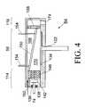
- Process chamber 54includes preprocess zone 114 , process zone 58 , and postprocess zone 118 .
- Gas inject conduit 74is connected with preprocess zone 114 so as to provide process gas to process chamber 54 .
- process chamber 54has a hole 136 through which gas inject conduit 74 passes into process chamber 54 .
- a seal bushing 138forms a seal around gas inject conduit 74 so as to restrict process gas loss from process chamber 54 .
- sealed bushing 138does not form a gas tight seal so that seal bushing 138 can allow gas leakage between process chamber 54 and housing 30 .
- gas inject conduit 74includes a gas dispersion head 142 having holes for dispersing process gas in preprocess zone 114 of process chamber 54 .
- a process gas preheater 146is located between gas dispersion head 142 and process zone 58 so that process gases entering preprocess zone 114 pass through gas preheater 146 before entering process zone 58 .
- Gas preheater 146facilitates heating the process gas to the preprocess temperature.
- Gas preheater 146includes a body of a thermally refractory material such as silicon carbide, silicon carbide coated graphite, quartz, and ceramics.
- Gas preheater 146has a plurality of holes for allowing the process gas to pass therethrough. In a preferred embodiment, the holes in gas preheater 146 are arranged to distribute the process gas so that the process gas is urged to maintain laminar flow upon exit from gas preheater 146 .
- Process zone 58has recessed area 134 in the bottom surface of process chamber 54 .
- Wafer support 122is positioned in process zone 58 .
- Wafer support 122has disk 126 for contacting the wafer.
- disk 126is arranged to fit into recessed area 134 so that the top surface of the wafer can be held substantially planar with respect to the areas of the bottom surface of process zone 58 that surround recessed area 134 .
- Wafer support 122is arranged so as to allow rotation of the wafer during processing.
- wafer support 122is coupled with process chamber 54 so as to allow rotation of the wafer support.
- a motor(not shown in FIG. 4) is rotatably coupled to wafer support 122 so as to cause rotation of wafer support 122 .
- a velocity gradient plate 150is connected with process chamber 54 .
- velocity gradient plate 150is substantially rigid and is substantially inert to the process gas.
- Velocity gradient plate 150is arranged adjacent to the wafer support so as to define one side of a channel for process gas flow over the wafer holding surface of wafer support 122 , such that the cross-sectional area for the channel decreases in the direction of the process gas flow in response to perpendicular distance variations between velocity gradient plate 150 and the wafer holding surface of wafer support 122 .
- velocity gradient plate 150includes a refractory material. Examples of materials that can be used in velocity gradient plate 150 include materials such as quartz, silicon carbide, silicon carbide coated graphite, and ceramics.
- velocity gradient plate 150is movably connected with process chamber 54 so that the distance between velocity gradient plate 150 and wafer support 122 can be adjusted as another process parameter.
- the distance between velocity gradient plate 150 and wafer support 122can be adjusted and the angle between velocity gradient plate 150 and wafer support 122 can be adjusted.
- velocity gradient plate connector 154suspends velocity gradient plate 150 from the top of process chamber 54 .
- the length of connector 154can be varied so as to change the position of velocity gradient plate 150 with respect to wafer support 122 .
- Velocity gradient plate 150causes the process gas to have improved mass transfer characteristics as the process gas flows over the wafer.
- the improved mass transfer characteristicshelp to compensate for depletion of reactants in the process gas.
- the reduction of depletionaffects improves uniformity of deposited layer properties such as thickness uniformity, composition, optical properties, and electrical properties.
- Velocity gradient plate 150is positioned adjacent to gas preheater 146 so that process gas exiting gas preheater 146 is influenced by velocity gradient plate 150 as the gas passes through process zone 58 .
- velocity gradient plate 150may include holes (not shown in FIG. 4) to allow viewing the wafer using optical fibers without obstructions caused by velocity gradient plate 150 .
- the holesare sized so as to leave the process gas flow through process zone 58 substantially unaffected.
- velocity gradient plate 150has an inverted “U” shape for improved confinement of process gas flow above the wafer.
- opposite edges of velocity gradient plate 150are directed downward so that velocity gradient plate 150 defines at least part of the sidewalls of the channel for gas flow above the wafer.
- An exhaust baffle plate 158separates process zone 58 from postprocess zone 118 .
- Baffle plate 158has at least one hole to allow gas flow from process zone 58 into postprocess zone 118 .
- One function of baffle plate 158is to help to reduce back circulation of gases from postprocess zone 118 back into process zone 58 .
- preprocess zone 114includes a process chamber purge gas injector 162 for providing a purge gas such as hydrogen or an inert gas to process chamber 54 .
- purge gas injector 162is configured to flow purge gas from preprocess zone 114 through volume 166 of process zone 58 .
- Volume 166substantially excludes volume 170 , located between velocity gradient plate 150 and wafer support 122 .
- One function of the purge flowis to help confine the process gas flow to volume 170 so as to maximize the process gas exposure to the wafer.
- the process chamber purge gas flowis particularly important for embodiments in which velocity gradient plate 150 has holes for temperature measurement.
- the purge gas flowexits process chamber 54 via postprocess zone 118 .
- Exhaust baffle plate 158has at least one hole for conveying the purge gas from process zone 58 to postprocess zone 118 .
- Postprocess zone 118has a hole 174 for exhaust gas and purge gas to exit process chamber 54 .
- Gas injector 178includes three sections: process gas sections 182 a and 182 b for carrying process gas and a purge gas section 186 for carrying purge gas.
- Each sectionhas a plurality of holes 189 .
- the holesare substantially parallel within a section. The holes distribute the process gas so that the direction of the gas flow is substantially parallel to the plane of the wafer holder. In other words, a showerhead type of gas flow is directed approximately parallel to the wafer surface.
- gas injector 178is arranged so that the gases can be selectively distributed across the wafer independently or together so as to obtain improved process uniformity control. Improved uniformity is obtainable by selectively distributing the gas across the wafer to compensate for variations in reaction rate caused by thermal gradients and gas flow.
- the vertical showerhead configurationenables high growth rates, typical of showerheads, while avoiding problems with particulates that are common for some of the conventional showerheads. For example, the vertical showerhead is less likely to have particles fall from the showerhead onto the wafer surface.
- Embodiments of the present invention, for deposition applicationsinclude showerhead materials having good adhesion properties for the material being deposited. Referring now to FIG. 6 wherein there is shown an example configuration for heat shields 190 .
- Heat shields 190include a first heat shield 190 a and a second heat shield 190 b . Heat shield 190 a and heat shield 190 b are positioned to provide heat shielding for the same areas of process chamber 54 .
- a spaceis maintained between the heat shields.
- physical contact between the heat shieldsis held at a minimum.
- the space between the heat shieldsis maintained by placing one or more spacers 194 between the heat shields.
- Suitable materials for spacers 194include thermally refractory materials such as quartz, polysilicon, silicon carbide, silicon carbide coated graphite, and ceramics.
- spacers 194are shaped like balls having diameters about equal to the desired spacing to be maintained between the heat shields.
- Spacers 194can also be used to maintain desired spaces between other components of the apparatus such as heating elements 66 , strip heaters 110 , and process chamber 54 . As shown in FIG. 6, spacer 194 is used to maintain a space between heat shield 190 b and an outer surface of process chamber 54 . The strip heater 110 is shown sandwiched between heat shield 190 b and process chamber 54 .
- the heat shieldshave surface structures that produce substantially the same result achieved using the spacers just described.
- the heat shieldscan have protrusions from the surface of the heat shield so that the protrusions substantially maintain the desired spacing between adjacent heat shields or other adjacent surfaces.
- a single heat shieldmay be used or multiple heat shields may be used for heat shielding the same area.
- Wafer support 122including disk 126 and wafer holder stem 130 .
- Wafer holder stem 130is attached substantially at the center of disk 126 so that wafer support 122 can rotate about the axis of wafer holder stem 130 to rotate the wafer.
- Wafer holder stem 130extends through process chamber 54 (not shown in FIG. 7 ); wafer support 122 is connected with process chamber 54 to allow rotation of wafer support 122 .
- Wafer holder stem 130extends through the bottom surface of housing 30 ; wafer holder stem 130 is connected with the bottom of housing 30 to allow rotation of wafer support 122 .
- Wafer holder stem 130is rotatably coupled to a motor 198 for rotating wafer support 122 .
- a linear actuator 202is connected with motor 198 ; linear actuator 202 is capable of lifting and lowering motor 198 .
- Motor 198is coupled to wafer holder stem 130 so that lifting and lowering of motor 198 by linear actuator 202 causes wafer holder 122 to be lifted and lowered.
- Lifting and lowering wafer support 122can be used to facilitate loading and unloading wafers to and from wafer support 122 .
- a rotary feedthrough 206such as a standard commercially available rotary feed through is connected between motor 198 and wafer holder stem 130 so as to transfer rotary motion and up-and-down motion.
- a bellows 210is connected to the bottom of housing 30 at one end of bellows 210 .
- Bellows 210surrounds wafer holder stem 130 .
- a mounting plate 214is attached to the other end of bellows 210 .
- the attachments to bellows 210are substantially gas tight.
- Rotary feed through 206is attached to mounting plate 214 so as to enable rotation of wafer support 122 by motor 198 .
- Bellows 210is configured so as to allow up and down motion of motor 198 for lifting and lowering wafer support 122 .
- wafer holder stem 130has a bore such as axial bore 218 .
- Disk 126has a hole 222 corresponding to axial bore 218 .
- Wafer holder stem 130is configured to have a vacuum source apply a vacuum to axial bore 218 so that a low pressure is generated at hole 222 .
- the low-pressure generated at hole 222is sufficient to enable disk 126 to a function as a vacuum chuck for holding the wafer on wafer support 122 .
- An advantage of embodiments of the present inventiondue to the process chamber materials and hot wall operation, is the removal of the conventional growth rate restrictions for applications such as silicon epitaxy.
- Embodiments of the present inventioncan allow epitaxial silicon growth with high intrinsic resistivity values at substantially higher growth rates and higher temperatures without wall deposit problems. Furthermore, the advantages of no pattern shift, no distortion, and no washout with patterned wafers are maintained using a non-chlorinated silicon source.
- embodiments of the present inventioncan be used or a wide variety of elevated temperature processes for semiconductor device fabrication. Changes in the selected process gases allow embodiments of the present invention to be suitable for semiconductor wafer processing steps such as annealing, activating dopant, depositing by chemical vapor deposition, depositing by epitaxial deposition, doping, forming a silicide, nitriding, oxidizing, reflowing a deposit, and recrystallizing.
Landscapes
- Engineering & Computer Science (AREA)
- Microelectronics & Electronic Packaging (AREA)
- Condensed Matter Physics & Semiconductors (AREA)
- General Physics & Mathematics (AREA)
- Manufacturing & Machinery (AREA)
- Computer Hardware Design (AREA)
- Physics & Mathematics (AREA)
- Power Engineering (AREA)
- Chemical Vapour Deposition (AREA)
- Crystals, And After-Treatments Of Crystals (AREA)
- Exposure Of Semiconductors, Excluding Electron Or Ion Beam Exposure (AREA)
- Drying Of Semiconductors (AREA)
- Physical Vapour Deposition (AREA)
Abstract
Description
Claims (30)
Priority Applications (12)
| Application Number | Priority Date | Filing Date | Title |
|---|---|---|---|
| US09/550,888US6331212B1 (en) | 2000-04-17 | 2000-04-17 | Methods and apparatus for thermally processing wafers |
| CNB018098576ACN1199236C (en) | 2000-04-17 | 2001-04-12 | Method and apparatus for heat treatment of wafer |
| KR1020027013933AKR100793329B1 (en) | 2000-04-17 | 2001-04-12 | Methods and apparatus for heat treating wafers |
| DE60133376TDE60133376T2 (en) | 2000-04-17 | 2001-04-12 | DEVICE FOR THE THERMAL PROCESSING OF WAFERS |
| HK03109446.8AHK1057130B (en) | 2000-04-17 | 2001-04-12 | Methods and apparatus for thermally processing wafers |
| JP2001577590AJP2003531489A (en) | 2000-04-17 | 2001-04-12 | Method and apparatus for heat treating a wafer |
| PCT/US2001/040511WO2001080291A1 (en) | 2000-04-17 | 2001-04-12 | Methods and apparatus for thermally processing wafers |
| AU2001253890AAU2001253890A1 (en) | 2000-04-17 | 2001-04-12 | Methods and apparatus for thermally processing wafers |
| AT01927443TATE390705T1 (en) | 2000-04-17 | 2001-04-12 | DEVICE FOR THERMAL PROCESSING OF WAFERS |
| EP01927443AEP1275135B1 (en) | 2000-04-17 | 2001-04-12 | Apparatus for thermally processing wafers |
| TW090109009ATW529059B (en) | 2000-04-17 | 2001-04-16 | Method and apparatus for thermally processing wafers |
| US09/900,594US6774060B2 (en) | 2000-04-17 | 2001-07-07 | Methods and apparatus for thermally processing wafers |
Applications Claiming Priority (1)
| Application Number | Priority Date | Filing Date | Title |
|---|---|---|---|
| US09/550,888US6331212B1 (en) | 2000-04-17 | 2000-04-17 | Methods and apparatus for thermally processing wafers |
Related Child Applications (1)
| Application Number | Title | Priority Date | Filing Date |
|---|---|---|---|
| US09/900,594DivisionUS6774060B2 (en) | 2000-04-17 | 2001-07-07 | Methods and apparatus for thermally processing wafers |
Publications (1)
| Publication Number | Publication Date |
|---|---|
| US6331212B1true US6331212B1 (en) | 2001-12-18 |
Family
ID=24198985
Family Applications (2)
| Application Number | Title | Priority Date | Filing Date |
|---|---|---|---|
| US09/550,888Expired - Fee RelatedUS6331212B1 (en) | 2000-04-17 | 2000-04-17 | Methods and apparatus for thermally processing wafers |
| US09/900,594Expired - Fee RelatedUS6774060B2 (en) | 2000-04-17 | 2001-07-07 | Methods and apparatus for thermally processing wafers |
Family Applications After (1)
| Application Number | Title | Priority Date | Filing Date |
|---|---|---|---|
| US09/900,594Expired - Fee RelatedUS6774060B2 (en) | 2000-04-17 | 2001-07-07 | Methods and apparatus for thermally processing wafers |
Country Status (10)
| Country | Link |
|---|---|
| US (2) | US6331212B1 (en) |
| EP (1) | EP1275135B1 (en) |
| JP (1) | JP2003531489A (en) |
| KR (1) | KR100793329B1 (en) |
| CN (1) | CN1199236C (en) |
| AT (1) | ATE390705T1 (en) |
| AU (1) | AU2001253890A1 (en) |
| DE (1) | DE60133376T2 (en) |
| TW (1) | TW529059B (en) |
| WO (1) | WO2001080291A1 (en) |
Cited By (48)
| Publication number | Priority date | Publication date | Assignee | Title |
|---|---|---|---|---|
| US20020056417A1 (en)* | 2000-11-14 | 2002-05-16 | Tokyo Electron Limited | Substrate processing apparatus and substrate processing method |
| US6442950B1 (en)* | 2001-05-23 | 2002-09-03 | Macronix International Co., Ltd. | Cooling system of chamber with removable liner |
| US20020129768A1 (en)* | 2001-03-15 | 2002-09-19 | Carpenter Craig M. | Chemical vapor deposition apparatuses and deposition methods |
| US20030036877A1 (en)* | 2001-07-23 | 2003-02-20 | Schietinger Charles W. | In-situ wafer parameter measurement method employing a hot susceptor as a reflected light source |
| US20030197155A1 (en)* | 2001-07-16 | 2003-10-23 | Nec Corporation | Mercury-containing copper oxide superconductor film, manufacturing apparatus thereof and manufacturing process thereof |
| US20040035360A1 (en)* | 2002-05-17 | 2004-02-26 | Semiconductor Energy Laboratory Co., Ltd. | Manufacturing apparatus |
| US6709267B1 (en) | 2002-12-27 | 2004-03-23 | Asm America, Inc. | Substrate holder with deep annular groove to prevent edge heat loss |
| US20040071874A1 (en)* | 2002-04-12 | 2004-04-15 | Asm Japan K.K. | Apparatus and method for single-wafer-processing type CVD |
| US20040149210A1 (en)* | 2001-05-17 | 2004-08-05 | Fink Steven T | Cylinder-based plasma processing system |
| US20040169032A1 (en)* | 2003-02-27 | 2004-09-02 | Dainippon Screen Mfg. Co., Ltd. | Heat treatment apparatus by means of light irradiation |
| US20040255442A1 (en)* | 2003-06-19 | 2004-12-23 | Mcdiarmid James | Methods and apparatus for processing workpieces |
| US6896738B2 (en)* | 2001-10-30 | 2005-05-24 | Cree, Inc. | Induction heating devices and methods for controllably heating an article |
| US20050111161A1 (en)* | 2003-11-25 | 2005-05-26 | Daniel Tran | Compact pinlifter assembly integrated in wafer chuck |
| US20050133159A1 (en)* | 2001-04-12 | 2005-06-23 | Johnsgard Kristian E. | Systems and methods for epitaxially depositing films on a semiconductor substrate |
| US20050193947A1 (en)* | 2002-08-15 | 2005-09-08 | Cem Basceri | Deposition reactors and systems |
| US20060021578A1 (en)* | 2004-07-28 | 2006-02-02 | Jung-Hun Seo | Chemical vapor deposition apparatus |
| US20060190211A1 (en)* | 2001-07-23 | 2006-08-24 | Schietinger Charles W | In-situ wafer parameter measurement method employing a hot susceptor as radiation source for reflectance measurement |
| WO2005124859A3 (en)* | 2004-06-10 | 2006-10-05 | Avansys Inc | Methods and apparatuses for depositing uniform layers |
| US20070084408A1 (en)* | 2005-10-13 | 2007-04-19 | Applied Materials, Inc. | Batch processing chamber with diffuser plate and injector assembly |
| US20070084406A1 (en)* | 2005-10-13 | 2007-04-19 | Joseph Yudovsky | Reaction chamber with opposing pockets for gas injection and exhaust |
| US20070099411A1 (en)* | 2005-11-02 | 2007-05-03 | Fujitsu Limited | Reflow apparatus, a reflow method, and a manufacturing method of semiconductor device |
| US20090197402A1 (en)* | 2008-01-31 | 2009-08-06 | Hitachi Kokusai Electric, Inc. | Substrate processing apparatus, method for manufacturing semiconductor device, and process tube |
| US20090226293A1 (en)* | 2005-07-06 | 2009-09-10 | Sumco Techxiv Kabushiki Kaisha | Method and Apparatus for Manufacturing Semiconductor Wafer |
| US20090269486A1 (en)* | 2002-05-17 | 2009-10-29 | Semiconductor Energy Laboratory Co., Ltd. | Evaporation method, evaporation device and method of fabricating light emitting device |
| US20090325116A1 (en)* | 2007-08-10 | 2009-12-31 | Toyota Jidosha Kabushiki Kaisha | Heating furnace and heating method employed by heating furnace |
| US20100015359A1 (en)* | 2006-12-25 | 2010-01-21 | Tokyo Electron Limited | Film deposition apparatus and method |
| WO2010005620A3 (en)* | 2008-06-30 | 2010-03-04 | S.O.I.Tec Silicon On Insulator Technologies | Modular and readily configurable reactor enclosures and associated function modules |
| US20100101495A1 (en)* | 2004-11-15 | 2010-04-29 | Cree, Inc. | Restricted Radiated Heating Assembly for High Temperature Processing |
| US20100112216A1 (en)* | 2008-11-06 | 2010-05-06 | Veeco Instruments Inc. | Chemical vapor deposition with elevated temperature gas injection |
| US20100199914A1 (en)* | 2007-10-10 | 2010-08-12 | Michael Iza | Chemical vapor deposition reactor chamber |
| KR101001314B1 (en) | 2008-11-17 | 2010-12-14 | 세메스 주식회사 | Substrate processing apparatus |
| US20110073039A1 (en)* | 2009-09-28 | 2011-03-31 | Ron Colvin | Semiconductor deposition system and method |
| US20110100973A1 (en)* | 2009-10-29 | 2011-05-05 | Samsung Mobile Display Co., Ltd. | Apparatus for thermally processing substrate |
| US20110210118A1 (en)* | 2010-02-26 | 2011-09-01 | Hitachi Kokusai Electric Inc. | Substrate processing apparatus, method of manufacturing semiconductor device and method of manufacturing substrate |
| US20120181265A1 (en)* | 2010-07-15 | 2012-07-19 | Despatch Industries Limited Partnership | Firing furnace configuration for thermal processing system |
| US20140345526A1 (en)* | 2013-05-23 | 2014-11-27 | Applied Materials, Inc. | Coated liner assembly for a semiconductor processing chamber |
| WO2013005155A3 (en)* | 2011-07-07 | 2015-08-06 | Lam Research Ag | Apparatus for treating a wafer-shaped article |
| US20160160349A1 (en)* | 2014-12-04 | 2016-06-09 | Seong-Joon CHO | Chemical vapor deposition apparatus and method of manufacturing light-emitting diode device using the same |
| US9382642B2 (en) | 2009-04-17 | 2016-07-05 | Lpe S.P.A. | Reaction chamber of an epitaxial reactor and reactor that uses said chamber |
| US9799517B2 (en) | 2015-07-06 | 2017-10-24 | SCREEN Holdings Co., Ltd. | Apparatus and method for light-irradiation heat treatment |
| US9808891B2 (en)* | 2014-01-16 | 2017-11-07 | Taiwan Semiconductor Manufacturing Co., Ltd. | Tool and method of reflow |
| US9947562B2 (en) | 2005-08-05 | 2018-04-17 | Applied Materials, Inc. | Method and apparatus for processing semiconductor work pieces |
| US20180261480A1 (en)* | 2017-03-10 | 2018-09-13 | Applied Materials, Inc. | High pressure wafer processing systems and related methods |
| US10138551B2 (en) | 2010-07-29 | 2018-11-27 | GES Associates LLC | Substrate processing apparatuses and systems |
| US20190119769A1 (en)* | 2017-07-14 | 2019-04-25 | Micromaterials, LLC. | Gas delivery system for high pressure processing chamber |
| US11032945B2 (en)* | 2019-07-12 | 2021-06-08 | Applied Materials, Inc. | Heat shield assembly for an epitaxy chamber |
| US11208724B2 (en)* | 2017-05-09 | 2021-12-28 | Tokyo Electron Limited | Film forming apparatus |
| US20220275505A1 (en)* | 2021-02-26 | 2022-09-01 | Applied Materials, Inc. | High throughput and metal contamination control oven for chamber component cleaning process |
Families Citing this family (33)
| Publication number | Priority date | Publication date | Assignee | Title |
|---|---|---|---|---|
| JP3607664B2 (en)* | 2000-12-12 | 2005-01-05 | 日本碍子株式会社 | III-V nitride film manufacturing apparatus |
| US6861321B2 (en)* | 2002-04-05 | 2005-03-01 | Asm America, Inc. | Method of loading a wafer onto a wafer holder to reduce thermal shock |
| DE10303700B4 (en) | 2003-01-30 | 2005-09-22 | Siemens Ag | Method for interference suppression |
| US20040182315A1 (en)* | 2003-03-17 | 2004-09-23 | Tokyo Electron Limited | Reduced maintenance chemical oxide removal (COR) processing system |
| US6951821B2 (en)* | 2003-03-17 | 2005-10-04 | Tokyo Electron Limited | Processing system and method for chemically treating a substrate |
| CN1301534C (en)* | 2003-07-15 | 2007-02-21 | 旺宏电子股份有限公司 | Prevention methods for abnormal events of semiconductor furnace tube temperature and gas flow |
| CN1307686C (en)* | 2003-10-14 | 2007-03-28 | 茂德科技股份有限公司 | Batch processing device and wafer processing method |
| CN100530523C (en)* | 2003-10-27 | 2009-08-19 | 应用材料股份有限公司 | Method of Correcting Temperature Uniformity |
| US7105840B2 (en)* | 2005-02-03 | 2006-09-12 | Axcelis Technologies, Inc. | Ion source for use in an ion implanter |
| US7691208B2 (en)* | 2005-08-31 | 2010-04-06 | Tokyo Electron Limited | Cleaning method |
| US7732009B2 (en)* | 2006-09-26 | 2010-06-08 | United Microelectronics Corp. | Method of cleaning reaction chamber, method of forming protection film and protection wafer |
| DE112009000929T5 (en)* | 2008-04-17 | 2013-10-10 | Honda Motor Co., Ltd. | Heat treatment device for solar cells |
| DE102010009795B4 (en)* | 2010-03-01 | 2014-05-15 | Von Ardenne Anlagentechnik Gmbh | Method and device for producing metal back contacts for wafer-based solar cells |
| CN102465335B (en)* | 2010-11-18 | 2014-07-16 | 南京大学 | Heating device for semiconducting material hot wall epitaxy growth system |
| CN102634850A (en)* | 2012-03-31 | 2012-08-15 | 江苏鑫和泰光电科技有限公司 | Annealing method of sapphire wafer |
| US20150165475A1 (en)* | 2012-07-09 | 2015-06-18 | Saint-Gobain Glass France | Process box, assembly, and method for processing a coated substrate |
| JP5933837B2 (en)* | 2012-07-09 | 2016-06-15 | サン−ゴバン グラス フランスSaint−Gobain Glass France | System and method for processing a substrate |
| JP6116685B2 (en)* | 2012-07-09 | 2017-04-19 | サン−ゴバン グラス フランスSaint−Gobain Glass France | Apparatus and method for heat treating an object |
| CN103866282B (en)* | 2012-12-14 | 2016-12-21 | 北京北方微电子基地设备工艺研究中心有限责任公司 | Pecvd device |
| TWI470105B (en)* | 2013-06-03 | 2015-01-21 | Adpv Technology Ltd | Gas Reaction Continuous Cavity and Gas Reaction |
| US9087864B2 (en)* | 2013-12-19 | 2015-07-21 | Intermolecular, Inc. | Multipurpose combinatorial vapor phase deposition chamber |
| US20160002775A1 (en)* | 2014-07-02 | 2016-01-07 | Rolls-Royce Corporation | Multilayer liner for chemical vapor deposition furnace |
| KR101651880B1 (en)* | 2014-10-13 | 2016-08-29 | 주식회사 테스 | Apparatus for mocvd |
| US9982364B2 (en) | 2015-04-07 | 2018-05-29 | Applied Materials, Inc. | Process gas preheating systems and methods for double-sided multi-substrate batch processing |
| JP6707827B2 (en)* | 2015-09-28 | 2020-06-10 | 東京エレクトロン株式会社 | Film forming equipment |
| CN107435164A (en)* | 2016-05-25 | 2017-12-05 | 上海新昇半导体科技有限公司 | Epitaxial growth equipment |
| CN115468626A (en)* | 2017-07-27 | 2022-12-13 | 沃特洛电气制造公司 | Sensor system and integrated heater-sensor for measuring and controlling heater system performance |
| GB201815815D0 (en)* | 2018-09-28 | 2018-11-14 | Metryx Ltd | Method and apparatus for controlling the temperature of a semiconductor wafer |
| JP7257813B2 (en)* | 2019-02-21 | 2023-04-14 | 東京エレクトロン株式会社 | Steam treatment device and steam treatment method |
| SE543143C2 (en) | 2019-04-12 | 2020-10-13 | Epiluvac Ab | Device and method for ensuring flatness of wafer during growth |
| CN110512287A (en)* | 2019-09-12 | 2019-11-29 | 江苏吉星新材料有限公司 | A kind of 4 inch sapphire crystal method for annealing |
| KR102564228B1 (en)* | 2021-04-29 | 2023-08-09 | 주식회사 테스 | Metal organic chemical vapor deposition apparatus |
| US20240254654A1 (en)* | 2023-01-26 | 2024-08-01 | Applied Materials, Inc. | Epi isolation plate with gap and angle adjustment for process tuning |
Citations (37)
| Publication number | Priority date | Publication date | Assignee | Title |
|---|---|---|---|---|
| US3603284A (en)* | 1970-01-02 | 1971-09-07 | Ibm | Vapor deposition apparatus |
| US3862397A (en)* | 1972-03-24 | 1975-01-21 | Applied Materials Tech | Cool wall radiantly heated reactor |
| US4081313A (en) | 1975-01-24 | 1978-03-28 | Applied Materials, Inc. | Process for preparing semiconductor wafers with substantially no crystallographic slip |
| US4167915A (en)* | 1977-03-09 | 1979-09-18 | Atomel Corporation | High-pressure, high-temperature gaseous chemical apparatus |
| US4347431A (en)* | 1980-07-25 | 1982-08-31 | Bell Telephone Laboratories, Inc. | Diffusion furnace |
| US4481406A (en)* | 1983-01-21 | 1984-11-06 | Varian Associates, Inc. | Heater assembly for thermal processing of a semiconductor wafer in a vacuum chamber |
| US4496609A (en) | 1969-10-15 | 1985-01-29 | Applied Materials, Inc. | Chemical vapor deposition coating process employing radiant heat and a susceptor |
| US4558660A (en)* | 1982-03-16 | 1985-12-17 | Handotai Kenkyu Shinkokai | Semiconductor fabricating apparatus |
| US4651673A (en)* | 1982-09-02 | 1987-03-24 | At&T Technologies, Inc. | CVD apparatus |
| US4728389A (en) | 1985-05-20 | 1988-03-01 | Applied Materials, Inc. | Particulate-free epitaxial process |
| US4753192A (en)* | 1987-01-08 | 1988-06-28 | Btu Engineering Corporation | Movable core fast cool-down furnace |
| US4836138A (en) | 1987-06-18 | 1989-06-06 | Epsilon Technology, Inc. | Heating system for reaction chamber of chemical vapor deposition equipment |
| US4849608A (en)* | 1987-02-14 | 1989-07-18 | Dainippon Screen Mfg. Co., Ltd. | Apparatus for heat-treating wafers |
| US4886954A (en)* | 1988-04-15 | 1989-12-12 | Thermco Systems, Inc. | Hot wall diffusion furnace and method for operating the furnace |
| US4975561A (en) | 1987-06-18 | 1990-12-04 | Epsilon Technology Inc. | Heating system for substrates |
| US4976996A (en) | 1987-02-17 | 1990-12-11 | Lam Research Corporation | Chemical vapor deposition reactor and method of use thereof |
| US5128515A (en)* | 1990-05-21 | 1992-07-07 | Tokyo Electron Sagami Limited | Heating apparatus |
| US5154512A (en)* | 1990-04-10 | 1992-10-13 | Luxtron Corporation | Non-contact techniques for measuring temperature or radiation-heated objects |
| US5305416A (en)* | 1993-04-02 | 1994-04-19 | At&T Bell Laboratories | Semiconductor processing technique, including pyrometric measurement of radiantly heated bodies |
| US5324920A (en)* | 1990-10-18 | 1994-06-28 | Tokyo Electron Sagami Limited | Heat treatment apparatus |
| US5332557A (en)* | 1992-01-22 | 1994-07-26 | Tokyo Ohka Kogyo Co., Ltd. | Heating apparatus |
| US5482559A (en)* | 1993-10-21 | 1996-01-09 | Tokyo Electron Kabushiki Kaisha | Heat treatment boat |
| US5536919A (en)* | 1994-11-22 | 1996-07-16 | Taheri; Ramtin | Heating chamber |
| US5603772A (en)* | 1994-08-16 | 1997-02-18 | Nec Corporation | Furnace equipped with independently controllable heater elements for uniformly heating semiconductor wafers |
| US5622639A (en)* | 1993-07-29 | 1997-04-22 | Tokyo Electron Kabushiki Kaisha | Heat treating apparatus |
| US5624590A (en)* | 1993-04-02 | 1997-04-29 | Lucent Technologies, Inc. | Semiconductor processing technique, including pyrometric measurement of radiantly heated bodies and an apparatus for practicing this technique |
| US5636320A (en)* | 1995-05-26 | 1997-06-03 | International Business Machines Corporation | Sealed chamber with heating lamps provided within transparent tubes |
| US5800616A (en)* | 1997-12-15 | 1998-09-01 | Sony Corporation | Vertical LPCVD furnace with reversible manifold collar and method of retrofitting same |
| US5861609A (en)* | 1995-10-02 | 1999-01-19 | Kaltenbrunner; Guenter | Method and apparatus for rapid thermal processing |
| US5891251A (en) | 1996-08-07 | 1999-04-06 | Macleish; Joseph H. | CVD reactor having heated process chamber within isolation chamber |
| US5902406A (en)* | 1996-03-15 | 1999-05-11 | Asahi Glass Company Ltd. | Low pressure CVD system |
| US6021152A (en)* | 1997-07-11 | 2000-02-01 | Asm America, Inc. | Reflective surface for CVD reactor walls |
| US6063199A (en)* | 1997-09-11 | 2000-05-16 | Applied Materials, Inc. | Temperature controlled liner |
| US6075922A (en)* | 1997-08-07 | 2000-06-13 | Steag Rtp Systems, Inc. | Process for preventing gas leaks in an atmospheric thermal processing chamber |
| US6093253A (en)* | 1998-04-06 | 2000-07-25 | Abb Research Ltd. | Method and a device for epitaxial growth of objects by chemical vapor deposition |
| US6191392B1 (en)* | 1997-12-08 | 2001-02-20 | Steag Ast Elektronik Gmbh | Method of measuring electromagnetic radiation |
| US6246031B1 (en)* | 1999-11-30 | 2001-06-12 | Wafermasters, Inc. | Mini batch furnace |
Family Cites Families (21)
| Publication number | Priority date | Publication date | Assignee | Title |
|---|---|---|---|---|
| US685906A (en)* | 1901-03-21 | 1901-11-05 | Eugene Brown | Combined milk dipper and measure. |
| JPS5632400A (en)* | 1979-08-16 | 1981-04-01 | Toshiba Corp | Vapor phase growing method for gallium phosphide layer |
| JPS60112694A (en)* | 1983-11-21 | 1985-06-19 | Matsushita Electric Ind Co Ltd | Gas-phase growth method of compound semiconductor |
| JPH03116929A (en)* | 1989-09-29 | 1991-05-17 | Nec Yamaguchi Ltd | Heat treatment device for semiconductor substrate |
| JP2551172B2 (en)* | 1989-11-29 | 1996-11-06 | 富士通株式会社 | Vapor phase epitaxial growth system |
| JPH04349623A (en)* | 1991-05-28 | 1992-12-04 | Fuji Electric Co Ltd | Vapor phase growth equipment |
| US5431958A (en)* | 1992-03-09 | 1995-07-11 | Sharp Kabushiki Kaisha | Metalorganic chemical vapor deposition of ferroelectric thin films |
| US5440101A (en)* | 1993-04-19 | 1995-08-08 | Research, Incorporated | Continuous oven with a plurality of heating zones |
| JPH07283155A (en)* | 1994-04-01 | 1995-10-27 | Kokusai Electric Co Ltd | Semiconductor manufacturing equipment |
| JPH08330317A (en)* | 1995-05-31 | 1996-12-13 | F T L:Kk | Method for manufacturing semiconductor device |
| JPH09106950A (en)* | 1995-10-12 | 1997-04-22 | Nec Corp | Crystal growth apparatus and crystal processing apparatus |
| US5854468A (en)* | 1996-01-25 | 1998-12-29 | Brooks Automation, Inc. | Substrate heating apparatus with cantilevered lifting arm |
| JPH1092754A (en)* | 1996-09-18 | 1998-04-10 | Tokyo Electron Ltd | Method and device for single wafer heat treatment |
| KR100443415B1 (en)* | 1996-02-23 | 2004-11-03 | 동경 엘렉트론 주식회사 | Heat treatment device |
| US6133550A (en)* | 1996-03-22 | 2000-10-17 | Sandia Corporation | Method and apparatus for thermal processing of semiconductor substrates |
| TW336333B (en) | 1996-06-24 | 1998-07-11 | Nat Denki Kk | A substrate processing apparatus |
| JP3200396B2 (en)* | 1996-06-24 | 2001-08-20 | 株式会社日立国際電気 | Substrate processing apparatus and film forming method |
| ES2216104T3 (en)* | 1997-04-22 | 2004-10-16 | Imec Vzw | OVEN FOR CONTINUOUS HIGH PERFORMANCE DISSEMINATION PROCESSES WITH VARIOUS SOURCES OF DIFFUSION. |
| US5911896A (en)* | 1997-06-25 | 1999-06-15 | Brooks Automation, Inc. | Substrate heating apparatus with glass-ceramic panels and thin film ribbon heater element |
| JPH1174202A (en)* | 1997-08-29 | 1999-03-16 | Sharp Corp | Gallium nitride III-V compound semiconductor vapor phase growth apparatus, gallium nitride III-V compound semiconductor device, and method of manufacturing the same |
| JP3068075B2 (en)* | 1998-01-17 | 2000-07-24 | ハンベック コーポレイション | Horizontal reactor for compound semiconductor production |
- 2000
- 2000-04-17USUS09/550,888patent/US6331212B1/ennot_activeExpired - Fee Related
- 2001
- 2001-04-12CNCNB018098576Apatent/CN1199236C/ennot_activeExpired - Fee Related
- 2001-04-12EPEP01927443Apatent/EP1275135B1/ennot_activeExpired - Lifetime
- 2001-04-12ATAT01927443Tpatent/ATE390705T1/ennot_activeIP Right Cessation
- 2001-04-12JPJP2001577590Apatent/JP2003531489A/enactivePending
- 2001-04-12DEDE60133376Tpatent/DE60133376T2/ennot_activeExpired - Lifetime
- 2001-04-12AUAU2001253890Apatent/AU2001253890A1/ennot_activeAbandoned
- 2001-04-12WOPCT/US2001/040511patent/WO2001080291A1/enactiveApplication Filing
- 2001-04-12KRKR1020027013933Apatent/KR100793329B1/ennot_activeExpired - Fee Related
- 2001-04-16TWTW090109009Apatent/TW529059B/ennot_activeIP Right Cessation
- 2001-07-07USUS09/900,594patent/US6774060B2/ennot_activeExpired - Fee Related
Patent Citations (37)
| Publication number | Priority date | Publication date | Assignee | Title |
|---|---|---|---|---|
| US4496609A (en) | 1969-10-15 | 1985-01-29 | Applied Materials, Inc. | Chemical vapor deposition coating process employing radiant heat and a susceptor |
| US3603284A (en)* | 1970-01-02 | 1971-09-07 | Ibm | Vapor deposition apparatus |
| US3862397A (en)* | 1972-03-24 | 1975-01-21 | Applied Materials Tech | Cool wall radiantly heated reactor |
| US4081313A (en) | 1975-01-24 | 1978-03-28 | Applied Materials, Inc. | Process for preparing semiconductor wafers with substantially no crystallographic slip |
| US4167915A (en)* | 1977-03-09 | 1979-09-18 | Atomel Corporation | High-pressure, high-temperature gaseous chemical apparatus |
| US4347431A (en)* | 1980-07-25 | 1982-08-31 | Bell Telephone Laboratories, Inc. | Diffusion furnace |
| US4558660A (en)* | 1982-03-16 | 1985-12-17 | Handotai Kenkyu Shinkokai | Semiconductor fabricating apparatus |
| US4651673A (en)* | 1982-09-02 | 1987-03-24 | At&T Technologies, Inc. | CVD apparatus |
| US4481406A (en)* | 1983-01-21 | 1984-11-06 | Varian Associates, Inc. | Heater assembly for thermal processing of a semiconductor wafer in a vacuum chamber |
| US4728389A (en) | 1985-05-20 | 1988-03-01 | Applied Materials, Inc. | Particulate-free epitaxial process |
| US4753192A (en)* | 1987-01-08 | 1988-06-28 | Btu Engineering Corporation | Movable core fast cool-down furnace |
| US4849608A (en)* | 1987-02-14 | 1989-07-18 | Dainippon Screen Mfg. Co., Ltd. | Apparatus for heat-treating wafers |
| US4976996A (en) | 1987-02-17 | 1990-12-11 | Lam Research Corporation | Chemical vapor deposition reactor and method of use thereof |
| US4836138A (en) | 1987-06-18 | 1989-06-06 | Epsilon Technology, Inc. | Heating system for reaction chamber of chemical vapor deposition equipment |
| US4975561A (en) | 1987-06-18 | 1990-12-04 | Epsilon Technology Inc. | Heating system for substrates |
| US4886954A (en)* | 1988-04-15 | 1989-12-12 | Thermco Systems, Inc. | Hot wall diffusion furnace and method for operating the furnace |
| US5154512A (en)* | 1990-04-10 | 1992-10-13 | Luxtron Corporation | Non-contact techniques for measuring temperature or radiation-heated objects |
| US5128515A (en)* | 1990-05-21 | 1992-07-07 | Tokyo Electron Sagami Limited | Heating apparatus |
| US5324920A (en)* | 1990-10-18 | 1994-06-28 | Tokyo Electron Sagami Limited | Heat treatment apparatus |
| US5332557A (en)* | 1992-01-22 | 1994-07-26 | Tokyo Ohka Kogyo Co., Ltd. | Heating apparatus |
| US5305416A (en)* | 1993-04-02 | 1994-04-19 | At&T Bell Laboratories | Semiconductor processing technique, including pyrometric measurement of radiantly heated bodies |
| US5624590A (en)* | 1993-04-02 | 1997-04-29 | Lucent Technologies, Inc. | Semiconductor processing technique, including pyrometric measurement of radiantly heated bodies and an apparatus for practicing this technique |
| US5622639A (en)* | 1993-07-29 | 1997-04-22 | Tokyo Electron Kabushiki Kaisha | Heat treating apparatus |
| US5482559A (en)* | 1993-10-21 | 1996-01-09 | Tokyo Electron Kabushiki Kaisha | Heat treatment boat |
| US5603772A (en)* | 1994-08-16 | 1997-02-18 | Nec Corporation | Furnace equipped with independently controllable heater elements for uniformly heating semiconductor wafers |
| US5536919A (en)* | 1994-11-22 | 1996-07-16 | Taheri; Ramtin | Heating chamber |
| US5636320A (en)* | 1995-05-26 | 1997-06-03 | International Business Machines Corporation | Sealed chamber with heating lamps provided within transparent tubes |
| US5861609A (en)* | 1995-10-02 | 1999-01-19 | Kaltenbrunner; Guenter | Method and apparatus for rapid thermal processing |
| US5902406A (en)* | 1996-03-15 | 1999-05-11 | Asahi Glass Company Ltd. | Low pressure CVD system |
| US5891251A (en) | 1996-08-07 | 1999-04-06 | Macleish; Joseph H. | CVD reactor having heated process chamber within isolation chamber |
| US6021152A (en)* | 1997-07-11 | 2000-02-01 | Asm America, Inc. | Reflective surface for CVD reactor walls |
| US6075922A (en)* | 1997-08-07 | 2000-06-13 | Steag Rtp Systems, Inc. | Process for preventing gas leaks in an atmospheric thermal processing chamber |
| US6063199A (en)* | 1997-09-11 | 2000-05-16 | Applied Materials, Inc. | Temperature controlled liner |
| US6191392B1 (en)* | 1997-12-08 | 2001-02-20 | Steag Ast Elektronik Gmbh | Method of measuring electromagnetic radiation |
| US5800616A (en)* | 1997-12-15 | 1998-09-01 | Sony Corporation | Vertical LPCVD furnace with reversible manifold collar and method of retrofitting same |
| US6093253A (en)* | 1998-04-06 | 2000-07-25 | Abb Research Ltd. | Method and a device for epitaxial growth of objects by chemical vapor deposition |
| US6246031B1 (en)* | 1999-11-30 | 2001-06-12 | Wafermasters, Inc. | Mini batch furnace |
Cited By (81)
| Publication number | Priority date | Publication date | Assignee | Title |
|---|---|---|---|---|
| US6936134B2 (en)* | 2000-11-14 | 2005-08-30 | Tokyo Electron Limited | Substrate processing apparatus and substrate processing method |
| US20020056417A1 (en)* | 2000-11-14 | 2002-05-16 | Tokyo Electron Limited | Substrate processing apparatus and substrate processing method |
| US20020129768A1 (en)* | 2001-03-15 | 2002-09-19 | Carpenter Craig M. | Chemical vapor deposition apparatuses and deposition methods |
| US20050133159A1 (en)* | 2001-04-12 | 2005-06-23 | Johnsgard Kristian E. | Systems and methods for epitaxially depositing films on a semiconductor substrate |
| US7166170B2 (en)* | 2001-05-17 | 2007-01-23 | Tokyo Electron Limited | Cylinder-based plasma processing system |
| US20040149210A1 (en)* | 2001-05-17 | 2004-08-05 | Fink Steven T | Cylinder-based plasma processing system |
| US6442950B1 (en)* | 2001-05-23 | 2002-09-03 | Macronix International Co., Ltd. | Cooling system of chamber with removable liner |
| US20030197155A1 (en)* | 2001-07-16 | 2003-10-23 | Nec Corporation | Mercury-containing copper oxide superconductor film, manufacturing apparatus thereof and manufacturing process thereof |
| US20030036877A1 (en)* | 2001-07-23 | 2003-02-20 | Schietinger Charles W. | In-situ wafer parameter measurement method employing a hot susceptor as a reflected light source |
| US20060190211A1 (en)* | 2001-07-23 | 2006-08-24 | Schietinger Charles W | In-situ wafer parameter measurement method employing a hot susceptor as radiation source for reflectance measurement |
| US20070095812A1 (en)* | 2001-07-23 | 2007-05-03 | Schietinger Charles W | In-situ wafer parameter measurement method employing a hot susceptor as a reflected light source |
| US7390367B1 (en) | 2001-10-30 | 2008-06-24 | Cree, Inc. | Housing assembly for an induction heating device including liner or susceptor coating |
| US6896738B2 (en)* | 2001-10-30 | 2005-05-24 | Cree, Inc. | Induction heating devices and methods for controllably heating an article |
| US9155131B2 (en) | 2001-10-30 | 2015-10-06 | Cree, Inc. | Methods for controllably induction heating an article |
| US20080127894A1 (en)* | 2001-10-30 | 2008-06-05 | Joseph John Sumakeris | Housing assembly for an induction heating device including liner or susceptor coating |
| US20040071874A1 (en)* | 2002-04-12 | 2004-04-15 | Asm Japan K.K. | Apparatus and method for single-wafer-processing type CVD |
| US20050098111A1 (en)* | 2002-04-12 | 2005-05-12 | Asm Japan K.K. | Apparatus for single-wafer-processing type CVD |
| US6921556B2 (en)* | 2002-04-12 | 2005-07-26 | Asm Japan K.K. | Method of film deposition using single-wafer-processing type CVD |
| US8110509B2 (en) | 2002-05-17 | 2012-02-07 | Semiconductor Energy Laboratory Co., Ltd. | Method of fabricating light emitting devices |
| US20090269486A1 (en)* | 2002-05-17 | 2009-10-29 | Semiconductor Energy Laboratory Co., Ltd. | Evaporation method, evaporation device and method of fabricating light emitting device |
| US20110132260A1 (en)* | 2002-05-17 | 2011-06-09 | Semiconductor Energy Laboratory Co., Ltd. | Manufacturing apparatus |
| US20040035360A1 (en)* | 2002-05-17 | 2004-02-26 | Semiconductor Energy Laboratory Co., Ltd. | Manufacturing apparatus |
| US8206507B2 (en) | 2002-05-17 | 2012-06-26 | Semiconductor Energy Laboratory Co., Ltd. | Evaporation method, evaporation device and method of fabricating light emitting device |
| US20050193947A1 (en)* | 2002-08-15 | 2005-09-08 | Cem Basceri | Deposition reactors and systems |
| US6709267B1 (en) | 2002-12-27 | 2004-03-23 | Asm America, Inc. | Substrate holder with deep annular groove to prevent edge heat loss |
| US20040169032A1 (en)* | 2003-02-27 | 2004-09-02 | Dainippon Screen Mfg. Co., Ltd. | Heat treatment apparatus by means of light irradiation |
| US7091453B2 (en)* | 2003-02-27 | 2006-08-15 | Dainippon Screen Mfg. Co., Ltd. | Heat treatment apparatus by means of light irradiation |
| US20040255442A1 (en)* | 2003-06-19 | 2004-12-23 | Mcdiarmid James | Methods and apparatus for processing workpieces |
| US7044476B2 (en)* | 2003-11-25 | 2006-05-16 | N&K Technology, Inc. | Compact pinlifter assembly integrated in wafer chuck |
| US20050111161A1 (en)* | 2003-11-25 | 2005-05-26 | Daniel Tran | Compact pinlifter assembly integrated in wafer chuck |
| WO2005124859A3 (en)* | 2004-06-10 | 2006-10-05 | Avansys Inc | Methods and apparatuses for depositing uniform layers |
| US20080092812A1 (en)* | 2004-06-10 | 2008-04-24 | Mcdiarmid James | Methods and Apparatuses for Depositing Uniform Layers |
| US20060021578A1 (en)* | 2004-07-28 | 2006-02-02 | Jung-Hun Seo | Chemical vapor deposition apparatus |
| US8888917B2 (en)* | 2004-11-15 | 2014-11-18 | Cree, Inc. | Restricted radiated heating assembly for high temperature processing |
| US20100101495A1 (en)* | 2004-11-15 | 2010-04-29 | Cree, Inc. | Restricted Radiated Heating Assembly for High Temperature Processing |
| US8530801B2 (en)* | 2005-07-06 | 2013-09-10 | Sumco Techxiv Kabushiki Kaisha | Method and apparatus for manufacturing semiconductor wafer |
| US20090226293A1 (en)* | 2005-07-06 | 2009-09-10 | Sumco Techxiv Kabushiki Kaisha | Method and Apparatus for Manufacturing Semiconductor Wafer |
| US9947562B2 (en) | 2005-08-05 | 2018-04-17 | Applied Materials, Inc. | Method and apparatus for processing semiconductor work pieces |
| US20070084408A1 (en)* | 2005-10-13 | 2007-04-19 | Applied Materials, Inc. | Batch processing chamber with diffuser plate and injector assembly |
| KR100993028B1 (en) | 2005-10-13 | 2010-11-08 | 어플라이드 머티어리얼스, 인코포레이티드 | Reaction chamber with opposing pockets for gas injection and evacuation |
| WO2007047055A3 (en)* | 2005-10-13 | 2007-10-25 | Applied Materials Inc | Reaction chamber with opposing pockets for gas injection and exhaust |
| US20070084406A1 (en)* | 2005-10-13 | 2007-04-19 | Joseph Yudovsky | Reaction chamber with opposing pockets for gas injection and exhaust |
| US8490857B2 (en) | 2005-11-02 | 2013-07-23 | Fujitsu Semiconductor Limited | Reflow apparatus, a reflow method, and a manufacturing method of a semiconductor device |
| US20070099411A1 (en)* | 2005-11-02 | 2007-05-03 | Fujitsu Limited | Reflow apparatus, a reflow method, and a manufacturing method of semiconductor device |
| US8336756B2 (en)* | 2005-11-02 | 2012-12-25 | Fujitsu Semiconductor Limited | Reflow apparatus, a reflow method, and a manufacturing method of semiconductor device |
| US20100015359A1 (en)* | 2006-12-25 | 2010-01-21 | Tokyo Electron Limited | Film deposition apparatus and method |
| US8440270B2 (en)* | 2006-12-25 | 2013-05-14 | Tokyo Electron Limited | Film deposition apparatus and method |
| US9033705B2 (en)* | 2007-08-10 | 2015-05-19 | Toyota Jidosha Kabushiki Kaisha | Heating furnace and heating method employed by heating furnace |
| US20090325116A1 (en)* | 2007-08-10 | 2009-12-31 | Toyota Jidosha Kabushiki Kaisha | Heating furnace and heating method employed by heating furnace |
| US20100199914A1 (en)* | 2007-10-10 | 2010-08-12 | Michael Iza | Chemical vapor deposition reactor chamber |
| US8303712B2 (en)* | 2008-01-31 | 2012-11-06 | Hitachi Kokusai Electric Inc. | Substrate processing apparatus, method for manufacturing semiconductor device, and process tube |
| US20090197402A1 (en)* | 2008-01-31 | 2009-08-06 | Hitachi Kokusai Electric, Inc. | Substrate processing apparatus, method for manufacturing semiconductor device, and process tube |
| WO2010005620A3 (en)* | 2008-06-30 | 2010-03-04 | S.O.I.Tec Silicon On Insulator Technologies | Modular and readily configurable reactor enclosures and associated function modules |
| US20110033610A1 (en)* | 2008-06-30 | 2011-02-10 | Bertram Jr Ronald Thomas | Modular and readily configurable reactor enclosures and associated function modules |
| US8895107B2 (en) | 2008-11-06 | 2014-11-25 | Veeco Instruments Inc. | Chemical vapor deposition with elevated temperature gas injection |
| US9053935B2 (en) | 2008-11-06 | 2015-06-09 | Veeco Instruments Inc. | Chemical vapor deposition with elevated temperature gas injection |
| US20100112216A1 (en)* | 2008-11-06 | 2010-05-06 | Veeco Instruments Inc. | Chemical vapor deposition with elevated temperature gas injection |
| US8937000B2 (en) | 2008-11-06 | 2015-01-20 | Veeco Instruments Inc. | Chemical vapor deposition with elevated temperature gas injection |
| KR101001314B1 (en) | 2008-11-17 | 2010-12-14 | 세메스 주식회사 | Substrate processing apparatus |
| US9382642B2 (en) | 2009-04-17 | 2016-07-05 | Lpe S.P.A. | Reaction chamber of an epitaxial reactor and reactor that uses said chamber |
| US20110073039A1 (en)* | 2009-09-28 | 2011-03-31 | Ron Colvin | Semiconductor deposition system and method |
| US8373097B2 (en)* | 2009-10-29 | 2013-02-12 | Samsung Display Co., Ltd. | Apparatus for thermally processing substrate |
| US20110100973A1 (en)* | 2009-10-29 | 2011-05-05 | Samsung Mobile Display Co., Ltd. | Apparatus for thermally processing substrate |
| US9084298B2 (en)* | 2010-02-26 | 2015-07-14 | Hitachi Kokusai Electric Inc. | Substrate processing apparatus including shielding unit for suppressing leakage of magnetic field |
| US20110210118A1 (en)* | 2010-02-26 | 2011-09-01 | Hitachi Kokusai Electric Inc. | Substrate processing apparatus, method of manufacturing semiconductor device and method of manufacturing substrate |
| US20120181265A1 (en)* | 2010-07-15 | 2012-07-19 | Despatch Industries Limited Partnership | Firing furnace configuration for thermal processing system |
| US10138551B2 (en) | 2010-07-29 | 2018-11-27 | GES Associates LLC | Substrate processing apparatuses and systems |
| WO2013005155A3 (en)* | 2011-07-07 | 2015-08-06 | Lam Research Ag | Apparatus for treating a wafer-shaped article |
| US20140345526A1 (en)* | 2013-05-23 | 2014-11-27 | Applied Materials, Inc. | Coated liner assembly for a semiconductor processing chamber |
| US9808891B2 (en)* | 2014-01-16 | 2017-11-07 | Taiwan Semiconductor Manufacturing Co., Ltd. | Tool and method of reflow |
| US11000923B2 (en) | 2014-01-16 | 2021-05-11 | Taiwan Semiconductor Manufacturing Co., Ltd. | Tool and method of reflow |
| US20160160349A1 (en)* | 2014-12-04 | 2016-06-09 | Seong-Joon CHO | Chemical vapor deposition apparatus and method of manufacturing light-emitting diode device using the same |
| US9567669B2 (en)* | 2014-12-04 | 2017-02-14 | Samsung Electronics Co., Ltd. | Chemical vapor deposition apparatus and method of manufacturing light-emitting diode device using the same |
| US9799517B2 (en) | 2015-07-06 | 2017-10-24 | SCREEN Holdings Co., Ltd. | Apparatus and method for light-irradiation heat treatment |
| US20180261480A1 (en)* | 2017-03-10 | 2018-09-13 | Applied Materials, Inc. | High pressure wafer processing systems and related methods |
| US12198951B2 (en)* | 2017-03-10 | 2025-01-14 | Applied Materials, Inc. | High pressure wafer processing systems and related methods |
| US11208724B2 (en)* | 2017-05-09 | 2021-12-28 | Tokyo Electron Limited | Film forming apparatus |
| US20190119769A1 (en)* | 2017-07-14 | 2019-04-25 | Micromaterials, LLC. | Gas delivery system for high pressure processing chamber |
| US11032945B2 (en)* | 2019-07-12 | 2021-06-08 | Applied Materials, Inc. | Heat shield assembly for an epitaxy chamber |
| US20220275505A1 (en)* | 2021-02-26 | 2022-09-01 | Applied Materials, Inc. | High throughput and metal contamination control oven for chamber component cleaning process |
| US11898245B2 (en)* | 2021-02-26 | 2024-02-13 | Applied Materials, Inc. | High throughput and metal contamination control oven for chamber component cleaning process |
Also Published As
| Publication number | Publication date |
|---|---|
| DE60133376T2 (en) | 2009-04-23 |
| TW529059B (en) | 2003-04-21 |
| US20010046768A1 (en) | 2001-11-29 |
| CN1199236C (en) | 2005-04-27 |
| HK1057130A1 (en) | 2004-03-12 |
| WO2001080291A1 (en) | 2001-10-25 |
| JP2003531489A (en) | 2003-10-21 |
| DE60133376D1 (en) | 2008-05-08 |
| US6774060B2 (en) | 2004-08-10 |
| AU2001253890A1 (en) | 2001-10-30 |
| KR100793329B1 (en) | 2008-01-11 |
| EP1275135A1 (en) | 2003-01-15 |
| WO2001080291B1 (en) | 2002-02-21 |
| KR20030010601A (en) | 2003-02-05 |
| EP1275135B1 (en) | 2008-03-26 |
| ATE390705T1 (en) | 2008-04-15 |
| CN1430789A (en) | 2003-07-16 |
Similar Documents
| Publication | Publication Date | Title |
|---|---|---|
| US6331212B1 (en) | Methods and apparatus for thermally processing wafers | |
| US5892886A (en) | Apparatus for uniform gas and radiant heat dispersion for solid state fabrication processes | |
| US6046439A (en) | System and method for thermal processing of a semiconductor substrate | |
| JPH11204442A (en) | Single wafer heat treatment device | |
| US20100154711A1 (en) | Substrate processing apparatus | |
| EP1535314A2 (en) | High rate deposition at low pressures in a small batch reactor | |
| US6733593B1 (en) | Film forming device | |
| US6303906B1 (en) | Resistively heated single wafer furnace | |
| EP1443543A1 (en) | Thermal treating apparatus | |
| US6861321B2 (en) | Method of loading a wafer onto a wafer holder to reduce thermal shock | |
| TWI819705B (en) | Furnace mouth structure, substrate processing device and manufacturing method of semiconductor device | |
| KR20040096496A (en) | Heated vacuum support apparatus | |
| JP2002530847A (en) | Heat treatment apparatus, system and method for treating semiconductor substrate | |
| JP2011187543A (en) | Substrate processing apparatus, and method of manufacturing semiconductor device | |
| JPH11204443A (en) | Single wafer heat treatment device | |
| JP2012054408A (en) | Substrate treatment apparatus and method for manufacturing substrate to be treated | |
| JP2011204945A (en) | Substrate treatment apparatus and method of manufacturing semiconductor device | |
| JP3510329B2 (en) | Heat treatment equipment | |
| JP2008311587A (en) | Substrate processing equipment | |
| JP3240187B2 (en) | Heat treatment method and vertical heat treatment apparatus used therefor | |
| HK1057130B (en) | Methods and apparatus for thermally processing wafers | |
| WO2001082342A1 (en) | Gas assisted rapid thermal annealing | |
| JP2004079845A (en) | Substrate processing equipment | |
| JP3980663B2 (en) | Heat treatment method |
Legal Events
| Date | Code | Title | Description |
|---|---|---|---|
| REMI | Maintenance fee reminder mailed | ||
| FPAY | Fee payment | Year of fee payment:4 | |
| SULP | Surcharge for late payment | ||
| AS | Assignment | Owner name:LAWRENCE SEMICONDUCTOR INVESTMENTS, INC., ARIZONA Free format text:SECURITY AGREEMENT;ASSIGNOR:AVANSYS, LLC;REEL/FRAME:021936/0393 Effective date:20040601 | |
| FPAY | Fee payment | Year of fee payment:8 | |
| AS | Assignment | Owner name:LAWRENCE SEMICONDUCTOR INVESTMENTS, INC., ARIZONA Free format text:ASSIGNMENT OF ASSIGNORS INTEREST;ASSIGNOR:AVANSYS, LLC;REEL/FRAME:023498/0590 Effective date:20091031 | |
| AS | Assignment | Owner name:LAWRENCE ADVANCED SEMICONDUCTOR TECHNOLOGIES, LLC, Free format text:ASSIGNMENT OF ASSIGNORS INTEREST;ASSIGNOR:LAWRENCE SEMICONDUCTOR INVESTMENTS, INC.;REEL/FRAME:023699/0308 Effective date:20091116 | |
| REMI | Maintenance fee reminder mailed | ||
| LAPS | Lapse for failure to pay maintenance fees | ||
| STCH | Information on status: patent discontinuation | Free format text:PATENT EXPIRED DUE TO NONPAYMENT OF MAINTENANCE FEES UNDER 37 CFR 1.362 | |
| FP | Lapsed due to failure to pay maintenance fee | Effective date:20131218 | |
| AS | Assignment | Owner name:GES ASSOCIATES L.L.C., ARIZONA Free format text:ASSIGNMENT OF ASSIGNORS INTEREST;ASSIGNOR:LAWRENCE ADVANCED SEMICONDUCTOR TECHNOLOGIES, LLC;REEL/FRAME:047139/0637 Effective date:20180927 | |
| AS | Assignment | Owner name:STRATIS SEMI, L.L.C., ARIZONA Free format text:ASSIGNMENT OF ASSIGNORS INTEREST;ASSIGNOR:GES ASSOCIATES L.L.C.;REEL/FRAME:048171/0317 Effective date:20181201 |