US6331136B1 - CMP pad conditioner arrangement and method therefor - Google Patents
CMP pad conditioner arrangement and method thereforDownload PDFInfo
- Publication number
- US6331136B1 US6331136B1US09/490,466US49046600AUS6331136B1US 6331136 B1US6331136 B1US 6331136B1US 49046600 AUS49046600 AUS 49046600AUS 6331136 B1US6331136 B1US 6331136B1
- Authority
- US
- United States
- Prior art keywords
- cmp pad
- cleaning elements
- arrangement
- pad
- cmp
- Prior art date
- Legal status (The legal status is an assumption and is not a legal conclusion. Google has not performed a legal analysis and makes no representation as to the accuracy of the status listed.)
- Expired - Fee Related
Links
- 238000000034methodMethods0.000titleclaimsabstractdescription35
- 238000004140cleaningMethods0.000claimsabstractdescription82
- 239000012530fluidSubstances0.000claimsabstractdescription19
- 238000005498polishingMethods0.000claimsabstractdescription15
- 239000002002slurrySubstances0.000claimsdescription27
- 230000003750conditioning effectEffects0.000claimsdescription21
- 239000000463materialSubstances0.000claimsdescription12
- 239000004065semiconductorSubstances0.000claimsdescription12
- 238000004519manufacturing processMethods0.000claimsdescription11
- 238000009826distributionMethods0.000claimsdescription9
- PXHVJJICTQNCMI-UHFFFAOYSA-NNickelChemical compound[Ni]PXHVJJICTQNCMI-UHFFFAOYSA-N0.000claimsdescription8
- 239000002184metalSubstances0.000claimsdescription7
- 229910052751metalInorganic materials0.000claimsdescription7
- 239000000126substanceSubstances0.000claimsdescription6
- 239000010432diamondSubstances0.000claimsdescription5
- 229910003460diamondInorganic materials0.000claimsdescription5
- 239000004809TeflonSubstances0.000claimsdescription4
- 229920006362Teflon®Polymers0.000claimsdescription4
- 229910052759nickelInorganic materials0.000claimsdescription4
- 239000004033plasticSubstances0.000claimsdescription4
- 238000007517polishing processMethods0.000claimsdescription4
- XLYOFNOQVPJJNP-UHFFFAOYSA-NwaterSubstancesOXLYOFNOQVPJJNP-UHFFFAOYSA-N0.000claimsdescription3
- 238000005201scrubbingMethods0.000claims10
- 230000007547defectEffects0.000abstractdescription2
- 230000002708enhancing effectEffects0.000abstract1
- 235000012431wafersNutrition0.000description21
- 239000002245particleSubstances0.000description8
- 230000001143conditioned effectEffects0.000description4
- VYPSYNLAJGMNEJ-UHFFFAOYSA-NSilicium dioxideChemical compoundO=[Si]=OVYPSYNLAJGMNEJ-UHFFFAOYSA-N0.000description3
- 239000006227byproductSubstances0.000description3
- 230000009977dual effectEffects0.000description3
- 230000002378acidificating effectEffects0.000description2
- 238000012986modificationMethods0.000description2
- 230000004048modificationEffects0.000description2
- XUIMIQQOPSSXEZ-UHFFFAOYSA-NSiliconChemical compound[Si]XUIMIQQOPSSXEZ-UHFFFAOYSA-N0.000description1
- 239000003251chemically resistant materialSubstances0.000description1
- 229910052681coesiteInorganic materials0.000description1
- 239000008119colloidal silicaSubstances0.000description1
- 239000000356contaminantSubstances0.000description1
- 229910052906cristobaliteInorganic materials0.000description1
- 238000005516engineering processMethods0.000description1
- 239000007788liquidSubstances0.000description1
- 239000006193liquid solutionSubstances0.000description1
- 238000009828non-uniform distributionMethods0.000description1
- 239000000047productSubstances0.000description1
- 229910052710siliconInorganic materials0.000description1
- 239000010703siliconSubstances0.000description1
- 239000000377silicon dioxideSubstances0.000description1
- 239000002904solventSubstances0.000description1
- 229910052682stishoviteInorganic materials0.000description1
- 239000000725suspensionSubstances0.000description1
- 229910052905tridymiteInorganic materials0.000description1
Images


Classifications
- B—PERFORMING OPERATIONS; TRANSPORTING
- B24—GRINDING; POLISHING
- B24B—MACHINES, DEVICES, OR PROCESSES FOR GRINDING OR POLISHING; DRESSING OR CONDITIONING OF ABRADING SURFACES; FEEDING OF GRINDING, POLISHING, OR LAPPING AGENTS
- B24B53/00—Devices or means for dressing or conditioning abrasive surfaces
- B24B53/017—Devices or means for dressing, cleaning or otherwise conditioning lapping tools
- B—PERFORMING OPERATIONS; TRANSPORTING
- B24—GRINDING; POLISHING
- B24B—MACHINES, DEVICES, OR PROCESSES FOR GRINDING OR POLISHING; DRESSING OR CONDITIONING OF ABRADING SURFACES; FEEDING OF GRINDING, POLISHING, OR LAPPING AGENTS
- B24B37/00—Lapping machines or devices; Accessories
- B24B37/04—Lapping machines or devices; Accessories designed for working plane surfaces
- B24B37/042—Lapping machines or devices; Accessories designed for working plane surfaces operating processes therefor
- B—PERFORMING OPERATIONS; TRANSPORTING
- B24—GRINDING; POLISHING
- B24B—MACHINES, DEVICES, OR PROCESSES FOR GRINDING OR POLISHING; DRESSING OR CONDITIONING OF ABRADING SURFACES; FEEDING OF GRINDING, POLISHING, OR LAPPING AGENTS
- B24B53/00—Devices or means for dressing or conditioning abrasive surfaces
- B24B53/013—Application of loose grinding agent as auxiliary tool during truing operation
- B—PERFORMING OPERATIONS; TRANSPORTING
- B24—GRINDING; POLISHING
- B24B—MACHINES, DEVICES, OR PROCESSES FOR GRINDING OR POLISHING; DRESSING OR CONDITIONING OF ABRADING SURFACES; FEEDING OF GRINDING, POLISHING, OR LAPPING AGENTS
- B24B53/00—Devices or means for dressing or conditioning abrasive surfaces
- B24B53/12—Dressing tools; Holders therefor
- B—PERFORMING OPERATIONS; TRANSPORTING
- B24—GRINDING; POLISHING
- B24B—MACHINES, DEVICES, OR PROCESSES FOR GRINDING OR POLISHING; DRESSING OR CONDITIONING OF ABRADING SURFACES; FEEDING OF GRINDING, POLISHING, OR LAPPING AGENTS
- B24B57/00—Devices for feeding, applying, grading or recovering grinding, polishing or lapping agents
- B24B57/02—Devices for feeding, applying, grading or recovering grinding, polishing or lapping agents for feeding of fluid, sprayed, pulverised, or liquefied grinding, polishing or lapping agents
Definitions
- the present inventionrelates generally to semiconductor devices and their fabrication and, more particularly, to semiconductor devices and tools for their manufacture involving chemical-mechanical polishing (CMP).
- CMPchemical-mechanical polishing
- a byproduct of the increased complexity of semiconductor devicesincludes uneven device surfaces, which become more prominent as additional levels are added to multilevel-interconnection schemes and circuit features are scaled to submicron dimensions.
- each level within the deviceis patterned, resulting in a surface with varied “step-heights” where metal forming the pattern remains on the surface.
- Planarizationis a term describing the surface geometry of a semiconductor device. Complete planarization occurs when the surface of the dielectric is flat, as in a plane. No planarization occurs when the surface of the dielectric directly models the “step-height” surface of the metal pattern in the layer underneath.
- the degree of planarizationrefers to the degree to which the varied surface geometry can be “planarized,” or smoothed out into a planar surface. Varied surface geometry is often undesirable. Therefore, as additional layers are formed within devices, the required degree of planarization increases.
- CMPchemical-mechanical polishing
- a CMP processinvolves securing a semiconductor wafer to a wafer holder with the wafer located face-down on a polish pad. Both the polish pad and the wafer holder rotate.
- a slurrytypically a colloidal silica that is a suspension of SiO 2 particles, is applied to the process. The particle size typically varies from 100 angstroms to 3 microns.
- the slurryis generally applied using a wand feeding to the wafer holder and pad.
- the rate of removal of material from the waferis a combination of chemical and mechanical rates. The mechanical removal rate is roughly proportional to the pressure and the relative velocity of the wafer.
- the chemical removal rateis a function of the size of the slurry particles and the solution pH, wherein the maximum removal rate is generally obtained using a slurry having a pH of about 11.5.
- conditioning elementsare sometimes used for conditioning the polish pad.
- the conditionersaid in the CMP polishing process and contribute to the longevity of the pad.
- Another need in the CMP processis for adequately and efficiently cleaning the pad and the wafer itself. In clean room environments, it is important to maintain a CMP process that produces as few contaminants as possible. Since the slurry particle size ranges in the sub-3 micron range, clean-up is difficult and thus of high importance. In addition, it is helpful to prevent the byproduct resulting from the polishing of each wafer from accumulating on the pad and reaching additional wafers.
- the present inventionis directed to a method and apparatus for improving the CMP process, the improvements including but not limited to enhanced pad cleaning, and conditioning, better uniformity of the polish rate, longer pad life, improved wafer quality and reliability, and faster production.
- the above improvementsare advantageously realized using a fluid source adapted to supply cleaning elements at a pressure of at least about 20 PSI in a dispensing arrangement such as described hereinbelow.
- the present inventionis exemplified in a number of implementations and applications, some of which are summarized below.
- a CMP pad conditioner arrangementincludes a fluid source adapted to supply cleaning elements at a pressure of at least about 20 PSI.
- the fluid sourceis coupled to a dispensing arrangement adapted to disperse the elements and to dispense the cleaning elements onto a CMP pad.
- the CMP pad conditioner arrangement described in the preceding paragraphis used to clean a CMP pad.
- Cleaning solutionsuch as water
- the cleaning solutionis passed onto a CMP pad by the dispenser and the high-pressure solution is used to clean the pad.
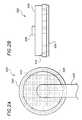
- FIG. 1shows top and side views of a first CMP pad conditioner arrangement, according to an example embodiment of the present invention.
- FIG. 2shows top and side views of a second CMP pad conditioner arrangement, according to another example embodiment of the present invention.
- a CMP pad conditionerincludes a fluid source adapted to supply cleaning elements at a pressure of at least about 20 PSI.
- a dispensing arrangementis coupled to the fluid source and is adapted to dispense the cleaning elements onto a CMP pad. It has been discovered that the above fluid source and dispensing arrangement facilitate cleaning to a depth into a CMP pad that sufficiently addresses current problems associated with CMP pad conditioners including those discussed hereinabove in the Background of the Invention.
- the dispensing arrangementincludes a distribution surface adapted to receive and disperse the cleaning elements, such as liquid or a liquid solution, at high-pressure and high-volume.
- the dispensing arrangementfurther includes a dispenser having a plurality of ports coupled to the distribution surface and adapted receive the cleaning elements, and to pass the cleaning elements onto a CMP pad.
- the cleaning elementsare received at a pressure of at least about 30 PSI for a more difficult and thorough cleaning application.
- the flow rate of the cleaning elementscan vary with the size of the pad conditioner and the number of holes, and typically is above about 1.5 GPM. In this manner, the high-pressure, high-volume cleaning elements improve the cleaning of the pad by drawing particles embedded in the pad up out of the pad and removing them. This cleaning of the pad improves the pad life, reduces the number of defects, and improves the uniformity of the polish rate.
- FIG. 1shows top and side views of a CMP pad conditioner arrangement 100 for use in a CMP process, according to another example embodiment of the present invention.
- a supply 130is configured and arranged to supply cleaning elements to a pad conditioner head 140 .
- Pad conditioner head 140includes holes 110 for receiving cleaning elements at a pressure of at least about 30 PSI and a flow rate of at least about 1.5 GPM, and for dispensing the cleaning elements to the surface to be conditioned.
- Supply 130is further adapted to deliver fluid at the high pressure and flow rates described.
- the holesare between about 1 ⁇ 8 inch and about 1 ⁇ 4 inch in diameter.
- the holesare located at a density of between about 9-36 holes per square inch.
- Brushes 120are coupled to the pad conditioner head 140 .
- the brushesmay, for instance, comprise chemically resistant material, such as plastic or Teflon.
- chemically resistant brushesis particularly advantageous in applications where the cleaning elements include chemicals that are reactive with non-chemically resistant brush material.
- the brushesmay also include material such as metal, diamond, and nickel, and may include chemically inert material.
- chemically inert material for the brushesis particularly useful in connection with the use of cleaning solutions having an acidic or basic nature.
- the CMP pad conditioning arrangement shown in FIG. 1is used to clean and condition a CMP pad.
- Cleaning elementsare delivered to the pad conditioner head 140 by way of supply 130 .
- the cleaning elementsmay include, for example, chemicals ranging in pH from highly basic to highly acidic, or solvents such as de-ionized (DI) water.
- DIde-ionized
- the cleaning elementsare dispersed in the head 140 , and dispensed through holes 110 .
- Brushes 120are coupled to the pad conditioner head 140 , and are caused to contact a rotating CMP pad.
- the CMP padis rotated at a rotational speed sufficiently greater than the speed used for the CMP polishing process such that the cleaning elements and the residual polishing elements are centrifugally removed from the pad.
- a rotational speed of about 50% greater than the polishing speedis useful, for example, for throwing the used slurry off of the CMP pad.
- the cleaning elementsare dispersed onto the CMP pad, and the CMP pad is cleaned and conditioned.
- Cleaning and conditioning the CMP padmay, for instance, also include rotating the pad conditioner head 140 , such as rotating about its center using a motor/axle arrangement (not shown) coupled to the housing for the supply 130 .
- pad conditionersadaptable for use in accordance with the present invention, reference may be made to U.S. Pat. No. 6,302,771, issued on Oct. 16, 2001 (Docket No. VLSI.231PA).
- the pad conditioner arrangement shown in FIG. 1is used in conjunction with a second pad conditioner arrangement adapted to dispense slurry and condition the pad.
- the pad cleaning arrangement of FIG. 1is used to clean the pad of polishing residuals and of the slurry dispensed by the second pad.
- a plurality of CMP pad conditionersare used for supplying slurry, and a plurality of CMP pad conditioners such as shown in FIG. 1 are used to clean the pad, facilitating the polishing of a plurality of wafers at the same time.
- CMP pad shown in FIG. 1can be used for cleaning the plurality of wafers at the same time.
- two wafersare polished using a CMP polishing arrangement having two slurry dispensing pad conditioner arrangements and two cleaning pad conditioner arrangements.
- a first slurry dispensing pad conditionerdispenses slurry and conditions the pad.
- the padis rotated, the slurry is used to polish a first wafer, and is cleaned by a first CMP pad conditioner arrangement, such as shown in FIG. 1, thereby preventing slurry and polishing residuals from reaching the second wafer arrangement.
- a second slurry dispensing pad conditionerdispenses slurry and conditions the pad.
- the padis rotated, the slurry is used to polish the second wafer, and the pad is cleaned by a second CMP pad conditioner arrangement, such as shown in FIG. 1, thereby preventing slurry and polishing residuals from reaching the first wafer as the pad rotates.
- a second CMP pad conditioner arrangementsuch as shown in FIG. 1, thereby preventing slurry and polishing residuals from reaching the first wafer as the pad rotates.
- a semiconductor waferis manufactured using the CMP pad conditioner and pad described in the above paragraph. After the pad is cleaned and conditioned, a slurry is introduced to the pad and the pad is caused to rotate. The semiconductor wafer is held face-down, brought into contact with the slurry and the pad, and polished.
- FIG. 2shows top and side views of a CMP pad conditioner arrangement 200 for use in a CMP process, according to another example embodiment of the present invention.
- the CMP pad conditioner arrangement 200is similar to the CMP pad arrangement 100 shown in FIG. 1, except having a grid arrangement 220 in place of the brushes 120 .
- Grid arrangement 220is coupled to the pad conditioner head 240 and may include, for instance, material such as metal, plastic, Teflon, diamond, or CVD diamond coated with Nickel.
- the CMP pad conditioning arrangement 200is used to clean and condition a CMP pad.
- supply 230is coupled to pad conditioner head 240 .
- Cleaning elementsare delivered to the pad conditioner head 240 by way of supply 230 .
- the cleaning elementsare dispersed in the head 240 , and dispensed through holes 210 at a pressure of at least about 30 PSI and a flow rate of at least about 1.5 GPM.
- Grid arrangement 220is coupled to pad conditioner head 240 , and is caused to contact a CMP pad.
- the cleaning elementsare dispersed onto the CMP pad, and the CMP pad is cleaned and conditioned.
- Cleaning and conditioning the CMP padmay, for instance, also include rotating the pad conditioner head 240 , in a manner such as rotating about its center using a motor/axle arrangement (not shown) coupled to the housing for the supply 230 .
Landscapes
- Engineering & Computer Science (AREA)
- Mechanical Engineering (AREA)
- Mechanical Treatment Of Semiconductor (AREA)
- Grinding-Machine Dressing And Accessory Apparatuses (AREA)
Abstract
Description
Claims (28)
Priority Applications (1)
| Application Number | Priority Date | Filing Date | Title |
|---|---|---|---|
| US09/490,466US6331136B1 (en) | 2000-01-25 | 2000-01-25 | CMP pad conditioner arrangement and method therefor |
Applications Claiming Priority (1)
| Application Number | Priority Date | Filing Date | Title |
|---|---|---|---|
| US09/490,466US6331136B1 (en) | 2000-01-25 | 2000-01-25 | CMP pad conditioner arrangement and method therefor |
Publications (1)
| Publication Number | Publication Date |
|---|---|
| US6331136B1true US6331136B1 (en) | 2001-12-18 |
Family
ID=23948173
Family Applications (1)
| Application Number | Title | Priority Date | Filing Date |
|---|---|---|---|
| US09/490,466Expired - Fee RelatedUS6331136B1 (en) | 2000-01-25 | 2000-01-25 | CMP pad conditioner arrangement and method therefor |
Country Status (1)
| Country | Link |
|---|---|
| US (1) | US6331136B1 (en) |
Cited By (25)
| Publication number | Priority date | Publication date | Assignee | Title |
|---|---|---|---|---|
| US6640795B1 (en)* | 1999-09-29 | 2003-11-04 | Kabushiki Kaisha Toshiba | Dresser, polishing apparatus and method for producing an article |
| US20040038632A1 (en)* | 2002-08-23 | 2004-02-26 | Chi-Feng Cheng | Conditioner of chemical-mechanical polishing station |
| US6773337B1 (en)* | 2000-11-07 | 2004-08-10 | Planar Labs Corporation | Method and apparatus to recondition an ion exchange polish pad |
| US20040157538A1 (en)* | 2003-02-11 | 2004-08-12 | Suresh Ramarajan | Apparatuses and methods for conditioning polishing pads used in polishing micro-device workpieces |
| US20040198184A1 (en)* | 2001-08-24 | 2004-10-07 | Joslyn Michael J | Planarizing machines and methods for dispensing planarizing solutions in the processing of microelectronic workpieces |
| US20040241989A1 (en)* | 2003-05-29 | 2004-12-02 | Benner Stephen J. | Method of using multiple, different slurries in a CMP polishing process via a pad conditioning system |
| US20050266688A1 (en)* | 2004-05-25 | 2005-12-01 | Fujitsu Limited | Semiconductor device fabrication method |
| US6994611B2 (en)* | 1999-05-28 | 2006-02-07 | Lam Research Corporation | Method and system for cleaning a chemical mechanical polishing pad |
| US20060046623A1 (en)* | 2004-08-24 | 2006-03-02 | Applied Materials, Inc. | Method and apparatus for reduced wear polishing pad conditioning |
| US7033253B2 (en) | 2004-08-12 | 2006-04-25 | Micron Technology, Inc. | Polishing pad conditioners having abrasives and brush elements, and associated systems and methods |
| US20060156830A1 (en)* | 2002-12-06 | 2006-07-20 | Endress + Hauser Flowtec Ag | Process meter |
| US20070087672A1 (en)* | 2005-10-19 | 2007-04-19 | Tbw Industries, Inc. | Apertured conditioning brush for chemical mechanical planarization systems |
| US20080092734A1 (en)* | 2006-10-07 | 2008-04-24 | Tbw Industries Inc. | Vacuum line clean-out separator system |
| US20090127231A1 (en)* | 2007-11-08 | 2009-05-21 | Chien-Min Sung | Methods of Forming Superhard Cutters and Superhard Cutters Formed Thereby |
| US7544113B1 (en)* | 2003-05-29 | 2009-06-09 | Tbw Industries, Inc. | Apparatus for controlling the forces applied to a vacuum-assisted pad conditioning system |
| US20090239456A1 (en)* | 2008-03-24 | 2009-09-24 | Phuong Van Nguyen | Chemical Mechanical Polishing Pad and Dresser |
| US20100132687A1 (en)* | 2007-01-16 | 2010-06-03 | John Budiac | Adjustable material cutting guide system |
| US20110003538A1 (en)* | 2006-02-06 | 2011-01-06 | Chien-Min Sung | Pad Conditioner Dresser |
| US8142261B1 (en)* | 2006-11-27 | 2012-03-27 | Chien-Min Sung | Methods for enhancing chemical mechanical polishing pad processes |
| DE102012206708A1 (en) | 2012-04-24 | 2013-10-24 | Siltronic Ag | Method for polishing semiconductor wafer, involves providing functional layer of polishing cloth with pores and small blind holes which are arranged in radially inward region and radially outward region |
| USD793971S1 (en) | 2015-03-27 | 2017-08-08 | Veeco Instruments Inc. | Wafer carrier with a 14-pocket configuration |
| USD793972S1 (en)* | 2015-03-27 | 2017-08-08 | Veeco Instruments Inc. | Wafer carrier with a 31-pocket configuration |
| USD806046S1 (en) | 2015-04-16 | 2017-12-26 | Veeco Instruments Inc. | Wafer carrier with a multi-pocket configuration |
| CN109108800A (en)* | 2018-08-13 | 2019-01-01 | 芜湖九鼎电子科技有限公司 | A kind of full-automatic instrument mirro finished machine |
| US11135612B2 (en)* | 2019-03-19 | 2021-10-05 | The Boeing Company | Rotating applicators having fluid dispensers |
Citations (9)
| Publication number | Priority date | Publication date | Assignee | Title |
|---|---|---|---|---|
| US5456627A (en)* | 1993-12-20 | 1995-10-10 | Westech Systems, Inc. | Conditioner for a polishing pad and method therefor |
| US5531635A (en)* | 1994-03-23 | 1996-07-02 | Mitsubishi Materials Corporation | Truing apparatus for wafer polishing pad |
| US5547417A (en)* | 1994-03-21 | 1996-08-20 | Intel Corporation | Method and apparatus for conditioning a semiconductor polishing pad |
| US5611943A (en)* | 1995-09-29 | 1997-03-18 | Intel Corporation | Method and apparatus for conditioning of chemical-mechanical polishing pads |
| US5616069A (en)* | 1995-12-19 | 1997-04-01 | Micron Technology, Inc. | Directional spray pad scrubber |
| US5868608A (en)* | 1996-08-13 | 1999-02-09 | Lsi Logic Corporation | Subsonic to supersonic and ultrasonic conditioning of a polishing pad in a chemical mechanical polishing apparatus |
| US5885147A (en)* | 1997-05-12 | 1999-03-23 | Integrated Process Equipment Corp. | Apparatus for conditioning polishing pads |
| US5916010A (en)* | 1997-10-30 | 1999-06-29 | International Business Machines Corporation | CMP pad maintenance apparatus and method |
| US6179693B1 (en)* | 1998-10-06 | 2001-01-30 | International Business Machines Corporation | In-situ/self-propelled polishing pad conditioner and cleaner |
- 2000
- 2000-01-25USUS09/490,466patent/US6331136B1/ennot_activeExpired - Fee Related
Patent Citations (9)
| Publication number | Priority date | Publication date | Assignee | Title |
|---|---|---|---|---|
| US5456627A (en)* | 1993-12-20 | 1995-10-10 | Westech Systems, Inc. | Conditioner for a polishing pad and method therefor |
| US5547417A (en)* | 1994-03-21 | 1996-08-20 | Intel Corporation | Method and apparatus for conditioning a semiconductor polishing pad |
| US5531635A (en)* | 1994-03-23 | 1996-07-02 | Mitsubishi Materials Corporation | Truing apparatus for wafer polishing pad |
| US5611943A (en)* | 1995-09-29 | 1997-03-18 | Intel Corporation | Method and apparatus for conditioning of chemical-mechanical polishing pads |
| US5616069A (en)* | 1995-12-19 | 1997-04-01 | Micron Technology, Inc. | Directional spray pad scrubber |
| US5868608A (en)* | 1996-08-13 | 1999-02-09 | Lsi Logic Corporation | Subsonic to supersonic and ultrasonic conditioning of a polishing pad in a chemical mechanical polishing apparatus |
| US5885147A (en)* | 1997-05-12 | 1999-03-23 | Integrated Process Equipment Corp. | Apparatus for conditioning polishing pads |
| US5916010A (en)* | 1997-10-30 | 1999-06-29 | International Business Machines Corporation | CMP pad maintenance apparatus and method |
| US6179693B1 (en)* | 1998-10-06 | 2001-01-30 | International Business Machines Corporation | In-situ/self-propelled polishing pad conditioner and cleaner |
Non-Patent Citations (2)
| Title |
|---|
| U.S. Pat. application No. 09/283,049, "CMP Pad Conditioner Arrangement and Method Therefor," Filing Date Apr. 1, 1999. |
| U.S. Pat. application No. 09/283,716, "Dual CMP Pad Conditioner," Filing Date Apr. 1, 1999. |
Cited By (41)
| Publication number | Priority date | Publication date | Assignee | Title |
|---|---|---|---|---|
| US6994611B2 (en)* | 1999-05-28 | 2006-02-07 | Lam Research Corporation | Method and system for cleaning a chemical mechanical polishing pad |
| US6640795B1 (en)* | 1999-09-29 | 2003-11-04 | Kabushiki Kaisha Toshiba | Dresser, polishing apparatus and method for producing an article |
| US6773337B1 (en)* | 2000-11-07 | 2004-08-10 | Planar Labs Corporation | Method and apparatus to recondition an ion exchange polish pad |
| US7210989B2 (en) | 2001-08-24 | 2007-05-01 | Micron Technology, Inc. | Planarizing machines and methods for dispensing planarizing solutions in the processing of microelectronic workpieces |
| US20040198184A1 (en)* | 2001-08-24 | 2004-10-07 | Joslyn Michael J | Planarizing machines and methods for dispensing planarizing solutions in the processing of microelectronic workpieces |
| US20040038632A1 (en)* | 2002-08-23 | 2004-02-26 | Chi-Feng Cheng | Conditioner of chemical-mechanical polishing station |
| US20060156830A1 (en)* | 2002-12-06 | 2006-07-20 | Endress + Hauser Flowtec Ag | Process meter |
| US7708622B2 (en) | 2003-02-11 | 2010-05-04 | Micron Technology, Inc. | Apparatuses and methods for conditioning polishing pads used in polishing micro-device workpieces |
| US7997958B2 (en) | 2003-02-11 | 2011-08-16 | Micron Technology, Inc. | Apparatuses and methods for conditioning polishing pads used in polishing micro-device workpieces |
| US6884152B2 (en)* | 2003-02-11 | 2005-04-26 | Micron Technology, Inc. | Apparatuses and methods for conditioning polishing pads used in polishing micro-device workpieces |
| US20040157538A1 (en)* | 2003-02-11 | 2004-08-12 | Suresh Ramarajan | Apparatuses and methods for conditioning polishing pads used in polishing micro-device workpieces |
| US7052371B2 (en)* | 2003-05-29 | 2006-05-30 | Tbw Industries Inc. | Vacuum-assisted pad conditioning system and method utilizing an apertured conditioning disk |
| US8025555B1 (en)* | 2003-05-29 | 2011-09-27 | Tbw Industries Inc. | System for measuring and controlling the level of vacuum applied to a conditioning holder within a CMP system |
| US7575503B2 (en)* | 2003-05-29 | 2009-08-18 | Tbw Industries, Inc. | Vacuum-assisted pad conditioning system |
| WO2004112091A3 (en)* | 2003-05-29 | 2005-03-24 | Tbw Ind Inc | Vacuum-assisted pad conditioning system and method utilizing an apertured conditioning disk |
| US7258600B1 (en)* | 2003-05-29 | 2007-08-21 | Tbw Industries, Inc. | Vacuum-assisted pad conditioning system |
| US20070281592A1 (en)* | 2003-05-29 | 2007-12-06 | Benner Stephen J | Vacuum-assisted pad conditioning system and method utilizing an apertured conditioning disk |
| US7901267B1 (en)* | 2003-05-29 | 2011-03-08 | Tbw Industries, Inc. | Method for controlling the forces applied to a vacuum-assisted pad conditioning system |
| US20040241989A1 (en)* | 2003-05-29 | 2004-12-02 | Benner Stephen J. | Method of using multiple, different slurries in a CMP polishing process via a pad conditioning system |
| US7544113B1 (en)* | 2003-05-29 | 2009-06-09 | Tbw Industries, Inc. | Apparatus for controlling the forces applied to a vacuum-assisted pad conditioning system |
| US20050266688A1 (en)* | 2004-05-25 | 2005-12-01 | Fujitsu Limited | Semiconductor device fabrication method |
| US7033253B2 (en) | 2004-08-12 | 2006-04-25 | Micron Technology, Inc. | Polishing pad conditioners having abrasives and brush elements, and associated systems and methods |
| US20060046623A1 (en)* | 2004-08-24 | 2006-03-02 | Applied Materials, Inc. | Method and apparatus for reduced wear polishing pad conditioning |
| US7210988B2 (en)* | 2004-08-24 | 2007-05-01 | Applied Materials, Inc. | Method and apparatus for reduced wear polishing pad conditioning |
| US20070087672A1 (en)* | 2005-10-19 | 2007-04-19 | Tbw Industries, Inc. | Apertured conditioning brush for chemical mechanical planarization systems |
| US8298043B2 (en) | 2006-02-06 | 2012-10-30 | Chien-Min Sung | Pad conditioner dresser |
| US20110003538A1 (en)* | 2006-02-06 | 2011-01-06 | Chien-Min Sung | Pad Conditioner Dresser |
| US20080092734A1 (en)* | 2006-10-07 | 2008-04-24 | Tbw Industries Inc. | Vacuum line clean-out separator system |
| US7909910B2 (en) | 2006-10-07 | 2011-03-22 | Tbw Industries Inc. | Vacuum line clean-out separator system |
| US8142261B1 (en)* | 2006-11-27 | 2012-03-27 | Chien-Min Sung | Methods for enhancing chemical mechanical polishing pad processes |
| US20100132687A1 (en)* | 2007-01-16 | 2010-06-03 | John Budiac | Adjustable material cutting guide system |
| US20090127231A1 (en)* | 2007-11-08 | 2009-05-21 | Chien-Min Sung | Methods of Forming Superhard Cutters and Superhard Cutters Formed Thereby |
| US20090239456A1 (en)* | 2008-03-24 | 2009-09-24 | Phuong Van Nguyen | Chemical Mechanical Polishing Pad and Dresser |
| US8182315B2 (en)* | 2008-03-24 | 2012-05-22 | Phuong Van Nguyen | Chemical mechanical polishing pad and dresser |
| DE102012206708A1 (en) | 2012-04-24 | 2013-10-24 | Siltronic Ag | Method for polishing semiconductor wafer, involves providing functional layer of polishing cloth with pores and small blind holes which are arranged in radially inward region and radially outward region |
| USD793971S1 (en) | 2015-03-27 | 2017-08-08 | Veeco Instruments Inc. | Wafer carrier with a 14-pocket configuration |
| USD793972S1 (en)* | 2015-03-27 | 2017-08-08 | Veeco Instruments Inc. | Wafer carrier with a 31-pocket configuration |
| USD852762S1 (en) | 2015-03-27 | 2019-07-02 | Veeco Instruments Inc. | Wafer carrier with a 14-pocket configuration |
| USD806046S1 (en) | 2015-04-16 | 2017-12-26 | Veeco Instruments Inc. | Wafer carrier with a multi-pocket configuration |
| CN109108800A (en)* | 2018-08-13 | 2019-01-01 | 芜湖九鼎电子科技有限公司 | A kind of full-automatic instrument mirro finished machine |
| US11135612B2 (en)* | 2019-03-19 | 2021-10-05 | The Boeing Company | Rotating applicators having fluid dispensers |
Similar Documents
| Publication | Publication Date | Title |
|---|---|---|
| US6331136B1 (en) | CMP pad conditioner arrangement and method therefor | |
| US6302771B1 (en) | CMP pad conditioner arrangement and method therefor | |
| US5611943A (en) | Method and apparatus for conditioning of chemical-mechanical polishing pads | |
| US6368194B1 (en) | Apparatus for controlling PH during planarization and cleaning of microelectronic substrates | |
| US8485863B2 (en) | Polishing liquids for activating and/or conditioning fixed abrasive polishing pads, and associated systems and methods | |
| KR100509659B1 (en) | Semiconductor device substrate polishing process | |
| US7997958B2 (en) | Apparatuses and methods for conditioning polishing pads used in polishing micro-device workpieces | |
| US6022266A (en) | In-situ pad conditioning process for CMP | |
| JP3676030B2 (en) | Polishing pad dressing method and semiconductor device manufacturing method | |
| US6350183B2 (en) | High pressure cleaning | |
| US20040241989A1 (en) | Method of using multiple, different slurries in a CMP polishing process via a pad conditioning system | |
| JPH1170464A (en) | Combination of slurry dispenser and rinse arm, and operation method | |
| US9475170B2 (en) | Device for cleaning fixed abrasives polishing pad | |
| KR19980087365A (en) | Semiconductor polishing method and apparatus | |
| US6695684B2 (en) | Chemical mechanical polishing apparatus having a cleaner for cleaning a conditioning disc and method of conditioning a polishing pad of the apparatus | |
| US7037178B2 (en) | Methods for conditioning surfaces of polishing pads after chemical-mechanical polishing | |
| JPH1094964A (en) | Cmp device of semiconductor wafer | |
| US6390902B1 (en) | Multi-conditioner arrangement of a CMP system | |
| EP1069972A1 (en) | Apparatus and methods for slurry removal in chemical mechanical polishing | |
| JPH10202507A (en) | Chemical mechanical polishing (CMP) apparatus and chemical mechanical polishing method using the same | |
| EP1190455A2 (en) | Dual cmp pad conditioner | |
| JP3708740B2 (en) | Polishing apparatus and polishing method | |
| JPH09285957A (en) | Abrasive material, polishing method and apparatus using the same | |
| US20080220698A1 (en) | Systems and methods for efficient slurry application for chemical mechanical polishing | |
| JPH10118916A (en) | Chemical mechanical polishing method and device |
Legal Events
| Date | Code | Title | Description |
|---|---|---|---|
| AS | Assignment | Owner name:VLSI TECHNOLOGY, INC., CALIFORNIA Free format text:ASSIGNMENT OF ASSIGNORS INTEREST;ASSIGNORS:BASS, VICTOR J.;VINES, LANDON;REEL/FRAME:010566/0632;SIGNING DATES FROM 20000114 TO 20000117 | |
| FPAY | Fee payment | Year of fee payment:4 | |
| AS | Assignment | Owner name:NXP B.V., NETHERLANDS Free format text:ASSIGNMENT OF ASSIGNORS INTEREST;ASSIGNOR:PHILIPS ELECTRONICS NORTH AMERICA CORP.;REEL/FRAME:018654/0521 Effective date:20061213 | |
| FPAY | Fee payment | Year of fee payment:8 | |
| AS | Assignment | Owner name:PHILIPS SEMICONDUCTORS INC., NEW YORK Free format text:CHANGE OF NAME;ASSIGNOR:PHILIPS SEMICONDUCTORS VLSI INC.;REEL/FRAME:027165/0627 Effective date:19991220 Owner name:PHILIPS SEMICONDUCTORS VLSI INC., NEW YORK Free format text:CHANGE OF NAME;ASSIGNOR:VLSI TECHNOLOGY, INC.;REEL/FRAME:027161/0796 Effective date:19990702 | |
| AS | Assignment | Owner name:PHILIPS ELECTRONICS NORTH AMERICA CORPORATION, MAS Free format text:NUNC PRO TUNC ASSIGNMENT;ASSIGNOR:PHILIPS SEMICONDUCTORS INC.;REEL/FRAME:027264/0580 Effective date:20111107 | |
| REMI | Maintenance fee reminder mailed | ||
| LAPS | Lapse for failure to pay maintenance fees | ||
| STCH | Information on status: patent discontinuation | Free format text:PATENT EXPIRED DUE TO NONPAYMENT OF MAINTENANCE FEES UNDER 37 CFR 1.362 | |
| FP | Lapsed due to failure to pay maintenance fee | Effective date:20131218 |