US6330654B1 - Memory cache with sequential page indicators - Google Patents
Memory cache with sequential page indicatorsDownload PDFInfo
- Publication number
- US6330654B1 US6330654B1US09/383,468US38346899AUS6330654B1US 6330654 B1US6330654 B1US 6330654B1US 38346899 AUS38346899 AUS 38346899AUS 6330654 B1US6330654 B1US 6330654B1
- Authority
- US
- United States
- Prior art keywords
- memory
- page
- sequential
- field
- identified
- Prior art date
- Legal status (The legal status is an assumption and is not a legal conclusion. Google has not performed a legal analysis and makes no representation as to the accuracy of the status listed.)
- Expired - Lifetime
Links
Images


Classifications
- G—PHYSICS
- G06—COMPUTING OR CALCULATING; COUNTING
- G06F—ELECTRIC DIGITAL DATA PROCESSING
- G06F12/00—Accessing, addressing or allocating within memory systems or architectures
- G06F12/02—Addressing or allocation; Relocation
- G06F12/08—Addressing or allocation; Relocation in hierarchically structured memory systems, e.g. virtual memory systems
- G06F12/10—Address translation
- G06F12/1027—Address translation using associative or pseudo-associative address translation means, e.g. translation look-aside buffer [TLB]
- G—PHYSICS
- G09—EDUCATION; CRYPTOGRAPHY; DISPLAY; ADVERTISING; SEALS
- G09G—ARRANGEMENTS OR CIRCUITS FOR CONTROL OF INDICATING DEVICES USING STATIC MEANS TO PRESENT VARIABLE INFORMATION
- G09G5/00—Control arrangements or circuits for visual indicators common to cathode-ray tube indicators and other visual indicators
- G09G5/36—Control arrangements or circuits for visual indicators common to cathode-ray tube indicators and other visual indicators characterised by the display of a graphic pattern, e.g. using an all-points-addressable [APA] memory
- G09G5/39—Control of the bit-mapped memory
- G—PHYSICS
- G09—EDUCATION; CRYPTOGRAPHY; DISPLAY; ADVERTISING; SEALS
- G09G—ARRANGEMENTS OR CIRCUITS FOR CONTROL OF INDICATING DEVICES USING STATIC MEANS TO PRESENT VARIABLE INFORMATION
- G09G2360/00—Aspects of the architecture of display systems
- G09G2360/12—Frame memory handling
- G—PHYSICS
- G09—EDUCATION; CRYPTOGRAPHY; DISPLAY; ADVERTISING; SEALS
- G09G—ARRANGEMENTS OR CIRCUITS FOR CONTROL OF INDICATING DEVICES USING STATIC MEANS TO PRESENT VARIABLE INFORMATION
- G09G2360/00—Aspects of the architecture of display systems
- G09G2360/12—Frame memory handling
- G09G2360/125—Frame memory handling using unified memory architecture [UMA]
Definitions
- the inventionrelates generally to computer system memory architectures and more particularly, but not by way of limitation, to a translation-lookaside buffer incorporating sequential physical memory page indications.
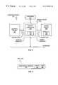
- conventional computer system 100providing accelerated graphics port (AGP) capability includes graphics accelerator 102 coupled to graphics device 104 , local frame buffer memory 106 , and bridge circuit 108 .
- Bridge circuit 108provides electrical and functional coupling between graphics accelerator 102 , system memory 110 , processor 112 , and system bus 114 .
- computer system 100may be a special purpose graphics workstation, a desktop personal computer or a portable personal computer
- graphics device 104may be a display monitor
- processor 112may be a PENTIUM® processor
- system memory 110may be synchronous dynamic random access memory (SDRAM)
- system bus 114may operate in conformance with the Peripheral Component Interconnect (PCI) specification.
- PCIPeripheral Component Interconnect
- graphics accelerator 102may use both local frame buffer 106 and system memory 110 as primary graphics memory. (See the Accelerated Graphics Port Interface Specification, revision 2.0, 1998, available from Intel Corporation.) As a consequence, AGP bus 116 operations tend to be short, random accesses. Because graphics accelerator 102 may generate direct references into system memory 110 , a contiguous view of system memory is needed. However, since system memory 110 is dynamically allocated (typically in 4 kilobyte pages), it is generally not possible to provide graphics accelerator 102 with a single continuous memory region within system memory 110 . Thus, it is necessary to provide an address remapping mechanism which insures graphics accelerator 102 will have a contiguous view of graphics data structures dynamically allocated and stored in system memory 110 .
- GARTGraphics Address Remapping Table
- bridge circuit 108commonly caches up to a specified maximum number (e.g., 32) of GART page table entries in translation-lookaside buffer 120 (TLB, see FIG. 1 ).
- TLB 120translation-lookaside buffer 120
- a cache missoccurs.
- that page table entry in GART 118 providing the necessary address remapping informationis identified, retrieved by bridge circuit 108 , used to obtain the requested data, and replaces a selected entry in TLB 120 .
- the specific page table entry in TLB 120 to replacemay be determined by any desired replacement algorithm. For example, least recently used or working set cache replacement algorithms may be used.
- Each TLB cache missmay cause graphics accelerator 102 to temporarily slow or stop processing. Thus, it would be beneficial to provide a mechanism to reduce the number of TLB cache miss operations.
- the inventionprovides a memory (having a plurality of page table entry (PTE) data structures) for storing address translation data.
- PTE data structureincludes a base address field to identify an allocated page of memory, a prior page field to identify zero or more allocated pages of memory that are sequential to and before that page of memory identified by the base address field, and a subsequent page field to identify zero or more allocated pages of memory that are sequential to and after that page identified by the base address field.
- the inventionprovides a computer system bridge circuit incorporating an address translation memory as described above.
- the inventionprovides a computer system incorporating an address translation memory as described above.
- FIG. 1shows a prior art graphics capable computer system.
- FIG. 2illustrates how a Graphics Address Remapping Table (GART) maps a contiguous range of physical addresses to a series of non-contiguous pages in system memory.
- GARTGraphics Address Remapping Table
- FIG. 3shows a computer system incorporating a GART and translation-lookaside buffer cache in accordance with one embodiment of the invention.
- FIG. 4shows a page table entry in accordance with one embodiment of the invention.
- FIG. 5shows a GART having N page table entries representing N sequentially allocated pages of memory in accordance with one embodiment of the invention.
- FIG. 6shows a logical to physical address translation technique using page table entries in accordance with the invention.
- a cachewhose entries indicate the amount of allocated physical memory that is sequential to (before and after) that memory identified by the cache entry is described.
- AGPAccelerated Graphics Port
- TLBtranslation-lookaside buffer
- Graphics Address Remapping Table (GART) 300 and TLB 302 in accordance with one embodiment of the inventionare elements of graphics capable computer system 304 .
- Each page (typically 4 kilobytes in size) of system memory 306 allocated to graphics engine 308has a page table entry in GART 300 .
- Memory controller 310may use TLB 302 to cache a selected subset of GART page table entries.
- TLB 302may include a maximum of 32 entries.
- TLB entriesare stored in special purpose hardware registers in memory controller 310 .
- TLB entriesmay be stored in random access memory internal to memory controller 310 (or bridge circuit 316 ).
- computer system 304may further include one or more processor units 312 and system bus 314 . Further, memory controller 310 may be incorporated within bridge circuit 316 .
- Graphics engine 308typically requests, and is allocated, multiple pages of memory at a time. Because of this, it is often the case that a number of sequential physical memory pages are allocated to graphics engine 308 . This sequential characteristic of allocated system memory may be recorded in GART 300 and TLB 302 and used by memory controller 310 to effectively extend the number of page table entries covered by TLB 302 . This, in turn, may reduce the number of TLB cache miss operations and thereby improve computer system performance.
- page table entry (PTE) 400in accordance with one embodiment of the invention includes base physical address field 402 , prior sequential page field 404 , and subsequent sequential page field 406 .
- Base physical address field 402represents the physical address of an allocated page in system memory 306 .
- Prior sequential page field 404indicates the number of allocated pages that are sequential to and before (i.e., having a lower memory address) that page identified in base physical address field 402 .
- Subsequent page indication field 406indicates the number of allocated pages that are sequential to and after (i.e., having a higher memory address) that page identified in base physical address field 402 .
- prior and sequential page indication fields 404 and 406may encode a value representing the number of prior and subsequent sequential pages. In this embodiment, 8-bit fields provide sufficient range to span 510 pages of memory—nearly 2 megabytes (255 prior pages and 255 subsequent pages). In another embodiment, prior and sequential page indication fields 404 and 406 may encode the page address of the first and last pages respectively in the sequence of allocated pages. In this embodiment, prior and subsequent sequential page fields are large enough to encode a page address (e.g., 20 bits).
- N sequentially allocated pages of memorymay be represented in GART 300 by N page table entries. If prior and subsequent sequential page fields 404 and 406 encode a page count, the first of the N page table entries ( 500 ) will have a prior sequential page field ( 502 ) value of 0 to indicate there are no allocated pages of memory prior and sequential to the page identified by base physical address field 504 , and a subsequent sequential page field ( 506 ) value of N ⁇ 1 to indicate there are N ⁇ 1 allocated pages of memory following and sequential to the page identified by base physical address field 504 .
- the last of the N page table entries ( 508 )has a prior sequential page field ( 510 ) value of N ⁇ 1 to indicate there are N ⁇ 1 allocated pages of memory prior and sequential to the page identified by base physical address field 512 , and a subsequent sequential page field ( 514 ) value of 0 indicating there are no allocated pages of memory following and sequential to the page identified by base physical address field 512 .
- a PTE corresponding to an allocated page of memory that is not sequential to another allocated page of memoryhas prior ( 404 ) and subsequent ( 406 ) field entry values of 0.
- memory controller 310may calculate the starting and ending physical address of any sequential block of allocated memory, the starting and ending logical addresses corresponding to those physical addresses (e.g., those addresses received by memory controller 310 from graphics engine 308 ), and the relative offset between a logical and physical address. Thus, using any one PTE from a sequential series of allocated memory pages, memory controller 310 may use the entry's prior ( 404 ) and subsequent ( 406 ) field values to perform address translation for any logical address in the range spanned by the sequential memory block.
- a memory access operationis initiated when memory controller 310 receives a logical address from graphics engine 308 (block 600 ).
- Memory controller 310determines if the received logical address corresponds to an entry in TLB 302 (diamond 602 ).
- the requested pagemay be said to be covered by TLB 302 if any entry therein: (1) has a base physical address corresponding to the requested page, or (2) encompasses the requested page when its base physical address is expanded to incorporate those pages indicated by its prior or subsequent sequential page fields. If the requested page is covered by TLB 302 (the “yes” prong of diamond 602 ), the logical address may be immediately translated (block 604 ) and the resulting physical address used to access system memory 310 (block 606 ).
- memory controllerretrieves the appropriate page table entry from GART 300 (block 608 ). If TLB 302 has space available for the new PTE (the “yes” prong of diamond 610 ), the new PTE is stored (block 612 ), the received logical address is translated (block 604 ), and the resulting physical address is used to access system memory (block 606 ). If TLB 302 does not have space available for the new PTE (the “no” prong of diamond 610 ), an existing entry in TLB 302 is selectively replaced by that entry retrieved during the act of block 608 (block 614 ). While any cache replacement algorithm may be used, an industry standard technique is to replace that TLB cache entry that was least recently used. Once TLB 302 has been updated, address translation and memory access may proceed as indicated in blocks 604 and 606 .
- page table entries in accordance with the inventionare that multiple sequentially allocated pages may be represented by a single TLB entry in memory controller 310 . This may allow a TLB of a given size to provide better coverage (i.e., a higher cache hit rate) than a prior art TLB not using prior and subsequent field entries. This, in turn, may improve system performance when address translation is required.
- Another benefit of a page table entry in accordance with the inventionis that their use may reduce the number of TLB entries cached in memory controller 310 , thereby conserving memory resources within bridge circuit 316 .
- a circuit to maintain TLB 302may be integral to memory controller 310 as described herein, or it may be distinct from memory controller. That is, TLB control may be performed by a circuit that interfaces to memory controller 310 . Further, memory controller 310 and/or a TLB maintenance circuit may be incorporated within bridge circuit 316 (typically implemented as an application specific integrated circuits, or ASIC), or it may be a stand-alone circuit, or it may be incorporated within a memory module providing system memory 306 . It is intended, therefore, that the following claims cover all such modifications and variations that may fall within the true sprit and scope of the invention.
Landscapes
- Engineering & Computer Science (AREA)
- Theoretical Computer Science (AREA)
- Physics & Mathematics (AREA)
- General Physics & Mathematics (AREA)
- General Engineering & Computer Science (AREA)
- Computer Hardware Design (AREA)
- Memory System Of A Hierarchy Structure (AREA)
Abstract
Description
Claims (18)
Priority Applications (2)
| Application Number | Priority Date | Filing Date | Title |
|---|---|---|---|
| US09/383,468US6330654B1 (en) | 1999-08-26 | 1999-08-26 | Memory cache with sequential page indicators |
| US09/933,318US6526497B1 (en) | 1999-08-26 | 2001-08-20 | Memory cache with sequential page indicators |
Applications Claiming Priority (1)
| Application Number | Priority Date | Filing Date | Title |
|---|---|---|---|
| US09/383,468US6330654B1 (en) | 1999-08-26 | 1999-08-26 | Memory cache with sequential page indicators |
Related Child Applications (1)
| Application Number | Title | Priority Date | Filing Date |
|---|---|---|---|
| US09/933,318ContinuationUS6526497B1 (en) | 1999-08-26 | 2001-08-20 | Memory cache with sequential page indicators |
Publications (1)
| Publication Number | Publication Date |
|---|---|
| US6330654B1true US6330654B1 (en) | 2001-12-11 |
Family
ID=23513302
Family Applications (2)
| Application Number | Title | Priority Date | Filing Date |
|---|---|---|---|
| US09/383,468Expired - LifetimeUS6330654B1 (en) | 1999-08-26 | 1999-08-26 | Memory cache with sequential page indicators |
| US09/933,318Expired - LifetimeUS6526497B1 (en) | 1999-08-26 | 2001-08-20 | Memory cache with sequential page indicators |
Family Applications After (1)
| Application Number | Title | Priority Date | Filing Date |
|---|---|---|---|
| US09/933,318Expired - LifetimeUS6526497B1 (en) | 1999-08-26 | 2001-08-20 | Memory cache with sequential page indicators |
Country Status (1)
| Country | Link |
|---|---|
| US (2) | US6330654B1 (en) |
Cited By (15)
| Publication number | Priority date | Publication date | Assignee | Title |
|---|---|---|---|---|
| US20020118204A1 (en)* | 1999-07-02 | 2002-08-29 | Milivoje Aleksic | System of accessing data in a graphics system and method thereof |
| US6546449B1 (en)* | 1999-07-02 | 2003-04-08 | Ati International Srl | Video controller for accessing data in a system and method thereof |
| US6674441B1 (en)* | 2000-07-26 | 2004-01-06 | Ati International, Srl | Method and apparatus for improving performance of an accelerated graphics port (AGP) device |
| US6697076B1 (en)* | 2001-12-31 | 2004-02-24 | Apple Computer, Inc. | Method and apparatus for address re-mapping |
| US6820158B1 (en)* | 1999-08-30 | 2004-11-16 | Intel Corporation | Method and apparatus for a configuration ring |
| US20060044934A1 (en)* | 2004-09-02 | 2006-03-02 | Micron Technology, Inc. | Cluster based non-volatile memory translation layer |
| US7034849B1 (en) | 2001-12-31 | 2006-04-25 | Apple Computer, Inc. | Method and apparatus for image blending |
| US20060271725A1 (en)* | 2005-05-24 | 2006-11-30 | Micron Technology, Inc. | Version based non-volatile memory translation layer |
| US7519781B1 (en)* | 2005-12-19 | 2009-04-14 | Nvidia Corporation | Physically-based page characterization data |
| US7681013B1 (en) | 2001-12-31 | 2010-03-16 | Apple Inc. | Method for variable length decoding using multiple configurable look-up tables |
| US7809904B1 (en) | 2005-12-19 | 2010-10-05 | Nvidia Corporation | Page preloading using page characterization data |
| US8639892B1 (en) | 2005-12-19 | 2014-01-28 | Nvidia Corporation | Selectively inhibit page usage bit updates |
| US10664409B2 (en)* | 2018-01-16 | 2020-05-26 | SK Hynix Inc. | Data storage apparatus utilizing sequential map entry for responding to read request and operating method thereof |
| US11042317B2 (en)* | 2018-09-10 | 2021-06-22 | SK Hynix Inc. | Memory system for reducing fragmentation based on sequential index and operating method thereof |
| US11126552B2 (en)* | 2019-04-23 | 2021-09-21 | SK Hynix Inc. | Memory system, memory controller and method for operating memory controller |
Families Citing this family (4)
| Publication number | Priority date | Publication date | Assignee | Title |
|---|---|---|---|---|
| US6633967B1 (en)* | 2000-08-31 | 2003-10-14 | Hewlett-Packard Development Company, L.P. | Coherent translation look-aside buffer |
| DE60311462T2 (en)* | 2003-09-19 | 2008-01-03 | Sun Microsystems, Inc., Santa Clara | Method and apparatus for protocol processing in computer systems using the translation of memory addresses |
| US9117302B2 (en)* | 2011-11-30 | 2015-08-25 | Qualcomm Incorporated | Switching between direct rendering and binning in graphics processing using an overdraw tracker |
| US9405703B2 (en)* | 2014-06-04 | 2016-08-02 | Advanced Micro Devices, Inc. | Translation lookaside buffer |
Citations (4)
| Publication number | Priority date | Publication date | Assignee | Title |
|---|---|---|---|---|
| US5598553A (en)* | 1994-03-08 | 1997-01-28 | Exponential Technology, Inc. | Program watchpoint checking using paging with sub-page validity |
| US5940089A (en)* | 1995-11-13 | 1999-08-17 | Ati Technologies | Method and apparatus for displaying multiple windows on a display monitor |
| US6069638A (en)* | 1997-06-25 | 2000-05-30 | Micron Electronics, Inc. | System for accelerated graphics port address remapping interface to main memory |
| US6157398A (en)* | 1997-12-30 | 2000-12-05 | Micron Technology, Inc. | Method of implementing an accelerated graphics port for a multiple memory controller computer system |
- 1999
- 1999-08-26USUS09/383,468patent/US6330654B1/ennot_activeExpired - Lifetime
- 2001
- 2001-08-20USUS09/933,318patent/US6526497B1/ennot_activeExpired - Lifetime
Patent Citations (4)
| Publication number | Priority date | Publication date | Assignee | Title |
|---|---|---|---|---|
| US5598553A (en)* | 1994-03-08 | 1997-01-28 | Exponential Technology, Inc. | Program watchpoint checking using paging with sub-page validity |
| US5940089A (en)* | 1995-11-13 | 1999-08-17 | Ati Technologies | Method and apparatus for displaying multiple windows on a display monitor |
| US6069638A (en)* | 1997-06-25 | 2000-05-30 | Micron Electronics, Inc. | System for accelerated graphics port address remapping interface to main memory |
| US6157398A (en)* | 1997-12-30 | 2000-12-05 | Micron Technology, Inc. | Method of implementing an accelerated graphics port for a multiple memory controller computer system |
Cited By (28)
| Publication number | Priority date | Publication date | Assignee | Title |
|---|---|---|---|---|
| US7543101B2 (en) | 1999-07-02 | 2009-06-02 | Ati Technologies Ulc | System of accessing data in a graphics system and method thereof |
| US6546449B1 (en)* | 1999-07-02 | 2003-04-08 | Ati International Srl | Video controller for accessing data in a system and method thereof |
| US9959593B2 (en) | 1999-07-02 | 2018-05-01 | Ati Technologies Ulc | Memory controller having plurality of channels that provides simultaneous access to data when accessing unified graphics memory |
| US9734549B2 (en) | 1999-07-02 | 2017-08-15 | Ati Technologies Ulc | Memory device for providing data in a graphics system and method and apparatus thereof |
| US8924617B2 (en) | 1999-07-02 | 2014-12-30 | Ati Technologies Ulc | Memory device for providing data in a graphics system and method and apparatus therof |
| US20020118204A1 (en)* | 1999-07-02 | 2002-08-29 | Milivoje Aleksic | System of accessing data in a graphics system and method thereof |
| US20090307406A1 (en)* | 1999-07-02 | 2009-12-10 | Ati Technologies Ulc | Memory Device for Providing Data in a Graphics System and Method and Apparatus Thereof |
| US6820158B1 (en)* | 1999-08-30 | 2004-11-16 | Intel Corporation | Method and apparatus for a configuration ring |
| US6674441B1 (en)* | 2000-07-26 | 2004-01-06 | Ati International, Srl | Method and apparatus for improving performance of an accelerated graphics port (AGP) device |
| US20060114264A1 (en)* | 2001-12-31 | 2006-06-01 | Weybrew Steven T | Method and apparatus for image blending |
| US6697076B1 (en)* | 2001-12-31 | 2004-02-24 | Apple Computer, Inc. | Method and apparatus for address re-mapping |
| US7230633B2 (en) | 2001-12-31 | 2007-06-12 | Apple Inc. | Method and apparatus for image blending |
| US7548248B2 (en) | 2001-12-31 | 2009-06-16 | Apple Inc. | Method and apparatus for image blending |
| US20070242085A1 (en)* | 2001-12-31 | 2007-10-18 | Weybrew Steven T | Method and apparatus for image blending |
| US7681013B1 (en) | 2001-12-31 | 2010-03-16 | Apple Inc. | Method for variable length decoding using multiple configurable look-up tables |
| US7034849B1 (en) | 2001-12-31 | 2006-04-25 | Apple Computer, Inc. | Method and apparatus for image blending |
| US8375157B2 (en) | 2004-09-02 | 2013-02-12 | Micron Technology, Inc. | Cluster based non-volatile memory translation layer |
| US20060044934A1 (en)* | 2004-09-02 | 2006-03-02 | Micron Technology, Inc. | Cluster based non-volatile memory translation layer |
| US8595424B2 (en) | 2004-09-02 | 2013-11-26 | Micron Technology, Inc. | Cluster based non-volatile memory translation layer |
| US20060271725A1 (en)* | 2005-05-24 | 2006-11-30 | Micron Technology, Inc. | Version based non-volatile memory translation layer |
| US8151040B2 (en) | 2005-05-24 | 2012-04-03 | Micron Technology, Inc. | Version based non-volatile memory translation layer |
| US7752381B2 (en) | 2005-05-24 | 2010-07-06 | Micron Technology, Inc. | Version based non-volatile memory translation layer |
| US8639892B1 (en) | 2005-12-19 | 2014-01-28 | Nvidia Corporation | Selectively inhibit page usage bit updates |
| US7809904B1 (en) | 2005-12-19 | 2010-10-05 | Nvidia Corporation | Page preloading using page characterization data |
| US7519781B1 (en)* | 2005-12-19 | 2009-04-14 | Nvidia Corporation | Physically-based page characterization data |
| US10664409B2 (en)* | 2018-01-16 | 2020-05-26 | SK Hynix Inc. | Data storage apparatus utilizing sequential map entry for responding to read request and operating method thereof |
| US11042317B2 (en)* | 2018-09-10 | 2021-06-22 | SK Hynix Inc. | Memory system for reducing fragmentation based on sequential index and operating method thereof |
| US11126552B2 (en)* | 2019-04-23 | 2021-09-21 | SK Hynix Inc. | Memory system, memory controller and method for operating memory controller |
Also Published As
| Publication number | Publication date |
|---|---|
| US6526497B1 (en) | 2003-02-25 |
Similar Documents
| Publication | Publication Date | Title |
|---|---|---|
| US6330654B1 (en) | Memory cache with sequential page indicators | |
| US6795897B2 (en) | Selective memory controller access path for directory caching | |
| US10445244B2 (en) | Method, system, and apparatus for page sizing extension | |
| EP1866772B1 (en) | Method and apparatus for fragment processing in a vitual memory system | |
| US7913058B2 (en) | System and method for identifying TLB entries associated with a physical address of a specified range | |
| US5956756A (en) | Virtual address to physical address translation of pages with unknown and variable sizes | |
| CN100541451C (en) | Memory compression method, system and apparatus for utilizing flexible in-memory cache | |
| US8601223B1 (en) | Techniques for servicing fetch requests utilizing coalesing page table entries | |
| EP0911737A1 (en) | Cache memory with reduced access time | |
| US6374341B1 (en) | Apparatus and a method for variable size pages using fixed size translation lookaside buffer entries | |
| US12093186B2 (en) | Process dedicated in-memory translation lookaside buffers (TLBs) (mTLBs) for augmenting memory management unit (MMU) TLB for translating virtual addresses (VAs) to physical addresses (PAs) in a processor-based system | |
| US20040215918A1 (en) | Method, apparatus and computer program product for dynamically minimizing translation lookaside buffer entries across contiguous memory | |
| EP0797149A2 (en) | Architecture and method for sharing tlb entries | |
| US7143238B2 (en) | Mechanism to compress data in a cache | |
| JPH1091525A (en) | Translation lookaside buffer and memory management system | |
| JP2012212440A (en) | Caching memory attribute indicators with cached memory data | |
| CN103907099B (en) | Short address conversion table uncached in cache coherence computer system | |
| US7117337B2 (en) | Apparatus and method for providing pre-translated segments for page translations in segmented operating systems | |
| US20010044880A1 (en) | Method and apparatus for addressing main memory contents including a directory-structure in a computer system | |
| US20060236070A1 (en) | System and method for reducing the number of translation buffer invalidates an operating system needs to issue | |
| US6587923B1 (en) | Dual line size cache directory | |
| US7107431B2 (en) | Apparatus and method for lazy segment promotion for pre-translated segments | |
| US20050071566A1 (en) | Mechanism to increase data compression in a cache | |
| US6674441B1 (en) | Method and apparatus for improving performance of an accelerated graphics port (AGP) device | |
| US20250315384A1 (en) | Virtual memory circuit for selecting address space and page table |
Legal Events
| Date | Code | Title | Description |
|---|---|---|---|
| AS | Assignment | Owner name:MICRON ELECTRONICS, INC., IDAHO Free format text:ASSIGNMENT OF ASSIGNORS INTEREST;ASSIGNORS:LARSON, DOUGLAS A.;LABERGE, PAUL A.;REEL/FRAME:010204/0836 Effective date:19990616 | |
| AS | Assignment | Owner name:MICRON TECHNOLOGY, INC., IOWA Free format text:ASSIGNMENT OF ASSIGNORS INTEREST;ASSIGNOR:MICRON ELECTRONICS, INC.;REEL/FRAME:010763/0572 Effective date:20000317 | |
| STCF | Information on status: patent grant | Free format text:PATENTED CASE | |
| FEPP | Fee payment procedure | Free format text:PAYOR NUMBER ASSIGNED (ORIGINAL EVENT CODE: ASPN); ENTITY STATUS OF PATENT OWNER: LARGE ENTITY | |
| FEPP | Fee payment procedure | Free format text:PAYER NUMBER DE-ASSIGNED (ORIGINAL EVENT CODE: RMPN); ENTITY STATUS OF PATENT OWNER: LARGE ENTITY Free format text:PAYOR NUMBER ASSIGNED (ORIGINAL EVENT CODE: ASPN); ENTITY STATUS OF PATENT OWNER: LARGE ENTITY | |
| FPAY | Fee payment | Year of fee payment:4 | |
| FPAY | Fee payment | Year of fee payment:8 | |
| FPAY | Fee payment | Year of fee payment:12 | |
| AS | Assignment | Owner name:U.S. BANK NATIONAL ASSOCIATION, AS COLLATERAL AGENT, CALIFORNIA Free format text:SECURITY INTEREST;ASSIGNOR:MICRON TECHNOLOGY, INC.;REEL/FRAME:038669/0001 Effective date:20160426 Owner name:U.S. BANK NATIONAL ASSOCIATION, AS COLLATERAL AGEN Free format text:SECURITY INTEREST;ASSIGNOR:MICRON TECHNOLOGY, INC.;REEL/FRAME:038669/0001 Effective date:20160426 | |
| AS | Assignment | Owner name:MORGAN STANLEY SENIOR FUNDING, INC., AS COLLATERAL AGENT, MARYLAND Free format text:PATENT SECURITY AGREEMENT;ASSIGNOR:MICRON TECHNOLOGY, INC.;REEL/FRAME:038954/0001 Effective date:20160426 Owner name:MORGAN STANLEY SENIOR FUNDING, INC., AS COLLATERAL Free format text:PATENT SECURITY AGREEMENT;ASSIGNOR:MICRON TECHNOLOGY, INC.;REEL/FRAME:038954/0001 Effective date:20160426 | |
| AS | Assignment | Owner name:U.S. BANK NATIONAL ASSOCIATION, AS COLLATERAL AGENT, CALIFORNIA Free format text:CORRECTIVE ASSIGNMENT TO CORRECT THE REPLACE ERRONEOUSLY FILED PATENT #7358718 WITH THE CORRECT PATENT #7358178 PREVIOUSLY RECORDED ON REEL 038669 FRAME 0001. ASSIGNOR(S) HEREBY CONFIRMS THE SECURITY INTEREST;ASSIGNOR:MICRON TECHNOLOGY, INC.;REEL/FRAME:043079/0001 Effective date:20160426 Owner name:U.S. BANK NATIONAL ASSOCIATION, AS COLLATERAL AGEN Free format text:CORRECTIVE ASSIGNMENT TO CORRECT THE REPLACE ERRONEOUSLY FILED PATENT #7358718 WITH THE CORRECT PATENT #7358178 PREVIOUSLY RECORDED ON REEL 038669 FRAME 0001. ASSIGNOR(S) HEREBY CONFIRMS THE SECURITY INTEREST;ASSIGNOR:MICRON TECHNOLOGY, INC.;REEL/FRAME:043079/0001 Effective date:20160426 | |
| AS | Assignment | Owner name:JPMORGAN CHASE BANK, N.A., AS COLLATERAL AGENT, ILLINOIS Free format text:SECURITY INTEREST;ASSIGNORS:MICRON TECHNOLOGY, INC.;MICRON SEMICONDUCTOR PRODUCTS, INC.;REEL/FRAME:047540/0001 Effective date:20180703 Owner name:JPMORGAN CHASE BANK, N.A., AS COLLATERAL AGENT, IL Free format text:SECURITY INTEREST;ASSIGNORS:MICRON TECHNOLOGY, INC.;MICRON SEMICONDUCTOR PRODUCTS, INC.;REEL/FRAME:047540/0001 Effective date:20180703 | |
| AS | Assignment | Owner name:MICRON TECHNOLOGY, INC., IDAHO Free format text:RELEASE BY SECURED PARTY;ASSIGNOR:U.S. BANK NATIONAL ASSOCIATION, AS COLLATERAL AGENT;REEL/FRAME:047243/0001 Effective date:20180629 | |
| AS | Assignment | Owner name:MICRON TECHNOLOGY, INC., IDAHO Free format text:RELEASE BY SECURED PARTY;ASSIGNOR:MORGAN STANLEY SENIOR FUNDING, INC., AS COLLATERAL AGENT;REEL/FRAME:050937/0001 Effective date:20190731 | |
| AS | Assignment | Owner name:MICRON TECHNOLOGY, INC., IDAHO Free format text:RELEASE BY SECURED PARTY;ASSIGNOR:JPMORGAN CHASE BANK, N.A., AS COLLATERAL AGENT;REEL/FRAME:051028/0001 Effective date:20190731 Owner name:MICRON SEMICONDUCTOR PRODUCTS, INC., IDAHO Free format text:RELEASE BY SECURED PARTY;ASSIGNOR:JPMORGAN CHASE BANK, N.A., AS COLLATERAL AGENT;REEL/FRAME:051028/0001 Effective date:20190731 |