US6329692B1 - Circuit and method for reducing parasitic bipolar effects during eletrostatic discharges - Google Patents
Circuit and method for reducing parasitic bipolar effects during eletrostatic dischargesDownload PDFInfo
- Publication number
- US6329692B1 US6329692B1US09/201,392US20139298AUS6329692B1US 6329692 B1US6329692 B1US 6329692B1US 20139298 AUS20139298 AUS 20139298AUS 6329692 B1US6329692 B1US 6329692B1
- Authority
- US
- United States
- Prior art keywords
- node
- transistor
- coupled
- current
- source
- Prior art date
- Legal status (The legal status is an assumption and is not a legal conclusion. Google has not performed a legal analysis and makes no representation as to the accuracy of the status listed.)
- Expired - Lifetime
Links
Images

Classifications
- H—ELECTRICITY
- H10—SEMICONDUCTOR DEVICES; ELECTRIC SOLID-STATE DEVICES NOT OTHERWISE PROVIDED FOR
- H10D—INORGANIC ELECTRIC SEMICONDUCTOR DEVICES
- H10D84/00—Integrated devices formed in or on semiconductor substrates that comprise only semiconducting layers, e.g. on Si wafers or on GaAs-on-Si wafers
- H—ELECTRICITY
- H10—SEMICONDUCTOR DEVICES; ELECTRIC SOLID-STATE DEVICES NOT OTHERWISE PROVIDED FOR
- H10D—INORGANIC ELECTRIC SEMICONDUCTOR DEVICES
- H10D89/00—Aspects of integrated devices not covered by groups H10D84/00 - H10D88/00
- H10D89/60—Integrated devices comprising arrangements for electrical or thermal protection, e.g. protection circuits against electrostatic discharge [ESD]
- H10D89/601—Integrated devices comprising arrangements for electrical or thermal protection, e.g. protection circuits against electrostatic discharge [ESD] for devices having insulated gate electrodes, e.g. for IGFETs or IGBTs
- H10D89/811—Integrated devices comprising arrangements for electrical or thermal protection, e.g. protection circuits against electrostatic discharge [ESD] for devices having insulated gate electrodes, e.g. for IGFETs or IGBTs using FETs as protective elements
- H10D89/813—Integrated devices comprising arrangements for electrical or thermal protection, e.g. protection circuits against electrostatic discharge [ESD] for devices having insulated gate electrodes, e.g. for IGFETs or IGBTs using FETs as protective elements specially adapted to provide an electrical current path other than the field-effect induced current path
- H10D89/815—Integrated devices comprising arrangements for electrical or thermal protection, e.g. protection circuits against electrostatic discharge [ESD] for devices having insulated gate electrodes, e.g. for IGFETs or IGBTs using FETs as protective elements specially adapted to provide an electrical current path other than the field-effect induced current path involving a parasitic bipolar transistor triggered by the local electrical biasing of the layer acting as base region of said parasitic bipolar transistor
- H—ELECTRICITY
- H10—SEMICONDUCTOR DEVICES; ELECTRIC SOLID-STATE DEVICES NOT OTHERWISE PROVIDED FOR
- H10D—INORGANIC ELECTRIC SEMICONDUCTOR DEVICES
- H10D89/00—Aspects of integrated devices not covered by groups H10D84/00 - H10D88/00
- H10D89/60—Integrated devices comprising arrangements for electrical or thermal protection, e.g. protection circuits against electrostatic discharge [ESD]
- H10D89/601—Integrated devices comprising arrangements for electrical or thermal protection, e.g. protection circuits against electrostatic discharge [ESD] for devices having insulated gate electrodes, e.g. for IGFETs or IGBTs
Definitions
- the present inventiongenerally relates to circuits, and more particularly, to a circuit and method for reducing parasitic bipolar effects during electrostatic discharges.
- An integrated circuitcan be damaged when subjected to a voltage that is higher than the design voltage of the integrated circuit.
- Electrostatic discharge (“ESD”)originating from such sources as a mechanical chip carrier, a plastic chip storage device, or even a human being can generate a voltage that is many times greater than the design voltage of the integrated circuit.
- the typical human bodycan supply an electrostatic discharge of up to 4 kilovolts.
- an electrostatic discharge of such proportionscan be devastating.
- protection circuitsare utilized, generally between the internal circuitry and the input/output (“I/O”) pins of the integrated circuit.
- I/Oinput/output
- One mechanism that can cause circuit failures during ESD eventsis a phenomenon known as “bipolar snapback”.
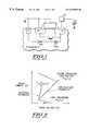
- FIG. 1illustrates, in partial schematic diagram form and partial cross-sectional view, an N-channel metal-oxide semiconductor (MOS) transistor and an inherent parasitic bipolar transistor in accordance with the prior art.
- MOSmetal-oxide semiconductor
- FIG. 1illustrates, an NPN bipolar device is formed in the p substrate having an emitter coupled to the source, a collector coupled to the drain, and a base coupled to the substrate of an N-channel MOS transistor.
- the substrate tie and the sourceare illustrated coupled to ground with the drain coupled to an I/O pad.
- the I/O padis shown receiving a positive ESD event.
- the parasitic bipolar deviceformed by an n+ diffusion coupled to the bondpad (collector) and an n+ diffusion coupled to ground (emitter), can conduct large amounts of ESD discharge current by means of a self-biased mechanism through the inherent substrate resistance labeled “Rsub”.
- the self-biasingresults from avalanche-breakdown at the collector/base (i.e. n+ pad to p-substrate) diffusion where avalanche-generated electron-hole pairs are created.
- the avalanche-generation sourceis shown schematically as current source I GEN in FIG. 1, which represents substrate (hole) current. The holes generated from this effect migrate towards the substrate tie through the inherent substrate resistance, thereby producing a local elevation in the substrate potential near the transistor.
- ballast resistorconnected between the drain of the N-channel MOS transistor and an output pin. This technique helps ensure some added measure of ESD protection in the event of bipolar conduction in the circuit by equally distributing any discharge current through the NMOS transistor (or several fingers forming a single NMOS transistor).
- the ballast resistoris added to ensure that the failure point at another collector-to-emitter voltage V T 2 , is greater than the collector-to-emitter voltage, V T 1 , where the current begins to flow in the parasitic bipolar transistor.
- V T 1 and V T 2is illustrated in FIG. 2 .
- FIG. 2illustrates a diagram of drain current versus drain voltage of the N-channel transistor of FIG. 1 .
- FIG. 2shows two curves. One curve illustrates drain current versus drain-to-source voltage for a typical non-salicided technology and the other curve illustrates drain current versus drain-to-source voltage for a typical salicided technology.
- NMOS transistorsor several fingers forming a single NMOS transistor
- V T 1collector-to-emitter voltage
- V T 2is usually greater than V T 1 since the on-resistance exhibited by the transistor is quite high (i.e. the slope of the line in FIG. 2 is less steep).
- V T 2is usually less than V T 1 , since the salicided source/drain diffusions act to lower the effective series resistance of the device (i.e.
- V T 2can be controlled to be greater than V T 1 by adding series resistance in the form of a ballast resistor. This guarantees that the first NMOS transistor (or finger of the NMOS transistor) does not break down at a voltage less than the voltage at which the second NMOS transistor turns on. This in turn guarantees that the failure current of the complete device is the sum total of its individual components rather than that of the first segment which snaps-back.
- the failure currentis the second breakdown current, I T 2 , shown in FIG. 2 .
- the value of I T 2must not be exceeded during an ESD event or else permanent damage will result in the device.
- the motivation for adding ballast resistanceis to maximize the total amount of I T 2 available from a given transistor.
- I T 2depends on specific fabrication parameters of a particular technology, and varies from technology to technology.
- FIG. 1illustrates, in partial schematic diagram form and partial cross-sectional view, an N-channel MOS transistor and an inherent parasitic bipolar transistor in accordance with the prior art.
- FIG. 2illustrates a diagram of drain current versus drain voltage of the N-channel MOS transistor of FIG. 1 .
- FIG. 3illustrates, in partial schematic diagram form and partial cross-sectional view, an ESD circuit in accordance with the present invention
- FIG. 4illustrates, in schematic diagram form, an ESD circuit in accordance with the present invention.
- the present inventioncommon to all embodiments lies in a circuit and method for raising the voltage of the source of the N-channel transistor in order to keep the base-emitter voltage of the parasitic bipolar device from forward biasing, to prevent conduction in the parasitic bipolar device.
- FIG. 3shows one embodiment where, a relatively small resistor ( 26 ) is coupled between the source of the N-channel transistor ( 24 ) and ground.
- a source injection current source ( 32 )is used to direct some of the ESD current from a positive ESD event through the small source resistor so that the source of the N-channel transistor is elevated during the event, thus preventing a forward biasing of the base-emitter junction which in-turn causes snapback of the inherent parasitic bipolar device.
- a positive potentialis produced by current flow through resistor 26 , at the cathode (n+ diffusion) of the diode formed between the source of transistor 24 and the p-type substrate (anode).
- this potentialcan easily be controlled by adjusting the value of resistor 26 or the relative strength of source injection current source 32 .
- the potential of the anode (substrate) of the diode formed by the n+ source diffusion of transistor 24is controlled by the avalanche-generation rate and effective substrate resistance, which in general, are difficult to engineer independently of other fabrication parameters.
- snapbackcan be controlled in a manner which does not alter or effect other physical or electrical parameters which are needed elsewhere in the fabrication process.
- FIG. 4illustrates, in schematic diagram form, an output buffer circuit 20 in accordance with the present invention.
- Output buffer circuit 20is an output buffer circuit having ESD protection, and includes P-channel transistor 22 , N-channel transistor 24 , resistor 26 , pad 30 , a source injection current source 32 which is further comprised of a source injection bias circuit 33 and a source injector transistor 34 , ESD rail clamp 46 , and diode 48 .
- P-channel transistor 22 and N-channel transistor 24together form an output buffer circuit.
- P-channel transistor 22is illustrated with its inherent diode 28 coupled between its drain and well.
- P-channel source injector transistor 34has a source coupled to pad 30 , a gate, and a drain coupled to one terminal of resistor 26 . The gate of P-channel source injector transistor 34 is biased by source injection bias circuit 33 .
- Source injection bias circuit 33includes P-channel transistors 36 and 38 , resistors 40 and 44 , and N-channel transistor 42 .
- P-channel transistor 36has a gate connected to VDD, a first source terminal connected to pad 30 , and a second drain terminal.
- P-channel transistor 38has a source connected to a positive power supply voltage terminal labeled VDD, a gate connected to ground, and a drain.
- Resistor 40has a first terminal connected to the drain of P-channel transistor 38 , and a second terminal.
- N-channel transistor 42has a drain connected to the second terminal of resistor 40 , a gate connected to the second drain terminal of P-channel channel transistor 36 , and a source connected to VSS.
- Resistor 44has a first terminal connected to the gate of N-channel transistor 42 , and a second terminal connected to a ground terminal labeled VSS.
- ESD rail clamp 46 and diode 48are coupled between VDD and VSS.
- ESD rail clamp 46may be the inherent capacitance of the integrated circuit incorporating circuit 20 , or may be an active clamp circuit used to provide a discharge path between VDD and VSS during an ESD event.
- Diode 48conducts current when VSS is about a diode voltage drop (V d ) above VDD.
- Source injection bias circuit 33places source injector transistor 34 into a non-conductive state to minimize current leakage.
- P-channel transistor 36will be substantially non-conductive, causing the voltage at the gate of N-channel transistor 42 to be low, and causing transistor 42 to be non-conductive. This in turn causes the voltage at the second terminal of resistor 40 to be high enough to cause P-channel source injector transistor 34 to be substantially non-conductive.
- source injection bias circuit 33maintains P-channel source injector transistor 34 in a conductive state.
- P-channel source injector transistor 34then functions as a current source.
- P-channel transistor 36becomes conductive when the voltage at pad 30 exceeds one threshold voltage drop above VDD, causing a relatively high voltage to be supplied to the gate of N-channel transistor 42 .
- N-channel transistor 42then becomes conductive causing the gate of P-channel transistor 34 to be pulled low, causing source injector P-channel transistor 34 to be conductive.
- Some of the ESD currentis conducted from pad 30 , through P-channel source injector transistor 34 and resistor 26 to VSS. The rest of the ESD event current flows through the inherent diode 28 of P-channel transistor 22 to VDD and then via ESD rail clamp 46 to VSS.
- the source voltage of N-channel transistor 24is increased, thus raising the emitter voltage of the inherent bipolar transistor (as illustrated in FIG. 1 and FIG. 3) preventing the inherent bipolar transistor from becoming conductive. This increases the pad voltage that can build up during an ESD event beyond that at which snapback would normally occur, which as discussed above, is particularly destructive to integrated circuits constructed using advanced, salicided technology.
- resistor 26The upper limit on the resistance of resistor 26 is determined by the length of turn-on delay caused by resistor 26 to N-channel transistor 24 . Only a small voltage on the source of N-channel transistor 24 is enough to prevent conduction of the parasitic bipolar device because the substrate potential cannot rise very high because the substrate is coupled to ground. The source of N-channel transistor 24 just needs to be a diode drop above the substrate to prevent bipolar snapback from occurring. In the illustrated embodiment, resistor 26 is implemented having a resistance value of about 10 ohms or less.
- the gate of P-channel source injector transistor 34can be connected directly to VDD. While this approach would still permit source injector transistor 34 to inject current into resistor 26 , the amount of current would decrease as VDD begins to rise sympathetically with the pad 30 . This causes the source-to-gate voltage of source injector transistor 34 to decrease in magnitude which de-biases the device.
- an advantage to using source injection bias circuit 33is that if VDD begins to move sympathetically with pad 30 , a source-to-gate voltage sufficient to keep P-channel source injector transistor 34 highly conductive is maintained because transistor 36 needs to supply only a very small current to resistor 44 to cause the voltage across resistor 44 to exceed the threshold voltage of N-channel transistor 42 .
- resistor 44can easily be adjusted so that N-channel transistor 42 stays conductive, insuring that the gate voltage of transistor 34 is low enough to cause P-channel source injector transistor 34 to remain highly conductive.
- resistor 26with the current source 32 formed by source injector transistor 34 and source injector bias circuit 33 can greatly extend the ESD range of the buffer circuit before breakdown occurs, which gives the ESD protection circuit more margin before failure of the device.
Landscapes
- Semiconductor Integrated Circuits (AREA)
- Metal-Oxide And Bipolar Metal-Oxide Semiconductor Integrated Circuits (AREA)
- Insulated Gate Type Field-Effect Transistor (AREA)
Abstract
Description
Claims (14)
Priority Applications (7)
| Application Number | Priority Date | Filing Date | Title |
|---|---|---|---|
| US09/201,392US6329692B1 (en) | 1998-11-30 | 1998-11-30 | Circuit and method for reducing parasitic bipolar effects during eletrostatic discharges |
| TW088119225ATW454306B (en) | 1998-11-30 | 1999-11-04 | Circuit and method for reducing parasitic bipolar effects during electrostatic discharges |
| CNB99120977XACN1167132C (en) | 1998-11-30 | 1999-11-29 | Circuit and method for reducing parasitic bipolar effect during electrostatic discharge |
| JP33849799AJP4401500B2 (en) | 1998-11-30 | 1999-11-29 | Semiconductor device and method for reducing parasitic bipolar effect in electrostatic discharge |
| KR1019990053752AKR100717973B1 (en) | 1998-11-30 | 1999-11-30 | Circuit and method for reducing parasitic bipolar effects during electrostatic discharges |
| US09/559,354US6373104B1 (en) | 1998-11-30 | 2000-04-27 | Circuit method for reducing parasitic bipolar effects during electrostatic discharges |
| US09/560,501US6284616B1 (en) | 1998-11-30 | 2000-04-27 | Circuit and method for reducing parasitic bipolar effects during electrostatic discharges |
Applications Claiming Priority (1)
| Application Number | Priority Date | Filing Date | Title |
|---|---|---|---|
| US09/201,392US6329692B1 (en) | 1998-11-30 | 1998-11-30 | Circuit and method for reducing parasitic bipolar effects during eletrostatic discharges |
Related Child Applications (2)
| Application Number | Title | Priority Date | Filing Date |
|---|---|---|---|
| US09/559,354Continuation-In-PartUS6373104B1 (en) | 1998-11-30 | 2000-04-27 | Circuit method for reducing parasitic bipolar effects during electrostatic discharges |
| US09/560,501DivisionUS6284616B1 (en) | 1998-11-30 | 2000-04-27 | Circuit and method for reducing parasitic bipolar effects during electrostatic discharges |
Publications (1)
| Publication Number | Publication Date |
|---|---|
| US6329692B1true US6329692B1 (en) | 2001-12-11 |
Family
ID=22745641
Family Applications (3)
| Application Number | Title | Priority Date | Filing Date |
|---|---|---|---|
| US09/201,392Expired - LifetimeUS6329692B1 (en) | 1998-11-30 | 1998-11-30 | Circuit and method for reducing parasitic bipolar effects during eletrostatic discharges |
| US09/559,354Expired - LifetimeUS6373104B1 (en) | 1998-11-30 | 2000-04-27 | Circuit method for reducing parasitic bipolar effects during electrostatic discharges |
| US09/560,501Expired - LifetimeUS6284616B1 (en) | 1998-11-30 | 2000-04-27 | Circuit and method for reducing parasitic bipolar effects during electrostatic discharges |
Family Applications After (2)
| Application Number | Title | Priority Date | Filing Date |
|---|---|---|---|
| US09/559,354Expired - LifetimeUS6373104B1 (en) | 1998-11-30 | 2000-04-27 | Circuit method for reducing parasitic bipolar effects during electrostatic discharges |
| US09/560,501Expired - LifetimeUS6284616B1 (en) | 1998-11-30 | 2000-04-27 | Circuit and method for reducing parasitic bipolar effects during electrostatic discharges |
Country Status (5)
| Country | Link |
|---|---|
| US (3) | US6329692B1 (en) |
| JP (1) | JP4401500B2 (en) |
| KR (1) | KR100717973B1 (en) |
| CN (1) | CN1167132C (en) |
| TW (1) | TW454306B (en) |
Cited By (14)
| Publication number | Priority date | Publication date | Assignee | Title |
|---|---|---|---|---|
| US6524898B2 (en)* | 1999-11-18 | 2003-02-25 | Oki Electric Industry Co., Ltd. | Method of fabricating a protective element in an SOI substrate |
| DE10201056A1 (en)* | 2002-01-14 | 2003-07-31 | Infineon Technologies Ag | Semiconductor device for operating with a safety transistor has a bipolar safety transistor with an emitter area to show voltage kickback. |
| US20040085093A1 (en)* | 2002-10-31 | 2004-05-06 | Micron Technology, Inc. | Methods, circuits, and applications using a resistor and a schottky diode |
| US20040141268A1 (en)* | 2003-01-22 | 2004-07-22 | Miller James W. | Electrostatic discharge circuit and method therefor |
| US20040141267A1 (en)* | 2003-01-22 | 2004-07-22 | Khazhinsky Michael G. | Electrostatic discharge circuit and method therefor |
| US20040155300A1 (en)* | 2003-02-10 | 2004-08-12 | Michael Baird | Low voltage NMOS-based electrostatic discharge clamp |
| US6809348B1 (en)* | 1999-10-08 | 2004-10-26 | Denso Corporation | Semiconductor device and method for manufacturing the same |
| US20050071789A1 (en)* | 2003-09-30 | 2005-03-31 | International Business Machines Corporation | Latch-up analysis and parameter modification |
| US20090070718A1 (en)* | 2003-11-19 | 2009-03-12 | International Business Machines Corporation | Methodology for placement based on circuit function and latchup sensitivity |
| US20110101425A1 (en)* | 2009-10-29 | 2011-05-05 | Freescale Semiconductor, Inc. | Semiconductor device with increased snapback voltage |
| US8000067B1 (en) | 2003-05-15 | 2011-08-16 | Marvell International Ltd. | Method and apparatus for improving supply noise rejection |
| US8338872B2 (en) | 2010-03-30 | 2012-12-25 | Freescale Semiconductor, Inc. | Electronic device with capcitively coupled floating buried layer |
| US8344472B2 (en) | 2010-03-30 | 2013-01-01 | Freescale Semiconductor, Inc. | Semiconductor device and method |
| US20150008581A1 (en)* | 2011-05-27 | 2015-01-08 | Taiwan Semiconductor Manufacturing Company, Ltd. | Package-on-Package Process for Applying Molding Compound |
Families Citing this family (25)
| Publication number | Priority date | Publication date | Assignee | Title |
|---|---|---|---|---|
| JP2002083931A (en)* | 2000-09-08 | 2002-03-22 | Nec Corp | Semiconductor integrated circuit device |
| JP2002305254A (en)* | 2001-04-05 | 2002-10-18 | Mitsubishi Electric Corp | Semiconductor device and manufacturing method thereof |
| US6650103B2 (en)* | 2001-05-31 | 2003-11-18 | Analog Devices, Inc. | Magnetic snapback sensor circuit and electrostatic discharge circuit using same |
| JP2003031669A (en)* | 2001-07-13 | 2003-01-31 | Ricoh Co Ltd | Semiconductor device |
| US7042689B2 (en)* | 2003-01-21 | 2006-05-09 | Taiwan Semiconductor Manufacturing Co., Ltd. | High voltage tolerant ESD design for analog and RF applications in deep submicron CMOS technologies |
| US7196887B2 (en)* | 2003-05-28 | 2007-03-27 | Texas Instruments Incorporated | PMOS electrostatic discharge (ESD) protection device |
| JP2005093696A (en)* | 2003-09-17 | 2005-04-07 | Matsushita Electric Ind Co Ltd | Horizontal MOS transistor |
| US7651306B2 (en) | 2004-12-22 | 2010-01-26 | Applied Materials, Inc. | Cartesian robot cluster tool architecture |
| US7798764B2 (en) | 2005-12-22 | 2010-09-21 | Applied Materials, Inc. | Substrate processing sequence in a cartesian robot cluster tool |
| US7819079B2 (en) | 2004-12-22 | 2010-10-26 | Applied Materials, Inc. | Cartesian cluster tool configuration for lithography type processes |
| US7255747B2 (en) | 2004-12-22 | 2007-08-14 | Sokudo Co., Ltd. | Coat/develop module with independent stations |
| TW200739872A (en)* | 2006-04-04 | 2007-10-16 | Univ Nat Chiao Tung | Power line electrostatic discharge protection circuit featuring triple voltage tolerance |
| TW200816878A (en)* | 2006-09-27 | 2008-04-01 | Silicon Motion Inc | Electrostatic discharge (ESD) protection device |
| US7672101B2 (en) | 2007-09-10 | 2010-03-02 | Taiwan Semiconductor Manufacturing Co., Ltd. | ESD protection circuit and method |
| CN101533830B (en)* | 2008-03-11 | 2012-05-09 | 义隆电子股份有限公司 | Electrostatic discharge protection device for high voltage pad |
| WO2010038101A1 (en)* | 2008-10-03 | 2010-04-08 | Freescale Semiconductor, Inc. | Semiconductor device and electronic device |
| US8693149B2 (en)* | 2009-05-20 | 2014-04-08 | Semiconductor Components Industries, Llc. | Transient suppression device and method therefor |
| US20110102046A1 (en)* | 2009-10-31 | 2011-05-05 | Pankaj Kumar | Interfacing between differing voltage level requirements in an integrated circuit system |
| CN102332403A (en)* | 2011-09-20 | 2012-01-25 | 中国科学院微电子研究所 | A kind of semiconductor structure and its manufacturing method |
| US10553633B2 (en)* | 2014-05-30 | 2020-02-04 | Klaus Y.J. Hsu | Phototransistor with body-strapped base |
| TWI521824B (en)* | 2014-08-08 | 2016-02-11 | 朋程科技股份有限公司 | Electrostatic discharge protection circuit and voltage regulator chip having the same |
| US10332871B2 (en)* | 2016-03-18 | 2019-06-25 | Intel IP Corporation | Area-efficient and robust electrostatic discharge circuit |
| US11316340B2 (en)* | 2019-07-30 | 2022-04-26 | Infineon Technologies Ag | Electrostatic discharge with parasitic compensation |
| US10840907B1 (en) | 2019-11-19 | 2020-11-17 | Honeywell International Inc. | Source-coupled logic with reference controlled inputs |
| US11329481B2 (en) | 2020-05-18 | 2022-05-10 | Littelfuse, Inc. | Current limiting circuit arrangement |
Citations (7)
| Publication number | Priority date | Publication date | Assignee | Title |
|---|---|---|---|---|
| US5019888A (en) | 1987-07-23 | 1991-05-28 | Texas Instruments Incorporated | Circuit to improve electrostatic discharge protection |
| US5021853A (en) | 1990-04-27 | 1991-06-04 | Digital Equipment Corporation | N-channel clamp for ESD protection in self-aligned silicided CMOS process |
| US5157573A (en) | 1989-05-12 | 1992-10-20 | Western Digital Corporation | ESD protection circuit with segmented buffer transistor |
| US5225702A (en) | 1991-12-05 | 1993-07-06 | Texas Instruments Incorporated | Silicon controlled rectifier structure for electrostatic discharge protection |
| US5440162A (en) | 1994-07-26 | 1995-08-08 | Rockwell International Corporation | ESD protection for submicron CMOS circuits |
| US5465189A (en) | 1990-03-05 | 1995-11-07 | Texas Instruments Incorporated | Low voltage triggering semiconductor controlled rectifiers |
| US5903419A (en) | 1997-09-29 | 1999-05-11 | Motorola, Inc. | Circuit for electrostatic discharge (ESD) protection |
Family Cites Families (6)
| Publication number | Priority date | Publication date | Assignee | Title |
|---|---|---|---|---|
| US5153529A (en)* | 1991-08-30 | 1992-10-06 | Motorola, Inc. | Rail-to-rail input stage of an operational amplifier |
| US5528193A (en)* | 1994-11-21 | 1996-06-18 | National Semiconductor Corporation | Circuit for generating accurate voltage levels below substrate voltage |
| US5534792A (en)* | 1995-02-15 | 1996-07-09 | Burr-Brown Corporation | Low capacitance electronically controlled active bus terminator circuit and method |
| US5798658A (en)* | 1995-06-15 | 1998-08-25 | Werking; Paul M. | Source-coupled logic with reference controlled inputs |
| KR100223923B1 (en)* | 1996-11-19 | 1999-10-15 | 구본준 | Static charge preventing apparatus |
| US6204715B1 (en)* | 1999-02-26 | 2001-03-20 | General Motors Corporation | Signal amplifying circuit |
- 1998
- 1998-11-30USUS09/201,392patent/US6329692B1/ennot_activeExpired - Lifetime
- 1999
- 1999-11-04TWTW088119225Apatent/TW454306B/ennot_activeIP Right Cessation
- 1999-11-29JPJP33849799Apatent/JP4401500B2/ennot_activeExpired - Fee Related
- 1999-11-29CNCNB99120977XApatent/CN1167132C/ennot_activeExpired - Lifetime
- 1999-11-30KRKR1019990053752Apatent/KR100717973B1/ennot_activeExpired - Lifetime
- 2000
- 2000-04-27USUS09/559,354patent/US6373104B1/ennot_activeExpired - Lifetime
- 2000-04-27USUS09/560,501patent/US6284616B1/ennot_activeExpired - Lifetime
Patent Citations (7)
| Publication number | Priority date | Publication date | Assignee | Title |
|---|---|---|---|---|
| US5019888A (en) | 1987-07-23 | 1991-05-28 | Texas Instruments Incorporated | Circuit to improve electrostatic discharge protection |
| US5157573A (en) | 1989-05-12 | 1992-10-20 | Western Digital Corporation | ESD protection circuit with segmented buffer transistor |
| US5465189A (en) | 1990-03-05 | 1995-11-07 | Texas Instruments Incorporated | Low voltage triggering semiconductor controlled rectifiers |
| US5021853A (en) | 1990-04-27 | 1991-06-04 | Digital Equipment Corporation | N-channel clamp for ESD protection in self-aligned silicided CMOS process |
| US5225702A (en) | 1991-12-05 | 1993-07-06 | Texas Instruments Incorporated | Silicon controlled rectifier structure for electrostatic discharge protection |
| US5440162A (en) | 1994-07-26 | 1995-08-08 | Rockwell International Corporation | ESD protection for submicron CMOS circuits |
| US5903419A (en) | 1997-09-29 | 1999-05-11 | Motorola, Inc. | Circuit for electrostatic discharge (ESD) protection |
Non-Patent Citations (4)
| Title |
|---|
| "A Substrate Triggered Lateral Bipolar Circuit for High Voltage Tolerant ESD Protection Applications," Smith. |
| "Analysis of Snubber-Clamped Diode-String Mixed Voltage Interface ESD Protection Network for Advanced Microprocessors," Voldman et al.;EOS/ESD Symposium 95; pp. 43-61. |
| "EOS/ESD Analysis of High-Density Logic Chips," Ramaswamy, et al; EOS/ESD Symposium 96; pp. 286-290. |
| "Substrate Triggering and Salicide Effects on ESD Performances and Protection Circuit Design in Deep Submicron CMOS Process," Amerasekera, et al; IEDM 95; pp. 575-550. |
Cited By (32)
| Publication number | Priority date | Publication date | Assignee | Title |
|---|---|---|---|---|
| US6809348B1 (en)* | 1999-10-08 | 2004-10-26 | Denso Corporation | Semiconductor device and method for manufacturing the same |
| US6784497B2 (en) | 1999-11-18 | 2004-08-31 | Oki Electric Industry, Co., Ltd. | Semiconductor device |
| US20030104660A1 (en)* | 1999-11-18 | 2003-06-05 | Oki Electric Industry Co., Ltd. | Semiconductor device |
| US6524898B2 (en)* | 1999-11-18 | 2003-02-25 | Oki Electric Industry Co., Ltd. | Method of fabricating a protective element in an SOI substrate |
| DE10201056A1 (en)* | 2002-01-14 | 2003-07-31 | Infineon Technologies Ag | Semiconductor device for operating with a safety transistor has a bipolar safety transistor with an emitter area to show voltage kickback. |
| DE10201056B4 (en)* | 2002-01-14 | 2007-06-21 | Infineon Technologies Ag | Semiconductor device with a bipolar protection transistor |
| US7075763B2 (en)* | 2002-10-31 | 2006-07-11 | Micron Technology, Inc. | Methods, circuits, and applications using a resistor and a Schottky diode |
| US20060198070A1 (en)* | 2002-10-31 | 2006-09-07 | Micron Technology, Inc. | Methods, circuits, and applications using a resistor and a Schottky diode |
| US7369379B2 (en) | 2002-10-31 | 2008-05-06 | Micron Technology, Inc. | Methods, circuits, and applications using a resistor and a Schottky diode |
| US20040085093A1 (en)* | 2002-10-31 | 2004-05-06 | Micron Technology, Inc. | Methods, circuits, and applications using a resistor and a schottky diode |
| US7236339B2 (en) | 2003-01-22 | 2007-06-26 | Freescale Semiconductor, Inc. | Electrostatic discharge circuit and method therefor |
| US20040141267A1 (en)* | 2003-01-22 | 2004-07-22 | Khazhinsky Michael G. | Electrostatic discharge circuit and method therefor |
| US6879476B2 (en) | 2003-01-22 | 2005-04-12 | Freescale Semiconductor, Inc. | Electrostatic discharge circuit and method therefor |
| US6900970B2 (en) | 2003-01-22 | 2005-05-31 | Freescale Semiconductor, Inc. | Electrostatic discharge circuit and method therefor |
| US20050185351A1 (en)* | 2003-01-22 | 2005-08-25 | Miller James W. | Electrostatic discharge circuit and method therefor |
| US20040141268A1 (en)* | 2003-01-22 | 2004-07-22 | Miller James W. | Electrostatic discharge circuit and method therefor |
| US6844597B2 (en)* | 2003-02-10 | 2005-01-18 | Freescale Semiconductor, Inc. | Low voltage NMOS-based electrostatic discharge clamp |
| WO2004073023A3 (en)* | 2003-02-10 | 2004-12-23 | Freescale Semiconductor Inc | Low voltage nmos-based electrostatic discharge clamp |
| US20040155300A1 (en)* | 2003-02-10 | 2004-08-12 | Michael Baird | Low voltage NMOS-based electrostatic discharge clamp |
| US7288820B2 (en) | 2003-02-10 | 2007-10-30 | Freescale Semiconductor, Inc. | Low voltage NMOS-based electrostatic discharge clamp |
| KR101006827B1 (en) | 2003-02-10 | 2011-01-12 | 프리스케일 세미컨덕터, 인크. | Low Voltage NMOS-based Electrostatic Discharge Clamp |
| US8000067B1 (en) | 2003-05-15 | 2011-08-16 | Marvell International Ltd. | Method and apparatus for improving supply noise rejection |
| US20050071789A1 (en)* | 2003-09-30 | 2005-03-31 | International Business Machines Corporation | Latch-up analysis and parameter modification |
| US6996786B2 (en)* | 2003-09-30 | 2006-02-07 | International Business Machines Corporation | Latch-up analysis and parameter modification |
| US8108822B2 (en)* | 2003-11-19 | 2012-01-31 | International Business Machines Corporation | Methodology for placement based on circuit function and latchup sensitivity |
| US20090070718A1 (en)* | 2003-11-19 | 2009-03-12 | International Business Machines Corporation | Methodology for placement based on circuit function and latchup sensitivity |
| US20110101425A1 (en)* | 2009-10-29 | 2011-05-05 | Freescale Semiconductor, Inc. | Semiconductor device with increased snapback voltage |
| US8193585B2 (en) | 2009-10-29 | 2012-06-05 | Freescale Semiconductor, Inc. | Semiconductor device with increased snapback voltage |
| US8338872B2 (en) | 2010-03-30 | 2012-12-25 | Freescale Semiconductor, Inc. | Electronic device with capcitively coupled floating buried layer |
| US8344472B2 (en) | 2010-03-30 | 2013-01-01 | Freescale Semiconductor, Inc. | Semiconductor device and method |
| US20150008581A1 (en)* | 2011-05-27 | 2015-01-08 | Taiwan Semiconductor Manufacturing Company, Ltd. | Package-on-Package Process for Applying Molding Compound |
| US10134703B2 (en)* | 2011-05-27 | 2018-11-20 | Taiwan Semiconductor Manufacturing Company, Ltd. | Package on-package process for applying molding compound |
Also Published As
| Publication number | Publication date |
|---|---|
| JP4401500B2 (en) | 2010-01-20 |
| KR20000035771A (en) | 2000-06-26 |
| US6373104B1 (en) | 2002-04-16 |
| US6284616B1 (en) | 2001-09-04 |
| CN1167132C (en) | 2004-09-15 |
| JP2000174133A (en) | 2000-06-23 |
| KR100717973B1 (en) | 2007-05-16 |
| CN1256516A (en) | 2000-06-14 |
| TW454306B (en) | 2001-09-11 |
Similar Documents
| Publication | Publication Date | Title |
|---|---|---|
| US6329692B1 (en) | Circuit and method for reducing parasitic bipolar effects during eletrostatic discharges | |
| US11315919B2 (en) | Circuit for controlling a stacked snapback clamp | |
| US6900970B2 (en) | Electrostatic discharge circuit and method therefor | |
| US6049119A (en) | Protection circuit for a semiconductor device | |
| US6479872B1 (en) | Dynamic substrate-coupled electrostatic discharging protection circuit | |
| US7728349B2 (en) | Low capacitance SCR with trigger element | |
| US9029910B2 (en) | Programmable SCR for ESD protection | |
| US6433979B1 (en) | Electrostatic discharge protection device using semiconductor controlled rectifier | |
| US20070194380A1 (en) | Method for fabricating an ESD protection apparatus for discharging electric charge in a depth direction | |
| JP2008524857A (en) | Device having a low voltage trigger element | |
| US6569740B1 (en) | Method of forming a semiconductor device having a buffer | |
| US6879476B2 (en) | Electrostatic discharge circuit and method therefor | |
| KR19980071441A (en) | Electrostatic Discharge Protection Circuit | |
| CN110085583B (en) | Semiconductor device and operating method | |
| KR20040090480A (en) | Semiconductor device having protection circuit for protecting internal circuit | |
| KR100435807B1 (en) | Semiconductor controlled rectifier for use in electrostatic discharge protecting circuit | |
| KR100504203B1 (en) | Protecting device of semiconductor device | |
| JPH044755B2 (en) | ||
| US6784499B2 (en) | Semiconductor device serving as a protecting element | |
| KR0165384B1 (en) | Static electricity protection structure of semiconductor device |
Legal Events
| Date | Code | Title | Description |
|---|---|---|---|
| AS | Assignment | Owner name:MOTOROLA, INC., ILLINOIS Free format text:ASSIGNMENT OF ASSIGNORS INTEREST;ASSIGNOR:SMITH, JEREMY C.;REEL/FRAME:009620/0936 Effective date:19981125 | |
| STCF | Information on status: patent grant | Free format text:PATENTED CASE | |
| AS | Assignment | Owner name:FREESCALE SEMICONDUCTOR, INC., TEXAS Free format text:ASSIGNMENT OF ASSIGNORS INTEREST;ASSIGNOR:MOTOROLA, INC.;REEL/FRAME:015698/0657 Effective date:20040404 Owner name:FREESCALE SEMICONDUCTOR, INC.,TEXAS Free format text:ASSIGNMENT OF ASSIGNORS INTEREST;ASSIGNOR:MOTOROLA, INC.;REEL/FRAME:015698/0657 Effective date:20040404 | |
| FPAY | Fee payment | Year of fee payment:4 | |
| AS | Assignment | Owner name:CITIBANK, N.A. AS COLLATERAL AGENT, NEW YORK Free format text:SECURITY AGREEMENT;ASSIGNORS:FREESCALE SEMICONDUCTOR, INC.;FREESCALE ACQUISITION CORPORATION;FREESCALE ACQUISITION HOLDINGS CORP.;AND OTHERS;REEL/FRAME:018855/0129 Effective date:20061201 Owner name:CITIBANK, N.A. AS COLLATERAL AGENT,NEW YORK Free format text:SECURITY AGREEMENT;ASSIGNORS:FREESCALE SEMICONDUCTOR, INC.;FREESCALE ACQUISITION CORPORATION;FREESCALE ACQUISITION HOLDINGS CORP.;AND OTHERS;REEL/FRAME:018855/0129 Effective date:20061201 | |
| FPAY | Fee payment | Year of fee payment:8 | |
| AS | Assignment | Owner name:CITIBANK, N.A., AS COLLATERAL AGENT,NEW YORK Free format text:SECURITY AGREEMENT;ASSIGNOR:FREESCALE SEMICONDUCTOR, INC.;REEL/FRAME:024397/0001 Effective date:20100413 Owner name:CITIBANK, N.A., AS COLLATERAL AGENT, NEW YORK Free format text:SECURITY AGREEMENT;ASSIGNOR:FREESCALE SEMICONDUCTOR, INC.;REEL/FRAME:024397/0001 Effective date:20100413 | |
| FPAY | Fee payment | Year of fee payment:12 | |
| AS | Assignment | Owner name:CITIBANK, N.A., AS NOTES COLLATERAL AGENT, NEW YORK Free format text:SECURITY AGREEMENT;ASSIGNOR:FREESCALE SEMICONDUCTOR, INC.;REEL/FRAME:030633/0424 Effective date:20130521 Owner name:CITIBANK, N.A., AS NOTES COLLATERAL AGENT, NEW YOR Free format text:SECURITY AGREEMENT;ASSIGNOR:FREESCALE SEMICONDUCTOR, INC.;REEL/FRAME:030633/0424 Effective date:20130521 | |
| AS | Assignment | Owner name:CITIBANK, N.A., AS NOTES COLLATERAL AGENT, NEW YORK Free format text:SECURITY AGREEMENT;ASSIGNOR:FREESCALE SEMICONDUCTOR, INC.;REEL/FRAME:031591/0266 Effective date:20131101 Owner name:CITIBANK, N.A., AS NOTES COLLATERAL AGENT, NEW YOR Free format text:SECURITY AGREEMENT;ASSIGNOR:FREESCALE SEMICONDUCTOR, INC.;REEL/FRAME:031591/0266 Effective date:20131101 | |
| AS | Assignment | Owner name:FREESCALE SEMICONDUCTOR, INC., TEXAS Free format text:PATENT RELEASE;ASSIGNOR:CITIBANK, N.A., AS COLLATERAL AGENT;REEL/FRAME:037356/0553 Effective date:20151207 Owner name:FREESCALE SEMICONDUCTOR, INC., TEXAS Free format text:PATENT RELEASE;ASSIGNOR:CITIBANK, N.A., AS COLLATERAL AGENT;REEL/FRAME:037356/0143 Effective date:20151207 Owner name:FREESCALE SEMICONDUCTOR, INC., TEXAS Free format text:PATENT RELEASE;ASSIGNOR:CITIBANK, N.A., AS COLLATERAL AGENT;REEL/FRAME:037354/0225 Effective date:20151207 | |
| AS | Assignment | Owner name:MORGAN STANLEY SENIOR FUNDING, INC., MARYLAND Free format text:ASSIGNMENT AND ASSUMPTION OF SECURITY INTEREST IN PATENTS;ASSIGNOR:CITIBANK, N.A.;REEL/FRAME:037486/0517 Effective date:20151207 | |
| AS | Assignment | Owner name:MORGAN STANLEY SENIOR FUNDING, INC., MARYLAND Free format text:ASSIGNMENT AND ASSUMPTION OF SECURITY INTEREST IN PATENTS;ASSIGNOR:CITIBANK, N.A.;REEL/FRAME:037518/0292 Effective date:20151207 | |
| AS | Assignment | Owner name:MORGAN STANLEY SENIOR FUNDING, INC., MARYLAND Free format text:SUPPLEMENT TO THE SECURITY AGREEMENT;ASSIGNOR:FREESCALE SEMICONDUCTOR, INC.;REEL/FRAME:039138/0001 Effective date:20160525 | |
| AS | Assignment | Owner name:NXP, B.V., F/K/A FREESCALE SEMICONDUCTOR, INC., NETHERLANDS Free format text:RELEASE BY SECURED PARTY;ASSIGNOR:MORGAN STANLEY SENIOR FUNDING, INC.;REEL/FRAME:040925/0001 Effective date:20160912 Owner name:NXP, B.V., F/K/A FREESCALE SEMICONDUCTOR, INC., NE Free format text:RELEASE BY SECURED PARTY;ASSIGNOR:MORGAN STANLEY SENIOR FUNDING, INC.;REEL/FRAME:040925/0001 Effective date:20160912 | |
| AS | Assignment | Owner name:NXP B.V., NETHERLANDS Free format text:RELEASE BY SECURED PARTY;ASSIGNOR:MORGAN STANLEY SENIOR FUNDING, INC.;REEL/FRAME:040928/0001 Effective date:20160622 | |
| AS | Assignment | Owner name:NXP USA, INC., TEXAS Free format text:CHANGE OF NAME;ASSIGNOR:FREESCALE SEMICONDUCTOR INC.;REEL/FRAME:040652/0180 Effective date:20161107 | |
| AS | Assignment | Owner name:NXP USA, INC., TEXAS Free format text:CORRECTIVE ASSIGNMENT TO CORRECT THE NATURE OF CONVEYANCE LISTED CHANGE OF NAME SHOULD BE MERGER AND CHANGE PREVIOUSLY RECORDED AT REEL: 040652 FRAME: 0180. ASSIGNOR(S) HEREBY CONFIRMS THE MERGER AND CHANGE OF NAME;ASSIGNOR:FREESCALE SEMICONDUCTOR INC.;REEL/FRAME:041354/0148 Effective date:20161107 | |
| AS | Assignment | Owner name:MORGAN STANLEY SENIOR FUNDING, INC., MARYLAND Free format text:CORRECTIVE ASSIGNMENT TO CORRECT THE REMOVE PATENTS 8108266 AND 8062324 AND REPLACE THEM WITH 6108266 AND 8060324 PREVIOUSLY RECORDED ON REEL 037518 FRAME 0292. ASSIGNOR(S) HEREBY CONFIRMS THE ASSIGNMENT AND ASSUMPTION OF SECURITY INTEREST IN PATENTS;ASSIGNOR:CITIBANK, N.A.;REEL/FRAME:041703/0536 Effective date:20151207 | |
| AS | Assignment | Owner name:SHENZHEN XINGUODU TECHNOLOGY CO., LTD., CHINA Free format text:CORRECTIVE ASSIGNMENT TO CORRECT THE TO CORRECT THE APPLICATION NO. FROM 13,883,290 TO 13,833,290 PREVIOUSLY RECORDED ON REEL 041703 FRAME 0536. ASSIGNOR(S) HEREBY CONFIRMS THE THE ASSIGNMENT AND ASSUMPTION OF SECURITYINTEREST IN PATENTS.;ASSIGNOR:MORGAN STANLEY SENIOR FUNDING, INC.;REEL/FRAME:048734/0001 Effective date:20190217 | |
| AS | Assignment | Owner name:NXP B.V., NETHERLANDS Free format text:RELEASE BY SECURED PARTY;ASSIGNOR:MORGAN STANLEY SENIOR FUNDING, INC.;REEL/FRAME:050744/0097 Effective date:20190903 | |
| AS | Assignment | Owner name:MORGAN STANLEY SENIOR FUNDING, INC., MARYLAND Free format text:CORRECTIVE ASSIGNMENT TO CORRECT THE REMOVE APPLICATION11759915 AND REPLACE IT WITH APPLICATION 11759935 PREVIOUSLY RECORDED ON REEL 037486 FRAME 0517. ASSIGNOR(S) HEREBY CONFIRMS THE ASSIGNMENT AND ASSUMPTION OF SECURITYINTEREST IN PATENTS;ASSIGNOR:CITIBANK, N.A.;REEL/FRAME:053547/0421 Effective date:20151207 | |
| AS | Assignment | Owner name:NXP B.V., NETHERLANDS Free format text:CORRECTIVE ASSIGNMENT TO CORRECT THE REMOVEAPPLICATION 11759915 AND REPLACE IT WITH APPLICATION11759935 PREVIOUSLY RECORDED ON REEL 040928 FRAME 0001. ASSIGNOR(S) HEREBY CONFIRMS THE RELEASE OF SECURITYINTEREST;ASSIGNOR:MORGAN STANLEY SENIOR FUNDING, INC.;REEL/FRAME:052915/0001 Effective date:20160622 | |
| AS | Assignment | Owner name:NXP, B.V. F/K/A FREESCALE SEMICONDUCTOR, INC., NETHERLANDS Free format text:CORRECTIVE ASSIGNMENT TO CORRECT THE REMOVEAPPLICATION 11759915 AND REPLACE IT WITH APPLICATION11759935 PREVIOUSLY RECORDED ON REEL 040925 FRAME 0001. ASSIGNOR(S) HEREBY CONFIRMS THE RELEASE OF SECURITYINTEREST;ASSIGNOR:MORGAN STANLEY SENIOR FUNDING, INC.;REEL/FRAME:052917/0001 Effective date:20160912 |