US6329266B1 - Methods of forming isolation trenches including damaging a trench isolation mask - Google Patents
Methods of forming isolation trenches including damaging a trench isolation maskDownload PDFInfo
- Publication number
- US6329266B1 US6329266B1US09/323,500US32350099AUS6329266B1US 6329266 B1US6329266 B1US 6329266B1US 32350099 AUS32350099 AUS 32350099AUS 6329266 B1US6329266 B1US 6329266B1
- Authority
- US
- United States
- Prior art keywords
- trench
- layer
- mask layer
- forming
- isolation
- Prior art date
- Legal status (The legal status is an assumption and is not a legal conclusion. Google has not performed a legal analysis and makes no representation as to the accuracy of the status listed.)
- Expired - Fee Related
Links
Images

Classifications
- H—ELECTRICITY
- H01—ELECTRIC ELEMENTS
- H01L—SEMICONDUCTOR DEVICES NOT COVERED BY CLASS H10
- H01L21/00—Processes or apparatus adapted for the manufacture or treatment of semiconductor or solid state devices or of parts thereof
- H01L21/70—Manufacture or treatment of devices consisting of a plurality of solid state components formed in or on a common substrate or of parts thereof; Manufacture of integrated circuit devices or of parts thereof
- H01L21/71—Manufacture of specific parts of devices defined in group H01L21/70
- H01L21/76—Making of isolation regions between components
- H01L21/762—Dielectric regions, e.g. EPIC dielectric isolation, LOCOS; Trench refilling techniques, SOI technology, use of channel stoppers
- H01L21/76224—Dielectric regions, e.g. EPIC dielectric isolation, LOCOS; Trench refilling techniques, SOI technology, use of channel stoppers using trench refilling with dielectric materials
- H—ELECTRICITY
- H01—ELECTRIC ELEMENTS
- H01L—SEMICONDUCTOR DEVICES NOT COVERED BY CLASS H10
- H01L21/00—Processes or apparatus adapted for the manufacture or treatment of semiconductor or solid state devices or of parts thereof
- H01L21/70—Manufacture or treatment of devices consisting of a plurality of solid state components formed in or on a common substrate or of parts thereof; Manufacture of integrated circuit devices or of parts thereof
- H01L21/71—Manufacture of specific parts of devices defined in group H01L21/70
- H01L21/76—Making of isolation regions between components
Definitions
- the present inventionrelates to the field of integrated circuits and more particularly to methods of forming isolation trenches for integrated circuit devices.
- DRAMDynamic Random Access Memory
- LOCOSlocal oxidation of silicon
- STIshallow trench isolation
- a nitride linerhas been used as an oxidation masking layer to reduce subsequent oxidation of the trench inner wall.
- the shallow pitcan be reduced.
- the nitride linermay be etched to a point below a surface of the semiconductor substrate (i.e., the nitride liner may be dented) during etching of an active nitride masking layer when using phosphoric acid.
- the dented nitride linermay cause a stringer residue in the subsequent step of etching a gate poly.
- the method mentioned aboveincludes the steps of: depositing a protective (masking) layer containing at least one layer of nitride on the semiconductor substrate; etching through the protective layer to form a set of isolation mask apertures; etching through the set of isolation mask apertures to form a set of isolation trenches; depositing a conformal liner of nitride having a thickness less than 50 ⁇ ; depositing a CVD layer of oxide having a thickness sufficient to fill the set of isolation trenches; removing the portion of the CVD layer of oxide outside the set of isolation trenches to expose the at least one layer of nitride; and stripping the at least one layer of nitride in phosphoric acid.
- the denting of the conformal nitride linermay be reduced by using a very thin nitride liner as an oxidation masking layer.
- the conformal nitride linermay be so thin that it is insufficient to prevent oxidation of the trench inner wall.
- an object of the present inventionto provide improved methods of forming isolation trenches.
- a trench mask layeron a surface of a semiconductor substrate wherein a portion of the semiconductor substrate is exposed through the trench mask layer, and forming an isolation trench in the exposed portion of the semiconductor substrate.
- a nitride lineris formed on surfaces of the isolation trench, a trench isolation layer is formed on the nitride liner wherein the trench isolation layer fills the trench, and the trench mask layer is damaged.
- the damaged trench mask layeris then stripped so that the surface of the semiconductor substrate is exposed.
- the trench mask layercan include a nitride trench mask layer and the step of damaging the trench mask layer can include damaging the nitride trench mask layer thereby weakening Si—N bonds of the nitride trench mask layer.
- the step of damaging the trench mask layercan include implanting ions into the trench mask layer.
- ions selected from the group of phosphorus (P), arsenic (As), boron (B), argon (Ar), and silicon (Si)can be implanted at a dose in the range of approximately 1 ⁇ 10 10 cm ⁇ 2 to approximately 1 ⁇ 10 17 cm ⁇ 2 , at an acceleration energy in the range of approximately 10 keV to approximately 1000 keV.
- the step of damaging the trench mask layercan include plasma treating the trench mask layer.
- the plasma treatmentcan be performed using an element selected from the group of xenon (Xe), krypton (Kr), and argon (Ar) at a power in the range of approximately 10 W to approximately 5000 W at a pressure in the range of approximately 1 ⁇ 10 4 Torr to approximately 700 Torr.
- the step of forming the trench mask layercan include forming a pad oxide layer on the surface of the substrate, forming a nitride layer on the pad oxide layer opposite the substrate, and patterning the pad oxide and nitride layers to provide the trench mask layer.
- the step of forming the isolation trenchcan include etching the exposed portion of the substrate.
- the step of forming the nitride linermay be preceded by the step of forming an oxide layer on the surfaces of the isolation trench. The formation of the oxide layer can reduce crystal damage in the substrate resulting from the etching of the trench.
- denting of the nitride linercan be reduced by damaging the trench mask layer before stripping the trench mask layer. Accordingly, isolation characteristics of the isolation trench can be improved. In addition, the time needed to strip the trench mask layer can be reduced.
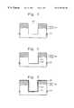
- FIGS. 1-7are cross sectional views illustrating steps of a method of forming isolation trenches according to the present invention.
- FIGS. 1-7are cross-sectional views illustrating steps of a method of forming an isolation trench according to the present invention.
- a pad oxide layer 202 a and an active nitride layer 202 bare sequentially formed on a semiconductor substrate 200 to provide a trench mask layer 202 .
- the trench mask layer 202is patterned using known photolithographic techniques to expose portions of the semiconductor substrate 200 .
- the semiconductor substrate 200is etched using the trench mask layer 202 as an etch mask to form a trench 203 .
- an oxide layer 204is formed on the bottom surface and both sidewalls of the trench 203 to reduce defects in silicon lattices caused by etching the semiconductor substrate 200 .
- the oxide layer 204can be, for example, a silicon dioxide (SiO 2 ) layer.
- an oxidation masking layersuch as a nitride liner 205 is formed on the active nitride layer 202 b of the trench mask layer 202 and on the oxide layer 204 in the trench 203 using an LPCVD technique to reduce subsequent oxidation of the trench inner wall.
- the nitride liner 205can be, for example, a silicon nitride (Si 3 N 4 ) layer.
- the nitride liner 205can be formed to have a thickness in the range of approximately 300 ⁇ to approximately 600 ⁇ sufficient to reduce subsequent oxidation.
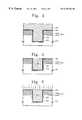
- a trench isolation layer 206(for example, a USG (O 3 TEOS) layer) is deposited to fill the trench 203 . Thereafter, an annealing step is performed to densify the trench isolation layer 206 . Referring to FIG. 5, the trench isolation layer 206 is removed until upper surfaces of the nitride liner 205 are exposed by using planarization-etching, for example, a CMP process.
- planarization-etchingfor example, a CMP process.
- an ion implantation or plasma treatmentis performed to weaken the Si—N bonding force of the active nitride layer 202 b without significantly damaging the semiconductor substrate 200 . Due to this ion implantation or plasma treatment, the time needed to strip the active nitride layer 202 b can be reduced.
- the above-mentioned ion implantationcan be carried out by implanting ions selected from the group consisting of P, As, B, Ar, and Si with a dose in the range of approximately 1 ⁇ 10 10 cm ⁇ 2 to approximately 1 ⁇ 10 17 cm ⁇ 2 , and with an acceleration energy in the range of approximately 10 keV to approximately 1000 keV.
- the above-mentioned plasma treatmentcan be carried out using ions selected from the group consisting of Xe, Kr, and Ar with a power in the range of approximately 10 W to approximately 5000 W, and a pressure in the range of approximately 1 ⁇ 10 ⁇ 4 Torr to approximately 700 Torr.
- the trench isolation 208is formed by etching the trench mask layer 202 b using phosphoric acid until the pad oxide layer 200 a is exposed.
- the active nitride layer of the trench mask layeris damaged before stripping the trench mask layer.
- the active nitride layercan be damaged using an ion implantation or a plasma treatment.
- the stripping time of the active nitride layer (and thus the trench mask layer)can thereby be reduced.
- the ion implantation of the plasma treatmentcan weaken the Si—N bond force in the active nitride layer. Accordingly, denting of the nitride liner in the trench can be reduced, and the isolation characteristics of the trench can be improved.
Landscapes
- Engineering & Computer Science (AREA)
- Physics & Mathematics (AREA)
- Condensed Matter Physics & Semiconductors (AREA)
- General Physics & Mathematics (AREA)
- Manufacturing & Machinery (AREA)
- Computer Hardware Design (AREA)
- Microelectronics & Electronic Packaging (AREA)
- Power Engineering (AREA)
- Element Separation (AREA)
- Formation Of Insulating Films (AREA)
Abstract
Description
The present invention relates to the field of integrated circuits and more particularly to methods of forming isolation trenches for integrated circuit devices.
As Dynamic Random Access Memory (DRAM) devices have become more highly integrated, device isolation methods have changed from the conventional LOCOS (local oxidation of silicon) technique to the STI (shallow trench isolation) technique. In case of the STI techniques, however, expansion of the oxide layer in the trench inner walls may cause a shallow pit in an active region. As a result, leakage currents may increase in the active region of a semiconductor substrate.
To reduce the above-mentioned problem, a nitride liner has been used as an oxidation masking layer to reduce subsequent oxidation of the trench inner wall. With the use of the nitride liner, the shallow pit can be reduced. The nitride liner, however, may be etched to a point below a surface of the semiconductor substrate (i.e., the nitride liner may be dented) during etching of an active nitride masking layer when using phosphoric acid. Thus, the dented nitride liner may cause a stringer residue in the subsequent step of etching a gate poly.
To reduce the described problems, a shallow isolation trench with a nitride liner having a thickness of less than 50 Å has been proposed. See, for example, U.S. Pat. No. 5,447,884, the disclosure of which is hereby incorporated herein in its entirety by reference.
The method mentioned above includes the steps of: depositing a protective (masking) layer containing at least one layer of nitride on the semiconductor substrate; etching through the protective layer to form a set of isolation mask apertures; etching through the set of isolation mask apertures to form a set of isolation trenches; depositing a conformal liner of nitride having a thickness less than 50 Å; depositing a CVD layer of oxide having a thickness sufficient to fill the set of isolation trenches; removing the portion of the CVD layer of oxide outside the set of isolation trenches to expose the at least one layer of nitride; and stripping the at least one layer of nitride in phosphoric acid. According to above method, the denting of the conformal nitride liner may be reduced by using a very thin nitride liner as an oxidation masking layer. The conformal nitride liner, however, may be so thin that it is insufficient to prevent oxidation of the trench inner wall.
Therefore, a method is needed which not only reduces denting the nitride liner but also reduces oxidation of the interior walls of the trench.
It is, therefore, an object of the present invention to provide improved methods of forming isolation trenches.
This and other objects are provided according to the present invention by forming a trench mask layer on a surface of a semiconductor substrate wherein a portion of the semiconductor substrate is exposed through the trench mask layer, and forming an isolation trench in the exposed portion of the semiconductor substrate. A nitride liner is formed on surfaces of the isolation trench, a trench isolation layer is formed on the nitride liner wherein the trench isolation layer fills the trench, and the trench mask layer is damaged. The damaged trench mask layer is then stripped so that the surface of the semiconductor substrate is exposed. By damaging the trench mask layer before stripping the trench mask layer, the time needed to strip the trench mask layer can be reduced, and damage to the nitride liner can be reduced. Accordingly, the isolation characteristics of the isolation trench can be improved.
In particular, the trench mask layer can include a nitride trench mask layer and the step of damaging the trench mask layer can include damaging the nitride trench mask layer thereby weakening Si—N bonds of the nitride trench mask layer. More particularly, the step of damaging the trench mask layer can include implanting ions into the trench mask layer. For example, ions selected from the group of phosphorus (P), arsenic (As), boron (B), argon (Ar), and silicon (Si) can be implanted at a dose in the range of approximately 1×1010cm−2to approximately 1×1017cm−2, at an acceleration energy in the range of approximately 10 keV to approximately 1000 keV.
Alternately, the step of damaging the trench mask layer can include plasma treating the trench mask layer. For example, the plasma treatment can be performed using an element selected from the group of xenon (Xe), krypton (Kr), and argon (Ar) at a power in the range of approximately 10 W to approximately 5000 W at a pressure in the range of approximately 1×10⁴Torr to approximately 700 Torr.
In addition, the step of forming the trench mask layer can include forming a pad oxide layer on the surface of the substrate, forming a nitride layer on the pad oxide layer opposite the substrate, and patterning the pad oxide and nitride layers to provide the trench mask layer. Moreover, the step of forming the isolation trench can include etching the exposed portion of the substrate. Furthermore, the step of forming the nitride liner may be preceded by the step of forming an oxide layer on the surfaces of the isolation trench. The formation of the oxide layer can reduce crystal damage in the substrate resulting from the etching of the trench.
According to the present invention, denting of the nitride liner can be reduced by damaging the trench mask layer before stripping the trench mask layer. Accordingly, isolation characteristics of the isolation trench can be improved. In addition, the time needed to strip the trench mask layer can be reduced.
FIGS. 1-7 are cross sectional views illustrating steps of a method of forming isolation trenches according to the present invention.
The present invention will now be described more fully herein after with reference to the accompanying drawings, in which preferred embodiments of the invention are shown. This invention may, however, be embodied in many different forms and should not be construed as limited to the embodiments set forth herein; rather, these embodiments are provided so that this disclosure will be thorough and complete, and will fully convey the scope of the invention to those skilled in the art. In the drawings, the thicknesses of layers and regions are exaggerated for clarity. Like numbers refer to like elements throughout. It will also be understood that when a layer is referred to as being “on” another layer or substrate, it can be directly on the other layer or substrate, or intervening layers may also be present.
FIGS. 1-7 are cross-sectional views illustrating steps of a method of forming an isolation trench according to the present invention. As shown in FIG. 1, apad oxide layer 202aand anactive nitride layer 202bare sequentially formed on asemiconductor substrate 200 to provide atrench mask layer 202. Thetrench mask layer 202 is patterned using known photolithographic techniques to expose portions of thesemiconductor substrate 200. Thereafter, thesemiconductor substrate 200 is etched using thetrench mask layer 202 as an etch mask to form atrench 203.
Referring to FIG. 2, anoxide layer 204 is formed on the bottom surface and both sidewalls of thetrench 203 to reduce defects in silicon lattices caused by etching thesemiconductor substrate 200. Theoxide layer 204 can be, for example, a silicon dioxide (SiO2) layer.
Referring to FIG. 3, an oxidation masking layer such as anitride liner 205 is formed on theactive nitride layer 202bof thetrench mask layer 202 and on theoxide layer 204 in thetrench 203 using an LPCVD technique to reduce subsequent oxidation of the trench inner wall. Thenitride liner 205 can be, for example, a silicon nitride (Si3N4) layer. Thenitride liner 205 can be formed to have a thickness in the range of approximately 300 Å to approximately 600 Å sufficient to reduce subsequent oxidation.
Referring to FIG. 4, a trench isolation layer206 (for example, a USG (O3TEOS) layer) is deposited to fill thetrench 203. Thereafter, an annealing step is performed to densify thetrench isolation layer 206. Referring to FIG. 5, thetrench isolation layer 206 is removed until upper surfaces of thenitride liner 205 are exposed by using planarization-etching, for example, a CMP process.
Referring to FIG. 6, an ion implantation or plasma treatment is performed to weaken the Si—N bonding force of theactive nitride layer 202bwithout significantly damaging thesemiconductor substrate 200. Due to this ion implantation or plasma treatment, the time needed to strip theactive nitride layer 202bcan be reduced. The above-mentioned ion implantation can be carried out by implanting ions selected from the group consisting of P, As, B, Ar, and Si with a dose in the range of approximately 1×1010cm−2to approximately 1×1017cm−2, and with an acceleration energy in the range of approximately 10 keV to approximately 1000 keV. On the other hand, the above-mentioned plasma treatment can be carried out using ions selected from the group consisting of Xe, Kr, and Ar with a power in the range of approximately 10 W to approximately 5000 W, and a pressure in the range of approximately 1×10⁻⁴Torr to approximately 700 Torr.
As shown in FIG. 7, thetrench isolation 208 is formed by etching thetrench mask layer 202busing phosphoric acid until the pad oxide layer200ais exposed.
According to the present invention, the active nitride layer of the trench mask layer is damaged before stripping the trench mask layer. In particular, the active nitride layer can be damaged using an ion implantation or a plasma treatment. The stripping time of the active nitride layer (and thus the trench mask layer) can thereby be reduced. More particularly, the ion implantation of the plasma treatment can weaken the Si—N bond force in the active nitride layer. Accordingly, denting of the nitride liner in the trench can be reduced, and the isolation characteristics of the trench can be improved.
In the drawings and specification, there have been disclosed typical preferred embodiments of the invention and, although specific terms are employed, they are used in a generic and descriptive sense only and not for purposes of limitation, the scope of the invention being set forth in the following claims.
Claims (22)
1. A method of forming an isolation trench for an integrated circuit device, the method comprising the steps of:
forming a trench mask layer on a surface of a semiconductor substrate wherein a portion of the semiconductor substrate is exposed through the trench mask layer;
forming an isolation trench in the exposed portion of the semiconductor substrate;
forming a nitride liner on surfaces of the isolation trench;
forming a trench isolation layer on the nitride liner wherein the trench isolation layer fills the trench;
damaging the trench mask layer; and
stripping the damaged trench mask layer so that the surface of the semiconductor substrate is exposed.
2. A method according to claim1 wherein the trench mask layer comprises a nitride trench mask layer and wherein the step of damaging the trench mask layer comprises damaging the nitride trench mask layer.
3. A method according to claim2 wherein the step of damaging the trench mask layer comprises weakening Si—N bonds of the nitride trench mask layer.
4. A method according to claim1 wherein the step of damaging the trench mask layer comprises implanting ions into the trench mask layer.
5. A method according to claim4 wherein the ions are selected from the group consisting of P, As, B, Ar, and Si.
6. A method according to claim4 wherein the ions are implanted at a dose in the range of approximately 1×1010cm−2to approximately 1×1017cm−2.
7. A method according to claim4 wherein the ions are implanted at an acceleration energy in the range of approximately 10 keV to approximately 1000 keV.
8. A method according to claim1 wherein the step of damaging the trench mask layer comprises plasma processing the trench mask layer.
9. A method according to claim8 wherein the plasma processing is performed using an element selected from the group consisting of Xe, Kr, and Ar.
10. A method according to claim8 wherein the plasma processing is performed at a power in the range of approximately 10 W to approximately 5000 W.
11. A method according to claim8 wherein the plasma processing is performed at a pressure in the range of approximately 1×10⁻⁴Torr to approximately 700 Torr.
12. A method according to claim1 wherein forming the nitride liner on surfaces of the isolation trench further comprises forming the nitride liner on the trench mask layer, and wherein damaging the trench mask layer comprises damaging the trench mask layer while maintaining the nitride liner on the trench mask layer.
13. A method according to claim1 wherein damaging the trench mask layer comprises maintaining the trench mask layer while damaging the trench mask layer, and wherein stripping the trench mask layer follows damaging the trench mask layer.
14. A method according to claim1 wherein the step of forming the trench mask layer comprises,
forming a pad oxide layer on the surface of the substrate;
forming a nitride layer on the pad oxide layer opposite the substrate; and
patterning the pad oxide and nitride layers to provide the trench mask layer.
15. A method according to claim1 wherein the step of forming the isolation trench comprises etching the exposed portion of the substrate.
16. A method according to claim1 wherein the step of forming the nitride liner is preceded by the step of:
forming an oxide layer on the surfaces of the isolation trench.
17. A method according to claim1 wherein the step of forming the trench isolation layer comprises,
forming an isolation material in the trench and on the trench mask layer; and
removing portions of the isolation material on the trench mask layer.
18. A method according to claim1 wherein the step of stripping the trench mask layer is preceded by the step of:
annealing the trench isolation layer.
19. A method of forming an isolation trench for a semiconductor device, the method comprising the steps of:
forming a pad oxide layer on a semiconductor substrate;
forming an active nitride layer on the pad oxide layer opposite the semiconductor substrate;
patterning the pad oxide and active nitride layer to provide a trench mask layer exposing a portion of the semiconductor substrate;
etching the exposed portion of the semiconductor substrate to form a trench in the semiconductor substrate using the trench mask as an etch mask;
forming an oxide layer on a bottom surface and sidewalls of the trench;
forming a nitride liner on the oxide layer opposite the bottom surface and sidewalls of the trench and on the active nitride layer opposite the substrate;
forming a trench isolation layer on the nitride liner filling the trench;
planarization etching the trench isolation layer to remove portions of the trench isolation layer from a surface of the active nitride layer opposite the substrate;
damaging the active nitride layer to weaken Si—N bonding forces; and
after damaging the active nitride layer, stripping the trench mask layer until the surface of the semiconductor substrate is exposed.
20. A method according to claim19 wherein damaging the active nitride layer comprises damaging the active nitride layer while maintaining the nitride liner on the active nitride layer.
21. A method according to claim19 wherein damaging the active nitride layer to weaken Si—N bonding forces comprises maintaining the active nitride layer while damaging the active nitride layer and wherein stripping the active nitride layer follows damaging the active nitride layer.
22. A method of forming an isolation trench for an integrated circuit device, the method comprising the steps of:
forming a trench mask layer on a surface of a semiconductor substrate wherein a portion of the semiconductor substrate is exposed through the trench mask layer;
forming an isolation trench in the exposed portion of the semiconductor substrate;
forming a trench isolation layer in the trench wherein the trench isolation layer fills the trench;
damaging the trench mask layer; and
stripping the damaged trench mask layer so that the surface of the semiconductor substrate is exposed.
Applications Claiming Priority (2)
| Application Number | Priority Date | Filing Date | Title |
|---|---|---|---|
| KR1019980022584AKR100286736B1 (en) | 1998-06-16 | 1998-06-16 | How to form trench isolation |
| KR98-22584 | 1998-06-16 |
Publications (1)
| Publication Number | Publication Date |
|---|---|
| US6329266B1true US6329266B1 (en) | 2001-12-11 |
Family
ID=19539676
Family Applications (1)
| Application Number | Title | Priority Date | Filing Date |
|---|---|---|---|
| US09/323,500Expired - Fee RelatedUS6329266B1 (en) | 1998-06-16 | 1999-06-01 | Methods of forming isolation trenches including damaging a trench isolation mask |
Country Status (5)
| Country | Link |
|---|---|
| US (1) | US6329266B1 (en) |
| JP (1) | JP2000031267A (en) |
| KR (1) | KR100286736B1 (en) |
| CN (1) | CN1112726C (en) |
| TW (1) | TW452927B (en) |
Cited By (19)
| Publication number | Priority date | Publication date | Assignee | Title |
|---|---|---|---|---|
| US20020033501A1 (en)* | 2000-09-21 | 2002-03-21 | Kabushiki Kaisha Toshiba | Nonvolatile semiconductor memory and method of fabricating the same |
| US6479367B2 (en)* | 2000-06-30 | 2002-11-12 | Hynix Semiconductor Inc. | Method for forming isolation layer in semiconductor device |
| US20020197823A1 (en)* | 2001-05-18 | 2002-12-26 | Yoo Jae-Yoon | Isolation method for semiconductor device |
| US6501275B1 (en)* | 1999-10-02 | 2002-12-31 | Bruker Biospin Gmbh | Gradient coil arrangement comprising dampening of inner mechanical vibrations |
| US6537917B2 (en)* | 2001-03-13 | 2003-03-25 | Macronix International Co., Ltd. | Method for fabricating electrically insulating layers |
| US6677634B2 (en)* | 1999-10-18 | 2004-01-13 | Samsung Electronics Co, Ltd. | Method for fabricating semiconductor device |
| US20040082181A1 (en)* | 1999-08-30 | 2004-04-29 | Doan Trung Tri | Methods of forming trench isolation regions |
| US6828209B1 (en)* | 1999-10-15 | 2004-12-07 | Seiko Epson Corporation | Methods for manufacturing a semiconductor device including a trench isolation region |
| US20050009368A1 (en)* | 2003-07-07 | 2005-01-13 | Vaartstra Brian A. | Methods of forming a phosphorus doped silicon dioxide comprising layer, and methods of forming trench isolation in the fabrication of integrated circuitry |
| US20050054213A1 (en)* | 2003-09-05 | 2005-03-10 | Derderian Garo J. | Methods of depositing a silicon dioxide comprising layer in the fabrication of integrated circuitry, and methods of forming trench isolation in the fabrication of integrated circuitry |
| US20050208778A1 (en)* | 2004-03-22 | 2005-09-22 | Weimin Li | Methods of depositing silicon dioxide comprising layers in the fabrication of integrated circuitry, methods of forming trench isolation, and methods of forming arrays of memory cells |
| US20060046426A1 (en)* | 2004-08-31 | 2006-03-02 | Micron Technology, Inc. | Methods of forming trench isolation in the fabrication of integrated circuitry, methods of fabricating memory circuitry, integrated circuitry and memory integrated circuitry |
| US20060183294A1 (en)* | 2005-02-17 | 2006-08-17 | Micron Technology, Inc. | Methods of forming integrated circuitry |
| US20060197225A1 (en)* | 2005-03-07 | 2006-09-07 | Qi Pan | Electrically conductive line, method of forming an electrically conductive line, and method of reducing titanium silicide agglomeration in fabrication of titanium silicide over polysilicon transistor gate lines |
| US20100022069A1 (en)* | 2008-07-22 | 2010-01-28 | Elpida Memory, Inc. | Method for manufacturing semiconductor device |
| US20100052094A1 (en)* | 2008-08-27 | 2010-03-04 | Advanced Micro Devices, Inc. | Semiconductor device with isolation trench liner, and related fabrication methods |
| US8012847B2 (en) | 2005-04-01 | 2011-09-06 | Micron Technology, Inc. | Methods of forming trench isolation in the fabrication of integrated circuitry and methods of fabricating integrated circuitry |
| US8105956B2 (en) | 2009-10-20 | 2012-01-31 | Micron Technology, Inc. | Methods of forming silicon oxides and methods of forming interlevel dielectrics |
| US20160233256A1 (en)* | 2011-08-04 | 2016-08-11 | Taiwan Semiconductor Manufacturing Company, Ltd. | High-k Dielectric Liners in Shallow Trench Isolations |
Families Citing this family (10)
| Publication number | Priority date | Publication date | Assignee | Title |
|---|---|---|---|---|
| JP2003017555A (en) | 2001-06-29 | 2003-01-17 | Hitachi Ltd | Semiconductor integrated circuit device and method of manufacturing the same |
| JP2003273206A (en) | 2002-03-18 | 2003-09-26 | Fujitsu Ltd | Semiconductor device and manufacturing method thereof |
| US6746924B1 (en)* | 2003-02-27 | 2004-06-08 | International Business Machines Corporation | Method of forming asymmetric extension mosfet using a drain side spacer |
| KR100509846B1 (en)* | 2003-08-02 | 2005-08-23 | 동부아남반도체 주식회사 | Method For Isolating Semiconductor Device |
| KR100600055B1 (en)* | 2004-06-30 | 2006-07-13 | 주식회사 하이닉스반도체 | Device Separation Method of Semiconductor Device Preventing Lifting |
| JP2006108629A (en) | 2004-09-10 | 2006-04-20 | Toshiba Corp | Manufacturing method of semiconductor device |
| JP5130677B2 (en)* | 2006-08-16 | 2013-01-30 | ヤマハ株式会社 | Manufacturing method of semiconductor devices |
| CN103367226B (en)* | 2012-03-29 | 2016-06-08 | 中国科学院微电子研究所 | Semiconductor device manufacturing method |
| CN103515234B (en)* | 2012-06-25 | 2016-12-21 | 中芯国际集成电路制造(上海)有限公司 | The method forming FinFET |
| US20160079034A1 (en)* | 2014-09-12 | 2016-03-17 | Applied Materials Inc. | Flowable film properties tuning using implantation |
Citations (18)
| Publication number | Priority date | Publication date | Assignee | Title |
|---|---|---|---|---|
| US4636281A (en) | 1984-06-14 | 1987-01-13 | Commissariat A L'energie Atomique | Process for the autopositioning of a local field oxide with respect to an insulating trench |
| US5360753A (en) | 1992-09-25 | 1994-11-01 | Samsung Electronics Co., Ltd. | Manufacturing method for a semiconductor isolation region |
| US5372950A (en) | 1991-05-18 | 1994-12-13 | Samsung Electronics Co., Ltd. | Method for forming isolation regions in a semiconductor memory device |
| US5447884A (en) | 1994-06-29 | 1995-09-05 | International Business Machines Corporation | Shallow trench isolation with thin nitride liner |
| US5665635A (en) | 1995-11-30 | 1997-09-09 | Hyundai Electronics Industries Co., Ltd. | Method for forming field oxide film in semiconductor device |
| US5679599A (en) | 1995-06-22 | 1997-10-21 | Advanced Micro Devices, Inc. | Isolation using self-aligned trench formation and conventional LOCOS |
| US5712205A (en) | 1995-11-21 | 1998-01-27 | Hyundai Electronics Industries Co., Ltd. | Semiconductor isolation method |
| US5726090A (en) | 1997-05-01 | 1998-03-10 | Taiwan Semiconductor Manufacturing Company, Ltd. | Gap-filling of O3 -TEOS for shallow trench isolation |
| US5728620A (en) | 1995-04-21 | 1998-03-17 | Samsung Electronics Co., Ltd. | Isolation method of semiconductor device |
| US5741740A (en) | 1997-06-12 | 1998-04-21 | Taiwan Semiconductor Manufacturing Company, Ltd. | Shallow trench isolation (STI) method employing gap filling silicon oxide dielectric layer |
| US5786262A (en) | 1997-04-09 | 1998-07-28 | Taiwan Semiconductor Manufacturing Co., Ltd. | Self-planarized gapfilling for shallow trench isolation |
| US5804491A (en) | 1996-11-06 | 1998-09-08 | Samsung Electronics Co., Ltd. | Combined field/trench isolation region fabrication methods |
| US5811345A (en) | 1997-09-18 | 1998-09-22 | Taiwan Semiconductor Manufacturing Co., Ltd. | Planarization of shallow- trench- isolation without chemical mechanical polishing |
| US5817566A (en) | 1997-03-03 | 1998-10-06 | Taiwan Semiconductor Manufacturing Company, Ltd. | Trench filling method employing oxygen densified gap filling silicon oxide layer formed with low ozone concentration |
| US5837612A (en) | 1997-08-01 | 1998-11-17 | Motorola, Inc. | Silicon chemical mechanical polish etch (CMP) stop for reduced trench fill erosion and method for formation |
| US6037238A (en)* | 1999-01-04 | 2000-03-14 | Vanguard International Semiconductor Corporation | Process to reduce defect formation occurring during shallow trench isolation formation |
| US6046487A (en)* | 1997-01-28 | 2000-04-04 | International Business Machines Corporation | Shallow trench isolation with oxide-nitride/oxynitride liner |
| US6080637A (en)* | 1998-12-07 | 2000-06-27 | Taiwan Semiconductor Manufacturing Company | Shallow trench isolation technology to eliminate a kink effect |
- 1998
- 1998-06-16KRKR1019980022584Apatent/KR100286736B1/ennot_activeExpired - Fee Related
- 1998-07-24TWTW087112098Apatent/TW452927B/ennot_activeIP Right Cessation
- 1998-12-11CNCN98125264Apatent/CN1112726C/ennot_activeExpired - Fee Related
- 1999
- 1999-06-01USUS09/323,500patent/US6329266B1/ennot_activeExpired - Fee Related
- 1999-06-15JPJP11168057Apatent/JP2000031267A/enactivePending
Patent Citations (18)
| Publication number | Priority date | Publication date | Assignee | Title |
|---|---|---|---|---|
| US4636281A (en) | 1984-06-14 | 1987-01-13 | Commissariat A L'energie Atomique | Process for the autopositioning of a local field oxide with respect to an insulating trench |
| US5372950A (en) | 1991-05-18 | 1994-12-13 | Samsung Electronics Co., Ltd. | Method for forming isolation regions in a semiconductor memory device |
| US5360753A (en) | 1992-09-25 | 1994-11-01 | Samsung Electronics Co., Ltd. | Manufacturing method for a semiconductor isolation region |
| US5447884A (en) | 1994-06-29 | 1995-09-05 | International Business Machines Corporation | Shallow trench isolation with thin nitride liner |
| US5728620A (en) | 1995-04-21 | 1998-03-17 | Samsung Electronics Co., Ltd. | Isolation method of semiconductor device |
| US5679599A (en) | 1995-06-22 | 1997-10-21 | Advanced Micro Devices, Inc. | Isolation using self-aligned trench formation and conventional LOCOS |
| US5712205A (en) | 1995-11-21 | 1998-01-27 | Hyundai Electronics Industries Co., Ltd. | Semiconductor isolation method |
| US5665635A (en) | 1995-11-30 | 1997-09-09 | Hyundai Electronics Industries Co., Ltd. | Method for forming field oxide film in semiconductor device |
| US5804491A (en) | 1996-11-06 | 1998-09-08 | Samsung Electronics Co., Ltd. | Combined field/trench isolation region fabrication methods |
| US6046487A (en)* | 1997-01-28 | 2000-04-04 | International Business Machines Corporation | Shallow trench isolation with oxide-nitride/oxynitride liner |
| US5817566A (en) | 1997-03-03 | 1998-10-06 | Taiwan Semiconductor Manufacturing Company, Ltd. | Trench filling method employing oxygen densified gap filling silicon oxide layer formed with low ozone concentration |
| US5786262A (en) | 1997-04-09 | 1998-07-28 | Taiwan Semiconductor Manufacturing Co., Ltd. | Self-planarized gapfilling for shallow trench isolation |
| US5726090A (en) | 1997-05-01 | 1998-03-10 | Taiwan Semiconductor Manufacturing Company, Ltd. | Gap-filling of O3 -TEOS for shallow trench isolation |
| US5741740A (en) | 1997-06-12 | 1998-04-21 | Taiwan Semiconductor Manufacturing Company, Ltd. | Shallow trench isolation (STI) method employing gap filling silicon oxide dielectric layer |
| US5837612A (en) | 1997-08-01 | 1998-11-17 | Motorola, Inc. | Silicon chemical mechanical polish etch (CMP) stop for reduced trench fill erosion and method for formation |
| US5811345A (en) | 1997-09-18 | 1998-09-22 | Taiwan Semiconductor Manufacturing Co., Ltd. | Planarization of shallow- trench- isolation without chemical mechanical polishing |
| US6080637A (en)* | 1998-12-07 | 2000-06-27 | Taiwan Semiconductor Manufacturing Company | Shallow trench isolation technology to eliminate a kink effect |
| US6037238A (en)* | 1999-01-04 | 2000-03-14 | Vanguard International Semiconductor Corporation | Process to reduce defect formation occurring during shallow trench isolation formation |
Cited By (59)
| Publication number | Priority date | Publication date | Assignee | Title |
|---|---|---|---|---|
| US20040082181A1 (en)* | 1999-08-30 | 2004-04-29 | Doan Trung Tri | Methods of forming trench isolation regions |
| US20050239265A1 (en)* | 1999-08-30 | 2005-10-27 | Doan Trung T | Method of forming trench isolation regions |
| US20050239266A1 (en)* | 1999-08-30 | 2005-10-27 | Doan Trung T | Method of forming trench isolation regions |
| US7012010B2 (en) | 1999-08-30 | 2006-03-14 | Micron Technology, Inc. | Methods of forming trench isolation regions |
| US6501275B1 (en)* | 1999-10-02 | 2002-12-31 | Bruker Biospin Gmbh | Gradient coil arrangement comprising dampening of inner mechanical vibrations |
| US6828209B1 (en)* | 1999-10-15 | 2004-12-07 | Seiko Epson Corporation | Methods for manufacturing a semiconductor device including a trench isolation region |
| US6677634B2 (en)* | 1999-10-18 | 2004-01-13 | Samsung Electronics Co, Ltd. | Method for fabricating semiconductor device |
| US6479367B2 (en)* | 2000-06-30 | 2002-11-12 | Hynix Semiconductor Inc. | Method for forming isolation layer in semiconductor device |
| US20020033501A1 (en)* | 2000-09-21 | 2002-03-21 | Kabushiki Kaisha Toshiba | Nonvolatile semiconductor memory and method of fabricating the same |
| US20050285219A1 (en)* | 2000-09-21 | 2005-12-29 | Kabushiki Kaisha Toshiba | Nonvolatile semiconductor memory and method of fabricating the same |
| US6537917B2 (en)* | 2001-03-13 | 2003-03-25 | Macronix International Co., Ltd. | Method for fabricating electrically insulating layers |
| US20020197823A1 (en)* | 2001-05-18 | 2002-12-26 | Yoo Jae-Yoon | Isolation method for semiconductor device |
| DE10222083B4 (en)* | 2001-05-18 | 2010-09-23 | Samsung Electronics Co., Ltd., Suwon | Isolation method for a semiconductor device |
| US20050009368A1 (en)* | 2003-07-07 | 2005-01-13 | Vaartstra Brian A. | Methods of forming a phosphorus doped silicon dioxide comprising layer, and methods of forming trench isolation in the fabrication of integrated circuitry |
| US7125815B2 (en) | 2003-07-07 | 2006-10-24 | Micron Technology, Inc. | Methods of forming a phosphorous doped silicon dioxide comprising layer |
| US7294556B2 (en) | 2003-07-07 | 2007-11-13 | Micron Technology, Inc. | Method of forming trench isolation in the fabrication of integrated circuitry |
| US20050124171A1 (en)* | 2003-07-07 | 2005-06-09 | Vaartstra Brian A. | Method of forming trench isolation in the fabrication of integrated circuitry |
| US7790632B2 (en) | 2003-07-07 | 2010-09-07 | Micron Technology, Inc. | Methods of forming a phosphorus doped silicon dioxide-comprising layer |
| US20050054213A1 (en)* | 2003-09-05 | 2005-03-10 | Derderian Garo J. | Methods of depositing a silicon dioxide comprising layer in the fabrication of integrated circuitry, and methods of forming trench isolation in the fabrication of integrated circuitry |
| US7250378B2 (en) | 2003-09-05 | 2007-07-31 | Micron Technology, Inc. | Method of depositing a silicon dioxide-comprising layer in the fabrication of integrated circuitry |
| US7250380B2 (en) | 2003-09-05 | 2007-07-31 | Micron Technology, Inc. | Method of depositing a silicon dioxide-comprising layer in the fabrication of integrated circuitry |
| US20060183347A1 (en)* | 2003-09-05 | 2006-08-17 | Derderian Garo J | Method of depositing a silicon dioxide-comprising layer in the fabrication of integrated circuitry |
| US20060008972A1 (en)* | 2003-09-05 | 2006-01-12 | Derderian Garo J | Method of forming trench isolation in the fabrication of integrated circuitry |
| US20060189158A1 (en)* | 2003-09-05 | 2006-08-24 | Derderian Garo J | Method of depositing a silicon dioxide-comprising layer in the fabrication of integrated circuitry |
| US20060189159A1 (en)* | 2003-09-05 | 2006-08-24 | Derderian Garo J | Methods of depositing a silicon dioxide comprising layer in the fabrication of integrated circuitry, and methods of forming trench isolation in the fabrication of integrated circuitry |
| US7429541B2 (en) | 2003-09-05 | 2008-09-30 | Micron Technology, Inc. | Method of forming trench isolation in the fabrication of integrated circuitry |
| US7361614B2 (en) | 2003-09-05 | 2008-04-22 | Micron Technology, Inc. | Method of depositing a silicon dioxide comprising layer in the fabrication of integrated circuitry |
| US7157385B2 (en) | 2003-09-05 | 2007-01-02 | Micron Technology, Inc. | Method of depositing a silicon dioxide-comprising layer in the fabrication of integrated circuitry |
| US7053010B2 (en) | 2004-03-22 | 2006-05-30 | Micron Technology, Inc. | Methods of depositing silicon dioxide comprising layers in the fabrication of integrated circuitry, methods of forming trench isolation, and methods of forming arrays of memory cells |
| US20050208778A1 (en)* | 2004-03-22 | 2005-09-22 | Weimin Li | Methods of depositing silicon dioxide comprising layers in the fabrication of integrated circuitry, methods of forming trench isolation, and methods of forming arrays of memory cells |
| US7470635B2 (en) | 2004-03-22 | 2008-12-30 | Micron Technology, Inc. | Method of depositing a silicon dioxide-comprising layer in the fabrication of integrated circuitry, methods of forming trench isolation in the fabrication of integrated circuitry, methods of depositing silicon dioxide-comprising layers in the fabrication of integrated circuitry, and methods of forming bit line over capacitor arrays of memory cells |
| US20060160375A1 (en)* | 2004-03-22 | 2006-07-20 | Weimin Li | Method of depositing a silicon dioxide-comprising layer in the fabrication of integrated circuitry, methods of forming trench isolation in the fabrication of integrated circuitry, Method of depositing silicon dioxide-comprising layers in the fabrication of integrated circuitry, and methods of forming bit line over capacitor arrays of memory cells |
| US20070020881A1 (en)* | 2004-08-31 | 2007-01-25 | Sandhu Gurtej S | Methods of forming trench isolation in the fabrication of integrated circuitry, methods of fabricating memory circuitry, integrated circuitry and memory integrated circuitry |
| US7387940B2 (en) | 2004-08-31 | 2008-06-17 | Micron Technology, Inc. | Methods of forming trench isolation in the fabrication of integrated circuitry, methods of fabricating memory circuitry, integrated circuitry and memory integrated circuitry |
| US20060046425A1 (en)* | 2004-08-31 | 2006-03-02 | Sandhu Gurtej S | Methods of forming trench isolation in the fabrication of integrated circuitry, methods of fabricating memory circuitry, integrated circuitry and memory integrated circuitry |
| US20070023856A1 (en)* | 2004-08-31 | 2007-02-01 | Sandhu Gurtej S | Methods of forming trench isolation in the fabrication of integrated circuitry, methods of fabricating memory circuitry, integrated circuitry and memory integrated circuitry |
| US7364981B2 (en) | 2004-08-31 | 2008-04-29 | Micron Technology, Inc. | Methods of forming trench isolation in the fabrication of integrated circuitry, methods of fabricating memory circuitry, integrated circuitry and memory integrated circuitry |
| US7368800B2 (en) | 2004-08-31 | 2008-05-06 | Micron Technology, Inc. | Methods of forming trench isolation in the fabrication of integrated circuitry, methods of fabricating memory circuitry, integrated circuitry and memory integrated circuitry |
| US7368366B2 (en) | 2004-08-31 | 2008-05-06 | Micron Technology, Inc. | Methods of forming trench isolation in the fabrication of integrated circuitry, methods of fabricating memory circuitry, integrated circuitry and memory integrated circuitry |
| US20060046426A1 (en)* | 2004-08-31 | 2006-03-02 | Micron Technology, Inc. | Methods of forming trench isolation in the fabrication of integrated circuitry, methods of fabricating memory circuitry, integrated circuitry and memory integrated circuitry |
| US7235459B2 (en) | 2004-08-31 | 2007-06-26 | Micron Technology, Inc. | Methods of forming trench isolation in the fabrication of integrated circuitry, methods of fabricating memory circuitry, integrated circuitry and memory integrated circuitry |
| US20060183294A1 (en)* | 2005-02-17 | 2006-08-17 | Micron Technology, Inc. | Methods of forming integrated circuitry |
| US7217634B2 (en) | 2005-02-17 | 2007-05-15 | Micron Technology, Inc. | Methods of forming integrated circuitry |
| US7510966B2 (en) | 2005-03-07 | 2009-03-31 | Micron Technology, Inc. | Electrically conductive line, method of forming an electrically conductive line, and method of reducing titanium silicide agglomeration in fabrication of titanium silicide over polysilicon transistor gate lines |
| US20060197225A1 (en)* | 2005-03-07 | 2006-09-07 | Qi Pan | Electrically conductive line, method of forming an electrically conductive line, and method of reducing titanium silicide agglomeration in fabrication of titanium silicide over polysilicon transistor gate lines |
| US8349699B2 (en) | 2005-04-01 | 2013-01-08 | Micron Technology, Inc. | Methods of forming trench isolation in the fabrication of integrated circuitry and methods of fabricating integrated circuitry |
| US8012847B2 (en) | 2005-04-01 | 2011-09-06 | Micron Technology, Inc. | Methods of forming trench isolation in the fabrication of integrated circuitry and methods of fabricating integrated circuitry |
| US8173515B2 (en)* | 2008-07-22 | 2012-05-08 | Elpida Memory, Inc. | Method for manufacturing semiconductor device |
| US20100022069A1 (en)* | 2008-07-22 | 2010-01-28 | Elpida Memory, Inc. | Method for manufacturing semiconductor device |
| US7998832B2 (en) | 2008-08-27 | 2011-08-16 | Advanced Micro Devices, Inc. | Semiconductor device with isolation trench liner, and related fabrication methods |
| WO2010025024A1 (en)* | 2008-08-27 | 2010-03-04 | Advanced Micro Devices, Inc. | Semiconductor device with isolation trench liner, and related fabrication methods |
| US20100052094A1 (en)* | 2008-08-27 | 2010-03-04 | Advanced Micro Devices, Inc. | Semiconductor device with isolation trench liner, and related fabrication methods |
| US8217472B2 (en) | 2008-08-27 | 2012-07-10 | Advanced Micro Devices, Inc. | Semiconductor device with isolation trench liner |
| US8716828B2 (en) | 2008-08-27 | 2014-05-06 | Advanced Micro Devices, Inc. | Semiconductor device with isolation trench liner |
| US8105956B2 (en) | 2009-10-20 | 2012-01-31 | Micron Technology, Inc. | Methods of forming silicon oxides and methods of forming interlevel dielectrics |
| US8450218B2 (en) | 2009-10-20 | 2013-05-28 | Micron Technology, Inc. | Methods of forming silicon oxides and methods of forming interlevel dielectrics |
| US20160233256A1 (en)* | 2011-08-04 | 2016-08-11 | Taiwan Semiconductor Manufacturing Company, Ltd. | High-k Dielectric Liners in Shallow Trench Isolations |
| US10361233B2 (en)* | 2011-08-04 | 2019-07-23 | Taiwan Semiconductor Manufacturing Company, Ltd. | High-k dielectric liners in shallow trench isolations |
| US10510790B2 (en) | 2011-08-04 | 2019-12-17 | Taiwan Semiconductor Manufacturing Company, Ltd. | High-k dielectric liners in shallow trench isolations |
Also Published As
| Publication number | Publication date |
|---|---|
| KR100286736B1 (en) | 2001-04-16 |
| CN1112726C (en) | 2003-06-25 |
| JP2000031267A (en) | 2000-01-28 |
| TW452927B (en) | 2001-09-01 |
| KR20000002040A (en) | 2000-01-15 |
| CN1239323A (en) | 1999-12-22 |
Similar Documents
| Publication | Publication Date | Title |
|---|---|---|
| US6329266B1 (en) | Methods of forming isolation trenches including damaging a trench isolation mask | |
| US7118986B2 (en) | STI formation in semiconductor device including SOI and bulk silicon regions | |
| US6686617B2 (en) | Semiconductor chip having both compact memory and high performance logic | |
| US6093621A (en) | Method of forming shallow trench isolation | |
| US5747377A (en) | Process for forming shallow trench isolation | |
| EP1487011B1 (en) | Integrated circuits having adjacent regions having shallow trench isolation structures without liner layers therein therebetween and methods of forming same | |
| WO1997041596A1 (en) | Nitrogenated trench liner for improved shallow trench isolation | |
| US20020182826A1 (en) | Fabrication method for a shallow trench isolation structure | |
| JP2802600B2 (en) | Method for manufacturing semiconductor device | |
| US5371036A (en) | Locos technology with narrow silicon trench | |
| US5804491A (en) | Combined field/trench isolation region fabrication methods | |
| JP3063705B2 (en) | Method for manufacturing semiconductor device | |
| US20030027404A1 (en) | Formation method of shallow trench isolation | |
| US6096623A (en) | Method for forming shallow trench isolation structure | |
| US6228742B1 (en) | Method of fabricating shallow trench isolation structure | |
| US6281093B1 (en) | Method to reduce trench cone formation in the fabrication of shallow trench isolations | |
| US6337279B1 (en) | Method of fabricating a shallow trench isolation | |
| KR20010019185A (en) | Method for fabrication a trench isolation | |
| KR100675879B1 (en) | Method of forming a ST type device isolation film for a semiconductor device | |
| KR100223751B1 (en) | Device Separation Method of Semiconductor Device | |
| KR20000043559A (en) | Method for forming isolation layer of semiconductor device | |
| KR100702115B1 (en) | Method of forming device isolation film | |
| US20030017678A1 (en) | Method of reducing stress and encroachment effect of isolation device on active regions | |
| KR20030054275A (en) | Method for forming isolation of semicondctor device | |
| KR20010061041A (en) | Forming method for a field oxide of semiconductor device |
Legal Events
| Date | Code | Title | Description |
|---|---|---|---|
| AS | Assignment | Owner name:SAMSUNG ELECTRONICS CO., LTD., KOREA, REPUBLIC OF Free format text:ASSIGNMENT OF ASSIGNORS INTEREST;ASSIGNORS:HWANG, KI-HYUN;NAM, SEOK-WOO;REEL/FRAME:010082/0138 Effective date:19990520 | |
| FPAY | Fee payment | Year of fee payment:4 | |
| FEPP | Fee payment procedure | Free format text:PAYOR NUMBER ASSIGNED (ORIGINAL EVENT CODE: ASPN); ENTITY STATUS OF PATENT OWNER: LARGE ENTITY | |
| FPAY | Fee payment | Year of fee payment:8 | |
| REMI | Maintenance fee reminder mailed | ||
| LAPS | Lapse for failure to pay maintenance fees | ||
| STCH | Information on status: patent discontinuation | Free format text:PATENT EXPIRED DUE TO NONPAYMENT OF MAINTENANCE FEES UNDER 37 CFR 1.362 | |
| FP | Lapsed due to failure to pay maintenance fee | Effective date:20131211 |