US6328872B1 - Method and apparatus for plating and polishing a semiconductor substrate - Google Patents
Method and apparatus for plating and polishing a semiconductor substrateDownload PDFInfo
- Publication number
- US6328872B1 US6328872B1US09/285,621US28562199AUS6328872B1US 6328872 B1US6328872 B1US 6328872B1US 28562199 AUS28562199 AUS 28562199AUS 6328872 B1US6328872 B1US 6328872B1
- Authority
- US
- United States
- Prior art keywords
- workpiece
- plating
- polishing
- chamber
- support
- Prior art date
- Legal status (The legal status is an assumption and is not a legal conclusion. Google has not performed a legal analysis and makes no representation as to the accuracy of the status listed.)
- Expired - Lifetime
Links
Images


Classifications
- H—ELECTRICITY
- H01—ELECTRIC ELEMENTS
- H01L—SEMICONDUCTOR DEVICES NOT COVERED BY CLASS H10
- H01L21/00—Processes or apparatus adapted for the manufacture or treatment of semiconductor or solid state devices or of parts thereof
- H01L21/02—Manufacture or treatment of semiconductor devices or of parts thereof
- H01L21/04—Manufacture or treatment of semiconductor devices or of parts thereof the devices having potential barriers, e.g. a PN junction, depletion layer or carrier concentration layer
- H01L21/18—Manufacture or treatment of semiconductor devices or of parts thereof the devices having potential barriers, e.g. a PN junction, depletion layer or carrier concentration layer the devices having semiconductor bodies comprising elements of Group IV of the Periodic Table or AIIIBV compounds with or without impurities, e.g. doping materials
- H01L21/30—Treatment of semiconductor bodies using processes or apparatus not provided for in groups H01L21/20 - H01L21/26
- H01L21/302—Treatment of semiconductor bodies using processes or apparatus not provided for in groups H01L21/20 - H01L21/26 to change their surface-physical characteristics or shape, e.g. etching, polishing, cutting
- H01L21/304—Mechanical treatment, e.g. grinding, polishing, cutting
- B—PERFORMING OPERATIONS; TRANSPORTING
- B24—GRINDING; POLISHING
- B24B—MACHINES, DEVICES, OR PROCESSES FOR GRINDING OR POLISHING; DRESSING OR CONDITIONING OF ABRADING SURFACES; FEEDING OF GRINDING, POLISHING, OR LAPPING AGENTS
- B24B37/00—Lapping machines or devices; Accessories
- B24B37/11—Lapping tools
- B24B37/12—Lapping plates for working plane surfaces
- B24B37/16—Lapping plates for working plane surfaces characterised by the shape of the lapping plate surface, e.g. grooved
- C—CHEMISTRY; METALLURGY
- C25—ELECTROLYTIC OR ELECTROPHORETIC PROCESSES; APPARATUS THEREFOR
- C25D—PROCESSES FOR THE ELECTROLYTIC OR ELECTROPHORETIC PRODUCTION OF COATINGS; ELECTROFORMING; APPARATUS THEREFOR
- C25D17/00—Constructional parts, or assemblies thereof, of cells for electrolytic coating
- C25D17/001—Apparatus specially adapted for electrolytic coating of wafers, e.g. semiconductors or solar cells
- C—CHEMISTRY; METALLURGY
- C25—ELECTROLYTIC OR ELECTROPHORETIC PROCESSES; APPARATUS THEREFOR
- C25D—PROCESSES FOR THE ELECTROLYTIC OR ELECTROPHORETIC PRODUCTION OF COATINGS; ELECTROFORMING; APPARATUS THEREFOR
- C25D17/00—Constructional parts, or assemblies thereof, of cells for electrolytic coating
- C25D17/10—Electrodes, e.g. composition, counter electrode
- C25D17/14—Electrodes, e.g. composition, counter electrode for pad-plating
- C—CHEMISTRY; METALLURGY
- C25—ELECTROLYTIC OR ELECTROPHORETIC PROCESSES; APPARATUS THEREFOR
- C25D—PROCESSES FOR THE ELECTROLYTIC OR ELECTROPHORETIC PRODUCTION OF COATINGS; ELECTROFORMING; APPARATUS THEREFOR
- C25D5/00—Electroplating characterised by the process; Pretreatment or after-treatment of workpieces
- C25D5/04—Electroplating with moving electrodes
- C25D5/06—Brush or pad plating
- C—CHEMISTRY; METALLURGY
- C25—ELECTROLYTIC OR ELECTROPHORETIC PROCESSES; APPARATUS THEREFOR
- C25D—PROCESSES FOR THE ELECTROLYTIC OR ELECTROPHORETIC PRODUCTION OF COATINGS; ELECTROFORMING; APPARATUS THEREFOR
- C25D5/00—Electroplating characterised by the process; Pretreatment or after-treatment of workpieces
- C25D5/22—Electroplating combined with mechanical treatment during the deposition
- C—CHEMISTRY; METALLURGY
- C25—ELECTROLYTIC OR ELECTROPHORETIC PROCESSES; APPARATUS THEREFOR
- C25D—PROCESSES FOR THE ELECTROLYTIC OR ELECTROPHORETIC PRODUCTION OF COATINGS; ELECTROFORMING; APPARATUS THEREFOR
- C25D5/00—Electroplating characterised by the process; Pretreatment or after-treatment of workpieces
- C25D5/60—Electroplating characterised by the structure or texture of the layers
- C25D5/615—Microstructure of the layers, e.g. mixed structure
- C25D5/617—Crystalline layers
- C—CHEMISTRY; METALLURGY
- C25—ELECTROLYTIC OR ELECTROPHORETIC PROCESSES; APPARATUS THEREFOR
- C25F—PROCESSES FOR THE ELECTROLYTIC REMOVAL OF MATERIALS FROM OBJECTS; APPARATUS THEREFOR
- C25F7/00—Constructional parts, or assemblies thereof, of cells for electrolytic removal of material from objects; Servicing or operating
- C—CHEMISTRY; METALLURGY
- C25—ELECTROLYTIC OR ELECTROPHORETIC PROCESSES; APPARATUS THEREFOR
- C25D—PROCESSES FOR THE ELECTROLYTIC OR ELECTROPHORETIC PRODUCTION OF COATINGS; ELECTROFORMING; APPARATUS THEREFOR
- C25D7/00—Electroplating characterised by the article coated
- C25D7/12—Semiconductors
- C25D7/123—Semiconductors first coated with a seed layer or a conductive layer
- H—ELECTRICITY
- H01—ELECTRIC ELEMENTS
- H01L—SEMICONDUCTOR DEVICES NOT COVERED BY CLASS H10
- H01L21/00—Processes or apparatus adapted for the manufacture or treatment of semiconductor or solid state devices or of parts thereof
- H01L21/02—Manufacture or treatment of semiconductor devices or of parts thereof
- H01L21/04—Manufacture or treatment of semiconductor devices or of parts thereof the devices having potential barriers, e.g. a PN junction, depletion layer or carrier concentration layer
- H01L21/18—Manufacture or treatment of semiconductor devices or of parts thereof the devices having potential barriers, e.g. a PN junction, depletion layer or carrier concentration layer the devices having semiconductor bodies comprising elements of Group IV of the Periodic Table or AIIIBV compounds with or without impurities, e.g. doping materials
- H01L21/30—Treatment of semiconductor bodies using processes or apparatus not provided for in groups H01L21/20 - H01L21/26
- H01L21/31—Treatment of semiconductor bodies using processes or apparatus not provided for in groups H01L21/20 - H01L21/26 to form insulating layers thereon, e.g. for masking or by using photolithographic techniques; After treatment of these layers; Selection of materials for these layers
- H01L21/3205—Deposition of non-insulating-, e.g. conductive- or resistive-, layers on insulating layers; After-treatment of these layers
- H01L21/321—After treatment
- H01L21/32115—Planarisation
- H01L21/3212—Planarisation by chemical mechanical polishing [CMP]
Definitions
- the present inventionrelates to a method and apparatus for plating and polishing a conductive material on a semiconductor substrate. More particularly, the present invention is directed to a method and apparatus for first plating and then polishing the conductive material on the semiconductor substrate using a single apparatus. Moreover, the present invention is directed to a method and apparatus for intermittently applying the conductive material to the semiconductor substrate and also intermittently polishing the substrate when such conductive material is not being applied to the substrate. Also, the present invention provides a method and apparatus that plates/deposits and/or polishes a conductive material on a substrate surface using a novel pad assembly.
- a conventional process step in the manufacturing of integrated circuits and devicesinvolves plating a metal layer on a semiconductor wafer surface using a plating apparatus.
- the wafer surfacehas been previously etched and contains many holes and/or trenches.
- One goal of wafer platingis to uniformly fill the holes and trenches with a conductive material.
- a polishing stepis typically performed using a polishing apparatus to achieve a generally planar surface on the wafer.
- Plating the wafer surface with the conductive material over a seed metal layerhas important and broad application in the semiconductor industry.
- aluminum and other metalsare plated as one of many metal layers that make up a semiconductor chip.
- copper deposition for interconnects on semiconductor chipsbecause, compared to aluminum, copper reduces electrical resistance and allows semiconductor chips to run faster with less heat generation, resulting in a significant gain in chip capacity and efficiency.
- copperis known to be a better conductor than aluminum.
- Thin film plating of copper into sub-micron holes and trenchesis becoming more difficult in ULSI chip processing, particularly when the feature size is below 0.25 ⁇ m with the aspect ratio greater than 5 to 1.
- Common chemical vapor depositionis being used to fill these holes and trenches etched into silicon substrates. Unfortunately, this process so far has yielded a very high cost for developing and integrating interconnects for ULSI technology.
- a first chambermay be used to plate/deposit the conductive material from an electrolyte solution to the workpiece surface. This is achieved by providing a pad mounted on a cylindrical anode and applying the conductive material to the workpiece surface using the electrolyte solution disposed on the pad, or through the pad.
- An apparatus that performs such platingincludes an anode and a cathode, a workpiece, or a workpiece that is spaced apart from the anode.
- a pad mounted on the cylindrical anoderotates about a first axis and the workpiece rotates about a second axis, and metal from the electrolyte solution is deposited on the workpiece when a potential difference is applied between the workpiece and the anode.
- the plating chambermay include an anode plate spaced apart from the cathode or the workpiece. Upon application of power to the anode plate and the cathode, the electrolyte solution disposed in the plating chamber is used to deposit the conductive material on the workpiece surface.
- a padis also mounted on another cylindrical anode or a cylindrical roller for polishing the workpiece surface. Polishing may be accomplished using either an electropolish or a chemical mechanical polishing method. The polishing of the workpiece surface preferably prevents accumulation of the conductive material to certain areas of the workpiece while providing a generally planar surface.
- the present inventionfurther describes novel anode assemblies having unique anode-pad arrangements that can be used to plate and/or polish the workpiece surface.
- FIG. 1illustrates a representative via to be filled with a conductor in accordance with the present invention
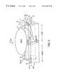
- FIG. 2illustrates a perspective view of a first preferred embodiment of the present invention
- FIG. 3illustrates a cross sectional view of a first preferred embodiment of the present invention
- FIG. 4illustrates a perspective view of a second preferred embodiment of the present invention
- FIG. 5illustrates a cross sectional side view of a second preferred embodiment of the present invention
- FIG. 6illustrates a perspective view of a first novel anode assembly in accordance with the preferred embodiment of the present invention
- FIG. 7illustrates a cross sectional view of a first novel anode assembly in accordance with the preferred embodiment of the present invention
- FIG. 8illustrates a perspective view of a second novel anode assembly in accordance with the preferred embodiment of the present invention
- FIG. 9illustrates a cross sectional view of a second novel anode assembly in accordance with the preferred embodiment of the present invention.
- FIG. 10illustrates a cross sectional view of a “proximity plating” apparatus and method in accordance with the preferred embodiment of the present invention
- FIG. 11illustrates a cross sectional view of a substrate having various layers and grains disposed thereon.
- FIGS. 12A-12Billustrate cross sectional views of a method for advantageously affecting the texture of a conductive material in accordance with the preferred embodiment of the present invention.
- FIGS. 1-12The preferred embodiments of the present invention will now be described with reference to FIGS. 1-12.
- conventional processinguses different equipment, at different times, to obtain conductive material within holes and trenches, or at other desired locations on the surface of a semiconductor wafer that contains many different semiconductor chips. Accordingly, the equipment cost needed to manufacture a high quality semiconductor integrated circuit device can be exorbitant.
- the present inventioncontemplates different embodiments, which allow for the same apparatus, to be used to plate/deposit a conductive material onto the surface and into the contact, via holes, and trenches, as well as to polish the wafer surface. While the present invention can be used with any conductive material, it is especially suited for use with copper as the conductor, and for use in the fabrication of ULSI integrated circuits having submicron features with large aspect ratios. Furthermore, although a semiconductor wafer will be used to describe the preferred embodiments of the present invention, other semiconductor workpieces such as a flat panel or magnetic film head may be used in accordance with the present invention.
- FIG. 1illustrates a section of a wafer 2 where a via is to be formed.
- the viaas known in the semiconductor arts, is a conductive material that electrically couples different circuit layers.
- the viacontains a conductor 8 that can connect a lower level conductive layer 4 with an upper level conductive layer 6 , with an insulative material 10 disposed therearound. It is understood that the present invention can operate upon any metal layer of a multi-layer integrated circuit chip.
- FIG. 2illustrates a perspective view
- FIG. 3illustrates a cross sectional view of a first preferred embodiment of the present invention.
- a conductive materialpreferably copper
- the first chamber 100is separated from the second chamber 200 by a center partition 60 .
- the first and second chambers 100 , 200each include an anode assembly 12 , 14 having a circular or square mechanical pad 16 , 18 mounted on a cylindrical anode 20 , 22 that rotates around a first axis 24 , and a wafer head assembly 26 having a wafer 2 that rotates around a second axis 28 .
- the entire wafer head assembly 26is further adapted to move side to side in the direction of arrow 30 so that the center area of the wafer 2 can be plated and polished.
- the cylindrical anodes 20 , 22are connected to shafts 32 , 34 for rotating about axis 24 .
- the wafer 2rotates within an area that is covered by the mechanical pads 16 , 18 , as will be described in further detail hereinafter, which area is within chambers 100 , 200 that keeps the electrolyte solution 11 disposed therein.
- the wafer head assemblies 26could be used with the present invention.
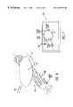
- the wafer head assembly 26may include a nonconductive, preferably circular, chuck 36 with a cavity that is preferably a few millimeters deep at its center and which cavity may contain a resting pad (not shown).
- the wafer 2is loaded into the cavity, backside first, against the resting pad using a conventional type of transport or vacuum mechanism to ensure that the wafer 2 is stationary with respect to the wafer head assembly 26 while in use.
- a nonconductive retaining ring 40such as an O-ring or other rubber type of seal at the periphery of the wafer head assembly 26 and a cathode contact electrode 38 each push against the edge of the wafer 2 and hold the wafer 2 in place.
- the entire back side of the wafer 2 which pushes against the chuck 36 that is under the retaining ring 40is thus protected from any and all solutions, including electrolyte.
- Other conventional wafer head assembliescan be used in accordance with the present invention.
- the electric potentialcan be applied to the wafer using a ring conductor.
- other methods of applying the electric potential to the wafermay be used in accordance with the present invention.
- a liquid conductor or an inflatable tube coated with a conductive materialmay be used in the present invention.
- An example of using the liquid conductor or the conductive tube to provide the necessary electric potential according to the present inventionis disclosed in the co-pending U.S. application Ser. No. 09/283,024, filed Mar. 30, 1999, entitled “Method And Apparatus For Forming an Electric Contact With a Semiconductor Substrate”, commonly owned by the assignee of the present invention, the contents of which are expressly incorporated herein by reference.
- the first chamber 100may be used for plating and the second chamber 200 may be used for polishing.
- the two chambers 100 , 200can be used interchangeably where the first chamber 100 can be used for polishing and the second chamber 200 can be used for plating.
- the first chamber 100includes the first anode assembly 12 for plating and the second chamber 200 includes the second anode assembly 14 for electropolishing.
- Electric potentialsare applied to the anode 20 , the anode 22 and the wafer 2 .
- Any known method for providing the electric potentials to the two cylindrical anodescan be used in the present invention.
- the difference in the amount of electric potential applied to each of the two cylindrical anodes 20 , 22determines which anode assembly is used for plating and which one is used for electropolishing.
- An electrolyte solution 11is flowed from bottom openings 50 of the two chambers 100 , 200 until the solution 11 makes contact with the pads 16 , 18 .
- the electrolyte solution 11is further circulated via side openings 52 to channel 54 to the bottom openings 50 .
- the electrolyte solution 11can be originally fed into the first and second chambers 100 , 200 via a reservoir (not shown) through an in-channel (not shown).
- a first electric potential difference between the cylindrical anode 20 and the cathode wafer 2allows the metal in the electrolyte solution 11 to be plated on the wafer surface via pad 16 .
- polishing of the waferis undertaken by a second electrical potential difference between the cylindrical anode 22 and the cathode wafer 2 .
- the plating process of the present inventioncan be implemented using a brush plating method or an “electro chemical mechanical deposition” method.
- a brush plating methodor an “electro chemical mechanical deposition” method.
- electrochemical mechanical depositionA more detailed description of the “electro chemical mechanical deposition” method can be found in the co-pending U.S. application Ser. No. 09/201,929, now U.S. Pat. No. 6,176,992 and titled “Method and Apparatus For Electro Chemical Mechanical Deposition”, commonly owned by the assignee of the present invention, the contents of which are expressly incorporated herein by reference.
- the polishing process of the present inventionmay be implemented by way of electropolishing or by chemical mechanical polishing as described in more detail hereinafter.
- the roller-shaped mechanical pad 18polishes the wafer similar to the manner in which a roller sander removes paints from a wall.
- the mechanical pad 18can have a size that polishes a section of the wafer 2 at any given time.
- One or more drive assembliesare also included to rotate the cylindrical anodes 20 , 22 , and thereby the mechanical pads 16 , 18 , so that they are in contact with the section of the wafer 2 that needs to be plated and polished.
- the mechanical pads 16 , 18are preferably made of a nonconductive, porous type material such as polyurethane.
- the mechanical pads 16 , 18preferably have a circular shape, but may be shaped in any other form so long as they can effectively plate and/or polish the wafer.
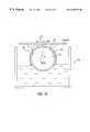
- FIG. 4illustrates a perspective view
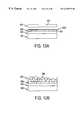
- FIG. 5illustrates a cross sectional view of a second preferred embodiment of the present invention.
- the second preferred embodimentis also implemented with a first chamber 300 for plating and a second chamber 400 for polishing the wafer 2 .
- the first chamber 300is separated from the second chamber 400 by a center partition/wall 460 .
- the first chamber 300includes an anode plate 306 on the bottom of the chamber 300 . Any known method for attaching the anode plate 306 or shape to the bottom of the chamber 300 may be used.
- the electrolyte solution 11is circulated via drain channels 302 to the bottom opening 304 , or through the anode plate 306 .
- the second chamber 400includes a mechanical pad 402 mounted on a cylindrical roller 404 for chemical mechanical polishing (CMP) of the wafer 2 .
- a shaft 406is used to rotate the roller around axis 408 .
- CMPis a material planarization process that combines chemical removal of semiconductor layers such as insulators or metals with mechanical buffering of the substrate surface.
- CMPmay provide global planarization of the wafer surface. For example, during the wafer fabrication process, CMP is often used to polish the profiles that build up in multilevel metal interconnection schemes.
- the apparatusapplies, using a power source, a negative potential to the cathode contact 38 and a positive potential to the anode plate/shade 306 .
- a negative potentialto the cathode contact 38
- a positive potentialto the anode plate/shade 306 .
- the mechanical pad assembly 412substantially prevents metals from becoming permanently deposited on surfaces of the wafer 2 where such a deposit is undesired, due to the polishing or rubbing action of the mechanical pad 402 . Accordingly, metal, i.e. copper, is deposited in vias, trenches, and the like where desired, and is substantially prevented from being deposited in undesired areas such as the surface or field area on the wafer.
- the wafer head assembly 26faces toward the mechanical pad assembly 412 , and is pushed down with a controlled force.
- the wafer head assembly 26is similar to that described with reference to FIGS. 2 and 3 and rotates around axis 28 using a conventional motorized spindle (not shown).
- the wafer head assembly 26is also adapted to move side to side in the direction of arrow 30 so that the center area of the wafer 2 may be plated and polished.
- the present inventionmay reduce the need for pulse generating power supplies because the mechanical pulsing that is generated from the movement of the pad creates sufficient pulsing. This mechanical pulsing is created as a result of the wafer being in contact with the pad as it is moved in relation to the wafer. The benefit of the mechanical pulsing is that it improves grain size and copper film integrity without the need for power supplies with pulsing capabilities.
- the scope of the present inventioncontemplates interchanging the plating methods and the polishing methods of the first and second preferred embodiments of the invention with each other.
- the CMP method of the second preferred embodimentcan be interchanged with the electropolishing method of the first preferred embodiment.
- the plating method of the first embodimentcan be interchanged with the plating method of the second embodiment.
- the present inventioncan be implemented with any number of containers using various plating and polishing methods to achieve the objects of the present invention.
- three chambersmay be used in the present invention where the center chamber can be used for polishing while the left and right chambers can be used for plating/depositing.
- the present invention as illustrated in FIGS. 6-9further describes a method and apparatus for intermittently applying the conductive material to the semiconductor substrate and also intermittently polishing the substrate when such conductive material is not being applied to the substrate.
- the present inventionapplies electrical current having a potential difference between the workpiece and the anode so that the conductive material can be applied to the workpiece when such current is applied. Further, reverse current pulses can be applied between the workpiece.
- FIG. 6illustrates a perspective view
- FIG. 7illustrates a cross sectional view of a first anode assembly in accordance with the present invention.
- the anode assembly 500includes a unique anode-pad arrangement for both plating and polishing the workpiece 802 . Multiple strips of pad 502 are attached, glued, or machined onto a cylindrical anode 504 such that the pad 502 protrudes from the outer surface of the anode 504 . Electric power is applied to the cylindrical anode 504 and the cathode workpiece 802 .
- the workpiece 802is plated when the anode 504 is facing the workpiece (cathode) 802 with no pad in between, and it is polished when the pad 502 is in mechanical contact with the workpiece 802 .
- the workpiece 802is further adapted to move side to side via workpiece head assembly (not shown), if needed, as indicated by arrow 520 .
- Such unique plating and polishingresults from the anode assembly 500 because of the mechanical polishing effects caused by the brushing of the pad 502 against the workpiece surface, and plating of metal from the anode, electrolyte, and workpiece configuration.
- FIG. 8illustrates a perspective view
- FIG. 9illustrates a cross sectional view of a second anode assembly in accordance with the present invention.
- the anode assembly 600also includes a unique anode-pad arrangement for both plating and polishing the workpiece 802 .
- the anode assembly 600is formed in a donut or circular shape having a hole 606 in the center. Multiple strips of pad 602 are mounted on the anode 604 such that the pad 602 protrudes from the surface of the anode 604 .
- the workpiece 802When electric power is applied to the anode 604 and the cathode workpiece 802 , and as the anode 604 rotates about a first axis 610 and the workpiece 802 rotates about a second axis 612 , the workpiece 802 is plated when the anode 604 is facing the workpiece 802 with no pad in between, and it is polished when the pad 602 is in mechanical contact with the workpiece 802 . As described above, such unique plating and polishing results from the anode assembly 600 because of the mechanical polishing effects caused by the brushing of the pad 602 against the workpiece surface.
- the diameter or size of the anode assembly 600may also be smaller than the diameter or size of the workpiece 802 .
- the electrolyte or other solutioncan be introduced to the mechanical pads 502 , 602 from a reservoir (not shown) located in proximity to the anodes 504 , 604 .
- the anodes 504 , 604can have an in-channel that includes passageways within the center of anodes 504 , 604 and holes that are made in the anode 504 , 604 , which together provide a path for the solution to be fed to the gap between the anode and the cathode.
- the electrolyte solutioncan be dispensed directly onto the anode assemblies 500 , 600 through another channel in accordance with the methods described earlier herein.
- the electrolyte solutionmay be contained within a non-conductive chamber 530 that is created around the workpiece. O-rings and other conventional structures, as described earlier herein, may be used to contain the solution within the chamber 530 in this embodiment.
- the need for leveling agentsmay be reduced, or needed in a smaller percentage than conventionally used.
- novel anode assemblies illustrated in FIGS. 6-9can be used to primarily plate/deposit the conductive material on the workpiece surface without polishing the same surface. This is accomplished when the pad or other fixed feature is used only in proximity of the workpiece surface to improve electrolyte mass transfer.
- FIG. 10illustrates a cross sectional view of a “proximity plating” apparatus and method in accordance with the present invention.
- FIG. 10illustrates a nonconductive chamber 700 having the electrolyte solution 11 disposed therein.
- the chamber 700includes the anode assembly 500 having multiple strips of pad 502 or fixed features mounted, or machined onto the cylindrical anode 504 .
- the pad strips 502are rotating about axis 510 and are spaced apart from the workpiece 802 (the pad strips 502 do not make direct contact with the workpiece 802 ), the workpiece 802 is plated using the electrolyte solution 11 .
- the anode 510 and pad strips 502should preferably rotate at a rate such that the electrolyte solution 11 is continuous and is applied/splashed to the workpiece 802 , and thus forming a closed electrical circuit through the anode assembly 500 , electrolyte, and the workpiece (cathode) 802 .
- a gap 800is about 0-5 mm and contains a meniscus solution of electrolyte, a very high mass transport results, thereby depositing high quality metal films onto the workpiece surface.
- the gap 800may be greater than 5 mm.
- the hardness of the pad or fixtureis coupled with the relative speed of travel of the pad to the workpiece.
- the padshould be porous and hard for optimal performance.
- the present inventionmay reduce the need for pulse generating power supplies because the mechanical pulsing that is generated from the movement of the pad relative to the face of the workpiece creates sufficient pulsing. This mechanical pulsing is created as a result of the wafer being in proximity with the pad as it is moved in relation to the workpiece.
- the benefit of the mechanical pulsingis that it improves grain size, filling efficiency of the contact holes, vias, and trenches, and copper film integrity without the need for power supplies with pulsing capabilities.
- FIGS. 11 and 12 A- 12 Bwill now be used to describe an improved embodiment of the present invention. It has been determined that the present invention can also advantageously affect the texture of a conductive material that has been applied using a plating process.
- FIG. 11illustrates a conventional substrate 900 , having deposited thereon a barrier layer 902 and an epitaxial seed layer 904 .
- the seed layer 904is composed of individual grains 906 , which are oriented in a predetermined manner, such as a ⁇ 111> crystal orientation.
- the atoms that make up the conductive plating layer 908 applied theretowill, over time, cluster to form grains 910 , which grains 910 retain the original crystal orientation of the seed layer 904 disposed below. Accordingly, if the seed layer 904 has a ⁇ 111> crystal orientation, so will the conductive plating layer 908 .
- the present inventionhas found that by plating and polishing, as described above, the polishing changes the crystal orientation of the applied conductive plating layer to become more random.
- the polishersuch as pad 402 previously described, polishes the first level of atoms and causes dangling bonds in the atoms at that first level.
- the next level of atoms applied thereoverwill not form in the same manner as the first level was formed.
Landscapes
- Chemical & Material Sciences (AREA)
- Engineering & Computer Science (AREA)
- Chemical Kinetics & Catalysis (AREA)
- Electrochemistry (AREA)
- Materials Engineering (AREA)
- Metallurgy (AREA)
- Organic Chemistry (AREA)
- Crystallography & Structural Chemistry (AREA)
- Mechanical Engineering (AREA)
- Life Sciences & Earth Sciences (AREA)
- Sustainable Development (AREA)
- Manufacturing & Machinery (AREA)
- Condensed Matter Physics & Semiconductors (AREA)
- General Physics & Mathematics (AREA)
- Physics & Mathematics (AREA)
- Computer Hardware Design (AREA)
- Microelectronics & Electronic Packaging (AREA)
- Power Engineering (AREA)
- Electroplating Methods And Accessories (AREA)
- Internal Circuitry In Semiconductor Integrated Circuit Devices (AREA)
- Electrodes Of Semiconductors (AREA)
- Mechanical Treatment Of Semiconductor (AREA)
Abstract
Description
Claims (50)
Priority Applications (16)
| Application Number | Priority Date | Filing Date | Title |
|---|---|---|---|
| US09/285,621US6328872B1 (en) | 1999-04-03 | 1999-04-03 | Method and apparatus for plating and polishing a semiconductor substrate |
| US09/373,681US6409904B1 (en) | 1998-12-01 | 1999-08-13 | Method and apparatus for depositing and controlling the texture of a thin film |
| DE60015513TDE60015513T2 (en) | 1999-04-03 | 2000-03-29 | METHOD AND DEVICE FOR PLATING AND POLISHING A SEMICONDUCTOR COMPONENT |
| KR1020017012505AKR100778131B1 (en) | 1999-04-03 | 2000-03-29 | Plating and Polishing Device for Semiconductor Substrates |
| JP2000609226AJP2002541655A (en) | 1999-04-03 | 2000-03-29 | Method and apparatus for plating and polishing |
| EP00918491AEP1169162B1 (en) | 1999-04-03 | 2000-03-29 | Method and apparatus for plating and polishing a semiconductor substrate |
| AU39292/00AAU3929200A (en) | 1999-04-03 | 2000-03-29 | Method and apparatus for plating and polishing a semiconductor substrate |
| CNB008079641ACN1268470C (en) | 1999-04-03 | 2000-03-29 | Method and apparatus for plating and polishing a semiconductor substrate |
| AT00918491TATE281277T1 (en) | 1999-04-03 | 2000-03-29 | METHOD AND DEVICE FOR PLATING AND POLISHING A SEMICONDUCTOR COMPONENT |
| PCT/US2000/008336WO2000059682A1 (en) | 1999-04-03 | 2000-03-29 | Method and apparatus for plating and polishing a semiconductor substrate |
| TW089106166ATW506022B (en) | 1999-04-03 | 2000-04-01 | Apparatus and method for plating and polishing a surface of a semiconductor workpiece, a pad assembly for plating and polishing a semiconductor workpiece, an anode assembly for plating a semiconductor workpiece |
| US09/941,360US6797132B2 (en) | 1999-04-03 | 2001-08-28 | Apparatus for plating and polishing a semiconductor workpiece |
| US10/165,673US6837979B2 (en) | 1998-12-01 | 2002-06-06 | Method and apparatus for depositing and controlling the texture of a thin film |
| US10/302,755US7204917B2 (en) | 1998-12-01 | 2002-11-21 | Workpiece surface influencing device designs for electrochemical mechanical processing and method of using the same |
| US10/946,703US7309406B2 (en) | 1999-04-03 | 2004-09-21 | Method and apparatus for plating and polishing semiconductor substrate |
| US11/786,948US7670473B1 (en) | 1998-12-01 | 2007-04-12 | Workpiece surface influencing device designs for electrochemical mechanical processing and method of using the same |
Applications Claiming Priority (1)
| Application Number | Priority Date | Filing Date | Title |
|---|---|---|---|
| US09/285,621US6328872B1 (en) | 1999-04-03 | 1999-04-03 | Method and apparatus for plating and polishing a semiconductor substrate |
Related Parent Applications (1)
| Application Number | Title | Priority Date | Filing Date |
|---|---|---|---|
| US09/201,929Continuation-In-PartUS6176992B1 (en) | 1998-11-03 | 1998-12-01 | Method and apparatus for electro-chemical mechanical deposition |
Related Child Applications (4)
| Application Number | Title | Priority Date | Filing Date |
|---|---|---|---|
| US09/201,929Continuation-In-PartUS6176992B1 (en) | 1998-11-03 | 1998-12-01 | Method and apparatus for electro-chemical mechanical deposition |
| US09/373,681Continuation-In-PartUS6409904B1 (en) | 1998-12-01 | 1999-08-13 | Method and apparatus for depositing and controlling the texture of a thin film |
| US09/941,360DivisionUS6797132B2 (en) | 1999-04-03 | 2001-08-28 | Apparatus for plating and polishing a semiconductor workpiece |
| US10/302,755Continuation-In-PartUS7204917B2 (en) | 1998-12-01 | 2002-11-21 | Workpiece surface influencing device designs for electrochemical mechanical processing and method of using the same |
Publications (1)
| Publication Number | Publication Date |
|---|---|
| US6328872B1true US6328872B1 (en) | 2001-12-11 |
Family
ID=23095034
Family Applications (3)
| Application Number | Title | Priority Date | Filing Date |
|---|---|---|---|
| US09/285,621Expired - LifetimeUS6328872B1 (en) | 1998-12-01 | 1999-04-03 | Method and apparatus for plating and polishing a semiconductor substrate |
| US09/941,360Expired - Fee RelatedUS6797132B2 (en) | 1999-04-03 | 2001-08-28 | Apparatus for plating and polishing a semiconductor workpiece |
| US10/946,703Expired - LifetimeUS7309406B2 (en) | 1999-04-03 | 2004-09-21 | Method and apparatus for plating and polishing semiconductor substrate |
Family Applications After (2)
| Application Number | Title | Priority Date | Filing Date |
|---|---|---|---|
| US09/941,360Expired - Fee RelatedUS6797132B2 (en) | 1999-04-03 | 2001-08-28 | Apparatus for plating and polishing a semiconductor workpiece |
| US10/946,703Expired - LifetimeUS7309406B2 (en) | 1999-04-03 | 2004-09-21 | Method and apparatus for plating and polishing semiconductor substrate |
Country Status (10)
| Country | Link |
|---|---|
| US (3) | US6328872B1 (en) |
| EP (1) | EP1169162B1 (en) |
| JP (1) | JP2002541655A (en) |
| KR (1) | KR100778131B1 (en) |
| CN (1) | CN1268470C (en) |
| AT (1) | ATE281277T1 (en) |
| AU (1) | AU3929200A (en) |
| DE (1) | DE60015513T2 (en) |
| TW (1) | TW506022B (en) |
| WO (1) | WO2000059682A1 (en) |
Cited By (97)
| Publication number | Priority date | Publication date | Assignee | Title |
|---|---|---|---|---|
| US20020144894A1 (en)* | 2000-01-03 | 2002-10-10 | Daniel Woodruff | Processing apparatus including a reactor for electrochemically etching a microelectronic workpiece |
| US6464855B1 (en)* | 2000-10-04 | 2002-10-15 | Speedfam-Ipec Corporation | Method and apparatus for electrochemical planarization of a workpiece |
| US20030057097A1 (en)* | 2001-09-21 | 2003-03-27 | Applied Materials, Inc. | Method and apparatus for forming metal layers |
| US6572755B2 (en) | 2001-04-11 | 2003-06-03 | Speedfam-Ipec Corporation | Method and apparatus for electrochemically depositing a material onto a workpiece surface |
| US20030113509A1 (en)* | 2001-12-13 | 2003-06-19 | 3M Innovative Properties Company | Abrasive article for the deposition and polishing of a conductive material |
| US20030121774A1 (en)* | 1998-12-01 | 2003-07-03 | Uzoh Cyprian E. | Workpiece surface influencing device designs for electrochemical mechanical processing and method of using the same |
| US20030136684A1 (en)* | 2002-01-22 | 2003-07-24 | Applied Materials, Inc. | Endpoint detection for electro chemical mechanical polishing and electropolishing processes |
| US20030146102A1 (en)* | 2002-02-05 | 2003-08-07 | Applied Materials, Inc. | Method for forming copper interconnects |
| US6612915B1 (en)* | 1999-12-27 | 2003-09-02 | Nutool Inc. | Work piece carrier head for plating and polishing |
| US20030181139A1 (en)* | 2002-02-04 | 2003-09-25 | Kurt Lehman | Windows configurable to be coupled to a process tool or to be disposed within an opening in a polishing pad |
| US20030226757A1 (en)* | 2002-06-07 | 2003-12-11 | Smith Taber H. | Dummy fill for integrated circuits |
| US20030229410A1 (en)* | 2002-06-07 | 2003-12-11 | Smith Taber H. | Integrated circuit metrology |
| US20030229875A1 (en)* | 2002-06-07 | 2003-12-11 | Smith Taber H. | Use of models in integrated circuit fabrication |
| US20030229479A1 (en)* | 2002-06-07 | 2003-12-11 | Smith Taber H. | Dummy fill for integrated circuits |
| US20030228714A1 (en)* | 2002-06-07 | 2003-12-11 | Smith Taber H. | Dummy fill for integrated circuits |
| US20030234182A1 (en)* | 2002-06-19 | 2003-12-25 | Tatyana Andryushchenko | Method of fabricating damascene structures in mechanically weak interlayer dielectrics |
| US20040050817A1 (en)* | 1999-11-29 | 2004-03-18 | Lizhong Sun | Advanced electrolytic polish (AEP) assisted metal wafer planarization method and apparatus |
| US20040055873A1 (en)* | 2002-09-24 | 2004-03-25 | Digital Matrix Corporation | Apparatus and method for improved electroforming |
| US20040094403A1 (en)* | 2002-11-14 | 2004-05-20 | International Business Machines Corporation | Integrated plating and planarization apparatus having a variable-diameter counterelectrode |
| US20040094427A1 (en)* | 2002-11-14 | 2004-05-20 | International Business Machines Corporation | Integrated plating and planarization process and apparatus therefor |
| US20040134793A1 (en)* | 2000-01-14 | 2004-07-15 | Uzoh Cyprian Emeka | Workpiece proximity etching method and apparatus |
| US20040140203A1 (en)* | 2003-01-21 | 2004-07-22 | Applied Materials,Inc. | Liquid isolation of contact rings |
| US20040149573A1 (en)* | 2003-01-31 | 2004-08-05 | Applied Materials, Inc. | Contact ring with embedded flexible contacts |
| US20040182424A1 (en)* | 2003-03-17 | 2004-09-23 | Novellus Systems, Inc. | Active rinse shield for electrofill chemical bath and method of use |
| US6796887B2 (en) | 2002-11-13 | 2004-09-28 | Speedfam-Ipec Corporation | Wear ring assembly |
| US6802955B2 (en) | 2002-01-11 | 2004-10-12 | Speedfam-Ipec Corporation | Method and apparatus for the electrochemical deposition and planarization of a material on a workpiece surface |
| US20040200732A1 (en)* | 2003-04-14 | 2004-10-14 | Basol Bulent M. | Method and apparatus for eliminating defects and improving uniformity in electrochemically processed conductive layers |
| US20040211662A1 (en)* | 2003-04-22 | 2004-10-28 | Saket Chadda | Method and apparatus for the electrochemical deposition and removal of a material on a workpiece surface |
| US20040245094A1 (en)* | 2003-06-06 | 2004-12-09 | Mchugh Paul R. | Integrated microfeature workpiece processing tools with registration systems for paddle reactors |
| US6835657B2 (en) | 2002-12-02 | 2004-12-28 | Applied Materials, Inc. | Method for recrystallizing metal in features of a semiconductor chip |
| US20050000817A1 (en)* | 2003-07-01 | 2005-01-06 | Mchugh Paul R. | Reactors having multiple electrodes and/or enclosed reciprocating paddles, and associated methods |
| US6843904B1 (en)* | 1999-10-21 | 2005-01-18 | Matsushita Electric Industrial Co., Ltd. | Inspection and repair of active type substrate |
| US20050016861A1 (en)* | 2003-07-24 | 2005-01-27 | Thomas Laursen | Method for planarizing a work piece |
| US6855239B1 (en) | 2002-09-27 | 2005-02-15 | Rahul Jairath | Plating method and apparatus using contactless electrode |
| US20050034977A1 (en)* | 2003-06-06 | 2005-02-17 | Hanson Kyle M. | Electrochemical deposition chambers for depositing materials onto microfeature workpieces |
| US20050050767A1 (en)* | 2003-06-06 | 2005-03-10 | Hanson Kyle M. | Wet chemical processing chambers for processing microfeature workpieces |
| US20050132306A1 (en)* | 2002-06-07 | 2005-06-16 | Praesagus, Inc., A Massachusetts Corporation | Characterization and reduction of variation for integrated circuits |
| US20050218000A1 (en)* | 2004-04-06 | 2005-10-06 | Applied Materials, Inc. | Conditioning of contact leads for metal plating systems |
| US6962524B2 (en) | 2000-02-17 | 2005-11-08 | Applied Materials, Inc. | Conductive polishing article for electrochemical mechanical polishing |
| US20050282371A1 (en)* | 2001-04-05 | 2005-12-22 | Novellus Systems, Inc. | Sequential station tool for wet processing of semiconductor wafers |
| US6979248B2 (en) | 2002-05-07 | 2005-12-27 | Applied Materials, Inc. | Conductive polishing article for electrochemical mechanical polishing |
| US6988942B2 (en) | 2000-02-17 | 2006-01-24 | Applied Materials Inc. | Conductive polishing article for electrochemical mechanical polishing |
| US6991526B2 (en) | 2002-09-16 | 2006-01-31 | Applied Materials, Inc. | Control of removal profile in electrochemically assisted CMP |
| US6991528B2 (en) | 2000-02-17 | 2006-01-31 | Applied Materials, Inc. | Conductive polishing article for electrochemical mechanical polishing |
| US7014538B2 (en) | 1999-05-03 | 2006-03-21 | Applied Materials, Inc. | Article for polishing semiconductor substrates |
| US7025861B2 (en) | 2003-02-06 | 2006-04-11 | Applied Materials | Contact plating apparatus |
| US7029365B2 (en) | 2000-02-17 | 2006-04-18 | Applied Materials Inc. | Pad assembly for electrochemical mechanical processing |
| US7059948B2 (en) | 2000-12-22 | 2006-06-13 | Applied Materials | Articles for polishing semiconductor substrates |
| US7070475B2 (en) | 2002-09-16 | 2006-07-04 | Applied Materials | Process control in electrochemically assisted planarization |
| US7077721B2 (en) | 2000-02-17 | 2006-07-18 | Applied Materials, Inc. | Pad assembly for electrochemical mechanical processing |
| US7084064B2 (en) | 2004-09-14 | 2006-08-01 | Applied Materials, Inc. | Full sequence metal and barrier layer electrochemical mechanical processing |
| US20060175191A1 (en)* | 2003-03-19 | 2006-08-10 | Osamu Nabeya | Composite machining device and method |
| US7112270B2 (en) | 2002-09-16 | 2006-09-26 | Applied Materials, Inc. | Algorithm for real-time process control of electro-polishing |
| US7125477B2 (en) | 2000-02-17 | 2006-10-24 | Applied Materials, Inc. | Contacts for electrochemical processing |
| US7137879B2 (en) | 2001-04-24 | 2006-11-21 | Applied Materials, Inc. | Conductive polishing article for electrochemical mechanical polishing |
| US7186164B2 (en) | 2003-12-03 | 2007-03-06 | Applied Materials, Inc. | Processing pad assembly with zone control |
| US20070144912A1 (en)* | 2003-07-01 | 2007-06-28 | Woodruff Daniel J | Linearly translating agitators for processing microfeature workpieces, and associated methods |
| US20070153453A1 (en)* | 2006-01-05 | 2007-07-05 | Applied Materials, Inc. | Fully conductive pad for electrochemical mechanical processing |
| US20070157139A1 (en)* | 2002-06-07 | 2007-07-05 | David White | Characterization and verification for integrated circuit designs |
| US20070235344A1 (en)* | 2006-04-06 | 2007-10-11 | Applied Materials, Inc. | Process for high copper removal rate with good planarization and surface finish |
| US7285195B2 (en) | 2004-06-24 | 2007-10-23 | Applied Materials, Inc. | Electric field reducing thrust plate |
| US20070251832A1 (en)* | 2006-04-27 | 2007-11-01 | Applied Materials, Inc. | Method and apparatus for electrochemical mechanical polishing of cu with higher liner velocity for better surface finish and higher removal rate during clearance |
| US20070256039A1 (en)* | 2002-06-07 | 2007-11-01 | Cadence Design Systems, Inc. | Dummy fill for integrated circuits |
| US7303462B2 (en) | 2000-02-17 | 2007-12-04 | Applied Materials, Inc. | Edge bead removal by an electro polishing process |
| US7303662B2 (en) | 2000-02-17 | 2007-12-04 | Applied Materials, Inc. | Contacts for electrochemical processing |
| US7323095B2 (en) | 2000-12-18 | 2008-01-29 | Applied Materials, Inc. | Integrated multi-step gap fill and all feature planarization for conductive materials |
| US20080027698A1 (en)* | 2002-06-07 | 2008-01-31 | Cadence Design Systems, Inc. | Method and System for Handling Process Related Variations for Integrated Circuits Based Upon Reflections |
| US7344432B2 (en) | 2001-04-24 | 2008-03-18 | Applied Materials, Inc. | Conductive pad with ion exchange membrane for electrochemical mechanical polishing |
| US7374644B2 (en) | 2000-02-17 | 2008-05-20 | Applied Materials, Inc. | Conductive polishing article for electrochemical mechanical polishing |
| US7390744B2 (en) | 2004-01-29 | 2008-06-24 | Applied Materials, Inc. | Method and composition for polishing a substrate |
| US20080181758A1 (en)* | 2007-01-29 | 2008-07-31 | Woodruff Daniel J | Microfeature workpiece transfer devices with rotational orientation sensors, and associated systems and methods |
| US20080178460A1 (en)* | 2007-01-29 | 2008-07-31 | Woodruff Daniel J | Protected magnets and magnet shielding for processing microfeature workpieces, and associated systems and methods |
| US7422982B2 (en) | 2006-07-07 | 2008-09-09 | Applied Materials, Inc. | Method and apparatus for electroprocessing a substrate with edge profile control |
| US7427340B2 (en) | 2005-04-08 | 2008-09-23 | Applied Materials, Inc. | Conductive pad |
| US20080242202A1 (en)* | 2007-04-02 | 2008-10-02 | Yuchun Wang | Extended pad life for ecmp and barrier removal |
| US7449098B1 (en) | 1999-10-05 | 2008-11-11 | Novellus Systems, Inc. | Method for planar electroplating |
| US7520968B2 (en) | 2004-10-05 | 2009-04-21 | Applied Materials, Inc. | Conductive pad design modification for better wafer-pad contact |
| US7531079B1 (en) | 1998-10-26 | 2009-05-12 | Novellus Systems, Inc. | Method and apparatus for uniform electropolishing of damascene IC structures by selective agitation |
| US20090245984A1 (en)* | 2008-03-27 | 2009-10-01 | Lam Research Corporation | High throughput cleaner chamber |
| US20090277802A1 (en)* | 1998-10-26 | 2009-11-12 | Novellus Systems, Inc. | Pad-assisted electropolishing |
| US20090277867A1 (en)* | 2003-10-20 | 2009-11-12 | Novellus Systems, Inc. | Topography reduction and control by selective accelerator removal |
| US7655565B2 (en) | 2005-01-26 | 2010-02-02 | Applied Materials, Inc. | Electroprocessing profile control |
| US7670468B2 (en) | 2000-02-17 | 2010-03-02 | Applied Materials, Inc. | Contact assembly and method for electrochemical mechanical processing |
| US7678245B2 (en) | 2000-02-17 | 2010-03-16 | Applied Materials, Inc. | Method and apparatus for electrochemical mechanical processing |
| US7790015B2 (en) | 2002-09-16 | 2010-09-07 | Applied Materials, Inc. | Endpoint for electroprocessing |
| US7799200B1 (en) | 2002-07-29 | 2010-09-21 | Novellus Systems, Inc. | Selective electrochemical accelerator removal |
| US20110236159A1 (en)* | 2010-03-24 | 2011-09-29 | Lam Research Corporation | Reduction of particle contamination produced by moving mechanisms in a process tool |
| US8168540B1 (en) | 2009-12-29 | 2012-05-01 | Novellus Systems, Inc. | Methods and apparatus for depositing copper on tungsten |
| US20130084400A1 (en)* | 2011-09-29 | 2013-04-04 | Masako Kodera | Substrate processing method |
| US8530359B2 (en) | 2003-10-20 | 2013-09-10 | Novellus Systems, Inc. | Modulated metal removal using localized wet etching |
| US8562272B2 (en) | 2010-02-16 | 2013-10-22 | Lam Research Corporation | Substrate load and unload mechanisms for high throughput |
| US20140042030A1 (en)* | 2012-08-10 | 2014-02-13 | General Electric Company | Sealed laminated structure, system and method for electrolytic processing the same |
| US8893642B2 (en) | 2010-03-24 | 2014-11-25 | Lam Research Corporation | Airflow management for low particulate count in a process tool |
| US9393759B2 (en) | 2013-10-24 | 2016-07-19 | General Electric Company | Metal laminate structures with systems and methods for treating |
| US10876198B2 (en) | 2015-02-10 | 2020-12-29 | Arcanum Alloys, Inc. | Methods and systems for slurry coating |
| US11261516B2 (en) | 2016-05-20 | 2022-03-01 | Public Joint Stock Company “Severstal” | Methods and systems for coating a steel substrate |
| US20220220628A1 (en)* | 2021-01-13 | 2022-07-14 | Corrdesa, LLC | Electrochemical treatment system |
Families Citing this family (56)
| Publication number | Priority date | Publication date | Assignee | Title |
|---|---|---|---|---|
| US6719615B1 (en) | 2000-10-10 | 2004-04-13 | Beaver Creek Concepts Inc | Versatile wafer refining |
| US6341998B1 (en)* | 1999-11-04 | 2002-01-29 | Vlsi Technology, Inc. | Integrated circuit (IC) plating deposition system and method |
| US6379223B1 (en) | 1999-11-29 | 2002-04-30 | Applied Materials, Inc. | Method and apparatus for electrochemical-mechanical planarization |
| US20040020789A1 (en)* | 2000-02-17 | 2004-02-05 | Applied Materials, Inc. | Conductive polishing article for electrochemical mechanical polishing |
| US20080156657A1 (en)* | 2000-02-17 | 2008-07-03 | Butterfield Paul D | Conductive polishing article for electrochemical mechanical polishing |
| US20050092621A1 (en)* | 2000-02-17 | 2005-05-05 | Yongqi Hu | Composite pad assembly for electrochemical mechanical processing (ECMP) |
| US20040182721A1 (en)* | 2003-03-18 | 2004-09-23 | Applied Materials, Inc. | Process control in electro-chemical mechanical polishing |
| US6537144B1 (en) | 2000-02-17 | 2003-03-25 | Applied Materials, Inc. | Method and apparatus for enhanced CMP using metals having reductive properties |
| US6653242B1 (en) | 2000-06-30 | 2003-11-25 | Applied Materials, Inc. | Solution to metal re-deposition during substrate planarization |
| US7112121B2 (en) | 2000-08-30 | 2006-09-26 | Micron Technology, Inc. | Methods and apparatus for electrical, mechanical and/or chemical removal of conductive material from a microelectronic substrate |
| US7094131B2 (en) | 2000-08-30 | 2006-08-22 | Micron Technology, Inc. | Microelectronic substrate having conductive material with blunt cornered apertures, and associated methods for removing conductive material |
| US7160176B2 (en) | 2000-08-30 | 2007-01-09 | Micron Technology, Inc. | Methods and apparatus for electrically and/or chemically-mechanically removing conductive material from a microelectronic substrate |
| US7153195B2 (en) | 2000-08-30 | 2006-12-26 | Micron Technology, Inc. | Methods and apparatus for selectively removing conductive material from a microelectronic substrate |
| US7134934B2 (en) | 2000-08-30 | 2006-11-14 | Micron Technology, Inc. | Methods and apparatus for electrically detecting characteristics of a microelectronic substrate and/or polishing medium |
| US7074113B1 (en) | 2000-08-30 | 2006-07-11 | Micron Technology, Inc. | Methods and apparatus for removing conductive material from a microelectronic substrate |
| US7129160B2 (en) | 2002-08-29 | 2006-10-31 | Micron Technology, Inc. | Method for simultaneously removing multiple conductive materials from microelectronic substrates |
| US7078308B2 (en) | 2002-08-29 | 2006-07-18 | Micron Technology, Inc. | Method and apparatus for removing adjacent conductive and nonconductive materials of a microelectronic substrate |
| US7220166B2 (en) | 2000-08-30 | 2007-05-22 | Micron Technology, Inc. | Methods and apparatus for electromechanically and/or electrochemically-mechanically removing conductive material from a microelectronic substrate |
| US7153410B2 (en) | 2000-08-30 | 2006-12-26 | Micron Technology, Inc. | Methods and apparatus for electrochemical-mechanical processing of microelectronic workpieces |
| US7192335B2 (en) | 2002-08-29 | 2007-03-20 | Micron Technology, Inc. | Method and apparatus for chemically, mechanically, and/or electrolytically removing material from microelectronic substrates |
| US6867448B1 (en) | 2000-08-31 | 2005-03-15 | Micron Technology, Inc. | Electro-mechanically polished structure |
| US7377836B1 (en) | 2000-10-10 | 2008-05-27 | Beaver Creek Concepts Inc | Versatile wafer refining |
| JP4644926B2 (en)* | 2000-10-13 | 2011-03-09 | ソニー株式会社 | Semiconductor manufacturing apparatus and semiconductor device manufacturing method |
| WO2002041369A2 (en)* | 2000-11-20 | 2002-05-23 | Rodel Holdings, Inc. | Electropolishing and chemical mechanical planarization |
| US6613200B2 (en) | 2001-01-26 | 2003-09-02 | Applied Materials, Inc. | Electro-chemical plating with reduced thickness and integration with chemical mechanical polisher into a single platform |
| US7201829B2 (en) | 2001-03-01 | 2007-04-10 | Novellus Systems, Inc. | Mask plate design |
| TWI224531B (en) | 2001-09-11 | 2004-12-01 | Ebara Corp | Substrate processing apparatus and method |
| US20030072639A1 (en)* | 2001-10-17 | 2003-04-17 | Applied Materials, Inc. | Substrate support |
| US6951599B2 (en) | 2002-01-22 | 2005-10-04 | Applied Materials, Inc. | Electropolishing of metallic interconnects |
| US20050194681A1 (en)* | 2002-05-07 | 2005-09-08 | Yongqi Hu | Conductive pad with high abrasion |
| US20040072445A1 (en)* | 2002-07-11 | 2004-04-15 | Applied Materials, Inc. | Effective method to improve surface finish in electrochemically assisted CMP |
| US7704367B2 (en)* | 2004-06-28 | 2010-04-27 | Lam Research Corporation | Method and apparatus for plating semiconductor wafers |
| US7842169B2 (en) | 2003-03-04 | 2010-11-30 | Applied Materials, Inc. | Method and apparatus for local polishing control |
| US7112122B2 (en) | 2003-09-17 | 2006-09-26 | Micron Technology, Inc. | Methods and apparatus for removing conductive material from a microelectronic substrate |
| US20050121141A1 (en)* | 2003-11-13 | 2005-06-09 | Manens Antoine P. | Real time process control for a polishing process |
| US20050178666A1 (en)* | 2004-01-13 | 2005-08-18 | Applied Materials, Inc. | Methods for fabrication of a polishing article |
| US7527723B2 (en) | 2004-01-16 | 2009-05-05 | Ebara Corporation | Electrolytic processing apparatus and electrolytic processing method |
| US20060021974A1 (en)* | 2004-01-29 | 2006-02-02 | Applied Materials, Inc. | Method and composition for polishing a substrate |
| US7153777B2 (en) | 2004-02-20 | 2006-12-26 | Micron Technology, Inc. | Methods and apparatuses for electrochemical-mechanical polishing |
| US7125324B2 (en) | 2004-03-09 | 2006-10-24 | 3M Innovative Properties Company | Insulated pad conditioner and method of using same |
| US20060030156A1 (en)* | 2004-08-05 | 2006-02-09 | Applied Materials, Inc. | Abrasive conductive polishing article for electrochemical mechanical polishing |
| US7566391B2 (en) | 2004-09-01 | 2009-07-28 | Micron Technology, Inc. | Methods and systems for removing materials from microfeature workpieces with organic and/or non-aqueous electrolytic media |
| WO2006039436A2 (en)* | 2004-10-01 | 2006-04-13 | Applied Materials, Inc. | Pad design for electrochemical mechanical polishing |
| US20060169674A1 (en)* | 2005-01-28 | 2006-08-03 | Daxin Mao | Method and composition for polishing a substrate |
| US20060196778A1 (en)* | 2005-01-28 | 2006-09-07 | Renhe Jia | Tungsten electroprocessing |
| US20060219663A1 (en)* | 2005-03-31 | 2006-10-05 | Applied Materials, Inc. | Metal CMP process on one or more polishing stations using slurries with oxidizers |
| CN100575564C (en)* | 2005-10-12 | 2009-12-30 | 中国海洋大学 | Electrolytic etching device for metal plates |
| KR100795969B1 (en)* | 2006-07-11 | 2008-01-21 | 노바테크인더스트리 주식회사 | Apparatus for thining pannel and method of the same |
| US20080293343A1 (en)* | 2007-05-22 | 2008-11-27 | Yuchun Wang | Pad with shallow cells for electrochemical mechanical processing |
| KR101170765B1 (en)* | 2009-02-11 | 2012-08-03 | 세메스 주식회사 | Apparatus and method for plating substrate |
| DE102009048669A1 (en)* | 2009-09-30 | 2011-03-31 | Siemens Aktiengesellschaft | Process for the electrochemical coating of a substrate by brush plating and apparatus for carrying out this process |
| CN104440513A (en)* | 2013-09-22 | 2015-03-25 | 盛美半导体设备(上海)有限公司 | Silicon wafer machining device and method |
| CN103510149B (en)* | 2013-10-14 | 2015-11-18 | 陈功 | A kind of wet type automatic polishing method with electrolytic polishing liquid and equipment thereof |
| CN106567130A (en)* | 2015-10-10 | 2017-04-19 | 盛美半导体设备(上海)有限公司 | Method for improving roughness of wafers |
| CN111515826B (en)* | 2020-05-14 | 2020-12-08 | 中山东运制版有限公司 | Metal bar polishing and electroplating equipment |
| CN116297586A (en)* | 2022-12-12 | 2023-06-23 | 上海美维科技有限公司 | A kind of packaging substrate EBSD sample and preparation method thereof |
Citations (27)
| Publication number | Priority date | Publication date | Assignee | Title |
|---|---|---|---|---|
| US3395092A (en) | 1965-05-24 | 1968-07-30 | Ribes Vincent | Dressing apparatus for diamond wheels |
| US3436259A (en) | 1966-05-12 | 1969-04-01 | Ibm | Method for plating and polishing a silicon planar surface |
| DE2008664A1 (en) | 1970-02-25 | 1971-09-09 | Licentia Gmbh | Galvanically or chemically assisted mechanic |
| US3890746A (en) | 1973-09-07 | 1975-06-24 | Kyuji Saegusa | Flapper wheel |
| US3959089A (en) | 1972-07-31 | 1976-05-25 | Watts John Dawson | Surface finishing and plating method |
| US4153523A (en)* | 1978-05-04 | 1979-05-08 | Bell Telephone Laboratories, Incorporated | Continuous electrochemical processing apparatus |
| US4395320A (en)* | 1980-02-12 | 1983-07-26 | Dainichi-Nippon Cables, Ltd. | Apparatus for producing electrodeposited wires |
| US4610772A (en) | 1985-07-22 | 1986-09-09 | The Carolinch Company | Electrolytic plating apparatus |
| US4919769A (en)* | 1989-02-07 | 1990-04-24 | Lin Mei Mei | Manufacturing process for making copper-plated aluminum wire and the product thereof |
| US5024735A (en) | 1989-02-15 | 1991-06-18 | Kadija Igor V | Method and apparatus for manufacturing interconnects with fine lines and spacing |
| US5171412A (en) | 1991-08-23 | 1992-12-15 | Applied Materials, Inc. | Material deposition method for integrated circuit manufacturing |
| DE4324330A1 (en) | 1992-08-01 | 1994-02-03 | Atotech Deutschland Gmbh | Process for the electrolytic treatment of, in particular, flat items to be treated, and arrangement, in particular for carrying out the process |
| WO1995000295A1 (en) | 1993-06-17 | 1995-01-05 | Minnesota Mining And Manufacturing Company | Patterned abrading articles and methods making and using same |
| US5429733A (en) | 1992-05-21 | 1995-07-04 | Electroplating Engineers Of Japan, Ltd. | Plating device for wafer |
| US5558568A (en) | 1994-10-11 | 1996-09-24 | Ontrak Systems, Inc. | Wafer polishing machine with fluid bearings |
| US5650039A (en) | 1994-03-02 | 1997-07-22 | Applied Materials, Inc. | Chemical mechanical polishing apparatus with improved slurry distribution |
| US5692947A (en) | 1994-08-09 | 1997-12-02 | Ontrak Systems, Inc. | Linear polisher and method for semiconductor wafer planarization |
| US5755859A (en) | 1995-08-24 | 1998-05-26 | International Business Machines Corporation | Cobalt-tin alloys and their applications for devices, chip interconnections and packaging |
| US5807165A (en) | 1997-03-26 | 1998-09-15 | International Business Machines Corporation | Method of electrochemical mechanical planarization |
| US5833820A (en) | 1997-06-19 | 1998-11-10 | Advanced Micro Devices, Inc. | Electroplating apparatus |
| US5863412A (en) | 1995-10-17 | 1999-01-26 | Canon Kabushiki Kaisha | Etching method and process for producing a semiconductor element using said etching method |
| EP0903774A2 (en) | 1997-09-17 | 1999-03-24 | Ebara Corporation | Substrate plating apparatus |
| US5930669A (en) | 1997-04-03 | 1999-07-27 | International Business Machines Corporation | Continuous highly conductive metal wiring structures and method for fabricating the same |
| US5933753A (en) | 1996-12-16 | 1999-08-03 | International Business Machines Corporation | Open-bottomed via liner structure and method for fabricating same |
| EP0960693A2 (en) | 1998-05-28 | 1999-12-01 | Speedfam Co., Ltd. | A polishing machine |
| US6004880A (en) | 1998-02-20 | 1999-12-21 | Lsi Logic Corporation | Method of single step damascene process for deposition and global planarization |
| US6017820A (en)* | 1998-07-17 | 2000-01-25 | Cutek Research, Inc. | Integrated vacuum and plating cluster system |
Family Cites Families (4)
| Publication number | Priority date | Publication date | Assignee | Title |
|---|---|---|---|---|
| US3890745A (en)* | 1973-02-16 | 1975-06-24 | Anthony R Geonnotti | Angle diamond grinding wheel |
| JPS60184695A (en)* | 1984-03-01 | 1985-09-20 | Nippon Kokan Kk <Nkk> | Rotating anode for alloy electroplating |
| JPS63288620A (en)* | 1987-05-22 | 1988-11-25 | Kobe Steel Ltd | Electrolytic compound supermirror machining method for aluminum |
| US4948487A (en)* | 1988-11-29 | 1990-08-14 | Kawasaki Steel Corp. | Electrolytic processing apparatus for metallic members |
- 1999
- 1999-04-03USUS09/285,621patent/US6328872B1/ennot_activeExpired - Lifetime
- 2000
- 2000-03-29WOPCT/US2000/008336patent/WO2000059682A1/enactiveIP Right Grant
- 2000-03-29DEDE60015513Tpatent/DE60015513T2/ennot_activeExpired - Fee Related
- 2000-03-29CNCNB008079641Apatent/CN1268470C/ennot_activeExpired - Fee Related
- 2000-03-29JPJP2000609226Apatent/JP2002541655A/enactivePending
- 2000-03-29EPEP00918491Apatent/EP1169162B1/ennot_activeExpired - Lifetime
- 2000-03-29ATAT00918491Tpatent/ATE281277T1/ennot_activeIP Right Cessation
- 2000-03-29AUAU39292/00Apatent/AU3929200A/ennot_activeAbandoned
- 2000-03-29KRKR1020017012505Apatent/KR100778131B1/ennot_activeExpired - Fee Related
- 2000-04-01TWTW089106166Apatent/TW506022B/ennot_activeIP Right Cessation
- 2001
- 2001-08-28USUS09/941,360patent/US6797132B2/ennot_activeExpired - Fee Related
- 2004
- 2004-09-21USUS10/946,703patent/US7309406B2/ennot_activeExpired - Lifetime
Patent Citations (27)
| Publication number | Priority date | Publication date | Assignee | Title |
|---|---|---|---|---|
| US3395092A (en) | 1965-05-24 | 1968-07-30 | Ribes Vincent | Dressing apparatus for diamond wheels |
| US3436259A (en) | 1966-05-12 | 1969-04-01 | Ibm | Method for plating and polishing a silicon planar surface |
| DE2008664A1 (en) | 1970-02-25 | 1971-09-09 | Licentia Gmbh | Galvanically or chemically assisted mechanic |
| US3959089A (en) | 1972-07-31 | 1976-05-25 | Watts John Dawson | Surface finishing and plating method |
| US3890746A (en) | 1973-09-07 | 1975-06-24 | Kyuji Saegusa | Flapper wheel |
| US4153523A (en)* | 1978-05-04 | 1979-05-08 | Bell Telephone Laboratories, Incorporated | Continuous electrochemical processing apparatus |
| US4395320A (en)* | 1980-02-12 | 1983-07-26 | Dainichi-Nippon Cables, Ltd. | Apparatus for producing electrodeposited wires |
| US4610772A (en) | 1985-07-22 | 1986-09-09 | The Carolinch Company | Electrolytic plating apparatus |
| US4919769A (en)* | 1989-02-07 | 1990-04-24 | Lin Mei Mei | Manufacturing process for making copper-plated aluminum wire and the product thereof |
| US5024735A (en) | 1989-02-15 | 1991-06-18 | Kadija Igor V | Method and apparatus for manufacturing interconnects with fine lines and spacing |
| US5171412A (en) | 1991-08-23 | 1992-12-15 | Applied Materials, Inc. | Material deposition method for integrated circuit manufacturing |
| US5429733A (en) | 1992-05-21 | 1995-07-04 | Electroplating Engineers Of Japan, Ltd. | Plating device for wafer |
| DE4324330A1 (en) | 1992-08-01 | 1994-02-03 | Atotech Deutschland Gmbh | Process for the electrolytic treatment of, in particular, flat items to be treated, and arrangement, in particular for carrying out the process |
| WO1995000295A1 (en) | 1993-06-17 | 1995-01-05 | Minnesota Mining And Manufacturing Company | Patterned abrading articles and methods making and using same |
| US5650039A (en) | 1994-03-02 | 1997-07-22 | Applied Materials, Inc. | Chemical mechanical polishing apparatus with improved slurry distribution |
| US5692947A (en) | 1994-08-09 | 1997-12-02 | Ontrak Systems, Inc. | Linear polisher and method for semiconductor wafer planarization |
| US5558568A (en) | 1994-10-11 | 1996-09-24 | Ontrak Systems, Inc. | Wafer polishing machine with fluid bearings |
| US5755859A (en) | 1995-08-24 | 1998-05-26 | International Business Machines Corporation | Cobalt-tin alloys and their applications for devices, chip interconnections and packaging |
| US5863412A (en) | 1995-10-17 | 1999-01-26 | Canon Kabushiki Kaisha | Etching method and process for producing a semiconductor element using said etching method |
| US5933753A (en) | 1996-12-16 | 1999-08-03 | International Business Machines Corporation | Open-bottomed via liner structure and method for fabricating same |
| US5807165A (en) | 1997-03-26 | 1998-09-15 | International Business Machines Corporation | Method of electrochemical mechanical planarization |
| US5930669A (en) | 1997-04-03 | 1999-07-27 | International Business Machines Corporation | Continuous highly conductive metal wiring structures and method for fabricating the same |
| US5833820A (en) | 1997-06-19 | 1998-11-10 | Advanced Micro Devices, Inc. | Electroplating apparatus |
| EP0903774A2 (en) | 1997-09-17 | 1999-03-24 | Ebara Corporation | Substrate plating apparatus |
| US6004880A (en) | 1998-02-20 | 1999-12-21 | Lsi Logic Corporation | Method of single step damascene process for deposition and global planarization |
| EP0960693A2 (en) | 1998-05-28 | 1999-12-01 | Speedfam Co., Ltd. | A polishing machine |
| US6017820A (en)* | 1998-07-17 | 2000-01-25 | Cutek Research, Inc. | Integrated vacuum and plating cluster system |
Non-Patent Citations (5)
| Title |
|---|
| Alan C. West, Chin-Chang Cheng and Brett C. Baker, "Pulse Reverse Copper Electrodeposition in High Aspect Ratio Trenches and Vias", Sep. 1998, p. 3070-3073. |
| C. Madore, M. Matlosz and D. Landolt, "Blocking Inhibitors in Catholic Leveling", I. Theoretical Analysis, Dec. 1996, p. 3927-3942. |
| J.M. Steigerwald, R. Zirpoli, S.P. Murarka, D. Price and R.J. Gutman, "Pattern Geometry Effects in the Chemical-Mechanical Polishing of Inlaid Copper Structures", Oct. 1994, p. 2842-2848. |
| M. Rubinstein, "Tampongalvanisieren in der Praxis, Teil 1." Galvanotechnik, vol. 79, No. 10, 1988, pp. 3263-3270, (No month). |
| Robert C. Contolini, Anthony F. Bernhardt and Steven Mayer, "Electrochemical Planarization for Multilevel Metallization", Sep. 1994, p. 2503-2510. |
Cited By (207)
| Publication number | Priority date | Publication date | Assignee | Title |
|---|---|---|---|---|
| US20090277802A1 (en)* | 1998-10-26 | 2009-11-12 | Novellus Systems, Inc. | Pad-assisted electropolishing |
| US7686935B2 (en) | 1998-10-26 | 2010-03-30 | Novellus Systems, Inc. | Pad-assisted electropolishing |
| US7531079B1 (en) | 1998-10-26 | 2009-05-12 | Novellus Systems, Inc. | Method and apparatus for uniform electropolishing of damascene IC structures by selective agitation |
| US20030121774A1 (en)* | 1998-12-01 | 2003-07-03 | Uzoh Cyprian E. | Workpiece surface influencing device designs for electrochemical mechanical processing and method of using the same |
| US7204917B2 (en) | 1998-12-01 | 2007-04-17 | Novellus Systems, Inc. | Workpiece surface influencing device designs for electrochemical mechanical processing and method of using the same |
| US7670473B1 (en) | 1998-12-01 | 2010-03-02 | Uzoh Cyprian E | Workpiece surface influencing device designs for electrochemical mechanical processing and method of using the same |
| US7014538B2 (en) | 1999-05-03 | 2006-03-21 | Applied Materials, Inc. | Article for polishing semiconductor substrates |
| US7449098B1 (en) | 1999-10-05 | 2008-11-11 | Novellus Systems, Inc. | Method for planar electroplating |
| US6843904B1 (en)* | 1999-10-21 | 2005-01-18 | Matsushita Electric Industrial Co., Ltd. | Inspection and repair of active type substrate |
| US7077725B2 (en) | 1999-11-29 | 2006-07-18 | Applied Materials, Inc. | Advanced electrolytic polish (AEP) assisted metal wafer planarization method and apparatus |
| US20040050817A1 (en)* | 1999-11-29 | 2004-03-18 | Lizhong Sun | Advanced electrolytic polish (AEP) assisted metal wafer planarization method and apparatus |
| US6612915B1 (en)* | 1999-12-27 | 2003-09-02 | Nutool Inc. | Work piece carrier head for plating and polishing |
| US7294244B2 (en) | 2000-01-03 | 2007-11-13 | Semitool, Inc. | Microelectronic workpiece processing tool including a processing reactor having a paddle assembly for agitation of a processing fluid proximate to the workpiece |
| US7524406B2 (en) | 2000-01-03 | 2009-04-28 | Semitool, Inc. | Processing apparatus including a reactor for electrochemically etching microelectronic workpiece |
| US20030221953A1 (en)* | 2000-01-03 | 2003-12-04 | Oberlitner Thomas H. | Microelectronic workpiece processing tool including a processing reactor having a paddle assembly for agitation of a processing fluid proximate to the workpiece |
| US20020144894A1 (en)* | 2000-01-03 | 2002-10-10 | Daniel Woodruff | Processing apparatus including a reactor for electrochemically etching a microelectronic workpiece |
| US20080110751A1 (en)* | 2000-01-03 | 2008-05-15 | Semitool, Inc. | Microelectronic Workpiece Processing Tool Including A Processing Reactor Having A Paddle Assembly for Agitation of a Processing Fluid Proximate to the Workpiece |
| US20060219573A1 (en)* | 2000-01-14 | 2006-10-05 | Uzoh Cyprian E | Apparatus with conductive pad for electroprocessing |
| US7572354B2 (en) | 2000-01-14 | 2009-08-11 | Novellus Systems, Inc. | Electrochemical processing of conductive surface |
| US20040134793A1 (en)* | 2000-01-14 | 2004-07-15 | Uzoh Cyprian Emeka | Workpiece proximity etching method and apparatus |
| US7303462B2 (en) | 2000-02-17 | 2007-12-04 | Applied Materials, Inc. | Edge bead removal by an electro polishing process |
| US7422516B2 (en) | 2000-02-17 | 2008-09-09 | Applied Materials, Inc. | Conductive polishing article for electrochemical mechanical polishing |
| US7569134B2 (en) | 2000-02-17 | 2009-08-04 | Applied Materials, Inc. | Contacts for electrochemical processing |
| US7678245B2 (en) | 2000-02-17 | 2010-03-16 | Applied Materials, Inc. | Method and apparatus for electrochemical mechanical processing |
| US6991528B2 (en) | 2000-02-17 | 2006-01-31 | Applied Materials, Inc. | Conductive polishing article for electrochemical mechanical polishing |
| US7303662B2 (en) | 2000-02-17 | 2007-12-04 | Applied Materials, Inc. | Contacts for electrochemical processing |
| US7344431B2 (en) | 2000-02-17 | 2008-03-18 | Applied Materials, Inc. | Pad assembly for electrochemical mechanical processing |
| US7077721B2 (en) | 2000-02-17 | 2006-07-18 | Applied Materials, Inc. | Pad assembly for electrochemical mechanical processing |
| US6962524B2 (en) | 2000-02-17 | 2005-11-08 | Applied Materials, Inc. | Conductive polishing article for electrochemical mechanical polishing |
| US7125477B2 (en) | 2000-02-17 | 2006-10-24 | Applied Materials, Inc. | Contacts for electrochemical processing |
| US7285036B2 (en) | 2000-02-17 | 2007-10-23 | Applied Materials, Inc. | Pad assembly for electrochemical mechanical polishing |
| US6988942B2 (en) | 2000-02-17 | 2006-01-24 | Applied Materials Inc. | Conductive polishing article for electrochemical mechanical polishing |
| US7278911B2 (en) | 2000-02-17 | 2007-10-09 | Applied Materials, Inc. | Conductive polishing article for electrochemical mechanical polishing |
| US7207878B2 (en) | 2000-02-17 | 2007-04-24 | Applied Materials, Inc. | Conductive polishing article for electrochemical mechanical polishing |
| US7029365B2 (en) | 2000-02-17 | 2006-04-18 | Applied Materials Inc. | Pad assembly for electrochemical mechanical processing |
| US7374644B2 (en) | 2000-02-17 | 2008-05-20 | Applied Materials, Inc. | Conductive polishing article for electrochemical mechanical polishing |
| US7670468B2 (en) | 2000-02-17 | 2010-03-02 | Applied Materials, Inc. | Contact assembly and method for electrochemical mechanical processing |
| US7137868B2 (en) | 2000-02-17 | 2006-11-21 | Applied Materials, Inc. | Pad assembly for electrochemical mechanical processing |
| US6464855B1 (en)* | 2000-10-04 | 2002-10-15 | Speedfam-Ipec Corporation | Method and apparatus for electrochemical planarization of a workpiece |
| US7323095B2 (en) | 2000-12-18 | 2008-01-29 | Applied Materials, Inc. | Integrated multi-step gap fill and all feature planarization for conductive materials |
| US7059948B2 (en) | 2000-12-22 | 2006-06-13 | Applied Materials | Articles for polishing semiconductor substrates |
| US7189647B2 (en) | 2001-04-05 | 2007-03-13 | Novellus Systems, Inc. | Sequential station tool for wet processing of semiconductor wafers |
| US20050282371A1 (en)* | 2001-04-05 | 2005-12-22 | Novellus Systems, Inc. | Sequential station tool for wet processing of semiconductor wafers |
| US8026174B1 (en) | 2001-04-05 | 2011-09-27 | Novellus Systems, Inc. | Sequential station tool for wet processing of semiconductor wafers |
| US8450210B1 (en) | 2001-04-05 | 2013-05-28 | Novellus Systems, Inc. | Sequential station tool for wet processing of semiconductor wafers |
| US8883640B1 (en) | 2001-04-05 | 2014-11-11 | Novellus Systems, Inc. | Sequential station tool for wet processing of semiconductor wafers |
| US20030127320A1 (en)* | 2001-04-11 | 2003-07-10 | Ismail Emesh | Apparatus for electrochemically depositing a material onto a workpiece surface |
| US7033464B2 (en) | 2001-04-11 | 2006-04-25 | Speedfam-Ipec Corporation | Apparatus for electrochemically depositing a material onto a workpiece surface |
| US6572755B2 (en) | 2001-04-11 | 2003-06-03 | Speedfam-Ipec Corporation | Method and apparatus for electrochemically depositing a material onto a workpiece surface |
| US7344432B2 (en) | 2001-04-24 | 2008-03-18 | Applied Materials, Inc. | Conductive pad with ion exchange membrane for electrochemical mechanical polishing |
| US7311592B2 (en) | 2001-04-24 | 2007-12-25 | Applied Materials, Inc. | Conductive polishing article for electrochemical mechanical polishing |
| US7137879B2 (en) | 2001-04-24 | 2006-11-21 | Applied Materials, Inc. | Conductive polishing article for electrochemical mechanical polishing |
| US6863794B2 (en)* | 2001-09-21 | 2005-03-08 | Applied Materials, Inc. | Method and apparatus for forming metal layers |
| US20030057097A1 (en)* | 2001-09-21 | 2003-03-27 | Applied Materials, Inc. | Method and apparatus for forming metal layers |
| US6838149B2 (en) | 2001-12-13 | 2005-01-04 | 3M Innovative Properties Company | Abrasive article for the deposition and polishing of a conductive material |
| US20030113509A1 (en)* | 2001-12-13 | 2003-06-19 | 3M Innovative Properties Company | Abrasive article for the deposition and polishing of a conductive material |
| US6802955B2 (en) | 2002-01-11 | 2004-10-12 | Speedfam-Ipec Corporation | Method and apparatus for the electrochemical deposition and planarization of a material on a workpiece surface |
| US20030136684A1 (en)* | 2002-01-22 | 2003-07-24 | Applied Materials, Inc. | Endpoint detection for electro chemical mechanical polishing and electropolishing processes |
| US6837983B2 (en) | 2002-01-22 | 2005-01-04 | Applied Materials, Inc. | Endpoint detection for electro chemical mechanical polishing and electropolishing processes |
| US7030018B2 (en) | 2002-02-04 | 2006-04-18 | Kla-Tencor Technologies Corp. | Methods and systems for monitoring a parameter of a measurement device during polishing, damage to a specimen during polishing, or a characteristic of a polishing pad or tool |
| US6866559B2 (en) | 2002-02-04 | 2005-03-15 | Kla-Tencor Technologies | Windows configurable to be coupled to a process tool or to be disposed within an opening in a polishing pad |
| US6935922B2 (en) | 2002-02-04 | 2005-08-30 | Kla-Tencor Technologies Corp. | Methods and systems for generating a two-dimensional map of a characteristic at relative or absolute locations of measurement spots on a specimen during polishing |
| US7332438B2 (en) | 2002-02-04 | 2008-02-19 | Kla-Tencor Technologies Corp. | Methods and systems for monitoring a parameter of a measurement device during polishing, damage to a specimen during polishing, or a characteristic of a polishing pad or tool |
| US7175503B2 (en) | 2002-02-04 | 2007-02-13 | Kla-Tencor Technologies Corp. | Methods and systems for determining a characteristic of polishing within a zone on a specimen from combined output signals of an eddy current device |
| US20060148383A1 (en)* | 2002-02-04 | 2006-07-06 | Kla Tencor Technologies | Methods and systems for detecting a presence of blobs on a specimen during a polishing process |
| US6884146B2 (en) | 2002-02-04 | 2005-04-26 | Kla-Tencor Technologies Corp. | Systems and methods for characterizing a polishing process |
| US8010222B2 (en) | 2002-02-04 | 2011-08-30 | Kla-Tencor Technologies Corp. | Methods and systems for monitoring a parameter of a measurement device during polishing, damage to a specimen during polishing, or a characteristic of a polishing pad or tool |
| US20030181138A1 (en)* | 2002-02-04 | 2003-09-25 | Kurt Lehman | Methods and systems for determining a characteristic of polishing within a zone on a specimen from combined output signals of an eddy current device |
| US7052369B2 (en) | 2002-02-04 | 2006-05-30 | Kla-Tencor Technologies Corp. | Methods and systems for detecting a presence of blobs on a specimen during a polishing process |
| US20030181131A1 (en)* | 2002-02-04 | 2003-09-25 | Kurt Lehman | Systems and methods for characterizing a polishing process |
| US20030190864A1 (en)* | 2002-02-04 | 2003-10-09 | Kurt Lehman | Methods and systems for detecting a presence of blobs on a specimen during a polishing process |
| US20060131273A1 (en)* | 2002-02-04 | 2006-06-22 | Kla-Tencor Technologies Corp. | Methods and systems for monitoring a parameter of a measurement device during polishing, damage to a specimen during polishing, or a characteristic of a polishing pad or tool |
| US20030181139A1 (en)* | 2002-02-04 | 2003-09-25 | Kurt Lehman | Windows configurable to be coupled to a process tool or to be disposed within an opening in a polishing pad |
| US20030180973A1 (en)* | 2002-02-04 | 2003-09-25 | Kurt Lehman | Methods and systems for monitoring a parameter of a measurement device during polishing, damage to a specimen during polishing, or a characteristic of a polishing pad or tool |
| US8831767B2 (en) | 2002-02-04 | 2014-09-09 | Kla-Tencor Technologies Corp. | Methods and systems for monitoring a parameter of a measurement device during polishing, damage to a specimen during polishing, or a characteristic of a polishing pad or tool |
| US20030146102A1 (en)* | 2002-02-05 | 2003-08-07 | Applied Materials, Inc. | Method for forming copper interconnects |
| US6979248B2 (en) | 2002-05-07 | 2005-12-27 | Applied Materials, Inc. | Conductive polishing article for electrochemical mechanical polishing |
| US20030229880A1 (en)* | 2002-06-07 | 2003-12-11 | David White | Test masks for lithographic and etch processes |
| US7774726B2 (en) | 2002-06-07 | 2010-08-10 | Cadence Design Systems, Inc. | Dummy fill for integrated circuits |
| US7393755B2 (en) | 2002-06-07 | 2008-07-01 | Cadence Design Systems, Inc. | Dummy fill for integrated circuits |
| US20050037522A1 (en)* | 2002-06-07 | 2005-02-17 | Praesagus Inc., A Massachusetts Corporation | Dummy fill for integrated circuits |
| US20050051809A1 (en)* | 2002-06-07 | 2005-03-10 | Praesagus, Inc., A Massachusetts Corporation | Dummy fill for integrated circuits |
| US20050235246A1 (en)* | 2002-06-07 | 2005-10-20 | Praesagus, Inc., A Massachusetts Corporation | Use of models in integrated circuit fabrication |
| US20030226757A1 (en)* | 2002-06-07 | 2003-12-11 | Smith Taber H. | Dummy fill for integrated circuits |
| US7383521B2 (en) | 2002-06-07 | 2008-06-03 | Cadence Design Systems, Inc. | Characterization and reduction of variation for integrated circuits |
| US7962867B2 (en) | 2002-06-07 | 2011-06-14 | Cadence Design Systems, Inc. | Electronic design for integrated circuits based on process related variations |
| US7380220B2 (en) | 2002-06-07 | 2008-05-27 | Cadence Design Systems, Inc. | Dummy fill for integrated circuits |
| US20030229410A1 (en)* | 2002-06-07 | 2003-12-11 | Smith Taber H. | Integrated circuit metrology |
| US20030237064A1 (en)* | 2002-06-07 | 2003-12-25 | David White | Characterization and verification for integrated circuit designs |
| US20030229875A1 (en)* | 2002-06-07 | 2003-12-11 | Smith Taber H. | Use of models in integrated circuit fabrication |
| US7124386B2 (en) | 2002-06-07 | 2006-10-17 | Praesagus, Inc. | Dummy fill for integrated circuits |
| US7367008B2 (en) | 2002-06-07 | 2008-04-29 | Cadence Design Systems, Inc. | Adjustment of masks for integrated circuit fabrication |
| US7363099B2 (en) | 2002-06-07 | 2008-04-22 | Cadence Design Systems, Inc. | Integrated circuit metrology |
| US20070256039A1 (en)* | 2002-06-07 | 2007-11-01 | Cadence Design Systems, Inc. | Dummy fill for integrated circuits |
| US7363598B2 (en) | 2002-06-07 | 2008-04-22 | Cadence Design Systems, Inc. | Dummy fill for integrated circuits |
| US7360179B2 (en) | 2002-06-07 | 2008-04-15 | Cadence Design Systems, Inc. | Use of models in integrated circuit fabrication |
| US7152215B2 (en) | 2002-06-07 | 2006-12-19 | Praesagus, Inc. | Dummy fill for integrated circuits |
| US7174520B2 (en) | 2002-06-07 | 2007-02-06 | Praesagus, Inc. | Characterization and verification for integrated circuit designs |
| US8001516B2 (en) | 2002-06-07 | 2011-08-16 | Cadence Design Systems, Inc. | Characterization and reduction of variation for integrated circuits |
| US7853904B2 (en) | 2002-06-07 | 2010-12-14 | Cadence Design Systems, Inc. | Method and system for handling process related variations for integrated circuits based upon reflections |
| US7356783B2 (en) | 2002-06-07 | 2008-04-08 | Cadence Design Systems, Inc. | Dummy fill for integrated circuits |
| US7353475B2 (en) | 2002-06-07 | 2008-04-01 | Cadence Design Systems, Inc. | Electronic design for integrated circuits based on process related variations |
| US20030229479A1 (en)* | 2002-06-07 | 2003-12-11 | Smith Taber H. | Dummy fill for integrated circuits |
| US20070101305A1 (en)* | 2002-06-07 | 2007-05-03 | Praesagus, Inc. | Methods and systems for implementing dummy fill for integrated circuits |
| US20030229412A1 (en)* | 2002-06-07 | 2003-12-11 | David White | Electronic design for integrated circuits based on process related variations |
| US20050132306A1 (en)* | 2002-06-07 | 2005-06-16 | Praesagus, Inc., A Massachusetts Corporation | Characterization and reduction of variation for integrated circuits |
| US20050196964A1 (en)* | 2002-06-07 | 2005-09-08 | Praesagus, Inc. | Dummy fill for integrated circuits |
| US20070157139A1 (en)* | 2002-06-07 | 2007-07-05 | David White | Characterization and verification for integrated circuit designs |
| US20080216027A1 (en)* | 2002-06-07 | 2008-09-04 | Cadence Design Systems, Inc. | Electronic Design for Integrated Circuits Based on Process Related Variations |
| US7243316B2 (en) | 2002-06-07 | 2007-07-10 | Praesagus, Inc. | Test masks for lithographic and etch processes |
| US20080027698A1 (en)* | 2002-06-07 | 2008-01-31 | Cadence Design Systems, Inc. | Method and System for Handling Process Related Variations for Integrated Circuits Based Upon Reflections |
| US20030228714A1 (en)* | 2002-06-07 | 2003-12-11 | Smith Taber H. | Dummy fill for integrated circuits |
| US7757195B2 (en) | 2002-06-07 | 2010-07-13 | Cadence Design Systems, Inc. | Methods and systems for implementing dummy fill for integrated circuits |
| US7712056B2 (en) | 2002-06-07 | 2010-05-04 | Cadence Design Systems, Inc. | Characterization and verification for integrated circuit designs |
| US7325206B2 (en) | 2002-06-07 | 2008-01-29 | Cadence Design Systems, Inc. | Electronic design for integrated circuits based process related variations |
| US20030229868A1 (en)* | 2002-06-07 | 2003-12-11 | David White | Electronic design for integrated circuits based process related variations |
| US6790336B2 (en) | 2002-06-19 | 2004-09-14 | Intel Corporation | Method of fabricating damascene structures in mechanically weak interlayer dielectrics |
| US20030234182A1 (en)* | 2002-06-19 | 2003-12-25 | Tatyana Andryushchenko | Method of fabricating damascene structures in mechanically weak interlayer dielectrics |
| US7799200B1 (en) | 2002-07-29 | 2010-09-21 | Novellus Systems, Inc. | Selective electrochemical accelerator removal |
| US8795482B1 (en) | 2002-07-29 | 2014-08-05 | Novellus Systems, Inc. | Selective electrochemical accelerator removal |
| US8268154B1 (en) | 2002-07-29 | 2012-09-18 | Novellus Systems, Inc. | Selective electrochemical accelerator removal |
| US6991526B2 (en) | 2002-09-16 | 2006-01-31 | Applied Materials, Inc. | Control of removal profile in electrochemically assisted CMP |
| US7294038B2 (en) | 2002-09-16 | 2007-11-13 | Applied Materials, Inc. | Process control in electrochemically assisted planarization |
| US7070475B2 (en) | 2002-09-16 | 2006-07-04 | Applied Materials | Process control in electrochemically assisted planarization |
| US7628905B2 (en) | 2002-09-16 | 2009-12-08 | Applied Materials, Inc. | Algorithm for real-time process control of electro-polishing |
| US7112270B2 (en) | 2002-09-16 | 2006-09-26 | Applied Materials, Inc. | Algorithm for real-time process control of electro-polishing |
| US7790015B2 (en) | 2002-09-16 | 2010-09-07 | Applied Materials, Inc. | Endpoint for electroprocessing |
| US20040055873A1 (en)* | 2002-09-24 | 2004-03-25 | Digital Matrix Corporation | Apparatus and method for improved electroforming |
| US6855239B1 (en) | 2002-09-27 | 2005-02-15 | Rahul Jairath | Plating method and apparatus using contactless electrode |
| US6796887B2 (en) | 2002-11-13 | 2004-09-28 | Speedfam-Ipec Corporation | Wear ring assembly |
| WO2004046426A1 (en)* | 2002-11-14 | 2004-06-03 | International Business Machines Corporation | Integrated plating and planarization process and apparatus therefor |
| US6776885B2 (en) | 2002-11-14 | 2004-08-17 | International Business Machines Corporation | Integrated plating and planarization apparatus having a variable-diameter counterelectrode |
| US20040094403A1 (en)* | 2002-11-14 | 2004-05-20 | International Business Machines Corporation | Integrated plating and planarization apparatus having a variable-diameter counterelectrode |
| US6773570B2 (en) | 2002-11-14 | 2004-08-10 | International Business Machines Corporation | Integrated plating and planarization process and apparatus therefor |
| US20040094427A1 (en)* | 2002-11-14 | 2004-05-20 | International Business Machines Corporation | Integrated plating and planarization process and apparatus therefor |
| CN100465352C (en)* | 2002-11-14 | 2009-03-04 | 国际商业机器公司 | Method and device for integrated electroplating and planarization |
| US6835657B2 (en) | 2002-12-02 | 2004-12-28 | Applied Materials, Inc. | Method for recrystallizing metal in features of a semiconductor chip |
| US7138039B2 (en) | 2003-01-21 | 2006-11-21 | Applied Materials, Inc. | Liquid isolation of contact rings |
| US20040140203A1 (en)* | 2003-01-21 | 2004-07-22 | Applied Materials,Inc. | Liquid isolation of contact rings |
| US7087144B2 (en) | 2003-01-31 | 2006-08-08 | Applied Materials, Inc. | Contact ring with embedded flexible contacts |
| US20040149573A1 (en)* | 2003-01-31 | 2004-08-05 | Applied Materials, Inc. | Contact ring with embedded flexible contacts |
| US20060124468A1 (en)* | 2003-02-06 | 2006-06-15 | Applied Materials, Inc. | Contact plating apparatus |
| US7025861B2 (en) | 2003-02-06 | 2006-04-11 | Applied Materials | Contact plating apparatus |
| US20070102022A1 (en)* | 2003-03-17 | 2007-05-10 | Novellus Systems, Inc. | Active rinse shield for electrofill chemical bath and method of use |
| US7413616B2 (en) | 2003-03-17 | 2008-08-19 | Novellus Systems, Inc. | Active rinse shield for electrofill chemical bath and method of use |
| US20040182424A1 (en)* | 2003-03-17 | 2004-09-23 | Novellus Systems, Inc. | Active rinse shield for electrofill chemical bath and method of use |
| US7146994B2 (en) | 2003-03-17 | 2006-12-12 | Novellus Systems, Inc. | Active rinse shield for electrofill chemical bath and method of use |
| US20060175191A1 (en)* | 2003-03-19 | 2006-08-10 | Osamu Nabeya | Composite machining device and method |
| US7563356B2 (en) | 2003-03-19 | 2009-07-21 | Ebara Corporation | Composite processing apparatus and method |
| US20040200732A1 (en)* | 2003-04-14 | 2004-10-14 | Basol Bulent M. | Method and apparatus for eliminating defects and improving uniformity in electrochemically processed conductive layers |
| US7250103B2 (en)* | 2003-04-14 | 2007-07-31 | Novellus Systems, Inc. | Method and apparatus for eliminating defects and improving uniformity in electrochemically processed conductive layers |
| US20040211662A1 (en)* | 2003-04-22 | 2004-10-28 | Saket Chadda | Method and apparatus for the electrochemical deposition and removal of a material on a workpiece surface |
| US7025860B2 (en) | 2003-04-22 | 2006-04-11 | Novellus Systems, Inc. | Method and apparatus for the electrochemical deposition and removal of a material on a workpiece surface |
| US20050034977A1 (en)* | 2003-06-06 | 2005-02-17 | Hanson Kyle M. | Electrochemical deposition chambers for depositing materials onto microfeature workpieces |
| US7393439B2 (en) | 2003-06-06 | 2008-07-01 | Semitool, Inc. | Integrated microfeature workpiece processing tools with registration systems for paddle reactors |
| US20040245094A1 (en)* | 2003-06-06 | 2004-12-09 | Mchugh Paul R. | Integrated microfeature workpiece processing tools with registration systems for paddle reactors |
| US7371306B2 (en) | 2003-06-06 | 2008-05-13 | Semitool, Inc. | Integrated tool with interchangeable wet processing components for processing microfeature workpieces |
| US7313462B2 (en) | 2003-06-06 | 2007-12-25 | Semitool, Inc. | Integrated tool with automated calibration system and interchangeable wet processing components for processing microfeature workpieces |
| US20050050767A1 (en)* | 2003-06-06 | 2005-03-10 | Hanson Kyle M. | Wet chemical processing chambers for processing microfeature workpieces |
| US20050061438A1 (en)* | 2003-06-06 | 2005-03-24 | Davis Jeffry Alan | Integrated tool with interchangeable wet processing components for processing microfeature workpieces |
| US20050035046A1 (en)* | 2003-06-06 | 2005-02-17 | Hanson Kyle M. | Wet chemical processing chambers for processing microfeature workpieces |
| US7390383B2 (en) | 2003-07-01 | 2008-06-24 | Semitool, Inc. | Paddles and enclosures for enhancing mass transfer during processing of microfeature workpieces |
| US7390382B2 (en) | 2003-07-01 | 2008-06-24 | Semitool, Inc. | Reactors having multiple electrodes and/or enclosed reciprocating paddles, and associated methods |
| US20070144912A1 (en)* | 2003-07-01 | 2007-06-28 | Woodruff Daniel J | Linearly translating agitators for processing microfeature workpieces, and associated methods |
| US20050006241A1 (en)* | 2003-07-01 | 2005-01-13 | Mchugh Paul R. | Paddles and enclosures for enhancing mass transfer during processing of microfeature workpieces |
| US20050000817A1 (en)* | 2003-07-01 | 2005-01-06 | Mchugh Paul R. | Reactors having multiple electrodes and/or enclosed reciprocating paddles, and associated methods |
| US20050016861A1 (en)* | 2003-07-24 | 2005-01-27 | Thomas Laursen | Method for planarizing a work piece |
| US8530359B2 (en) | 2003-10-20 | 2013-09-10 | Novellus Systems, Inc. | Modulated metal removal using localized wet etching |
| US8158532B2 (en) | 2003-10-20 | 2012-04-17 | Novellus Systems, Inc. | Topography reduction and control by selective accelerator removal |
| US20090277867A1 (en)* | 2003-10-20 | 2009-11-12 | Novellus Systems, Inc. | Topography reduction and control by selective accelerator removal |
| US8470191B2 (en) | 2003-10-20 | 2013-06-25 | Novellus Systems, Inc. | Topography reduction and control by selective accelerator removal |
| US7186164B2 (en) | 2003-12-03 | 2007-03-06 | Applied Materials, Inc. | Processing pad assembly with zone control |
| US7390744B2 (en) | 2004-01-29 | 2008-06-24 | Applied Materials, Inc. | Method and composition for polishing a substrate |
| US20050218000A1 (en)* | 2004-04-06 | 2005-10-06 | Applied Materials, Inc. | Conditioning of contact leads for metal plating systems |
| US7285195B2 (en) | 2004-06-24 | 2007-10-23 | Applied Materials, Inc. | Electric field reducing thrust plate |
| US7084064B2 (en) | 2004-09-14 | 2006-08-01 | Applied Materials, Inc. | Full sequence metal and barrier layer electrochemical mechanical processing |
| US7446041B2 (en) | 2004-09-14 | 2008-11-04 | Applied Materials, Inc. | Full sequence metal and barrier layer electrochemical mechanical processing |
| US7520968B2 (en) | 2004-10-05 | 2009-04-21 | Applied Materials, Inc. | Conductive pad design modification for better wafer-pad contact |
| US7709382B2 (en) | 2005-01-26 | 2010-05-04 | Applied Materials, Inc. | Electroprocessing profile control |
| US7655565B2 (en) | 2005-01-26 | 2010-02-02 | Applied Materials, Inc. | Electroprocessing profile control |
| US7427340B2 (en) | 2005-04-08 | 2008-09-23 | Applied Materials, Inc. | Conductive pad |
| US20070151867A1 (en)* | 2006-01-05 | 2007-07-05 | Applied Materials, Inc. | Apparatus and a method for electrochemical mechanical processing with fluid flow assist elements |
| US20070153453A1 (en)* | 2006-01-05 | 2007-07-05 | Applied Materials, Inc. | Fully conductive pad for electrochemical mechanical processing |
| US20070235344A1 (en)* | 2006-04-06 | 2007-10-11 | Applied Materials, Inc. | Process for high copper removal rate with good planarization and surface finish |
| US20070251832A1 (en)* | 2006-04-27 | 2007-11-01 | Applied Materials, Inc. | Method and apparatus for electrochemical mechanical polishing of cu with higher liner velocity for better surface finish and higher removal rate during clearance |
| US7422982B2 (en) | 2006-07-07 | 2008-09-09 | Applied Materials, Inc. | Method and apparatus for electroprocessing a substrate with edge profile control |
| US20080181758A1 (en)* | 2007-01-29 | 2008-07-31 | Woodruff Daniel J | Microfeature workpiece transfer devices with rotational orientation sensors, and associated systems and methods |
| US20080178460A1 (en)* | 2007-01-29 | 2008-07-31 | Woodruff Daniel J | Protected magnets and magnet shielding for processing microfeature workpieces, and associated systems and methods |
| US8012000B2 (en) | 2007-04-02 | 2011-09-06 | Applied Materials, Inc. | Extended pad life for ECMP and barrier removal |
| US20080242202A1 (en)* | 2007-04-02 | 2008-10-02 | Yuchun Wang | Extended pad life for ecmp and barrier removal |
| US9117870B2 (en) | 2008-03-27 | 2015-08-25 | Lam Research Corporation | High throughput cleaner chamber |
| US20090245984A1 (en)* | 2008-03-27 | 2009-10-01 | Lam Research Corporation | High throughput cleaner chamber |
| US8168540B1 (en) | 2009-12-29 | 2012-05-01 | Novellus Systems, Inc. | Methods and apparatus for depositing copper on tungsten |
| US8377824B1 (en) | 2009-12-29 | 2013-02-19 | Novellus Systems, Inc. | Methods and apparatus for depositing copper on tungsten |
| US8562272B2 (en) | 2010-02-16 | 2013-10-22 | Lam Research Corporation | Substrate load and unload mechanisms for high throughput |
| US8282698B2 (en) | 2010-03-24 | 2012-10-09 | Lam Research Corporation | Reduction of particle contamination produced by moving mechanisms in a process tool |
| US20110236159A1 (en)* | 2010-03-24 | 2011-09-29 | Lam Research Corporation | Reduction of particle contamination produced by moving mechanisms in a process tool |
| US8893642B2 (en) | 2010-03-24 | 2014-11-25 | Lam Research Corporation | Airflow management for low particulate count in a process tool |
| US9321000B2 (en) | 2010-03-24 | 2016-04-26 | Lam Research Corporation | Airflow management for low particulate count in a process tool |
| US20130084400A1 (en)* | 2011-09-29 | 2013-04-04 | Masako Kodera | Substrate processing method |
| US20140042030A1 (en)* | 2012-08-10 | 2014-02-13 | General Electric Company | Sealed laminated structure, system and method for electrolytic processing the same |
| US9963798B2 (en) | 2012-08-10 | 2018-05-08 | General Electric Company | Sealed laminated structure |
| US9393759B2 (en) | 2013-10-24 | 2016-07-19 | General Electric Company | Metal laminate structures with systems and methods for treating |
| US10876198B2 (en) | 2015-02-10 | 2020-12-29 | Arcanum Alloys, Inc. | Methods and systems for slurry coating |
| US11261516B2 (en) | 2016-05-20 | 2022-03-01 | Public Joint Stock Company “Severstal” | Methods and systems for coating a steel substrate |
| US20220220628A1 (en)* | 2021-01-13 | 2022-07-14 | Corrdesa, LLC | Electrochemical treatment system |
| US12139809B2 (en)* | 2021-01-13 | 2024-11-12 | Corrdesa, LLC | Electrochemical treatment system |
Also Published As
| Publication number | Publication date |
|---|---|
| TW506022B (en) | 2002-10-11 |
| US6797132B2 (en) | 2004-09-28 |
| US7309406B2 (en) | 2007-12-18 |
| AU3929200A (en) | 2000-10-23 |
| KR100778131B1 (en) | 2007-11-21 |
| KR20010111286A (en) | 2001-12-17 |
| US20050034976A1 (en) | 2005-02-17 |
| DE60015513D1 (en) | 2004-12-09 |
| DE60015513T2 (en) | 2006-04-06 |
| US20020011417A1 (en) | 2002-01-31 |
| EP1169162A1 (en) | 2002-01-09 |
| ATE281277T1 (en) | 2004-11-15 |
| EP1169162B1 (en) | 2004-11-03 |
| WO2000059682A1 (en) | 2000-10-12 |
| CN1351531A (en) | 2002-05-29 |
| CN1268470C (en) | 2006-08-09 |
| JP2002541655A (en) | 2002-12-03 |
Similar Documents
| Publication | Publication Date | Title |
|---|---|---|
| US6328872B1 (en) | Method and apparatus for plating and polishing a semiconductor substrate | |
| US7341649B2 (en) | Apparatus for electroprocessing a workpiece surface | |
| US6676822B1 (en) | Method for electro chemical mechanical deposition | |
| US6630059B1 (en) | Workpeice proximity plating apparatus | |
| US7297239B2 (en) | Method and apparatus for the electrochemical deposition and planarization of a material on a workpiece surface | |
| US7578923B2 (en) | Electropolishing system and process | |
| US6773570B2 (en) | Integrated plating and planarization process and apparatus therefor | |
| WO2002077327A2 (en) | Mask plate design | |
| US7025860B2 (en) | Method and apparatus for the electrochemical deposition and removal of a material on a workpiece surface | |
| JP2005509092A (en) | Electrochemical mechanical processing using an advanceable sweeper |
Legal Events
| Date | Code | Title | Description |
|---|---|---|---|
| AS | Assignment | Owner name:NUTOOL, INC., CALIFORNIA Free format text:ASSIGNMENT OF ASSIGNORS INTEREST;ASSIGNORS:TALIEH, HOMAYOUN;UZOH, CYPRIAN EMEKA;REEL/FRAME:010344/0293 Effective date:19990706 | |
| STCF | Information on status: patent grant | Free format text:PATENTED CASE | |
| FEPP | Fee payment procedure | Free format text:PAT HOLDER CLAIMS SMALL ENTITY STATUS, ENTITY STATUS SET TO SMALL (ORIGINAL EVENT CODE: LTOS); ENTITY STATUS OF PATENT OWNER: LARGE ENTITY | |
| FEPP | Fee payment procedure | Free format text:PAYOR NUMBER ASSIGNED (ORIGINAL EVENT CODE: ASPN); ENTITY STATUS OF PATENT OWNER: LARGE ENTITY | |
| FEPP | Fee payment procedure | Free format text:PAT HOLDER NO LONGER CLAIMS SMALL ENTITY STATUS, ENTITY STATUS SET TO UNDISCOUNTED (ORIGINAL EVENT CODE: STOL); ENTITY STATUS OF PATENT OWNER: LARGE ENTITY | |
| REFU | Refund | Free format text:REFUND - SURCHARGE, PETITION TO ACCEPT PYMT AFTER EXP, UNINTENTIONAL (ORIGINAL EVENT CODE: R2551); ENTITY STATUS OF PATENT OWNER: LARGE ENTITY | |
| AS | Assignment | Owner name:ASM NU TOO, INC., CALIFORNIA Free format text:CHANGE OF NAME;ASSIGNOR:NUTOO, INC.;REEL/FRAME:015766/0110 Effective date:20040729 | |
| FPAY | Fee payment | Year of fee payment:4 | |
| AS | Assignment | Owner name:NOVELLUS SYSTEMS, INC.,CALIFORNIA Free format text:ASSIGNMENT OF ASSIGNORS INTEREST;ASSIGNOR:ASM NUTOOL, INC.;REEL/FRAME:019000/0080 Effective date:20061204 Owner name:NOVELLUS SYSTEMS, INC., CALIFORNIA Free format text:ASSIGNMENT OF ASSIGNORS INTEREST;ASSIGNOR:ASM NUTOOL, INC.;REEL/FRAME:019000/0080 Effective date:20061204 | |
| FEPP | Fee payment procedure | Free format text:PAYER NUMBER DE-ASSIGNED (ORIGINAL EVENT CODE: RMPN); ENTITY STATUS OF PATENT OWNER: LARGE ENTITY Free format text:PAYOR NUMBER ASSIGNED (ORIGINAL EVENT CODE: ASPN); ENTITY STATUS OF PATENT OWNER: LARGE ENTITY | |
| FEPP | Fee payment procedure | Free format text:PAYOR NUMBER ASSIGNED (ORIGINAL EVENT CODE: ASPN); ENTITY STATUS OF PATENT OWNER: LARGE ENTITY Free format text:PAYER NUMBER DE-ASSIGNED (ORIGINAL EVENT CODE: RMPN); ENTITY STATUS OF PATENT OWNER: LARGE ENTITY | |
| FPAY | Fee payment | Year of fee payment:8 | |
| FPAY | Fee payment | Year of fee payment:12 |