US6327663B2 - System and method for processor dual voltage detection and over stress protection - Google Patents
System and method for processor dual voltage detection and over stress protectionDownload PDFInfo
- Publication number
- US6327663B2 US6327663B2US09/176,737US17673798AUS6327663B2US 6327663 B2US6327663 B2US 6327663B2US 17673798 AUS17673798 AUS 17673798AUS 6327663 B2US6327663 B2US 6327663B2
- Authority
- US
- United States
- Prior art keywords
- processor
- voltage
- pin
- coupled
- supply voltage
- Prior art date
- Legal status (The legal status is an assumption and is not a legal conclusion. Google has not performed a legal analysis and makes no representation as to the accuracy of the status listed.)
- Expired - Lifetime
Links
Images


Classifications
- G—PHYSICS
- G06—COMPUTING OR CALCULATING; COUNTING
- G06F—ELECTRIC DIGITAL DATA PROCESSING
- G06F1/00—Details not covered by groups G06F3/00 - G06F13/00 and G06F21/00
- G06F1/26—Power supply means, e.g. regulation thereof
Definitions
- the present inventionrelates to processor-based computer systems, and more specifically, to a method and a system for automatically sensing processor operating voltage requirements and accordingly adjusting the power supply populated on a printed circuit board to which the processor is coupled.
- a processor-based computer systemis generally known to comprise, at a minimum, an execution unit, memory and various input/output ports.
- the execution unitis often referred to as a processor, and the processor is typically linked to the memory via a system bus.
- the system bussometimes referred to as a local bus, links address and data information sent between the processor and memory.
- the system buscan also link the processor, or memory, to various other subsystems, some of which are arranged on a single printed circuit board.
- the single printed circuit boardis often referred to as a motherboard.
- lower supply voltagesare used to insure optimal operation.
- the lower supply voltageprovides advantages for power consumption and reduces cooling requirements of the processors.
- the lower power supply voltagemay be required to prevent damage to internal circuitry of the processor.
- the I/O pinsmay be required to operate at a higher voltage for electrical compatibility with industry standard interfaces (e.g., socket 7 ). Therefore, a processor may have dual operating voltage requirements vs. a single voltage requirement for proper operation.
- AMD'sAdvanced Micro Device's
- motherboards manufactured todaycan support multiple configurations.
- modem motherboardscome equipped with numerous switches or jumpers, which can alter the operation of one or more subsystems arranged thereon.
- the voltage supplied to a processorcan also be changed, for example, by connecting a jumper or actuating a switch. It is therefore necessary when inserting a processor into a motherboard that the operator know which jumper to connect or which switch to activate.
- a motherboardis manufactured so that it can accommodate dissimilar processors, including processors that respond to differing power supply voltages. Coupled with today's dissimilar processor needs, it is easy to be confused while connecting a processor to a motherboard. Because of this confusion, many processors are often damaged due to electrical over stress when subjected to incorrect voltage settings during power-up.
- One solution to the above problemsis a system for detecting jumper and switch settings prior to coupling a processor to the motherboard.
- Such a systememploys a probe and a display remotely linked to the probe.
- the probecontains a sensor, which responds to signals within the motherboard during times when the probe connects to printed conductors embodying those signals.
- the sensoris designed to detect the system bus frequency and power supply voltage “seen” by a processor to be connected thereto.
- the probemay couple to a localized area (or socket) of the motherboard on which a processor is designed for coupling.
- the motherboard voltagecan be changed by identifying the switch of interest and actuating that switch.
- employing such a systemrequires that the user is familiar with the processor voltage requirements. Further, the user must also be familiar with the motherboard jumpers and switches applicable to voltage supply. Additional disadvantages of such a system include the need to use an additional and external sensing system in order to identify the current settings of the voltage supply on a motherboard in order to be able to adjust the settings to the one appropriate for the processor to be coupled thereto.
- a system for detecting the processor supply voltage requirements operable on the processor itself without the need for an external sensing systemis therefore desired. Further, a system including a mechanism that is capable of automatically adjusting the power supply into a processor upon identification of the processor needs is also desirable.
- the problems outlined aboveare in large part solved by a system that employs a mechanism for detecting the voltage requirements of a processor to be coupled into a motherboard and accordingly adjusts the power supply of the motherboard to the processor voltage requirements.
- the detection mechanism employed by the systemincludes the sensing of voltage supply indicators built-in to the processor. Processors with built-in voltage power indication capabilities provide voltage supply indications through pins designed to support voltage detection.
- the voltage supply adjustment mechanism employed by the systemincludes controlling voltage regulating circuitry to adjust the voltage supplied to the processor as to the appropriate power requirements during the powering up of the processor. Since the detection of the proper operating voltage requirements of the processor and the consequent adjustment of the voltage power to be supplied to the processor occur automatically during the powering up of the processor, electrical over stress and potential damage of the processor may be eliminated.
- the processor to be coupled into a motherboardcan provide signals indicative of the number of levels of supply voltage and the value of each level of supply voltage needed to correctly operate the processor.
- the indicative signalsmay be detected from the processor by applying dissimilar sensing signals into at least one pin of the processor pins.
- System logicmay be employed to detect the voltage requirements. A plurality of logic signals can be detected in this manner to indicate a plurality of voltage requirements appropriate for the processor.
- the system logiccontains circuitry to sense a first pin within a plurality of pins of a processor coupled to an appropriate processor's socket in a motherboard.
- the first pin of the to-be-coupled processormay be designed to indicate a predetermined level of voltage upon sensing by the system logic circuitry.
- a logic signal of low and a logic signal of highmay be obtained upon sensing the pin by the system logic.
- the specific levele.g. low
- a second sensing of a second pin within the plurality of the processor's pinsmay indicate the level of voltage that should be supplied to the processor core, which is different from the voltage supplied to the I/O buffers.
- the first and second sensing of the first and second pinsmay be achieved simultaneously.
- the system logic that senses the first and second pins of a processor coupled to an appropriate socket of a motherboardmay be coupled to a power supply circuit to control voltages supplied to the processor upon the identification of the processor voltage supply requirements.
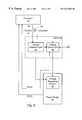
- FIG. 1is a block diagram of one embodiment of a computer system with an electrical over stress protection system
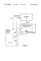
- FIG. 2is a block diagram depicting one embodiment of an over stress protection system (OSPS);
- OSPSover stress protection system
- FIG. 3is a block diagram of an embodiment of the OSPS using a sensed logic signal from a processor
- FIG. 4is a block diagram of an embodiment of the OSPS using a second sensed logic signal from a processor
- FIG. 5is a block diagram of an embodiment of the OSPS using three sensed logic signals from a processor
- FIG. 6is a block diagram of an embodiment of the OSPS using a combination of sensed logic signals from a processor and a signal from a board to which the processor is coupled;
- FIG. 7is a block diagram of one embodiment of a processor shown in FIG. 1;
- FIG. 8is a block diagram of a portion of another embodiment of a computer system.
- FIG. 9is a block diagram of a portion of the OSPS shown in FIG. 8 .
- FIG. 1a block diagram of one embodiment of a computer system with an electrical over stress protection system is shown.
- FIG. 1shows a computer system 200 including an over stress protection system (OSPS) 20 .
- a processor 10coupled to a variety of system components in the computer system 200 through a bus bridge 202 is shown.
- a main memory 204is coupled to bus bridge 202 through a memory bus 206
- a graphics controller 208is coupled to bus bridge 202 through an AGP bus 210 .
- a plurality of PCI devices 212 A- 212 Bare coupled to bus bridge 202 through a PCI bus 214 .
- a secondary bus bridge 216may further be provided to accommodate an electrical interface to one or more EISA or ISA devices 218 through an EISA/ISA bus 220 .
- Processor 10is coupled to bus bridge 202 through bus interface 46 .
- the OSPS 20is coupled to processor 10 and to a power supply 30 .
- Power supply 30is configured to supply voltage to different components within computer system 200 including processor 10 .
- the OSPSmay be coupled to one or more pins of processor 10 or the socket connector pins corresponding to those of the processor pins.
- Bus bridge 202provides an interface between processor 10 , main memory 204 , graphics controller 208 , and devices attached to PCI bus 214 .
- bus bridge 202identifies the target of the operation (e.g. a particular device or, in the case of PCI bus 214 , that the target is on PCI bus 214 ).
- Bus bridge 202routes the operation to the targeted device.
- Bus bridge 202generally translates an operation from the protocol used by the source device or bus to the protocol used by the target device or bus.
- secondary bus bridge 216may further incorporate additional functionality, as desired.
- An input/output controller(not shown), either external from or integrated with secondary bus bridge 216 , may also be included within computer system 200 .
- An external cache unit(not shown) may further be coupled to bus interface 46 between processor 10 and bus bridge 202 in other embodiments.
- the external cachemay be coupled to bus bridge 202 and cache control logic for the external cache may be integrated into bus bridge 202 .
- processor 10may include a “backside cache” configuration in which a separate connection from bus interface 46 is used to connect to an L2 cache. Such a configuration may include the L2 cache and processor 10 incorporated onto a module (e.g. slot 1 or slot A).
- Main memory 204is a memory in which application programs are stored and from which processor 10 primarily executes.
- a suitable main memory 204comprises DRAM (Dynamic Random Access Memory).
- DRAMDynamic Random Access Memory
- SDRAMSerial DRAM
- RDRAMRAMBUS DRAM
- PCI devices 212 A- 212 Bare illustrative of a variety of peripheral devices such as, for example, network interface cards, video accelerators, audio cards, hard or floppy disk drives or drive controllers, SCSI (Small Computer Systems Interface) adapters and telephony cards.
- ISA device 218is illustrative of various types of peripheral devices, such as a modem, a sound card, and a variety of data acquisition cards such as GPIB or field bus interface cards.
- Graphics controller 208is provided to control the rendering of text and images on a display 226 .
- Graphics controller 208may embody a typical graphics accelerator generally known in the art to render three-dimensional data structures which can be effectively shifted into and from main memory 204 .
- Graphics controller 208may therefore be a master of AGP bus 210 in that it can request and receive access to a target interface within bus bridge 202 to thereby obtain access to main memory 204 .
- a dedicated graphics busaccommodates rapid retrieval of data from main memory 204 .
- graphics controller 208may further be configured to generate PCI protocol transactions on AGP bus 210 .
- the AGP interface of bus bridge 202may thus include functionality to support both AGP protocol transactions as well as PCI protocol target and initiator transactions.
- Display 226is any electronic display upon which an image or text can be presented.
- a suitable display 226includes a cathode ray tube (“CRT”), a liquid crystal display (“LCD”), etc.
- CTRcathode ray tube
- LCDliquid crystal display
- computer system 200may be a multiprocessing computer system including additional processors.
- the OSPS 20includes a voltage detection unit 22 and a voltage control unit 24 .
- the voltage detection unit 22is coupled to a processor 10 and the voltage control unit 24 .
- the voltage control unit 24is coupled to a voltage regulating circuitry 40 of power supply 30 .
- the voltage control unit 24is configured to sense a pin of processor 10 wherein processor 10 is equipped with voltage detection capabilities through at least one pin.
- Such a pinmay be the VCC2DET pin 32 shown in FIG. 2 .
- the VCC2DET pin 32may be used to convey a logic signal indicative of a dual voltage requirement or single voltage requirement of the processor.
- the voltage detection unit 22may be additionally configured to sense a second pin of processor 10 .
- the second pincan be used to indicate to the OSPS 20 a level of one of operating voltages of the dual voltages which must be supplied to processor 10 for proper operation upon detection of a dual voltage requirement using the first pin.
- the second pinmay be, for example, the VCC2H/L# pin 34 shown in FIG. 2 .
- the operation of the OSPS 20is performed during the powering up phase of the processor to be connected into a printed circuit board prior to the actual supply of the power to the processor.
- the powermay be supplied by a power supply unit built into the printed circuit board or by an external power supply unit. This step is implemented to insure detection of the voltage requirement prior to actually powering the core and the I/O buffers of the processor to be coupled thereto. Therefore, the OSPS 20 performs its functions prior to actual powering up of the processor.
- the voltage control unit 24 of the OSPS 20(FIG. 2) is configured to control (i.e. enable/disable) the voltage supply to the processor core and I/O buffers.
- Voltage detection unit 22is configured to control the level of voltages supplied to the processor.
- OSPS 20is described as sensing various pins.
- processor 10may be internally configured with either a connection of the sensed pins to ground or no connection.
- an external pullup resistormay be provided upon each sensed pin and detect either a logic low (pin connected to ground) or a logic high (floating pin pulled up by the pullup resistor).
- two pinscould be optionally connected together or not connected together, and the connection/lack of connection could be sensed externally.
- a currentcould be supplied to one of the pins and current sensed at the other pin to detect the connection or lack of connection.
- the sensed pinscould be connected/not connected to a particular pin powered by OSPS 20 during power up. In such an embodiment, pins would be either a logic high (pin connected) or floating (pin not connected) and pulldown resistors may be used.
- a variety of alternativesare contemplated.
- a comparator circuit 510is used to detect two voltage signals from a power supply unit.
- a reference voltagesuch as 3.3 volts
- VCC2core supply voltage
- the comparator 510compares the reference voltage signal with the core voltage signal (VCC2) of the power supply and generates a logic output indicative of the result of the comparison.
- the output signal of comparator 510is a logical one if VCC2 is less than the reference voltage and a logical zero if the VCC2 is greater than the reference voltage.
- the logic output of the comparator 510is exclusively ORed (circuit 520 ) with the logic level sensed on the VCC2DET pin 32 from processor 10 .
- the output of the logic circuit 520is supplied to the power supply regulator circuitry 40 within power supply 30 . If the output is high, voltage regulating circuitry 40 is enabled and processor 10 may be powered up. On the other hand, if the output is low, voltage regulating circuitry 40 is disabled and processor 10 is not powered up.
- processor 10is powered up if: (i) the selected VCC2 (core) voltage is less than the reference voltage and VCC2DET pin 32 is a logical low, indicating dual power supply requirements for processor 10 ; or (ii) the selected VCC2 voltage is greater than the reference voltage and VCC2DET pin 32 is a logical high, indicating single power supply requirements for processor 10 .
- Situation (i)may be indicative of, for example, an AMD-K5TM processor while situation (ii) may be indicative of an AMD-K6® processor in one illustrative example. It is noted that the selected VCC2 voltage may be selected in accordance with the VCC2DET and VCC2H/L# pins as described in more detail below.
- FIG. 4a block diagram of an embodiment of the voltage detection unit 22 is shown wherein a second logic signal sensed from a processor is used as to control the supply voltage level to the processor.
- the VCC2H/L# pin 34is used by voltage detection unit 22 to control voltage regulator 40 .
- the condition of the sensed VCC2H/L# signalis either directly or indirectly used to control the level of a power signal to be supplied to the processor.
- the logic signal on the VCC2H/L# pinis applied into a voltage-divider resistor circuit 26 .
- VCC2H/L#If the VCC2H/L# signal is low (e.g., the pin is internally connected to ground), resistor 630 is bypassed (shorted to ground) and the resulting voltage applied to the processor is reduced to the desired voltage. If the VCC2H/L# signal is not low (for example, the pin is not internally connected to ground), the voltage supplied is developed across the complete resistor circuit ( 610 , 620 , and 630 ) and a higher voltage supply is applied to the processor. The adjustment applied to the voltage supply signal to the processor allows the voltage regulator circuit 40 to apply the correct voltage to the core voltage pins (VCC2 pins) of the processor.
- the processormay be powering up with a different core voltage (e.g., dual-voltage) than the voltage applied to the I/O buffer pins of the processor (whose power may be applied separately from a VCC3 output of the power supply 30 as shown in FIG. 4 ).
- Voltage detection unit 22may not need to provide a pullup resistor on VCC2H/L# pin 34 in this example.
- the OSPS 20is shown where more than two logic signals are detected from a processor to be coupled into a printed circuit board with a range of supply voltages by a power supply.
- the voltage detection unit 22is used to sense logic signals from more than two pins of the processor s to be coupled to the printed circuit board.
- the logic signals detected from a third or more pinsare used to adjust the voltage supplied to the processor through a programmable logic device (PLD) 710 .
- PLDprogrammable logic device
- the voltage detection unit 22Since more logic signals are detected by the voltage detection unit 22 , more options are available due to larger combinations of logic and thus more voltage levels may be adjusted or selected for supply into the processor, thus covering a range of operating voltage requirements for many processors and printed circuit boards.
- at least three logic signalsmay be detected.
- the logic signalsmay be detected from the VCC2DET, VCC2H/L#, and BF1 pins of the processor 10 (reference numerals 32 , 34 , and 36 , respectively).
- the detected logic signalsare supplied to the programmable detection unit 710 prior to the powering up of processor 10 .
- the output of the PLDis used to adjust or select the number and level of voltage supply signals to be supplied into the processor.
- At least one signalis detected from a printed circuit board to which a processor 10 is to be coupled.
- These signals from the printed circuit boardare sampled by the voltage detection unit 22 as additional signals to the logic signals sensed from the processor pins (VCC2DET, VCC2H/L#, and BF1 are shown as reference numerals 32 , 34 , and 36 , respectively).
- signals from jumpers in the printed circuit boardcan be added to the input of the voltage detection unit 22 as illustrated.
- the additional signalsprovide additional options that can be supplied into a voltage control unit or the PLD 710 , thus resulting in a wider range of selection as more voltage control options become available due to more selection options generated from the combination of a larger number of signals.
- processor 10includes a core 64 and one or more I/O buffers 66 . Additionally, processor 10 includes VCC2DET pin 32 and VCC2H/L# pin 34 (as well as other pins used by I/O buffers 66 for communication, not shown).
- the core voltage (VCC2)is illustrated by a pin 62 . However, it is noted that multiple pins may be used to supply the core voltage.
- the I/O voltage (VCC3)is shown as a pin 60 . However, it is noted that multiple pins may be used to supply the I/O voltage.
- core 64includes the logic circuitry employed to perform the functions of processor 10
- I/O buffers 66include the circuitry for communicating with other devices (e.g. using bus interface 46 ).
- the core voltage provided on VCC2 pin(s) 62powers the circuitry in core 64
- the I/O voltage provided on VCC3 pin(s) 60powers the I/O buffer circuitry in I/O buffers 66 .
- FIG. 8a block diagram of a portion of another embodiment of a computer system (computer system 200 a ) is shown.
- a processor 10 ais coupled to an OSPS 20 a , a power supply 30 a , a clock unit 74 , bus bridge 202 , and an optional cache 72 .
- processor 10 ais coupled to OSPS 20 a via VCC2DET pin 32 , VCC2H/L# pin 34 , BF1 pin 36 , and a VCC18 pin 70 .
- processor 10 areceives a core voltage supply VCC2 and an I/O voltage supply VCC3 from power supply 30 a .
- Processor 10 ais configured to receive a clock signal from clock unit 74 and is coupled to communicate via bus interface 46 with bus bridge 202 and cache 72 .
- Processor 10 ais configured to indicate its dual voltage requirements using VCC2DET pin 32 , as described above for processor 10 . Furthermore, processor 10 a is configured to indicate a high or low voltage level requirement for VCC2 via the VCC2H/L# pin 34 similar to the above description. However, processor 10 a may require an even lower VCC2 voltage than processor 10 (e.g. 1.8 volts). Furthermore, processor 10 a requires that VCC3 be lower than that required by processor 10 (e.g. 2.5 volts). Processor 10 a indicates these lower voltage requirements using VCC18 pin 70 .
- VCC18 pin 70is either internally not connected or internally connected to ground.
- An external pullup resistormay be used to pull up VCC18 pin 70 similar to VCC2DET and VCC2H/L# pins 32 and 34 .
- pullup resistorsmay be eliminated with an appropriate voltage detection unit.
- Alternative connections for VCC18 pin 70are possible as well, similar to the above description of the VCC2DET and VCC2H/L# pins.
- OSPS 20 acontrols power supply 30 a to provide power to processor 10 a and to other devices shown in FIG. 8 .
- the VCC2 voltageis generated in response to both the VCC2H/L# and VCC18 pins. For example, in one exemplary embodiment, if VCC2H/L# pin 32 is floating and VCC18 pin 70 is floating, then VCC2 may be supplied at 2.9 volts. If VCC2H/L# pin 32 is a logic low and VCC18 pin 70 is floating, then VCC2 may be supplied at 2.2 volts.
- VCC18is a logic low
- VCC2H/L# pin 32is a don't care and VCC2 may be supplied at 1.8 volts.
- Other voltage levelsmay be selected in other embodiments, according to the requirements of the particular processor, and the VCC2H/L# pin and VCC18 pin may be used to select between a high, medium, and low voltage level from among the desired voltage levels.
- the generated VCC2 voltageis provided to the VCC2 pin(s) of processor 10 a.
- Power supply 30 afurther generates a VIO voltage responsive to VCC18 pin 70 .
- the VIO voltageis supplied to the VCC3 pin(s) of processor 10 a , and is the voltage supplied to the I/O buffers of other devices which communicate with processor 10 a (or at least those I/O buffers coupled to pins of processor 10 a ). In this manner, all devices coupled to processor 10 a may employ voltage levels compatible with processor 10 a .
- the processor I/O sections of clock unit 74 , bus bridge 202 , and cache 72are powered by the VIO voltage.
- remaining portions of theses devicesmay be powered with a VSYS voltage (e.g. 3.3 volts) provided by power supply 30 a.
- VSYS voltagee.g. 3.3 volts
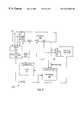
- FIG. 9a block diagram illustrating processor 10 a , power supply 30 a , and portions of OSPS 20 a is shown. Other embodiments are possible and contemplated.
- voltage detection units 22 A and 22 Bare shown. Voltage detection units 22 A and 22 B, in addition to a voltage control unit 24 described above, may comprise one embodiment of OSPS 20 a.
- Voltage detection unit 22 Amay operate in conjunction with voltage regulating circuitry 40 A to produce the VIO voltage from power supply 30 a .
- voltage detection unit 22 Acomprises a voltage divider circuit including resistors 810 , 820 , and 830 connected in series.
- VCC18 pin 70is coupled to the node between resistors 810 and 820 . Accordingly, if VCC18 is connected to ground, then resistor 810 is bypassed (i.e. shorted). The VIO voltage is therefore lowered to the desired lower voltage level (e.g. 2.5 volts). On the other hand, if VCC18 is floating, the VIO voltage is developed across the entire set of resistors 810 - 830 , and a higher VIO voltage is generated (e.g. 3.3. volts).
- Voltage detection unit 22 Bcontrols voltage regulating circuitry 40 B to generate the VCC2 voltage as one of three possible voltage levels in response to the VCC18 pin 70 and the VCC2H/L# pin 34 .
- Voltage detection unit 22 Bcomprises a voltage divider circuit including resistors 840 , 850 , 860 , and 870 connected in series.
- VCC18 pin 70is coupled to the node between resistors 860 and 850
- VCC2H/L# pin 34is coupled to the node between resistors 840 and 850 .
- VCC2H/L# pin 34 and VCC18 pin 70are floating, the VCC2 voltage is developed across the entire set of resistors 840 - 870 and the highest voltage deliverable by voltage regulating circuitry 40 B and voltage detection unit 22 B is provided (e.g. 2.9 volts).
- resistor 840is shorted and the VCC2 voltage is lowered (e.g. to 2.2 volts).
- VCC18 pin 70is connected to ground, both resistors 840 and 850 are shorted and the VCC2 voltage is lowered even further (e.g. to 1.8 volts).
- voltage regulating circuitry 40 A- 40 Bmay comprise any suitable voltage regulator (e.g. linear regulators or DC/DC converters).
- voltage regulating circuitry 40 Amay comprise a linear regulator and voltage regulator circuitry 40 B may comprise a linear regulator or DC/DC converter.
- any suitable valuesmay be selected for resistors 610 - 630 (shown in FIG. 4) and 810 - 870 (shown in FIG. 9 ). Generally, the resistance of each of resistors 610 - 630 is selected to supply the desired higher VCC2 voltage when resistor 630 is not shorted and the desired lower VCC2 voltage when resistor 630 is shorted.
- each of resistors 810 - 830is selected to supply the desired higher VIO voltage when resistor 810 is not shorted and the desired lower VIO voltage when resistor 810 is shorted.
- the resistance of each of resistors 840 - 870is selected to supply the desired highest VCC2 voltage when resistors 840 and 850 are not shorted, the desired medium VCC2 voltage when resistor 840 is shorted by 850 is not shorted, and the desired lower VCC2 voltage when resistors 840 and 850 are both shorted.
- the ability to indicate and adjust voltage levels in the manner shownmay be extended to any desired number of voltage selections by employing additional pins in an encoded or non-encoded format.
- processors 10 and 10 aare described herein as being coupled to other circuits (e.g. OSPS 20 , power supply 30 , etc.).
- the pinsmay be coupled, for example, either directly or indirectly through wiring on the printed circuit board or other electrical coupling to the receiving devices.
- pin nameshave been used corresponding to an illustrative embodiment corresponding to an AMD-K6® processor, the pin names are not meant to be restrictive. Any pins may be selected in any type of processor for providing automatic voltage detection in accordance with the present disclosure. Furthermore, multiple pins may be used to indicate more than two possible voltage levels for VCC2, or even VCC3, as desired.
Landscapes
- Engineering & Computer Science (AREA)
- Theoretical Computer Science (AREA)
- Physics & Mathematics (AREA)
- General Engineering & Computer Science (AREA)
- General Physics & Mathematics (AREA)
- Power Sources (AREA)
Abstract
Description
Claims (10)
Priority Applications (1)
| Application Number | Priority Date | Filing Date | Title |
|---|---|---|---|
| US09/176,737US6327663B2 (en) | 1998-10-21 | 1998-10-21 | System and method for processor dual voltage detection and over stress protection |
Applications Claiming Priority (1)
| Application Number | Priority Date | Filing Date | Title |
|---|---|---|---|
| US09/176,737US6327663B2 (en) | 1998-10-21 | 1998-10-21 | System and method for processor dual voltage detection and over stress protection |
Publications (2)
| Publication Number | Publication Date |
|---|---|
| US20010001878A1 US20010001878A1 (en) | 2001-05-24 |
| US6327663B2true US6327663B2 (en) | 2001-12-04 |
Family
ID=22645636
Family Applications (1)
| Application Number | Title | Priority Date | Filing Date |
|---|---|---|---|
| US09/176,737Expired - LifetimeUS6327663B2 (en) | 1998-10-21 | 1998-10-21 | System and method for processor dual voltage detection and over stress protection |
Country Status (1)
| Country | Link |
|---|---|
| US (1) | US6327663B2 (en) |
Cited By (25)
| Publication number | Priority date | Publication date | Assignee | Title |
|---|---|---|---|---|
| US20020120882A1 (en)* | 2000-12-22 | 2002-08-29 | Ananda Sarangi | Dynamic processor configuration and power-up |
| US20020162040A1 (en)* | 2001-04-30 | 2002-10-31 | Zhang Michael T. | Supply voltage identification |
| US6574577B2 (en)* | 2000-12-13 | 2003-06-03 | Intel Corporation | Circuit to indicate the status of a supply voltage |
| US6615360B1 (en)* | 2000-01-25 | 2003-09-02 | International Business Machines Corporation | Method and system for controlling a power on sequence in response to monitoring respective components of a computer system with multiple CPU sockets to determine proper functionality |
| US6651178B1 (en)* | 2000-02-29 | 2003-11-18 | 3Com Corporation | Communication module having power supply requirement identification |
| US20040075703A1 (en)* | 2002-10-17 | 2004-04-22 | Cronch Darell D. | Switching power supply, method of operation and device-and-power-supply assembly |
| US20040117673A1 (en)* | 2002-12-17 | 2004-06-17 | Tawfik Arabi | Method and apparatus to provide platform load lines |
| US20040123163A1 (en)* | 2002-12-20 | 2004-06-24 | Ta-Feng Huang | Device for managing electric power source of CPU |
| US20050050235A1 (en)* | 2003-09-02 | 2005-03-03 | Soo-Hwan Choi | System having insertable and removable storage and a control method thereof |
| US20050071696A1 (en)* | 2003-09-30 | 2005-03-31 | Pearl Lowell Raymond | Providing a low-power state processor voltage in accordance with a detected processor type |
| US20050086434A1 (en)* | 2003-10-02 | 2005-04-21 | Kang Sang-Wook | Multimedia/secure digital cards and adapters for interfacing to hosts and methods of operating |
| US20050088155A1 (en)* | 2003-10-23 | 2005-04-28 | Osburn Edward P. | Multi-sense voltage regulator |
| US20050102043A1 (en)* | 2003-11-07 | 2005-05-12 | Menas Gregory W. | Automatic sensing power systems and methods |
| US6978388B1 (en)* | 2002-01-18 | 2005-12-20 | Apple Computer, Inc. | Method and apparatus for managing a power load change in a system |
| US6985987B2 (en)* | 2000-11-01 | 2006-01-10 | Via Technologies, Inc. | Apparatus and method for supporting multi-processors and motherboard of the same |
| US20060179330A1 (en)* | 2005-01-27 | 2006-08-10 | Ziarnik Gregory P | Apparatus and method for ensuring power compatibility between a system board and a processing device |
| US20070174698A1 (en)* | 2005-12-22 | 2007-07-26 | International Business Machines Corporation | Methods and apparatuses for supplying power to processors in multiple processor systems |
| US20070206422A1 (en)* | 2006-03-01 | 2007-09-06 | Roohparvar Frankie F | Nand memory device column charging |
| US20080276026A1 (en)* | 2007-05-02 | 2008-11-06 | Advanced Micro Devices, Inc. | Selective deactivation of processor cores in multiple processor core systems |
| US7745954B1 (en) | 2007-01-15 | 2010-06-29 | Polsinelli Shughart PC | Power sampling systems and methods |
| US20110012561A1 (en)* | 2009-07-16 | 2011-01-20 | John Whiting | Battery charger with automatic voltage detection |
| US20110169562A1 (en)* | 2010-01-08 | 2011-07-14 | Mindspeed Technologies, Inc. | System on chip power management through package configuration |
| US8296587B2 (en) | 2006-08-30 | 2012-10-23 | Green Plug, Inc. | Powering an electrical device through a legacy adapter capable of digital communication |
| US20130067250A1 (en)* | 2011-09-08 | 2013-03-14 | Asustek Computer Inc. | Computer device and frequency adjusting method for central processing unit |
| US20160335095A1 (en)* | 2015-05-11 | 2016-11-17 | Hong Fu Jin Precision Industry (Shenzhen) Co., Ltd | Booting system |
Families Citing this family (6)
| Publication number | Priority date | Publication date | Assignee | Title |
|---|---|---|---|---|
| TW438198U (en)* | 1999-10-14 | 2001-05-28 | Via Tech Inc | Wiring structure of a printed circuit board |
| JP5358370B2 (en)* | 2009-09-18 | 2013-12-04 | 株式会社キーエンス | Optical information reader |
| US20130086395A1 (en)* | 2011-09-30 | 2013-04-04 | Qualcomm Incorporated | Multi-Core Microprocessor Reliability Optimization |
| US8996902B2 (en) | 2012-10-23 | 2015-03-31 | Qualcomm Incorporated | Modal workload scheduling in a heterogeneous multi-processor system on a chip |
| CN107589773B (en)* | 2017-09-05 | 2019-01-22 | 华大半导体有限公司 | Super low-power consumption High-reliability power source management design and implementation method |
| CN107562106B (en)* | 2017-09-05 | 2019-01-22 | 华大半导体有限公司 | A kind of super low-power consumption High-reliability power source management design and implementation method |
Citations (11)
| Publication number | Priority date | Publication date | Assignee | Title |
|---|---|---|---|---|
| US5546563A (en) | 1991-04-22 | 1996-08-13 | Acer Incorporated | Single chip replacement upgradeable computer motherboard with enablement of inserted upgrade CPU chip |
| US5551012A (en) | 1991-04-22 | 1996-08-27 | Acer Incorporated | Single socket upgradeable computer motherboard with automatic detection and socket reconfiguration for inserted CPU chip |
| US5613130A (en) | 1994-11-10 | 1997-03-18 | Vadem Corporation | Card voltage switching and protection |
| US5757171A (en)* | 1996-12-31 | 1998-05-26 | Intel Corporation | On-board voltage regulators with automatic processor type detection |
| US5862351A (en)* | 1996-11-07 | 1999-01-19 | He; Zhi Qiang | Motherboard with automatic configuration |
| US5864225A (en)* | 1997-06-04 | 1999-01-26 | Fairchild Semiconductor Corporation | Dual adjustable voltage regulators |
| US5939868A (en)* | 1996-03-29 | 1999-08-17 | Intel Corporation | Method and apparatus for automatically controlling integrated circuit supply voltages |
| US5943227A (en)* | 1996-06-26 | 1999-08-24 | Fairchild Semiconductor Corporation | Programmable synchronous step down DC-DC converter controller |
| US5951681A (en)* | 1997-12-01 | 1999-09-14 | Micro-Star International Co., Ltd. | Method and device of plugging and immediately playing a CPU |
| US6035407A (en)* | 1995-08-14 | 2000-03-07 | Compaq Computer Corporation | Accomodating components |
| US6058030A (en)* | 1997-11-20 | 2000-05-02 | Intersil Corporation | Multiple output DC-to-DC converter having enhanced noise margin and related methods |
- 1998
- 1998-10-21USUS09/176,737patent/US6327663B2/ennot_activeExpired - Lifetime
Patent Citations (11)
| Publication number | Priority date | Publication date | Assignee | Title |
|---|---|---|---|---|
| US5546563A (en) | 1991-04-22 | 1996-08-13 | Acer Incorporated | Single chip replacement upgradeable computer motherboard with enablement of inserted upgrade CPU chip |
| US5551012A (en) | 1991-04-22 | 1996-08-27 | Acer Incorporated | Single socket upgradeable computer motherboard with automatic detection and socket reconfiguration for inserted CPU chip |
| US5613130A (en) | 1994-11-10 | 1997-03-18 | Vadem Corporation | Card voltage switching and protection |
| US6035407A (en)* | 1995-08-14 | 2000-03-07 | Compaq Computer Corporation | Accomodating components |
| US5939868A (en)* | 1996-03-29 | 1999-08-17 | Intel Corporation | Method and apparatus for automatically controlling integrated circuit supply voltages |
| US5943227A (en)* | 1996-06-26 | 1999-08-24 | Fairchild Semiconductor Corporation | Programmable synchronous step down DC-DC converter controller |
| US5862351A (en)* | 1996-11-07 | 1999-01-19 | He; Zhi Qiang | Motherboard with automatic configuration |
| US5757171A (en)* | 1996-12-31 | 1998-05-26 | Intel Corporation | On-board voltage regulators with automatic processor type detection |
| US5864225A (en)* | 1997-06-04 | 1999-01-26 | Fairchild Semiconductor Corporation | Dual adjustable voltage regulators |
| US6058030A (en)* | 1997-11-20 | 2000-05-02 | Intersil Corporation | Multiple output DC-to-DC converter having enhanced noise margin and related methods |
| US5951681A (en)* | 1997-12-01 | 1999-09-14 | Micro-Star International Co., Ltd. | Method and device of plugging and immediately playing a CPU |
Non-Patent Citations (11)
| Title |
|---|
| "AMD-K6, MMx Enhanced Processor," Data Sheet, Advanced Micro Devices, Inc., Sep. 1997, 10 pages. |
| AMD-K6 Processor Data Sheet, Mr. 1998.* |
| AMD-K6 Processor, "Vcc2 Voltage Detection," May 1998 Advanced Micro Devices, Inc., 12 pages. |
| Application Note: AMD-K5(TM): Support for the AMD-K5 Dual Voltage Processor, Publication #19766, Rev: C, Issue Date: Sep. 1996, pp. 1-18. |
| Application Note: AMD-K5™: Support for the AMD-K5 Dual Voltage Processor, Publication #19766, Rev: C, Issue Date: Sep. 1996, pp. 1-18. |
| Application Note: intel(R) Pentium(R) Processor Flexible Motherboard Design Guidelines, AP-579, Order No: 243187-002, Jun. 1997, pp. 1-54. |
| Application Note: intel(R) Voltage Guidelines for Pentium(R) Processors with MMX(TM) Technology, AP-580, Order No.: 243186-003, Jun. 1997, 1-30. |
| Application Note: intel® Pentium® Processor Flexible Motherboard Design Guidelines, AP-579, Order No: 243187-002, Jun. 1997, pp. 1-54. |
| Application Note: intel® Voltage Guidelines for Pentium® Processors with MMX™ Technology, AP-580, Order No.: 243186-003, Jun. 1997, 1-30. |
| intel(R) Pentium(R) Pro Processor at 150 MHz, 166 MHz, 180 MHz And 200 MHz, Order No.: 242769-003, Feb. 1996, 3 pages. |
| intel® Pentium® Pro Processor at 150 MHz, 166 MHz, 180 MHz And 200 MHz, Order No.: 242769-003, Feb. 1996, 3 pages. |
Cited By (80)
| Publication number | Priority date | Publication date | Assignee | Title |
|---|---|---|---|---|
| US6615360B1 (en)* | 2000-01-25 | 2003-09-02 | International Business Machines Corporation | Method and system for controlling a power on sequence in response to monitoring respective components of a computer system with multiple CPU sockets to determine proper functionality |
| US6651178B1 (en)* | 2000-02-29 | 2003-11-18 | 3Com Corporation | Communication module having power supply requirement identification |
| US6985987B2 (en)* | 2000-11-01 | 2006-01-10 | Via Technologies, Inc. | Apparatus and method for supporting multi-processors and motherboard of the same |
| US6574577B2 (en)* | 2000-12-13 | 2003-06-03 | Intel Corporation | Circuit to indicate the status of a supply voltage |
| US20020120882A1 (en)* | 2000-12-22 | 2002-08-29 | Ananda Sarangi | Dynamic processor configuration and power-up |
| US6874083B2 (en)* | 2000-12-22 | 2005-03-29 | Intel Corporation | Method and apparatus to ensure proper voltage and frequency configuration signals are defined before applying power to processor |
| US6823465B2 (en)* | 2001-04-30 | 2004-11-23 | Intel Corporation | Establishment of voltage of a terminal at a voltage level in response to validating the indication of the voltage to be supplied to the terminal |
| US20020162040A1 (en)* | 2001-04-30 | 2002-10-31 | Zhang Michael T. | Supply voltage identification |
| US6978388B1 (en)* | 2002-01-18 | 2005-12-20 | Apple Computer, Inc. | Method and apparatus for managing a power load change in a system |
| US20060123256A1 (en)* | 2002-01-18 | 2006-06-08 | Cornelius William P | Method and apparatus for managing a power load change in a system |
| US7437586B2 (en)* | 2002-01-18 | 2008-10-14 | Apple Inc. | Method and apparatus for managing a power load change in a system |
| US7227652B2 (en) | 2002-10-17 | 2007-06-05 | Lexmark International, Inc. | Switching power supply, method of operation and device-and-power-supply assembly |
| US20040075703A1 (en)* | 2002-10-17 | 2004-04-22 | Cronch Darell D. | Switching power supply, method of operation and device-and-power-supply assembly |
| US20040117673A1 (en)* | 2002-12-17 | 2004-06-17 | Tawfik Arabi | Method and apparatus to provide platform load lines |
| US20040123163A1 (en)* | 2002-12-20 | 2004-06-24 | Ta-Feng Huang | Device for managing electric power source of CPU |
| US20050050235A1 (en)* | 2003-09-02 | 2005-03-03 | Soo-Hwan Choi | System having insertable and removable storage and a control method thereof |
| US7617335B2 (en)* | 2003-09-02 | 2009-11-10 | Samsung Electronics Co., Ltd. | System having insertable and removable storage and a control method thereof |
| US20050071696A1 (en)* | 2003-09-30 | 2005-03-31 | Pearl Lowell Raymond | Providing a low-power state processor voltage in accordance with a detected processor type |
| US7200762B2 (en)* | 2003-09-30 | 2007-04-03 | Intel Corporation | Providing a low-power state processor voltage in accordance with a detected processor type |
| US20050086434A1 (en)* | 2003-10-02 | 2005-04-21 | Kang Sang-Wook | Multimedia/secure digital cards and adapters for interfacing to hosts and methods of operating |
| US7237049B2 (en)* | 2003-10-02 | 2007-06-26 | Samsung Electronics Co., Ltd. | Multimedia/secure digital cards and adapters for interfacing using voltage levels to determine host types and methods of operating |
| US7102338B2 (en)* | 2003-10-23 | 2006-09-05 | Intel Corporation | Multi-sense voltage regulator |
| US20050088155A1 (en)* | 2003-10-23 | 2005-04-28 | Osburn Edward P. | Multi-sense voltage regulator |
| US7514814B2 (en) | 2003-11-07 | 2009-04-07 | Mpathx, Llc | Automatic sensing power systems and methods |
| US7508092B2 (en) | 2003-11-07 | 2009-03-24 | Mpathx, Llc | Automatic sensing power systems and methods |
| US20060202557A1 (en)* | 2003-11-07 | 2006-09-14 | Mpathx, Llc | Automatic sensing power systems and methods |
| US7816807B2 (en) | 2003-11-07 | 2010-10-19 | Menas Gregory W | Automatic sensing power systems and methods |
| US20060129252A1 (en)* | 2003-11-07 | 2006-06-15 | Mpathx, Llc | Automatic sensing power systems and methods |
| US20060129253A1 (en)* | 2003-11-07 | 2006-06-15 | Mpathx, Llc | Automatic sensing power systems and methods |
| US7242111B2 (en) | 2003-11-07 | 2007-07-10 | Mpathx, Llc | Automatic sensing power systems and methods |
| US7812477B2 (en) | 2003-11-07 | 2010-10-12 | Menas Gregory W | Automatic sensing power systems and methods |
| US8115335B2 (en) | 2003-11-07 | 2012-02-14 | Green Plug, Inc. | Automatic sensing power systems and methods |
| US7285874B2 (en) | 2003-11-07 | 2007-10-23 | Mpathx, Llc | Automatic sensing power systems and methods |
| US20070257559A1 (en)* | 2003-11-07 | 2007-11-08 | Mpathx, Llc | Automatic Sensing Power Systems and Methods |
| US20070273208A1 (en)* | 2003-11-07 | 2007-11-29 | Mpathx, Llc | Automatic Sensing Power Systems and Methods |
| US7960859B2 (en) | 2003-11-07 | 2011-06-14 | Green Plug, Inc. | Automatic sensing power systems and methods |
| US20060119993A1 (en)* | 2003-11-07 | 2006-06-08 | Mpathx, Llc | Automatic sensing power systems and methods |
| US20110018345A1 (en)* | 2003-11-07 | 2011-01-27 | Polsinelli Shughart PC | Automatic Sensing Power Systems and Methods |
| US7485986B2 (en) | 2003-11-07 | 2009-02-03 | Mpathx, Llc | Automatic sensing power systems and methods |
| US20060183510A1 (en)* | 2003-11-07 | 2006-08-17 | Mpathx, Llc | Automatic sensing power systems and methods |
| US7816809B2 (en) | 2003-11-07 | 2010-10-19 | Menas Gregory W | Automatic sensing power systems and methods |
| US20060119182A1 (en)* | 2003-11-07 | 2006-06-08 | Mpathx, Llc | Automatic sensing power systems and methods |
| US7812475B2 (en) | 2003-11-07 | 2010-10-12 | Menas Gregory W | Automatic sensing power systems and methods |
| US7579711B2 (en) | 2003-11-07 | 2009-08-25 | Mpathx, Llc | Automatic sensing power systems and methods |
| US7602079B2 (en) | 2003-11-07 | 2009-10-13 | Mpathx, Llc | Automatic sensing power systems and methods |
| US20050102043A1 (en)* | 2003-11-07 | 2005-05-12 | Menas Gregory W. | Automatic sensing power systems and methods |
| US7646111B2 (en) | 2003-11-07 | 2010-01-12 | Mpathx, Llc | Automatic sensing power systems and methods |
| US7816810B2 (en) | 2003-11-07 | 2010-10-19 | Menas Gregory W | Automatic sensing power systems and methods |
| US7768152B2 (en) | 2003-11-07 | 2010-08-03 | Mpathx, Llc | Automatic sensing power systems and methods |
| US7816808B2 (en) | 2003-11-07 | 2010-10-19 | Menas Gregory W | Automatic sensing power systems and methods |
| US7791220B2 (en) | 2003-11-07 | 2010-09-07 | Polsinelli Shughart PC | Automatic sensing power systems and methods |
| US7808122B2 (en) | 2003-11-07 | 2010-10-05 | Menas Gregory W | Automatic sensing power systems and methods |
| US7812476B2 (en) | 2003-11-07 | 2010-10-12 | Menas Gregory W | Automatic sensing power systems and methods |
| US20060179330A1 (en)* | 2005-01-27 | 2006-08-10 | Ziarnik Gregory P | Apparatus and method for ensuring power compatibility between a system board and a processing device |
| US7526674B2 (en)* | 2005-12-22 | 2009-04-28 | International Business Machines Corporation | Methods and apparatuses for supplying power to processors in multiple processor systems |
| US20070174698A1 (en)* | 2005-12-22 | 2007-07-26 | International Business Machines Corporation | Methods and apparatuses for supplying power to processors in multiple processor systems |
| US20090034331A1 (en)* | 2006-03-01 | 2009-02-05 | Micron Technology, Inc. | Nand memory device column charging |
| US8040732B2 (en) | 2006-03-01 | 2011-10-18 | Micron Technology, Inc. | NAND memory device column charging |
| US7782677B2 (en) | 2006-03-01 | 2010-08-24 | Micron Technology, Inc. | NAND memory device column charging |
| US20100296346A1 (en)* | 2006-03-01 | 2010-11-25 | Roohparvar Frankie F | Nand memory device column charging |
| US20070206422A1 (en)* | 2006-03-01 | 2007-09-06 | Roohparvar Frankie F | Nand memory device column charging |
| US7436708B2 (en) | 2006-03-01 | 2008-10-14 | Micron Technology, Inc. | NAND memory device column charging |
| US8296587B2 (en) | 2006-08-30 | 2012-10-23 | Green Plug, Inc. | Powering an electrical device through a legacy adapter capable of digital communication |
| US7812479B1 (en) | 2007-01-15 | 2010-10-12 | Menas Gregory W | Power sampling systems and methods |
| US7745954B1 (en) | 2007-01-15 | 2010-06-29 | Polsinelli Shughart PC | Power sampling systems and methods |
| US7812478B1 (en) | 2007-01-15 | 2010-10-12 | Menas Gregory W | Power sampling systems and methods |
| US7856562B2 (en)* | 2007-05-02 | 2010-12-21 | Advanced Micro Devices, Inc. | Selective deactivation of processor cores in multiple processor core systems |
| US20080276026A1 (en)* | 2007-05-02 | 2008-11-06 | Advanced Micro Devices, Inc. | Selective deactivation of processor cores in multiple processor core systems |
| US9529052B2 (en) | 2009-07-16 | 2016-12-27 | Schumacher Electric Corporation | Battery charger with automatic voltage detection |
| US20110012561A1 (en)* | 2009-07-16 | 2011-01-20 | John Whiting | Battery charger with automatic voltage detection |
| US8575899B2 (en)* | 2009-07-16 | 2013-11-05 | Schumacher Electric Corporation | Battery charger with automatic voltage detection |
| US20140021906A1 (en)* | 2009-07-16 | 2014-01-23 | Schumacher Electric Corporation | Battery charger with automatic voltage detection |
| US8922172B2 (en)* | 2009-07-16 | 2014-12-30 | Schumacher Electric Corporation | Battery charger with automatic voltage detection |
| US9874611B2 (en) | 2009-07-16 | 2018-01-23 | Schumacher Electric Corporation | Battery charger with automatic voltage detection |
| US20110169562A1 (en)* | 2010-01-08 | 2011-07-14 | Mindspeed Technologies, Inc. | System on chip power management through package configuration |
| US8717093B2 (en)* | 2010-01-08 | 2014-05-06 | Mindspeed Technologies, Inc. | System on chip power management through package configuration |
| US20130067250A1 (en)* | 2011-09-08 | 2013-03-14 | Asustek Computer Inc. | Computer device and frequency adjusting method for central processing unit |
| US8972754B2 (en)* | 2011-09-08 | 2015-03-03 | Asustek Computer Inc. | Computer device and frequency adjusting method for central processing unit |
| US20160335095A1 (en)* | 2015-05-11 | 2016-11-17 | Hong Fu Jin Precision Industry (Shenzhen) Co., Ltd | Booting system |
| US9626195B2 (en)* | 2015-05-11 | 2017-04-18 | Hong Fu Jin Precision Industry (Shenzhen) Co., Ltd. | Booting system |
Also Published As
| Publication number | Publication date |
|---|---|
| US20010001878A1 (en) | 2001-05-24 |
Similar Documents
| Publication | Publication Date | Title |
|---|---|---|
| US6327663B2 (en) | System and method for processor dual voltage detection and over stress protection | |
| US5757171A (en) | On-board voltage regulators with automatic processor type detection | |
| US6535944B1 (en) | Hot plug control of MP based computer system | |
| US6339831B1 (en) | Automatic detecting unit for diagnosing a connection and identifying an external device, information processing apparatus, and external device | |
| EP1163571B1 (en) | Add-on card with automatic bus power line selection circuit | |
| US7099481B2 (en) | Method and system for automatically detecting and powering PC speakers | |
| US20030172312A1 (en) | USB device | |
| US20080048665A1 (en) | Generation of System Power-Good Signal in Hot-Swap Power Controllers | |
| EP0892945A1 (en) | Method and apparatus for automatically controlling intergrated circuit supply voltages | |
| EP0932097A1 (en) | Bus controllers ensuring reduced power consumption and stable operation | |
| US11333716B2 (en) | Electronic device and power receiving control method thereof | |
| US6094367A (en) | Voltage regulating device for dynamically regulating voltage in a computer system | |
| US8312298B2 (en) | PXI express controller power control state machine | |
| HK1041540B (en) | Method and apparatus for maintaining load balance on a graphics bus when an upgrade device is installed | |
| JP3673239B2 (en) | Computer equipment | |
| US6640273B1 (en) | Apparatus for data bus expansion between two instrument chassis | |
| US7216241B2 (en) | Self-testing power supply which indicates when an output voltage is within tolerance while not coupled to an external load | |
| US11288224B2 (en) | Semiconductor system and semiconductor device | |
| US20040210777A1 (en) | Method and apparatus for enhanced power consumption handling of bus-controlled components | |
| TW201737236A (en) | Method for reading identification data from display and associated processing circuit | |
| US6530048B1 (en) | I2C test single chip | |
| US6721150B1 (en) | Clamping circuit for use in computer system | |
| US6154067A (en) | Methods of and apparatus for monitoring the termination status of a SCSI bus | |
| US8041846B2 (en) | Apparatus with reduced latency for master and slave storage devices | |
| US5986352A (en) | Smart peripheral back-power prevention |
Legal Events
| Date | Code | Title | Description |
|---|---|---|---|
| AS | Assignment | Owner name:ADVANCED MICRO DEVICES, INC., CALIFORNIA Free format text:ASSIGNMENT OF ASSIGNORS INTEREST;ASSIGNORS:ISAAC, GERALD G.;CALDWELL, DERVINN D.;SMITH, LANCE L.;AND OTHERS;REEL/FRAME:009539/0807 Effective date:19981015 | |
| STCF | Information on status: patent grant | Free format text:PATENTED CASE | |
| FEPP | Fee payment procedure | Free format text:PAYOR NUMBER ASSIGNED (ORIGINAL EVENT CODE: ASPN); ENTITY STATUS OF PATENT OWNER: LARGE ENTITY | |
| FPAY | Fee payment | Year of fee payment:4 | |
| FPAY | Fee payment | Year of fee payment:8 | |
| AS | Assignment | Owner name:GLOBALFOUNDRIES INC., CAYMAN ISLANDS Free format text:ASSIGNMENT OF ASSIGNORS INTEREST;ASSIGNOR:AMD TECHNOLOGIES HOLDINGS, INC.;REEL/FRAME:022764/0544 Effective date:20090302 Owner name:AMD TECHNOLOGIES HOLDINGS, INC., CALIFORNIA Free format text:ASSIGNMENT OF ASSIGNORS INTEREST;ASSIGNOR:ADVANCED MICRO DEVICES, INC.;REEL/FRAME:022764/0488 Effective date:20090302 | |
| FPAY | Fee payment | Year of fee payment:12 | |
| AS | Assignment | Owner name:WILMINGTON TRUST, NATIONAL ASSOCIATION, DELAWARE Free format text:SECURITY AGREEMENT;ASSIGNOR:GLOBALFOUNDRIES INC.;REEL/FRAME:049490/0001 Effective date:20181127 | |
| AS | Assignment | Owner name:GLOBALFOUNDRIES INC., CAYMAN ISLANDS Free format text:RELEASE BY SECURED PARTY;ASSIGNOR:WILMINGTON TRUST, NATIONAL ASSOCIATION;REEL/FRAME:054636/0001 Effective date:20201117 | |
| AS | Assignment | Owner name:GLOBALFOUNDRIES U.S. INC., NEW YORK Free format text:RELEASE BY SECURED PARTY;ASSIGNOR:WILMINGTON TRUST, NATIONAL ASSOCIATION;REEL/FRAME:056987/0001 Effective date:20201117 |