US6327639B1 - Method and apparatus for storing location identification information within non-volatile memory devices - Google Patents
Method and apparatus for storing location identification information within non-volatile memory devicesDownload PDFInfo
- Publication number
- US6327639B1 US6327639B1US09/580,392US58039200AUS6327639B1US 6327639 B1US6327639 B1US 6327639B1US 58039200 AUS58039200 AUS 58039200AUS 6327639 B1US6327639 B1US 6327639B1
- Authority
- US
- United States
- Prior art keywords
- buffer
- primary
- storing
- lba
- information
- Prior art date
- Legal status (The legal status is an assumption and is not a legal conclusion. Google has not performed a legal analysis and makes no representation as to the accuracy of the status listed.)
- Expired - Lifetime
Links
Images


Classifications
- G—PHYSICS
- G06—COMPUTING OR CALCULATING; COUNTING
- G06F—ELECTRIC DIGITAL DATA PROCESSING
- G06F3/00—Input arrangements for transferring data to be processed into a form capable of being handled by the computer; Output arrangements for transferring data from processing unit to output unit, e.g. interface arrangements
- G06F3/06—Digital input from, or digital output to, record carriers, e.g. RAID, emulated record carriers or networked record carriers
- G06F3/0601—Interfaces specially adapted for storage systems
- G06F3/0602—Interfaces specially adapted for storage systems specifically adapted to achieve a particular effect
- G06F3/061—Improving I/O performance
- G06F3/0613—Improving I/O performance in relation to throughput
- G—PHYSICS
- G06—COMPUTING OR CALCULATING; COUNTING
- G06F—ELECTRIC DIGITAL DATA PROCESSING
- G06F12/00—Accessing, addressing or allocating within memory systems or architectures
- G06F12/02—Addressing or allocation; Relocation
- G06F12/0223—User address space allocation, e.g. contiguous or non contiguous base addressing
- G06F12/023—Free address space management
- G06F12/0238—Memory management in non-volatile memory, e.g. resistive RAM or ferroelectric memory
- G06F12/0246—Memory management in non-volatile memory, e.g. resistive RAM or ferroelectric memory in block erasable memory, e.g. flash memory
- G—PHYSICS
- G06—COMPUTING OR CALCULATING; COUNTING
- G06F—ELECTRIC DIGITAL DATA PROCESSING
- G06F3/00—Input arrangements for transferring data to be processed into a form capable of being handled by the computer; Output arrangements for transferring data from processing unit to output unit, e.g. interface arrangements
- G06F3/06—Digital input from, or digital output to, record carriers, e.g. RAID, emulated record carriers or networked record carriers
- G06F3/0601—Interfaces specially adapted for storage systems
- G06F3/0628—Interfaces specially adapted for storage systems making use of a particular technique
- G06F3/0638—Organizing or formatting or addressing of data
- G06F3/064—Management of blocks
- G—PHYSICS
- G06—COMPUTING OR CALCULATING; COUNTING
- G06F—ELECTRIC DIGITAL DATA PROCESSING
- G06F3/00—Input arrangements for transferring data to be processed into a form capable of being handled by the computer; Output arrangements for transferring data from processing unit to output unit, e.g. interface arrangements
- G06F3/06—Digital input from, or digital output to, record carriers, e.g. RAID, emulated record carriers or networked record carriers
- G06F3/0601—Interfaces specially adapted for storage systems
- G06F3/0668—Interfaces specially adapted for storage systems adopting a particular infrastructure
- G06F3/0671—In-line storage system
- G06F3/0673—Single storage device
- G06F3/0679—Non-volatile semiconductor memory device, e.g. flash memory, one time programmable memory [OTP]
- Y—GENERAL TAGGING OF NEW TECHNOLOGICAL DEVELOPMENTS; GENERAL TAGGING OF CROSS-SECTIONAL TECHNOLOGIES SPANNING OVER SEVERAL SECTIONS OF THE IPC; TECHNICAL SUBJECTS COVERED BY FORMER USPC CROSS-REFERENCE ART COLLECTIONS [XRACs] AND DIGESTS
- Y10—TECHNICAL SUBJECTS COVERED BY FORMER USPC
- Y10T—TECHNICAL SUBJECTS COVERED BY FORMER US CLASSIFICATION
- Y10T156/00—Adhesive bonding and miscellaneous chemical manufacture
- Y10T156/10—Methods of surface bonding and/or assembly therefor
- Y10T156/1002—Methods of surface bonding and/or assembly therefor with permanent bending or reshaping or surface deformation of self sustaining lamina
- Y10T156/1007—Running or continuous length work
- Y10T156/1016—Transverse corrugating
- Y10T156/1018—Subsequent to assembly of laminae
- Y—GENERAL TAGGING OF NEW TECHNOLOGICAL DEVELOPMENTS; GENERAL TAGGING OF CROSS-SECTIONAL TECHNOLOGIES SPANNING OVER SEVERAL SECTIONS OF THE IPC; TECHNICAL SUBJECTS COVERED BY FORMER USPC CROSS-REFERENCE ART COLLECTIONS [XRACs] AND DIGESTS
- Y10—TECHNICAL SUBJECTS COVERED BY FORMER USPC
- Y10T—TECHNICAL SUBJECTS COVERED BY FORMER US CLASSIFICATION
- Y10T156/00—Adhesive bonding and miscellaneous chemical manufacture
- Y10T156/10—Methods of surface bonding and/or assembly therefor
- Y10T156/1002—Methods of surface bonding and/or assembly therefor with permanent bending or reshaping or surface deformation of self sustaining lamina
- Y10T156/1043—Subsequent to assembly
Definitions
- This inventionrelates to the field of digital systems employing non-volatile memory and particularly flash memory as mass storage for computer, digital cameras and the like.
- solid state memoryhas gained popularity for use in replacing mass storage units in various technology areas such as computers, modem and the like.
- hard disk drivesare employed to store large amounts of information (i.e., programs, data, and other information) and hard disk drives commonly employ rotating magnetic media for such mass storage.
- rotating mediasuch a lack of physical durability and high power consumption
- flash memoryis gaining acceptance to replace the conventional hard disk drive.
- more recent digital systemssuch as digital cameras and network routers also require large storage areas and have started to use flash memory for the storage of information.
- EPROMis also suitable as a replacement for systems using flash memory devices but it has lower performance.
- Flash memoryis generally provided in the form of semiconductor devices (or chips) with each device made of a large number of transistor memory cells and each cell being individually programmable.
- the programming (or writing) and erasing of such a memory cellis limited to a finite number of erase-write cycles, which basically determines the lifetime of the device.
- an inherent characteristic of flash memory cellsis that they must be erased and verified for successful erase prior to being programmed.
- semiconductor mass storage architecturesuch as flash memory devices
- blocks of informationeach block may include data and overhead information
- These blocksmay be also referred to as pages.
- a semiconductor memory storage deviceis arranged into N blocks of data with each block of data being an integer number of bytes long. Block sizes are commonly 512 bytes corresponding with a sector length in a commercially-available hard disk drive, although other sector lengths may be used.
- a computer ( or host) systemIn storing and/or retrieving a data file (data files may be any computer files including commercial software, user program, word processor software document, spread sheet file and the like), a computer ( or host) system provides what is referred to as the logical block address indicating the location of where the host believes the data file to exist within the mass storage. Due to the manipulation of data files resulting from space management techniques such as those disclosed in the above-referenced patents, the logical block address is not necessarily the actual address of where the data file may be located. In fact, generally, a controller semiconductor device coupled between the host (in the computer system) and the flash devices translates the logical block address (LBA) into a physical block address (PBA) and uses the latter to access the data file within flash memory.
- LBAlogical block address
- PBAphysical block address
- LBAlogical block address
- PBAphysical block address
- various algorithmsare disclosed for determining where within the flash memory (mass storage) the next available free block is located for storing the data file. This function is performed by the space manager unit of the controller device. Space management techniques other than those discussed in the above patents may also be employed.
- volatile memorysuch as RAM
- the controllerUpon receiving a logical block address from the host, the controller accesses RAM to retrieve a physical block address in association with the host-provided logical block address and uses the retrieved physical block address to access the desired data file.
- volatile memoryconsumes a fair amount of semiconductor “real estate” thereby increasing the size of the controller (given that the volatile memory resides within the controller). Accordingly, costs associated with the manufacturing of such controller devices is similarly increased. If placed outside of the controller device, volatile memory again adds “real estate” to a board or card on which flash memory devices and the controller device reside, (this is in addition to the cost of the controller device itself) thereby increasing manufacturing costs.
- mapping informationis accordingly preserved when power to the system is lost or temporarily interrupted.
- the most recent mapping information prior to the loss of poweris provided to and stored within volatile memory, i.e., RAM.
- RAMvolatile memory
- LBAlogical block addresses
- PBAphysical block addresses
- Each transferred blockhaving an associated LBA provided by the host to the controller device for identifying the block of information being accessed and the controller device developing a PBA corresponding to each LBA for locating the block of information being accessed in the flash memory device.
- a bufferbeing defined by an array of N number of LBA rows, with like locations in the buffer being identified by a common LBA.
- Each LBA row of each bufferbeing adapted to store a plurality of PBAs including a most recent PBA and the status of each PBA within each LBA row being maintained by a tally value.
- a preferred embodiment of the present inventionincludes a digital system having a host, a controller device and at least one flash memory device, the controller device being used to transfer information organized in blocks between the host and the flash memory device.
- Each transferred blockhas an associated LBA provided by the host to the controller device for identifying the block of information being accessed.
- the controller devicedevelops a PBA corresponding to each LBA for locating the block of information being accessed in the flash memory device.
- at least two buffersare configured, each buffer being comprised of an array of N number of LBA rows, with like locations in the buffers being identified by a common LBA.
- Each LBA row of each bufferis adapted to store a plurality of PBAs.
- One of the buffersis designated as a primary buffer and a second one of the buffers is designated as a secondary buffer, the primary buffer being used to store the most recent PBAs in a particular LBA row.
- the secondary bufferis used to store the most recent PBAs.
- the PBA information in the primary bufferis eventually transferred into the secondary buffer, which becomes the new primary buffer, and the original primary buffer becomes the new secondary buffer.
- the new secondary bufferis eventually erased and as needed, PBA information again stored therein as the PBA information in the new primary buffer is transferred into the new secondary buffer.
- the primary and secondary buffersare continuously used as “ping-pong” buffers to store PBA information depending upon the availability of spare storage locations within each buffer.
- FIG. 1shows a block diagram of a digital system incorporating a preferred embodiment of the present invention including the use of one buffer within the flash memory devices.
- FIG. 2shows a block diagram of a digital system incorporating an alternative embodiment of the present invention including the use of at least two buffers within the flash memory devices.
- FIG. 3depicts an example of the status of the primary and secondary buffers in a preferred embodiment of the present invention when the contents of the status register in FIG. 1 is the value ‘00’.
- FIG. 4illustrates an example of the status of the primary and secondary buffers in a preferred embodiment of the present invention when the contents of the status register in FIG. 2 is the value ‘01’.
- FIG. 5shows an example of the status of the primary and secondary buffers in a preferred embodiment of the present invention when the contents of the preferred status register in FIG. 1 is the value ‘10’.
- FIG. 6depicts an example of the status of the primary and secondary buffers in a preferred embodiment of the present invention when the contents of the preferred status register in FIG. 2 is the value ‘11’.
- FIG. 7shows a block diagram of a digital system incorporating an alternative embodiment of the present invention wherein more than one buffer is included within the same flash memory device.
- FIG. 8depicts, in flow chart form, an example of the steps performed by a preferred embodiment of the present invention during a read operation.
- FIG. 9illustrates, in flow chart form, an example of the steps performed by a preferred embodiment of the present invention during a write operation.
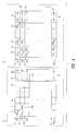
- a digital system 10which may be a computer (personal computer (PC)), digital camera, etc., is illustrated to include a host 12 , a controller device 14 and a flash memory unit 16 .
- the host 12includes a motherboard having a central processing unit (CPU), i.e., the “brain” of the digital system, coupled to access information through the controller device 14 from and to the memory unit 16 which, as depicted, is comprised of a flash memory device in accordance with the present invention.
- CPUcentral processing unit
- the controller device 14is an integrated circuit (or semiconductor) shown to include a host interface circuit 18 , a microprocessor 20 , a flash interface circuit 24 .
- the host interface 24is depicted to be coupled to the host 12 through host signals 28 , which includes an address bus, a bi-directional data bus and control signals (not shown separately).
- host signals 28which includes an address bus, a bi-directional data bus and control signals (not shown separately).
- the host address and data bussesmay be comprised of a single bus carrying both address and data information by multiplexing address and data signals onto the same bus. It should be noted that wherever the term bus is used herein, it refers to multiple electrical conductors or signal lines.
- the host bus 28may be a PCMCIA interface, an ATA interface or other kinds of interfaces employed by the industry.
- the host interface 18is shown coupled to the host bus 28 and is further shown to be coupled through a microprocessor bus 30 to the microprocessor 20 .
- Microprocessor 20is further coupled to the flash interface 24 through the microprocessor bus 30 , which facilitates communication of address and data information and control signals therebetween.
- the flash interface 24includes a space manager block 26 and optionally includes a tally register 22 .
- the flash interface circuit 24is coupled to the memory unit 16 through a flash address bus 34 , a bi-directional flash data bus 36 and flash control signals 38 .
- the tally register 22if employed, is used to temporarily store a tally value for use by the space manager 26 and the memory unit 16 , as will be explained shortly.
- the host 12may be required to access the memory unit 16 during performance of various operations such as reading and writing. In doing so, the host 12 provides the address of a block of information it wishes to access (commonly referred to as the logical block address (LBA)) to the controller 14 through the host bus 28 .
- LBAlogical block address
- a block of informationis typically a sector as employed in conventional hard disk drives, with each sector typically having 512 bytes of data, although other-sized sectors may be similarly employed.
- Microprocessor 20executes instructions in the form of program code from a memory structure (such as ROM (read-only memory) or RAM (read-and-write memory)) located within the microprocessor 20 block (but not shown) to instruct the space manager 26 to translate the LBA, provided by the host, to the next unused (or free) addressable storage block location available within the memory unit 16 .
- the translated addressis commonly referred to as a physical block address (PBA).
- PBAphysical block address
- the space managermay employ any one of a variety of algorithms to find the next available (or free) block located within the flash memory devices.
- An example of a space manageris disclosed in the earlier-referenced U.S. Pat. No. 5,485,595, the disclosure of which is herein incorporated by reference, particularly with reference to FIGS. 11-13, although other space management methods and apparatus may likewise be employed by the present invention.
- Memory unit 16generally includes a plurality of flash memory chips (or devices), labeled as 42 - 46 (in FIG. 1 ). These devices are non-volatile memory devices with characteristics as discussed above. FIG. 1 shows M number of flash chips, although for certain applications, a single flash chip may be alternatively employed.
- Each of the memory devices within the memory unit 16includes addressable locations 48 for storing information such as data files, and within each flash device 42 - 46 there may be a predefined storage area for storing LBA-PBA mapping data as schematically indicated at buffer 50 .
- Each one of the flash devicesshown in the preferred embodiment of FIG. 1, has a capacity of 4 Mbytes and is therefore capable of storing 8192 sectors with each sector being 512 bytes. Flash devices and blocks having alternative sizes may be similarly employed.
- buffer 50Within the buffer 50 is included a plurality of LBA rows, each row individually addressable by an LBA and having multiple PBA storage locations for storing PBA values that are assigned by the space manager. That is, buffer 50 is shown to include N LBA rows 58 - 64 .
- each LBA row of the buffer 50includes 16 PBA storage locations starting with PBA storage location 72 , 74 , to 78 .
- different numbers of PBA locationsmay be assigned to each LBA.
- the number of assigned PBA locations in an LBA rowmay affect the system performance. That is, the greater the number of PBA location per LBA, the less frequently erase operations may be required. Nevertheless, using more PBA locations per LBA row requires more flash memory space and leads to decreasing memory capacity within the digital system 10 .
- Each PBA location of the preferred embodiment shown in FIG. 1stores a 16-bit PBA value. This is also a design choice that may be readily different in other embodiments of the present invention.
- Each LBA rowfurther includes a tally storage location, which maintains the status of the latest (or most recent) PBA location for a corresponding LBA.
- Having 16 PBA locations assigned to each LBA row of a bufferrequires each tally storage location (within an LBA row) to be 2 bytes wide(or 16 bits with each byte being 8 bits) in order to allow a tally value stored in the tally storage location to point to any of the 16 PBA locations within a row.
- each tally storage locationmust have storage space for at least as many bits as there are PBA locations for a particular LBA because each bit in the tally storage location represents the status of each of the PBA values (within each of the PBA locations).
- the tally storage location for each LBA rowmay be located in other than non-volatile memory.
- a RAMnot shown
- other volatile memory deviceseither within the controller 14 or located externally to the controller may be used to store the tally values.
- a countermay be employed and incremented by one when a new PBA is written to an LBA row.
- the tally storage locationmay store less than the number of PBA locations within an LBA row. For example, where 16 PBA locations are included within an LBA row, the tally storage location may be 4 bits instead of 16 bits. Given 4 bits, the state of 16 PBAs may be represented just as well as using 16 bits.
- Thismay be employed in systems using a volatile memory location to store tally values due to their modifiable nature in that the tally value may be changed each time a new PBA is written. But when writing the tally values in nonvolatile memory such as in flash devices (as shown in FIG. 1 ), the tally value must maintain the same number of bits as the number of PBA locations within an LBA row because the tally value can not be modified or over-written prior to being first erased.
- FIG. 1shows the tally storage location 80 included in LBA row 60 , the tally storage location 88 included in LBA row 62 , the tally storage location 90 in LBA row 58 and so forth for each of the N LBA rows of buffer 50 .
- Each tally storage locationmaintains information regarding the location of the most recent (or current) PBA value corresponding to the LBA of the row in which the tally storage location is located. More specifically, the bits in a tally storage location effectively serve as a pointer to the most current PBA location within the LBA row where the tally storage location is located.
- the size of the LBA rows, the PBA locations, the tally storage locations and the number of PBA locations within an LBA rowmay be other than those discussed above with reference to the preferred embodiment.
- the flash devices 42 , 44 through 46 within the flash memory unit 16will be erased, and after the erase operation, all of the cells. within each flash device, 42 - 46 , will be set to logic state ‘1’. Therefore, all tally storage locations 70 , 80 , 88 , 100 , . . . will be set to an all ‘1's (or ‘111 . . . 111’ in binary or ‘FFFF’ in hexadecimal notation) state as seen in FIG. 1 . This indicates that no LBA has yet been accessed by the host or otherwise.
- the flash interface circuit 24will address the row within the flash device 42 wherein LBA 0 is located, e.g. LBA row 60 .
- the bits in the tally storage location 80will all be at logic state ‘1’ because the first time the digital system 10 is powered-up, the flash memory unit 16 is erased and all of the storage locations within the flash devices of the flash memory unit 16 will be at an erased state of ‘1’. This indicates that all of the PBA locations within LBA row 60 are available for storage. Therefore, the corresponding PBA, provided by space manager 26 , will be stored in the first PBA location 72 within LBA row 60 (starting from the left side of the LBA row 60 ).
- the first bit in the tally storage location 80 in LBA row 60will be set to logic state ‘0’ (in other words, the value in tally storage location 80 will be ‘111 . . . 110’ (in binary notation) or ‘FFFE’ (in hexadecimal notation) indicating that the most recent PBA value corresponding to LBA 0 is stored in PBA location 72 of LBA row 60 .
- the stored PBA valueis then used to locate a block within the flash memory unit 16 to retrieve information during a read operation.
- the value stored in tally storage location 80indicates the location of the most recent PBA value corresponding to the LBA being accessed by the host.
- the most recent PBA valueis used as the address of the location within the flash memory unit 16 to be read.
- the PBA valueremains the same while during a write operation, a new PBA value is written, as described above.
- the controller 14first transfers the most recent PBA values in each LBA row to a temporary storage location (such as a RAM (not shown) or to other flash memory data file locations 48 in flash device 44 or 46 ).
- the most recent PBA values in each LBA roware identified by using corresponding tally values for each row, i.e., the tally value of each LBA row points to the most recent PBA value for that row. For those LBA rows having all ones as their tally value, no PBA is transferred because none has yet been written.
- the memory cells defining buffer 50are erased (this erase operation may include erasure of the entire flash memory device 42 ).
- this erase operationmay include erasure of the entire flash memory device 42 .
- the most recent PBA valuesare written back into the buffer 50 . But they are not necessarily written to the same PBA locations from which they were transferred prior to the erase operation. In fact, they are written to the first corresponding PBA location of each of the LBA rows.
- the tally values of each LBA row for which a PBA value was writtenare set to ‘FFFE’ (in Hex. notation). Rows for which no PBA has been transferred, will have tally values of all ‘1's (or ‘FFFF’ in Hex.).
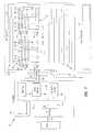
- the digital system 10is shown in FIG. 2 to employ another embodiment of the present invention wherein two buffers, buffers 50 and 52 , are used to store PBA-LBA mapping information in two different flash devices, 42 and 44 , respectively.
- a single flash devicemay store two LBA-PBA mappings (not shown), which will be further discussed later.
- each flash devicedoes not necessarily include one or any LBA-PBA mapping area. That is, portions of the same buffer may be stored in different flash devices.
- the size of the bufferis a function of the memory capacity associated with the flash devices as well as the number of LBAs and the number of PBAs per LBA.
- the flash interface 24is shown in FIG. 2 to further include an LBA buffer pointer block 40 coupled to the space manager 26 through the signal lines 32 .
- the LBA buffer pointeris also coupled through the microprocessor bus 30 to the microprocessor 20 .
- LBA row 60is shown as the first row in buffer 50 and LBA row 54 is shown as the first row of buffer 52 , both rows being assigned to and addressable by a common LBA, namely LBA 0 .
- LBA row 62 and LBA row 112of each buffer, 50 and 52 , respectively, is assigned to LBA 1 .
- Buffer 52generally stores the same kind of information as that stored in buffer 50 . Furthermore, the discussion above with reference to buffer 50 in FIG. 1 pertains to the buffer 52 in FIG. 2 . Additionally, the discussion above generally pertains to buffer 52 . That is, buffer 52 includes N LBA rows 54 , 56 , 66 and 112 . LBA row 54 is shown as the first row of buffer 52 . Both of the first rows, row 60 and 54 , in the buffers 50 and 52 are assigned to and addressable by a common LBA, namely LBA 0 . Similarly, the second row, LBA row 62 and LBA row 112 , of each buffer, 50 and 52 , respectively, is assigned to LBA 1 . Likewise, each LBA row in buffer 50 is identified by the same LBA row number as the corresponding LBA row in buffer 52 .
- LBA row 54includes PBA storage locations 82 , 84 , 86 and 94 .
- each of the N LBA rows within the buffer 52includes at least one (preferably more than one) PBA storage location.
- each LBA row of each bufferhas 16 PBA storage locations.
- LBA 0is assigned a total of 32 PBA storage locations, 16 PBA storage locations 72 , 74 , . . . 78 in buffer 50 and 16 PBA storage locations, 82 , 84 , . . . 94 , in buffer 54 .
- different numbers of PBA locationsmay be assigned to each LBA.
- FIG. 2shows the LBA row 54 of buffer 52 to include a tally storage location 100 , and LBA row 112 of buffer 52 to include tally storage location 102 and so forth with respect to each of the N LBA rows in that buffer.
- the flash memory unit 16is erased upon the first time the digital system 10 is powered-up in much the same way as discussed with respect to FIG. 1 .
- all of the cells within each flash device, 42 - 46will be set to logic state ‘1’. Therefore, all tally storage locations 70 , 80 , 88 , 100 , . . . will all be set to ‘111 . . . 111’ (or ‘FFFF’ in hexadecimal notation) as seen in FIG. 1 . This indicates that no LBA has yet been accessed by the host or otherwise.
- the PBAs corresponding to the appropriate LBA rowsare written into one of the buffers 50 or 52 , as earlier discussed.
- having two buffersallows PBAs to be further written into the second buffer after the first buffer is near to or completely full. This will be explained with respect to various examples.
- the second buffercan be used for further maintaining the LBA-PBA mapping information.
- the initial designation of the buffers as to which is primary and which is secondaryis an arbitrary design choice where buffer 52 may be chosen as the primary buffer and buffer 50 , the secondary buffer (for the purpose of discussion, buffer 50 will be initially designated as the primary buffer).
- the primary bufferis transferred to the secondary buffer and the first buffer is erased by microprocessor 20 for re-use. This concept will be better illustrated with reference to FIGS. 2-5.
- the LBA buffer pointer 40 in FIG. 2tracks the status of buffers 50 and 52 , as to indicating whether one or both buffers are in use and which one of the buffers is the primary and which is the secondary buffer. To so indicate, the LBA buffer pointer 40 maintains a 2-bit value regarding the state of buffers 50 and 52 as follows:
- Buffer 50is primary and buffer 52 is not used ‘01’ Buffer 50 is primary and buffer 52 is secondary ‘10’ Buffer 50 is not used and buffer 52 is primary ‘11’ buffer 50 is secondary and buffer 52 is primary
- LBA buffer pointer 40is not necessary and the information shown in Table 1 is maintained by microprocessor 20 in the form of firmware/software code.
- the value in LBA buffer pointer 40should be restored to the same value maintained therein when the system was last operational.
- the contents of LBA buffer pointer 40may be stored in flash memory unit 16 for preservation between power interruptions.
- the value in the LBA buffer pointer 40may not be preserved and upon power-up the microprocessor 20 may read the tally values in each of the buffers 50 and 52 to determine which buffer is the primary buffer and which is the secondary buffer.
- the latter bufferis not the secondary buffer.
- all other rows of the buffermust be searched for tally values being all ‘ones’ and if such a condition is met, then a determination is made that no secondary buffer is in use.
- the value of the LBA buffer pointer 40is preserved during power interruptions and it is read upon power-up to determine the state of the primary and the secondary buffers.
- the LBA buffer pointer 40may contain any value, although a reset signal of the kind generally applied in digital electronics systems may be applied to LBA buffer pointer 40 to ensure having a known value stored therein, such a value may be ‘00’.
- FIGS. 3-6illustrate examples of the states of buffers 50 and 52 in accordance with the state of the LBA buffer pointer 40 .
- FIG. 3is an example of what the states of buffers 50 and 52 may be when the LBA buffer pointer 40 contains the value ‘00’.
- FIG. 4is an example of what the states of buffers 50 and 52 may be when LBA buffer pointer 40 contains the value ‘01’.
- FIG. 5is an example of what the states of buffers 50 and 52 may be when LBA buffer pointer 40 contains the value ‘10’.
- FIG. 6is an example of what the states of buffers 50 and 52 may be when LBA buffer pointer 40 contains the value ‘11’.
- buffer 50will be designated as the primary buffer and buffer 52 will not be used. It should be obvious to those skilled in the art that the choice of designating a buffer as primary or secondary is initially random. That is, the primary buffer may be initially designated as buffer 52 and the secondary buffer may be buffer 50 without departing from the scope and spirit of the invention.
- LBA 0the first time it is accessed, its corresponding PBA value will be stored in PBA location 72 . Additionally, the value in tally storage location 80 will be modified from ‘FFFF’ (in hexadecimal notation) to ‘FFFE’. This new value in tally storage location 80 accordingly reflects the location of the most recent PBA value corresponding to LBA 0 , which is PBA location 72 .
- the LBA row 54 in the secondary buffer, buffer 52remains unchanged because pursuant to the contents of the LBA buffer pointer 40 , this buffer is not in use.
- LBA 1has been written at least twice with its most recently-assigned PBA being in PBA location 110 . That is, in accordance with the two-least significant bits of the value in tally storage location 88 , which are ‘0's, and the remaining bits being ‘ 1 's, the second PBA location in LBA row 62 is the most recent PBA value corresponding to LBA 1 .
- the LBA row 112 in the secondary buffer, buffer 52remains unchanged for the same reason given above with respect to LBA row 60 , i.e., the secondary buffer, buffer 52 , is not in use.
- LBA buffer pointer 40While the value in LBA buffer pointer 40 (in FIG. 2) is set to ‘00’, PBA entries are made in accordance with the description above until the contents of one of the tally storage locations, 80 , 88 , . . . , 90 - 92 , of the N LBA rows, is all ‘0's. Upon such an occurrence, during the next write operation of the same LBA row, based upon the tally value being all ‘0's, the space manager 26 will change the contents of the LBA buffer pointer 40 to logic state ‘01’. The state of the LBA buffer pointer 40 now indicates that the buffer 50 is the primary buffer and the buffer 52 is the secondary buffer and they are both in use.
- FIG. 4shows an example of buffers 50 and 52 when the contents of LBA buffer pointer 40 (in FIG. 2) is set to logic state ‘01’.
- measuresneed to be taken to avoid completely filling any or all of the LBA rows in both buffers. Otherwise, mapping information regarding the relationship between LBAs and PBAs stands to be lost rendering the system inoperative.
- Prevention of such a situationrequires the use of a criteria by which: 1) the mapping information from the primary buffer is transferred to the secondary buffer and 2) erasure of the flash memory chip incorporating the primary buffer is performed, where both the transfer and erase operations are completed prior to the complete usage of any of the rows within the secondary buffer.
- the criteria used in the preferred embodimentis as follows. Whenever the status register contents indicates that there are two buffers in use, that is, when the value in the LBA buffer pointer 40 is either ‘01’ or ‘11’, during the next write of an LBA row within the primary buffer, all of the bits of the corresponding tally storage location in the LBA row being accessed are set to logic state ‘0’ and the corresponding PBA value is actually stored in the secondary rather than the primary buffer. Accordingly, the tally value of the corresponding LBA row of the secondary buffer is modified to logic state “FFFE”. This operation however, is not necessary to perform for LBA rows whose tally value is all ‘0's. In this respect, as each of the LBA rows is accessed, the information in the primary buffer is transferred to the secondary buffer.
- LBA Nwhich is the most current PBA value in LBA row 64 is transferred to the first PBA location of LBA row 66 in buffer 52 .
- the value in tally storage location 70 in that rowis set to ‘FFFE’ and the value in tally storage location 92 , in LBA row 64 , is set to all ‘0's (not shown in FIG. 4 ).
- the secondary bufferis updated with a new PBA entry.
- the new PBA valuewill be placed in PBA location 82 of LBA row 54 in buffer 52 .
- the value in tally storage location 100will be set to ‘FFFE’ and the value in tally storage location 80 will be set to all ‘0's (not shown).
- PBA location 82will now include the most recent PBA value assigned to LBA 0 .
- the preferred embodimentavoids transfer of LBA row information from the primary buffer to the secondary buffer since they have already been moved to the secondary buffer. Likewise, for those LBA rows having values of all ‘1's in their corresponding tally locations, the preferred embodiment does not transfer any LBA row information from one buffer to another buffer. This is due to the lack of any valid PBA entries in such rows.
- any additional PBA entries for all rowswill be stored in the secondary buffer.
- the values in tally storage locations of the secondary buffer, rather than the primary buffer,will be updated to indicate the position of the most recent PBA entry.
- the value of tally storage location 88has been set to logic state ‘0’, the PBA values corresponding to LBA 1 will be stored in the PBA location of LBA row 112 of buffer 52 .
- the most recent PBA locationis shown to be PBA location 118 as evidenced by the value in tally storage location 102 being ‘FFF’ (in hexadecimal notation).
- FIG. 5shows an example of what the contents of buffer 50 and 52 may be when LBA buffer pointer 40 is set to ‘10’. As stated in Table 1, only one buffer is in use in this state and that is buffer 52 if we were to follow the example provided thus far. In fact, the primary buffer is now buffer 52 and the secondary buffer is now buffer 50 , which is not used.
- PBA valuesare directly placed in PBA locations of LBA rows within the primary buffer 52 in the same manner as discussed earlier with respect to buffer 50 .
- LBA row 54includes one PBA entry in PBA location 82 and tally location 100 indicates that this is the most recent PBA entry because the value in tally location 100 is ‘FFFE’.
- buffer 50During an erase command, initiated by the microprocessor 20 , the contents of buffer 50 will be erased thereby placing the states of all of the storage locations within buffer 50 (such as PBA locations, tally storage locations and the like) at a predetermined erased state, which is generally logic state ‘1’.
- the primary buffercontinues to be in-use until one of its LBA rows is full (or near full) as discussed earlier. Upon such an occurrence, the state of LBA buffer pointer 40 (in FIG. 2) will be changed to ‘11’, indicating that buffer 52 will be the primary buffer and buffer 50 will be used as the secondary buffer, as stated in Table 1.
- FIG. 6shows an example of what the buffers 50 and 52 may include when the state of LBA buffer pointer 40 is at logic state ‘11’.
- LBA rows 54 and 112 of primary buffer 52have been completely utilized.
- secondary buffer 50includes the most-recently assigned PBA value corresponding to LBA in PBA location 72 , as directed-to by the value in tally storage location 80 .
- the value in tally storage location 88 ‘FFFC’shows the most current corresponding PBA, PBA to LBAl to be in PBA location 110 , and so on.
- the contents of the primary bufferis ultimately transferred to the secondary buffer for each LBA row except those rows which either have not been used (as indicated by their tally values being all ‘1's) or have been entirely used, as indicated by their tally value being all ‘0’'s. This process is the same as that discussed with reference to FIG. 4 where both buffers were in-use.
- the microprocessorwill move the remaining valid PBAs (valid PBAs are those PBAs for which corresponding tally value for the same row is not either ‘FFFF’ or ‘0000’) from the primary buffer to the secondary buffer.
- the microprocessordoes not have to wait for one of the PBA entries in the secondary buffer to reach the “close to full” state to initiate moving the remaining valid PBAs from the primary to the secondary buffer.
- the microprocessormay initiate the move as soon as one of the entries in the primary buffer is full. It could then move the particular LBA, along with all of the other valid PBAs belonging to other LBAs and set to the status of the LBA buffer pointer to point to the secondary buffer being the primary buffer with no secondary buffer in use.
- the preferred embodiment of the present inventioncontinuously switches storage of PBA-LBA information between the buffers 50 and 52 .
- Swapping between a primary and a secondary buffer (or table) in the manner described hereinmay be referred to as creating a “ping-pong” effect between the two buffers whereby buffer 50 is the “ping” when it is designated as the primary buffer the “pong” the rest of the time during which it is designated as the “pong.”
- buffer 52is the same applies to buffer 52 .
- Each bufferwould similarly include LBA rows where each LBA would have associated therewith, LBA rows of like location within each buffer, such as for example LBA rows 60 and 54 in association with LBA 0 . It should be further apparent to those skilled in the art that addition of buffers increases the storage space required therefore in the flash memory devices. Moreover, more than two bits of status will be required for indicating the buffer designations where additional buffers are employed.
- buffers 50 and 54may be stored in the same flash memory device 42 and the remaining flash memory devices may not include any buffers therein.
- the host 12still reads/writes blocks of data in 48 of flash memory devices 42 , 44 , 46 and the like, such as previously discussed.
- the LBA-PBA mapping informationhowever, is stored in flash memory device 42 , specifically within buffers 50 and 52 , in the same manner as described with reference to FIGS. 3-6.
- the flash memory unit 16may be configured to store buffers such as 50 and 52 within any flash memory device.
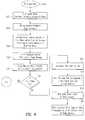
- FIGS. 8 and 9, respectively,provide flow charts of read and write operations to and from the flash memory devices using the methods and apparatus of the above-discussed embodiments of the present invention.
- a read operationis initiated by the host.
- the hostsends a read command at step 1002 which includes an LBA address of the block it desires to read.
- the microprocessor 20interprets the read command at step 1004 and issues a read sector command to the space manager 26 at step 1006 .
- the space managerreads the tally value stored in an LBA row corresponding to the LBA sent by the host.
- the space managerreads the most recent PBA value at step 1014 .
- a block of informationis then read from a location in the flash memory devices identified by the read PBA value at step 1016 . Note that at step 1012 , if the tally value is not valid, an error condition is returned to the host.
- an example of a write operationis shown in flow chart form to include step 1020 at which time a write operation is initiated by the host.
- the hostsends a write command at step 1022 .
- the hostprovides address and data corresponding to the block of information being written to the controller 14 .
- the microprocessorinterprets the write command and initiates a search for a free or available block of memory space within the flash memory devices (at step 1026 ) by sending a command to the space manager to do the same.
- the space managerlocates a free block within the flash memory devices at 1028 and at step 1030 reads the tally value, which would have been retrieved from the flash memory if stored there or from a volatile area of memory as discussed previously. If the tally value is determined to be valid at 1032 (i.e. it is not all ones), it is either incremented by one when it is kept in other than non-volatile (or flash memory) or if it is stored in flash memory, the bit of the tally value corresponding to the position of the most recent PBA value in the LBA row being addressed is modified from ‘1’ to ‘0’.
- the new PBA (found by the space manager) valueis written in the appropriate LBA row at step 1036 and at step 1038 , data is written to the area in the flash memory devices identified by the new PBA.
- the extension portion of the sector(such as ECC, flags and LBA) is written to the flash memory device.
Landscapes
- Engineering & Computer Science (AREA)
- Theoretical Computer Science (AREA)
- Physics & Mathematics (AREA)
- General Engineering & Computer Science (AREA)
- General Physics & Mathematics (AREA)
- Human Computer Interaction (AREA)
- Techniques For Improving Reliability Of Storages (AREA)
- Read Only Memory (AREA)
Abstract
Description
| TABLE 1 | |
| STATUS REGISTER CONTENTS | STATUS OF BUFFERS |
| ‘00’ | |
| ‘01’ | |
| ‘10’ | |
| ‘11’ | |
Claims (22)
Priority Applications (1)
| Application Number | Priority Date | Filing Date | Title |
|---|---|---|---|
| US09/580,392US6327639B1 (en) | 1997-12-11 | 2000-05-26 | Method and apparatus for storing location identification information within non-volatile memory devices |
Applications Claiming Priority (2)
| Application Number | Priority Date | Filing Date | Title |
|---|---|---|---|
| US08/988,844US6076137A (en) | 1997-12-11 | 1997-12-11 | Method and apparatus for storing location identification information within non-volatile memory devices |
| US09/580,392US6327639B1 (en) | 1997-12-11 | 2000-05-26 | Method and apparatus for storing location identification information within non-volatile memory devices |
Related Parent Applications (1)
| Application Number | Title | Priority Date | Filing Date |
|---|---|---|---|
| US08/988,844ContinuationUS6076137A (en) | 1997-12-11 | 1997-12-11 | Method and apparatus for storing location identification information within non-volatile memory devices |
Publications (1)
| Publication Number | Publication Date |
|---|---|
| US6327639B1true US6327639B1 (en) | 2001-12-04 |
Family
ID=25534531
Family Applications (2)
| Application Number | Title | Priority Date | Filing Date |
|---|---|---|---|
| US08/988,844Expired - LifetimeUS6076137A (en) | 1997-12-11 | 1997-12-11 | Method and apparatus for storing location identification information within non-volatile memory devices |
| US09/580,392Expired - LifetimeUS6327639B1 (en) | 1997-12-11 | 2000-05-26 | Method and apparatus for storing location identification information within non-volatile memory devices |
Family Applications Before (1)
| Application Number | Title | Priority Date | Filing Date |
|---|---|---|---|
| US08/988,844Expired - LifetimeUS6076137A (en) | 1997-12-11 | 1997-12-11 | Method and apparatus for storing location identification information within non-volatile memory devices |
Country Status (1)
| Country | Link |
|---|---|
| US (2) | US6076137A (en) |
Cited By (49)
| Publication number | Priority date | Publication date | Assignee | Title |
|---|---|---|---|---|
| US6421276B1 (en)* | 2001-08-09 | 2002-07-16 | Tower Semiconductor Ltd. | Method and apparatus for controlling erase operations of a non-volatile memory system |
| US20020184436A1 (en)* | 2001-06-04 | 2002-12-05 | Samsung Electronics Co., Ltd. | Flash memory management method |
| US20030024993A1 (en)* | 2001-07-27 | 2003-02-06 | Colin Gould | Memory management method and smartcard employing same |
| US6549442B1 (en) | 2002-07-25 | 2003-04-15 | Neomagic Corp. | Hardware-assisted fast bank-swap in a content-addressable-memory (CAM) processor |
| US20030091036A1 (en)* | 2001-10-04 | 2003-05-15 | Milliken Walter Clark | Execution unit for a network processor |
| WO2003094509A1 (en)* | 2002-04-29 | 2003-11-13 | Thomson Licensing Inc. | Pre-power-failure storage of television parameters in nonvolatile memory |
| US20040057316A1 (en)* | 2002-09-25 | 2004-03-25 | Renesas Technology Corp. | Nonvolatile memory |
| US6721819B2 (en) | 1998-03-02 | 2004-04-13 | Lexar Media, Inc. | Flash memory card with enhanced operating mode detection and user-friendly interfacing system |
| US6772274B1 (en) | 2000-09-13 | 2004-08-03 | Lexar Media, Inc. | Flash memory system and method implementing LBA to PBA correlation within flash memory array |
| US20050021904A1 (en)* | 2003-06-05 | 2005-01-27 | Stmicroelectronics S.R.L. | Mass memory device based on a flash memory with multiple buffers |
| US6901457B1 (en) | 1998-11-04 | 2005-05-31 | Sandisk Corporation | Multiple mode communications system |
| US20050281105A1 (en)* | 2004-06-22 | 2005-12-22 | Takashi Oshima | Memory card, semiconductor device, and method of controlling semiconductor memory |
| US20060022054A1 (en)* | 2004-07-28 | 2006-02-02 | Reuven Elhamias | Optimized non-volatile storage systems |
| US20060136657A1 (en)* | 2004-12-22 | 2006-06-22 | Intel Corporation | Embedding a filesystem into a non-volatile device |
| US20060184721A1 (en)* | 2005-02-16 | 2006-08-17 | Chen Ben W | Configurable flash memory controller and method of use |
| US7102671B1 (en) | 2000-02-08 | 2006-09-05 | Lexar Media, Inc. | Enhanced compact flash memory card |
| US7155559B1 (en) | 2000-08-25 | 2006-12-26 | Lexar Media, Inc. | Flash memory architecture with separate storage of overhead and user data |
| US7167944B1 (en) | 2000-07-21 | 2007-01-23 | Lexar Media, Inc. | Block management for mass storage |
| US7185208B2 (en) | 2001-09-28 | 2007-02-27 | Lexar Media, Inc. | Data processing |
| US7215580B2 (en) | 2001-09-28 | 2007-05-08 | Lexar Media, Inc. | Non-volatile memory control |
| US7231643B1 (en) | 2002-02-22 | 2007-06-12 | Lexar Media, Inc. | Image rescue system including direct communication between an application program and a device driver |
| US7254724B2 (en) | 2001-09-28 | 2007-08-07 | Lexar Media, Inc. | Power management system |
| US7263591B2 (en) | 1995-07-31 | 2007-08-28 | Lexar Media, Inc. | Increasing the memory performance of flash memory devices by writing sectors simultaneously to multiple flash memory devices |
| US7277011B2 (en) | 2002-02-22 | 2007-10-02 | Micron Technology, Inc. | Removable memory media with integral indicator light |
| US7275686B2 (en) | 2003-12-17 | 2007-10-02 | Lexar Media, Inc. | Electronic equipment point-of-sale activation to avoid theft |
| US20080031050A1 (en)* | 2006-08-03 | 2008-02-07 | Samsung Electronics Co., Ltd. | Flash memory device having a data buffer and programming method of the same |
| US7340581B2 (en) | 2001-09-28 | 2008-03-04 | Lexar Media, Inc. | Method of writing data to non-volatile memory |
| US7370166B1 (en) | 2004-04-30 | 2008-05-06 | Lexar Media, Inc. | Secure portable storage device |
| US20080162789A1 (en)* | 2007-01-03 | 2008-07-03 | Choi Jin-Hyeok | Memory system with backup circuit and programming method |
| US7441090B2 (en) | 1995-07-31 | 2008-10-21 | Lexar Media, Inc. | System and method for updating data sectors in a non-volatile memory using logical block addressing |
| US7464306B1 (en) | 2004-08-27 | 2008-12-09 | Lexar Media, Inc. | Status of overall health of nonvolatile memory |
| US7523249B1 (en) | 1995-07-31 | 2009-04-21 | Lexar Media, Inc. | Direct logical block addressing flash memory mass storage architecture |
| US7543077B1 (en) | 2000-09-19 | 2009-06-02 | Stragent, Llc | Ternary content addressable memory embedded in a central processing unit |
| US7594063B1 (en) | 2004-08-27 | 2009-09-22 | Lexar Media, Inc. | Storage capacity status |
| US7634624B2 (en) | 2001-09-28 | 2009-12-15 | Micron Technology, Inc. | Memory system for data storage and retrieval |
| US20100067298A1 (en)* | 2000-02-17 | 2010-03-18 | Conley Kevin M | Flash EEprom System With Simultaneous Multiple Data Sector Programming and Storage of Physical Block Characteristics in Other Designated Blocks |
| US7725628B1 (en) | 2004-04-20 | 2010-05-25 | Lexar Media, Inc. | Direct secondary device interface by a host |
| US20100228940A1 (en)* | 2009-03-04 | 2010-09-09 | Micron Technology, Inc. | Memory block management |
| US20100228928A1 (en)* | 2009-03-04 | 2010-09-09 | Micron Technology, Inc. | Memory block selection |
| US20100262721A1 (en)* | 2009-04-09 | 2010-10-14 | Micron Technology, Inc. | Memory controllers, memory systems, solid state drives and methods for processing a number of commands |
| US8078848B2 (en) | 2009-01-09 | 2011-12-13 | Micron Technology, Inc. | Memory controller having front end and back end channels for modifying commands |
| US8171203B2 (en) | 1995-07-31 | 2012-05-01 | Micron Technology, Inc. | Faster write operations to nonvolatile memory using FSInfo sector manipulation |
| US8276042B2 (en) | 2009-02-03 | 2012-09-25 | Micron Technology, Inc. | Determining sector status in a memory device |
| US8335224B1 (en)* | 2001-10-12 | 2012-12-18 | Raytheon Bbn Technologies Corp. | Data-buffering apparatus and method |
| US20130305009A1 (en)* | 2012-05-09 | 2013-11-14 | Luke Durant | Virtual memory structure for coprocessors having memory allocation limitations |
| US20150052291A1 (en)* | 2013-08-19 | 2015-02-19 | Fujitsu Limited | Semiconductor storage device and semiconductor storage device control method |
| US9411721B2 (en) | 2013-11-15 | 2016-08-09 | Sandisk Technologies Llc | Detecting access sequences for data compression on non-volatile memory devices |
| US10365841B2 (en) | 2011-12-12 | 2019-07-30 | Sandisk Technologies Llc | Non-volatile storage systems with go to sleep adaption |
| US11615019B2 (en) | 2018-08-21 | 2023-03-28 | Sony Corporation | Non-volatile storage device, host device, and data storage system to increase data write speed |
Families Citing this family (55)
| Publication number | Priority date | Publication date | Assignee | Title |
|---|---|---|---|---|
| US6076137A (en)* | 1997-12-11 | 2000-06-13 | Lexar Media, Inc. | Method and apparatus for storing location identification information within non-volatile memory devices |
| US6226728B1 (en)* | 1998-04-21 | 2001-05-01 | Intel Corporation | Dynamic allocation for efficient management of variable sized data within a nonvolatile memory |
| US6195732B1 (en)* | 1999-01-22 | 2001-02-27 | Quantum Corp. | Storage device capacity management |
| US6393514B1 (en)* | 1999-07-12 | 2002-05-21 | Netlogic Microsystems, Inc. | Method of generating an almost full flag and a full flag in a content addressable memory |
| US6721843B1 (en) | 2000-07-07 | 2004-04-13 | Lexar Media, Inc. | Flash memory architecture implementing simultaneously programmable multiple flash memory banks that are host compatible |
| US7113432B2 (en) | 2000-09-14 | 2006-09-26 | Sandisk Corporation | Compressed event counting technique and application to a flash memory system |
| US7404021B2 (en)* | 2000-11-17 | 2008-07-22 | Aristos Logic Corporation | Integrated input/output controller |
| US7155560B2 (en)* | 2001-06-27 | 2006-12-26 | Intel Corporation | Method and apparatus for storing data in flash memory |
| US6977847B2 (en)* | 2001-11-23 | 2005-12-20 | M-Systems Flash Disk Pioneers Ltd. | Detecting partially erased units in flash devices |
| US7606364B1 (en) | 2002-04-23 | 2009-10-20 | Seagate Technology Llc | Disk drive with flexible data stream encryption |
| US6798353B2 (en) | 2002-04-24 | 2004-09-28 | Itron Electricity Metering, Inc. | Method of using flash memory for storing metering data |
| US20050036387A1 (en)* | 2002-04-24 | 2005-02-17 | Seal Brian K. | Method of using flash memory for storing metering data |
| EP1548602B1 (en)* | 2002-10-02 | 2008-03-12 | Matsushita Electric Industrial Co., Ltd. | Non-volatile storage device control method |
| US6944063B2 (en)* | 2003-01-28 | 2005-09-13 | Sandisk Corporation | Non-volatile semiconductor memory with large erase blocks storing cycle counts |
| JP2005190288A (en)* | 2003-12-26 | 2005-07-14 | Tdk Corp | Memory controller, flash memory system therewith, and method for controlling flash memory |
| KR100533683B1 (en)* | 2004-02-03 | 2005-12-05 | 삼성전자주식회사 | Data managing device and method for flash memory |
| JP4153535B2 (en)* | 2006-05-30 | 2008-09-24 | Tdk株式会社 | MEMORY CONTROLLER, FLASH MEMORY SYSTEM PROVIDED WITH MEMORY CONTROLLER, AND FLASH MEMORY CONTROL METHOD |
| TWI326028B (en) | 2006-11-20 | 2010-06-11 | Silicon Motion Inc | Method for flash memory data management |
| US8959307B1 (en) | 2007-11-16 | 2015-02-17 | Bitmicro Networks, Inc. | Reduced latency memory read transactions in storage devices |
| US20100174845A1 (en)* | 2009-01-05 | 2010-07-08 | Sergey Anatolievich Gorobets | Wear Leveling for Non-Volatile Memories: Maintenance of Experience Count and Passive Techniques |
| US8700840B2 (en)* | 2009-01-05 | 2014-04-15 | SanDisk Technologies, Inc. | Nonvolatile memory with write cache having flush/eviction methods |
| US8094500B2 (en)* | 2009-01-05 | 2012-01-10 | Sandisk Technologies Inc. | Non-volatile memory and method with write cache partitioning |
| US8040744B2 (en)* | 2009-01-05 | 2011-10-18 | Sandisk Technologies Inc. | Spare block management of non-volatile memories |
| US8244960B2 (en)* | 2009-01-05 | 2012-08-14 | Sandisk Technologies Inc. | Non-volatile memory and method with write cache partition management methods |
| EP2234010A1 (en)* | 2009-03-23 | 2010-09-29 | Digi-Link Electronics Corporation | Method setting hidden storage area in a flash memory |
| US8665601B1 (en) | 2009-09-04 | 2014-03-04 | Bitmicro Networks, Inc. | Solid state drive with improved enclosure assembly |
| US8447908B2 (en) | 2009-09-07 | 2013-05-21 | Bitmicro Networks, Inc. | Multilevel memory bus system for solid-state mass storage |
| CN102023811B (en)* | 2009-09-10 | 2012-11-28 | 群联电子股份有限公司 | Method and system for issuing programmatic instructions to flash memory |
| US8560804B2 (en)* | 2009-09-14 | 2013-10-15 | Bitmicro Networks, Inc. | Reducing erase cycles in an electronic storage device that uses at least one erase-limited memory device |
| US9372755B1 (en)* | 2011-10-05 | 2016-06-21 | Bitmicro Networks, Inc. | Adaptive power cycle sequences for data recovery |
| US9152568B1 (en)* | 2011-12-05 | 2015-10-06 | Seagate Technology Llc | Environmental-based device operation |
| US9043669B1 (en) | 2012-05-18 | 2015-05-26 | Bitmicro Networks, Inc. | Distributed ECC engine for storage media |
| US8750043B2 (en)* | 2012-08-16 | 2014-06-10 | Winbond Electronics Corp. | Data storage device and control method for non-volatile memory |
| US9423457B2 (en) | 2013-03-14 | 2016-08-23 | Bitmicro Networks, Inc. | Self-test solution for delay locked loops |
| US9734067B1 (en) | 2013-03-15 | 2017-08-15 | Bitmicro Networks, Inc. | Write buffering |
| US9430386B2 (en) | 2013-03-15 | 2016-08-30 | Bitmicro Networks, Inc. | Multi-leveled cache management in a hybrid storage system |
| US9916213B1 (en) | 2013-03-15 | 2018-03-13 | Bitmicro Networks, Inc. | Bus arbitration with routing and failover mechanism |
| US9798688B1 (en) | 2013-03-15 | 2017-10-24 | Bitmicro Networks, Inc. | Bus arbitration with routing and failover mechanism |
| US9971524B1 (en) | 2013-03-15 | 2018-05-15 | Bitmicro Networks, Inc. | Scatter-gather approach for parallel data transfer in a mass storage system |
| US9842024B1 (en) | 2013-03-15 | 2017-12-12 | Bitmicro Networks, Inc. | Flash electronic disk with RAID controller |
| US9875205B1 (en) | 2013-03-15 | 2018-01-23 | Bitmicro Networks, Inc. | Network of memory systems |
| US9858084B2 (en) | 2013-03-15 | 2018-01-02 | Bitmicro Networks, Inc. | Copying of power-on reset sequencer descriptor from nonvolatile memory to random access memory |
| US9400617B2 (en) | 2013-03-15 | 2016-07-26 | Bitmicro Networks, Inc. | Hardware-assisted DMA transfer with dependency table configured to permit-in parallel-data drain from cache without processor intervention when filled or drained |
| US10489318B1 (en) | 2013-03-15 | 2019-11-26 | Bitmicro Networks, Inc. | Scatter-gather approach for parallel data transfer in a mass storage system |
| US9720603B1 (en) | 2013-03-15 | 2017-08-01 | Bitmicro Networks, Inc. | IOC to IOC distributed caching architecture |
| US9501436B1 (en) | 2013-03-15 | 2016-11-22 | Bitmicro Networks, Inc. | Multi-level message passing descriptor |
| US9672178B1 (en) | 2013-03-15 | 2017-06-06 | Bitmicro Networks, Inc. | Bit-mapped DMA transfer with dependency table configured to monitor status so that a processor is not rendered as a bottleneck in a system |
| US20150293705A1 (en)* | 2014-04-11 | 2015-10-15 | Seagate Technology Llc | Formatting and capacity expansion in a data storage device |
| US10055150B1 (en) | 2014-04-17 | 2018-08-21 | Bitmicro Networks, Inc. | Writing volatile scattered memory metadata to flash device |
| US10078604B1 (en) | 2014-04-17 | 2018-09-18 | Bitmicro Networks, Inc. | Interrupt coalescing |
| US9811461B1 (en) | 2014-04-17 | 2017-11-07 | Bitmicro Networks, Inc. | Data storage system |
| US10025736B1 (en) | 2014-04-17 | 2018-07-17 | Bitmicro Networks, Inc. | Exchange message protocol message transmission between two devices |
| US9952991B1 (en) | 2014-04-17 | 2018-04-24 | Bitmicro Networks, Inc. | Systematic method on queuing of descriptors for multiple flash intelligent DMA engine operation |
| US10042792B1 (en) | 2014-04-17 | 2018-08-07 | Bitmicro Networks, Inc. | Method for transferring and receiving frames across PCI express bus for SSD device |
| US10552050B1 (en) | 2017-04-07 | 2020-02-04 | Bitmicro Llc | Multi-dimensional computer storage system |
Citations (53)
| Publication number | Priority date | Publication date | Assignee | Title |
|---|---|---|---|---|
| US3633175A (en) | 1969-05-15 | 1972-01-04 | Honeywell Inc | Defect-tolerant digital memory system |
| US4405952A (en) | 1978-05-26 | 1983-09-20 | Cii Honeywell Bull | Apparatus for detecting faulty sectors and for allocating replacement sectors in a magnetic disc memory |
| JPS58215794A (en) | 1982-06-08 | 1983-12-15 | Toshiba Corp | Non-volatile memory device |
| JPS58215795A (en) | 1982-06-08 | 1983-12-15 | Toshiba Corp | Non-volatile memory device |
| WO1984000628A1 (en) | 1982-07-30 | 1984-02-16 | Western Electric Co | Management of defects in storage media |
| JPS5945695A (en) | 1982-09-07 | 1984-03-14 | Fujitsu Ltd | Ic memory |
| US4450599A (en) | 1981-04-30 | 1984-05-29 | Wurttembergische Parfumerie-Fabrik Gmbh | Electric toothbrush |
| US4456971A (en) | 1981-02-09 | 1984-06-26 | Sony Corporation | Semiconductor RAM that is accessible in magnetic disc storage format |
| JPS59162695A (en) | 1983-03-07 | 1984-09-13 | Nec Corp | Storage device |
| US4525839A (en) | 1981-10-30 | 1985-06-25 | Hitachi, Ltd. | Method of controlling storage device |
| JPS60212900A (en) | 1984-04-09 | 1985-10-25 | Nec Corp | Semiconductor fixed memory |
| JPS6196598A (en) | 1984-10-17 | 1986-05-15 | Fuji Electric Co Ltd | Electrically erasable P-ROM count data storage method |
| US4616311A (en) | 1980-10-03 | 1986-10-07 | Tokyo Shibaura Denki Kabushiki Kaisha | Data processing system |
| AU557723B2 (en) | 1982-12-17 | 1987-01-08 | Blue Circle Southern Cement Ltd. | Electronic memory system |
| US4654847A (en) | 1984-12-28 | 1987-03-31 | International Business Machines | Apparatus for automatically correcting erroneous data and for storing the corrected data in a common pool alternate memory array |
| EP0220718A2 (en) | 1985-10-29 | 1987-05-06 | Toppan Printing Co., Ltd. | IC card |
| EP0243503A1 (en) | 1985-10-28 | 1987-11-04 | Matsushita Electric Industrial Co., Ltd. | Data recording/regenerating device |
| US4710871A (en) | 1982-11-01 | 1987-12-01 | Ncr Corporation | Data transmitting and receiving apparatus |
| JPS62283497A (en) | 1986-05-31 | 1987-12-09 | Canon Inc | Memory write control method |
| JPS62283496A (en) | 1986-05-31 | 1987-12-09 | Canon Inc | Programmable read-only memory write count management method |
| US4746998A (en) | 1985-11-20 | 1988-05-24 | Seagate Technology, Inc. | Method for mapping around defective sectors in a disc drive |
| US4757474A (en) | 1986-01-28 | 1988-07-12 | Fujitsu Limited | Semiconductor memory device having redundancy circuit portion |
| JPS63183700A (en) | 1987-01-26 | 1988-07-29 | Mitsubishi Electric Corp | EEPROM access method |
| US4774700A (en) | 1985-03-12 | 1988-09-27 | Matsushita Electric Industrial Co., Ltd. | Information recording and reproducing apparatus with detection and management of defective sectors |
| US4800520A (en) | 1985-10-29 | 1989-01-24 | Kabushiki Kaisha Toshiba | Portable electronic device with garbage collection function |
| US4896262A (en) | 1984-02-24 | 1990-01-23 | Kabushiki Kaisha Meidensha | Emulation device for converting magnetic disc memory mode signal from computer into semiconductor memory access mode signal for semiconductor memory |
| US4914529A (en) | 1988-07-18 | 1990-04-03 | Western Digital Corp. | Data disk defect handling using relocation ID fields |
| US4920518A (en) | 1985-04-23 | 1990-04-24 | Hitachi, Ltd. | Semiconductor integrated circuit with nonvolatile memory |
| US4924331A (en) | 1985-11-20 | 1990-05-08 | Seagate Technology, Inc. | Method for mapping around defective sectors in a disc drive |
| US4953122A (en) | 1986-10-31 | 1990-08-28 | Laserdrive Ltd. | Pseudo-erasable and rewritable write-once optical disk memory system |
| EP0424191A2 (en) | 1989-10-17 | 1991-04-24 | Sundisk Corporation | Device and method for defect handling in semi-conductor memory |
| US5070474A (en) | 1988-07-26 | 1991-12-03 | Disk Emulation Systems, Inc. | Disk emulation system |
| EP0489204A1 (en) | 1990-12-04 | 1992-06-10 | Hewlett-Packard Limited | Reprogrammable data storage device |
| JPH04332999A (en) | 1991-05-07 | 1992-11-19 | Hitachi Koki Co Ltd | Method of using memory |
| EP0522780A2 (en) | 1991-07-12 | 1993-01-13 | International Business Machines Corporation | Control method for a computer memory device |
| EP0544252A2 (en) | 1991-11-28 | 1993-06-02 | Fujitsu Limited | Data management system for programming-limited type semiconductor memory and IC memory card having the data management system |
| US5226168A (en) | 1989-04-25 | 1993-07-06 | Seiko Epson Corporation | Semiconductor memory configured to emulate floppy and hard disk magnetic storage based upon a determined storage capacity of the semiconductor memory |
| FR2687811A1 (en) | 1992-02-20 | 1993-08-27 | Fujitsu Ltd | FLASH MEMORY CONTROL METHOD AND APPARATUS. |
| US5270979A (en) | 1991-03-15 | 1993-12-14 | Sundisk Corporation | Method for optimum erasing of EEPROM |
| US5297148A (en) | 1989-04-13 | 1994-03-22 | Sundisk Corporation | Flash eeprom system |
| US5303198A (en) | 1990-09-28 | 1994-04-12 | Fuji Photo Film Co., Ltd. | Method of recording data in memory card having EEPROM and memory card system using the same |
| US5337275A (en) | 1992-10-30 | 1994-08-09 | Intel Corporation | Method for releasing space in flash EEPROM memory array to allow the storage of compressed data |
| US5341330A (en) | 1992-10-30 | 1994-08-23 | Intel Corporation | Method for writing to a flash memory array during erase suspend intervals |
| US5341339A (en) | 1992-10-30 | 1994-08-23 | Intel Corporation | Method for wear leveling in a flash EEPROM memory |
| US5353256A (en) | 1993-06-30 | 1994-10-04 | Intel Corporation | Block specific status information in a memory device |
| US5357475A (en) | 1992-10-30 | 1994-10-18 | Intel Corporation | Method for detaching sectors in a flash EEPROM memory array |
| US5388083A (en) | 1993-03-26 | 1995-02-07 | Cirrus Logic, Inc. | Flash memory mass storage architecture |
| US5430859A (en) | 1991-07-26 | 1995-07-04 | Sundisk Corporation | Solid state memory system including plural memory chips and a serialized bus |
| US5479638A (en) | 1993-03-26 | 1995-12-26 | Cirrus Logic, Inc. | Flash memory mass storage architecture incorporation wear leveling technique |
| US5485595A (en) | 1993-03-26 | 1996-01-16 | Cirrus Logic, Inc. | Flash memory mass storage architecture incorporating wear leveling technique without using cam cells |
| US5544356A (en) | 1990-12-31 | 1996-08-06 | Intel Corporation | Block-erasable non-volatile semiconductor memory which tracks and stores the total number of write/erase cycles for each block |
| US5566314A (en) | 1993-08-30 | 1996-10-15 | Lucent Technologies Inc. | Flash memory device employing unused cell arrays to update files |
| US6076137A (en)* | 1997-12-11 | 2000-06-13 | Lexar Media, Inc. | Method and apparatus for storing location identification information within non-volatile memory devices |
Family Cites Families (3)
| Publication number | Priority date | Publication date | Assignee | Title |
|---|---|---|---|---|
| US4450559A (en)* | 1981-12-24 | 1984-05-22 | International Business Machines Corporation | Memory system with selective assignment of spare locations |
| US5860157A (en)* | 1994-01-26 | 1999-01-12 | Intel Corporation | Nonvolatile memory card controller with an optimized memory address mapping window scheme |
| US5835935A (en)* | 1995-09-13 | 1998-11-10 | Lexar Media, Inc. | Method of and architecture for controlling system data with automatic wear leveling in a semiconductor non-volatile mass storage memory |
- 1997
- 1997-12-11USUS08/988,844patent/US6076137A/ennot_activeExpired - Lifetime
- 2000
- 2000-05-26USUS09/580,392patent/US6327639B1/ennot_activeExpired - Lifetime
Patent Citations (57)
| Publication number | Priority date | Publication date | Assignee | Title |
|---|---|---|---|---|
| US3633175A (en) | 1969-05-15 | 1972-01-04 | Honeywell Inc | Defect-tolerant digital memory system |
| US4405952A (en) | 1978-05-26 | 1983-09-20 | Cii Honeywell Bull | Apparatus for detecting faulty sectors and for allocating replacement sectors in a magnetic disc memory |
| US4616311A (en) | 1980-10-03 | 1986-10-07 | Tokyo Shibaura Denki Kabushiki Kaisha | Data processing system |
| US4456971A (en) | 1981-02-09 | 1984-06-26 | Sony Corporation | Semiconductor RAM that is accessible in magnetic disc storage format |
| US4450599A (en) | 1981-04-30 | 1984-05-29 | Wurttembergische Parfumerie-Fabrik Gmbh | Electric toothbrush |
| US4525839A (en) | 1981-10-30 | 1985-06-25 | Hitachi, Ltd. | Method of controlling storage device |
| JPS58215795A (en) | 1982-06-08 | 1983-12-15 | Toshiba Corp | Non-volatile memory device |
| JPS58215794A (en) | 1982-06-08 | 1983-12-15 | Toshiba Corp | Non-volatile memory device |
| US4498146A (en) | 1982-07-30 | 1985-02-05 | At&T Bell Laboratories | Management of defects in storage media |
| WO1984000628A1 (en) | 1982-07-30 | 1984-02-16 | Western Electric Co | Management of defects in storage media |
| JPS5945695A (en) | 1982-09-07 | 1984-03-14 | Fujitsu Ltd | Ic memory |
| US4710871A (en) | 1982-11-01 | 1987-12-01 | Ncr Corporation | Data transmitting and receiving apparatus |
| AU557723B2 (en) | 1982-12-17 | 1987-01-08 | Blue Circle Southern Cement Ltd. | Electronic memory system |
| JPS59162695A (en) | 1983-03-07 | 1984-09-13 | Nec Corp | Storage device |
| US4896262A (en) | 1984-02-24 | 1990-01-23 | Kabushiki Kaisha Meidensha | Emulation device for converting magnetic disc memory mode signal from computer into semiconductor memory access mode signal for semiconductor memory |
| JPS60212900A (en) | 1984-04-09 | 1985-10-25 | Nec Corp | Semiconductor fixed memory |
| JPS6196598A (en) | 1984-10-17 | 1986-05-15 | Fuji Electric Co Ltd | Electrically erasable P-ROM count data storage method |
| US4654847A (en) | 1984-12-28 | 1987-03-31 | International Business Machines | Apparatus for automatically correcting erroneous data and for storing the corrected data in a common pool alternate memory array |
| US4774700A (en) | 1985-03-12 | 1988-09-27 | Matsushita Electric Industrial Co., Ltd. | Information recording and reproducing apparatus with detection and management of defective sectors |
| US4920518A (en) | 1985-04-23 | 1990-04-24 | Hitachi, Ltd. | Semiconductor integrated circuit with nonvolatile memory |
| EP0243503A1 (en) | 1985-10-28 | 1987-11-04 | Matsushita Electric Industrial Co., Ltd. | Data recording/regenerating device |
| EP0220718A2 (en) | 1985-10-29 | 1987-05-06 | Toppan Printing Co., Ltd. | IC card |
| US4748320A (en) | 1985-10-29 | 1988-05-31 | Toppan Printing Co., Ltd. | IC card |
| US4800520A (en) | 1985-10-29 | 1989-01-24 | Kabushiki Kaisha Toshiba | Portable electronic device with garbage collection function |
| US4746998A (en) | 1985-11-20 | 1988-05-24 | Seagate Technology, Inc. | Method for mapping around defective sectors in a disc drive |
| US4924331A (en) | 1985-11-20 | 1990-05-08 | Seagate Technology, Inc. | Method for mapping around defective sectors in a disc drive |
| US4757474A (en) | 1986-01-28 | 1988-07-12 | Fujitsu Limited | Semiconductor memory device having redundancy circuit portion |
| JPS62283497A (en) | 1986-05-31 | 1987-12-09 | Canon Inc | Memory write control method |
| JPS62283496A (en) | 1986-05-31 | 1987-12-09 | Canon Inc | Programmable read-only memory write count management method |
| US4953122A (en) | 1986-10-31 | 1990-08-28 | Laserdrive Ltd. | Pseudo-erasable and rewritable write-once optical disk memory system |
| JPS63183700A (en) | 1987-01-26 | 1988-07-29 | Mitsubishi Electric Corp | EEPROM access method |
| US4914529A (en) | 1988-07-18 | 1990-04-03 | Western Digital Corp. | Data disk defect handling using relocation ID fields |
| US5070474A (en) | 1988-07-26 | 1991-12-03 | Disk Emulation Systems, Inc. | Disk emulation system |
| US5297148A (en) | 1989-04-13 | 1994-03-22 | Sundisk Corporation | Flash eeprom system |
| US5226168A (en) | 1989-04-25 | 1993-07-06 | Seiko Epson Corporation | Semiconductor memory configured to emulate floppy and hard disk magnetic storage based upon a determined storage capacity of the semiconductor memory |
| EP0424191A2 (en) | 1989-10-17 | 1991-04-24 | Sundisk Corporation | Device and method for defect handling in semi-conductor memory |
| US5303198A (en) | 1990-09-28 | 1994-04-12 | Fuji Photo Film Co., Ltd. | Method of recording data in memory card having EEPROM and memory card system using the same |
| EP0489204A1 (en) | 1990-12-04 | 1992-06-10 | Hewlett-Packard Limited | Reprogrammable data storage device |
| US5544356A (en) | 1990-12-31 | 1996-08-06 | Intel Corporation | Block-erasable non-volatile semiconductor memory which tracks and stores the total number of write/erase cycles for each block |
| US5270979A (en) | 1991-03-15 | 1993-12-14 | Sundisk Corporation | Method for optimum erasing of EEPROM |
| JPH04332999A (en) | 1991-05-07 | 1992-11-19 | Hitachi Koki Co Ltd | Method of using memory |
| EP0522780A2 (en) | 1991-07-12 | 1993-01-13 | International Business Machines Corporation | Control method for a computer memory device |
| US5524230A (en) | 1991-07-12 | 1996-06-04 | International Business Machines Incorporated | External information storage system with a semiconductor memory |
| US5430859A (en) | 1991-07-26 | 1995-07-04 | Sundisk Corporation | Solid state memory system including plural memory chips and a serialized bus |
| EP0686976A2 (en) | 1991-11-28 | 1995-12-13 | Fujitsu Limited | Data management system for programming-limited type semiconductor memory and IC memory card having the data management system |
| EP0544252A2 (en) | 1991-11-28 | 1993-06-02 | Fujitsu Limited | Data management system for programming-limited type semiconductor memory and IC memory card having the data management system |
| FR2687811A1 (en) | 1992-02-20 | 1993-08-27 | Fujitsu Ltd | FLASH MEMORY CONTROL METHOD AND APPARATUS. |
| US5341339A (en) | 1992-10-30 | 1994-08-23 | Intel Corporation | Method for wear leveling in a flash EEPROM memory |
| US5357475A (en) | 1992-10-30 | 1994-10-18 | Intel Corporation | Method for detaching sectors in a flash EEPROM memory array |
| US5341330A (en) | 1992-10-30 | 1994-08-23 | Intel Corporation | Method for writing to a flash memory array during erase suspend intervals |
| US5337275A (en) | 1992-10-30 | 1994-08-09 | Intel Corporation | Method for releasing space in flash EEPROM memory array to allow the storage of compressed data |
| US5388083A (en) | 1993-03-26 | 1995-02-07 | Cirrus Logic, Inc. | Flash memory mass storage architecture |
| US5479638A (en) | 1993-03-26 | 1995-12-26 | Cirrus Logic, Inc. | Flash memory mass storage architecture incorporation wear leveling technique |
| US5485595A (en) | 1993-03-26 | 1996-01-16 | Cirrus Logic, Inc. | Flash memory mass storage architecture incorporating wear leveling technique without using cam cells |
| US5353256A (en) | 1993-06-30 | 1994-10-04 | Intel Corporation | Block specific status information in a memory device |
| US5566314A (en) | 1993-08-30 | 1996-10-15 | Lucent Technologies Inc. | Flash memory device employing unused cell arrays to update files |
| US6076137A (en)* | 1997-12-11 | 2000-06-13 | Lexar Media, Inc. | Method and apparatus for storing location identification information within non-volatile memory devices |
Non-Patent Citations (5)
| Title |
|---|
| 1990 WL 2208325 Magazine-"State of the Art: Magnetic VS. Optical Store Data in a Flash", by Walter Lahti and Dean McCarron, Byte magazine dated Nov. 1, 1990, 311, vol. 15, No. 12. |
| G11C16/06P4A1 Magazine-Technology Updates, Integrated Circuits, "1-Mbit flash memories seek their role in system design", Ron Wilson, Senior Editor, Computer Design magazine 28 (1989) Mar. 1, No. 5, Tulsa OK, US, pp. 30 and 32.. |
| ISBN 0-07-031556-6 Book-Computer Architecture and Parallel Processing, Kai Hwang & Faye A. Briggs, McGraw-Hill Book Co., (C) 1984, p. 64. |
| ISBN 0-07-031556-6 Book-Computer Architecture and Parallel Processing, Kai Hwang & Faye A. Briggs, McGraw-Hill Book Co., © 1984, p. 64. |
| Serial 9Mb F 1992 Symposium of VLSI Circuits Digest of Technical Papers, "EEPROM for Solid State Disk Applications", S. Mehoura et al., SunDisk Corporation, Santa Clara, CA. R. W. Gregor et al., AT&T Bell Laboratories, Allentown, PA. pp. 24 and 25. |
Cited By (148)
| Publication number | Priority date | Publication date | Assignee | Title |
|---|---|---|---|---|
| US7424593B2 (en) | 1995-07-31 | 2008-09-09 | Micron Technology, Inc. | Increasing the memory performance of flash memory devices by writing sectors simultaneously to multiple flash memory devices |
| US7441090B2 (en) | 1995-07-31 | 2008-10-21 | Lexar Media, Inc. | System and method for updating data sectors in a non-volatile memory using logical block addressing |
| US8171203B2 (en) | 1995-07-31 | 2012-05-01 | Micron Technology, Inc. | Faster write operations to nonvolatile memory using FSInfo sector manipulation |
| US20070266201A1 (en)* | 1995-07-31 | 2007-11-15 | Petro Estakhri | Increasing the memory performance of flash memory devices by writing sectors simultaneously to multiple flash memory devices |
| US8078797B2 (en) | 1995-07-31 | 2011-12-13 | Micron Technology, Inc. | Increasing the memory performance of flash memory devices by writing sectors simultaneously to multiple flash memory devices |
| US7774576B2 (en) | 1995-07-31 | 2010-08-10 | Lexar Media, Inc. | Direct logical block addressing flash memory mass storage architecture |
| US7549013B2 (en) | 1995-07-31 | 2009-06-16 | Lexar Media, Inc. | Increasing the memory performance of flash memory devices by writing sectors simultaneously to multiple flash memory devices |
| US7523249B1 (en) | 1995-07-31 | 2009-04-21 | Lexar Media, Inc. | Direct logical block addressing flash memory mass storage architecture |
| US8397019B2 (en) | 1995-07-31 | 2013-03-12 | Micron Technology, Inc. | Memory for accessing multiple sectors of information substantially concurrently |
| US7263591B2 (en) | 1995-07-31 | 2007-08-28 | Lexar Media, Inc. | Increasing the memory performance of flash memory devices by writing sectors simultaneously to multiple flash memory devices |
| US8032694B2 (en) | 1995-07-31 | 2011-10-04 | Micron Technology, Inc. | Direct logical block addressing flash memory mass storage architecture |
| US8554985B2 (en) | 1995-07-31 | 2013-10-08 | Micron Technology, Inc. | Memory block identified by group of logical block addresses, storage device with movable sectors, and methods |
| US9026721B2 (en) | 1995-07-31 | 2015-05-05 | Micron Technology, Inc. | Managing defective areas of memory |
| US8793430B2 (en) | 1995-07-31 | 2014-07-29 | Micron Technology, Inc. | Electronic system having memory with a physical block having a sector storing data and indicating a move status of another sector of the physical block |
| US7908426B2 (en) | 1995-07-31 | 2011-03-15 | Lexar Media, Inc. | Moving sectors within a block of information in a flash memory mass storage architecture |
| US7421523B2 (en) | 1998-03-02 | 2008-09-02 | Lexar Media, Inc. | Flash memory card with enhanced operating mode detection and user-friendly interfacing system |
| US7174445B2 (en) | 1998-03-02 | 2007-02-06 | Lexar Media, Inc. | Flash memory card with enhanced operating mode detection and user-friendly interfacing system |
| US6721819B2 (en) | 1998-03-02 | 2004-04-13 | Lexar Media, Inc. | Flash memory card with enhanced operating mode detection and user-friendly interfacing system |
| US7111085B2 (en) | 1998-03-02 | 2006-09-19 | Lexar Media, Inc. | Flash memory card with enhanced operating mode detection and user-friendly interfacing system |
| US6901457B1 (en) | 1998-11-04 | 2005-05-31 | Sandisk Corporation | Multiple mode communications system |
| US7360003B2 (en) | 1998-11-04 | 2008-04-15 | Sandisk Corporation | Multiple mode communication system |
| US7102671B1 (en) | 2000-02-08 | 2006-09-05 | Lexar Media, Inc. | Enhanced compact flash memory card |
| US8223547B2 (en) | 2000-02-17 | 2012-07-17 | Sandisk Corporation | Flash EEprom system with simultaneous multiple data sector programming and storage of physical block characteristics in other designated blocks |
| US8503240B2 (en) | 2000-02-17 | 2013-08-06 | Sandisk Corporation | Flash EEPROM system with simultaneous multiple data sector programming and storage of physical block characteristics in other designated blocks |
| US7889554B2 (en)* | 2000-02-17 | 2011-02-15 | Sandisk Corporation | Flash EEPROM system with simultaneous multiple data sector programming and storage of physical block characteristics in other designated blocks |
| US20100067298A1 (en)* | 2000-02-17 | 2010-03-18 | Conley Kevin M | Flash EEprom System With Simultaneous Multiple Data Sector Programming and Storage of Physical Block Characteristics in Other Designated Blocks |
| US8797798B2 (en) | 2000-02-17 | 2014-08-05 | Sandisk Corporation | Flash EEPROM system with simultaneous multiple data sector programming and storage of physical block characteristics in other designated blocks |
| US7889590B2 (en) | 2000-02-17 | 2011-02-15 | Sandisk Corporation | Flash EEPROM system with simultaneous multiple data sector programming and storage of physical block characteristics in other designated blocks |
| US8019932B2 (en) | 2000-07-21 | 2011-09-13 | Micron Technology, Inc. | Block management for mass storage |
| US7167944B1 (en) | 2000-07-21 | 2007-01-23 | Lexar Media, Inc. | Block management for mass storage |
| US8250294B2 (en) | 2000-07-21 | 2012-08-21 | Micron Technology, Inc. | Block management for mass storage |
| US7734862B2 (en) | 2000-07-21 | 2010-06-08 | Lexar Media, Inc. | Block management for mass storage |
| US7155559B1 (en) | 2000-08-25 | 2006-12-26 | Lexar Media, Inc. | Flash memory architecture with separate storage of overhead and user data |
| US8595421B2 (en) | 2000-08-25 | 2013-11-26 | Petro Estakhri | Flash memory architecture with separate storage of overhead and user data |
| US9384127B2 (en) | 2000-08-25 | 2016-07-05 | Micron Technology, Inc. | Flash memory architecture with separate storage of overhead and user data |
| US8161229B2 (en) | 2000-08-25 | 2012-04-17 | Micron Technology, Inc. | Flash memory architecture with separate storage of overhead and user data |
| US10078449B2 (en) | 2000-08-25 | 2018-09-18 | Micron Technology, Inc. | Flash memory architecture with separate storage of overhead and user data |
| US6772274B1 (en) | 2000-09-13 | 2004-08-03 | Lexar Media, Inc. | Flash memory system and method implementing LBA to PBA correlation within flash memory array |
| US7543077B1 (en) | 2000-09-19 | 2009-06-02 | Stragent, Llc | Ternary content addressable memory embedded in a central processing unit |
| US20090207838A1 (en)* | 2000-09-19 | 2009-08-20 | Walter Clark Milliken | Ternary content addressable memory embedded in a central processing unit |
| USRE45222E1 (en)* | 2001-06-04 | 2014-10-28 | Samsung Electronics Co., Ltd. | Method of writing of writing to a flash memory including data blocks and log blocks, using a logical address having a block address portion and page identifying portion, a block address table and a page table |
| US6938116B2 (en)* | 2001-06-04 | 2005-08-30 | Samsung Electronics Co., Ltd. | Flash memory management method |
| US20020184436A1 (en)* | 2001-06-04 | 2002-12-05 | Samsung Electronics Co., Ltd. | Flash memory management method |
| USRE46404E1 (en)* | 2001-06-04 | 2017-05-16 | Samsung Electronics Co., Ltd. | Flash memory management method |
| USRE44052E1 (en) | 2001-06-04 | 2013-03-05 | Samsung Electronics Co., Ltd. | Flash memory management method |
| USRE45577E1 (en)* | 2001-06-04 | 2015-06-23 | Samsung Electronics Co., Ltd. | Method of writing to a flash memory including data blocks and log blocks |
| US20030024993A1 (en)* | 2001-07-27 | 2003-02-06 | Colin Gould | Memory management method and smartcard employing same |
| US6588674B2 (en)* | 2001-07-27 | 2003-07-08 | Motorola, Inc. | Memory management method and smartcard employing same |
| US6421276B1 (en)* | 2001-08-09 | 2002-07-16 | Tower Semiconductor Ltd. | Method and apparatus for controlling erase operations of a non-volatile memory system |
| US8386695B2 (en) | 2001-09-28 | 2013-02-26 | Micron Technology, Inc. | Methods and apparatus for writing data to non-volatile memory |
| US7215580B2 (en) | 2001-09-28 | 2007-05-08 | Lexar Media, Inc. | Non-volatile memory control |
| US7917709B2 (en) | 2001-09-28 | 2011-03-29 | Lexar Media, Inc. | Memory system for data storage and retrieval |
| US8694722B2 (en) | 2001-09-28 | 2014-04-08 | Micron Technology, Inc. | Memory systems |
| US7185208B2 (en) | 2001-09-28 | 2007-02-27 | Lexar Media, Inc. | Data processing |
| US7681057B2 (en) | 2001-09-28 | 2010-03-16 | Lexar Media, Inc. | Power management of non-volatile memory systems |
| US9032134B2 (en) | 2001-09-28 | 2015-05-12 | Micron Technology, Inc. | Methods of operating a memory system that include outputting a data pattern from a sector allocation table to a host if a logical sector is indicated as being erased |
| US7944762B2 (en) | 2001-09-28 | 2011-05-17 | Micron Technology, Inc. | Non-volatile memory control |
| US9489301B2 (en) | 2001-09-28 | 2016-11-08 | Micron Technology, Inc. | Memory systems |
| US7340581B2 (en) | 2001-09-28 | 2008-03-04 | Lexar Media, Inc. | Method of writing data to non-volatile memory |
| US7254724B2 (en) | 2001-09-28 | 2007-08-07 | Lexar Media, Inc. | Power management system |
| US8208322B2 (en) | 2001-09-28 | 2012-06-26 | Micron Technology, Inc. | Non-volatile memory control |
| US8135925B2 (en) | 2001-09-28 | 2012-03-13 | Micron Technology, Inc. | Methods of operating a memory system |
| US7634624B2 (en) | 2001-09-28 | 2009-12-15 | Micron Technology, Inc. | Memory system for data storage and retrieval |
| US7289524B2 (en) | 2001-10-04 | 2007-10-30 | Bbn Technologies Corp. | Execution unit for a network processor |
| US20030091036A1 (en)* | 2001-10-04 | 2003-05-15 | Milliken Walter Clark | Execution unit for a network processor |
| US8335224B1 (en)* | 2001-10-12 | 2012-12-18 | Raytheon Bbn Technologies Corp. | Data-buffering apparatus and method |
| US9213606B2 (en) | 2002-02-22 | 2015-12-15 | Micron Technology, Inc. | Image rescue |
| US7231643B1 (en) | 2002-02-22 | 2007-06-12 | Lexar Media, Inc. | Image rescue system including direct communication between an application program and a device driver |
| US7277011B2 (en) | 2002-02-22 | 2007-10-02 | Micron Technology, Inc. | Removable memory media with integral indicator light |
| US8166488B2 (en) | 2002-02-22 | 2012-04-24 | Micron Technology, Inc. | Methods of directly accessing a mass storage data device |
| US7535370B2 (en) | 2002-02-22 | 2009-05-19 | Lexar Media, Inc. | Removable memory media with integral indicator light |
| WO2003094509A1 (en)* | 2002-04-29 | 2003-11-13 | Thomson Licensing Inc. | Pre-power-failure storage of television parameters in nonvolatile memory |
| US6549442B1 (en) | 2002-07-25 | 2003-04-15 | Neomagic Corp. | Hardware-assisted fast bank-swap in a content-addressable-memory (CAM) processor |
| US7366034B2 (en) | 2002-09-25 | 2008-04-29 | Renesas Technology Corp. | Nonvolatile memory |
| US20060114726A1 (en)* | 2002-09-25 | 2006-06-01 | Renesas Technology Corp. | Nonvolatile memory |
| US7230859B2 (en) | 2002-09-25 | 2007-06-12 | Renesas Technology Corp. | Nonvolatile memory |
| US20050007860A1 (en)* | 2002-09-25 | 2005-01-13 | Renesas Technology Corp. | Nonvolatile memory |
| US20040057316A1 (en)* | 2002-09-25 | 2004-03-25 | Renesas Technology Corp. | Nonvolatile memory |
| US7525852B2 (en) | 2002-09-25 | 2009-04-28 | Renesas Technology Corp. | Nonvolatile memory |
| US7012845B2 (en) | 2002-09-25 | 2006-03-14 | Renesas Technology Corp. | Nonvolatile memory with control circuit adapted to distinguish between command signal interface specifications and having an error correction function |
| US20070206418A1 (en)* | 2002-09-25 | 2007-09-06 | Kenji Kozakai | Nonvolatile memory |
| US7933158B2 (en) | 2002-09-25 | 2011-04-26 | Renesas Electronics Corporation | Nonvolatile memory |
| US7817480B2 (en) | 2002-09-25 | 2010-10-19 | Renesas Electronics Corporation | Nonvolatile memory |
| US6868032B2 (en)* | 2002-09-25 | 2005-03-15 | Renesas Technology Corp. | Nonvolatile memory |
| US20090187702A1 (en)* | 2002-09-25 | 2009-07-23 | Renesas Technology Corp. | Nonvolatile memory |
| US8223563B2 (en) | 2002-09-25 | 2012-07-17 | Renesas Electronics Corporation | Nonvolatile memory |
| US20080158963A1 (en)* | 2002-09-25 | 2008-07-03 | Kenji Kozakai | Nonvolatile memory |
| US20050141300A1 (en)* | 2002-09-25 | 2005-06-30 | Renesas Technology Corp. | Nonvolatile memory |
| US20050021904A1 (en)* | 2003-06-05 | 2005-01-27 | Stmicroelectronics S.R.L. | Mass memory device based on a flash memory with multiple buffers |
| US7275686B2 (en) | 2003-12-17 | 2007-10-02 | Lexar Media, Inc. | Electronic equipment point-of-sale activation to avoid theft |
| US8090886B2 (en) | 2004-04-20 | 2012-01-03 | Micron Technology, Inc. | Direct secondary device interface by a host |
| US8316165B2 (en) | 2004-04-20 | 2012-11-20 | Micron Technology, Inc. | Direct secondary device interface by a host |
| US7725628B1 (en) | 2004-04-20 | 2010-05-25 | Lexar Media, Inc. | Direct secondary device interface by a host |
| US10049207B2 (en) | 2004-04-30 | 2018-08-14 | Micron Technology, Inc. | Methods of operating storage systems including encrypting a key salt |
| US7865659B2 (en) | 2004-04-30 | 2011-01-04 | Micron Technology, Inc. | Removable storage device |
| US9576154B2 (en) | 2004-04-30 | 2017-02-21 | Micron Technology, Inc. | Methods of operating storage systems including using a key to determine whether a password can be changed |
| US8612671B2 (en) | 2004-04-30 | 2013-12-17 | Micron Technology, Inc. | Removable devices |
| US7370166B1 (en) | 2004-04-30 | 2008-05-06 | Lexar Media, Inc. | Secure portable storage device |
| US8151041B2 (en) | 2004-04-30 | 2012-04-03 | Micron Technology, Inc. | Removable storage device |
| US20050281105A1 (en)* | 2004-06-22 | 2005-12-22 | Takashi Oshima | Memory card, semiconductor device, and method of controlling semiconductor memory |
| US7245539B2 (en) | 2004-06-22 | 2007-07-17 | Kabushiki Kaisha Toshiba | Memory card, semiconductor device, and method of controlling semiconductor memory |
| US20080270639A1 (en)* | 2004-07-28 | 2008-10-30 | Reuven Elhamias | Optimized Non-Volatile Storage Systems |
| US7926720B2 (en) | 2004-07-28 | 2011-04-19 | Sandisk Corporation | Optimized non-volatile storage systems |
| US20060022054A1 (en)* | 2004-07-28 | 2006-02-02 | Reuven Elhamias | Optimized non-volatile storage systems |
| US20110167186A1 (en)* | 2004-07-28 | 2011-07-07 | Reuven Elhamias | Optimized Non-Volatile Storage Systems |
| US7427027B2 (en) | 2004-07-28 | 2008-09-23 | Sandisk Corporation | Optimized non-volatile storage systems |
| US8292177B2 (en) | 2004-07-28 | 2012-10-23 | Sandisk Technologies Inc. | Optimized non-volatile storage systems |
| US8296545B2 (en) | 2004-08-27 | 2012-10-23 | Micron Technology, Inc. | Storage capacity status |
| US7743290B2 (en) | 2004-08-27 | 2010-06-22 | Lexar Media, Inc. | Status of overall health of nonvolatile memory |
| US7949822B2 (en) | 2004-08-27 | 2011-05-24 | Micron Technology, Inc. | Storage capacity status |
| US7464306B1 (en) | 2004-08-27 | 2008-12-09 | Lexar Media, Inc. | Status of overall health of nonvolatile memory |
| US7594063B1 (en) | 2004-08-27 | 2009-09-22 | Lexar Media, Inc. | Storage capacity status |
| US20060136657A1 (en)* | 2004-12-22 | 2006-06-22 | Intel Corporation | Embedding a filesystem into a non-volatile device |
| US7757037B2 (en) | 2005-02-16 | 2010-07-13 | Kingston Technology Corporation | Configurable flash memory controller and method of use |
| US20060184721A1 (en)* | 2005-02-16 | 2006-08-17 | Chen Ben W | Configurable flash memory controller and method of use |
| US20100262768A1 (en)* | 2005-02-16 | 2010-10-14 | Kingston Technology Corporation | Configurable flash memory controller and method of use |
| US8285921B2 (en) | 2005-02-16 | 2012-10-09 | Kingston Technology Corporation | Configurable flash memory controller and method of use |
| US20080031050A1 (en)* | 2006-08-03 | 2008-02-07 | Samsung Electronics Co., Ltd. | Flash memory device having a data buffer and programming method of the same |
| US7539077B2 (en)* | 2006-08-03 | 2009-05-26 | Samsung Electronics Co., Ltd. | Flash memory device having a data buffer and programming method of the same |
| US20080162789A1 (en)* | 2007-01-03 | 2008-07-03 | Choi Jin-Hyeok | Memory system with backup circuit and programming method |
| US7594157B2 (en)* | 2007-01-03 | 2009-09-22 | Samsung Electronics Co., Ltd. | Memory system with backup circuit and programming method |
| US8966231B2 (en) | 2009-01-09 | 2015-02-24 | Micron Technology, Inc. | Modifying commands |
| US8078848B2 (en) | 2009-01-09 | 2011-12-13 | Micron Technology, Inc. | Memory controller having front end and back end channels for modifying commands |
| US8276042B2 (en) | 2009-02-03 | 2012-09-25 | Micron Technology, Inc. | Determining sector status in a memory device |
| US9165653B2 (en) | 2009-02-03 | 2015-10-20 | Micron Technology, Inc. | Determining sector status in a memory device |
| US20100228940A1 (en)* | 2009-03-04 | 2010-09-09 | Micron Technology, Inc. | Memory block management |
| US8095765B2 (en) | 2009-03-04 | 2012-01-10 | Micron Technology, Inc. | Memory block management |
| US8312245B2 (en) | 2009-03-04 | 2012-11-13 | Micron Technology, Inc. | Memory block management |
| US20100228928A1 (en)* | 2009-03-04 | 2010-09-09 | Micron Technology, Inc. | Memory block selection |
| US8239614B2 (en) | 2009-03-04 | 2012-08-07 | Micron Technology, Inc. | Memory super block allocation |
| US8751731B2 (en) | 2009-03-04 | 2014-06-10 | Micron Technology, Inc. | Memory super block allocation |
| US8396995B2 (en) | 2009-04-09 | 2013-03-12 | Micron Technology, Inc. | Memory controllers, memory systems, solid state drives and methods for processing a number of commands |
| US10949091B2 (en) | 2009-04-09 | 2021-03-16 | Micron Technology, Inc. | Memory controllers, memory systems, solid state drives and methods for processing a number of commands |
| US8055816B2 (en) | 2009-04-09 | 2011-11-08 | Micron Technology, Inc. | Memory controllers, memory systems, solid state drives and methods for processing a number of commands |
| US20100262721A1 (en)* | 2009-04-09 | 2010-10-14 | Micron Technology, Inc. | Memory controllers, memory systems, solid state drives and methods for processing a number of commands |
| US8751700B2 (en) | 2009-04-09 | 2014-06-10 | Micron Technology, Inc. | Memory controllers, memory systems, solid state drives and methods for processing a number of commands |
| US10331351B2 (en) | 2009-04-09 | 2019-06-25 | Micron Technology, Inc. | Memory controllers, memory systems, solid state drives and methods for processing a number of commands |
| US9015356B2 (en) | 2009-04-09 | 2015-04-21 | Micron Technology | Memory controllers, memory systems, solid state drives and methods for processing a number of commands |
| US8260973B2 (en) | 2009-04-09 | 2012-09-04 | Micron Technology, Inc. | Memory controllers, memory systems, solid state drives and methods for processing a number of commands |
| US10365841B2 (en) | 2011-12-12 | 2019-07-30 | Sandisk Technologies Llc | Non-volatile storage systems with go to sleep adaption |
| US11157182B2 (en) | 2011-12-12 | 2021-10-26 | Sandisk Technologies Llc | Storage systems with go to sleep adaption |
| US12061805B2 (en) | 2011-12-12 | 2024-08-13 | Sandisk Technologies Llc | Systems and methods for dynamically reducing access time of storage device system based on pattern recognition |
| US20130305009A1 (en)* | 2012-05-09 | 2013-11-14 | Luke Durant | Virtual memory structure for coprocessors having memory allocation limitations |
| US8904068B2 (en)* | 2012-05-09 | 2014-12-02 | Nvidia Corporation | Virtual memory structure for coprocessors having memory allocation limitations |
| US20150052291A1 (en)* | 2013-08-19 | 2015-02-19 | Fujitsu Limited | Semiconductor storage device and semiconductor storage device control method |
| US9448925B2 (en)* | 2013-08-19 | 2016-09-20 | Fujitsu Limited | Semiconductor storage device and semiconductor storage device control method |
| US9411721B2 (en) | 2013-11-15 | 2016-08-09 | Sandisk Technologies Llc | Detecting access sequences for data compression on non-volatile memory devices |
| US11615019B2 (en) | 2018-08-21 | 2023-03-28 | Sony Corporation | Non-volatile storage device, host device, and data storage system to increase data write speed |
Also Published As
| Publication number | Publication date |
|---|---|
| US6076137A (en) | 2000-06-13 |
Similar Documents
| Publication | Publication Date | Title |
|---|---|---|
| US6327639B1 (en) | Method and apparatus for storing location identification information within non-volatile memory devices | |
| US5953737A (en) | Method and apparatus for performing erase operations transparent to a solid state storage system | |
| US6262918B1 (en) | Space management for managing high capacity nonvolatile memory | |
| US6122195A (en) | Method and apparatus for decreasing block write operation times performed on nonvolatile memory | |
| US6134151A (en) | Space management for managing high capacity nonvolatile memory | |
| US8171203B2 (en) | Faster write operations to nonvolatile memory using FSInfo sector manipulation | |
| US6081878A (en) | Increasing the memory performance of flash memory devices by writing sectors simultaneously to multiple flash memory devices | |
| US7424593B2 (en) | Increasing the memory performance of flash memory devices by writing sectors simultaneously to multiple flash memory devices | |
| JP4005142B2 (en) | Flash memory mass storage system | |
| US6145051A (en) | Moving sectors within a block of information in a flash memory mass storage architecture | |
| EP0852765B1 (en) | Memory management | |
| US20010023472A1 (en) | Data storage control method and apparatus for external storage device using a plurality of flash memories |
Legal Events
| Date | Code | Title | Description |
|---|---|---|---|
| STCF | Information on status: patent grant | Free format text:PATENTED CASE | |
| FPAY | Fee payment | Year of fee payment:4 | |
| FPAY | Fee payment | Year of fee payment:8 | |
| FPAY | Fee payment | Year of fee payment:12 | |
| AS | Assignment | Owner name:MICRON TECHNOLOGY, INC., IDAHO Free format text:MERGER;ASSIGNOR:LEXAR MEDIA, INC.;REEL/FRAME:030591/0277 Effective date:20060621 | |
| AS | Assignment | Owner name:U.S. BANK NATIONAL ASSOCIATION, AS COLLATERAL AGENT, CALIFORNIA Free format text:SECURITY INTEREST;ASSIGNOR:MICRON TECHNOLOGY, INC.;REEL/FRAME:038669/0001 Effective date:20160426 Owner name:U.S. BANK NATIONAL ASSOCIATION, AS COLLATERAL AGEN Free format text:SECURITY INTEREST;ASSIGNOR:MICRON TECHNOLOGY, INC.;REEL/FRAME:038669/0001 Effective date:20160426 | |
| AS | Assignment | Owner name:MORGAN STANLEY SENIOR FUNDING, INC., AS COLLATERAL AGENT, MARYLAND Free format text:PATENT SECURITY AGREEMENT;ASSIGNOR:MICRON TECHNOLOGY, INC.;REEL/FRAME:038954/0001 Effective date:20160426 Owner name:MORGAN STANLEY SENIOR FUNDING, INC., AS COLLATERAL Free format text:PATENT SECURITY AGREEMENT;ASSIGNOR:MICRON TECHNOLOGY, INC.;REEL/FRAME:038954/0001 Effective date:20160426 | |
| AS | Assignment | Owner name:U.S. BANK NATIONAL ASSOCIATION, AS COLLATERAL AGENT, CALIFORNIA Free format text:CORRECTIVE ASSIGNMENT TO CORRECT THE REPLACE ERRONEOUSLY FILED PATENT #7358718 WITH THE CORRECT PATENT #7358178 PREVIOUSLY RECORDED ON REEL 038669 FRAME 0001. ASSIGNOR(S) HEREBY CONFIRMS THE SECURITY INTEREST;ASSIGNOR:MICRON TECHNOLOGY, INC.;REEL/FRAME:043079/0001 Effective date:20160426 Owner name:U.S. BANK NATIONAL ASSOCIATION, AS COLLATERAL AGEN Free format text:CORRECTIVE ASSIGNMENT TO CORRECT THE REPLACE ERRONEOUSLY FILED PATENT #7358718 WITH THE CORRECT PATENT #7358178 PREVIOUSLY RECORDED ON REEL 038669 FRAME 0001. ASSIGNOR(S) HEREBY CONFIRMS THE SECURITY INTEREST;ASSIGNOR:MICRON TECHNOLOGY, INC.;REEL/FRAME:043079/0001 Effective date:20160426 | |
| AS | Assignment | Owner name:MICRON TECHNOLOGY, INC., IDAHO Free format text:RELEASE BY SECURED PARTY;ASSIGNOR:U.S. BANK NATIONAL ASSOCIATION, AS COLLATERAL AGENT;REEL/FRAME:047243/0001 Effective date:20180629 | |
| AS | Assignment | Owner name:MICRON TECHNOLOGY, INC., IDAHO Free format text:RELEASE BY SECURED PARTY;ASSIGNOR:MORGAN STANLEY SENIOR FUNDING, INC., AS COLLATERAL AGENT;REEL/FRAME:050937/0001 Effective date:20190731 |