US6327072B1 - Microcell electrophoretic displays - Google Patents
Microcell electrophoretic displaysDownload PDFInfo
- Publication number
- US6327072B1 US6327072B1US09/543,486US54348600AUS6327072B1US 6327072 B1US6327072 B1US 6327072B1US 54348600 AUS54348600 AUS 54348600AUS 6327072 B1US6327072 B1US 6327072B1
- Authority
- US
- United States
- Prior art keywords
- cell
- particles
- substrate
- electrophoretic
- microcell
- Prior art date
- Legal status (The legal status is an assumption and is not a legal conclusion. Google has not performed a legal analysis and makes no representation as to the accuracy of the status listed.)
- Expired - Lifetime
Links
- 239000000758substrateSubstances0.000claimsabstractdescription63
- 210000004027cellAnatomy0.000claimsabstractdescription44
- 210000002421cell wallAnatomy0.000claimsabstractdescription37
- 239000002245particleSubstances0.000claimsdescription130
- 239000012530fluidSubstances0.000claimsdescription53
- 229920000642polymerPolymers0.000claimsdescription41
- 238000000034methodMethods0.000claimsdescription40
- 239000007788liquidSubstances0.000claimsdescription15
- 238000010329laser etchingMethods0.000claimsdescription4
- 238000000206photolithographyMethods0.000claimsdescription4
- 238000007650screen-printingMethods0.000claimsdescription4
- 238000005488sandblastingMethods0.000claimsdescription3
- 238000004049embossingMethods0.000claimsdescription2
- 238000003847radiation curingMethods0.000claimsdescription2
- 239000000049pigmentSubstances0.000description35
- 239000000463materialSubstances0.000description30
- 239000000975dyeSubstances0.000description29
- 239000000725suspensionSubstances0.000description22
- 239000002609mediumSubstances0.000description21
- -1diene compoundsChemical class0.000description18
- 230000008569processEffects0.000description15
- GWEVSGVZZGPLCZ-UHFFFAOYSA-NTitan oxideChemical compoundO=[Ti]=OGWEVSGVZZGPLCZ-UHFFFAOYSA-N0.000description14
- 239000003795chemical substances by applicationSubstances0.000description14
- 239000003921oilSubstances0.000description14
- 230000000007visual effectEffects0.000description12
- 238000004519manufacturing processMethods0.000description11
- 241000894007speciesSpecies0.000description11
- 239000000203mixtureSubstances0.000description9
- 239000000126substanceSubstances0.000description8
- 239000010902strawSubstances0.000description7
- 239000002904solventSubstances0.000description6
- 238000000576coating methodMethods0.000description5
- 239000006185dispersionSubstances0.000description5
- 230000000694effectsEffects0.000description5
- 230000006641stabilisationEffects0.000description5
- 238000011105stabilizationMethods0.000description5
- 239000003381stabilizerSubstances0.000description5
- LYCAIKOWRPUZTN-UHFFFAOYSA-NEthylene glycolChemical groupOCCOLYCAIKOWRPUZTN-UHFFFAOYSA-N0.000description4
- 239000006229carbon blackSubstances0.000description4
- 239000011248coating agentSubstances0.000description4
- 239000002131composite materialSubstances0.000description4
- 239000003292glueSubstances0.000description4
- 230000005484gravityEffects0.000description4
- 229910052751metalInorganic materials0.000description4
- 239000002184metalSubstances0.000description4
- 229910044991metal oxideInorganic materials0.000description4
- 150000004706metal oxidesChemical class0.000description4
- 239000003960organic solventSubstances0.000description4
- 238000005191phase separationMethods0.000description4
- 239000004094surface-active agentSubstances0.000description4
- 239000011800void materialSubstances0.000description4
- OYPRJOBELJOOCE-UHFFFAOYSA-NCalciumChemical compound[Ca]OYPRJOBELJOOCE-UHFFFAOYSA-N0.000description3
- OKTJSMMVPCPJKN-UHFFFAOYSA-NCarbonChemical compound[C]OKTJSMMVPCPJKN-UHFFFAOYSA-N0.000description3
- SNRUBQQJIBEYMU-UHFFFAOYSA-NDodecaneNatural productsCCCCCCCCCCCCSNRUBQQJIBEYMU-UHFFFAOYSA-N0.000description3
- PEDCQBHIVMGVHV-UHFFFAOYSA-NGlycerineChemical compoundOCC(O)COPEDCQBHIVMGVHV-UHFFFAOYSA-N0.000description3
- VYPSYNLAJGMNEJ-UHFFFAOYSA-NSilicium dioxideChemical compoundO=[Si]=OVYPSYNLAJGMNEJ-UHFFFAOYSA-N0.000description3
- YXFVVABEGXRONW-UHFFFAOYSA-NTolueneChemical compoundCC1=CC=CC=C1YXFVVABEGXRONW-UHFFFAOYSA-N0.000description3
- 239000002671adjuvantSubstances0.000description3
- 238000005054agglomerationMethods0.000description3
- 230000002776aggregationEffects0.000description3
- 150000001412aminesChemical group0.000description3
- 238000013459approachMethods0.000description3
- 229910052791calciumInorganic materials0.000description3
- 239000011575calciumSubstances0.000description3
- 150000001875compoundsChemical class0.000description3
- 229920001577copolymerPolymers0.000description3
- 238000000151depositionMethods0.000description3
- 238000012674dispersion polymerizationMethods0.000description3
- 238000009826distributionMethods0.000description3
- 238000011049fillingMethods0.000description3
- 238000011065in-situ storageMethods0.000description3
- 239000000976inkSubstances0.000description3
- XEEYBQQBJWHFJM-UHFFFAOYSA-NironSubstances[Fe]XEEYBQQBJWHFJM-UHFFFAOYSA-N0.000description3
- 229920000126latexPolymers0.000description3
- 230000005012migrationEffects0.000description3
- 238000013508migrationMethods0.000description3
- 230000007935neutral effectEffects0.000description3
- 230000003287optical effectEffects0.000description3
- 239000003973paintSubstances0.000description3
- 230000005855radiationEffects0.000description3
- 229920005989resinPolymers0.000description3
- 239000011347resinSubstances0.000description3
- 238000007789sealingMethods0.000description3
- 238000001179sorption measurementMethods0.000description3
- AAAQKTZKLRYKHR-UHFFFAOYSA-NtriphenylmethaneChemical compoundC1=CC=CC=C1C(C=1C=CC=CC=1)C1=CC=CC=C1AAAQKTZKLRYKHR-UHFFFAOYSA-N0.000description3
- ULQISTXYYBZJSJ-UHFFFAOYSA-N12-hydroxyoctadecanoic acidChemical compoundCCCCCCC(O)CCCCCCCCCCC(O)=OULQISTXYYBZJSJ-UHFFFAOYSA-N0.000description2
- HZAXFHJVJLSVMW-UHFFFAOYSA-N2-Aminoethan-1-olChemical compoundNCCOHZAXFHJVJLSVMW-UHFFFAOYSA-N0.000description2
- CDAWCLOXVUBKRW-UHFFFAOYSA-N2-aminophenolChemical compoundNC1=CC=CC=C1OCDAWCLOXVUBKRW-UHFFFAOYSA-N0.000description2
- KAKZBPTYRLMSJV-UHFFFAOYSA-NButadieneChemical compoundC=CC=CKAKZBPTYRLMSJV-UHFFFAOYSA-N0.000description2
- RRHGJUQNOFWUDK-UHFFFAOYSA-NIsopreneChemical compoundCC(=C)C=CRRHGJUQNOFWUDK-UHFFFAOYSA-N0.000description2
- UFWIBTONFRDIAS-UHFFFAOYSA-NNaphthaleneChemical compoundC1=CC=CC2=CC=CC=C21UFWIBTONFRDIAS-UHFFFAOYSA-N0.000description2
- 229910019142PO4Inorganic materials0.000description2
- ABLZXFCXXLZCGV-UHFFFAOYSA-NPhosphorous acidChemical classOP(O)=OABLZXFCXXLZCGV-UHFFFAOYSA-N0.000description2
- 239000004698PolyethyleneSubstances0.000description2
- 229920002367PolyisobutenePolymers0.000description2
- 239000004743PolypropyleneSubstances0.000description2
- 239000004793PolystyreneSubstances0.000description2
- PPBRXRYQALVLMV-UHFFFAOYSA-NStyreneChemical compoundC=CC1=CC=CC=C1PPBRXRYQALVLMV-UHFFFAOYSA-N0.000description2
- XLOMVQKBTHCTTD-UHFFFAOYSA-NZinc monoxideChemical compound[Zn]=OXLOMVQKBTHCTTD-UHFFFAOYSA-N0.000description2
- 239000002253acidSubstances0.000description2
- 230000009471actionEffects0.000description2
- 239000000654additiveSubstances0.000description2
- 230000000996additive effectEffects0.000description2
- 125000000751azo groupChemical group[*]N=N[*]0.000description2
- 238000000498ball millingMethods0.000description2
- 229910052788bariumInorganic materials0.000description2
- DSAJWYNOEDNPEQ-UHFFFAOYSA-Nbarium atomChemical compound[Ba]DSAJWYNOEDNPEQ-UHFFFAOYSA-N0.000description2
- TZCXTZWJZNENPQ-UHFFFAOYSA-Lbarium sulfateChemical compound[Ba+2].[O-]S([O-])(=O)=OTZCXTZWJZNENPQ-UHFFFAOYSA-L0.000description2
- 230000008901benefitEffects0.000description2
- 238000009835boilingMethods0.000description2
- 229910052799carbonInorganic materials0.000description2
- 150000003857carboxamidesChemical class0.000description2
- 238000001311chemical methods and processMethods0.000description2
- 238000006243chemical reactionMethods0.000description2
- 238000010276constructionMethods0.000description2
- 238000001723curingMethods0.000description2
- 230000008021depositionEffects0.000description2
- 150000004985diaminesChemical class0.000description2
- 239000010432diamondSubstances0.000description2
- 229910003460diamondInorganic materials0.000description2
- QDOXWKRWXJOMAK-UHFFFAOYSA-Ndichromium trioxideChemical compoundO=[Cr]O[Cr]=OQDOXWKRWXJOMAK-UHFFFAOYSA-N0.000description2
- 238000001962electrophoresisMethods0.000description2
- 239000002272engine oil additiveSubstances0.000description2
- 238000005530etchingMethods0.000description2
- 229910052736halogenInorganic materials0.000description2
- 150000002367halogensChemical class0.000description2
- 238000010438heat treatmentMethods0.000description2
- 229930195733hydrocarbonNatural products0.000description2
- 150000002430hydrocarbonsChemical class0.000description2
- 150000002500ionsChemical class0.000description2
- 229910052742ironInorganic materials0.000description2
- FRVCGRDGKAINSV-UHFFFAOYSA-Liron(2+);octadecanoateChemical compound[Fe+2].CCCCCCCCCCCCCCCCCC([O-])=O.CCCCCCCCCCCCCCCCCC([O-])=OFRVCGRDGKAINSV-UHFFFAOYSA-L0.000description2
- 239000011159matrix materialSubstances0.000description2
- 230000007246mechanismEffects0.000description2
- 239000012528membraneSubstances0.000description2
- 239000003607modifierSubstances0.000description2
- 239000012457nonaqueous mediaSubstances0.000description2
- 150000004028organic sulfatesChemical class0.000description2
- TWNQGVIAIRXVLR-UHFFFAOYSA-Noxo(oxoalumanyloxy)alumaneChemical compoundO=[Al]O[Al]=OTWNQGVIAIRXVLR-UHFFFAOYSA-N0.000description2
- 239000003208petroleumSubstances0.000description2
- 235000021317phosphateNutrition0.000description2
- 150000003013phosphoric acid derivativesChemical class0.000description2
- 229920002493poly(chlorotrifluoroethylene)Polymers0.000description2
- 229920003229poly(methyl methacrylate)Polymers0.000description2
- 229920000573polyethylenePolymers0.000description2
- 238000006116polymerization reactionMethods0.000description2
- 239000004926polymethyl methacrylateSubstances0.000description2
- 229920001155polypropylenePolymers0.000description2
- 229920002223polystyrenePolymers0.000description2
- 150000003839saltsChemical class0.000description2
- 229920006395saturated elastomerPolymers0.000description2
- 229910052814silicon oxideInorganic materials0.000description2
- 229920002545silicone oilPolymers0.000description2
- 239000000344soapSubstances0.000description2
- 239000007787solidSubstances0.000description2
- 238000010186stainingMethods0.000description2
- 238000003756stirringMethods0.000description2
- 150000003871sulfonatesChemical class0.000description2
- VZGDMQKNWNREIO-UHFFFAOYSA-NtetrachloromethaneChemical compoundClC(Cl)(Cl)ClVZGDMQKNWNREIO-UHFFFAOYSA-N0.000description2
- BGHCVCJVXZWKCC-UHFFFAOYSA-NtetradecaneChemical compoundCCCCCCCCCCCCCCBGHCVCJVXZWKCC-UHFFFAOYSA-N0.000description2
- 238000012546transferMethods0.000description2
- QGKMIGUHVLGJBR-UHFFFAOYSA-M(4z)-1-(3-methylbutyl)-4-[[1-(3-methylbutyl)quinolin-1-ium-4-yl]methylidene]quinoline;iodideChemical compound[I-].C12=CC=CC=C2N(CCC(C)C)C=CC1=CC1=CC=[N+](CCC(C)C)C2=CC=CC=C12QGKMIGUHVLGJBR-UHFFFAOYSA-M0.000description1
- SKYXLDSRLNRAPS-UHFFFAOYSA-N1,2,4-trifluoro-5-methoxybenzeneChemical compoundCOC1=CC(F)=C(F)C=C1FSKYXLDSRLNRAPS-UHFFFAOYSA-N0.000description1
- VZURHXVELPKQNZ-UHFFFAOYSA-N1-hydroxyethyl 2-hydroxyoctadecanoateChemical compoundCCCCCCCCCCCCCCCCC(O)C(=O)OC(C)OVZURHXVELPKQNZ-UHFFFAOYSA-N0.000description1
- KJCVRFUGPWSIIH-UHFFFAOYSA-N1-naphtholChemical compoundC1=CC=C2C(O)=CC=CC2=C1KJCVRFUGPWSIIH-UHFFFAOYSA-N0.000description1
- IIZPXYDJLKNOIY-JXPKJXOSSA-N1-palmitoyl-2-arachidonoyl-sn-glycero-3-phosphocholineChemical compoundCCCCCCCCCCCCCCCC(=O)OC[C@H](COP([O-])(=O)OCC[N+](C)(C)C)OC(=O)CCC\C=C/C\C=C/C\C=C/C\C=C/CCCCCIIZPXYDJLKNOIY-JXPKJXOSSA-N0.000description1
- 22994011407212-hydroxystearic acidDrugs0.000description1
- WCOXQTXVACYMLM-UHFFFAOYSA-N2,3-bis(12-hydroxyoctadecanoyloxy)propyl 12-hydroxyoctadecanoateChemical compoundCCCCCCC(O)CCCCCCCCCCC(=O)OCC(OC(=O)CCCCCCCCCCC(O)CCCCCC)COC(=O)CCCCCCCCCCC(O)CCCCCCWCOXQTXVACYMLM-UHFFFAOYSA-N0.000description1
- LXOFYPKXCSULTL-UHFFFAOYSA-N2,4,7,9-tetramethyldec-5-yne-4,7-diolChemical compoundCC(C)CC(C)(O)C#CC(C)(O)CC(C)CLXOFYPKXCSULTL-UHFFFAOYSA-N0.000description1
- SMZOUWXMTYCWNB-UHFFFAOYSA-N2-(2-methoxy-5-methylphenyl)ethanamineChemical compoundCOC1=CC=C(C)C=C1CCNSMZOUWXMTYCWNB-UHFFFAOYSA-N0.000description1
- NIXOWILDQLNWCW-UHFFFAOYSA-N2-Propenoic acidNatural productsOC(=O)C=CNIXOWILDQLNWCW-UHFFFAOYSA-N0.000description1
- MFYSUUPKMDJYPF-UHFFFAOYSA-N2-[(4-methyl-2-nitrophenyl)diazenyl]-3-oxo-n-phenylbutanamideChemical compoundC=1C=CC=CC=1NC(=O)C(C(=O)C)N=NC1=CC=C(C)C=C1[N+]([O-])=OMFYSUUPKMDJYPF-UHFFFAOYSA-N0.000description1
- LCZVSXRMYJUNFX-UHFFFAOYSA-N2-[2-(2-hydroxypropoxy)propoxy]propan-1-olChemical compoundCC(O)COC(C)COC(C)COLCZVSXRMYJUNFX-UHFFFAOYSA-N0.000description1
- BYACHAOCSIPLCM-UHFFFAOYSA-N2-[2-[bis(2-hydroxyethyl)amino]ethyl-(2-hydroxyethyl)amino]ethanolChemical compoundOCCN(CCO)CCN(CCO)CCOBYACHAOCSIPLCM-UHFFFAOYSA-N0.000description1
- IAFBRPFISOTXSO-UHFFFAOYSA-N2-[[2-chloro-4-[3-chloro-4-[[1-(2,4-dimethylanilino)-1,3-dioxobutan-2-yl]diazenyl]phenyl]phenyl]diazenyl]-n-(2,4-dimethylphenyl)-3-oxobutanamideChemical compoundC=1C=C(C)C=C(C)C=1NC(=O)C(C(=O)C)N=NC(C(=C1)Cl)=CC=C1C(C=C1Cl)=CC=C1N=NC(C(C)=O)C(=O)NC1=CC=C(C)C=C1CIAFBRPFISOTXSO-UHFFFAOYSA-N0.000description1
- SBYMUDUGTIKLCR-UHFFFAOYSA-N2-chloroethenylbenzeneChemical compoundClC=CC1=CC=CC=C1SBYMUDUGTIKLCR-UHFFFAOYSA-N0.000description1
- WDQMWEYDKDCEHT-UHFFFAOYSA-N2-ethylhexyl 2-methylprop-2-enoateChemical compoundCCCCC(CC)COC(=O)C(C)=CWDQMWEYDKDCEHT-UHFFFAOYSA-N0.000description1
- FZHYLXLEEBXHEG-UHFFFAOYSA-N2-methyl-3-(2-methylpropoxy)prop-2-enamideChemical compoundCC(C)COC=C(C)C(N)=OFZHYLXLEEBXHEG-UHFFFAOYSA-N0.000description1
- HNNQYHFROJDYHQ-UHFFFAOYSA-N3-(4-ethylcyclohexyl)propanoic acid 3-(3-ethylcyclopentyl)propanoic acidChemical classCCC1CCC(CCC(O)=O)C1.CCC1CCC(CCC(O)=O)CC1HNNQYHFROJDYHQ-UHFFFAOYSA-N0.000description1
- YYPNJNDODFVZLE-UHFFFAOYSA-N3-methylbut-2-enoic acidChemical compoundCC(C)=CC(O)=OYYPNJNDODFVZLE-UHFFFAOYSA-N0.000description1
- LHYQAEFVHIZFLR-UHFFFAOYSA-L4-(4-diazonio-3-methoxyphenyl)-2-methoxybenzenediazonium;dichlorideChemical compound[Cl-].[Cl-].C1=C([N+]#N)C(OC)=CC(C=2C=C(OC)C([N+]#N)=CC=2)=C1LHYQAEFVHIZFLR-UHFFFAOYSA-L0.000description1
- LQGKDMHENBFVRC-UHFFFAOYSA-N5-aminopentan-1-olChemical compoundNCCCCCOLQGKDMHENBFVRC-UHFFFAOYSA-N0.000description1
- FLCAEMBIQVZWIF-UHFFFAOYSA-N6-(dimethylamino)-2-methylhex-2-enamideChemical compoundCN(C)CCCC=C(C)C(N)=OFLCAEMBIQVZWIF-UHFFFAOYSA-N0.000description1
- PIEQFSVTZMAUJA-UHFFFAOYSA-N7-hydroxy-8-{[4-(phenyldiazenyl)phenyl]diazenyl}naphthalene-1,3-disulfonic acidChemical compoundOC1=CC=C2C=C(S(O)(=O)=O)C=C(S(O)(=O)=O)C2=C1N=NC(C=C1)=CC=C1N=NC1=CC=CC=C1PIEQFSVTZMAUJA-UHFFFAOYSA-N0.000description1
- RZVHIXYEVGDQDX-UHFFFAOYSA-N9,10-anthraquinoneChemical groupC1=CC=C2C(=O)C3=CC=CC=C3C(=O)C2=C1RZVHIXYEVGDQDX-UHFFFAOYSA-N0.000description1
- CQPFMGBJSMSXLP-ZAGWXBKKSA-MAcid orange 7Chemical compoundOC1=C(C2=CC=CC=C2C=C1)/N=N/C1=CC=C(C=C1)S(=O)(=O)[O-].[Na+]CQPFMGBJSMSXLP-ZAGWXBKKSA-M0.000description1
- NLHHRLWOUZZQLW-UHFFFAOYSA-NAcrylonitrileChemical compoundC=CC#NNLHHRLWOUZZQLW-UHFFFAOYSA-N0.000description1
- XKJMBINCVNINCA-UHFFFAOYSA-NAlfaloneChemical compoundCON(C)C(=O)NC1=CC=C(Cl)C(Cl)=C1XKJMBINCVNINCA-UHFFFAOYSA-N0.000description1
- 239000005995Aluminium silicateSubstances0.000description1
- 241000557626Corvus coraxSpecies0.000description1
- XZMCDFZZKTWFGF-UHFFFAOYSA-NCyanamideChemical compoundNC#NXZMCDFZZKTWFGF-UHFFFAOYSA-N0.000description1
- FBPFZTCFMRRESA-JGWLITMVSA-ND-glucitolChemical classOC[C@H](O)[C@@H](O)[C@H](O)[C@H](O)COFBPFZTCFMRRESA-JGWLITMVSA-N0.000description1
- 229920003345Elvax®Polymers0.000description1
- 239000004890Hydrophobing AgentSubstances0.000description1
- 241000692870Inachis ioSpecies0.000description1
- CERQOIWHTDAKMF-UHFFFAOYSA-MMethacrylateChemical compoundCC(=C)C([O-])=OCERQOIWHTDAKMF-UHFFFAOYSA-M0.000description1
- CERQOIWHTDAKMF-UHFFFAOYSA-NMethacrylic acidChemical compoundCC(=C)C(O)=OCERQOIWHTDAKMF-UHFFFAOYSA-N0.000description1
- VVQNEPGJFQJSBK-UHFFFAOYSA-NMethyl methacrylateChemical compoundCOC(=O)C(C)=CVVQNEPGJFQJSBK-UHFFFAOYSA-N0.000description1
- WHNWPMSKXPGLAX-UHFFFAOYSA-NN-Vinyl-2-pyrrolidoneChemical compoundC=CN1CCCC1=OWHNWPMSKXPGLAX-UHFFFAOYSA-N0.000description1
- 229920003298Nucrel®Polymers0.000description1
- GZOLTFIRJJHAFU-UHFFFAOYSA-NOC(C(=O)OCC(O)CO)CCCCCCCCCCCCCCCC.C=CCChemical compoundOC(C(=O)OCC(O)CO)CCCCCCCCCCCCCCCC.C=CCGZOLTFIRJJHAFU-UHFFFAOYSA-N0.000description1
- 229920002319Poly(methyl acrylate)Polymers0.000description1
- 239000005062PolybutadieneSubstances0.000description1
- 241000083869Polyommatus dorylasSpecies0.000description1
- WUGQZFFCHPXWKQ-UHFFFAOYSA-NPropanolamineChemical compoundNCCCOWUGQZFFCHPXWKQ-UHFFFAOYSA-N0.000description1
- 229930189237RotalinNatural products0.000description1
- SZKKRCSOSQAJDE-UHFFFAOYSA-NSchradanChemical groupCN(C)P(=O)(N(C)C)OP(=O)(N(C)C)N(C)CSZKKRCSOSQAJDE-UHFFFAOYSA-N0.000description1
- 239000006087Silane Coupling AgentSubstances0.000description1
- DBMJMQXJHONAFJ-UHFFFAOYSA-MSodium laurylsulphateChemical compound[Na+].CCCCCCCCCCCCOS([O-])(=O)=ODBMJMQXJHONAFJ-UHFFFAOYSA-M0.000description1
- 235000021355Stearic acidNutrition0.000description1
- MRQIXHXHHPWVIL-ISLYRVAYSA-NSudan IChemical compoundOC1=CC=C2C=CC=CC2=C1\N=N\C1=CC=CC=C1MRQIXHXHHPWVIL-ISLYRVAYSA-N0.000description1
- YCUVUDODLRLVIC-UHFFFAOYSA-NSudan black BChemical classC1=CC(=C23)NC(C)(C)NC2=CC=CC3=C1N=NC(C1=CC=CC=C11)=CC=C1N=NC1=CC=CC=C1YCUVUDODLRLVIC-UHFFFAOYSA-N0.000description1
- ULUAUXLGCMPNKK-UHFFFAOYSA-NSulfobutanedioic acidChemical classOC(=O)CC(C(O)=O)S(O)(=O)=OULUAUXLGCMPNKK-UHFFFAOYSA-N0.000description1
- GSEJCLTVZPLZKY-UHFFFAOYSA-NTriethanolamineChemical compoundOCCN(CCO)CCOGSEJCLTVZPLZKY-UHFFFAOYSA-N0.000description1
- SLINHMUFWFWBMU-UHFFFAOYSA-NTriisopropanolamineChemical compoundCC(O)CN(CC(C)O)CC(C)OSLINHMUFWFWBMU-UHFFFAOYSA-N0.000description1
- XTXRWKRVRITETP-UHFFFAOYSA-NVinyl acetateChemical compoundCC(=O)OC=CXTXRWKRVRITETP-UHFFFAOYSA-N0.000description1
- BZHJMEDXRYGGRV-UHFFFAOYSA-NVinyl chlorideChemical compoundClC=CBZHJMEDXRYGGRV-UHFFFAOYSA-N0.000description1
- QYKIQEUNHZKYBP-UHFFFAOYSA-NVinyl etherChemical classC=COC=CQYKIQEUNHZKYBP-UHFFFAOYSA-N0.000description1
- 239000005083Zinc sulfideSubstances0.000description1
- 239000011358absorbing materialSubstances0.000description1
- 238000010521absorption reactionMethods0.000description1
- CQPFMGBJSMSXLP-UHFFFAOYSA-Macid orange 7Chemical compound[Na+].OC1=CC=C2C=CC=CC2=C1N=NC1=CC=C(S([O-])(=O)=O)C=C1CQPFMGBJSMSXLP-UHFFFAOYSA-M0.000description1
- 238000010669acid-base reactionMethods0.000description1
- 230000002378acidificating effectEffects0.000description1
- 229920006243acrylic copolymerPolymers0.000description1
- 125000003158alcohol groupChemical group0.000description1
- 150000001338aliphatic hydrocarbonsChemical class0.000description1
- 150000003973alkyl aminesChemical class0.000description1
- 150000004996alkyl benzenesChemical class0.000description1
- 125000000217alkyl groupChemical group0.000description1
- AZDRQVAHHNSJOQ-UHFFFAOYSA-NalumaneChemical class[AlH3]AZDRQVAHHNSJOQ-UHFFFAOYSA-N0.000description1
- 235000012211aluminium silicateNutrition0.000description1
- CEGOLXSVJUTHNZ-UHFFFAOYSA-Kaluminium tristearateChemical compound[Al+3].CCCCCCCCCCCCCCCCCC([O-])=O.CCCCCCCCCCCCCCCCCC([O-])=O.CCCCCCCCCCCCCCCCCC([O-])=OCEGOLXSVJUTHNZ-UHFFFAOYSA-K0.000description1
- 150000001414amino alcoholsChemical class0.000description1
- BTBJBAZGXNKLQC-UHFFFAOYSA-Nammonium lauryl sulfateChemical compound[NH4+].CCCCCCCCCCCCOS([O-])(=O)=OBTBJBAZGXNKLQC-UHFFFAOYSA-N0.000description1
- 125000000129anionic groupChemical group0.000description1
- PYKYMHQGRFAEBM-UHFFFAOYSA-NanthraquinoneNatural productsCCC(=O)c1c(O)c2C(=O)C3C(C=CC=C3O)C(=O)c2cc1CC(=O)OCPYKYMHQGRFAEBM-UHFFFAOYSA-N0.000description1
- 239000001000anthraquinone dyeSubstances0.000description1
- 150000004056anthraquinonesChemical class0.000description1
- 150000004945aromatic hydrocarbonsChemical class0.000description1
- KSCQDDRPFHTIRL-UHFFFAOYSA-Nauramine OChemical compound[H+].[Cl-].C1=CC(N(C)C)=CC=C1C(=N)C1=CC=C(N(C)C)C=C1KSCQDDRPFHTIRL-UHFFFAOYSA-N0.000description1
- 239000000987azo dyeSubstances0.000description1
- YSIQDTZQRDDQNF-UHFFFAOYSA-Lbarium(2+);2,3-di(nonyl)naphthalene-1-sulfonateChemical compound[Ba+2].C1=CC=C2C(S([O-])(=O)=O)=C(CCCCCCCCC)C(CCCCCCCCC)=CC2=C1.C1=CC=C2C(S([O-])(=O)=O)=C(CCCCCCCCC)C(CCCCCCCCC)=CC2=C1YSIQDTZQRDDQNF-UHFFFAOYSA-L0.000description1
- AGXUVMPSUKZYDT-UHFFFAOYSA-Lbarium(2+);octadecanoateChemical compound[Ba+2].CCCCCCCCCCCCCCCCCC([O-])=O.CCCCCCCCCCCCCCCCCC([O-])=OAGXUVMPSUKZYDT-UHFFFAOYSA-L0.000description1
- 230000004888barrier functionEffects0.000description1
- HFACYLZERDEVSX-UHFFFAOYSA-NbenzidineChemical compoundC1=CC(N)=CC=C1C1=CC=C(N)C=C1HFACYLZERDEVSX-UHFFFAOYSA-N0.000description1
- 230000015572biosynthetic processEffects0.000description1
- YLZSIUVOIFJGQZ-UHFFFAOYSA-Nbis[4-(dimethylamino)phenyl]methanolChemical compoundC1=CC(N(C)C)=CC=C1C(O)C1=CC=C(N(C)C)C=C1YLZSIUVOIFJGQZ-UHFFFAOYSA-N0.000description1
- 239000001045blue dyeSubstances0.000description1
- CJZGTCYPCWQAJB-UHFFFAOYSA-Lcalcium stearateChemical compound[Ca+2].CCCCCCCCCCCCCCCCCC([O-])=O.CCCCCCCCCCCCCCCCCC([O-])=OCJZGTCYPCWQAJB-UHFFFAOYSA-L0.000description1
- 235000013539calcium stearateNutrition0.000description1
- 239000008116calcium stearateSubstances0.000description1
- MKFUUBCXQNCPIP-UHFFFAOYSA-Lcalcium;2,3-di(nonyl)naphthalene-1-sulfonateChemical compound[Ca+2].C1=CC=C2C(S([O-])(=O)=O)=C(CCCCCCCCC)C(CCCCCCCCC)=CC2=C1.C1=CC=C2C(S([O-])(=O)=O)=C(CCCCCCCCC)C(CCCCCCCCC)=CC2=C1MKFUUBCXQNCPIP-UHFFFAOYSA-L0.000description1
- OOCMUZJPDXYRFD-UHFFFAOYSA-Lcalcium;2-dodecylbenzenesulfonateChemical compound[Ca+2].CCCCCCCCCCCCC1=CC=CC=C1S([O-])(=O)=O.CCCCCCCCCCCCC1=CC=CC=C1S([O-])(=O)=OOOCMUZJPDXYRFD-UHFFFAOYSA-L0.000description1
- 150000007942carboxylatesChemical class0.000description1
- 150000001732carboxylic acid derivativesChemical class0.000description1
- 230000001413cellular effectEffects0.000description1
- 230000008859changeEffects0.000description1
- 238000003486chemical etchingMethods0.000description1
- IVKVYYVDZLZGGY-UHFFFAOYSA-Kchromium(3+);octadecanoateChemical compound[Cr+3].CCCCCCCCCCCCCCCCCC([O-])=O.CCCCCCCCCCCCCCCCCC([O-])=O.CCCCCCCCCCCCCCCCCC([O-])=OIVKVYYVDZLZGGY-UHFFFAOYSA-K0.000description1
- 239000003086colorantSubstances0.000description1
- 239000000470constituentSubstances0.000description1
- 239000013078crystalSubstances0.000description1
- ZXJXZNDDNMQXFV-UHFFFAOYSA-Mcrystal violetChemical compound[Cl-].C1=CC(N(C)C)=CC=C1[C+](C=1C=CC(=CC=1)N(C)C)C1=CC=C(N(C)C)C=C1ZXJXZNDDNMQXFV-UHFFFAOYSA-M0.000description1
- VAROLYSFQDGFMV-UHFFFAOYSA-Kdi(octanoyloxy)alumanyl octanoateChemical compound[Al+3].CCCCCCCC([O-])=O.CCCCCCCC([O-])=O.CCCCCCCC([O-])=OVAROLYSFQDGFMV-UHFFFAOYSA-K0.000description1
- 125000004386diacrylate groupChemical group0.000description1
- 229920000359diblock copolymerPolymers0.000description1
- 238000010790dilutionMethods0.000description1
- 239000012895dilutionSubstances0.000description1
- 239000004205dimethyl polysiloxaneSubstances0.000description1
- 238000007598dipping methodMethods0.000description1
- FBELJLCOAHMRJK-UHFFFAOYSA-Ldisodium;2,2-bis(2-ethylhexyl)-3-sulfobutanedioateChemical compound[Na+].[Na+].CCCCC(CC)CC(C([O-])=O)(C(C([O-])=O)S(O)(=O)=O)CC(CC)CCCCFBELJLCOAHMRJK-UHFFFAOYSA-L0.000description1
- 238000010410dustingMethods0.000description1
- 230000005684electric fieldEffects0.000description1
- 238000001227electron beam curingMethods0.000description1
- 230000005686electrostatic fieldEffects0.000description1
- 238000004945emulsificationMethods0.000description1
- 230000001804emulsifying effectEffects0.000description1
- 238000007720emulsion polymerization reactionMethods0.000description1
- 238000005516engineering processMethods0.000description1
- 150000002118epoxidesChemical class0.000description1
- QHZOMAXECYYXGP-UHFFFAOYSA-Nethene;prop-2-enoic acidChemical compoundC=C.OC(=O)C=CQHZOMAXECYYXGP-UHFFFAOYSA-N0.000description1
- 150000002170ethersChemical class0.000description1
- 229920006242ethylene acrylic acid copolymerPolymers0.000description1
- 229920005648ethylene methacrylic acid copolymerPolymers0.000description1
- 238000001704evaporationMethods0.000description1
- 230000008020evaporationEffects0.000description1
- 239000000796flavoring agentSubstances0.000description1
- 235000019634flavorsNutrition0.000description1
- 238000005189flocculationMethods0.000description1
- 230000016615flocculationEffects0.000description1
- 239000003205fragranceSubstances0.000description1
- 239000006232furnace blackSubstances0.000description1
- 150000002334glycolsChemical class0.000description1
- 229920000578graft copolymerPolymers0.000description1
- 239000001056green pigmentSubstances0.000description1
- 150000008282halocarbonsChemical class0.000description1
- UQEAIHBTYFGYIE-UHFFFAOYSA-NhexamethyldisiloxaneChemical compoundC[Si](C)(C)O[Si](C)(C)CUQEAIHBTYFGYIE-UHFFFAOYSA-N0.000description1
- 229920001519homopolymerPolymers0.000description1
- 125000002887hydroxy groupChemical group[H]O*0.000description1
- WGCNASOHLSPBMP-UHFFFAOYSA-NhydroxyacetaldehydeNatural productsOCC=OWGCNASOHLSPBMP-UHFFFAOYSA-N0.000description1
- 238000003384imaging methodMethods0.000description1
- 150000002462imidazolinesChemical group0.000description1
- 235000019239indanthrene blue RSNutrition0.000description1
- UHOKSCJSTAHBSO-UHFFFAOYSA-Nindanthrone blueChemical compoundC1=CC=C2C(=O)C3=CC=C4NC5=C6C(=O)C7=CC=CC=C7C(=O)C6=CC=C5NC4=C3C(=O)C2=C1UHOKSCJSTAHBSO-UHFFFAOYSA-N0.000description1
- 150000002484inorganic compoundsChemical class0.000description1
- 229910010272inorganic materialInorganic materials0.000description1
- 230000003993interactionEffects0.000description1
- 230000001788irregularEffects0.000description1
- 238000010902jet-millingMethods0.000description1
- NLYAJNPCOHFWQQ-UHFFFAOYSA-NkaolinChemical compoundO.O.O=[Al]O[Si](=O)O[Si](=O)O[Al]=ONLYAJNPCOHFWQQ-UHFFFAOYSA-N0.000description1
- 238000010030laminatingMethods0.000description1
- 239000004816latexSubstances0.000description1
- 239000000787lecithinSubstances0.000description1
- 235000010445lecithinNutrition0.000description1
- 229940067606lecithinDrugs0.000description1
- 239000006194liquid suspensionSubstances0.000description1
- RQZHWDLISAJCLK-UHFFFAOYSA-Mlithium;heptanoateChemical compound[Li+].CCCCCCC([O-])=ORQZHWDLISAJCLK-UHFFFAOYSA-M0.000description1
- HPBJPFJVNDHMEG-UHFFFAOYSA-Lmagnesium;octanoateChemical compound[Mg+2].CCCCCCCC([O-])=O.CCCCCCCC([O-])=OHPBJPFJVNDHMEG-UHFFFAOYSA-L0.000description1
- 229940107698malachite greenDrugs0.000description1
- FDZZZRQASAIRJF-UHFFFAOYSA-Mmalachite greenChemical compound[Cl-].C1=CC(N(C)C)=CC=C1C(C=1C=CC=CC=1)=C1C=CC(=[N+](C)C)C=C1FDZZZRQASAIRJF-UHFFFAOYSA-M0.000description1
- 239000013528metallic particleSubstances0.000description1
- RBQRWNWVPQDTJJ-UHFFFAOYSA-Nmethacryloyloxyethyl isocyanateChemical compoundCC(=C)C(=O)OCCN=C=ORBQRWNWVPQDTJJ-UHFFFAOYSA-N0.000description1
- IWVKTOUOPHGZRX-UHFFFAOYSA-Nmethyl 2-methylprop-2-enoate;2-methylprop-2-enoic acidChemical compoundCC(=C)C(O)=O.COC(=O)C(C)=CIWVKTOUOPHGZRX-UHFFFAOYSA-N0.000description1
- VUQUOGPMUUJORT-UHFFFAOYSA-Nmethyl 4-methylbenzenesulfonateChemical compoundCOS(=O)(=O)C1=CC=C(C)C=C1VUQUOGPMUUJORT-UHFFFAOYSA-N0.000description1
- 238000012703microemulsion polymerizationMethods0.000description1
- 239000011859microparticleSubstances0.000description1
- 238000003801millingMethods0.000description1
- PZRHRDRVRGEVNW-UHFFFAOYSA-NmilrinoneChemical compoundN1C(=O)C(C#N)=CC(C=2C=CN=CC=2)=C1CPZRHRDRVRGEVNW-UHFFFAOYSA-N0.000description1
- 229960003574milrinoneDrugs0.000description1
- 230000004048modificationEffects0.000description1
- 238000012986modificationMethods0.000description1
- 239000000178monomerSubstances0.000description1
- DIOQZVSQGTUSAI-UHFFFAOYSA-Nn-butylhexaneNatural productsCCCCCCCCCCDIOQZVSQGTUSAI-UHFFFAOYSA-N0.000description1
- 210000004492nuclear poreAnatomy0.000description1
- QIQXTHQIDYTFRH-UHFFFAOYSA-Noctadecanoic acidChemical classCCCCCCCCCCCCCCCCCC(O)=OQIQXTHQIDYTFRH-UHFFFAOYSA-N0.000description1
- OQCDKBAXFALNLD-UHFFFAOYSA-Noctadecanoic acidNatural productsCCCCCCCC(C)CCCCCCCCC(O)=OOQCDKBAXFALNLD-UHFFFAOYSA-N0.000description1
- 150000002894organic compoundsChemical class0.000description1
- 238000005192partitionMethods0.000description1
- WXZMFSXDPGVJKK-UHFFFAOYSA-NpentaerythritolChemical compoundOCC(CO)(CO)COWXZMFSXDPGVJKK-UHFFFAOYSA-N0.000description1
- JLFNLZLINWHATN-UHFFFAOYSA-Npentaethylene glycolChemical compoundOCCOCCOCCOCCOCCOJLFNLZLINWHATN-UHFFFAOYSA-N0.000description1
- 229920001568phenolic resinPolymers0.000description1
- 239000005011phenolic resinSubstances0.000description1
- 230000000704physical effectEffects0.000description1
- 229920000435poly(dimethylsiloxane)Polymers0.000description1
- 229920001483poly(ethyl methacrylate) polymerPolymers0.000description1
- 229920001200poly(ethylene-vinyl acetate)Polymers0.000description1
- 229920000205poly(isobutyl methacrylate)Polymers0.000description1
- 229920000196poly(lauryl methacrylate)Polymers0.000description1
- 229920003216poly(methylphenylsiloxane)Polymers0.000description1
- 229920001481poly(stearyl methacrylate)Polymers0.000description1
- 229920000058polyacrylatePolymers0.000description1
- 229920002239polyacrylonitrilePolymers0.000description1
- 229920002857polybutadienePolymers0.000description1
- 229920000728polyesterPolymers0.000description1
- 229920000120polyethyl acrylatePolymers0.000description1
- 229920001195polyisoprenePolymers0.000description1
- 229920000193polymethacrylatePolymers0.000description1
- 229920001451polypropylene glycolPolymers0.000description1
- 239000011148porous materialSubstances0.000description1
- 238000001556precipitationMethods0.000description1
- 238000003825pressingMethods0.000description1
- 238000007639printingMethods0.000description1
- 238000004080punchingMethods0.000description1
- 239000000376reactantSubstances0.000description1
- 239000001044red dyeSubstances0.000description1
- 230000004044responseEffects0.000description1
- 238000005096rolling processMethods0.000description1
- 150000004756silanesChemical class0.000description1
- 229940083575sodium dodecyl sulfateDrugs0.000description1
- 235000019333sodium laurylsulphateNutrition0.000description1
- 159000000000sodium saltsChemical class0.000description1
- HFQQZARZPUDIFP-UHFFFAOYSA-Msodium;2-dodecylbenzenesulfonateChemical compound[Na+].CCCCCCCCCCCCC1=CC=CC=C1S([O-])(=O)=OHFQQZARZPUDIFP-UHFFFAOYSA-M0.000description1
- WSFQLUVWDKCYSW-UHFFFAOYSA-Msodium;2-hydroxy-3-morpholin-4-ylpropane-1-sulfonateChemical compound[Na+].[O-]S(=O)(=O)CC(O)CN1CCOCC1WSFQLUVWDKCYSW-UHFFFAOYSA-M0.000description1
- MNCGMVDMOKPCSQ-UHFFFAOYSA-Msodium;2-phenylethenesulfonateChemical compound[Na+].[O-]S(=O)(=O)C=CC1=CC=CC=C1MNCGMVDMOKPCSQ-UHFFFAOYSA-M0.000description1
- 239000000243solutionSubstances0.000description1
- 238000000935solvent evaporationMethods0.000description1
- 239000008117stearic acidSubstances0.000description1
- 125000001424substituent groupChemical group0.000description1
- KZNICNPSHKQLFF-UHFFFAOYSA-NsuccinimideChemical classO=C1CCC(=O)N1KZNICNPSHKQLFF-UHFFFAOYSA-N0.000description1
- BDHFUVZGWQCTTF-UHFFFAOYSA-MsulfonateChemical compound[O-]S(=O)=OBDHFUVZGWQCTTF-UHFFFAOYSA-M0.000description1
- 125000001174sulfone groupChemical group0.000description1
- BDHFUVZGWQCTTF-UHFFFAOYSA-Nsulfonic acidChemical compoundOS(=O)=OBDHFUVZGWQCTTF-UHFFFAOYSA-N0.000description1
- 238000010557suspension polymerization reactionMethods0.000description1
- 229920001897terpolymerPolymers0.000description1
- SJMYWORNLPSJQO-UHFFFAOYSA-Ntert-butyl 2-methylprop-2-enoateChemical compoundCC(=C)C(=O)OC(C)(C)CSJMYWORNLPSJQO-UHFFFAOYSA-N0.000description1
- ZIBGPFATKBEMQZ-UHFFFAOYSA-Ntriethylene glycolChemical compoundOCCOCCOCCOZIBGPFATKBEMQZ-UHFFFAOYSA-N0.000description1
- YXZRCLVVNRLPTP-UHFFFAOYSA-Jturquoise blueChemical compound[Na+].[Na+].[Na+].[Na+].[Cu+2].NC1=NC(Cl)=NC(NC=2C=C(NS(=O)(=O)C3=CC=4C(=C5NC=4NC=4[N-]C(=C6C=CC(=CC6=4)S([O-])(=O)=O)NC=4NC(=C6C=C(C=CC6=4)S([O-])(=O)=O)NC=4[N-]C(=C6C=CC(=CC6=4)S([O-])(=O)=O)N5)C=C3)C(=CC=2)S([O-])(=O)=O)=N1YXZRCLVVNRLPTP-UHFFFAOYSA-J0.000description1
- 238000001771vacuum depositionMethods0.000description1
- 235000012773wafflesNutrition0.000description1
- 239000001052yellow pigmentSubstances0.000description1
- 239000011787zinc oxideSubstances0.000description1
- 229910052984zinc sulfideInorganic materials0.000description1
- DRDVZXDWVBGGMH-UHFFFAOYSA-Nzinc;sulfideChemical compound[S-2].[Zn+2]DRDVZXDWVBGGMH-UHFFFAOYSA-N0.000description1
Images


Classifications
- G—PHYSICS
- G02—OPTICS
- G02F—OPTICAL DEVICES OR ARRANGEMENTS FOR THE CONTROL OF LIGHT BY MODIFICATION OF THE OPTICAL PROPERTIES OF THE MEDIA OF THE ELEMENTS INVOLVED THEREIN; NON-LINEAR OPTICS; FREQUENCY-CHANGING OF LIGHT; OPTICAL LOGIC ELEMENTS; OPTICAL ANALOGUE/DIGITAL CONVERTERS
- G02F1/00—Devices or arrangements for the control of the intensity, colour, phase, polarisation or direction of light arriving from an independent light source, e.g. switching, gating or modulating; Non-linear optics
- G02F1/01—Devices or arrangements for the control of the intensity, colour, phase, polarisation or direction of light arriving from an independent light source, e.g. switching, gating or modulating; Non-linear optics for the control of the intensity, phase, polarisation or colour
- G02F1/165—Devices or arrangements for the control of the intensity, colour, phase, polarisation or direction of light arriving from an independent light source, e.g. switching, gating or modulating; Non-linear optics for the control of the intensity, phase, polarisation or colour based on translational movement of particles in a fluid under the influence of an applied field
- G02F1/166—Devices or arrangements for the control of the intensity, colour, phase, polarisation or direction of light arriving from an independent light source, e.g. switching, gating or modulating; Non-linear optics for the control of the intensity, phase, polarisation or colour based on translational movement of particles in a fluid under the influence of an applied field characterised by the electro-optical or magneto-optical effect
- G02F1/167—Devices or arrangements for the control of the intensity, colour, phase, polarisation or direction of light arriving from an independent light source, e.g. switching, gating or modulating; Non-linear optics for the control of the intensity, phase, polarisation or colour based on translational movement of particles in a fluid under the influence of an applied field characterised by the electro-optical or magneto-optical effect by electrophoresis
- B—PERFORMING OPERATIONS; TRANSPORTING
- B33—ADDITIVE MANUFACTURING TECHNOLOGY
- B33Y—ADDITIVE MANUFACTURING, i.e. MANUFACTURING OF THREE-DIMENSIONAL [3-D] OBJECTS BY ADDITIVE DEPOSITION, ADDITIVE AGGLOMERATION OR ADDITIVE LAYERING, e.g. BY 3-D PRINTING, STEREOLITHOGRAPHY OR SELECTIVE LASER SINTERING
- B33Y80/00—Products made by additive manufacturing
Definitions
- the present inventiongenerally relates to electrophoretic displays and, in particular, to electrophoretic displays using microcells.
- a variety of electronic display devicesoperate by the principle of electrophoresis.
- an electrophoretic suspensioncontains electrophoretically mobile particles.
- Many electrophoretic displayssuffer from several failure modes. In one failure mode, the particles stick or agglomerate together and the desired visual effect is reduced. In another failure mode, the particles migrate across the face of the display (particularly under the influence of gravity). Both of these failure modes result in a nonuniform display.
- the present inventionprovides electrophoretic displays having a suspending fluid and particles that are contained in microcells of certain geometries. These microcells are disposed on a substrate with walls that define a void. The void can be filled with a suspending medium and particles. Microcells according to the invention provide displays with less particle agglomeration, less unwanted particle migration, better brightness, and/or better contrast than current displays.
- the inventionis described as a display or an array for ease of description.
- compositions and processes disclosed hereinare equally applicable to “elements”.
- a display or an arrayare examples of the broader concept of an element.
- One or more elementscan be ordered into a display, array, or other articles of manufacture.
- Elementscan include any of the features described for a display or an array.
- “cell” and “microcell”are used interchangeably, unless otherwise specified, or otherwise apparent from context.
- uspending fluidand “suspending medium” are used interchangeably, unless otherwise specified, or otherwise apparent from context.
- particlesmove within the microcell under the influence of a voltage.
- various visual statesare available.
- reflecting particleslocated at the front of the cell (towards a viewer) in a colored dye, will reflect light and appear “white.”
- the reflecting particlesmove towards the rear of the cell (opposite the viewer) upon application of an electric, the particles will be obscured by the dyed fluid and will appear “dark” to a viewer.
- an electrophoretic display elementincludes at least one substrate and at least one cell that is defined by a cell wall and that is disposed on the substrate.
- the cellhas a width that is not greater than about three times a height of the cell wall, preferably from about two to about three time the height of the cell wall.
- the electrophoretic display elementcan have any of the following features.
- a cell wallcan be less than 10 micrometers wide.
- the substratecan include a control grid electrode structure, and the cell can include two laminated structures.
- the cell wallcan be formed at least in part with a technique such as photolithography, sandblasting, screenprinting, embossing, laser etching or radiation curing.
- the substratecan be permeable to a suspending fluid and substantially impermeable to electrophoretic particles, such that the suspending fluid and the particles fill a cavity defined by the cell walls.
- the substratecan be coated with a polymer, and the polymer can be insoluble in a suspending medium contained within a cavity defined by the cell walls.
- a suspending fluid contained within a cavity defined by the cell wallscan be a substantially clear liquid.
- an electrophoretic display elementin another aspect of the invention, includes a substrate and at least one cell defined by a cell wall and disposed on the substrate.
- the cellcontains a suspending medium and a plurality of electrophoretic particles, and the cell has a shape that minimizes hydrodynamic motion within the suspending medium within the cell.
- the hydrodynamic motioncan be caused by, for example, convective currents within the suspending medium within the cell.
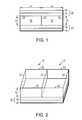
- FIG. 1is a schematic side sectional view of one embodiment of microcells of the invention.
- FIG. 2is a schematic top perspective view of the embodiment of FIG. 1 with several layers removed.
- FIG. 3is a depiction of fluid convection.
- the present inventionprovides materials and methods that improve performance of electrophoretic display devices.
- the present inventionprovides electrophoretic displays having a suspending fluid and particles that are contained in microcells of certain geometries. These microcells are disposed on a substrate with walls that define a void. The void can be filled with the suspending medium and particles.
- Microcells according to the inventionprovide displays with less particle agglomeration, less unwanted particle migration, better brightness, and/or better contrast than current displays. Moreover, the microcells have a shape that minimizes unwanted particle movement, occurring because of, for example, convective currents within the suspending medium within the cells.
- an electrophoretic suspensionis first formed.
- this suspensionis a darkly dyed oil, but, alternately, a suspending medium of any phase or visual property such as a clear medium, may be employed.
- Particles within the suspensionrespond to an electrostatic field to create different visual effects.
- this visual effectmay be accomplished. For example, white particles, located in a dark dye, can be located at the top of the suspension (towards a viewer) and appear white, or the particles can move to the bottom of the suspension (away from the viewer) and appear dark because they are obscured by the dark dye.
- the suspending mediumis clear and there are two or more species of particles, such as black and white particles, that move under different electric fields to create different visual effects.
- particlessuch as black and white particles
- electrophoretic display devicesare an array of electrophoretic cells.
- the cellsare separated by partitions that both prevent migration of particles and lend structural integrity to the display.
- such cellsare square and relatively large, about 1 mm or more in width.
- a bottom substrateis used to manufacture this type of device. Walls are formed to define the cells; liquid suspension is filled into the cells; and the array is sealed with a top layer.
- These cellular electrophoretic displayssuffer from manufacturing drawbacks, because an array of cells must be carefully filled with the electrophoretic suspension. Poor displays result from failure to fill all of the cells uniformly, improperly balancing the number of particles per cell, or permitting air to enter the system.
- an electrophoretic displayincludes a microcell that includes a bottom substrate, on which cell walls are formed, and a top substrate, which generally seals the interior of the cell.
- the cell walls and substratesdefine a microcell cavity into which an electrophoretic fluid can be filled.
- the electrophoretic fluidincludes one or more species of particle suspended in a suspending fluid.
- These microcellsfor example, absorb or scatter light.
- One exampleis a system in which the cells contain one or more species of electrophoretically mobile particles dispersed in a dyed suspending fluid.
- Another exampleis a system in which the cells contain two separate species of particles suspended in a clear suspending fluid, in which one species of particle absorbs light (dark), while the other species of particle scatters light (white). There are other extensions (more than two species of particles, with or without a dye, etc.).
- the particlesare commonly solid pigments, dyed particles, or pigment/polymer composites.
- the composition of the electrophoretic suspensioncan be controlled on a cell-by-cell level. As a result, for example, cyan, magenta and yellow colors can be metered out in an adjoining triad of microcells, permitting full color images to be displayed.
- a particleis any component that is charged or capable of acquiring a charge (i.e., has or is capable of acquiring electrophoretic mobility), and, in some cases, this mobility may be zero or close to zero (i.e., the particles will not move).
- the particlesmay be neat pigments, dyed (laked) pigments or pigment/polymer composites, or any other component that is charged or capable of acquiring a charge.
- Typical considerations for the electrophoretic particleare its optical properties, electrical properties, and surface chemistry.
- the particlesmay be organic or inorganic compounds, and they may either absorb light or scatter light.
- the particles for use in the inventionmay further include scattering pigments, absorbing pigments and luminescent particles.
- the particlesmay be retroreflective, such as comer cubes, or they may be electroluminescent, such as zinc sulfide particles, which emit light when excited by an AC field, or they may be photoluminescent.
- the particlesmay be surface treated so as to improve charging or interaction with a charging agent, or to improve dispersibility.
- titaniaOne particle for use in electrophoretic displays of the invention is titania.
- the titania particlesmay be coated with a metal oxide, such as aluminum oxide or silicon oxide, for example.
- the titania particlesmay have one, two, or more layers of metal-oxide coating.
- a titania particle for use in electrophoretic displays of the inventionmay have a coating of aluminum oxide and a coating of silicon oxide. The coatings may be added to the particle in any order.
- the electrophoretic particleis usually a pigment, a polymer, a laked pigment, or some combination of the above.
- a neat pigmentcan be any pigment, and, usually for a light colored particle, pigments such as rutile (titania), anatase (titania), barium sulfate, kaolin, or zinc oxide are useful. Some typical particles have high refractive indices, high scattering coefficients, and low absorption coefficients. Other particles are absorptive, such as carbon black or colored pigments used in paints and inks. The pigment should also be insoluble in the suspending fluid. Yellow pigments such as diarylide yellow, hansa yellow, and benzidin yellow have also found use in similar displays. Any other reflective material can be employed for a light colored particle, including non-pigment materials, such as metallic particles.
- Useful neat pigmentsinclude, but are not limited to, PbCrO 4 , Cyan blue GT 55-3295 (American Cyanamid Company, Wayne, N.J.), Cibacron Black BG (Ciba Company, Inc., Newport, Del.), Cibacron Turquoise Blue G (Ciba), Cibalon Black BGL (Ciba), Orasol Black BRG (Ciba), Orasol Black RBL (Ciba), Acetamine Blac, CBS (E. I. du Pont de Nemours and Company, Wilmington, Del.), Crocein Scarlet N Ex (E. I. du Pont de Nemours and Company) (27290), Fiber Black VF (E. I.
- du Pont de Nemours and Company(30235), Luxol Fast Black L (E. I. du Pont de Nemours and Company) (Solv. Black 17), Nirosine Base No. 424 (E. I. du Pont de Nemours and Company) (50415 B), Oil Black BG (E. I. du Pont de Nemours and Company) (Solv. Black 16), Rotalin Black RM (E. I. du Pont de Nemours and Company), Sevron Brilliant Red 3 B (E. I.
- Particlesmay also include laked, or dyed, pigments.
- Laked pigmentsare particles that have a dye precipitated on them or which are stained.
- Lakesare metal salts of readily soluble anionic dyes. These are dyes of azo, triphenylmethane or anthraquinone structure containing one or more sulphonic or carboxylic acid groupings. They are usually precipitated by a calcium, barium or aluminum salt onto a substrate. Typical examples are peacock blue lake (CI Pigment Blue 24) and Persian orange (lake of CI Acid Orange 7), Black M Toner (GAF) (a mixture of carbon black and black dye precipitated on a lake).
- CI Pigment Blue 24and Persian orange (lake of CI Acid Orange 7)
- GAFBlack M Toner
- a dark particle of the dyed typemay be constructed from any light absorbing material, such as carbon black, or inorganic black materials.
- the dark materialmay also be selectively absorbing.
- a dark green pigmentmay be used.
- Black particlesmay also be formed by staining latices with metal oxides, such latex copolymers consisting of any of butadiene, styrene, isoprene, methacrylic acid, methyl methacrylate, acrylonitrile, vinyl chloride, acrylic acid, sodium styrene sulfonate, vinyl acetate, chlorostyrene, dimethylaminopropylmethacrylamide, isocyanoethyl methacrylate and N(isobutoxymethacrylamide), and optionally including conjugated diene compounds such as diacrylate, triacrylate, dimethylacrylate and trimethacrylate.
- Black particlesmay also be formed by a dispersion polymerization technique.
- the pigments and polymersmay form multiple domains within the electrophoretic particle, or be aggregates of smaller pigment/polymer combined particles.
- a central pigment coremay be surrounded by a polymer shell.
- the pigment, polymer, or bothcan contain a dye.
- the optical purpose of the particlemay be to scatter light, absorb light, or both. Useful sizes may range from 1 nm up to about 100 ⁇ m, as long as the particles are smaller than the bounding microcell.
- the density of the electrophoretic particlemay be substantially matched to that of the suspending (i.e., electrophoretic) fluid.
- a suspending fluidhas a density that is “substantially matched” to the density of the particle if the difference in their respective densities is between about zero and about two grams/milliliter (“g/ml”). This difference is preferably between about zero and about 0.5 g/ml.
- Useful polymers for the particlesinclude, but are not limited to: polystyrene, polyethylene, polypropylene, phenolic resins, E. I. du Pont de Nemours and Company Elvax resins (ethylene-vinyl acetate copolymers), polyesters, polyacrylates, polymethacrylates, ethylene acrylic acid or methacrylic acid copolymers (Nucrel Resins—E. I. du Pont de Nemours and Company, Primacor Resins—Dow Chemical), acrylic copolymers and terpolymers (Elvacite Resins, E. I. du Pont de Nemours and Company) and PMMA.
- Useful materials for homopolymer/pigment phase separation in high shear meltinclude, but are not limited to, polyethylene, polypropylene, polymethylmethacrylate, polyisobutylmethacrylate, polystyrene, polybutadiene, polyisoprene, polyisobutylene, polylauryl methacrylate, polystearyl methacrylate, polyisobomyl methacrylate, poly-t-butyl methacrylate, polyethyl methacrylate, polymethyl acrylate, polyethyl acrylate, polyacrylonitrile, and copolymers of two or more of these materials.
- Some useful pigment/polymer complexesthat are commercially available include, but are not limited to, Process Magenta PM 1776 (Magruder Color Company, Inc., Elizabeth, N.J.), Methyl Violet PMA VM6223 (Magruder Color Company, Inc., Elizabeth, N.J.), and Naphthol FGR RF6257 (Magruder Color Company, Inc., Elizabeth, N.J.).
- the pigment-polymer compositemay be formed by a physical process, (e.g., attrition or ball milling), a chemical process (e.g., microencapsulation or dispersion polymerization), or any other process known in the art of particle production.
- a physical processe.g., attrition or ball milling
- a chemical processe.g., microencapsulation or dispersion polymerization
- any other process known in the art of particle productione.g., the processes and materials for both the fabrication of liquid toner particles and the charging of those particles may be relevant.
- liquid toners and microcell-bounded electrophoretic inksare similar, in that the pigment or dye must be easily incorporated therein, either by a physical, chemical, or physicochemical process, may aid in the colloidal stability, and may contain charging sites or may be able to incorporate materials which contain charging sites.
- One general requirement from the liquid toner industry that is not shared by microcell-bounded electrophoretic inksis that the toner must be capable of “fixing” the image, i.e., heat fusing together to create a uniform film after the deposition of the toner particles.
- Typical manufacturing techniques for particlesmay be drawn from the liquid toner and other arts and include ball milling, attrition, jet milling, etc.
- the processwill be illustrated for the case of a pigmented polymeric particle.
- the pigmentis compounded in the polymer, usually in some kind of high shear mechanism such as a screw extruder.
- the composite materialis then (wet or dry) ground to a starting size of around 10 ⁇ m. It is then dispersed in a carrier liquid, for example ISOPAR® (Exxon, Houston, Tex.), optionally with some charge control agent(s), and milled under high shear for several hours down to a final particle size and/or size distribution.
- a carrier liquidfor example ISOPAR® (Exxon, Houston, Tex.), optionally with some charge control agent(s), and milled under high shear for several hours down to a final particle size and/or size distribution.
- Another manufacturing technique for particlesis to add the polymer, pigment, and suspending fluid to a media mill.
- the millis started and simultaneously heated to temperature at which the polymer swells substantially with the solvent. This temperature is typically near 100° C. In this state, the pigment is easily encapsulated into the swollen polymer.
- the millis gradually cooled back to ambient temperature while stirring. The milling may be continued for some time to achieve a small enough particle size, typically a few micrometers in diameter.
- the charging agentsmay be added at this time.
- more suspending fluidmay be added.
- Chemical processessuch as dispersion polymerization, mini- or micro-emulsion polymerization, suspension polymerization precipitation, phase separation, solvent evaporation, in situ polymerization, seeded emulsion polymerization, or any process which falls under the general category of microencapsulation may be used.
- a typical process of this typeis a phase separation process wherein a dissolved polymeric material is precipitated out of solution onto a dispersed pigment surface through solvent dilution, evaporation, or a thermal change.
- Other processesinclude chemical means for staining polymeric latices, for example with metal oxides or dyes.
- the suspending fluid containing the particlescan be chosen based on properties such as density, refractive index, and solubility.
- a preferred suspending fluidhas a low dielectric constant (about 2), high volume resistivity (about 10 15 ohm-cm), low viscosity (less than 5 centistokes (“cst”)), parts per million (“ppm”)), high specific gravity (greater than 1.5), a high boiling point (greater than 90° C.), and a low refractive index (less than 1.2).
- suspending fluidmay be based on concerns of chemical inertness, density matching to the electrophoretic particle, or chemical compatibility with both the electrophoretic particle and bounding cell wall.
- the viscosity of the fluidshould be low when movement of the particles is desired.
- the refractive index of the suspending fluidmay also be substantially matched to that of the particles.
- the refractive index of a suspending fluid“is substantially matched” to that of a particle if the difference between their respective refractive indices is between about zero and about 0.3, and is preferably between about 0.05 and about 0.2.
- the fluidmay be chosen to be a poor solvent for some polymers, which is advantageous for use in the fabrication of microparticles, because it increases the range of polymeric materials useful in fabricating particles of polymers and pigments.
- Organic solventssuch as halogenated organic solvents, saturated linear or branched hydrocarbons, silicone oils, and low molecular weight halogen-containing polymers are some useful suspending fluids.
- the suspending fluidmay comprise a single fluid.
- the fluidwill, however, often be a blend of more than one fluid in order to tune its chemical and physical properties.
- the fluidmay contain surface modifiers to modify the surface energy or charge of the electrophoretic particle or bounding microcell. Reactants or solvents for the microcell wall forming process (oil soluble monomers, for example) can also be contained in the suspending fluid. Charge control agents can also be added to the suspending fluid.
- Useful organic solventsinclude, but are not limited to, epoxides, such as decane epoxide and dodecane epoxide; vinyl ethers, such as cyclohexyl vinyl ether and Decave® (International Flavors & Fragrances, Inc., New York, N.Y.); and aromatic hydrocarbons, such as toluene and naphthalene.
- Useful halogenated organic solventsinclude, but are not limited to, tetrafluorodibromoethylene, tetrachloroethylene, trifluorochloroethylene, 1,2,4-trichlorobenzene, carbon tetrachloride. These materials have high densities.
- Useful hydrocarbonsinclude, but are not limited to, dodecane, tetradecane, the aliphatic hydrocarbons in the Isopar® series (Exxon, Houston, Tex.), Norpar® (series of normal paraffinic liquids), Shell-Sol®(Shell, Houston, Tex.), and Sol-Trol® (Shell), naphtha, and other petroleum solvents. These materials usually have low densities.
- Useful examples of silicone oilsinclude, but are not limited to, octamethyl cyclosiloxane and higher molecular weight cyclic siloxanes, poly (methyl phenyl siloxane), hexamethyldisiloxane, and polydimethylsiloxane.
- halogen-containing polymersinclude, but are not limited to, poly(chlorotrifluoroethylene) polymer (Halogenated hydrocarbon Inc., River Edge, N.J.), Galden® (a perfluorinated ether from Ausimont, Morristown, N.J.), or Krytox® from E. I. du Pont de Nemours and Company (Wilmington, Del.).
- the suspending fluidis a poly(chlorotrifluoroethylene) polymer.
- this polymerhas a degree of polymerization from about 2 to about 10. Many of the above materials are available in a range of viscosities, densities, and boiling points.
- the fluidcan be capable of being formed into small droplets prior to a microcell being formed.
- Processes for forming small dropletsinclude flow-through jets, membranes, nozzles, or orifices, as well as shear-based emulsifying schemes.
- the formation of small dropsmay be assisted by electrical or sonic fields.
- Surfactants and polymerscan be used to aid in the stabilization and emulsification of the droplets.
- One surfactant for use in displays of the inventionis sodium dodecylsulfate.
- the suspending fluidcan contain an optically absorbing dye.
- This dyemust be soluble in the fluid, but will generally be insoluble in the other components of the microcell.
- the dyecan be a pure compound, or blends of dyes to achieve a particular color, including black.
- the dyescan be fluorescent, which would produce a display in which the fluorescence properties depend on the position of the particles.
- the dyescan be photoactive, changing to another color or becoming colorless upon irradiation with either visible or ultraviolet light, providing another means for obtaining an optical response. Dyes could also be polymerizable, forming a solid absorbing polymer inside the cell wall.
- dyesthat can be chosen for use in microcell electrophoretic displays. Properties important here include light fastness, solubility in the suspending liquid, color, and cost. These are generally from the class of azo, anthraquinone, and triphenylmethane type dyes and may be chemically modified so as to increase the solubility in the oil phase and reduce the adsorption by the particle surface.
- Useful azo dyesinclude, but are not limited to: the Oil Red dyes, and the Sudan Red and Sudan Black series of dyes.
- Useful anthraquinone dyesinclude, but are not limited to: the Oil Blue dyes, and the Macrolex Blue series of dyes.
- Useful triphenylmethane dyesinclude, but are not limited to, Michler's hydrol, Malachite Green, Crystal Violet, and Auramine O.
- Charge control agentsare used to provide good electrophoretic mobility to the electrophoretic particles.
- Stabilizersare used to prevent agglomeration of the electrophoretic particles, as well as prevent the electrophoretic particles from irreversibly depositing onto the microcell wall.
- Either componentcan be constructed from materials across a wide range of molecular weights (low molecular weight, oligomeric, or polymeric), and may be pure or a mixture.
- the charge control agent used to modify and/or stabilize the particle surface chargeis applied as generally known in the arts of liquid toners, electrophoretic displays, non-aqueous paint dispersions, and engine-oil additives. In all of these arts, charging species may be added to non-aqueous media in order to increase electrophoretic mobility or increase electrostatic stabilization. The materials can improve steric stabilization as well. Different theories of charging are postulated, including selective ion adsorption, proton transfer, and contact electrification.
- An optional charge control agent or charge directormay be used. These constituents typically consist of low molecular weight surfactants, polymeric agents, or blends of one or more components and serve to stabilize or otherwise modify the sign and/or magnitude of the charge on the electrophoretic particles.
- the charging properties of the pigment itselfmay be accounted for by taking into account the acidic or basic surface properties of the pigment, or the charging sites may take place on the carrier resin surface (if present), or a combination of the two. Additional pigment properties which may be relevant are the particle size distribution, the chemical composition, and the lightfastness.
- the charge control agent used to modify and/or stabilize the particle surface chargemay be applied as generally known in the arts of liquid toners, electrophoretic displays, non-aqueous paint dispersions, and engine-oil additives.
- charging speciesmay be added to non-aqueous media in order to increase electrophoretic mobility or increase electrostatic stabilization.
- the materialscan improve steric stabilization as well.
- Different theories of chargingare postulated, including selective ion adsorption, proton transfer, and contact electrification.
- Charge adjuvantsmay also be added. These materials increase the effectiveness of the charge control agents or charge directors.
- the charge adjuvantmay be a polyhydroxy compound or an aminoalcohol compound, which are preferably soluble in the suspending fluid in an amount of at least 2% by weight.
- polyhydroxy compounds which contain at least two hydroxyl groupsinclude, but are not limited to, ethylene glycol, 2,4,7,9-tetramethyl-decyne-4,7diol, poly (propylene glycol), pentaethylene glycol, tripropylene glycol, triethylene glycol, glycerol, pentaerythritol, glycerol tris(12-hydroxystearate), propylene glycerol monohydroxystearate, and ethylene glycol monohydroxystearate.
- the charge adjuvantis preferably present in the suspending fluid in an amount of about 1 to about 100 milligrams per gram (“mg/g”) of the particle mass, and more preferably about 50 to about 200 mg/g.
- the surface of the particlemay also be chemically modified to aid dispersion, to improve surface charge, and to improve the stability of the dispersion, for example.
- Surface modifiersinclude organic siloxanes, organohalogen silanes and other functional silane coupling agents (Dow Coming® Z-6070, Z-6124, and 3 additive, Midland, Mich.); organic titanates and zirconates (Tyzor® TOT, TBT, and TE Series, E. I.
- hydrophobing agentssuch as long chain (C12 to C50) alkyl and alkyl benzene sulphonic acids, fatty amines or diamines and their salts or quatenary derivatives; and amphipathic polymers which can be covalently bonded to the particle surface.
- chargingresults as an acid-base reaction between some moiety present in the continuous phase and the particle surface.
- useful materialsare those which are capable of participating in such a reaction, or any other charging reaction as known in the art.
- charge control agentswhich are useful include organic sulfates or sulfonates, metal soaps, block or comb copolymers, organic amides, organic zwitterions, and organic phosphates and phosphonates.
- Useful organic sulfates and sulfonatesinclude, but are not limited to, sodium bis(2-ethylhexyl) sulfosuccinate, calcium dodecyl benzene sulfonate, calcium petroleum sulfonate, neutral or basic barium dinonylnaphthalene sulfonate, neutral or basic calcium dinonylnaphthalene sulfonate, dodecylbenzenesulfonic acid sodium salt, and ammonium lauryl sulphate.
- Useful metal soapsinclude, but are not limited to, basic or neutral barium petronate, calcium petronate, Co-, Ca-, Cu-, Mn-, Ni-, Zn-, and Fe-salts of naphthenic acid, Ba-, Al-, Zn-, Cu-, Pb-, and Fe-salts of stearic acid, divalent and trivalent metal carboxylates, such as aluminum tristearate, aluminum octanoate, lithium heptanoate, iron stearate, iron distearate, barium stearate, chromium stearate, magnesium octanoate, calcium stearate, iron naphthenate, and zinc naphthenate, Mn- and Zn-heptanoate, and Ba-, Al-, Co-, Mn-, and Zn-octanoate.
- Useful block or comb copolymersinclude, but are not limited to, AB diblock copolymers of (A) polymers of 2-(N,N)-dimethylaminoethyl methacrylate quatemized with methyl-p-toluenesulfonate and (B) poly-2-ethylhexyl methacrylate, and comb graft copolymers with oil soluble tails of poly (12-hydroxystearic acid) and having a molecular weight of about 1800, pendant on an oil-soluble anchor group of poly (methyl methacrylate-methacrylic acid).
- Useful organic amidesinclude, but are not limited to, polyisobutylene succinimides such as OLOA 1200, and N-vinyl pyrrolidone polymers.
- Useful organic zwitterionsinclude, but are not limited to, lecithin.
- Useful organic phosphates and phosphonatesinclude, but are not limited to, the sodium salts of phosphated mono- and di-glycerides with saturated and unsaturated acid substituents.
- Particle dispersion stabilizersmay be added to prevent particle flocculation or attachment to the microcell walls.
- nonaqueous surfactantsinclude, but are not limited to, glycol ethers, acetylenic glycols, alkanolarnides, sorbitol derivatives, alkyl amines, quaternary amines, imidazolines, dialkyl oxides, and sulfosuccinates.
- microcells 10 , 12are disposed adjacent, and partially defined by, a bottom substrate 20 .
- the bottom substrate 20has several layers 16 , 18 , a base layer 16 and an electrode 18 .
- the base layer 16forms the bottom of the microcells 10 , 12 , and interfaces with the walls 22 surrounding the cells 10 , 12 .
- the electrode 18(such as a control grid) is adjacent the base layer 16 .
- a top substrate 26is located opposite the bottom substrate 20 , and is made of several layers 14 , 24 , a top layer 14 , that seals the top of the microcells 10 , 12 , and a second electrode 24 .
- this embodimentis shown having two substrates 20 , 26 , each with two layers, alternative embodiments can have fewer or more layers, depending upon the materials used.
- the cell walls 22can be directly formed on an electrode and sealed with a second electrode, forming a substrate with only one layer.
- the microcells 10 , 12have a height (h) and a width (w). The width (w) is measured along the substrate 20 , as described in the following paragraph.
- microcellshave a hollow cavity defined by the cell walls and at least one of the substrates. The particles, suspending medium, and/or charge control agents and particle stabilizers are loaded into the interior cavity of the microcell.
- Microcells of the inventioncan utilize a variety of shapes and are relatively small.
- the microcellspreferably are square in shape (as shown in the top perspective view of FIG. 2) and arranged in a matrix. Such microcells are about 5 micrometers to about 200 micrometers wide, preferably about 10 micrometers to about 100 micrometers wide.
- the terms ‘wide’ and ‘width’,refer to the greatest dimension of the microcell. For example, the ‘width’ of a square microcell is 2 times the length of a side of the square and the ‘width’ of a circular microcell is the diameter of the circle.
- FIG. 3depicts a fluid layer bounded by substrates 20 ′ and 26 ′. Three double rolls are depicted and the wavelength, ⁇ , of one double roll is indicated, ⁇ being equal to two times the height. Each “roll” in the double roll is seen to engage in mirror image, circular motion.
- width of the microcell cavitycan be no more than about three times, and preferably no more than two times, the height of the microcell cavity.
- the cell wallsprovide a substantial impediment to the creation and motion of the above described rolling effect.
- the precise width at which a desirable effect is achievedwill vary somewhat with the particular choice of fluid and the particular choice of microcell shape. Width, as described above, refers to lateral dimensions along a bottom substrate (which can be an electrode), whereas height, as described above, refers to the height of the cell wall which correlates with the gap between top and bottom substrates (such as two electrodes.)
- microcell shapecan be varied to obtain varying effects on motion of fluid in the microcell.
- a square shapeis desirable for manufacturing purposes and visual performance of a display
- other microcell shapescan be employed.
- a very irregular shapecan be employed, such that the width, as defined above, is greater than three times the cell height with fluid motion that is still effectively damped.
- Such an irregularly-shaped microcellwould have limited utility for use in a display.
- the walls used to separate the microcellsconstitute areas of the display that do not generate a visual effect, reducing the aperture ratio of the display. That is, any of the cell walls are areas of a display that are not visually active and detract from the uniformity of a changeable display. By keeping the walls as thin as possible, the amount of changeable viewing surface is maximized and the display does not suffer from having a minimal amount of visually inactive areas. Thus, the walls should be as thin as possible while still ensuring structural integrity, and the microcells should be as wide as possible without permitting unfortunate hydrodynamic flows.
- a dye-based electrophoretic systemis constructed from microcells that are about 50 micrometers high and about 120 micrometers wide.
- an electrophoretic system employing a clear medium in which two species of contrasting particles are suspendedis constructed of microcel is that are about 20 micrometers high and that are about 50 micrometers wide.
- the microcell wallscan be formed by photolithography methods and are less than about 10 micrometers wide, and are preferably about 3 micrometers to about 5 micrometers wide.
- any suitable material and manufacturing techniquemay be employed.
- a variety of methodsmay be used, including additive methods that create walls upon a substrate, subtractive methods that hollow wells within a substrate, or a combination thereof.
- Microcell wallscan be formed with techniques such as microprinting, photolithography, sandblasting, screenprinting, vacuum deposition, electron beam curing, laser etching including excimer laser etching, chemical etching, curing by radiation including ultraviolet light, infrared etching, and/or stereolithography.
- methods and materials useful in the art of manufacturing plasma display panel barrier ribscan be used.
- Methods that are capable of making short wallscan, in some cases, be repeated to build up a taller wall.
- each microcell layerhas a wall that is a fraction of the desired final microcell height, and the two layers are combined which, together, form a wall of the desired final height.
- This stepcan be preceded by other steps.
- a glue or conductive electrodecan be inserted on the cell walls, in the cavities defined by the microcells, or on the sides of the walls of the microcell cavities.
- These stepsfacilitate forming a control grid structure for addressing and controlling an electrophoretic display.
- a gridis formed and then adhered to a substrate that forms the bottom or top of the microcell.
- the gridmay be fashioned, for example, with a technique such as etching, punching, slitting and stretching, or stamping a substrate.
- This gridtypically is formed from overlapping rows and columns of a conductive or semiconductive material.
- a polymeris embossed onto a substrate to create a micro-ribbed structure.
- narrow, hollow tubeshaving the desired width are extruded or otherwise suitably created.
- a group of strawsare collected and bundled such that they are substantially parallel to each other.
- the strawsshould be closely packed, which can be achieved by applying pressure to the straws.
- the strawscan be bonded together by any suitable means, such as heating the straws.
- the ends of the strawsthen are sliced, for example with a laser, such that a thin (of the desired height) grid of closely-packed walls is thereby created.
- the microcellsare filled with an electrophoretic suspension, and the microcells are sealed.
- this electrophoretic suspensionincludes at least a suspending fluid and particles.
- Many alternative suspensions and components of these suspensionsare described above in more detail. Many techniques can be used to fill the microcells, however, these techniques should achieve a homogeneous electrophoretic suspension and minimize entry of air into the system.
- an electrophoretic suspensionis poured across the array of microcells to fill the cells. Then, a top substrate is positioned over the open end of the array (assuming that the microcells are already attached to a bottom substrate), and a roller presses the layers together.
- the rollersqueezes excess electrophoretic suspension, as well as air, out of the microcell cavities as it proceeds from one end of the array to the other.
- the step of removing excess electrophoretic suspension and aircan be accomplished as part of a laminating step, or it may be closely followed by a bonding step.
- gluemay be applied across the top of the microcell walls. Alternately, less or no glue is used, except around the edges of the display, and top layer is held against the microcell walls with the tension of an outer seal.
- Metered inkjet deposition, screenprinting, or other coating and printing methodscan be used to fill the microcell cavities, although not all inkjet methods are viable. If the electrophoretic display suspension is an oil, then inkjet heads that operate by heating an aqueous liquid are not useful. One embodiment employs an inkjet head that operates using piezoelectric elements. Alternately, any metering method can be used to fill the cells, including a nozzle dispensing the electrophoretic suspension under pressure or gravity.
- one of the substratesis a porous material, such as a nuclear pore filter material, that permits the electrophoretic medium, such as oil, to flow through the material but prevents the particles from flowing through the material.
- a porous materialsuch as a nuclear pore filter material
- Such a systempermits a variety of filling methods. For example, microcells are formed on a bottom porous substrate. A dusting of particles is applied across the entire substrate (from the top) in a substantially homogeneous manner, such that particles are located within microcell cavities. Masks can be employed such that specific cells are dusted with specific colored particles. A non-porous top substrate then is laid across the microcells and bonded to the tops of the cell walls.
- a vacuumis applied, voiding the system of air but not voiding the system of particles because the particles are too large to pass through the porous layer.
- a liquid electrophoretic mediumsuch as an oil.
- the oilcan be introduced into the preformed cell by capillary action or vacuum pressure.
- the oilenters the cavities of each microcell through the porous bottom substrate.
- the porous bottom substratethen is wiped to remove excess material.
- a non-porous membranethen is laminated or bonded to the bottom substrate, such that the microcells are fully bounded and substantially impermeable to the oil and particles.
- the array of microcellscan be inserted into a chamber that is filled with a hot vapor.
- the vaporcondenses, it forms the electrophoretic display medium in the cavities of the microcells.
- a chilling devicecan be employed to further control the condensing process.
- both the top and bottom substratesare porous.
- the systemis dipped into a suspending medium such as oil, which enters the cells through both porous layers, and remains in the microcells, by capillary action.
- the systemthen is laminated between a top, non-porous layer and a bottom, 5 non-porous layer to prevent the exit of the suspending medium.
- the top substratebefore it is applied to the top of the microcell walls, can be coated with an uncured polymer that is not soluble in the electrophoretic suspending medium to be used.
- a curing mechanismsuch as heat or ultraviolet light, cures the polymer and fuses the top substrate to the microcell walls.
- Another method of filling the microcell cavitiesuses a bottom and top substrate.
- One or both of the substratesinclude a fraction of the desired final height of the microcell wall.
- the two substratesare brought together, while submerged in a bath of the electrophoretic suspension, typically with stirring to achieve a homogeneous particle distribution.
- a forming devicepinches off rows of microcells such that each microcell contains the electrophoretic suspension.
- the microcellsare made permanent by sealing the two substrates together with pressure or by bonding the two substrates with heat, radiation, glue and/or pressure. If neither of the two substrates have a fraction of the microcell wall, microcells can be formed in a manner similar to the operation of a waffle iron. For example, the two substrates are squeezed together in a mold and fused along a grid-like pattern.
- the filling and sealing steps for individual microcellsare avoided by forming the display as one pocket that is filled and scaled. Then, the microcell walls are formed in situ post facto. For example, a suitable polymer is added to the electrophoretic display suspension. After the pocket is filled and sealed, electrodes in a grid-like pattern are employed under alternating current to cause the polymer to dielectrophoretically collect together in a pattern matching the electrode grid pattern. Once in position, the polymer is fused by any suitable means to form the cell wall. Alternatively, the polymer can be formed by a phase separation (i.e., thermal, solvent evaporative, or radiation induced) process such that the cavities formed in the polymer matrix have the appropriate aspect ratios of height to width.
- a phase separationi.e., thermal, solvent evaporative, or radiation induced
- Another alternative method for forming walls in situis to add an additional species of particle to the electrophoretic display suspension that will respond to an applied field pattern to form the walls. For example, large magnetically responsive particles incorporating a polymer are added. The particles respond to an external magnetic pattern to migrate to the wall locations (as determined by the magnetic pattern). Again, the walls are fused together and act as stable walls, for example, with thermal energy.
- electrostatic display mediarefers to a filled and sealed microcell structure having top and bottom substrates that is capable, when appropriately addressed, of imaging desired visual effects.
Landscapes
- Physics & Mathematics (AREA)
- Nonlinear Science (AREA)
- Health & Medical Sciences (AREA)
- Life Sciences & Earth Sciences (AREA)
- Chemical & Material Sciences (AREA)
- Chemical Kinetics & Catalysis (AREA)
- Electrochemistry (AREA)
- Molecular Biology (AREA)
- General Physics & Mathematics (AREA)
- Optics & Photonics (AREA)
- Electrochromic Elements, Electrophoresis, Or Variable Reflection Or Absorption Elements (AREA)
Abstract
Description
The present application claims priority to and the benefit of U.S. provisional patent application serial No. 60/127,965, filed Apr. 6, 1999, the contents of which are incorporated herein by reference.
The present invention generally relates to electrophoretic displays and, in particular, to electrophoretic displays using microcells.
A variety of electronic display devices operate by the principle of electrophoresis. In such displays, an electrophoretic suspension contains electrophoretically mobile particles. Many electrophoretic displays suffer from several failure modes. In one failure mode, the particles stick or agglomerate together and the desired visual effect is reduced. In another failure mode, the particles migrate across the face of the display (particularly under the influence of gravity). Both of these failure modes result in a nonuniform display.
As such, current electrophoretic display technology produces a display that neither is as bright nor has as much contrast as is desired. Current displays are not capable of achieving uniform brightness or good contrast due to limitations in their construction. Thus, new materials and methods of construction are needed to provide electrophoretic displays with acceptable brightness and contrast.
The present invention provides electrophoretic displays having a suspending fluid and particles that are contained in microcells of certain geometries. These microcells are disposed on a substrate with walls that define a void. The void can be filled with a suspending medium and particles. Microcells according to the invention provide displays with less particle agglomeration, less unwanted particle migration, better brightness, and/or better contrast than current displays.
Throughout the Specification, the invention is described as a display or an array for ease of description. However, the compositions and processes disclosed herein are equally applicable to “elements”. A display or an array are examples of the broader concept of an element. One or more elements can be ordered into a display, array, or other articles of manufacture. Elements can include any of the features described for a display or an array. As used herein, “cell” and “microcell” are used interchangeably, unless otherwise specified, or otherwise apparent from context. Also, as used herein, “suspending fluid” and “suspending medium” are used interchangeably, unless otherwise specified, or otherwise apparent from context.
Generally, particles move within the microcell under the influence of a voltage. Depending upon the location of the particles and the composition of the suspending fluid, various visual states are available. In one highly generalized example, reflecting particles, located at the front of the cell (towards a viewer) in a colored dye, will reflect light and appear “white.” When the reflecting particles move towards the rear of the cell (opposite the viewer) upon application of an electric, the particles will be obscured by the dyed fluid and will appear “dark” to a viewer.
In one aspect of the invention, an electrophoretic display element includes at least one substrate and at least one cell that is defined by a cell wall and that is disposed on the substrate. The cell has a width that is not greater than about three times a height of the cell wall, preferably from about two to about three time the height of the cell wall.
The electrophoretic display element can have any of the following features. A cell wall can be less than 10 micrometers wide. The substrate can include a control grid electrode structure, and the cell can include two laminated structures. The cell wall can be formed at least in part with a technique such as photolithography, sandblasting, screenprinting, embossing, laser etching or radiation curing. The substrate can be permeable to a suspending fluid and substantially impermeable to electrophoretic particles, such that the suspending fluid and the particles fill a cavity defined by the cell walls. The substrate can be coated with a polymer, and the polymer can be insoluble in a suspending medium contained within a cavity defined by the cell walls. A suspending fluid contained within a cavity defined by the cell walls can be a substantially clear liquid.
In another aspect of the invention, an electrophoretic display element includes a substrate and at least one cell defined by a cell wall and disposed on the substrate. The cell contains a suspending medium and a plurality of electrophoretic particles, and the cell has a shape that minimizes hydrodynamic motion within the suspending medium within the cell. The hydrodynamic motion can be caused by, for example, convective currents within the suspending medium within the cell.
The invention, in accordance with preferred and exemplary embodiments, together with further advantages thereof, is more particularly described in the following detailed description, taken in conjunction with the accompanying drawings.
In the drawings, like reference characters generally refer to the same parts throughout the different views. Also, the drawings are not necessarily to scale, emphasis instead generally being placed upon illustrating principles of the invention.
FIG. 1 is a schematic side sectional view of one embodiment of microcells of the invention.
FIG. 2 is a schematic top perspective view of the embodiment of FIG. 1 with several layers removed.
FIG. 3 is a depiction of fluid convection.
The present invention provides materials and methods that improve performance of electrophoretic display devices. The present invention provides electrophoretic displays having a suspending fluid and particles that are contained in microcells of certain geometries. These microcells are disposed on a substrate with walls that define a void. The void can be filled with the suspending medium and particles. Microcells according to the invention provide displays with less particle agglomeration, less unwanted particle migration, better brightness, and/or better contrast than current displays. Moreover, the microcells have a shape that minimizes unwanted particle movement, occurring because of, for example, convective currents within the suspending medium within the cells.
Many electronic display devices operate by the principle of electrophoresis. In such displays, an electrophoretic suspension is first formed. Typically, this suspension is a darkly dyed oil, but, alternately, a suspending medium of any phase or visual property such as a clear medium, may be employed. Particles within the suspension respond to an electrostatic field to create different visual effects. There are different means by which this visual effect may be accomplished. For example, white particles, located in a dark dye, can be located at the top of the suspension (towards a viewer) and appear white, or the particles can move to the bottom of the suspension (away from the viewer) and appear dark because they are obscured by the dark dye. In other displays, the suspending medium is clear and there are two or more species of particles, such as black and white particles, that move under different electric fields to create different visual effects. Many of these electrophoretic displays, and particularly those that utilize relatively large cells, suffer from several failure modes. In one failure mode, the particles stick or agglomerate together and the desired visual effect is reduced. In another failure mode, the particles migrate across the face of the display (particularly under the influence of gravity). Both of these failure modes result in a nonuniform display.
Many current electrophoretic display devices are an array of electrophoretic cells. The cells are separated by partitions that both prevent migration of particles and lend structural integrity to the display. Typically, such cells are square and relatively large, about 1 mm or more in width. To manufacture this type of device, a bottom substrate is used. Walls are formed to define the cells; liquid suspension is filled into the cells; and the array is sealed with a top layer. These cellular electrophoretic displays suffer from manufacturing drawbacks, because an array of cells must be carefully filled with the electrophoretic suspension. Poor displays result from failure to fill all of the cells uniformly, improperly balancing the number of particles per cell, or permitting air to enter the system.
Generally, according to the invention, an electrophoretic display includes a microcell that includes a bottom substrate, on which cell walls are formed, and a top substrate, which generally seals the interior of the cell. The cell walls and substrates define a microcell cavity into which an electrophoretic fluid can be filled. In one embodiment, the electrophoretic fluid includes one or more species of particle suspended in a suspending fluid. These microcells, for example, absorb or scatter light. One example is a system in which the cells contain one or more species of electrophoretically mobile particles dispersed in a dyed suspending fluid. Another example is a system in which the cells contain two separate species of particles suspended in a clear suspending fluid, in which one species of particle absorbs light (dark), while the other species of particle scatters light (white). There are other extensions (more than two species of particles, with or without a dye, etc.). The particles are commonly solid pigments, dyed particles, or pigment/polymer composites. Moreover, the composition of the electrophoretic suspension can be controlled on a cell-by-cell level. As a result, for example, cyan, magenta and yellow colors can be metered out in an adjoining triad of microcells, permitting full color images to be displayed.
A. Particles
There is much flexibility in the choice of particles for use in electrophoretic displays, as described above. For purposes of this invention, a particle is any component that is charged or capable of acquiring a charge (i.e., has or is capable of acquiring electrophoretic mobility), and, in some cases, this mobility may be zero or close to zero (i.e., the particles will not move). The particles may be neat pigments, dyed (laked) pigments or pigment/polymer composites, or any other component that is charged or capable of acquiring a charge. Typical considerations for the electrophoretic particle are its optical properties, electrical properties, and surface chemistry. The particles may be organic or inorganic compounds, and they may either absorb light or scatter light. The particles for use in the invention may further include scattering pigments, absorbing pigments and luminescent particles. The particles may be retroreflective, such as comer cubes, or they may be electroluminescent, such as zinc sulfide particles, which emit light when excited by an AC field, or they may be photoluminescent. Finally, the particles may be surface treated so as to improve charging or interaction with a charging agent, or to improve dispersibility.
One particle for use in electrophoretic displays of the invention is titania. The titania particles may be coated with a metal oxide, such as aluminum oxide or silicon oxide, for example. The titania particles may have one, two, or more layers of metal-oxide coating. For example, a titania particle for use in electrophoretic displays of the invention may have a coating of aluminum oxide and a coating of silicon oxide. The coatings may be added to the particle in any order.
The electrophoretic particle is usually a pigment, a polymer, a laked pigment, or some combination of the above. A neat pigment can be any pigment, and, usually for a light colored particle, pigments such as rutile (titania), anatase (titania), barium sulfate, kaolin, or zinc oxide are useful. Some typical particles have high refractive indices, high scattering coefficients, and low absorption coefficients. Other particles are absorptive, such as carbon black or colored pigments used in paints and inks. The pigment should also be insoluble in the suspending fluid. Yellow pigments such as diarylide yellow, hansa yellow, and benzidin yellow have also found use in similar displays. Any other reflective material can be employed for a light colored particle, including non-pigment materials, such as metallic particles.
Useful neat pigments include, but are not limited to, PbCrO4, Cyan blue GT 55-3295 (American Cyanamid Company, Wayne, N.J.), Cibacron Black BG (Ciba Company, Inc., Newport, Del.), Cibacron Turquoise Blue G (Ciba), Cibalon Black BGL (Ciba), Orasol Black BRG (Ciba), Orasol Black RBL (Ciba), Acetamine Blac, CBS (E. I. du Pont de Nemours and Company, Wilmington, Del.), Crocein Scarlet N Ex (E. I. du Pont de Nemours and Company) (27290), Fiber Black VF (E. I. du Pont de Nemours and Company) (30235), Luxol Fast Black L (E. I. du Pont de Nemours and Company) (Solv. Black 17), Nirosine Base No. 424 (E. I. du Pont de Nemours and Company) (50415 B), Oil Black BG (E. I. du Pont de Nemours and Company) (Solv. Black 16), Rotalin Black RM (E. I. du Pont de Nemours and Company), Sevron Brilliant Red 3 B (E. I. du Pont de Nemours and Company); Basic Black DSC (Dye Specialties, Inc.), Hectolene Black (Dye Specialties, Inc.), Azosol Brilliant Blue B (GAF, Dyestuff and Chemical Division, Wayne, N.J.) (Solv. Blue 9), Azosol Brilliant Green BA (GAF) (Solv. Green 2), Azosol Fast Brilliant Red B (GAF), Azosol Fast Orange RA Conc. (GAF) (Solv. Orange 20), Azosol Fast Yellow GRA Conc. (GAF) (13900 A), Basic Black KMPA (GAF), Benzofix Black CW-CF (GAF) (35435), Cellitazol BNFV Ex Soluble CF (GAF) (Disp. Black 9), Celliton Fast Blue AF Ex Conc (GAF) (Disp. Blue 9), Cyper Black IA (GAF) (Basic Blk. 3), Diamine Black CAP Ex Conc (GAF) (30235), Diamond Black EAN Hi Con. CF (GAF) (15710), Diamond Black PBBA Ex (GAF) (16505); Direct Deep Black EA Ex CF (GAF) (30235), Hansa Yellow G (GAF) (11680); Indanthrene Black BBK Powd. (GAF) (59850), Indocarbon CLGS Conc. CF (GAF) (53295), Katigen Deep Black NND Hi Conc. CF (GAF) (15711), Rapidogen Black 3 G (GAF) (Azoic Blk. 4); Sulphone Cyanine Black BA-CF (GAF) (26370), Zambezi Black VD Ex Conc. (GAF) (30015); Rubanox Red CP-1495 (The Sherwin-Williams Company, Cleveland, Ohio) (15630); Raven 11 (Columbian Carbon Company, Atlanta, Ga.), (carbon black aggregates with a particle size of about 25 μm), Statex B-12 (Columbian Carbon Co.) (a furnace black of 33 μm average particle size), and chrome green.
Particles may also include laked, or dyed, pigments. Laked pigments are particles that have a dye precipitated on them or which are stained. Lakes are metal salts of readily soluble anionic dyes. These are dyes of azo, triphenylmethane or anthraquinone structure containing one or more sulphonic or carboxylic acid groupings. They are usually precipitated by a calcium, barium or aluminum salt onto a substrate. Typical examples are peacock blue lake (CI Pigment Blue 24) and Persian orange (lake of CI Acid Orange 7), Black M Toner (GAF) (a mixture of carbon black and black dye precipitated on a lake).
A dark particle of the dyed type may be constructed from any light absorbing material, such as carbon black, or inorganic black materials. The dark material may also be selectively absorbing. For example, a dark green pigment may be used. Black particles may also be formed by staining latices with metal oxides, such latex copolymers consisting of any of butadiene, styrene, isoprene, methacrylic acid, methyl methacrylate, acrylonitrile, vinyl chloride, acrylic acid, sodium styrene sulfonate, vinyl acetate, chlorostyrene, dimethylaminopropylmethacrylamide, isocyanoethyl methacrylate and N(isobutoxymethacrylamide), and optionally including conjugated diene compounds such as diacrylate, triacrylate, dimethylacrylate and trimethacrylate. Black particles may also be formed by a dispersion polymerization technique.
In the systems containing pigments and polymers, the pigments and polymers may form multiple domains within the electrophoretic particle, or be aggregates of smaller pigment/polymer combined particles. Alternatively, a central pigment core may be surrounded by a polymer shell. The pigment, polymer, or both can contain a dye. The optical purpose of the particle may be to scatter light, absorb light, or both. Useful sizes may range from 1 nm up to about 100 μm, as long as the particles are smaller than the bounding microcell. The density of the electrophoretic particle may be substantially matched to that of the suspending (i.e., electrophoretic) fluid. As defined herein, a suspending fluid has a density that is “substantially matched” to the density of the particle if the difference in their respective densities is between about zero and about two grams/milliliter (“g/ml”). This difference is preferably between about zero and about 0.5 g/ml.
Useful polymers for the particles include, but are not limited to: polystyrene, polyethylene, polypropylene, phenolic resins, E. I. du Pont de Nemours and Company Elvax resins (ethylene-vinyl acetate copolymers), polyesters, polyacrylates, polymethacrylates, ethylene acrylic acid or methacrylic acid copolymers (Nucrel Resins—E. I. du Pont de Nemours and Company, Primacor Resins—Dow Chemical), acrylic copolymers and terpolymers (Elvacite Resins, E. I. du Pont de Nemours and Company) and PMMA. Useful materials for homopolymer/pigment phase separation in high shear melt include, but are not limited to, polyethylene, polypropylene, polymethylmethacrylate, polyisobutylmethacrylate, polystyrene, polybutadiene, polyisoprene, polyisobutylene, polylauryl methacrylate, polystearyl methacrylate, polyisobomyl methacrylate, poly-t-butyl methacrylate, polyethyl methacrylate, polymethyl acrylate, polyethyl acrylate, polyacrylonitrile, and copolymers of two or more of these materials. Some useful pigment/polymer complexes that are commercially available include, but are not limited to, Process Magenta PM 1776 (Magruder Color Company, Inc., Elizabeth, N.J.), Methyl Violet PMA VM6223 (Magruder Color Company, Inc., Elizabeth, N.J.), and Naphthol FGR RF6257 (Magruder Color Company, Inc., Elizabeth, N.J.).
The pigment-polymer composite may be formed by a physical process, (e.g., attrition or ball milling), a chemical process (e.g., microencapsulation or dispersion polymerization), or any other process known in the art of particle production. For example, the processes and materials for both the fabrication of liquid toner particles and the charging of those particles may be relevant.
New and useful electrophoretic particles may still be discovered, but a number of particles already known to those skilled in the art of electrophoretic displays and liquid toners can also prove useful. In general, the polymer requirements for liquid toners and microcell-bounded electrophoretic inks are similar, in that the pigment or dye must be easily incorporated therein, either by a physical, chemical, or physicochemical process, may aid in the colloidal stability, and may contain charging sites or may be able to incorporate materials which contain charging sites. One general requirement from the liquid toner industry that is not shared by microcell-bounded electrophoretic inks is that the toner must be capable of “fixing” the image, i.e., heat fusing together to create a uniform film after the deposition of the toner particles.
Typical manufacturing techniques for particles may be drawn from the liquid toner and other arts and include ball milling, attrition, jet milling, etc. The process will be illustrated for the case of a pigmented polymeric particle. In such a case the pigment is compounded in the polymer, usually in some kind of high shear mechanism such as a screw extruder. The composite material is then (wet or dry) ground to a starting size of around 10 μm. It is then dispersed in a carrier liquid, for example ISOPAR® (Exxon, Houston, Tex.), optionally with some charge control agent(s), and milled under high shear for several hours down to a final particle size and/or size distribution.
Another manufacturing technique for particles is to add the polymer, pigment, and suspending fluid to a media mill. The mill is started and simultaneously heated to temperature at which the polymer swells substantially with the solvent. This temperature is typically near 100° C. In this state, the pigment is easily encapsulated into the swollen polymer. After a suitable time, typically a few hours, the mill is gradually cooled back to ambient temperature while stirring. The milling may be continued for some time to achieve a small enough particle size, typically a few micrometers in diameter. The charging agents may be added at this time. Optionally, more suspending fluid may be added.
Chemical processes such as dispersion polymerization, mini- or micro-emulsion polymerization, suspension polymerization precipitation, phase separation, solvent evaporation, in situ polymerization, seeded emulsion polymerization, or any process which falls under the general category of microencapsulation may be used. A typical process of this type is a phase separation process wherein a dissolved polymeric material is precipitated out of solution onto a dispersed pigment surface through solvent dilution, evaporation, or a thermal change. Other processes include chemical means for staining polymeric latices, for example with metal oxides or dyes.
B. Suspending Fluid
The suspending fluid containing the particles can be chosen based on properties such as density, refractive index, and solubility. A preferred suspending fluid has a low dielectric constant (about 2), high volume resistivity (about 1015ohm-cm), low viscosity (less than 5 centistokes (“cst”)), parts per million (“ppm”)), high specific gravity (greater than 1.5), a high boiling point (greater than 90° C.), and a low refractive index (less than 1.2).
The choice of suspending fluid may be based on concerns of chemical inertness, density matching to the electrophoretic particle, or chemical compatibility with both the electrophoretic particle and bounding cell wall. The viscosity of the fluid should be low when movement of the particles is desired. The refractive index of the suspending fluid may also be substantially matched to that of the particles. As used herein, the refractive index of a suspending fluid “is substantially matched” to that of a particle if the difference between their respective refractive indices is between about zero and about 0.3, and is preferably between about 0.05 and about 0.2.
Additionally, the fluid may be chosen to be a poor solvent for some polymers, which is advantageous for use in the fabrication of microparticles, because it increases the range of polymeric materials useful in fabricating particles of polymers and pigments. Organic solvents, such as halogenated organic solvents, saturated linear or branched hydrocarbons, silicone oils, and low molecular weight halogen-containing polymers are some useful suspending fluids. The suspending fluid may comprise a single fluid. The fluid will, however, often be a blend of more than one fluid in order to tune its chemical and physical properties. Furthermore, the fluid may contain surface modifiers to modify the surface energy or charge of the electrophoretic particle or bounding microcell. Reactants or solvents for the microcell wall forming process (oil soluble monomers, for example) can also be contained in the suspending fluid. Charge control agents can also be added to the suspending fluid.
Useful organic solvents include, but are not limited to, epoxides, such as decane epoxide and dodecane epoxide; vinyl ethers, such as cyclohexyl vinyl ether and Decave® (International Flavors & Fragrances, Inc., New York, N.Y.); and aromatic hydrocarbons, such as toluene and naphthalene. Useful halogenated organic solvents include, but are not limited to, tetrafluorodibromoethylene, tetrachloroethylene, trifluorochloroethylene, 1,2,4-trichlorobenzene, carbon tetrachloride. These materials have high densities. Useful hydrocarbons include, but are not limited to, dodecane, tetradecane, the aliphatic hydrocarbons in the Isopar® series (Exxon, Houston, Tex.), Norpar® (series of normal paraffinic liquids), Shell-Sol®(Shell, Houston, Tex.), and Sol-Trol® (Shell), naphtha, and other petroleum solvents. These materials usually have low densities. Useful examples of silicone oils include, but are not limited to, octamethyl cyclosiloxane and higher molecular weight cyclic siloxanes, poly (methyl phenyl siloxane), hexamethyldisiloxane, and polydimethylsiloxane. These materials usually have low densities. Useful low molecular weight halogen-containing polymers include, but are not limited to, poly(chlorotrifluoroethylene) polymer (Halogenated hydrocarbon Inc., River Edge, N.J.), Galden® (a perfluorinated ether from Ausimont, Morristown, N.J.), or Krytox® from E. I. du Pont de Nemours and Company (Wilmington, Del.). In a preferred embodiment, the suspending fluid is a poly(chlorotrifluoroethylene) polymer. In a particularly preferred embodiment, this polymer has a degree of polymerization from about 2 to about 10. Many of the above materials are available in a range of viscosities, densities, and boiling points.
The fluid can be capable of being formed into small droplets prior to a microcell being formed. Processes for forming small droplets include flow-through jets, membranes, nozzles, or orifices, as well as shear-based emulsifying schemes. The formation of small drops may be assisted by electrical or sonic fields. Surfactants and polymers can be used to aid in the stabilization and emulsification of the droplets. One surfactant for use in displays of the invention is sodium dodecylsulfate.
It can be advantageous in some displays for the suspending fluid to contain an optically absorbing dye. This dye must be soluble in the fluid, but will generally be insoluble in the other components of the microcell. There is much flexibility in the choice of dye material. The dye can be a pure compound, or blends of dyes to achieve a particular color, including black. The dyes can be fluorescent, which would produce a display in which the fluorescence properties depend on the position of the particles. The dyes can be photoactive, changing to another color or becoming colorless upon irradiation with either visible or ultraviolet light, providing another means for obtaining an optical response. Dyes could also be polymerizable, forming a solid absorbing polymer inside the cell wall.
There are many dyes that can be chosen for use in microcell electrophoretic displays. Properties important here include light fastness, solubility in the suspending liquid, color, and cost. These are generally from the class of azo, anthraquinone, and triphenylmethane type dyes and may be chemically modified so as to increase the solubility in the oil phase and reduce the adsorption by the particle surface.
A number of dyes already known to those skilled in the art of electrophoretic displays will prove useful. Useful azo dyes include, but are not limited to: the Oil Red dyes, and the Sudan Red and Sudan Black series of dyes. Useful anthraquinone dyes include, but are not limited to: the Oil Blue dyes, and the Macrolex Blue series of dyes. Useful triphenylmethane dyes include, but are not limited to, Michler's hydrol, Malachite Green, Crystal Violet, and Auramine O.
C. Charge Control Agents and Particle Stabilizers
Charge control agents are used to provide good electrophoretic mobility to the electrophoretic particles. Stabilizers are used to prevent agglomeration of the electrophoretic particles, as well as prevent the electrophoretic particles from irreversibly depositing onto the microcell wall. Either component can be constructed from materials across a wide range of molecular weights (low molecular weight, oligomeric, or polymeric), and may be pure or a mixture. The charge control agent used to modify and/or stabilize the particle surface charge is applied as generally known in the arts of liquid toners, electrophoretic displays, non-aqueous paint dispersions, and engine-oil additives. In all of these arts, charging species may be added to non-aqueous media in order to increase electrophoretic mobility or increase electrostatic stabilization. The materials can improve steric stabilization as well. Different theories of charging are postulated, including selective ion adsorption, proton transfer, and contact electrification.
An optional charge control agent or charge director may be used. These constituents typically consist of low molecular weight surfactants, polymeric agents, or blends of one or more components and serve to stabilize or otherwise modify the sign and/or magnitude of the charge on the electrophoretic particles. The charging properties of the pigment itself may be accounted for by taking into account the acidic or basic surface properties of the pigment, or the charging sites may take place on the carrier resin surface (if present), or a combination of the two. Additional pigment properties which may be relevant are the particle size distribution, the chemical composition, and the lightfastness. The charge control agent used to modify and/or stabilize the particle surface charge may be applied as generally known in the arts of liquid toners, electrophoretic displays, non-aqueous paint dispersions, and engine-oil additives. In all of these arts, charging species may be added to non-aqueous media in order to increase electrophoretic mobility or increase electrostatic stabilization. The materials can improve steric stabilization as well. Different theories of charging are postulated, including selective ion adsorption, proton transfer, and contact electrification.
Charge adjuvants may also be added. These materials increase the effectiveness of the charge control agents or charge directors. The charge adjuvant may be a polyhydroxy compound or an aminoalcohol compound, which are preferably soluble in the suspending fluid in an amount of at least 2% by weight. Examples of polyhydroxy compounds which contain at least two hydroxyl groups include, but are not limited to, ethylene glycol, 2,4,7,9-tetramethyl-decyne-4,7diol, poly (propylene glycol), pentaethylene glycol, tripropylene glycol, triethylene glycol, glycerol, pentaerythritol, glycerol tris(12-hydroxystearate), propylene glycerol monohydroxystearate, and ethylene glycol monohydroxystearate. Examples of aminoalcohol compounds which contain at least one alcohol function and one amine function in the same molecule include, but are not limited to, triisopropanolamine, triethanolamine, ethanolamine, 3-amino-propanol, o-aminophenol, 5-amino-1-pentanol, and tetrakis(2-hydroxyethyl)ethylenediamine. The charge adjuvant is preferably present in the suspending fluid in an amount of about 1 to about 100 milligrams per gram (“mg/g”) of the particle mass, and more preferably about 50 to about 200 mg/g.
The surface of the particle may also be chemically modified to aid dispersion, to improve surface charge, and to improve the stability of the dispersion, for example. Surface modifiers include organic siloxanes, organohalogen silanes and other functional silane coupling agents (Dow Coming® Z-6070, Z-6124, and 3 additive, Midland, Mich.); organic titanates and zirconates (Tyzor® TOT, TBT, and TE Series, E. I. du Pont de Nemours and Company, Wilmington, Del.); hydrophobing agents, such as long chain (C12 to C50) alkyl and alkyl benzene sulphonic acids, fatty amines or diamines and their salts or quatenary derivatives; and amphipathic polymers which can be covalently bonded to the particle surface.
In general, it is believed that charging results as an acid-base reaction between some moiety present in the continuous phase and the particle surface. Thus useful materials are those which are capable of participating in such a reaction, or any other charging reaction as known in the art.
Different non-limiting classes of charge control agents which are useful include organic sulfates or sulfonates, metal soaps, block or comb copolymers, organic amides, organic zwitterions, and organic phosphates and phosphonates. Useful organic sulfates and sulfonates include, but are not limited to, sodium bis(2-ethylhexyl) sulfosuccinate, calcium dodecyl benzene sulfonate, calcium petroleum sulfonate, neutral or basic barium dinonylnaphthalene sulfonate, neutral or basic calcium dinonylnaphthalene sulfonate, dodecylbenzenesulfonic acid sodium salt, and ammonium lauryl sulphate. Useful metal soaps include, but are not limited to, basic or neutral barium petronate, calcium petronate, Co-, Ca-, Cu-, Mn-, Ni-, Zn-, and Fe-salts of naphthenic acid, Ba-, Al-, Zn-, Cu-, Pb-, and Fe-salts of stearic acid, divalent and trivalent metal carboxylates, such as aluminum tristearate, aluminum octanoate, lithium heptanoate, iron stearate, iron distearate, barium stearate, chromium stearate, magnesium octanoate, calcium stearate, iron naphthenate, and zinc naphthenate, Mn- and Zn-heptanoate, and Ba-, Al-, Co-, Mn-, and Zn-octanoate. Useful block or comb copolymers include, but are not limited to, AB diblock copolymers of (A) polymers of 2-(N,N)-dimethylaminoethyl methacrylate quatemized with methyl-p-toluenesulfonate and (B) poly-2-ethylhexyl methacrylate, and comb graft copolymers with oil soluble tails of poly (12-hydroxystearic acid) and having a molecular weight of about 1800, pendant on an oil-soluble anchor group of poly (methyl methacrylate-methacrylic acid). Useful organic amides include, but are not limited to, polyisobutylene succinimides such as OLOA 1200, and N-vinyl pyrrolidone polymers. Useful organic zwitterions include, but are not limited to, lecithin. Useful organic phosphates and phosphonates include, but are not limited to, the sodium salts of phosphated mono- and di-glycerides with saturated and unsaturated acid substituents.
Particle dispersion stabilizers may be added to prevent particle flocculation or attachment to the microcell walls. For the typical high resistivity liquids used as suspending fluids in electrophoretic displays, nonaqueous surfactants may be used. These include, but are not limited to, glycol ethers, acetylenic glycols, alkanolarnides, sorbitol derivatives, alkyl amines, quaternary amines, imidazolines, dialkyl oxides, and sulfosuccinates.
D. Microcell
The particles, suspending fluids, and/or charge control agents and particle stabilizers described above are loaded into a microcell. Referring to FIGS. 1 and 2,microcells bottom substrate 20. In this embodiment, thebottom substrate 20 hasseveral layers base layer 16 and anelectrode 18. Thebase layer 16, forms the bottom of themicrocells walls 22 surrounding thecells base layer 16. Atop substrate 26, is located opposite thebottom substrate 20, and is made ofseveral layers top layer 14, that seals the top of themicrocells second electrode 24. Although this embodiment is shown having twosubstrates cell walls 22 can be directly formed on an electrode and sealed with a second electrode, forming a substrate with only one layer. Themicrocells substrate 20, as described in the following paragraph. The height (h) is measured along acell wall 22, perpendicular to the width (w). Typically, microcells have a hollow cavity defined by the cell walls and at least one of the substrates. The particles, suspending medium, and/or charge control agents and particle stabilizers are loaded into the interior cavity of the microcell.
Microcells of the invention can utilize a variety of shapes and are relatively small. The microcells preferably are square in shape (as shown in the top perspective view of FIG. 2) and arranged in a matrix. Such microcells are about 5 micrometers to about 200 micrometers wide, preferably about 10 micrometers to about 100 micrometers wide. The terms ‘wide’ and ‘width’, refer to the greatest dimension of the microcell. For example, the ‘width’ of a square microcell is 2 times the length of a side of the square and the ‘width’ of a circular microcell is the diameter of the circle.
During operation of many electrophoretic displays, “hydrodynamic” motion of the suspending medium within the cell can lead to poor visual appearance by causing the particles to move in an unintended manner. One cause of this undesirable particle movement is convection currents within the suspending medium within the cells. It is known in the prior art that body forces in viscous fluids will lead to double rolls with a wavelength of twice the depth of the fluid. This effect is independent of the type of force. Each double roll extends laterally for a distance of one wavelength. FIG. 3 depicts a fluid layer bounded bysubstrates 20′ and26′. Three double rolls are depicted and the wavelength, λ, of one double roll is indicated, λ being equal to two times the height. Each “roll” in the double roll is seen to engage in mirror image, circular motion.
This effect can be reduced by limiting the width of the microcell cavity to be no more than about three times, and preferably no more than two times, the height of the microcell cavity. For microcells of such width to height ratio, the cell walls provide a substantial impediment to the creation and motion of the above described rolling effect. The precise width at which a desirable effect is achieved will vary somewhat with the particular choice of fluid and the particular choice of microcell shape. Width, as described above, refers to lateral dimensions along a bottom substrate (which can be an electrode), whereas height, as described above, refers to the height of the cell wall which correlates with the gap between top and bottom substrates (such as two electrodes.)
The precise microcell shape can be varied to obtain varying effects on motion of fluid in the microcell. Though a square shape is desirable for manufacturing purposes and visual performance of a display, other microcell shapes can be employed. For example, a very irregular shape can be employed, such that the width, as defined above, is greater than three times the cell height with fluid motion that is still effectively damped. Such an irregularly-shaped microcell, however, would have limited utility for use in a display.
The walls used to separate the microcells constitute areas of the display that do not generate a visual effect, reducing the aperture ratio of the display. That is, any of the cell walls are areas of a display that are not visually active and detract from the uniformity of a changeable display. By keeping the walls as thin as possible, the amount of changeable viewing surface is maximized and the display does not suffer from having a minimal amount of visually inactive areas. Thus, the walls should be as thin as possible while still ensuring structural integrity, and the microcells should be as wide as possible without permitting unfortunate hydrodynamic flows.
In one embodiment, a dye-based electrophoretic system is constructed from microcells that are about 50 micrometers high and about 120 micrometers wide. In another embodiment, an electrophoretic system employing a clear medium in which two species of contrasting particles are suspended is constructed of microcel is that are about 20 micrometers high and that are about 50 micrometers wide. The microcell walls can be formed by photolithography methods and are less than about 10 micrometers wide, and are preferably about 3 micrometers to about 5 micrometers wide.
To achieve adequately thin and strong cell walls, any suitable material and manufacturing technique may be employed. A variety of methods may be used, including additive methods that create walls upon a substrate, subtractive methods that hollow wells within a substrate, or a combination thereof. Microcell walls can be formed with techniques such as microprinting, photolithography, sandblasting, screenprinting, vacuum deposition, electron beam curing, laser etching including excimer laser etching, chemical etching, curing by radiation including ultraviolet light, infrared etching, and/or stereolithography. Also, methods and materials useful in the art of manufacturing plasma display panel barrier ribs can be used.
Methods that are capable of making short walls can, in some cases, be repeated to build up a taller wall. For example, in some embodiments, it is useful to combine two microcell layers. In this situation, each microcell layer has a wall that is a fraction of the desired final microcell height, and the two layers are combined which, together, form a wall of the desired final height. This step can be preceded by other steps. For example, a glue or conductive electrode can be inserted on the cell walls, in the cavities defined by the microcells, or on the sides of the walls of the microcell cavities. These steps facilitate forming a control grid structure for addressing and controlling an electrophoretic display. Alternatively, a grid is formed and then adhered to a substrate that forms the bottom or top of the microcell. The grid may be fashioned, for example, with a technique such as etching, punching, slitting and stretching, or stamping a substrate. This grid typically is formed from overlapping rows and columns of a conductive or semiconductive material.
In another approach to forming the cell walls, a polymer is embossed onto a substrate to create a micro-ribbed structure. In yet another approach to forming the cell walls, narrow, hollow tubes (“straws”) having the desired width are extruded or otherwise suitably created. A group of straws are collected and bundled such that they are substantially parallel to each other. The straws should be closely packed, which can be achieved by applying pressure to the straws. The straws can be bonded together by any suitable means, such as heating the straws. The ends of the straws then are sliced, for example with a laser, such that a thin (of the desired height) grid of closely-packed walls is thereby created.
Having formed the microcells in the proper geometry, the microcells are filled with an electrophoretic suspension, and the microcells are sealed. Typically, this electrophoretic suspension includes at least a suspending fluid and particles. Many alternative suspensions and components of these suspensions are described above in more detail. Many techniques can be used to fill the microcells, however, these techniques should achieve a homogeneous electrophoretic suspension and minimize entry of air into the system. According to one method, an electrophoretic suspension is poured across the array of microcells to fill the cells. Then, a top substrate is positioned over the open end of the array (assuming that the microcells are already attached to a bottom substrate), and a roller presses the layers together. The roller squeezes excess electrophoretic suspension, as well as air, out of the microcell cavities as it proceeds from one end of the array to the other. The step of removing excess electrophoretic suspension and air can be accomplished as part of a laminating step, or it may be closely followed by a bonding step. When sealing the top substrate, glue may be applied across the top of the microcell walls. Alternately, less or no glue is used, except around the edges of the display, and top layer is held against the microcell walls with the tension of an outer seal.
Metered inkjet deposition, screenprinting, or other coating and printing methods can be used to fill the microcell cavities, although not all inkjet methods are viable. If the electrophoretic display suspension is an oil, then inkjet heads that operate by heating an aqueous liquid are not useful. One embodiment employs an inkjet head that operates using piezoelectric elements. Alternately, any metering method can be used to fill the cells, including a nozzle dispensing the electrophoretic suspension under pressure or gravity.
In other embodiments, one of the substrates is a porous material, such as a nuclear pore filter material, that permits the electrophoretic medium, such as oil, to flow through the material but prevents the particles from flowing through the material. Such a system permits a variety of filling methods. For example, microcells are formed on a bottom porous substrate. A dusting of particles is applied across the entire substrate (from the top) in a substantially homogeneous manner, such that particles are located within microcell cavities. Masks can be employed such that specific cells are dusted with specific colored particles. A non-porous top substrate then is laid across the microcells and bonded to the tops of the cell walls. Optionally a vacuum is applied, voiding the system of air but not voiding the system of particles because the particles are too large to pass through the porous layer. Finally, the display that is substantially impermeable at the top, but not at the bottom, is dipped in a liquid electrophoretic medium, such as an oil. The oil can be introduced into the preformed cell by capillary action or vacuum pressure. The oil enters the cavities of each microcell through the porous bottom substrate. The porous bottom substrate then is wiped to remove excess material. A non-porous membrane then is laminated or bonded to the bottom substrate, such that the microcells are fully bounded and substantially impermeable to the oil and particles. As an alternative to dipping, the array of microcells can be inserted into a chamber that is filled with a hot vapor. When the vapor condenses, it forms the electrophoretic display medium in the cavities of the microcells. A chilling device can be employed to further control the condensing process.
In a related embodiment, both the top and bottom substrates are porous. After the layers have been bonded together, with the cell walls, the system is dipped into a suspending medium such as oil, which enters the cells through both porous layers, and remains in the microcells, by capillary action. The system then is laminated between a top, non-porous layer and a bottom,5 non-porous layer to prevent the exit of the suspending medium.
In any of the above approaches, the top substrate, before it is applied to the top of the microcell walls, can be coated with an uncured polymer that is not soluble in the electrophoretic suspending medium to be used. After the top substrate is held or squeezed against the microcell walls, a curing mechanism, such as heat or ultraviolet light, cures the polymer and fuses the top substrate to the microcell walls.
Another method of filling the microcell cavities uses a bottom and top substrate. One or both of the substrates include a fraction of the desired final height of the microcell wall. The two substrates are brought together, while submerged in a bath of the electrophoretic suspension, typically with stirring to achieve a homogeneous particle distribution. As the two substrates make contact, a forming device pinches off rows of microcells such that each microcell contains the electrophoretic suspension. The microcells are made permanent by sealing the two substrates together with pressure or by bonding the two substrates with heat, radiation, glue and/or pressure. If neither of the two substrates have a fraction of the microcell wall, microcells can be formed in a manner similar to the operation of a waffle iron. For example, the two substrates are squeezed together in a mold and fused along a grid-like pattern.
In another embodiment, the filling and sealing steps for individual microcells are avoided by forming the display as one pocket that is filled and scaled. Then, the microcell walls are formed in situ post facto. For example, a suitable polymer is added to the electrophoretic display suspension. After the pocket is filled and sealed, electrodes in a grid-like pattern are employed under alternating current to cause the polymer to dielectrophoretically collect together in a pattern matching the electrode grid pattern. Once in position, the polymer is fused by any suitable means to form the cell wall. Alternatively, the polymer can be formed by a phase separation (i.e., thermal, solvent evaporative, or radiation induced) process such that the cavities formed in the polymer matrix have the appropriate aspect ratios of height to width. Another alternative method for forming walls in situ is to add an additional species of particle to the electrophoretic display suspension that will respond to an applied field pattern to form the walls. For example, large magnetically responsive particles incorporating a polymer are added. The particles respond to an external magnetic pattern to migrate to the wall locations (as determined by the magnetic pattern). Again, the walls are fused together and act as stable walls, for example, with thermal energy.
The devices described above are suitable for use as the visual contrast portion of an electronic display or as a rewritable paper-like substrate that may be addressed by various means including nonlinear switching elements or an electrostatic print head or stylus. Regardless of application, “electronic display media” refers to a filled and sealed microcell structure having top and bottom substrates that is capable, when appropriately addressed, of imaging desired visual effects.
Variations, modifications, and other implementations of what is described herein will occur to those of ordinary skill in the art without departing from the spirit and the scope of the invention as claimed. Accordingly, the invention is to be defined not by the preceding illustrative description but instead by the spirit and scope of the following claims.
Claims (14)
1. An electrophoretic display element comprising:
at least one substrate and
at least one cell, the cell defined by a cell wall and disposed on the substrate, wherein the cell has a width that is not greater than about three times a height of the cell wall.
2. The element of claim1 wherein the cell has a width that is from about two to about three times a height of the cell wall.
3. The element of claim1 in which the cell wall is less than 10 micrometers wide.
4. The element of claim1 wherein the substrate comprises a control grid electrode structure.
5. The element of claim4 wherein the cell comprises two laminated structures.
6. The element of claim1 wherein the cell wall is formed at least in part with a technique selected from the group consisting of photolithography, sandblasting, screenprinting, embossing, laser etching and radiation curing.
7. The element of claim1 wherein the substrate is permeable to a suspending fluid and substantially impermeable to electrophoretic particles, such that the suspending fluid and the particles fill a cavity defined by the cell walls.
8. The element of claim1 wherein the substrate is coated with a polymer, the polymer being insoluble in a suspending medium contained within a cavity defined by the cell walls.
9. The element of claim1 wherein a suspending fluid contained within a cavity defined by the cell walls comprises a substantially clear liquid.
10. The element of claim1 wherein the width is in the range of 5 to 200 micrometers.
11. The element of claim1 wherein the height is in the range of 10 to 100 micrometers.
12. An electrophoretic display element comprising at least one substrate and at least one cell defined by a cell wall and disposed on the substrate, the cell containing a suspending medium and a plurality of electrophoretic particles, wherein the cell has a shape that minimizes hydrodynamic motion within the suspending medium.
13. The element of claim12 wherein the hydrodynamic motion comprises a convective current.
14. The element of claim13 wherein the height is in the range of 10 to 100 micrometers.
Priority Applications (1)
| Application Number | Priority Date | Filing Date | Title |
|---|---|---|---|
| US09/543,486US6327072B1 (en) | 1999-04-06 | 2000-04-06 | Microcell electrophoretic displays |
Applications Claiming Priority (2)
| Application Number | Priority Date | Filing Date | Title |
|---|---|---|---|
| US12796599P | 1999-04-06 | 1999-04-06 | |
| US09/543,486US6327072B1 (en) | 1999-04-06 | 2000-04-06 | Microcell electrophoretic displays |
Publications (1)
| Publication Number | Publication Date |
|---|---|
| US6327072B1true US6327072B1 (en) | 2001-12-04 |
Family
ID=22432901
Family Applications (1)
| Application Number | Title | Priority Date | Filing Date |
|---|---|---|---|
| US09/543,486Expired - LifetimeUS6327072B1 (en) | 1999-04-06 | 2000-04-06 | Microcell electrophoretic displays |
Country Status (3)
| Country | Link |
|---|---|
| US (1) | US6327072B1 (en) |
| AU (1) | AU4205400A (en) |
| WO (1) | WO2000060410A1 (en) |
Cited By (264)
| Publication number | Priority date | Publication date | Assignee | Title |
|---|---|---|---|---|
| US20020090980A1 (en)* | 2000-12-05 | 2002-07-11 | Wilcox Russell J. | Displays for portable electronic apparatus |
| US20020126249A1 (en)* | 2001-01-11 | 2002-09-12 | Rong-Chang Liang | Transmissive or reflective liquid crystal display and novel process for its manufacture |
| US20020130832A1 (en)* | 2001-03-13 | 2002-09-19 | Baucom Allan Scott | Apparatus for displaying drawings |
| US20020131147A1 (en)* | 1998-08-27 | 2002-09-19 | Paolini Richard J. | Electrophoretic medium and process for the production thereof |
| US20020154382A1 (en)* | 2001-04-19 | 2002-10-24 | Morrison Ian D. | Electrochromic-nanoparticle displays |
| US20020171910A1 (en)* | 2001-05-15 | 2002-11-21 | Pullen Anthony Edward | Electrophoretic displays containing magnetic particles |
| US20020180687A1 (en)* | 2001-04-02 | 2002-12-05 | E Ink Corporation | Electrophoretic medium and display with improved image stability |
| US20020190936A1 (en)* | 1999-09-28 | 2002-12-19 | Brother International Corporation | Methods and apparatus for subjecting an element to an electrical filed |
| US20030004254A1 (en)* | 2001-06-04 | 2003-01-02 | Zang Hongmei | Composition and process for the sealing of microcups in roll-to-roll display manufacturing |
| US20030011867A1 (en)* | 2001-07-09 | 2003-01-16 | Loxley Andrew L. | Electro-optic display and adhesive composition for use therein |
| US20030021005A1 (en)* | 2001-07-27 | 2003-01-30 | Rong-Chang Liang | Electrophoretic display with color filters |
| US20030025855A1 (en)* | 2001-07-09 | 2003-02-06 | E Lnk Corporation | Electro-optic display and lamination adhesive |
| US20030035199A1 (en)* | 2001-08-20 | 2003-02-20 | Rong-Chang Liang | Transflective electrophoretic display |
| US20030034950A1 (en)* | 2001-08-17 | 2003-02-20 | Rong-Chang Liang | Electrophoretic display with dual mode switching |
| US6525865B2 (en)* | 2000-05-30 | 2003-02-25 | Seiko Epson Corporation | Electrophoretic display and method for producing same |
| US6524153B1 (en)* | 1999-05-14 | 2003-02-25 | Canon Kabushiki Kaisha | Process for producing display device |
| US20030038755A1 (en)* | 2001-08-16 | 2003-02-27 | E Ink Corporation | Light modulation by frustration of total internal reflection |
| US6529313B1 (en)* | 2002-01-16 | 2003-03-04 | Xerox Corporation | Electrophoretic displays, display fluids for use therein, and methods of displaying images |
| US20030043450A1 (en)* | 2001-08-28 | 2003-03-06 | Rong-Chang Liang | Electrophoretic display with sub relief structure for high contrast ratio and improved shear and/or compression resistance |
| US20030048522A1 (en)* | 2001-09-13 | 2003-03-13 | Rong-Chang Liang | Three-dimensional electrophoretic displays |
| US20030053189A1 (en)* | 2001-09-14 | 2003-03-20 | E Ink Corporation | Methods for addressing electro-optic materials |
| US20030072072A1 (en)* | 2001-09-12 | 2003-04-17 | Jerry Chung | Electrophoretic display with gating electrodes |
| US20030137521A1 (en)* | 1999-04-30 | 2003-07-24 | E Ink Corporation | Methods for driving bistable electro-optic displays, and apparatus for use therein |
| US6603457B1 (en)* | 1999-06-23 | 2003-08-05 | Canon Kabushiki Kaisha | Display device with moving pixel members |
| US20030176557A1 (en)* | 2001-06-04 | 2003-09-18 | Rong-Chang Liang | Composition and process for the manufacture of an improved electrophoretic display |
| US20030174072A1 (en)* | 2002-03-11 | 2003-09-18 | Tahl Salomon | Systems and methods employing changeable touch-key |
| US20030179437A1 (en)* | 2000-03-03 | 2003-09-25 | Rong-Chang Liang | Electrophoretic display and novel process for its manufacture |
| US20030179436A1 (en)* | 2000-03-03 | 2003-09-25 | Rong-Chang Liang | Electrophoretic display and novel process for its manufacture |
| US20030203101A1 (en)* | 2002-04-24 | 2003-10-30 | Sipix Imaging, Inc. | Process for forming a patterned thin film conductive structure on a substrate |
| US20030206331A1 (en)* | 2002-04-24 | 2003-11-06 | Jerry Chung | Matrix driven electrophoretic display with multilayer back plane |
| US20030214695A1 (en)* | 2002-03-18 | 2003-11-20 | E Ink Corporation | Electro-optic displays, and methods for driving same |
| WO2003107315A2 (en) | 2002-06-13 | 2003-12-24 | E Ink Corporation | Methods for driving electro-optic displays |
| US6672921B1 (en) | 2000-03-03 | 2004-01-06 | Sipix Imaging, Inc. | Manufacturing process for electrophoretic display |
| US20040012839A1 (en)* | 2002-05-23 | 2004-01-22 | E Ink Corporation | Capsules, materials for use therein and electrophoretic media and displays containing such capsules |
| US20040014265A1 (en)* | 2002-04-24 | 2004-01-22 | E Ink Corporation | Processes for forming backplanes for electro-optic displays |
| US20040013855A1 (en)* | 2001-04-23 | 2004-01-22 | Xianhai Chen | Microcup compositions having improved flexure resistance and release properties |
| US20040027327A1 (en)* | 2002-06-10 | 2004-02-12 | E Ink Corporation | Components and methods for use in electro-optic displays |
| US20040032389A1 (en)* | 2002-08-16 | 2004-02-19 | Rong-Chang Liang | Electrophoretic display with dual mode switching |
| US20040032391A1 (en)* | 2002-08-16 | 2004-02-19 | Rong-Chang Liang | Electrophoretic display with dual-mode switching |
| US6704133B2 (en) | 1998-03-18 | 2004-03-09 | E-Ink Corporation | Electro-optic display overlays and systems for addressing such displays |
| US20040057017A1 (en)* | 2002-09-19 | 2004-03-25 | Childers Winthrop D. | Display system |
| US20040057143A1 (en)* | 2002-09-19 | 2004-03-25 | Steinfield Steven W. | Filter for a display system |
| US20040085285A1 (en)* | 2002-10-31 | 2004-05-06 | Ahn Seong Deok | Template type electrophoretic display and method of manufacturing the same |
| US20040090646A1 (en)* | 2002-09-19 | 2004-05-13 | Takashi Saitoh | Method, program, and apparatus for preventing a reproduction of an anti-copy document, and a medium storing the program |
| US6751008B2 (en) | 2000-03-03 | 2004-06-15 | Sipix Imaging, Inc. | Electrophoretic display and novel process for its manufacture |
| US20040112237A1 (en)* | 2002-04-24 | 2004-06-17 | Sipix Imaging, Inc. | Process for forming a patterned thin film structure for in-mold decoration |
| US20040112525A1 (en)* | 2002-09-04 | 2004-06-17 | Cheri Pereira | Adhesive and sealing layers for electrophoretic displays |
| US20040112750A1 (en)* | 2002-09-03 | 2004-06-17 | E Ink Corporation | Electrophoretic medium with gaseous suspending fluid |
| US20040136048A1 (en)* | 1995-07-20 | 2004-07-15 | E Ink Corporation | Dielectrophoretic displays |
| US20040150613A1 (en)* | 2003-01-31 | 2004-08-05 | Zili Li | Photoluminescent electrophoretic display |
| US20040155857A1 (en)* | 2002-09-03 | 2004-08-12 | E Ink Corporation | Electro-optic displays |
| US20040165252A1 (en)* | 2000-03-03 | 2004-08-26 | Rong-Chang Liang | Electrophoretic display and novel process for its manufacture |
| US20040170776A1 (en)* | 2002-11-25 | 2004-09-02 | Rong-Chang Liang | Transmissive or reflective liquid crystal display and novel process for its manufacture |
| US6788449B2 (en) | 2000-03-03 | 2004-09-07 | Sipix Imaging, Inc. | Electrophoretic display and novel process for its manufacture |
| US6806995B2 (en) | 2001-10-29 | 2004-10-19 | Sipix Imaging, Inc. | Electrophoretic display with holding electrodes |
| US20040219306A1 (en)* | 2003-01-24 | 2004-11-04 | Xiaojia Wang | Adhesive and sealing layers for electrophoretic displays |
| US20040216837A1 (en)* | 2002-09-04 | 2004-11-04 | Cheri Pereira | Adhesive and sealing layers for electrophoretic displays |
| US6816147B2 (en) | 2000-08-17 | 2004-11-09 | E Ink Corporation | Bistable electro-optic display, and method for addressing same |
| US6822782B2 (en) | 2001-05-15 | 2004-11-23 | E Ink Corporation | Electrophoretic particles and processes for the production thereof |
| US6833943B2 (en) | 2000-03-03 | 2004-12-21 | Sipix Imaging, Inc. | Electrophoretic display and novel process for its manufacture |
| US6865012B2 (en) | 2000-03-03 | 2005-03-08 | Sipix Imaging, Inc. | Electrophoretic display and novel process for its manufacture |
| US6864875B2 (en) | 1998-04-10 | 2005-03-08 | E Ink Corporation | Full color reflective display with multichromatic sub-pixels |
| US6885495B2 (en) | 2000-03-03 | 2005-04-26 | Sipix Imaging Inc. | Electrophoretic display with in-plane switching |
| US6891672B2 (en) | 2001-02-27 | 2005-05-10 | The University Of British Columbia | High dynamic range display devices |
| WO2005054933A2 (en) | 2003-11-26 | 2005-06-16 | E Ink Corporation | Electro-optic displays with reduced remnant voltage |
| US6922276B2 (en) | 2002-12-23 | 2005-07-26 | E Ink Corporation | Flexible electro-optic displays |
| US6921175B2 (en) | 2002-09-19 | 2005-07-26 | Hewlett-Packard Development Company, L.P. | Color-generating device and display system |
| US20050162737A1 (en)* | 2002-03-13 | 2005-07-28 | Whitehead Lorne A. | High dynamic range display devices |
| US6933098B2 (en) | 2000-01-11 | 2005-08-23 | Sipix Imaging Inc. | Process for roll-to-roll manufacture of a display by synchronized photolithographic exposure on a substrate web |
| US20050195469A1 (en)* | 2004-03-02 | 2005-09-08 | Van Brocklin Andrew L. | Phase change electrophoretic imaging for rewritable applications |
| US20060006336A1 (en)* | 2004-07-02 | 2006-01-12 | Essilor International | Process for producing a transparent optical element, optical component involved in this process and optical element thus obtained |
| US6987603B2 (en) | 2003-01-31 | 2006-01-17 | E Ink Corporation | Construction of electrophoretic displays |
| US7002728B2 (en) | 1997-08-28 | 2006-02-21 | E Ink Corporation | Electrophoretic particles, and processes for the production thereof |
| US20060044651A1 (en)* | 2002-10-08 | 2006-03-02 | Nippon Carbide Kogyo Kabushiki Kaisha | Recursive-reflective display devices |
| US7012735B2 (en) | 2003-03-27 | 2006-03-14 | E Ink Corporaiton | Electro-optic assemblies, and materials for use therein |
| US7023420B2 (en) | 2000-11-29 | 2006-04-04 | E Ink Corporation | Electronic display with photo-addressing means |
| US7034783B2 (en) | 2003-08-19 | 2006-04-25 | E Ink Corporation | Method for controlling electro-optic display |
| US7052571B2 (en) | 2000-03-03 | 2006-05-30 | Sipix Imaging, Inc. | Electrophoretic display and process for its manufacture |
| US7064740B2 (en) | 2001-11-09 | 2006-06-20 | Sharp Laboratories Of America, Inc. | Backlit display with improved dynamic range |
| US20060139748A1 (en)* | 2004-12-14 | 2006-06-29 | Ahn Seong D | Color electrophoretic display and method of manufacturing the same |
| US7075703B2 (en) | 2004-01-16 | 2006-07-11 | E Ink Corporation | Process for sealing electro-optic displays |
| US7079305B2 (en)* | 2001-03-19 | 2006-07-18 | E Ink Corporation | Electrophoretic medium and process for the production thereof |
| US7110163B2 (en) | 2001-07-09 | 2006-09-19 | E Ink Corporation | Electro-optic display and lamination adhesive for use therein |
| US7110164B2 (en) | 2002-06-10 | 2006-09-19 | E Ink Corporation | Electro-optic displays, and processes for the production thereof |
| US7116318B2 (en) | 2002-04-24 | 2006-10-03 | E Ink Corporation | Backplanes for display applications, and components for use therein |
| US7116466B2 (en) | 2004-07-27 | 2006-10-03 | E Ink Corporation | Electro-optic displays |
| US7119759B2 (en) | 1999-05-03 | 2006-10-10 | E Ink Corporation | Machine-readable displays |
| US7119772B2 (en) | 1999-04-30 | 2006-10-10 | E Ink Corporation | Methods for driving bistable electro-optic displays, and apparatus for use therein |
| US20060262249A1 (en)* | 2001-01-11 | 2006-11-23 | Rong-Chang Liang | Transmissive or reflective liquid crystal display and process for its manufacture |
| US7164284B2 (en) | 2003-12-18 | 2007-01-16 | Sharp Laboratories Of America, Inc. | Dynamic gamma for a liquid crystal display |
| US7167155B1 (en) | 1995-07-20 | 2007-01-23 | E Ink Corporation | Color electrophoretic displays |
| US7173752B2 (en) | 2003-11-05 | 2007-02-06 | E Ink Corporation | Electro-optic displays, and materials for use therein |
| US7176880B2 (en) | 1999-07-21 | 2007-02-13 | E Ink Corporation | Use of a storage capacitor to enhance the performance of an active matrix driven electronic display |
| US20070036919A1 (en)* | 2003-01-24 | 2007-02-15 | Xiaojia Wang | Adhesive and sealing layers for electrophoretic displays |
| US20070035497A1 (en)* | 2002-09-23 | 2007-02-15 | Chen Huiyong P | Electrophoretic displays with improved high temperature performance |
| US7190008B2 (en) | 2002-04-24 | 2007-03-13 | E Ink Corporation | Electro-optic displays, and components for use therein |
| US7193625B2 (en) | 1999-04-30 | 2007-03-20 | E Ink Corporation | Methods for driving electro-optic displays, and apparatus for use therein |
| US7206119B2 (en) | 2003-12-31 | 2007-04-17 | E Ink Corporation | Electro-optic displays, and method for driving same |
| US7230751B2 (en) | 2005-01-26 | 2007-06-12 | E Ink Corporation | Electrophoretic displays using gaseous fluids |
| US7230750B2 (en) | 2001-05-15 | 2007-06-12 | E Ink Corporation | Electrophoretic media and processes for the production thereof |
| US7233429B2 (en) | 2000-03-03 | 2007-06-19 | Sipix Imaging, Inc. | Electrophoretic display |
| US20070160762A1 (en)* | 2002-04-24 | 2007-07-12 | Yi-Shung Chaug | Process for forming a patterned thin film structure for in-mold decoration |
| US7247379B2 (en) | 1997-08-28 | 2007-07-24 | E Ink Corporation | Electrophoretic particles, and processes for the production thereof |
| US7261920B2 (en) | 2002-04-24 | 2007-08-28 | Sipix Imaging, Inc. | Process for forming a patterned thin film structure on a substrate |
| WO2007104003A2 (en) | 2006-03-08 | 2007-09-13 | E Ink Corporation | Methods for production of electro-optic displays |
| US7271947B2 (en) | 2002-08-16 | 2007-09-18 | Sipix Imaging, Inc. | Electrophoretic display with dual-mode switching |
| US20070243332A1 (en)* | 2001-06-04 | 2007-10-18 | Zang Hongmei | Composition and process for the sealing of microcups in roll-to-roll display manufacturing |
| US20070247588A1 (en)* | 2004-07-02 | 2007-10-25 | Essilor International (Compagnie Generale D Optique) | Method for Producing an Ophthalmic Lens and an Optical Component for Carrying Out Said Method |
| US20070263277A1 (en)* | 2001-08-17 | 2007-11-15 | Rong-Chang Liang | Electrophoretic display with dual mode switching |
| US7312916B2 (en) | 2002-08-07 | 2007-12-25 | E Ink Corporation | Electrophoretic media containing specularly reflective particles |
| US7327511B2 (en) | 2004-03-23 | 2008-02-05 | E Ink Corporation | Light modulators |
| US7339715B2 (en) | 2003-03-25 | 2008-03-04 | E Ink Corporation | Processes for the production of electrophoretic displays |
| US7342592B2 (en) | 2004-06-14 | 2008-03-11 | Sharp Laboratories Of America, Inc. | System for reducing crosstalk |
| US20080075839A1 (en)* | 2002-04-24 | 2008-03-27 | Haubrich Jeanne E | Process for forming a patterned thin film structure on a substrate |
| US7365394B2 (en) | 2000-04-18 | 2008-04-29 | E Ink Corporation | Process for fabricating thin film transistors |
| US7365733B2 (en) | 2002-12-16 | 2008-04-29 | E Ink Corporation | Backplanes for electro-optic displays |
| US20080117495A1 (en)* | 1995-07-20 | 2008-05-22 | E Ink Corporation | Dielectrophoretic displays |
| US7382363B2 (en) | 2001-07-27 | 2008-06-03 | E Ink Corporation | Microencapsulated electrophoretic display with integrated driver |
| US20080138774A1 (en)* | 2006-12-07 | 2008-06-12 | Electronics And Telecommunications Research Institute | Braille display device using electrorheological fluid and manufacturing method thereof |
| US7388572B2 (en) | 2004-02-27 | 2008-06-17 | E Ink Corporation | Backplanes for electro-optic displays |
| US7408696B2 (en) | 2000-03-03 | 2008-08-05 | Sipix Imaging, Inc. | Three-dimensional electrophoretic displays |
| US7411719B2 (en) | 1995-07-20 | 2008-08-12 | E Ink Corporation | Electrophoretic medium and process for the production thereof |
| US7420549B2 (en) | 2003-10-08 | 2008-09-02 | E Ink Corporation | Electro-wetting displays |
| US20080212018A1 (en)* | 2005-07-20 | 2008-09-04 | Essilor International | Transparent Pixelized Optical Component with Absorbing Walls, its Method of Manufacture and its Use in the Manufacture of a Transparent Optical Element |
| US20080225402A1 (en)* | 2005-07-20 | 2008-09-18 | Essilor International (Compagnie General D' Optique) | Optical Component with Cells |
| US7453445B2 (en) | 2004-08-13 | 2008-11-18 | E Ink Corproation | Methods for driving electro-optic displays |
| US7477444B2 (en) | 2006-09-22 | 2009-01-13 | E Ink Corporation & Air Products And Chemical, Inc. | Electro-optic display and materials for use therein |
| US7492497B2 (en) | 2006-08-02 | 2009-02-17 | E Ink Corporation | Multi-layer light modulator |
| US7492339B2 (en) | 2004-03-26 | 2009-02-17 | E Ink Corporation | Methods for driving bistable electro-optic displays |
| US7505018B2 (en) | 2004-05-04 | 2009-03-17 | Sharp Laboratories Of America, Inc. | Liquid crystal display with reduced black level insertion |
| US7525528B2 (en) | 2004-11-16 | 2009-04-28 | Sharp Laboratories Of America, Inc. | Technique that preserves specular highlights |
| US7528822B2 (en) | 2001-11-20 | 2009-05-05 | E Ink Corporation | Methods for driving electro-optic displays |
| US20090115962A1 (en)* | 2005-07-20 | 2009-05-07 | Essilor International (Compagnie Generale D'optique) | Randomly pixellated optical component, its fabrication method and its use in the fabrication of a transparent optical element |
| US7532192B2 (en) | 2004-05-04 | 2009-05-12 | Sharp Laboratories Of America, Inc. | Liquid crystal display with filtered black point |
| US7535624B2 (en) | 2001-07-09 | 2009-05-19 | E Ink Corporation | Electro-optic display and materials for use therein |
| US7551346B2 (en) | 2003-11-05 | 2009-06-23 | E Ink Corporation | Electro-optic displays, and materials for use therein |
| US7554712B2 (en) | 2005-06-23 | 2009-06-30 | E Ink Corporation | Edge seals for, and processes for assembly of, electro-optic displays |
| US7556836B2 (en) | 2004-09-03 | 2009-07-07 | Solae, Llc | High protein snack product |
| US7557981B2 (en) | 2000-03-03 | 2009-07-07 | Sipix Imaging, Inc. | Electrophoretic display and process for its manufacture |
| US7583427B2 (en) | 2002-06-10 | 2009-09-01 | E Ink Corporation | Components and methods for use in electro-optic displays |
| US7602369B2 (en) | 2004-05-04 | 2009-10-13 | Sharp Laboratories Of America, Inc. | Liquid crystal display with colored backlight |
| US7602374B2 (en) | 2003-09-19 | 2009-10-13 | E Ink Corporation | Methods for reducing edge effects in electro-optic displays |
| US20090262436A1 (en)* | 2006-05-17 | 2009-10-22 | Essilor International (Compagnie Generale D'optique) | Producing a Transparent Optical Element Comprising a Substance Contained in Cells |
| US7612757B2 (en) | 2004-05-04 | 2009-11-03 | Sharp Laboratories Of America, Inc. | Liquid crystal display with modulated black point |
| US7623105B2 (en) | 2003-11-21 | 2009-11-24 | Sharp Laboratories Of America, Inc. | Liquid crystal display with adaptive color |
| US7636191B2 (en) | 2003-07-24 | 2009-12-22 | E Ink Corporation | Electro-optic display |
| US20090316110A1 (en)* | 2004-12-17 | 2009-12-24 | Essilor International (Compagnie Gerale D'optique) | Method for making a transparent optical element, optical component used in said method and resulting optical element |
| US20100002026A1 (en)* | 2007-02-01 | 2010-01-07 | Dolby Laboratories Licensing Corporation | Calibration of displays having spatially-variable backlight |
| US7649666B2 (en) | 2006-12-07 | 2010-01-19 | E Ink Corporation | Components and methods for use in electro-optic displays |
| US7649674B2 (en) | 2002-06-10 | 2010-01-19 | E Ink Corporation | Electro-optic display with edge seal |
| US20100033803A1 (en)* | 2003-01-24 | 2010-02-11 | Xiaojia Wang | Adhesive and sealing layers for electrophoretic displays |
| US20100039611A1 (en)* | 2007-01-17 | 2010-02-18 | Samuel Archambeau | Transparent optical component having cells filled with optical material |
| US7667886B2 (en) | 2007-01-22 | 2010-02-23 | E Ink Corporation | Multi-layer sheet for use in electro-optic displays |
| US7672040B2 (en) | 2003-11-05 | 2010-03-02 | E Ink Corporation | Electro-optic displays, and materials for use therein |
| US7679814B2 (en) | 2001-04-02 | 2010-03-16 | E Ink Corporation | Materials for use in electrophoretic displays |
| US7688497B2 (en) | 2007-01-22 | 2010-03-30 | E Ink Corporation | Multi-layer sheet for use in electro-optic displays |
| US7715088B2 (en) | 2000-03-03 | 2010-05-11 | Sipix Imaging, Inc. | Electrophoretic display |
| US7777714B2 (en) | 2004-05-04 | 2010-08-17 | Sharp Laboratories Of America, Inc. | Liquid crystal display with adaptive width |
| US20100214282A1 (en)* | 2009-02-24 | 2010-08-26 | Dolby Laboratories Licensing Corporation | Apparatus for providing light source modulation in dual modulator displays |
| US7826129B2 (en) | 2007-03-06 | 2010-11-02 | E Ink Corporation | Materials for use in electrophoretic displays |
| US7839564B2 (en) | 2002-09-03 | 2010-11-23 | E Ink Corporation | Components and methods for use in electro-optic displays |
| US7843621B2 (en) | 2002-06-10 | 2010-11-30 | E Ink Corporation | Components and testing methods for use in the production of electro-optic displays |
| US7843624B2 (en) | 2006-03-08 | 2010-11-30 | E Ink Corporation | Electro-optic displays, and materials and methods for production thereof |
| US7848006B2 (en) | 1995-07-20 | 2010-12-07 | E Ink Corporation | Electrophoretic displays with controlled amounts of pigment |
| US7853094B2 (en) | 2006-01-24 | 2010-12-14 | Sharp Laboratories Of America, Inc. | Color enhancement technique using skin color detection |
| US7872631B2 (en) | 2004-05-04 | 2011-01-18 | Sharp Laboratories Of America, Inc. | Liquid crystal display with temporal black point |
| US20110013136A1 (en)* | 2006-10-19 | 2011-01-20 | Essilor International ( Compagnie Generale D'optique) | Electrically controllable optical component comprising an array of cells |
| US7893435B2 (en) | 2000-04-18 | 2011-02-22 | E Ink Corporation | Flexible electronic circuits and displays including a backplane comprising a patterned metal foil having a plurality of apertures extending therethrough |
| US20110043925A1 (en)* | 2006-12-26 | 2011-02-24 | Pierre Chavel | Optically transparent component with two sets of cells |
| US7898519B2 (en) | 2005-02-17 | 2011-03-01 | Sharp Laboratories Of America, Inc. | Method for overdriving a backlit display |
| US7903319B2 (en) | 2006-07-11 | 2011-03-08 | E Ink Corporation | Electrophoretic medium and display with improved image stability |
| US7910175B2 (en) | 2003-03-25 | 2011-03-22 | E Ink Corporation | Processes for the production of electrophoretic displays |
| US20110090555A1 (en)* | 2009-10-16 | 2011-04-21 | Samsung Electro-Mechanics Co., Ltd. | Electronic paper display device and manufacturing method of the same |
| US7952557B2 (en) | 2001-11-20 | 2011-05-31 | E Ink Corporation | Methods and apparatus for driving electro-optic displays |
| US7952790B2 (en) | 2006-03-22 | 2011-05-31 | E Ink Corporation | Electro-optic media produced using ink jet printing |
| US7986450B2 (en) | 2006-09-22 | 2011-07-26 | E Ink Corporation | Electro-optic display and materials for use therein |
| US7999787B2 (en) | 1995-07-20 | 2011-08-16 | E Ink Corporation | Methods for driving electrophoretic displays using dielectrophoretic forces |
| US8009348B2 (en) | 1999-05-03 | 2011-08-30 | E Ink Corporation | Machine-readable displays |
| US8018640B2 (en) | 2006-07-13 | 2011-09-13 | E Ink Corporation | Particles for use in electrophoretic displays |
| US8023071B2 (en) | 2002-11-25 | 2011-09-20 | Sipix Imaging, Inc. | Transmissive or reflective liquid crystal display |
| US8034209B2 (en) | 2007-06-29 | 2011-10-11 | E Ink Corporation | Electro-optic displays, and materials and methods for production thereof |
| US8040594B2 (en) | 1997-08-28 | 2011-10-18 | E Ink Corporation | Multi-color electrophoretic displays |
| US8050512B2 (en) | 2004-11-16 | 2011-11-01 | Sharp Laboratories Of America, Inc. | High dynamic range images from low dynamic range images |
| US8049947B2 (en) | 2002-06-10 | 2011-11-01 | E Ink Corporation | Components and methods for use in electro-optic displays |
| US8050511B2 (en) | 2004-11-16 | 2011-11-01 | Sharp Laboratories Of America, Inc. | High dynamic range images from low dynamic range images |
| US8054526B2 (en) | 2008-03-21 | 2011-11-08 | E Ink Corporation | Electro-optic displays, and color filters for use therein |
| US20110286079A1 (en)* | 2008-09-02 | 2011-11-24 | Cambridge Lab On Chip Limited | Pumped pixel display |
| US8098418B2 (en) | 2009-03-03 | 2012-01-17 | E. Ink Corporation | Electro-optic displays, and color filters for use therein |
| US8115729B2 (en) | 1999-05-03 | 2012-02-14 | E Ink Corporation | Electrophoretic display element with filler particles |
| US8121401B2 (en) | 2006-01-24 | 2012-02-21 | Sharp Labortories of America, Inc. | Method for reducing enhancement of artifacts and noise in image color enhancement |
| US8125501B2 (en) | 2001-11-20 | 2012-02-28 | E Ink Corporation | Voltage modulated driver circuits for electro-optic displays |
| US8139050B2 (en) | 1995-07-20 | 2012-03-20 | E Ink Corporation | Addressing schemes for electronic displays |
| US8174490B2 (en) | 2003-06-30 | 2012-05-08 | E Ink Corporation | Methods for driving electrophoretic displays |
| US8177942B2 (en) | 2003-11-05 | 2012-05-15 | E Ink Corporation | Electro-optic displays, and materials for use therein |
| US8231217B2 (en) | 2005-07-20 | 2012-07-31 | Essilor International (Compagnie Generale D'optique) | Pixellized transparent optical component comprising an absorbing coating, production method thereof and use thereof in an optical element |
| US8270064B2 (en) | 2009-02-09 | 2012-09-18 | E Ink Corporation | Electrophoretic particles, and processes for the production thereof |
| US8289250B2 (en) | 2004-03-31 | 2012-10-16 | E Ink Corporation | Methods for driving electro-optic displays |
| US8314784B2 (en) | 2008-04-11 | 2012-11-20 | E Ink Corporation | Methods for driving electro-optic displays |
| US8319759B2 (en) | 2003-10-08 | 2012-11-27 | E Ink Corporation | Electrowetting displays |
| US8363299B2 (en) | 2002-06-10 | 2013-01-29 | E Ink Corporation | Electro-optic displays, and processes for the production thereof |
| EP2555182A1 (en) | 2007-02-02 | 2013-02-06 | E Ink Corporation | Electrophoretic displays having transparent electrode and conductor connected thereto |
| US8390301B2 (en) | 2006-03-08 | 2013-03-05 | E Ink Corporation | Electro-optic displays, and materials and methods for production thereof |
| US8390918B2 (en) | 2001-04-02 | 2013-03-05 | E Ink Corporation | Electrophoretic displays with controlled amounts of pigment |
| US8395577B2 (en) | 2004-05-04 | 2013-03-12 | Sharp Laboratories Of America, Inc. | Liquid crystal display with illumination control |
| US8446664B2 (en) | 2010-04-02 | 2013-05-21 | E Ink Corporation | Electrophoretic media, and materials for use therein |
| WO2013074167A1 (en) | 2011-11-18 | 2013-05-23 | Avon Products, Inc. | Use of electrophoretic microcapsules in a cosmetic composition |
| US8482698B2 (en) | 2008-06-25 | 2013-07-09 | Dolby Laboratories Licensing Corporation | High dynamic range display using LED backlighting, stacked optical films, and LCD drive signals based on a low resolution light field simulation |
| US8558783B2 (en) | 2001-11-20 | 2013-10-15 | E Ink Corporation | Electro-optic displays with reduced remnant voltage |
| US8582197B2 (en) | 2000-03-03 | 2013-11-12 | Sipix Imaging, Inc. | Process for preparing a display panel |
| US8593396B2 (en) | 2001-11-20 | 2013-11-26 | E Ink Corporation | Methods and apparatus for driving electro-optic displays |
| US8610988B2 (en) | 2006-03-09 | 2013-12-17 | E Ink Corporation | Electro-optic display with edge seal |
| US8654436B1 (en) | 2009-10-30 | 2014-02-18 | E Ink Corporation | Particles for use in electrophoretic displays |
| EP2711770A2 (en) | 2005-10-18 | 2014-03-26 | E Ink Corporation | Components for electro-optic displays |
| US8687265B2 (en) | 2010-12-15 | 2014-04-01 | Electronics And Telecommunications Research Institute | Methods of operating a display device |
| US8687271B2 (en) | 2002-03-13 | 2014-04-01 | Dolby Laboratories Licensing Corporation | N-modulation displays and related methods |
| US20140147478A1 (en)* | 2012-11-27 | 2014-05-29 | Sipix Imaging, Inc. | Microcup compositions |
| US8754845B1 (en)* | 2011-02-15 | 2014-06-17 | Copytele, Inc. | Method of manufacturing an electrophoretic display |
| US8902153B2 (en) | 2007-08-03 | 2014-12-02 | E Ink Corporation | Electro-optic displays, and processes for their production |
| US8928562B2 (en) | 2003-11-25 | 2015-01-06 | E Ink Corporation | Electro-optic displays, and methods for driving same |
| US8941583B2 (en) | 2011-02-15 | 2015-01-27 | Copytele, Inc. | Dual particle electrophoretic display and method of manufacturing same |
| US8941580B2 (en) | 2006-11-30 | 2015-01-27 | Sharp Laboratories Of America, Inc. | Liquid crystal display with area adaptive backlight |
| US9005494B2 (en) | 2004-01-20 | 2015-04-14 | E Ink Corporation | Preparation of capsules |
| EP2916312A1 (en) | 2001-11-20 | 2015-09-09 | E Ink Corporation | Methods for driving bistable electro-optic displays |
| US9170467B2 (en) | 2005-10-18 | 2015-10-27 | E Ink Corporation | Color electro-optic displays, and processes for the production thereof |
| EP2947647A2 (en) | 2003-06-30 | 2015-11-25 | E Ink Corporation | Methods for driving electro-optic displays |
| US9199441B2 (en) | 2007-06-28 | 2015-12-01 | E Ink Corporation | Processes for the production of electro-optic displays, and color filters for use therein |
| US9293511B2 (en) | 1998-07-08 | 2016-03-22 | E Ink Corporation | Methods for achieving improved color in microencapsulated electrophoretic devices |
| US9412314B2 (en) | 2001-11-20 | 2016-08-09 | E Ink Corporation | Methods for driving electro-optic displays |
| US9470949B2 (en)* | 2013-02-28 | 2016-10-18 | Chengdu Boe Optoelectronics Technology Co., Ltd. | Electrophoretic display device and method for manufacturing the same |
| US9470950B2 (en) | 2002-06-10 | 2016-10-18 | E Ink Corporation | Electro-optic displays, and processes for the production thereof |
| US9506243B1 (en) | 2014-03-20 | 2016-11-29 | E Ink Corporation | Thermally-responsive film |
| US9529240B2 (en) | 2014-01-17 | 2016-12-27 | E Ink Corporation | Controlled polymeric material conductivity for use in a two-phase electrode layer |
| US9530363B2 (en) | 2001-11-20 | 2016-12-27 | E Ink Corporation | Methods and apparatus for driving electro-optic displays |
| US9620067B2 (en) | 2003-03-31 | 2017-04-11 | E Ink Corporation | Methods for driving electro-optic displays |
| US9664978B2 (en) | 2002-10-16 | 2017-05-30 | E Ink Corporation | Electrophoretic displays |
| US9765015B2 (en) | 2016-01-17 | 2017-09-19 | E Ink California, Llc | Branched polyol additives for electrophoretic media |
| US20180074240A1 (en)* | 2015-04-16 | 2018-03-15 | Oculus Vr, Llc | Colour converting structure for led arrays |
| US9964831B2 (en) | 2007-11-14 | 2018-05-08 | E Ink Corporation | Electro-optic assemblies, and adhesives and binders for use therein |
| US9966018B2 (en) | 2002-06-13 | 2018-05-08 | E Ink Corporation | Methods for driving electro-optic displays |
| US10048564B2 (en) | 2003-11-05 | 2018-08-14 | E Ink Corporation | Electro-optic displays, and materials for use therein |
| US10061123B2 (en) | 2016-01-17 | 2018-08-28 | E Ink California, Llc | Surfactants for improving electrophoretic media performance |
| US10175550B2 (en) | 2014-11-07 | 2019-01-08 | E Ink Corporation | Applications of electro-optic displays |
| US10319313B2 (en) | 2007-05-21 | 2019-06-11 | E Ink Corporation | Methods for driving video electro-optic displays |
| US10475396B2 (en) | 2015-02-04 | 2019-11-12 | E Ink Corporation | Electro-optic displays with reduced remnant voltage, and related apparatus and methods |
| US10726798B2 (en) | 2003-03-31 | 2020-07-28 | E Ink Corporation | Methods for operating electro-optic displays |
| US10809590B2 (en) | 2017-06-16 | 2020-10-20 | E Ink Corporation | Variable transmission electrophoretic devices |
| US10983410B2 (en) | 2017-06-16 | 2021-04-20 | E Ink Corporation | Electro-optic media including encapsulated pigments in gelatin binder |
| US11079651B2 (en) | 2017-12-15 | 2021-08-03 | E Ink Corporation | Multi-color electro-optic media |
| US11175561B1 (en) | 2018-04-12 | 2021-11-16 | E Ink Corporation | Electrophoretic display media with network electrodes and methods of making and using the same |
| US11250794B2 (en) | 2004-07-27 | 2022-02-15 | E Ink Corporation | Methods for driving electrophoretic displays using dielectrophoretic forces |
| US11520210B2 (en) | 2019-09-30 | 2022-12-06 | E Ink Corporation | Electrically-actuated variable transmission film having very low haze and a visible grid in a clear state |
| US11567388B2 (en) | 2019-02-25 | 2023-01-31 | E Ink Corporation | Composite electrophoretic particles and variable transmission films containing the same |
| US11708720B2 (en) | 2013-10-22 | 2023-07-25 | E Ink Corporation | Light-modulating electrophoretic device |
| US11733580B2 (en) | 2010-05-21 | 2023-08-22 | E Ink Corporation | Method for driving two layer variable transmission display |
| WO2023164078A1 (en) | 2022-02-25 | 2023-08-31 | E Ink Corporation | Electro-optic displays with edge seal components and methods of making the same |
| US11747701B2 (en) | 2019-12-23 | 2023-09-05 | E Ink Corporation | Color electrophoretic layer including microcapsules with nonionic polymeric walls |
| US11754903B1 (en) | 2018-11-16 | 2023-09-12 | E Ink Corporation | Electro-optic assemblies and materials for use therein |
| US11761123B2 (en) | 2019-08-07 | 2023-09-19 | E Ink Corporation | Switching ribbons for textiles |
| WO2023211699A1 (en) | 2022-04-27 | 2023-11-02 | E Ink Corporation | Electro-optic display stacks with segmented electrodes and methods of making the same |
| WO2025023926A1 (en) | 2023-07-24 | 2025-01-30 | E Ink Corporation | Electro-optic assemblies and materials for use therein |
| WO2025096239A1 (en) | 2023-10-30 | 2025-05-08 | E Ink Corporation | Electro-optic display with an electro-optic material layer having a binder comprising a polymer with a quaternary ammonium group and a method for manufacturing the same |
| WO2025147504A1 (en) | 2024-01-05 | 2025-07-10 | E Ink Corporation | An electrophoretic medium comprising particles having a pigment core and a polymeric shell |
| WO2025147410A2 (en) | 2024-01-02 | 2025-07-10 | E Ink Corporation | Electrophoretic media comprising a cationic charge control agent |
| WO2025151355A1 (en) | 2024-01-08 | 2025-07-17 | E Ink Corporation | Electrophoretic device having an adhesive layer comprising conductive filler particles and a polymeric dispersant |
Families Citing this family (4)
| Publication number | Priority date | Publication date | Assignee | Title |
|---|---|---|---|---|
| US6947202B2 (en) | 2000-03-03 | 2005-09-20 | Sipix Imaging, Inc. | Electrophoretic display with sub relief structure for high contrast ratio and improved shear and/or compression resistance |
| TW556044B (en)* | 2001-02-15 | 2003-10-01 | Sipix Imaging Inc | Process for roll-to-roll manufacture of a display by synchronized photolithographic exposure on a substrate web |
| US6487002B1 (en)* | 2001-06-11 | 2002-11-26 | Xerox Corporation | Large area micro-structure template for creation of closely packed arrays |
| US7324264B2 (en)* | 2006-02-23 | 2008-01-29 | Eastman Kodak Company | Electro-optical modulating display and method of making the same |
Citations (2)
| Publication number | Priority date | Publication date | Assignee | Title |
|---|---|---|---|---|
| US5930026A (en)* | 1996-10-25 | 1999-07-27 | Massachusetts Institute Of Technology | Nonemissive displays and piezoelectric power supplies therefor |
| US6067185A (en)* | 1997-08-28 | 2000-05-23 | E Ink Corporation | Process for creating an encapsulated electrophoretic display |
- 2000
- 2000-04-06USUS09/543,486patent/US6327072B1/ennot_activeExpired - Lifetime
- 2000-04-06WOPCT/US2000/009151patent/WO2000060410A1/enactiveApplication Filing
- 2000-04-06AUAU42054/00Apatent/AU4205400A/ennot_activeAbandoned
Patent Citations (3)
| Publication number | Priority date | Publication date | Assignee | Title |
|---|---|---|---|---|
| US5930026A (en)* | 1996-10-25 | 1999-07-27 | Massachusetts Institute Of Technology | Nonemissive displays and piezoelectric power supplies therefor |
| US6130773A (en)* | 1996-10-25 | 2000-10-10 | Massachusetts Institute Of Technology | Nonemissive displays and piezoelectric power supplies therefor |
| US6067185A (en)* | 1997-08-28 | 2000-05-23 | E Ink Corporation | Process for creating an encapsulated electrophoretic display |
Cited By (548)
| Publication number | Priority date | Publication date | Assignee | Title |
|---|---|---|---|---|
| US7167155B1 (en) | 1995-07-20 | 2007-01-23 | E Ink Corporation | Color electrophoretic displays |
| US7259744B2 (en) | 1995-07-20 | 2007-08-21 | E Ink Corporation | Dielectrophoretic displays |
| US7583251B2 (en) | 1995-07-20 | 2009-09-01 | E Ink Corporation | Dielectrophoretic displays |
| US20040136048A1 (en)* | 1995-07-20 | 2004-07-15 | E Ink Corporation | Dielectrophoretic displays |
| US7411719B2 (en) | 1995-07-20 | 2008-08-12 | E Ink Corporation | Electrophoretic medium and process for the production thereof |
| US20080117495A1 (en)* | 1995-07-20 | 2008-05-22 | E Ink Corporation | Dielectrophoretic displays |
| US8305341B2 (en) | 1995-07-20 | 2012-11-06 | E Ink Corporation | Dielectrophoretic displays |
| US8139050B2 (en) | 1995-07-20 | 2012-03-20 | E Ink Corporation | Addressing schemes for electronic displays |
| US7999787B2 (en) | 1995-07-20 | 2011-08-16 | E Ink Corporation | Methods for driving electrophoretic displays using dielectrophoretic forces |
| US7848006B2 (en) | 1995-07-20 | 2010-12-07 | E Ink Corporation | Electrophoretic displays with controlled amounts of pigment |
| US7848007B2 (en) | 1995-07-20 | 2010-12-07 | E Ink Corporation | Electrophoretic medium and process for the production thereof |
| US7002728B2 (en) | 1997-08-28 | 2006-02-21 | E Ink Corporation | Electrophoretic particles, and processes for the production thereof |
| US7247379B2 (en) | 1997-08-28 | 2007-07-24 | E Ink Corporation | Electrophoretic particles, and processes for the production thereof |
| US8441714B2 (en) | 1997-08-28 | 2013-05-14 | E Ink Corporation | Multi-color electrophoretic displays |
| US9268191B2 (en) | 1997-08-28 | 2016-02-23 | E Ink Corporation | Multi-color electrophoretic displays |
| US8040594B2 (en) | 1997-08-28 | 2011-10-18 | E Ink Corporation | Multi-color electrophoretic displays |
| US6704133B2 (en) | 1998-03-18 | 2004-03-09 | E-Ink Corporation | Electro-optic display overlays and systems for addressing such displays |
| US7075502B1 (en) | 1998-04-10 | 2006-07-11 | E Ink Corporation | Full color reflective display with multichromatic sub-pixels |
| US8466852B2 (en) | 1998-04-10 | 2013-06-18 | E Ink Corporation | Full color reflective display with multichromatic sub-pixels |
| US6864875B2 (en) | 1998-04-10 | 2005-03-08 | E Ink Corporation | Full color reflective display with multichromatic sub-pixels |
| US9293511B2 (en) | 1998-07-08 | 2016-03-22 | E Ink Corporation | Methods for achieving improved color in microencapsulated electrophoretic devices |
| US20020131147A1 (en)* | 1998-08-27 | 2002-09-19 | Paolini Richard J. | Electrophoretic medium and process for the production thereof |
| US6866760B2 (en) | 1998-08-27 | 2005-03-15 | E Ink Corporation | Electrophoretic medium and process for the production thereof |
| US7193625B2 (en) | 1999-04-30 | 2007-03-20 | E Ink Corporation | Methods for driving electro-optic displays, and apparatus for use therein |
| US10909936B2 (en) | 1999-04-30 | 2021-02-02 | E Ink Corporation | Methods for driving bistable electro-optic displays, and apparatus for use therein |
| US20030137521A1 (en)* | 1999-04-30 | 2003-07-24 | E Ink Corporation | Methods for driving bistable electro-optic displays, and apparatus for use therein |
| US7119772B2 (en) | 1999-04-30 | 2006-10-10 | E Ink Corporation | Methods for driving bistable electro-optic displays, and apparatus for use therein |
| US8558785B2 (en) | 1999-04-30 | 2013-10-15 | E Ink Corporation | Methods for driving bistable electro-optic displays, and apparatus for use therein |
| US7733311B2 (en) | 1999-04-30 | 2010-06-08 | E Ink Corporation | Methods for driving bistable electro-optic displays, and apparatus for use therein |
| US7733335B2 (en) | 1999-04-30 | 2010-06-08 | E Ink Corporation | Methods for driving bistable electro-optic displays, and apparatus for use therein |
| US10319314B2 (en) | 1999-04-30 | 2019-06-11 | E Ink Corporation | Methods for driving electro-optic displays, and apparatus for use therein |
| US7312794B2 (en) | 1999-04-30 | 2007-12-25 | E Ink Corporation | Methods for driving electro-optic displays, and apparatus for use therein |
| US7688297B2 (en) | 1999-04-30 | 2010-03-30 | E Ink Corporation | Methods for driving bistable electro-optic displays, and apparatus for use therein |
| US7012600B2 (en) | 1999-04-30 | 2006-03-14 | E Ink Corporation | Methods for driving bistable electro-optic displays, and apparatus for use therein |
| US8009348B2 (en) | 1999-05-03 | 2011-08-30 | E Ink Corporation | Machine-readable displays |
| US8115729B2 (en) | 1999-05-03 | 2012-02-14 | E Ink Corporation | Electrophoretic display element with filler particles |
| US7119759B2 (en) | 1999-05-03 | 2006-10-10 | E Ink Corporation | Machine-readable displays |
| US6524153B1 (en)* | 1999-05-14 | 2003-02-25 | Canon Kabushiki Kaisha | Process for producing display device |
| US6603457B1 (en)* | 1999-06-23 | 2003-08-05 | Canon Kabushiki Kaisha | Display device with moving pixel members |
| US7176880B2 (en) | 1999-07-21 | 2007-02-13 | E Ink Corporation | Use of a storage capacitor to enhance the performance of an active matrix driven electronic display |
| US7859637B2 (en) | 1999-07-21 | 2010-12-28 | E Ink Corporation | Use of a storage capacitor to enhance the performance of an active matrix driven electronic display |
| US20020190936A1 (en)* | 1999-09-28 | 2002-12-19 | Brother International Corporation | Methods and apparatus for subjecting an element to an electrical filed |
| US20050200592A1 (en)* | 1999-09-28 | 2005-09-15 | Brother International Corporation | Methods and apparatus for subjecting an element to an electrical field |
| US6879314B1 (en) | 1999-09-28 | 2005-04-12 | Brother International Corporation | Methods and apparatus for subjecting an element to an electrical field |
| US7427978B2 (en) | 1999-09-28 | 2008-09-23 | Brother International Corporation | Methods and apparatus for subjecting an element to an electrical field |
| US7170470B2 (en) | 1999-09-28 | 2007-01-30 | Brother International Corporation | Methods and apparatus for subjecting an element to an electrical field |
| US6933098B2 (en) | 2000-01-11 | 2005-08-23 | Sipix Imaging Inc. | Process for roll-to-roll manufacture of a display by synchronized photolithographic exposure on a substrate web |
| US7233429B2 (en) | 2000-03-03 | 2007-06-19 | Sipix Imaging, Inc. | Electrophoretic display |
| US6867898B2 (en) | 2000-03-03 | 2005-03-15 | Sipix Imaging Inc. | Electrophoretic display and novel process for its manufacture |
| US7522332B2 (en) | 2000-03-03 | 2009-04-21 | Sipix Imaging, Inc. | Electrophoretic display and process for its manufacture |
| US7557981B2 (en) | 2000-03-03 | 2009-07-07 | Sipix Imaging, Inc. | Electrophoretic display and process for its manufacture |
| US7052571B2 (en) | 2000-03-03 | 2006-05-30 | Sipix Imaging, Inc. | Electrophoretic display and process for its manufacture |
| US20030179436A1 (en)* | 2000-03-03 | 2003-09-25 | Rong-Chang Liang | Electrophoretic display and novel process for its manufacture |
| US7112114B2 (en) | 2000-03-03 | 2006-09-26 | Sipix Imaging, Inc. | Electrophoretic display and process for its manufacture |
| US6987605B2 (en) | 2000-03-03 | 2006-01-17 | Sipix Imaging, Inc. | Transflective electrophoretic display |
| US6672921B1 (en) | 2000-03-03 | 2004-01-06 | Sipix Imaging, Inc. | Manufacturing process for electrophoretic display |
| US20030179437A1 (en)* | 2000-03-03 | 2003-09-25 | Rong-Chang Liang | Electrophoretic display and novel process for its manufacture |
| US20040165252A1 (en)* | 2000-03-03 | 2004-08-26 | Rong-Chang Liang | Electrophoretic display and novel process for its manufacture |
| US7158282B2 (en) | 2000-03-03 | 2007-01-02 | Sipix Imaging, Inc. | Electrophoretic display and novel process for its manufacture |
| US6930818B1 (en) | 2000-03-03 | 2005-08-16 | Sipix Imaging, Inc. | Electrophoretic display and novel process for its manufacture |
| US9081250B2 (en) | 2000-03-03 | 2015-07-14 | E Ink California, Llc | Electrophoretic display and process for its manufacture |
| US6788449B2 (en) | 2000-03-03 | 2004-09-07 | Sipix Imaging, Inc. | Electrophoretic display and novel process for its manufacture |
| US8520292B2 (en) | 2000-03-03 | 2013-08-27 | Sipix Imaging, Inc. | Electrophoretic display and process for its manufacture |
| US6751008B2 (en) | 2000-03-03 | 2004-06-15 | Sipix Imaging, Inc. | Electrophoretic display and novel process for its manufacture |
| US20040196527A1 (en)* | 2000-03-03 | 2004-10-07 | Rong-Chang Liang | Electrophoretic display and novel process for its manufacture |
| US7408696B2 (en) | 2000-03-03 | 2008-08-05 | Sipix Imaging, Inc. | Three-dimensional electrophoretic displays |
| US8582197B2 (en) | 2000-03-03 | 2013-11-12 | Sipix Imaging, Inc. | Process for preparing a display panel |
| US6885495B2 (en) | 2000-03-03 | 2005-04-26 | Sipix Imaging Inc. | Electrophoretic display with in-plane switching |
| US6865012B2 (en) | 2000-03-03 | 2005-03-08 | Sipix Imaging, Inc. | Electrophoretic display and novel process for its manufacture |
| US6859302B2 (en) | 2000-03-03 | 2005-02-22 | Sipix Imaging, Inc. | Electrophoretic display and novel process for its manufacture |
| US6833943B2 (en) | 2000-03-03 | 2004-12-21 | Sipix Imaging, Inc. | Electrophoretic display and novel process for its manufacture |
| US7715088B2 (en) | 2000-03-03 | 2010-05-11 | Sipix Imaging, Inc. | Electrophoretic display |
| US6831770B2 (en) | 2000-03-03 | 2004-12-14 | Sipix Imaging, Inc. | Electrophoretic display and novel process for its manufacture |
| US6829078B2 (en) | 2000-03-03 | 2004-12-07 | Sipix Imaging Inc. | Electrophoretic display and novel process for its manufacture |
| US7365394B2 (en) | 2000-04-18 | 2008-04-29 | E Ink Corporation | Process for fabricating thin film transistors |
| US7893435B2 (en) | 2000-04-18 | 2011-02-22 | E Ink Corporation | Flexible electronic circuits and displays including a backplane comprising a patterned metal foil having a plurality of apertures extending therethrough |
| US6525865B2 (en)* | 2000-05-30 | 2003-02-25 | Seiko Epson Corporation | Electrophoretic display and method for producing same |
| US7280094B2 (en) | 2000-08-17 | 2007-10-09 | E Ink Corporation | Bistable electro-optic display, and method for addressing same |
| US6816147B2 (en) | 2000-08-17 | 2004-11-09 | E Ink Corporation | Bistable electro-optic display, and method for addressing same |
| US7023420B2 (en) | 2000-11-29 | 2006-04-04 | E Ink Corporation | Electronic display with photo-addressing means |
| US20020090980A1 (en)* | 2000-12-05 | 2002-07-11 | Wilcox Russell J. | Displays for portable electronic apparatus |
| US8064962B2 (en) | 2000-12-05 | 2011-11-22 | E Ink Corporation | Displays for portable electronic apparatus |
| US20060194619A1 (en)* | 2000-12-05 | 2006-08-31 | E Ink Corporation | Displays for portable electronic apparatus |
| US20020126249A1 (en)* | 2001-01-11 | 2002-09-12 | Rong-Chang Liang | Transmissive or reflective liquid crystal display and novel process for its manufacture |
| US7095477B2 (en) | 2001-01-11 | 2006-08-22 | Sipix Imaging, Inc. | Transmissive or reflective liquid crystal display and process for its manufacture |
| US8282762B2 (en) | 2001-01-11 | 2012-10-09 | Sipix Imaging, Inc. | Transmissive or reflective liquid crystal display and process for its manufacture |
| US20060262249A1 (en)* | 2001-01-11 | 2006-11-23 | Rong-Chang Liang | Transmissive or reflective liquid crystal display and process for its manufacture |
| US6784953B2 (en) | 2001-01-11 | 2004-08-31 | Sipix Imaging, Inc. | Transmissive or reflective liquid crystal display and novel process for its manufacture |
| US20040169813A1 (en)* | 2001-01-11 | 2004-09-02 | Rong-Chang Liang | Transmissive or reflective liquid crystal display and process for its manufacture |
| US6795138B2 (en) | 2001-01-11 | 2004-09-21 | Sipix Imaging, Inc. | Transmissive or reflective liquid crystal display and novel process for its manufacture |
| EP2267520A2 (en) | 2001-02-27 | 2010-12-29 | Dolby Laboratories Licensing Corporation | A method and device for displaying an image |
| US7753530B2 (en) | 2001-02-27 | 2010-07-13 | Dolby Laboratories Licensing Corporation | HDR displays and control systems therefor |
| US7413307B2 (en) | 2001-02-27 | 2008-08-19 | Dolby Laboratories Licensing Corporation | High dynamic range display devices |
| US20090284547A1 (en)* | 2001-02-27 | 2009-11-19 | Dolby Laboratories Licensing Corporation | Hdr displays and control systems therefor |
| US7172297B2 (en) | 2001-02-27 | 2007-02-06 | The University Of British Columbia | High dynamic range display devices |
| US20110216387A1 (en)* | 2001-02-27 | 2011-09-08 | Dolby Laboratories Licensing Corporation | Edge lit locally dimmed display |
| US6891672B2 (en) | 2001-02-27 | 2005-05-10 | The University Of British Columbia | High dynamic range display devices |
| US7377652B2 (en) | 2001-02-27 | 2008-05-27 | Dolby Laboratories Licensing Corporation | HDR displays having location specific modulation |
| US20050185272A1 (en)* | 2001-02-27 | 2005-08-25 | The University Of British Columbia | High dynamic range display devices |
| US9804487B2 (en) | 2001-02-27 | 2017-10-31 | Dolby Laboratories Licensing Corporation | Projection displays |
| US10261405B2 (en) | 2001-02-27 | 2019-04-16 | Dolby Laboratories Licensing Corporation | Projection displays |
| US7413309B2 (en) | 2001-02-27 | 2008-08-19 | Dolby Laboratories Licensing Corporation | High dynamic range display devices |
| US7419267B2 (en) | 2001-02-27 | 2008-09-02 | Dolby Laboratories Licensing Corporation | HDR displays with overlapping dual modulation |
| US8419194B2 (en) | 2001-02-27 | 2013-04-16 | Dolby Laboratories Licensing Corporation | Locally dimmed display |
| US8408718B2 (en) | 2001-02-27 | 2013-04-02 | Dolby Laboratories Licensing Corporation | Locally dimmed display |
| US7942531B2 (en) | 2001-02-27 | 2011-05-17 | Dolby Laboratories Licensing Corporation | Edge lit locally dimmed display |
| US8172401B2 (en) | 2001-02-27 | 2012-05-08 | Dolby Laboratories Licensing Corporation | Edge lit locally dimmed display |
| US9412337B2 (en) | 2001-02-27 | 2016-08-09 | Dolby Laboratories Licensing Corporation | Projection displays |
| US7581837B2 (en) | 2001-02-27 | 2009-09-01 | Dolby Laboratories Licensing Corporation | HDR displays and control systems therefor |
| US20070132956A1 (en)* | 2001-02-27 | 2007-06-14 | The University Of British Columbia | High dynamic range display devices |
| US7106505B2 (en) | 2001-02-27 | 2006-09-12 | The University Of British Columbia | High dynamic range display devices |
| US8684533B2 (en) | 2001-02-27 | 2014-04-01 | Dolby Laboratories Licensing Corporation | Projection displays |
| US20100302480A1 (en)* | 2001-02-27 | 2010-12-02 | Lorne Whitehead | Edge lit locally dimmed display |
| US7801426B2 (en) | 2001-02-27 | 2010-09-21 | Dolby Laboratories Licensing Corporation | High dynamic range display devices having color light sources |
| US8277056B2 (en)* | 2001-02-27 | 2012-10-02 | Dolby Laboratories Licensing Corporation | Locally dimmed display |
| US20070268577A1 (en)* | 2001-02-27 | 2007-11-22 | Dolby Canada Corporation | Hdr displays having location specific modulation |
| US20060126171A1 (en)* | 2001-02-27 | 2006-06-15 | The University Of British Columbia Industry Liaison Office | High dynamic range display devices |
| US20120188296A1 (en)* | 2001-02-27 | 2012-07-26 | Dolby Laboratories Licensing Corporation | Locally dimmed display |
| US20090180078A1 (en)* | 2001-02-27 | 2009-07-16 | Lorne Whitehead | High dynamic range display devices having color light sources |
| US8553012B2 (en) | 2001-03-13 | 2013-10-08 | E Ink Corporation | Apparatus for displaying drawings |
| US7030854B2 (en) | 2001-03-13 | 2006-04-18 | E Ink Corporation | Apparatus for displaying drawings |
| US7312784B2 (en) | 2001-03-13 | 2007-12-25 | E Ink Corporation | Apparatus for displaying drawings |
| US7705824B2 (en) | 2001-03-13 | 2010-04-27 | E Ink Corporation | Apparatus for displaying drawings |
| US20020130832A1 (en)* | 2001-03-13 | 2002-09-19 | Baucom Allan Scott | Apparatus for displaying drawings |
| US7079305B2 (en)* | 2001-03-19 | 2006-07-18 | E Ink Corporation | Electrophoretic medium and process for the production thereof |
| US7679814B2 (en) | 2001-04-02 | 2010-03-16 | E Ink Corporation | Materials for use in electrophoretic displays |
| US7170670B2 (en) | 2001-04-02 | 2007-01-30 | E Ink Corporation | Electrophoretic medium and display with improved image stability |
| US20020180687A1 (en)* | 2001-04-02 | 2002-12-05 | E Ink Corporation | Electrophoretic medium and display with improved image stability |
| US8390918B2 (en) | 2001-04-02 | 2013-03-05 | E Ink Corporation | Electrophoretic displays with controlled amounts of pigment |
| US20020154382A1 (en)* | 2001-04-19 | 2002-10-24 | Morrison Ian D. | Electrochromic-nanoparticle displays |
| US7180649B2 (en) | 2001-04-19 | 2007-02-20 | E Ink Corporation | Electrochromic-nanoparticle displays |
| US20030189749A1 (en)* | 2001-04-19 | 2003-10-09 | E Ink Corporation | Electrochromic-nanoparticle displays |
| US20040013855A1 (en)* | 2001-04-23 | 2004-01-22 | Xianhai Chen | Microcup compositions having improved flexure resistance and release properties |
| US6753067B2 (en) | 2001-04-23 | 2004-06-22 | Sipix Imaging, Inc. | Microcup compositions having improved flexure resistance and release properties |
| US6833177B2 (en) | 2001-04-23 | 2004-12-21 | Sipix Imaging, Inc. | Microcup compositions having improved flexure resistance and release properties |
| US20020171910A1 (en)* | 2001-05-15 | 2002-11-21 | Pullen Anthony Edward | Electrophoretic displays containing magnetic particles |
| US6822782B2 (en) | 2001-05-15 | 2004-11-23 | E Ink Corporation | Electrophoretic particles and processes for the production thereof |
| US7532388B2 (en) | 2001-05-15 | 2009-05-12 | E Ink Corporation | Electrophoretic media and processes for the production thereof |
| US6870661B2 (en) | 2001-05-15 | 2005-03-22 | E Ink Corporation | Electrophoretic displays containing magnetic particles |
| US7230750B2 (en) | 2001-05-15 | 2007-06-12 | E Ink Corporation | Electrophoretic media and processes for the production thereof |
| US7411720B2 (en) | 2001-05-15 | 2008-08-12 | E Ink Corporation | Electrophoretic particles and processes for the production thereof |
| US7375875B2 (en) | 2001-05-15 | 2008-05-20 | E Ink Corporation | Electrophoretic media and processes for the production thereof |
| US7144942B2 (en) | 2001-06-04 | 2006-12-05 | Sipix Imaging, Inc. | Composition and process for the sealing of microcups in roll-to-roll display manufacturing |
| US20070243332A1 (en)* | 2001-06-04 | 2007-10-18 | Zang Hongmei | Composition and process for the sealing of microcups in roll-to-roll display manufacturing |
| US8361356B2 (en)* | 2001-06-04 | 2013-01-29 | Sipix Imaging, Inc. | Composition and process for the sealing of microcups in roll-to-roll display manufacturing |
| US20030176557A1 (en)* | 2001-06-04 | 2003-09-18 | Rong-Chang Liang | Composition and process for the manufacture of an improved electrophoretic display |
| US20030035885A1 (en)* | 2001-06-04 | 2003-02-20 | Zang Hongmei | Composition and process for the sealing of microcups in roll-to-roll display manufacturing |
| US7205355B2 (en) | 2001-06-04 | 2007-04-17 | Sipix Imaging, Inc. | Composition and process for the manufacture of an improved electrophoretic display |
| US20030004254A1 (en)* | 2001-06-04 | 2003-01-02 | Zang Hongmei | Composition and process for the sealing of microcups in roll-to-roll display manufacturing |
| US7005468B2 (en) | 2001-06-04 | 2006-02-28 | Sipix Imaging, Inc. | Composition and process for the sealing of microcups in roll-to-roll display manufacturing |
| US20030025855A1 (en)* | 2001-07-09 | 2003-02-06 | E Lnk Corporation | Electro-optic display and lamination adhesive |
| US7535624B2 (en) | 2001-07-09 | 2009-05-19 | E Ink Corporation | Electro-optic display and materials for use therein |
| US7843626B2 (en) | 2001-07-09 | 2010-11-30 | E Ink Corporation | Electro-optic display and materials for use therein |
| US20030011867A1 (en)* | 2001-07-09 | 2003-01-16 | Loxley Andrew L. | Electro-optic display and adhesive composition for use therein |
| US6831769B2 (en) | 2001-07-09 | 2004-12-14 | E Ink Corporation | Electro-optic display and lamination adhesive |
| US6657772B2 (en) | 2001-07-09 | 2003-12-02 | E Ink Corporation | Electro-optic display and adhesive composition for use therein |
| US7110163B2 (en) | 2001-07-09 | 2006-09-19 | E Ink Corporation | Electro-optic display and lamination adhesive for use therein |
| US7382363B2 (en) | 2001-07-27 | 2008-06-03 | E Ink Corporation | Microencapsulated electrophoretic display with integrated driver |
| US20030021005A1 (en)* | 2001-07-27 | 2003-01-30 | Rong-Chang Liang | Electrophoretic display with color filters |
| US6850355B2 (en) | 2001-07-27 | 2005-02-01 | Sipix Imaging, Inc. | Electrophoretic display with color filters |
| US20030038755A1 (en)* | 2001-08-16 | 2003-02-27 | E Ink Corporation | Light modulation by frustration of total internal reflection |
| US6819471B2 (en) | 2001-08-16 | 2004-11-16 | E Ink Corporation | Light modulation by frustration of total internal reflection |
| US7492505B2 (en) | 2001-08-17 | 2009-02-17 | Sipix Imaging, Inc. | Electrophoretic display with dual mode switching |
| US20060125779A1 (en)* | 2001-08-17 | 2006-06-15 | Rong-Chang Liang | Electrophoretic display with dual-mode switching |
| US7821702B2 (en) | 2001-08-17 | 2010-10-26 | Sipix Imaging, Inc. | Electrophoretic display with dual mode switching |
| US7046228B2 (en) | 2001-08-17 | 2006-05-16 | Sipix Imaging, Inc. | Electrophoretic display with dual mode switching |
| US20070263277A1 (en)* | 2001-08-17 | 2007-11-15 | Rong-Chang Liang | Electrophoretic display with dual mode switching |
| US7679813B2 (en) | 2001-08-17 | 2010-03-16 | Sipix Imaging, Inc. | Electrophoretic display with dual-mode switching |
| US20030034950A1 (en)* | 2001-08-17 | 2003-02-20 | Rong-Chang Liang | Electrophoretic display with dual mode switching |
| US6751007B2 (en) | 2001-08-20 | 2004-06-15 | Sipix Imaging, Inc. | Transflective electrophoretic display |
| US20030035199A1 (en)* | 2001-08-20 | 2003-02-20 | Rong-Chang Liang | Transflective electrophoretic display |
| US6795229B2 (en) | 2001-08-28 | 2004-09-21 | Sipix Imaging, Inc. | Electrophoretic display with sub relief structure for high contrast ratio and improved shear and/or compression resistance |
| US20030043450A1 (en)* | 2001-08-28 | 2003-03-06 | Rong-Chang Liang | Electrophoretic display with sub relief structure for high contrast ratio and improved shear and/or compression resistance |
| US20030072072A1 (en)* | 2001-09-12 | 2003-04-17 | Jerry Chung | Electrophoretic display with gating electrodes |
| US6781745B2 (en) | 2001-09-12 | 2004-08-24 | Sipix Imaging, Inc. | Electrophoretic display with gating electrodes |
| US20030048522A1 (en)* | 2001-09-13 | 2003-03-13 | Rong-Chang Liang | Three-dimensional electrophoretic displays |
| US20030053189A1 (en)* | 2001-09-14 | 2003-03-20 | E Ink Corporation | Methods for addressing electro-optic materials |
| US6825970B2 (en) | 2001-09-14 | 2004-11-30 | E Ink Corporation | Methods for addressing electro-optic materials |
| US6806995B2 (en) | 2001-10-29 | 2004-10-19 | Sipix Imaging, Inc. | Electrophoretic display with holding electrodes |
| US7675500B2 (en) | 2001-11-09 | 2010-03-09 | Sharp Laboratories Of America, Inc. | Liquid crystal display backlight with variable amplitude LED |
| US7505027B2 (en) | 2001-11-09 | 2009-03-17 | Sharp Laboratories Of America, Inc. | Backlit display with improved dynamic range |
| US7064740B2 (en) | 2001-11-09 | 2006-06-20 | Sharp Laboratories Of America, Inc. | Backlit display with improved dynamic range |
| US7573457B2 (en) | 2001-11-09 | 2009-08-11 | Sharp Laboratories Of America, Inc. | Liquid crystal display backlight with scaling |
| US7737936B2 (en) | 2001-11-09 | 2010-06-15 | Sharp Laboratories Of America, Inc. | Liquid crystal display backlight with modulation |
| US8378955B2 (en) | 2001-11-09 | 2013-02-19 | Sharp Laboratories Of America, Inc. | Liquid crystal display backlight with filtering |
| US7505028B2 (en) | 2001-11-09 | 2009-03-17 | Sharp Laboratories Of America, Inc. | Backlit display with improved dynamic range |
| US7499017B2 (en) | 2001-11-09 | 2009-03-03 | Sharp Laboratories Of America, Inc. | Backlit display with improved dynamic range |
| US7714830B2 (en) | 2001-11-09 | 2010-05-11 | Sharp Laboratories Of America, Inc. | Liquid crystal display backlight with level change |
| US8125501B2 (en) | 2001-11-20 | 2012-02-28 | E Ink Corporation | Voltage modulated driver circuits for electro-optic displays |
| EP2916312A1 (en) | 2001-11-20 | 2015-09-09 | E Ink Corporation | Methods for driving bistable electro-optic displays |
| US9886886B2 (en) | 2001-11-20 | 2018-02-06 | E Ink Corporation | Methods for driving electro-optic displays |
| US7952557B2 (en) | 2001-11-20 | 2011-05-31 | E Ink Corporation | Methods and apparatus for driving electro-optic displays |
| US9530363B2 (en) | 2001-11-20 | 2016-12-27 | E Ink Corporation | Methods and apparatus for driving electro-optic displays |
| US9881564B2 (en) | 2001-11-20 | 2018-01-30 | E Ink Corporation | Electro-optic displays with reduced remnant voltage |
| US7528822B2 (en) | 2001-11-20 | 2009-05-05 | E Ink Corporation | Methods for driving electro-optic displays |
| US8558783B2 (en) | 2001-11-20 | 2013-10-15 | E Ink Corporation | Electro-optic displays with reduced remnant voltage |
| US9269311B2 (en) | 2001-11-20 | 2016-02-23 | E Ink Corporation | Methods and apparatus for driving electro-optic displays |
| US9412314B2 (en) | 2001-11-20 | 2016-08-09 | E Ink Corporation | Methods for driving electro-optic displays |
| US8593396B2 (en) | 2001-11-20 | 2013-11-26 | E Ink Corporation | Methods and apparatus for driving electro-optic displays |
| US9564088B2 (en) | 2001-11-20 | 2017-02-07 | E Ink Corporation | Electro-optic displays with reduced remnant voltage |
| US6529313B1 (en)* | 2002-01-16 | 2003-03-04 | Xerox Corporation | Electrophoretic displays, display fluids for use therein, and methods of displaying images |
| US20030174072A1 (en)* | 2002-03-11 | 2003-09-18 | Tahl Salomon | Systems and methods employing changeable touch-key |
| US7370979B2 (en) | 2002-03-13 | 2008-05-13 | Dolby Laboratories Licensing Corporation | Calibration of displays having spatially-variable backlight |
| US20050162737A1 (en)* | 2002-03-13 | 2005-07-28 | Whitehead Lorne A. | High dynamic range display devices |
| US7403332B2 (en) | 2002-03-13 | 2008-07-22 | Dolby Laboratories Licensing Corporation | High dynamic range display devices |
| US20100007577A1 (en)* | 2002-03-13 | 2010-01-14 | Ajit Ninan | N-modulation displays and related methods |
| US7800822B2 (en) | 2002-03-13 | 2010-09-21 | Dolby Laboratories Licensing Corporation | HDR displays with individually-controllable color backlights |
| US8687271B2 (en) | 2002-03-13 | 2014-04-01 | Dolby Laboratories Licensing Corporation | N-modulation displays and related methods |
| EP2378507A2 (en) | 2002-03-13 | 2011-10-19 | Dolby Laboratories Licensing Corporation | Light emitting element failure compensation is display |
| US8125425B2 (en) | 2002-03-13 | 2012-02-28 | Dolby Laboratories Licensing Corporation | HDR displays with dual modulators having different resolutions |
| US20070097321A1 (en)* | 2002-03-13 | 2007-05-03 | The University Of British Columbia | Calibration of displays having spatially-variable backlight |
| US20080018985A1 (en)* | 2002-03-13 | 2008-01-24 | Dolby Canada Corporation | Hdr displays having light estimating controllers |
| EP2337010A2 (en) | 2002-03-13 | 2011-06-22 | Dolby Laboratories Licensing Corporation | High dynamic range display devices |
| US8890799B2 (en) | 2002-03-13 | 2014-11-18 | Dolby Laboratories Licensing Corporation | Display with red, green, and blue light sources |
| US11378840B2 (en) | 2002-03-13 | 2022-07-05 | Dolby Laboratories Licensing Corporation | Image display |
| US9270956B2 (en) | 2002-03-13 | 2016-02-23 | Dolby Laboratories Licensing Corporation | Image display |
| US8059110B2 (en) | 2002-03-13 | 2011-11-15 | Dolby Laboratories Licensing Corporation | Motion-blur compensation in backlit displays |
| US8446351B2 (en) | 2002-03-13 | 2013-05-21 | Dolby Laboratories Licensing Corporation | Edge lit LED based locally dimmed display |
| US8199401B2 (en) | 2002-03-13 | 2012-06-12 | Dolby Laboratories Licensing Corporation | N-modulation displays and related methods |
| US10416480B2 (en) | 2002-03-13 | 2019-09-17 | Dolby Laboratories Licensing Corporation | Image display |
| US7777945B2 (en) | 2002-03-13 | 2010-08-17 | Dolby Laboratories Licensing Corporation | HDR displays having light estimating controllers |
| US7787169B2 (en) | 2002-03-18 | 2010-08-31 | E Ink Corporation | Electro-optic displays, and methods for driving same |
| US6950220B2 (en) | 2002-03-18 | 2005-09-27 | E Ink Corporation | Electro-optic displays, and methods for driving same |
| US20030214695A1 (en)* | 2002-03-18 | 2003-11-20 | E Ink Corporation | Electro-optic displays, and methods for driving same |
| US7116318B2 (en) | 2002-04-24 | 2006-10-03 | E Ink Corporation | Backplanes for display applications, and components for use therein |
| US8002948B2 (en) | 2002-04-24 | 2011-08-23 | Sipix Imaging, Inc. | Process for forming a patterned thin film structure on a substrate |
| US8373211B2 (en) | 2002-04-24 | 2013-02-12 | E Ink Corporation | Field effect transistor |
| US9632389B2 (en) | 2002-04-24 | 2017-04-25 | E Ink Corporation | Backplane for electro-optic display |
| US20030203101A1 (en)* | 2002-04-24 | 2003-10-30 | Sipix Imaging, Inc. | Process for forming a patterned thin film conductive structure on a substrate |
| US8389381B2 (en) | 2002-04-24 | 2013-03-05 | E Ink Corporation | Processes for forming backplanes for electro-optic displays |
| US20030206331A1 (en)* | 2002-04-24 | 2003-11-06 | Jerry Chung | Matrix driven electrophoretic display with multilayer back plane |
| US7605799B2 (en) | 2002-04-24 | 2009-10-20 | E Ink Corporation | Backplanes for display applications, and components for use therein |
| US6909532B2 (en) | 2002-04-24 | 2005-06-21 | Sipix Imaging, Inc. | Matrix driven electrophoretic display with multilayer back plane |
| US7156945B2 (en) | 2002-04-24 | 2007-01-02 | Sipix Imaging, Inc. | Process for forming a patterned thin film structure for in-mold decoration |
| US7442587B2 (en) | 2002-04-24 | 2008-10-28 | E Ink Corporation | Processes for forming backplanes for electro-optic displays |
| US7785988B2 (en) | 2002-04-24 | 2010-08-31 | E Ink Corporation | Processes for forming backplanes for electro-optic displays |
| US7972472B2 (en) | 2002-04-24 | 2011-07-05 | Sipix Imaging, Inc. | Process for forming a patterned thin film structure for in-mold decoration |
| US8969886B2 (en) | 2002-04-24 | 2015-03-03 | E Ink Corporation | Electro-optic displays having backplanes comprising ring diodes |
| US7190008B2 (en) | 2002-04-24 | 2007-03-13 | E Ink Corporation | Electro-optic displays, and components for use therein |
| US7598173B2 (en) | 2002-04-24 | 2009-10-06 | E Ink Corporation | Electro-optic displays, and components for use therein |
| US7223672B2 (en) | 2002-04-24 | 2007-05-29 | E Ink Corporation | Processes for forming backplanes for electro-optic displays |
| US20070160762A1 (en)* | 2002-04-24 | 2007-07-12 | Yi-Shung Chaug | Process for forming a patterned thin film structure for in-mold decoration |
| US20040112237A1 (en)* | 2002-04-24 | 2004-06-17 | Sipix Imaging, Inc. | Process for forming a patterned thin film structure for in-mold decoration |
| US20080075839A1 (en)* | 2002-04-24 | 2008-03-27 | Haubrich Jeanne E | Process for forming a patterned thin film structure on a substrate |
| US20040014265A1 (en)* | 2002-04-24 | 2004-01-22 | E Ink Corporation | Processes for forming backplanes for electro-optic displays |
| US7261920B2 (en) | 2002-04-24 | 2007-08-28 | Sipix Imaging, Inc. | Process for forming a patterned thin film structure on a substrate |
| US9419024B2 (en) | 2002-04-24 | 2016-08-16 | E Ink Corporation | Methods for forming patterned semiconductors |
| US6958848B2 (en) | 2002-05-23 | 2005-10-25 | E Ink Corporation | Capsules, materials for use therein and electrophoretic media and displays containing such capsules |
| US20040012839A1 (en)* | 2002-05-23 | 2004-01-22 | E Ink Corporation | Capsules, materials for use therein and electrophoretic media and displays containing such capsules |
| US7202991B2 (en) | 2002-05-23 | 2007-04-10 | E Ink Corporation | Capsules, materials for use therein and electrophoretic media and displays containing such capsules |
| US7061663B2 (en) | 2002-05-23 | 2006-06-13 | E Ink Corporation | Capsules, materials for use therein and electrophoretic media and displays containing such capsules |
| US8786929B2 (en) | 2002-06-10 | 2014-07-22 | E Ink Corporation | Components and methods for use in electro-optic displays |
| US8077381B2 (en)* | 2002-06-10 | 2011-12-13 | E Ink Corporation | Components and methods for use in electro-optic displays |
| US20150070744A1 (en)* | 2002-06-10 | 2015-03-12 | E Ink Corporation | Electro-optic display with edge seal |
| US9921422B2 (en) | 2002-06-10 | 2018-03-20 | E Ink Corporation | Electro-optic display with edge seal |
| US20040027327A1 (en)* | 2002-06-10 | 2004-02-12 | E Ink Corporation | Components and methods for use in electro-optic displays |
| US8891155B2 (en) | 2002-06-10 | 2014-11-18 | E Ink Corporation | Electro-optic display with edge seal |
| US8854721B2 (en) | 2002-06-10 | 2014-10-07 | E Ink Corporation | Components and testing methods for use in the production of electro-optic displays |
| EP2916168A1 (en) | 2002-06-10 | 2015-09-09 | E Ink Corporation | Electrophoretic article, process for testing the same, and process for producing a solid electro-optic display |
| US8830560B2 (en) | 2002-06-10 | 2014-09-09 | E Ink Corporation | Electro-optic display with edge seal |
| EP2930559A1 (en) | 2002-06-10 | 2015-10-14 | E Ink Corporation | Adhesive front plane laminate for electro-optic display and process of forming an electro-optic display |
| US7443571B2 (en) | 2002-06-10 | 2008-10-28 | E Ink Corporation | Components and methods for use in electro-optic displays |
| US9778536B2 (en) | 2002-06-10 | 2017-10-03 | E Ink Corporation | Components and methods for use in electro-optic displays |
| US8363299B2 (en) | 2002-06-10 | 2013-01-29 | E Ink Corporation | Electro-optic displays, and processes for the production thereof |
| US7649674B2 (en) | 2002-06-10 | 2010-01-19 | E Ink Corporation | Electro-optic display with edge seal |
| US8027081B2 (en) | 2002-06-10 | 2011-09-27 | E Ink Corporation | Electro-optic display with edge seal |
| US9733540B2 (en) | 2002-06-10 | 2017-08-15 | E Ink Corporation | Components and methods for use in electro-optic displays |
| US9182646B2 (en) | 2002-06-10 | 2015-11-10 | E Ink Corporation | Electro-optic displays, and processes for the production thereof |
| US8049947B2 (en) | 2002-06-10 | 2011-11-01 | E Ink Corporation | Components and methods for use in electro-optic displays |
| US7513813B2 (en) | 2002-06-10 | 2009-04-07 | E Ink Corporation | Sub-assemblies and processes for the production of electro-optic displays |
| US11294255B2 (en) | 2002-06-10 | 2022-04-05 | E Ink Corporation | Components and methods for use in electro-optic displays |
| US7583427B2 (en) | 2002-06-10 | 2009-09-01 | E Ink Corporation | Components and methods for use in electro-optic displays |
| US7236292B2 (en) | 2002-06-10 | 2007-06-26 | E Ink Corporation | Components and methods for use in electro-optic displays |
| US6982178B2 (en) | 2002-06-10 | 2006-01-03 | E Ink Corporation | Components and methods for use in electro-optic displays |
| US9612502B2 (en)* | 2002-06-10 | 2017-04-04 | E Ink Corporation | Electro-optic display with edge seal |
| US20080054879A1 (en)* | 2002-06-10 | 2008-03-06 | E Ink Corporation | Components and methods for use in electro-optic displays |
| US7843621B2 (en) | 2002-06-10 | 2010-11-30 | E Ink Corporation | Components and testing methods for use in the production of electro-optic displays |
| US7729039B2 (en) | 2002-06-10 | 2010-06-01 | E Ink Corporation | Components and methods for use in electro-optic displays |
| US9563099B2 (en) | 2002-06-10 | 2017-02-07 | E Ink Corporation | Components and methods for use in electro-optic displays |
| US20050146774A1 (en)* | 2002-06-10 | 2005-07-07 | E Ink Corporation | Components and methods for use in electro-optic displays |
| US7110164B2 (en) | 2002-06-10 | 2006-09-19 | E Ink Corporation | Electro-optic displays, and processes for the production thereof |
| US8068272B2 (en) | 2002-06-10 | 2011-11-29 | E Ink Corporation | Components and methods for use in electro-optic displays |
| US8482835B2 (en) | 2002-06-10 | 2013-07-09 | E Ink Corporation | Components and methods for use in electro-optic displays |
| US7791782B2 (en) | 2002-06-10 | 2010-09-07 | E Ink Corporation | Electro-optics displays, and processes for the production thereof |
| US9470950B2 (en) | 2002-06-10 | 2016-10-18 | E Ink Corporation | Electro-optic displays, and processes for the production thereof |
| US9966018B2 (en) | 2002-06-13 | 2018-05-08 | E Ink Corporation | Methods for driving electro-optic displays |
| WO2003107315A2 (en) | 2002-06-13 | 2003-12-24 | E Ink Corporation | Methods for driving electro-optic displays |
| US7312916B2 (en) | 2002-08-07 | 2007-12-25 | E Ink Corporation | Electrophoretic media containing specularly reflective particles |
| US20040032389A1 (en)* | 2002-08-16 | 2004-02-19 | Rong-Chang Liang | Electrophoretic display with dual mode switching |
| US7038656B2 (en) | 2002-08-16 | 2006-05-02 | Sipix Imaging, Inc. | Electrophoretic display with dual-mode switching |
| US7038670B2 (en) | 2002-08-16 | 2006-05-02 | Sipix Imaging, Inc. | Electrophoretic display with dual mode switching |
| US20040032391A1 (en)* | 2002-08-16 | 2004-02-19 | Rong-Chang Liang | Electrophoretic display with dual-mode switching |
| US7271947B2 (en) | 2002-08-16 | 2007-09-18 | Sipix Imaging, Inc. | Electrophoretic display with dual-mode switching |
| US10599005B2 (en) | 2002-09-03 | 2020-03-24 | E Ink Corporation | Electro-optic displays |
| US20040155857A1 (en)* | 2002-09-03 | 2004-08-12 | E Ink Corporation | Electro-optic displays |
| US7839564B2 (en) | 2002-09-03 | 2010-11-23 | E Ink Corporation | Components and methods for use in electro-optic displays |
| US7561324B2 (en) | 2002-09-03 | 2009-07-14 | E Ink Corporation | Electro-optic displays |
| US9075280B2 (en) | 2002-09-03 | 2015-07-07 | E Ink Corporation | Components and methods for use in electro-optic displays |
| EP3056941A2 (en) | 2002-09-03 | 2016-08-17 | E Ink Corporation | Electro-phoretic displays |
| US10444590B2 (en) | 2002-09-03 | 2019-10-15 | E Ink Corporation | Electro-optic displays |
| US8129655B2 (en) | 2002-09-03 | 2012-03-06 | E Ink Corporation | Electrophoretic medium with gaseous suspending fluid |
| US11520179B2 (en) | 2002-09-03 | 2022-12-06 | E Ink Corporation | Method of forming an electrophoretic display having a color filter array |
| US20040112750A1 (en)* | 2002-09-03 | 2004-06-17 | E Ink Corporation | Electrophoretic medium with gaseous suspending fluid |
| US7166182B2 (en) | 2002-09-04 | 2007-01-23 | Sipix Imaging, Inc. | Adhesive and sealing layers for electrophoretic displays |
| US20040216837A1 (en)* | 2002-09-04 | 2004-11-04 | Cheri Pereira | Adhesive and sealing layers for electrophoretic displays |
| US7560004B2 (en) | 2002-09-04 | 2009-07-14 | Sipix Imaging, Inc. | Adhesive and sealing layers for electrophoretic displays |
| US20040112525A1 (en)* | 2002-09-04 | 2004-06-17 | Cheri Pereira | Adhesive and sealing layers for electrophoretic displays |
| US20040090646A1 (en)* | 2002-09-19 | 2004-05-13 | Takashi Saitoh | Method, program, and apparatus for preventing a reproduction of an anti-copy document, and a medium storing the program |
| US6920000B2 (en) | 2002-09-19 | 2005-07-19 | Hewlett-Packard Development Company, L.P. | Filter for a display system |
| US20040057017A1 (en)* | 2002-09-19 | 2004-03-25 | Childers Winthrop D. | Display system |
| US6817717B2 (en) | 2002-09-19 | 2004-11-16 | Hewlett-Packard Development Company, L.P. | Display system with low and high resolution modulators |
| US6921175B2 (en) | 2002-09-19 | 2005-07-26 | Hewlett-Packard Development Company, L.P. | Color-generating device and display system |
| US20040057143A1 (en)* | 2002-09-19 | 2004-03-25 | Steinfield Steven W. | Filter for a display system |
| US20050030482A1 (en)* | 2002-09-19 | 2005-02-10 | Childers Winthrop D. | Display system with low and high resolution modulators |
| US7018046B2 (en) | 2002-09-19 | 2006-03-28 | Hewlett-Packard Development Company, L.P. | Display system with low and high resolution modulators |
| US7616374B2 (en) | 2002-09-23 | 2009-11-10 | Sipix Imaging, Inc. | Electrophoretic displays with improved high temperature performance |
| US20070035497A1 (en)* | 2002-09-23 | 2007-02-15 | Chen Huiyong P | Electrophoretic displays with improved high temperature performance |
| US20060044651A1 (en)* | 2002-10-08 | 2006-03-02 | Nippon Carbide Kogyo Kabushiki Kaisha | Recursive-reflective display devices |
| US7248169B2 (en)* | 2002-10-08 | 2007-07-24 | Nippon Carbide Kogyo Kabushiki Kaisha | Recursive-reflective display devices |
| US9664978B2 (en) | 2002-10-16 | 2017-05-30 | E Ink Corporation | Electrophoretic displays |
| US10331005B2 (en) | 2002-10-16 | 2019-06-25 | E Ink Corporation | Electrophoretic displays |
| US7292222B2 (en) | 2002-10-31 | 2007-11-06 | Electronics And Telecommunications Research Institute | Template type electrophoretic display and method of manufacturing the same |
| US20040085285A1 (en)* | 2002-10-31 | 2004-05-06 | Ahn Seong Deok | Template type electrophoretic display and method of manufacturing the same |
| US7889419B2 (en) | 2002-10-31 | 2011-02-15 | Electronics And Telecommunications Research Institute | Template type electrophoretic display and method of manufacturing the same |
| US20080007516A1 (en)* | 2002-10-31 | 2008-01-10 | Ahn Seong D | Template type electrophoretic display and method of manufacturing the same |
| US20040170776A1 (en)* | 2002-11-25 | 2004-09-02 | Rong-Chang Liang | Transmissive or reflective liquid crystal display and novel process for its manufacture |
| US7141279B2 (en) | 2002-11-25 | 2006-11-28 | Sipix Imaging, Inc. | Transmissive or reflective liquid crystal display and novel process for its manufacture |
| US8023071B2 (en) | 2002-11-25 | 2011-09-20 | Sipix Imaging, Inc. | Transmissive or reflective liquid crystal display |
| US7365733B2 (en) | 2002-12-16 | 2008-04-29 | E Ink Corporation | Backplanes for electro-optic displays |
| US8077141B2 (en) | 2002-12-16 | 2011-12-13 | E Ink Corporation | Backplanes for electro-optic displays |
| US6922276B2 (en) | 2002-12-23 | 2005-07-26 | E Ink Corporation | Flexible electro-optic displays |
| US20070036919A1 (en)* | 2003-01-24 | 2007-02-15 | Xiaojia Wang | Adhesive and sealing layers for electrophoretic displays |
| US20040219306A1 (en)* | 2003-01-24 | 2004-11-04 | Xiaojia Wang | Adhesive and sealing layers for electrophoretic displays |
| US9346987B2 (en) | 2003-01-24 | 2016-05-24 | E Ink California, Llc | Adhesive and sealing layers for electrophoretic displays |
| US7572491B2 (en) | 2003-01-24 | 2009-08-11 | Sipix Imaging, Inc. | Adhesive and sealing layers for electrophoretic displays |
| US20100033803A1 (en)* | 2003-01-24 | 2010-02-11 | Xiaojia Wang | Adhesive and sealing layers for electrophoretic displays |
| US6987603B2 (en) | 2003-01-31 | 2006-01-17 | E Ink Corporation | Construction of electrophoretic displays |
| US20040150613A1 (en)* | 2003-01-31 | 2004-08-05 | Zili Li | Photoluminescent electrophoretic display |
| US7015893B2 (en)* | 2003-01-31 | 2006-03-21 | Motorola, Inc. | Photoluminescent electrophoretic display |
| US7910175B2 (en) | 2003-03-25 | 2011-03-22 | E Ink Corporation | Processes for the production of electrophoretic displays |
| US7339715B2 (en) | 2003-03-25 | 2008-03-04 | E Ink Corporation | Processes for the production of electrophoretic displays |
| US7012735B2 (en) | 2003-03-27 | 2006-03-14 | E Ink Corporaiton | Electro-optic assemblies, and materials for use therein |
| EP2273307A1 (en) | 2003-03-27 | 2011-01-12 | E Ink Corporation | Electro-optic displays |
| US9620067B2 (en) | 2003-03-31 | 2017-04-11 | E Ink Corporation | Methods for driving electro-optic displays |
| US10726798B2 (en) | 2003-03-31 | 2020-07-28 | E Ink Corporation | Methods for operating electro-optic displays |
| US9152003B2 (en) | 2003-05-12 | 2015-10-06 | E Ink Corporation | Electro-optic display with edge seal |
| EP2947647A2 (en) | 2003-06-30 | 2015-11-25 | E Ink Corporation | Methods for driving electro-optic displays |
| US8174490B2 (en) | 2003-06-30 | 2012-05-08 | E Ink Corporation | Methods for driving electrophoretic displays |
| US7957053B2 (en) | 2003-07-24 | 2011-06-07 | E Ink Corporation | Electro-optic displays |
| US7636191B2 (en) | 2003-07-24 | 2009-12-22 | E Ink Corporation | Electro-optic display |
| US7034783B2 (en) | 2003-08-19 | 2006-04-25 | E Ink Corporation | Method for controlling electro-optic display |
| EP2698784A1 (en) | 2003-08-19 | 2014-02-19 | E Ink Corporation | Methods for controlling electro-optic displays |
| US7545358B2 (en) | 2003-08-19 | 2009-06-09 | E Ink Corporation | Methods for controlling electro-optic displays |
| US7602374B2 (en) | 2003-09-19 | 2009-10-13 | E Ink Corporation | Methods for reducing edge effects in electro-optic displays |
| US7420549B2 (en) | 2003-10-08 | 2008-09-02 | E Ink Corporation | Electro-wetting displays |
| US8994705B2 (en) | 2003-10-08 | 2015-03-31 | E Ink Corporation | Electrowetting displays |
| US8319759B2 (en) | 2003-10-08 | 2012-11-27 | E Ink Corporation | Electrowetting displays |
| US10324354B2 (en) | 2003-11-05 | 2019-06-18 | E Ink Corporation | Electro-optic displays, and materials for use therein |
| US7349148B2 (en) | 2003-11-05 | 2008-03-25 | E Ink Corporation | Electro-optic displays, and materials for use therein |
| US10048564B2 (en) | 2003-11-05 | 2018-08-14 | E Ink Corporation | Electro-optic displays, and materials for use therein |
| US7672040B2 (en) | 2003-11-05 | 2010-03-02 | E Ink Corporation | Electro-optic displays, and materials for use therein |
| US7173752B2 (en) | 2003-11-05 | 2007-02-06 | E Ink Corporation | Electro-optic displays, and materials for use therein |
| US7551346B2 (en) | 2003-11-05 | 2009-06-23 | E Ink Corporation | Electro-optic displays, and materials for use therein |
| US10048563B2 (en) | 2003-11-05 | 2018-08-14 | E Ink Corporation | Electro-optic displays, and materials for use therein |
| US8177942B2 (en) | 2003-11-05 | 2012-05-15 | E Ink Corporation | Electro-optic displays, and materials for use therein |
| EP2487674A2 (en) | 2003-11-05 | 2012-08-15 | E-Ink Corporation | Electro-optic displays |
| US9152004B2 (en) | 2003-11-05 | 2015-10-06 | E Ink Corporation | Electro-optic displays, and materials for use therein |
| US7623105B2 (en) | 2003-11-21 | 2009-11-24 | Sharp Laboratories Of America, Inc. | Liquid crystal display with adaptive color |
| US9542895B2 (en) | 2003-11-25 | 2017-01-10 | E Ink Corporation | Electro-optic displays, and methods for driving same |
| US8928562B2 (en) | 2003-11-25 | 2015-01-06 | E Ink Corporation | Electro-optic displays, and methods for driving same |
| WO2005054933A2 (en) | 2003-11-26 | 2005-06-16 | E Ink Corporation | Electro-optic displays with reduced remnant voltage |
| US9829764B2 (en) | 2003-12-05 | 2017-11-28 | E Ink Corporation | Multi-color electrophoretic displays |
| US9740076B2 (en) | 2003-12-05 | 2017-08-22 | E Ink Corporation | Multi-color electrophoretic displays |
| US7164284B2 (en) | 2003-12-18 | 2007-01-16 | Sharp Laboratories Of America, Inc. | Dynamic gamma for a liquid crystal display |
| US7206119B2 (en) | 2003-12-31 | 2007-04-17 | E Ink Corporation | Electro-optic displays, and method for driving same |
| US7075703B2 (en) | 2004-01-16 | 2006-07-11 | E Ink Corporation | Process for sealing electro-optic displays |
| US9005494B2 (en) | 2004-01-20 | 2015-04-14 | E Ink Corporation | Preparation of capsules |
| US7388572B2 (en) | 2004-02-27 | 2008-06-17 | E Ink Corporation | Backplanes for electro-optic displays |
| US7184199B2 (en) | 2004-03-02 | 2007-02-27 | Hewlett-Packard Development Company, L.P. | Phase change electrophoretic imaging for rewritable applications |
| US7433114B2 (en) | 2004-03-02 | 2008-10-07 | Van Brocklin Andrew L | Phase change electophoretic imaging for rewritable applications |
| US20050195469A1 (en)* | 2004-03-02 | 2005-09-08 | Van Brocklin Andrew L. | Phase change electrophoretic imaging for rewritable applications |
| US6970285B2 (en) | 2004-03-02 | 2005-11-29 | Hewlett-Packard Development Company, L.P. | Phase change electrophoretic imaging for rewritable applications |
| EP3067744A2 (en) | 2004-03-23 | 2016-09-14 | E Ink Corporation | Light modulators |
| US7327511B2 (en) | 2004-03-23 | 2008-02-05 | E Ink Corporation | Light modulators |
| US7492339B2 (en) | 2004-03-26 | 2009-02-17 | E Ink Corporation | Methods for driving bistable electro-optic displays |
| US8289250B2 (en) | 2004-03-31 | 2012-10-16 | E Ink Corporation | Methods for driving electro-optic displays |
| US7777714B2 (en) | 2004-05-04 | 2010-08-17 | Sharp Laboratories Of America, Inc. | Liquid crystal display with adaptive width |
| US7505018B2 (en) | 2004-05-04 | 2009-03-17 | Sharp Laboratories Of America, Inc. | Liquid crystal display with reduced black level insertion |
| US7602369B2 (en) | 2004-05-04 | 2009-10-13 | Sharp Laboratories Of America, Inc. | Liquid crystal display with colored backlight |
| US8395577B2 (en) | 2004-05-04 | 2013-03-12 | Sharp Laboratories Of America, Inc. | Liquid crystal display with illumination control |
| US8400396B2 (en) | 2004-05-04 | 2013-03-19 | Sharp Laboratories Of America, Inc. | Liquid crystal display with modulation for colored backlight |
| US7872631B2 (en) | 2004-05-04 | 2011-01-18 | Sharp Laboratories Of America, Inc. | Liquid crystal display with temporal black point |
| US7532192B2 (en) | 2004-05-04 | 2009-05-12 | Sharp Laboratories Of America, Inc. | Liquid crystal display with filtered black point |
| US7612757B2 (en) | 2004-05-04 | 2009-11-03 | Sharp Laboratories Of America, Inc. | Liquid crystal display with modulated black point |
| US7342592B2 (en) | 2004-06-14 | 2008-03-11 | Sharp Laboratories Of America, Inc. | System for reducing crosstalk |
| US8092017B2 (en) | 2004-07-02 | 2012-01-10 | Essilor International (Compangie Generale d'optique) | Method for producing an ophthalmic lens and an optical component for carrying out said method |
| US20080088044A1 (en)* | 2004-07-02 | 2008-04-17 | Essilor International (Compagnie Generale D'optique) | Process for producing a transparent optical element, optical component involved in this process and optical element thus obtained |
| EP2312376A1 (en) | 2004-07-02 | 2011-04-20 | ESSILOR INTERNATIONAL (Compagnie Générale d'Optique) | Photochromic optical component |
| US20070247588A1 (en)* | 2004-07-02 | 2007-10-25 | Essilor International (Compagnie Generale D Optique) | Method for Producing an Ophthalmic Lens and an Optical Component for Carrying Out Said Method |
| US7808707B2 (en) | 2004-07-02 | 2010-10-05 | Essilor International (Compagnie Generale D'optique) | Process for producing a transparent optical element, optical component involved in this process and optical element thus obtained |
| US20060006336A1 (en)* | 2004-07-02 | 2006-01-12 | Essilor International | Process for producing a transparent optical element, optical component involved in this process and optical element thus obtained |
| US11250794B2 (en) | 2004-07-27 | 2022-02-15 | E Ink Corporation | Methods for driving electrophoretic displays using dielectrophoretic forces |
| US7116466B2 (en) | 2004-07-27 | 2006-10-03 | E Ink Corporation | Electro-optic displays |
| US7304787B2 (en) | 2004-07-27 | 2007-12-04 | E Ink Corporation | Electro-optic displays |
| US7453445B2 (en) | 2004-08-13 | 2008-11-18 | E Ink Corproation | Methods for driving electro-optic displays |
| US7556836B2 (en) | 2004-09-03 | 2009-07-07 | Solae, Llc | High protein snack product |
| US8050512B2 (en) | 2004-11-16 | 2011-11-01 | Sharp Laboratories Of America, Inc. | High dynamic range images from low dynamic range images |
| US7525528B2 (en) | 2004-11-16 | 2009-04-28 | Sharp Laboratories Of America, Inc. | Technique that preserves specular highlights |
| US8050511B2 (en) | 2004-11-16 | 2011-11-01 | Sharp Laboratories Of America, Inc. | High dynamic range images from low dynamic range images |
| US7903321B2 (en) | 2004-12-14 | 2011-03-08 | Electronics And Telecommunications Research Institute | Method of manufacturing color electrophoretic display |
| US20060139748A1 (en)* | 2004-12-14 | 2006-06-29 | Ahn Seong D | Color electrophoretic display and method of manufacturing the same |
| US20090269703A1 (en)* | 2004-12-14 | 2009-10-29 | Seong Deok Ahn | Color electrophoretic display and method of manufacturing the same |
| US7564615B2 (en) | 2004-12-14 | 2009-07-21 | Electronics And Telecommunications Research Institute | Color electrophoretic display |
| US20090316110A1 (en)* | 2004-12-17 | 2009-12-24 | Essilor International (Compagnie Gerale D'optique) | Method for making a transparent optical element, optical component used in said method and resulting optical element |
| US7230751B2 (en) | 2005-01-26 | 2007-06-12 | E Ink Corporation | Electrophoretic displays using gaseous fluids |
| US7898519B2 (en) | 2005-02-17 | 2011-03-01 | Sharp Laboratories Of America, Inc. | Method for overdriving a backlit display |
| US7554712B2 (en) | 2005-06-23 | 2009-06-30 | E Ink Corporation | Edge seals for, and processes for assembly of, electro-optic displays |
| US8830553B2 (en) | 2005-06-23 | 2014-09-09 | E Ink Corporation | Edge seals for, and processes for assembly of, electro-optic displays |
| US7898717B2 (en) | 2005-06-23 | 2011-03-01 | E Ink Corporation | Edge seals for, and processes for assembly of, electro-optic displays |
| US8208193B2 (en) | 2005-06-23 | 2012-06-26 | E Ink Corporation | Edge seals for, and processes for assembly of, electro-optic displays |
| US8052278B2 (en) | 2005-07-20 | 2011-11-08 | Essilor International (Compagnie Generale D'optique | Randomly pixellated optical component, its fabrication method and its use in the fabrication of a transparent optical element |
| US20080225402A1 (en)* | 2005-07-20 | 2008-09-18 | Essilor International (Compagnie General D' Optique) | Optical Component with Cells |
| US8079702B2 (en) | 2005-07-20 | 2011-12-20 | Essillor International (Compangie Generale d'optique) | Optical component with cells |
| US8231217B2 (en) | 2005-07-20 | 2012-07-31 | Essilor International (Compagnie Generale D'optique) | Pixellized transparent optical component comprising an absorbing coating, production method thereof and use thereof in an optical element |
| US20080212018A1 (en)* | 2005-07-20 | 2008-09-04 | Essilor International | Transparent Pixelized Optical Component with Absorbing Walls, its Method of Manufacture and its Use in the Manufacture of a Transparent Optical Element |
| US20090115962A1 (en)* | 2005-07-20 | 2009-05-07 | Essilor International (Compagnie Generale D'optique) | Randomly pixellated optical component, its fabrication method and its use in the fabrication of a transparent optical element |
| US8172397B2 (en) | 2005-07-20 | 2012-05-08 | Essilor International (Compagnie Generale D'optique) | Transparent pixelized optical component with absorbing walls, its method of manufacture and its use in the manufacture of a transparent optical element |
| EP2711770A2 (en) | 2005-10-18 | 2014-03-26 | E Ink Corporation | Components for electro-optic displays |
| US9170467B2 (en) | 2005-10-18 | 2015-10-27 | E Ink Corporation | Color electro-optic displays, and processes for the production thereof |
| US9726959B2 (en) | 2005-10-18 | 2017-08-08 | E Ink Corporation | Color electro-optic displays, and processes for the production thereof |
| US8121401B2 (en) | 2006-01-24 | 2012-02-21 | Sharp Labortories of America, Inc. | Method for reducing enhancement of artifacts and noise in image color enhancement |
| US9143657B2 (en) | 2006-01-24 | 2015-09-22 | Sharp Laboratories Of America, Inc. | Color enhancement technique using skin color detection |
| US7853094B2 (en) | 2006-01-24 | 2010-12-14 | Sharp Laboratories Of America, Inc. | Color enhancement technique using skin color detection |
| EP2437114A1 (en) | 2006-03-08 | 2012-04-04 | E-Ink Corporation | Methods for production of electro-optic displays |
| US7733554B2 (en) | 2006-03-08 | 2010-06-08 | E Ink Corporation | Electro-optic displays, and materials and methods for production thereof |
| US7843624B2 (en) | 2006-03-08 | 2010-11-30 | E Ink Corporation | Electro-optic displays, and materials and methods for production thereof |
| US8390301B2 (en) | 2006-03-08 | 2013-03-05 | E Ink Corporation | Electro-optic displays, and materials and methods for production thereof |
| EP2309304A2 (en) | 2006-03-08 | 2011-04-13 | E-Ink Corporation | Methods for production of electro-optic displays |
| WO2007104003A2 (en) | 2006-03-08 | 2007-09-13 | E Ink Corporation | Methods for production of electro-optic displays |
| US8610988B2 (en) | 2006-03-09 | 2013-12-17 | E Ink Corporation | Electro-optic display with edge seal |
| US9910337B2 (en) | 2006-03-22 | 2018-03-06 | E Ink Corporation | Electro-optic media produced using ink jet printing |
| US9164207B2 (en) | 2006-03-22 | 2015-10-20 | E Ink Corporation | Electro-optic media produced using ink jet printing |
| US8830559B2 (en) | 2006-03-22 | 2014-09-09 | E Ink Corporation | Electro-optic media produced using ink jet printing |
| US10444591B2 (en) | 2006-03-22 | 2019-10-15 | E Ink Corporation | Electro-optic media produced using ink jet printing |
| US7952790B2 (en) | 2006-03-22 | 2011-05-31 | E Ink Corporation | Electro-optic media produced using ink jet printing |
| US20090262436A1 (en)* | 2006-05-17 | 2009-10-22 | Essilor International (Compagnie Generale D'optique) | Producing a Transparent Optical Element Comprising a Substance Contained in Cells |
| US7839576B2 (en) | 2006-05-17 | 2010-11-23 | Essilor International (Compagnie Generale D'optique) | Producing a transparent optical element comprising a substance contained in cells |
| US7903319B2 (en) | 2006-07-11 | 2011-03-08 | E Ink Corporation | Electrophoretic medium and display with improved image stability |
| US8199395B2 (en) | 2006-07-13 | 2012-06-12 | E Ink Corporation | Particles for use in electrophoretic displays |
| US8018640B2 (en) | 2006-07-13 | 2011-09-13 | E Ink Corporation | Particles for use in electrophoretic displays |
| US7492497B2 (en) | 2006-08-02 | 2009-02-17 | E Ink Corporation | Multi-layer light modulator |
| US7986450B2 (en) | 2006-09-22 | 2011-07-26 | E Ink Corporation | Electro-optic display and materials for use therein |
| US7477444B2 (en) | 2006-09-22 | 2009-01-13 | E Ink Corporation & Air Products And Chemical, Inc. | Electro-optic display and materials for use therein |
| EP2309322A1 (en) | 2006-09-22 | 2011-04-13 | E-Ink Corporation | Electro-optic display and materials for use therein |
| US8801177B2 (en) | 2006-10-19 | 2014-08-12 | Essilor International (Compagnie Generale D'optique) | Electrically controllable optical component comprising an array of cells |
| US20110013136A1 (en)* | 2006-10-19 | 2011-01-20 | Essilor International ( Compagnie Generale D'optique) | Electrically controllable optical component comprising an array of cells |
| US8941580B2 (en) | 2006-11-30 | 2015-01-27 | Sharp Laboratories Of America, Inc. | Liquid crystal display with area adaptive backlight |
| US20080138774A1 (en)* | 2006-12-07 | 2008-06-12 | Electronics And Telecommunications Research Institute | Braille display device using electrorheological fluid and manufacturing method thereof |
| US7649666B2 (en) | 2006-12-07 | 2010-01-19 | E Ink Corporation | Components and methods for use in electro-optic displays |
| US8047849B2 (en) | 2006-12-07 | 2011-11-01 | Electronics And Telecommunications Research Institute | Braille display device using electrorheological fluid and manufacturing method thereof |
| EP2546693A2 (en) | 2006-12-19 | 2013-01-16 | E Ink Corporation | Electro-optic display with edge seal |
| US20110043925A1 (en)* | 2006-12-26 | 2011-02-24 | Pierre Chavel | Optically transparent component with two sets of cells |
| US8331007B2 (en) | 2006-12-26 | 2012-12-11 | Essilor International (Compagnie Generale D'optique) | Optically transparent component with two sets of cells |
| US8134782B2 (en) | 2007-01-17 | 2012-03-13 | Essilor International (Compagnie Generale D'optique) | Transparent optical component having cells filled with optical material |
| US20100039611A1 (en)* | 2007-01-17 | 2010-02-18 | Samuel Archambeau | Transparent optical component having cells filled with optical material |
| US8498042B2 (en) | 2007-01-22 | 2013-07-30 | E Ink Corporation | Multi-layer sheet for use in electro-optic displays |
| US7667886B2 (en) | 2007-01-22 | 2010-02-23 | E Ink Corporation | Multi-layer sheet for use in electro-optic displays |
| US8009344B2 (en) | 2007-01-22 | 2011-08-30 | E Ink Corporation | Multi-layer sheet for use in electro-optic displays |
| US7688497B2 (en) | 2007-01-22 | 2010-03-30 | E Ink Corporation | Multi-layer sheet for use in electro-optic displays |
| US8471807B2 (en) | 2007-02-01 | 2013-06-25 | Dolby Laboratories Licensing Corporation | Calibration of displays having spatially-variable backlight |
| US20100002026A1 (en)* | 2007-02-01 | 2010-01-07 | Dolby Laboratories Licensing Corporation | Calibration of displays having spatially-variable backlight |
| EP2555182A1 (en) | 2007-02-02 | 2013-02-06 | E Ink Corporation | Electrophoretic displays having transparent electrode and conductor connected thereto |
| US9310661B2 (en) | 2007-03-06 | 2016-04-12 | E Ink Corporation | Materials for use in electrophoretic displays |
| US9841653B2 (en) | 2007-03-06 | 2017-12-12 | E Ink Corporation | Materials for use in electrophoretic displays |
| US7826129B2 (en) | 2007-03-06 | 2010-11-02 | E Ink Corporation | Materials for use in electrophoretic displays |
| US10319313B2 (en) | 2007-05-21 | 2019-06-11 | E Ink Corporation | Methods for driving video electro-optic displays |
| US9199441B2 (en) | 2007-06-28 | 2015-12-01 | E Ink Corporation | Processes for the production of electro-optic displays, and color filters for use therein |
| US10527880B2 (en) | 2007-06-28 | 2020-01-07 | E Ink Corporation | Process for the production of electro-optic displays, and color filters for use therein |
| US9554495B2 (en) | 2007-06-29 | 2017-01-24 | E Ink Corporation | Electro-optic displays, and materials and methods for production thereof |
| US8728266B2 (en) | 2007-06-29 | 2014-05-20 | E Ink Corporation | Electro-optic displays, and materials and methods for production thereof |
| US8034209B2 (en) | 2007-06-29 | 2011-10-11 | E Ink Corporation | Electro-optic displays, and materials and methods for production thereof |
| US8902153B2 (en) | 2007-08-03 | 2014-12-02 | E Ink Corporation | Electro-optic displays, and processes for their production |
| US10036930B2 (en) | 2007-11-14 | 2018-07-31 | E Ink Corporation | Electro-optic assemblies, and adhesives and binders for use therein |
| US9964831B2 (en) | 2007-11-14 | 2018-05-08 | E Ink Corporation | Electro-optic assemblies, and adhesives and binders for use therein |
| US8054526B2 (en) | 2008-03-21 | 2011-11-08 | E Ink Corporation | Electro-optic displays, and color filters for use therein |
| US8314784B2 (en) | 2008-04-11 | 2012-11-20 | E Ink Corporation | Methods for driving electro-optic displays |
| US9711111B2 (en) | 2008-06-25 | 2017-07-18 | Dolby Laboratories Licensing Corporation | High dynamic range display using LED backlighting, stacked optical films, and LCD drive signals based on a low resolution light field simulation |
| US8482698B2 (en) | 2008-06-25 | 2013-07-09 | Dolby Laboratories Licensing Corporation | High dynamic range display using LED backlighting, stacked optical films, and LCD drive signals based on a low resolution light field simulation |
| US20110286079A1 (en)* | 2008-09-02 | 2011-11-24 | Cambridge Lab On Chip Limited | Pumped pixel display |
| US8270064B2 (en) | 2009-02-09 | 2012-09-18 | E Ink Corporation | Electrophoretic particles, and processes for the production thereof |
| US20100214282A1 (en)* | 2009-02-24 | 2010-08-26 | Dolby Laboratories Licensing Corporation | Apparatus for providing light source modulation in dual modulator displays |
| US9099046B2 (en) | 2009-02-24 | 2015-08-04 | Dolby Laboratories Licensing Corporation | Apparatus for providing light source modulation in dual modulator displays |
| US9911389B2 (en) | 2009-02-24 | 2018-03-06 | Dolby Laboratories Licensing Corporation | Locally dimmed quantum dot display |
| US9478182B2 (en) | 2009-02-24 | 2016-10-25 | Dolby Laboratories Licensing Corporation | Locally dimmed quantum dots (nano-crystal) based display |
| US8441716B2 (en) | 2009-03-03 | 2013-05-14 | E Ink Corporation | Electro-optic displays, and color filters for use therein |
| US8098418B2 (en) | 2009-03-03 | 2012-01-17 | E. Ink Corporation | Electro-optic displays, and color filters for use therein |
| US20110090555A1 (en)* | 2009-10-16 | 2011-04-21 | Samsung Electro-Mechanics Co., Ltd. | Electronic paper display device and manufacturing method of the same |
| US8004745B2 (en)* | 2009-10-16 | 2011-08-23 | Samsung Electro-Mechanics Co., Ltd. | Electronic paper display device and manufacturing method of the same |
| US8654436B1 (en) | 2009-10-30 | 2014-02-18 | E Ink Corporation | Particles for use in electrophoretic displays |
| US8446664B2 (en) | 2010-04-02 | 2013-05-21 | E Ink Corporation | Electrophoretic media, and materials for use therein |
| US11733580B2 (en) | 2010-05-21 | 2023-08-22 | E Ink Corporation | Method for driving two layer variable transmission display |
| US12158684B2 (en) | 2010-05-21 | 2024-12-03 | E Ink Corporation | Method for driving two layer variable transmission display |
| US8687265B2 (en) | 2010-12-15 | 2014-04-01 | Electronics And Telecommunications Research Institute | Methods of operating a display device |
| US8754845B1 (en)* | 2011-02-15 | 2014-06-17 | Copytele, Inc. | Method of manufacturing an electrophoretic display |
| US8941583B2 (en) | 2011-02-15 | 2015-01-27 | Copytele, Inc. | Dual particle electrophoretic display and method of manufacturing same |
| WO2013074167A1 (en) | 2011-11-18 | 2013-05-23 | Avon Products, Inc. | Use of electrophoretic microcapsules in a cosmetic composition |
| US9388307B2 (en)* | 2012-11-27 | 2016-07-12 | E Ink California, Llc | Microcup compositions |
| US20140147478A1 (en)* | 2012-11-27 | 2014-05-29 | Sipix Imaging, Inc. | Microcup compositions |
| US9470949B2 (en)* | 2013-02-28 | 2016-10-18 | Chengdu Boe Optoelectronics Technology Co., Ltd. | Electrophoretic display device and method for manufacturing the same |
| US11708720B2 (en) | 2013-10-22 | 2023-07-25 | E Ink Corporation | Light-modulating electrophoretic device |
| US12305444B2 (en) | 2013-10-22 | 2025-05-20 | E Ink Corporation | Light-modulating electrophoretic device |
| US12000207B2 (en) | 2013-10-22 | 2024-06-04 | E Ink Corporation | Light-modulating electrophoretic device |
| US9529240B2 (en) | 2014-01-17 | 2016-12-27 | E Ink Corporation | Controlled polymeric material conductivity for use in a two-phase electrode layer |
| US10151955B2 (en) | 2014-01-17 | 2018-12-11 | E Ink Corporation | Controlled polymeric material conductivity for use in a two-phase electrode layer |
| US10795221B2 (en) | 2014-01-17 | 2020-10-06 | E Ink Corporation | Methods for making two-phase light-transmissive electrode layer with controlled conductivity |
| US9506243B1 (en) | 2014-03-20 | 2016-11-29 | E Ink Corporation | Thermally-responsive film |
| US10976634B2 (en) | 2014-11-07 | 2021-04-13 | E Ink Corporation | Applications of electro-optic displays |
| US10175550B2 (en) | 2014-11-07 | 2019-01-08 | E Ink Corporation | Applications of electro-optic displays |
| US10475396B2 (en) | 2015-02-04 | 2019-11-12 | E Ink Corporation | Electro-optic displays with reduced remnant voltage, and related apparatus and methods |
| US20180074240A1 (en)* | 2015-04-16 | 2018-03-15 | Oculus Vr, Llc | Colour converting structure for led arrays |
| US10061123B2 (en) | 2016-01-17 | 2018-08-28 | E Ink California, Llc | Surfactants for improving electrophoretic media performance |
| US9765015B2 (en) | 2016-01-17 | 2017-09-19 | E Ink California, Llc | Branched polyol additives for electrophoretic media |
| US10809590B2 (en) | 2017-06-16 | 2020-10-20 | E Ink Corporation | Variable transmission electrophoretic devices |
| US12347397B2 (en) | 2017-06-16 | 2025-07-01 | E Ink Corporation | Method of forming an electro-optic medium |
| EP4086318A2 (en) | 2017-06-16 | 2022-11-09 | E Ink Corporation | Variable transmission electrophoretic devices |
| US10983410B2 (en) | 2017-06-16 | 2021-04-20 | E Ink Corporation | Electro-optic media including encapsulated pigments in gelatin binder |
| US11749218B2 (en) | 2017-06-16 | 2023-09-05 | E Ink Corporation | Method of forming an electro-optic medium |
| US11079651B2 (en) | 2017-12-15 | 2021-08-03 | E Ink Corporation | Multi-color electro-optic media |
| US11175561B1 (en) | 2018-04-12 | 2021-11-16 | E Ink Corporation | Electrophoretic display media with network electrodes and methods of making and using the same |
| US11656524B2 (en) | 2018-04-12 | 2023-05-23 | E Ink Corporation | Electrophoretic display media with network electrodes and methods of making and using the same |
| US11754903B1 (en) | 2018-11-16 | 2023-09-12 | E Ink Corporation | Electro-optic assemblies and materials for use therein |
| US12130533B2 (en) | 2018-11-16 | 2024-10-29 | E Ink Corporation | Electro-optic assemblies and materials for use therein |
| US12130531B2 (en) | 2019-02-25 | 2024-10-29 | E Ink Corporation | Composite electrophoretic particles and variable transmission films containing the same |
| US11567388B2 (en) | 2019-02-25 | 2023-01-31 | E Ink Corporation | Composite electrophoretic particles and variable transmission films containing the same |
| US11761123B2 (en) | 2019-08-07 | 2023-09-19 | E Ink Corporation | Switching ribbons for textiles |
| US12153322B2 (en) | 2019-09-30 | 2024-11-26 | E Ink Corporation | Electrically-actuated variable transmission film having very low haze and a visible grid in a clear state |
| US11762258B2 (en) | 2019-09-30 | 2023-09-19 | E Ink Corporation | Electrically-actuated variable transmission film having very low haze and a visible grid in a clear state |
| US12372847B2 (en) | 2019-09-30 | 2025-07-29 | E Ink Corporation | Electrically-actuated variable transmission film having very low haze and a visible grid in a clear state |
| US11520210B2 (en) | 2019-09-30 | 2022-12-06 | E Ink Corporation | Electrically-actuated variable transmission film having very low haze and a visible grid in a clear state |
| US12130534B2 (en) | 2019-12-23 | 2024-10-29 | E Ink Corporation | Color electrophoretic layer including microcapsules with nonionic polymeric walls |
| US11747701B2 (en) | 2019-12-23 | 2023-09-05 | E Ink Corporation | Color electrophoretic layer including microcapsules with nonionic polymeric walls |
| WO2023164078A1 (en) | 2022-02-25 | 2023-08-31 | E Ink Corporation | Electro-optic displays with edge seal components and methods of making the same |
| WO2023211699A1 (en) | 2022-04-27 | 2023-11-02 | E Ink Corporation | Electro-optic display stacks with segmented electrodes and methods of making the same |
| WO2025023926A1 (en) | 2023-07-24 | 2025-01-30 | E Ink Corporation | Electro-optic assemblies and materials for use therein |
| WO2025096239A1 (en) | 2023-10-30 | 2025-05-08 | E Ink Corporation | Electro-optic display with an electro-optic material layer having a binder comprising a polymer with a quaternary ammonium group and a method for manufacturing the same |
| WO2025147410A2 (en) | 2024-01-02 | 2025-07-10 | E Ink Corporation | Electrophoretic media comprising a cationic charge control agent |
| WO2025147504A1 (en) | 2024-01-05 | 2025-07-10 | E Ink Corporation | An electrophoretic medium comprising particles having a pigment core and a polymeric shell |
| WO2025151355A1 (en) | 2024-01-08 | 2025-07-17 | E Ink Corporation | Electrophoretic device having an adhesive layer comprising conductive filler particles and a polymeric dispersant |
Also Published As
| Publication number | Publication date |
|---|---|
| AU4205400A (en) | 2000-10-23 |
| WO2000060410A1 (en) | 2000-10-12 |
Similar Documents
| Publication | Publication Date | Title |
|---|---|---|
| US6327072B1 (en) | Microcell electrophoretic displays | |
| US6866760B2 (en) | Electrophoretic medium and process for the production thereof | |
| US7079305B2 (en) | Electrophoretic medium and process for the production thereof | |
| US6657772B2 (en) | Electro-optic display and adhesive composition for use therein | |
| EP1198851B1 (en) | Reactive formation of dielectric layers and protection of organic layers in organic semiconductor device | |
| US7236290B1 (en) | Electrophoretic medium with improved stability | |
| US6262833B1 (en) | Capsules for electrophoretic displays and methods for making the same | |
| US7365394B2 (en) | Process for fabricating thin film transistors | |
| US6842657B1 (en) | Reactive formation of dielectric layers and protection of organic layers in organic semiconductor device fabrication | |
| EP1208612B1 (en) | Method for forming a patterned semiconductor film | |
| US6392786B1 (en) | Electrophoretic medium provided with spacers | |
| US6498114B1 (en) | Method for forming a patterned semiconductor film | |
| US7411719B2 (en) | Electrophoretic medium and process for the production thereof | |
| US6870661B2 (en) | Electrophoretic displays containing magnetic particles | |
| US7030412B1 (en) | Minimally-patterned semiconductor devices for display applications | |
| US6727881B1 (en) | Encapsulated electrophoretic displays and methods and materials for making the same | |
| US6839158B2 (en) | Encapsulated electrophoretic displays having a monolayer of capsules and materials and methods for making the same | |
| CA2345619C (en) | Encapsulated electrophoretic displays having a monolayer of capsules | |
| US6683333B2 (en) | Fabrication of electronic circuit elements using unpatterned semiconductor layers | |
| US6262706B1 (en) | Retroreflective electrophoretic displays and materials for making the same | |
| US6300932B1 (en) | Electrophoretic displays with luminescent particles and materials for making the same | |
| EP1145072B1 (en) | Method of addressing microencapsulated display media | |
| US20050035941A1 (en) | Retroreflective electrophoretic displaya and materials for making the same | |
| US20040217929A1 (en) | Encapsulated electrophoretic displays having a monolayer of capsules and materials and methods for making the same | |
| WO2000038000A1 (en) | Method of manufacturing of a discrete electronic device |
Legal Events
| Date | Code | Title | Description |
|---|---|---|---|
| AS | Assignment | Owner name:E INK CORPORATION, MASSACHUSETTS Free format text:ASSIGNMENT OF ASSIGNORS INTEREST;ASSIGNORS:COMISKEY, BARRETT;WILCOX, RUSSELL J.;MORRISON, IAN;REEL/FRAME:010963/0810 Effective date:20000622 | |
| STCF | Information on status: patent grant | Free format text:PATENTED CASE | |
| RR | Request for reexamination filed | Effective date:20020805 | |
| FPAY | Fee payment | Year of fee payment:4 | |
| B1 | Reexamination certificate first reexamination | Free format text:CLAIMS 1-3, 7-10 AND 12-14 ARE DETERMINED TO BE PATENTABLE AS AMENDED. CLAIMS 4-6 AND 11, DEPENDENT ON AN AMENDED CLAIM, ARE DETERMINED TO BE PATENTABLE. NEW CLAIMS 15-31 AND 32-57 ARE ADDED AND DETERMINED TO BE PATENTABLE. | |
| FPAY | Fee payment | Year of fee payment:8 | |
| FEPP | Fee payment procedure | Free format text:PAT HOLDER NO LONGER CLAIMS SMALL ENTITY STATUS, ENTITY STATUS SET TO UNDISCOUNTED (ORIGINAL EVENT CODE: STOL); ENTITY STATUS OF PATENT OWNER: LARGE ENTITY | |
| FPAY | Fee payment | Year of fee payment:12 |