US6324211B1 - Interrogators communication systems communication methods and methods of processing a communication signal - Google Patents
Interrogators communication systems communication methods and methods of processing a communication signalDownload PDFInfo
- Publication number
- US6324211B1 US6324211B1US09/066,738US6673898AUS6324211B1US 6324211 B1US6324211 B1US 6324211B1US 6673898 AUS6673898 AUS 6673898AUS 6324211 B1US6324211 B1US 6324211B1
- Authority
- US
- United States
- Prior art keywords
- signal
- quadrature
- interrogator
- communication
- phase
- Prior art date
- Legal status (The legal status is an assumption and is not a legal conclusion. Google has not performed a legal analysis and makes no representation as to the accuracy of the status listed.)
- Expired - Lifetime
Links
Images


Classifications
- G—PHYSICS
- G06—COMPUTING OR CALCULATING; COUNTING
- G06K—GRAPHICAL DATA READING; PRESENTATION OF DATA; RECORD CARRIERS; HANDLING RECORD CARRIERS
- G06K7/00—Methods or arrangements for sensing record carriers, e.g. for reading patterns
- G06K7/0008—General problems related to the reading of electronic memory record carriers, independent of its reading method, e.g. power transfer
- H—ELECTRICITY
- H03—ELECTRONIC CIRCUITRY
- H03D—DEMODULATION OR TRANSFERENCE OF MODULATION FROM ONE CARRIER TO ANOTHER
- H03D3/00—Demodulation of angle-, frequency- or phase- modulated oscillations
Definitions
- the present inventionrelates to interrogators, communication systems, communication methods, and methods of processing a communication signal.
- one transpondersuch as an interrogator
- a remote communications deviceAfter the interrogator transmits the command, and is expecting a response, the interrogator switches to a CW mode (continuous wave mode).
- the interrogatordoes not transmit any information. Instead, the interrogator just transmits radiation at a certain frequency. In other words, the signal transmitted by the interrogator is not modulated.
- a remote communications deviceAfter a remote communications device receives a command from the interrogator, the remote communications device processes the command.
- the remote communications device of the backscatter systemmodulates the continuous wave by switching between absorbing RF radiation and reflecting RF radiation. For example, the remote communications device alternately reflects or does not reflect the signal from the interrogator to send its reply. Two halves of a dipole antenna can be either shorted together or isolated from each other to modulate the continuous wave.
- Another wireless electronic identification systemutilizes a large, board level, active transponder device affixed to an object to be monitored which receives a signal from an interrogator. The device receives the signal, then generates and transmits a responsive signal.
- the interrogation signal and the responsive signalare typically radio-frequency (RF) signals produced by an RF transmitter circuit.
- RFradio-frequency
- Backscatter interrogatorsare configured in one embodiment to provide direct energy path filtering of subcarrier signals.
- the interrogators of the present inventionpreferably provide gain controls to adjust the gain of the subcarrier signals.
- the disclosed interrogatorincludes a downconverter configured to receive a backscatter communication signal and convert the backscatter communication signal to a subcarrier signal.
- the subcarrier signalcan include an in-phase signal and a quadrature signal.
- the interrogatorfurther includes a filter configured to remove direct path energy from the converted backscatter communication signal.
- the interrogatorpreferably includes a gain control configured to adjust the gain of the filtered backscatter communication signal.
- a second aspect of the inventionprovides a communication system comprising an electronic communication device and an interrogator.
- the communication deviceis configured to output a communication signal and the interrogator is configured to receive and process the signal.
- the interrogatoris configured to downconvert the communication signal to a subcarrier signal and filter direct path energy from the downconverted signal.
- the interrogatoris further configured to adjust the gain of the subcarrier signal.
- Another aspect of the present inventionprovides a backscatter communication method.
- the methodcomprises outputting a command signal and receiving a reply signal responsive to the outputting the command signal.
- the methodfurther comprises downconverting the reply signal to a subcarrier frequency and removing direct path energy from the reply signal.
- the methodalso includes adjusting the gain of the filtered reply signal.
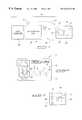
- FIG. 1is a block diagram illustrating a communication system embodying the invention.
- FIG. 2is a front view of an employee badge according to one embodiment of the invention.
- FIG. 3is a front view of a radio frequency identification tag according to another embodiment of the invention.
- FIG. 4is a circuit schematic of a transponder included in the system of FIG. 1 .
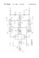
- FIG. 5is a block diagram of an interrogator in accordance with one embodiment of the invention.
- FIG. 6is a circuit schematic of RF circuitry included in the interrogator of FIG. 5 .
- FIG. 7is a circuit schematic of a loop filter included in the RF circuitry of FIG. 6 .
- FIG. 1illustrates a wireless communications system 10 embodying the invention.
- Communications system 10includes a first transponder, including an interrogator 26 , and a host computer 48 in communication with interrogator 26 .
- Communications system 10further includes an electronic communications device 12 , such as the device disclosed in U.S. patent application Ser. No. 08/705,043, filed Aug. 29, 1996.
- wireless communications device 12comprises a wireless identification device such as the Microstamp (TM) integrated circuit available from Micron Communications, Inc., 3176 S. Denver Way, Boise, Id. 83705.
- Interrogator 26communicates with the communications device 12 via an electromagnetic link, such as via an RF link (e.g., at microwave frequencies, in one embodiment).
- TMMicrostamp
- the communications device 12includes a transponder 16 having a receiver 30 and a transmitter 32 (FIG. 4 ). Communications device 12 further includes a power source 18 connected to transponder 16 to supply power to transponder 16 . Communications device 12 further includes at least one antenna connected to transponder 16 for wireless transmission and reception. In the illustrated embodiment, communications device 12 includes at least one antenna 46 connected to transponder 16 for radio frequency transmission by transponder 16 , and at least one receive antenna 44 connected to transponder 16 for radio frequency reception by transponder 16 . In the illustrated embodiment, the transmit antenna 46 is a dipole antenna, and the receive antenna 44 is a loop antenna. In the illustrated embodiment, the transponder 16 is in the form of an integrated circuit. However, in alternative embodiments, all of the circuitry of transponder 16 is not necessarily all included in a single integrated circuit.
- the communications device 12can be included in any appropriate housing or packaging.
- FIG. 2shows but one example of a housing in the form of a card 11 comprising plastic or other suitable material.
- the plastic card 11houses communications device 12 to define an employee identification badge 13 including the communications device 12 .
- the front face of badge 13has visual identification features such as an employee photograph or a fingerprint in addition to identifying text.
- FIG. 3illustrates but one alternative housing supporting the device 12 . More particularly, FIG. 3 illustrates a miniature housing 20 encasing the device 12 to define a tag which can be supported by an object (e.g., hung from an object, affixed to an object, etc.).
- an objecte.g., hung from an object, affixed to an object, etc.
- Communications system 10includes a transmit antenna X 1 , and a receive antenna R 1 connected to interrogator 26 .
- the interrogator 26transmits an interrogation signal or command signal 27 (“forward link”) via the antenna X 1 .
- the communications device 12receives the incoming interrogation signal via its antenna 44 .
- the communications device 12responds by generating and transmitting a responsive signal or reply signal 29 (“return link”).
- the interrogator 26is described in greater detail below.
- the responsive signal 29is encoded with information that uniquely identifies, or labels the particular device 12 that is transmitting, so as to identify any object or person with which communications device 12 is associated.
- FIG. 1illustrates the communications device 12 as being in the housing 20 of FIG. 3 .
- the systemwould operate in a similar manner if the device 12 is provided in a housing such as the housing 10 of FIG. 2, or any other appropriate housing.
- Multiple communications devices 12can be used in the same field of an interrogator 26 (i.e., within communications range of an interrogator 26 ). Similarly, multiple interrogators 26 can be in proximity to one or more of the devices 12 .
- the above described system 10is advantageous over prior art devices that utilize magnetic field effect systems because, with the system 10 , a greater range can be achieved, and more information can be obtained (instead of just an identification number).
- such a system 10can be used, for example, to monitor large warehouse inventories having many unique products needing individual discrimination to determine the presence of particular items within a large lot of tagged products.
- FIG. 4is a high level circuit schematic of the transponder 16 utilized in the devices of FIGS. 1-3.
- the transponder 16is a monolithic integrated circuit. More particularly, in the illustrated embodiment, the integrated circuit 16 comprises a single die, having a size of 209 ⁇ 116 mils 2 , including the receiver 30 , the transmitter 32 , a micro controller or microprocessor 34 , a wake up timer and logic circuit 36 , a clock recovery and data recovery circuit 38 , and a bias voltage and current generator 42 .
- the communications devices 12switch between a “sleep” mode of operation, and higher power modes to conserve energy and extend battery life during periods of time where no interrogation signal 27 is received by devices 12 , using the wake up timer and logic circuitry 36 .
- a spread spectrum processing circuit 40is included in transponder 16 .
- signals transmitted and received by interrogator 26 , and transmitted and received by communications device 12are modulated spread spectrum signals. Spread spectrum modulation is described below.
- the spread spectrum modulation technique employed in the illustrated embodimentrequires a transmission bandwidth that is up to several orders of magnitude greater than the minimum required signal bandwidth.
- spread spectrum modulation techniquesare bandwidth inefficient in single user applications, they are advantageous where there are multiple users, as is the case with the instant radio frequency identification system 24 .
- the spread spectrum modulation technique of the illustrated embodimentis advantageous because the interrogator signal can be distinguished from other signals (e.g., radar, microwave ovens, etc.) operating at the same frequency.
- the spread spectrum signals transmitted by communications device 12 and by interrogator 26are pseudo random and have noise-like properties when compared with the digital command or reply.
- the spreading waveformis controlled by a pseudo-noise or pseudo random number (PN) sequence or code.
- the PN codeis a binary sequence that appears random but can be reproduced in a predetermined manner by the device 12 . More particularly, incoming spread spectrum signals are demodulated by communications device 12 or by interrogator 26 through cross correlation with a version of the pseudo random carrier that is generated by communications device 12 itself or interrogator 26 itself, respectively. Cross correlation with the correct PN sequence unspreads the spread spectrum signal and restores the modulated message in the same narrow band as the original data.
- a pseudo-noise or pseudo random sequenceis a binary sequence with an autocorrelation that resembles, over a period, the autocorrelation of a random binary sequence.
- the autocorrelation of a pseudo-noise sequencealso roughly resembles the autocorrelation of band-limited white noise.
- a pseudo-noise sequencehas many characteristics that are similar to those of random binary sequences. For example, a pseudo-noise sequence has a nearly equal number of zeros and ones, very low correlation between shifted versions of the sequence, and very low cross correlation between any two sequences.
- a pseudo-noise sequenceis usually generated using sequential logic circuits. For example, a pseudo-noise sequence can be generated using a feedback shift register.
- a pseudo-noise sequenceis usually an odd number of chips long.
- one bit of datais represented by a thirty-one chip sequence.
- a zero bit of datais represented by inverting the pseudo-noise sequence.
- the interrogatorsends out a command that is spread around a certain center frequency (e.g, 2.44 GHz).
- a certain center frequencye.g, 2.44 GHz
- the interrogatorswitches to a CW mode (continuous wave mode).
- the continuous wave modethe interrogator does not transmit any information. Instead, the interrogator just transmits 2.44 GHz radiation. In other words, the signal transmitted by the interrogator is not modulated.
- the communications device 12receives the command from the interrogator, the communications device 12 processes the command. If communications device 12 is in a backscatter mode it alternately reflects or does not reflect the signal from the interrogator to send its reply. For example, in the illustrated embodiment, two halves of a dipole antenna are either shorted together or isolated from each other to send a reply.
- the clock for the entire integrated circuit 16is extracted from the incoming message itself by clock recovery and data recovery circuitry 38 .
- This clockis recovered from the incoming message, and used for timing for the micro controller 34 and all the other clock circuitry on the chip, and also for deriving the transmitter carrier or the subcarrier, depending on whether the transmitter is operating in active mode or backscatter mode.
- the clock recovery and data recovery circuit 38In addition to recovering a clock, the clock recovery and data recovery circuit 38 also performs data recovery on valid incoming signals.
- the valid spread spectrum incoming signalis passed through the spread spectrum processing circuit 40 , and the spread spectrum processing circuit 40 extracts the actual ones and zeros of data from the incoming signal. More particularly, the spread spectrum processing circuit 40 takes the chips from the spread spectrum signal, and reduces each thirty-one chip section down to a bit of one or zero, which is passed to the micro controller 34 .
- Micro controller 34includes a serial processor, or I/O facility that receives the bits from the spread spectrum processing circuit 40 .
- the micro controller 34performs further error correction. More particularly, a modified hamming code is employed, where each eight bits of data is accompanied by five check bits used by the micro controller 34 for error correction.
- Micro controller 34further includes a memory, and after performing the data correction, micro controller 34 stores bytes of the data bits in memory. These bytes contain a command sent by the interrogator 26 . The micro controller 34 responds to the command.
- the interrogator 26may send a command requesting that any communications device 12 in the field respond with the device's identification number. Status information is also returned to interrogator 26 from communications device 12 when communications device 12 responds.
- the transmitted replieshave a format similar to the format of incoming messages. More particularly, a reply starts with a preamble (e.g., all zeros in active mode, or alternating double zeros and double ones in backscatter mode), followed by a Barker or start code, followed by actual data.
- a preamblee.g., all zeros in active mode, or alternating double zeros and double ones in backscatter mode
- Barker or start codefollowed by actual data.
- the incoming message and outgoing replypreferably also include a check sum or redundancy code so that integrated circuit 12 or interrogator 26 can confirm receipt of the entire message or reply.
- Interrogator 26provides a communication link between a host computer and transponder 16 .
- Interrogator 26connects to the host computer 48 via an IEEE-1284 enhanced parallel port (EPP).
- EPPenhanced parallel port
- the interrogatorcommunicates with transponder 16 via the RF antennas X 1 and R 1 .
- one embodiment of interrogator 26includes enhanced parallel port (EPP) circuitry 50 , DPSK (differential phase shift keyed) circuitry 52 , and RF (radio frequency) circuitry 54 , as well as a power supply (not shown) and a housing or chassis (not shown).
- EPPenhanced parallel port
- DPSKdifferential phase shift keyed
- RFradio frequency
- the enhanced parallel port circuitry 50 , the DPSK circuitry 52 , and the RF circuitry 54respectively define circuit card assemblies (CCAs).
- the interrogatoruses an IEEE-1284 compatible port in EPP mode to communicate with host computer 48 .
- the EPP circuitry 50provides digital logic required to coordinate sending and receiving a message with transponder 16 .
- RF circuitry 54is configured to transmit the CW signal using antenna X 1 .
- transponder 16selectively backscatters the signal with a DPSK modulated subcarrier providing a microwave communication signal in the described embodiment.
- RF circuitry 54is configured to receive and downconvert signals received from a transponder unit of a remote communications device. Such signals comprise backscatter signals in the described embodiment.
- RF circuitry 54further includes a quadrature downcoverter 84 coupled with amplifier 82 .
- Downconverter 84is configured to receive the communication signal from antenna R 1 and convert the communication signal to the subcarrier having a frequency less than the frequency of the carrier.
- Downconverter 84is configured to convert the received communication signal to an in-phase (I) signal and a quadrature (Q) signal individually having a subcarrier frequency, such as 600 kHz.
- Mixers 55 , 57are configured to mix the output of power divider 53 with the output of power divider 59 . Mixing the outputs of power dividers 53 , 59 provides the quadrature downconverting operations and generates the subcarrier signal.
- mixer 55is configured to output an in-phase (I) signal.
- Mixer 57is configured to output a quadrature (Q) signal.
- signals I, Qhave a frequency of approximately 600 kHz responsive to the modulation frequency within the remote communication device 12 .
- Filters 63 , 65are preferably configured to filter the respective in-phase and quadrature signals about the subcarrier frequency. More specifically, filters 63 , 65 are configured to band limit the in-phase signal and quadrature signal. Filters 63 , 65 comprise band pass filters configured to filter the in-phase signal and the quadrature signal about the subcarrier frequency. Such removes direct path energy and higher frequency products (e.g., X 2 components) resulting from the mixing of plural 2.44 GHz signals.
- filters 63 , 65are preferably configured to filter the respective in-phase and quadrature signals about the subcarrier frequency. More specifically, filters 63 , 65 are configured to band limit the in-phase signal and quadrature signal. Filters 63 , 65 comprise band pass filters configured to filter the in-phase signal and the quadrature signal about the subcarrier frequency. Such removes direct path energy and higher frequency products (e.g., X 2 components) resulting from the mixing of plural 2.44 GHz signals.
- interrogator 26is typically simultaneously transmitting the CW signal using antenna X 1 during reception of communication signals using antenna R 1 .
- Communications via X 1 and R 1typically occur at approximately the same frequencies.
- a certain amount of signalmay bleed over from the transmitted signals.
- Other energymay be reflected from static objects present in the communication environment.
- low frequency modulationsmay be present responsive to moving objects within the communication environment.
- DC signals and low frequency signalsmay be present within signals I, Q.
- Filters 63 , 65remove noise and other undesired frequencies from signals I, Q.
- the filtered in-phase signal and quadrature signalare applied to respective amplifiers 67 , 69 .
- Exemplary amplifiers 67 , 69have designation CLC425 available from National Semiconductor Corporation.
- plural automatic gain control (AGC) amplifiersare coupled with amplifiers 67 , 69 .
- AGC amplifiersare cascaded within the respective in-phase and quadrature signal lines or channels.
- Cascaded amplifiers 71 , 73are coupled with amplifier 67 and configured to receive the in-phase signal.
- Cascaded AGC amplifiers 75 , 77are coupled with amplifier 69 and are configured to receive the quadrature signal.
- the amplitudes of the I, Q signalsare set using the gain controls 45 , 47 .
- the depicted gain controls 45 , 47are configured to adjust the gain of the in-phase signal and the quadrature signal.
- Gain controls 45 , 47operate to maintain the receive operations of interrogator 26 within a linear region in a preferred embodiment.
- Automatic gain controlsare preferably utilized to provide a variable amount of gain so the in-phase and quadrature signals are amplified without compressing or saturating components along the receive paths.
- Gain controls 45 , 47can control the levels of signals I, Q containing the desired information following removal of the direct path energy.
- the gain controlsare preferably configured to maintain the amplitude of the in-phase signal relative to the amplitude of the quadrature signal while the gain of the respective signals is increased. It is desired to maintain the relative amplitudes of the in-phase and quadrature signals with reference to one another for downstream signal processing.
- a detector or controller 49is coupled with gain controls 45 , 47 of the in-phase signal path and the quadrature signal path in the illustrated embodiment.
- controller 49is configured to monitor the I and Q channel outputs of quadrature downconverter 84 and control the gain of gain controls 45 , 47 such that the highest or peak levels of either the I or Q signals are maintained at a constant level.
- the AGC circuitryis preferably configured to maintain constant level signals for application to downstream modulation circuitry regardless of the input level from receive antenna R 1 . Such tends to maximize performance within downstream demodulation processing steps and minimize effects upon the I and Q channels prior to the demodulation.
- the depicted controller 49comprises a loop filter 79 and plural diodes 81 , 83 .
- Loop filter 79 and diodes 81 , 83are utilized in the described embodiment to control the gain adjustment of the in-phase and quadrature signals through respective gain controls 45 , 47 .
- Diode 81couples the in-phase signal path with a node 87 .
- Diode 83couples the quadrature signal path with node 87 .
- Loop filter 79is coupled intermediate plural nodes 85 , 87 .
- Loop filter 79is designed to apply a common control signal to AGC amplifiers 71 , 73 , 75 , 77 of gain controls 45 , 47 in the described embodiment.
- controller 49is configured to output a control signal to AGC amplifiers 71 , 73 , 75 , 77 of gain controls 45 , 47 to control adjustment of the gain of the in-phase signal and the quadrature signal in a preferred embodiment of the invention.
- the common control signalis utilized to maintain the relationship of the amplitude of the in-phase signal relative to the amplitude of the quadrature signal. Such enables utilization of quadrature combination techniques to reconstruct the original signal.
- loop filter 79comprises a feedback loop consisting of an operational amplifier 89 and discrete devices coupled intermediate nodes 85 , 87 .
- Node 87is coupled with diodes 81 , 83 of the respective in-phase and quadrature signal paths.
- Loop filter 79provides feedback control of in-phase and quadrature gain controls 45 , 47 .
- Diodes 81 , 83provide an OR function to utilize the individual I or Q signal having the higher amplitude to control automatic gain control amplifiers 71 , 73 , 75 , 77 .
- Diodes 81 , 83are provided to detect peak levels within the in-phase and quadrature signal paths. Diodes 81 , 83 are configured to detect the signal having the higher amplitude.
- controller 49Responsive to the detected peak voltages, controller 49 outputs control signals via node 85 to the respective in-phase and quadrature gain controls.
- the described RF circuitry 54maintains the amplitude relationship of the I and Q signals for subsequent processing.
- the I and Q signalswhich contain the DPSK modulated subcarrier, are passed to DPSK circuitry 52 for demodulation.
- DPSK circuitry 52receives signals I and Q from RF circuitry 54 .
- the I and Q signalscontain the DPSK modulated subcarrier.
- the DPSK circuitry 52includes anti-aliasing filters 56 and 58 filtering the I and Q signals, respectively, and analog to digital (A/D) converters 60 , 62 respectively coupled to filters 56 , 58 and respectively converting the filtered signals from analog to digital signals.
- DPSK circuitry 52further includes a combiner 64 , coupled to the A/D converters 60 and 62 , combining the digital signals.
- DPSK circuitry 52further includes a FIR matched filter 66 , coupled to the combiner 64 , which filters the combined signals.
- the DPSK circuitry 52further includes delay circuitry 68 and multiplier circuitry 70 coupled to the FIR matched filter 66 for delaying the signal and multiplying the signal with the delayed signal to remove the subcarrier.
- DPSK circuitry 52further includes low pass filter circuitry 72 , coupled to the multiplier 70 , filtering the output of the multiplier 70 to remove the X 2 component.
- the DPSK circuitry 52further includes a bit synchronizer 74 coupled to the filter 72 for regeneration of the data clock.
- the DPSK circuitry 52further includes lock detect circuitry 76 coupled to the low pass filter 72 and generating a lock detect signal. The data, clock, and lock detect signals are sent to the EPP circuitry 50 for subsequent processing.
Landscapes
- Engineering & Computer Science (AREA)
- Artificial Intelligence (AREA)
- Computer Vision & Pattern Recognition (AREA)
- Physics & Mathematics (AREA)
- General Physics & Mathematics (AREA)
- Theoretical Computer Science (AREA)
- Power Engineering (AREA)
- Near-Field Transmission Systems (AREA)
Abstract
Description
Claims (61)
Priority Applications (3)
| Application Number | Priority Date | Filing Date | Title |
|---|---|---|---|
| US09/066,738US6324211B1 (en) | 1998-04-24 | 1998-04-24 | Interrogators communication systems communication methods and methods of processing a communication signal |
| PCT/US1999/008176WO1999056233A1 (en) | 1998-04-24 | 1999-04-14 | Interrogators, communication systems, communication methods, and methods of processing a communication signal |
| AU34938/99AAU3493899A (en) | 1998-04-24 | 1999-04-14 | Interrogators, communication systems, communication methods, and methods of processing a communication signal |
Applications Claiming Priority (1)
| Application Number | Priority Date | Filing Date | Title |
|---|---|---|---|
| US09/066,738US6324211B1 (en) | 1998-04-24 | 1998-04-24 | Interrogators communication systems communication methods and methods of processing a communication signal |
Publications (1)
| Publication Number | Publication Date |
|---|---|
| US6324211B1true US6324211B1 (en) | 2001-11-27 |
Family
ID=22071375
Family Applications (1)
| Application Number | Title | Priority Date | Filing Date |
|---|---|---|---|
| US09/066,738Expired - LifetimeUS6324211B1 (en) | 1998-04-24 | 1998-04-24 | Interrogators communication systems communication methods and methods of processing a communication signal |
Country Status (3)
| Country | Link |
|---|---|
| US (1) | US6324211B1 (en) |
| AU (1) | AU3493899A (en) |
| WO (1) | WO1999056233A1 (en) |
Cited By (46)
| Publication number | Priority date | Publication date | Assignee | Title |
|---|---|---|---|---|
| US6445743B1 (en)* | 1998-02-17 | 2002-09-03 | Koninklijke Philips Electronics N.V. | Transmitting-receiving station having impedance-matched receiving means for transponder answer signals |
| US6454708B1 (en)* | 1999-04-15 | 2002-09-24 | Nexan Limited | Portable remote patient telemonitoring system using a memory card or smart card |
| US6631271B1 (en)* | 2000-08-29 | 2003-10-07 | James D. Logan | Rules based methods and apparatus |
| US20030225987A1 (en)* | 2002-05-28 | 2003-12-04 | Micron Technology, Inc. | Software command sequence for optimized power consumption |
| US20040113747A1 (en)* | 2002-12-17 | 2004-06-17 | M/A-Com, Inc. | Apparatus, methods and articles of manufacture for a multi-band switch |
| US20040141470A1 (en)* | 2002-12-17 | 2004-07-22 | M/A Com, Inc. | Apparatus, methods and articles of manufacture for a multi-band switch |
| US6856794B1 (en)* | 2000-07-27 | 2005-02-15 | Sirf Technology, Inc. | Monolithic GPS RF front end integrated circuit |
| US20050054290A1 (en)* | 2000-08-29 | 2005-03-10 | Logan James D. | Rules based methods and apparatus for generating notification messages based on the proximity of electronic devices to one another |
| US20050207364A1 (en)* | 1998-02-19 | 2005-09-22 | Wood Clifton W Jr | Method of addressing messages and communications system |
| US20060290438A1 (en)* | 2004-02-27 | 2006-12-28 | Micron Technology, Inc. | Microstrip line dielectric overlay |
| WO2007052973A1 (en)* | 2005-11-03 | 2007-05-10 | Lg Innotek Co., Ltd | Rfid reader and rfid system |
| US20070208232A1 (en)* | 2006-03-03 | 2007-09-06 | Physiowave Inc. | Physiologic monitoring initialization systems and methods |
| US20070208233A1 (en)* | 2006-03-03 | 2007-09-06 | Physiowave Inc. | Integrated physiologic monitoring systems and methods |
| US20080180221A1 (en)* | 2007-01-30 | 2008-07-31 | Micron Technology, Inc. | Systems and methods for RFID tag arbitration |
| US20080297324A1 (en)* | 2007-05-30 | 2008-12-04 | Micron Technology, Inc. | Methods and systems of receiving data payload of rfid tags |
| USRE40686E1 (en) | 1998-02-19 | 2009-03-31 | Keystone Technology Solutions, Llc | Method of addressing messages and communications system |
| US7616705B1 (en) | 2000-07-27 | 2009-11-10 | Sirf Technology Holdings, Inc. | Monolithic GPS RF front end integrated circuit |
| US7668588B2 (en) | 2006-03-03 | 2010-02-23 | PhysioWave, Inc. | Dual-mode physiologic monitoring systems and methods |
| US7735101B2 (en) | 2006-03-28 | 2010-06-08 | Cisco Technology, Inc. | System allowing users to embed comments at specific points in time into media presentation |
| USRE41531E1 (en) | 1998-02-19 | 2010-08-17 | Round Rock Research, Llc | Communications systems for radio frequency identification (RFID) |
| USRE42344E1 (en) | 1998-02-19 | 2011-05-10 | Round Rock Research, Llc | Method and apparatus to manage RFID tags |
| US7959769B2 (en) | 2004-12-08 | 2011-06-14 | Infinite Power Solutions, Inc. | Deposition of LiCoO2 |
| US7993773B2 (en) | 2002-08-09 | 2011-08-09 | Infinite Power Solutions, Inc. | Electrochemical apparatus with barrier layer protected substrate |
| US8021778B2 (en) | 2002-08-09 | 2011-09-20 | Infinite Power Solutions, Inc. | Electrochemical apparatus with barrier layer protected substrate |
| US8062708B2 (en) | 2006-09-29 | 2011-11-22 | Infinite Power Solutions, Inc. | Masking of and material constraint for depositing battery layers on flexible substrates |
| US20110309204A1 (en)* | 2009-03-02 | 2011-12-22 | Siemens Aktiengesellschaft | Device for detecting the occupied state and the free state of a track section as well as method for operating such a device |
| US20120077518A1 (en)* | 2000-08-29 | 2012-03-29 | Logan James D | Communication and control system using location aware devices for producing notification messages operating under rule-based control |
| USRE43382E1 (en) | 1998-02-19 | 2012-05-15 | Round Rock Research, Llc | Method of addressing messages and communications systems |
| US8197781B2 (en) | 2006-11-07 | 2012-06-12 | Infinite Power Solutions, Inc. | Sputtering target of Li3PO4 and method for producing same |
| US8236443B2 (en) | 2002-08-09 | 2012-08-07 | Infinite Power Solutions, Inc. | Metal film encapsulation |
| US8260203B2 (en) | 2008-09-12 | 2012-09-04 | Infinite Power Solutions, Inc. | Energy device with integral conductive surface for data communication via electromagnetic energy and method thereof |
| US8268488B2 (en) | 2007-12-21 | 2012-09-18 | Infinite Power Solutions, Inc. | Thin film electrolyte for thin film batteries |
| US8350519B2 (en) | 2008-04-02 | 2013-01-08 | Infinite Power Solutions, Inc | Passive over/under voltage control and protection for energy storage devices associated with energy harvesting |
| US8394522B2 (en) | 2002-08-09 | 2013-03-12 | Infinite Power Solutions, Inc. | Robust metal film encapsulation |
| US8404376B2 (en) | 2002-08-09 | 2013-03-26 | Infinite Power Solutions, Inc. | Metal film encapsulation |
| US8431264B2 (en) | 2002-08-09 | 2013-04-30 | Infinite Power Solutions, Inc. | Hybrid thin-film battery |
| US8445130B2 (en) | 2002-08-09 | 2013-05-21 | Infinite Power Solutions, Inc. | Hybrid thin-film battery |
| US8508193B2 (en) | 2008-10-08 | 2013-08-13 | Infinite Power Solutions, Inc. | Environmentally-powered wireless sensor module |
| US8518581B2 (en) | 2008-01-11 | 2013-08-27 | Inifinite Power Solutions, Inc. | Thin film encapsulation for thin film batteries and other devices |
| US8599572B2 (en) | 2009-09-01 | 2013-12-03 | Infinite Power Solutions, Inc. | Printed circuit board with integrated thin film battery |
| US8636876B2 (en) | 2004-12-08 | 2014-01-28 | R. Ernest Demaray | Deposition of LiCoO2 |
| US8728285B2 (en) | 2003-05-23 | 2014-05-20 | Demaray, Llc | Transparent conductive oxides |
| US8906523B2 (en) | 2008-08-11 | 2014-12-09 | Infinite Power Solutions, Inc. | Energy device with integral collector surface for electromagnetic energy harvesting and method thereof |
| US9334557B2 (en) | 2007-12-21 | 2016-05-10 | Sapurast Research Llc | Method for sputter targets for electrolyte films |
| US9634296B2 (en) | 2002-08-09 | 2017-04-25 | Sapurast Research Llc | Thin film battery on an integrated circuit or circuit board and method thereof |
| US10680277B2 (en) | 2010-06-07 | 2020-06-09 | Sapurast Research Llc | Rechargeable, high-density electrochemical device |
Families Citing this family (1)
| Publication number | Priority date | Publication date | Assignee | Title |
|---|---|---|---|---|
| US11678112B2 (en) | 2020-04-30 | 2023-06-13 | Massachusetts Institute Of Technology | Underwater transducer for wide-band communication |
Citations (9)
| Publication number | Priority date | Publication date | Assignee | Title |
|---|---|---|---|---|
| US4075632A (en) | 1974-08-27 | 1978-02-21 | The United States Of America As Represented By The United States Department Of Energy | Interrogation, and detection system |
| US4504786A (en) | 1982-06-14 | 1985-03-12 | Slaughter Grimes G | Signal detector |
| US4926182A (en) | 1986-05-30 | 1990-05-15 | Sharp Kabushiki Kaisha | Microwave data transmission apparatus |
| EP0501740A2 (en) | 1991-02-25 | 1992-09-02 | Rockwell International Corporation | Phase and gain error control system for use in an I/Q direct conversion receiver |
| WO1997008842A1 (en) | 1995-08-30 | 1997-03-06 | Pacific Communication Sciences, Inc. | Near direct conversion receiver and method for equalizing amplitude and phase therein |
| US5617060A (en) | 1994-04-28 | 1997-04-01 | Qualcomm Incorporated | Method and apparatus for automatic gain control and DC offset cancellation in quadrature receiver |
| US5621412A (en) | 1994-04-26 | 1997-04-15 | Texas Instruments Incorporated | Multi-stage transponder wake-up, method and structure |
| US5640424A (en) | 1995-05-16 | 1997-06-17 | Interstate Electronics Corporation | Direct downconverter circuit for demodulator in digital data transmission system |
| US5649296A (en) | 1995-06-19 | 1997-07-15 | Lucent Technologies Inc. | Full duplex modulated backscatter system |
- 1998
- 1998-04-24USUS09/066,738patent/US6324211B1/ennot_activeExpired - Lifetime
- 1999
- 1999-04-14AUAU34938/99Apatent/AU3493899A/ennot_activeAbandoned
- 1999-04-14WOPCT/US1999/008176patent/WO1999056233A1/enactiveApplication Filing
Patent Citations (11)
| Publication number | Priority date | Publication date | Assignee | Title |
|---|---|---|---|---|
| US4075632A (en) | 1974-08-27 | 1978-02-21 | The United States Of America As Represented By The United States Department Of Energy | Interrogation, and detection system |
| US4504786A (en) | 1982-06-14 | 1985-03-12 | Slaughter Grimes G | Signal detector |
| US4926182A (en) | 1986-05-30 | 1990-05-15 | Sharp Kabushiki Kaisha | Microwave data transmission apparatus |
| EP0501740A2 (en) | 1991-02-25 | 1992-09-02 | Rockwell International Corporation | Phase and gain error control system for use in an I/Q direct conversion receiver |
| US5249203A (en) | 1991-02-25 | 1993-09-28 | Rockwell International Corporation | Phase and gain error control system for use in an i/q direct conversion receiver |
| US5621412A (en) | 1994-04-26 | 1997-04-15 | Texas Instruments Incorporated | Multi-stage transponder wake-up, method and structure |
| US5617060A (en) | 1994-04-28 | 1997-04-01 | Qualcomm Incorporated | Method and apparatus for automatic gain control and DC offset cancellation in quadrature receiver |
| US5640424A (en) | 1995-05-16 | 1997-06-17 | Interstate Electronics Corporation | Direct downconverter circuit for demodulator in digital data transmission system |
| US5649296A (en) | 1995-06-19 | 1997-07-15 | Lucent Technologies Inc. | Full duplex modulated backscatter system |
| WO1997008842A1 (en) | 1995-08-30 | 1997-03-06 | Pacific Communication Sciences, Inc. | Near direct conversion receiver and method for equalizing amplitude and phase therein |
| US5828955A (en) | 1995-08-30 | 1998-10-27 | Rockwell Semiconductor Systems, Inc. | Near direct conversion receiver and method for equalizing amplitude and phase therein |
Non-Patent Citations (3)
| Title |
|---|
| P. 827 of New IEEE Standard Dictionary of Electrical & Electronic Terms, 1993. |
| U.S. application No. 08/705,043, O'Toole et al., filed Aug. 29, 1996. |
| U.S. application Ser. No. 08/705,043, O'Toole et al., filed Aug. 29, 1992. |
Cited By (92)
| Publication number | Priority date | Publication date | Assignee | Title |
|---|---|---|---|---|
| US6445743B1 (en)* | 1998-02-17 | 2002-09-03 | Koninklijke Philips Electronics N.V. | Transmitting-receiving station having impedance-matched receiving means for transponder answer signals |
| US7639638B2 (en) | 1998-02-19 | 2009-12-29 | Keystone Technology Solutions, Llc | Method and apparatus for an arbitration scheme for radio frequency identification devices |
| USRE43445E1 (en) | 1998-02-19 | 2012-06-05 | Round Rock Research, Llc | Method and apparatus to manage RFID tags |
| USRE42254E1 (en) | 1998-02-19 | 2011-03-29 | Round Rock Research, Llc | Method of addressing messages and communications system |
| US9014077B2 (en) | 1998-02-19 | 2015-04-21 | Round Rock Research, Llc | Methods and apparatus for conducting financial transactions |
| USRE42344E1 (en) | 1998-02-19 | 2011-05-10 | Round Rock Research, Llc | Method and apparatus to manage RFID tags |
| USRE41530E1 (en) | 1998-02-19 | 2010-08-17 | Round Rock Research, Llc | Method and apparatus to select radio frequency identification devices in accordance with an arbitration scheme |
| USRE41531E1 (en) | 1998-02-19 | 2010-08-17 | Round Rock Research, Llc | Communications systems for radio frequency identification (RFID) |
| US20050207364A1 (en)* | 1998-02-19 | 2005-09-22 | Wood Clifton W Jr | Method of addressing messages and communications system |
| USRE41471E1 (en) | 1998-02-19 | 2010-08-03 | Round Rock Research, Llc | Method of Addressing Messages and Communications System |
| US20060056325A1 (en)* | 1998-02-19 | 2006-03-16 | Wood Clifton W Jr | Method of addressing messages and communications system |
| US20060209781A1 (en)* | 1998-02-19 | 2006-09-21 | Micron Technology, Inc. | Method of addressing messages and communications system |
| US8638709B2 (en) | 1998-02-19 | 2014-01-28 | Round Rock Research, Llc | Methods and apparatus for conducting financial transactions |
| US8634338B2 (en) | 1998-02-19 | 2014-01-21 | Round Rock Research, Llc | Methods and apparatus for conducting financial transactions |
| US7760677B2 (en) | 1998-02-19 | 2010-07-20 | Keystone Technology Solutions, Llc | Method of addressing messages and communications system |
| USRE44411E1 (en) | 1998-02-19 | 2013-08-06 | Round Rock Research, Llc | Method of addressing messages, method of establishing wireless communications and communications system |
| US8488581B2 (en) | 1998-02-19 | 2013-07-16 | Round Rock Research, Llc | Methods and apparatus for conducting financial transactions |
| USRE42599E1 (en) | 1998-02-19 | 2011-08-09 | Round Rock Research, Llc | Method of addressing messages and communications system |
| US20080007412A1 (en)* | 1998-02-19 | 2008-01-10 | Wood Clifton W Jr | Method of Addressing Messages and Communications System |
| US20080042806A1 (en)* | 1998-02-19 | 2008-02-21 | Wood Clifton W Jr | Method of Addressing Messages and Communications System |
| USRE41352E1 (en) | 1998-02-19 | 2010-05-25 | Keystone Technology Solutions, Llc | Method of addressing messages and communications |
| US7672260B2 (en) | 1998-02-19 | 2010-03-02 | Keystone Technology Solutions, Llc | Method of addressing messages and communications system |
| USRE43382E1 (en) | 1998-02-19 | 2012-05-15 | Round Rock Research, Llc | Method of addressing messages and communications systems |
| US8040829B2 (en) | 1998-02-19 | 2011-10-18 | Round Rock Research, Llc | Method of addressing messages and communications system |
| US20090322491A1 (en)* | 1998-02-19 | 2009-12-31 | Keystone Technology Solutions, Llc | Method of Addressing Messages and Communications System |
| USRE43254E1 (en) | 1998-02-19 | 2012-03-20 | Round Rock Research, Llc | Method of addressing messages and communications systems |
| USRE43020E1 (en) | 1998-02-19 | 2011-12-13 | Round Rock Research, Llc | Method of addressing messages, method of establishing wireless communications, and communications system |
| USRE40686E1 (en) | 1998-02-19 | 2009-03-31 | Keystone Technology Solutions, Llc | Method of addressing messages and communications system |
| USRE42900E1 (en) | 1998-02-19 | 2011-11-08 | Round Rock Research, Llc | Method of addressing messages and communications systems |
| US7936706B2 (en) | 1998-02-19 | 2011-05-03 | Round Rock Research, Llc | Method of addressing messages and communications system |
| US6454708B1 (en)* | 1999-04-15 | 2002-09-24 | Nexan Limited | Portable remote patient telemonitoring system using a memory card or smart card |
| US7616705B1 (en) | 2000-07-27 | 2009-11-10 | Sirf Technology Holdings, Inc. | Monolithic GPS RF front end integrated circuit |
| US7369830B2 (en) | 2000-07-27 | 2008-05-06 | Sirf Technology, Inc. | Monolithic GPS RF front end integrated circuit |
| US6856794B1 (en)* | 2000-07-27 | 2005-02-15 | Sirf Technology, Inc. | Monolithic GPS RF front end integrated circuit |
| US20120077518A1 (en)* | 2000-08-29 | 2012-03-29 | Logan James D | Communication and control system using location aware devices for producing notification messages operating under rule-based control |
| US6631271B1 (en)* | 2000-08-29 | 2003-10-07 | James D. Logan | Rules based methods and apparatus |
| US6996402B2 (en)* | 2000-08-29 | 2006-02-07 | Logan James D | Rules based methods and apparatus for generating notification messages based on the proximity of electronic devices to one another |
| US20050054290A1 (en)* | 2000-08-29 | 2005-03-10 | Logan James D. | Rules based methods and apparatus for generating notification messages based on the proximity of electronic devices to one another |
| US8938256B2 (en)* | 2000-08-29 | 2015-01-20 | Intel Corporation | Communication and control system using location aware devices for producing notification messages operating under rule-based control |
| US7305514B2 (en) | 2002-05-28 | 2007-12-04 | Micron Technology, Inc. | Command sequence for optimized power consumption |
| US7251711B2 (en) | 2002-05-28 | 2007-07-31 | Micron Technology, Inc. | Apparatus and methods having a command sequence |
| US20030225987A1 (en)* | 2002-05-28 | 2003-12-04 | Micron Technology, Inc. | Software command sequence for optimized power consumption |
| US8404376B2 (en) | 2002-08-09 | 2013-03-26 | Infinite Power Solutions, Inc. | Metal film encapsulation |
| US8431264B2 (en) | 2002-08-09 | 2013-04-30 | Infinite Power Solutions, Inc. | Hybrid thin-film battery |
| US8535396B2 (en) | 2002-08-09 | 2013-09-17 | Infinite Power Solutions, Inc. | Electrochemical apparatus with barrier layer protected substrate |
| US9634296B2 (en) | 2002-08-09 | 2017-04-25 | Sapurast Research Llc | Thin film battery on an integrated circuit or circuit board and method thereof |
| US7993773B2 (en) | 2002-08-09 | 2011-08-09 | Infinite Power Solutions, Inc. | Electrochemical apparatus with barrier layer protected substrate |
| US8445130B2 (en) | 2002-08-09 | 2013-05-21 | Infinite Power Solutions, Inc. | Hybrid thin-film battery |
| US8021778B2 (en) | 2002-08-09 | 2011-09-20 | Infinite Power Solutions, Inc. | Electrochemical apparatus with barrier layer protected substrate |
| US8236443B2 (en) | 2002-08-09 | 2012-08-07 | Infinite Power Solutions, Inc. | Metal film encapsulation |
| US9793523B2 (en) | 2002-08-09 | 2017-10-17 | Sapurast Research Llc | Electrochemical apparatus with barrier layer protected substrate |
| US8394522B2 (en) | 2002-08-09 | 2013-03-12 | Infinite Power Solutions, Inc. | Robust metal film encapsulation |
| US20040141470A1 (en)* | 2002-12-17 | 2004-07-22 | M/A Com, Inc. | Apparatus, methods and articles of manufacture for a multi-band switch |
| US7515882B2 (en)* | 2002-12-17 | 2009-04-07 | Kelcourse Mark F | Apparatus, methods and articles of manufacture for a multi-band switch |
| US7869770B2 (en) | 2002-12-17 | 2011-01-11 | M/A-Com Technology Solutions Holdings, Inc. | Apparatus, methods and articles of manufacture for a multi-band switch |
| US20040113747A1 (en)* | 2002-12-17 | 2004-06-17 | M/A-Com, Inc. | Apparatus, methods and articles of manufacture for a multi-band switch |
| US8728285B2 (en) | 2003-05-23 | 2014-05-20 | Demaray, Llc | Transparent conductive oxides |
| US7432774B2 (en) | 2004-02-27 | 2008-10-07 | Micron Technology, Inc. | Microstrip line dielectric overlay |
| US20090025204A1 (en)* | 2004-02-27 | 2009-01-29 | Micron Technology, Inc. | Microstrip line dielectric overlay |
| US20060290438A1 (en)* | 2004-02-27 | 2006-12-28 | Micron Technology, Inc. | Microstrip line dielectric overlay |
| US9214713B2 (en) | 2004-02-27 | 2015-12-15 | Micron Technology, Inc. | Method of fabricating a microstrip line dielectric overlay |
| US7436267B2 (en) | 2004-02-27 | 2008-10-14 | Micron Technology, Inc. | Microstrip line dielectric overlay |
| US7959769B2 (en) | 2004-12-08 | 2011-06-14 | Infinite Power Solutions, Inc. | Deposition of LiCoO2 |
| US8636876B2 (en) | 2004-12-08 | 2014-01-28 | R. Ernest Demaray | Deposition of LiCoO2 |
| WO2007052973A1 (en)* | 2005-11-03 | 2007-05-10 | Lg Innotek Co., Ltd | Rfid reader and rfid system |
| US8154386B2 (en) | 2005-11-03 | 2012-04-10 | Lg Innotek Co., Ltd. | RFID reader and RFID system |
| US20080278329A1 (en)* | 2005-11-03 | 2008-11-13 | Lg Innotek Co., Ltd | Rfid Reader and Rfid System |
| US20070208232A1 (en)* | 2006-03-03 | 2007-09-06 | Physiowave Inc. | Physiologic monitoring initialization systems and methods |
| US7668588B2 (en) | 2006-03-03 | 2010-02-23 | PhysioWave, Inc. | Dual-mode physiologic monitoring systems and methods |
| US20070208233A1 (en)* | 2006-03-03 | 2007-09-06 | Physiowave Inc. | Integrated physiologic monitoring systems and methods |
| US8200320B2 (en) | 2006-03-03 | 2012-06-12 | PhysioWave, Inc. | Integrated physiologic monitoring systems and methods |
| US7735101B2 (en) | 2006-03-28 | 2010-06-08 | Cisco Technology, Inc. | System allowing users to embed comments at specific points in time into media presentation |
| US8332886B2 (en) | 2006-03-28 | 2012-12-11 | Michael Lanza | System allowing users to embed comments at specific points in time into media presentation |
| US8062708B2 (en) | 2006-09-29 | 2011-11-22 | Infinite Power Solutions, Inc. | Masking of and material constraint for depositing battery layers on flexible substrates |
| US8197781B2 (en) | 2006-11-07 | 2012-06-12 | Infinite Power Solutions, Inc. | Sputtering target of Li3PO4 and method for producing same |
| US20080180221A1 (en)* | 2007-01-30 | 2008-07-31 | Micron Technology, Inc. | Systems and methods for RFID tag arbitration |
| US7973644B2 (en) | 2007-01-30 | 2011-07-05 | Round Rock Research, Llc | Systems and methods for RFID tag arbitration where RFID tags generate multiple random numbers for different arbitration sessions |
| US8207856B2 (en) | 2007-01-30 | 2012-06-26 | Round Rock Research, Llc | Systems and methods for RFID tag arbitration where RFID tags generate multiple random numbers for different arbitration sessions |
| US20080297324A1 (en)* | 2007-05-30 | 2008-12-04 | Micron Technology, Inc. | Methods and systems of receiving data payload of rfid tags |
| US8134452B2 (en) | 2007-05-30 | 2012-03-13 | Round Rock Research, Llc | Methods and systems of receiving data payload of RFID tags |
| US9334557B2 (en) | 2007-12-21 | 2016-05-10 | Sapurast Research Llc | Method for sputter targets for electrolyte films |
| US8268488B2 (en) | 2007-12-21 | 2012-09-18 | Infinite Power Solutions, Inc. | Thin film electrolyte for thin film batteries |
| US8518581B2 (en) | 2008-01-11 | 2013-08-27 | Inifinite Power Solutions, Inc. | Thin film encapsulation for thin film batteries and other devices |
| US9786873B2 (en) | 2008-01-11 | 2017-10-10 | Sapurast Research Llc | Thin film encapsulation for thin film batteries and other devices |
| US8350519B2 (en) | 2008-04-02 | 2013-01-08 | Infinite Power Solutions, Inc | Passive over/under voltage control and protection for energy storage devices associated with energy harvesting |
| US8906523B2 (en) | 2008-08-11 | 2014-12-09 | Infinite Power Solutions, Inc. | Energy device with integral collector surface for electromagnetic energy harvesting and method thereof |
| US8260203B2 (en) | 2008-09-12 | 2012-09-04 | Infinite Power Solutions, Inc. | Energy device with integral conductive surface for data communication via electromagnetic energy and method thereof |
| US8508193B2 (en) | 2008-10-08 | 2013-08-13 | Infinite Power Solutions, Inc. | Environmentally-powered wireless sensor module |
| US20110309204A1 (en)* | 2009-03-02 | 2011-12-22 | Siemens Aktiengesellschaft | Device for detecting the occupied state and the free state of a track section as well as method for operating such a device |
| US9532453B2 (en) | 2009-09-01 | 2016-12-27 | Sapurast Research Llc | Printed circuit board with integrated thin film battery |
| US8599572B2 (en) | 2009-09-01 | 2013-12-03 | Infinite Power Solutions, Inc. | Printed circuit board with integrated thin film battery |
| US10680277B2 (en) | 2010-06-07 | 2020-06-09 | Sapurast Research Llc | Rechargeable, high-density electrochemical device |
Also Published As
| Publication number | Publication date |
|---|---|
| WO1999056233A1 (en) | 1999-11-04 |
| AU3493899A (en) | 1999-11-16 |
Similar Documents
| Publication | Publication Date | Title |
|---|---|---|
| US6324211B1 (en) | Interrogators communication systems communication methods and methods of processing a communication signal | |
| US6075973A (en) | Method of communications in a backscatter system, interrogator, and backscatter communications system | |
| US6169474B1 (en) | Method of communications in a backscatter system, interrogator, and backscatter communications system | |
| US8855169B2 (en) | Methods and apparatus for RFID tag communications | |
| US6289209B1 (en) | Wireless communication system, radio frequency communications system, wireless communications method, radio frequency communications method | |
| USRE43242E1 (en) | Communication system, interrogators and communication methods | |
| US6356764B1 (en) | Wireless communication systems, interrogators and methods of communicating within a wireless communication system | |
| US7982586B2 (en) | Wireless communication systems, interrogators and methods of communicating within a wireless communication system | |
| US7091828B2 (en) | Interrogators, methods of operating a coherent interrogator, backscatter communication methods, interrogation methods, and signal processing methods | |
| US5539775A (en) | Modulated spread spectrum in RF identification systems method | |
| EP0750201B1 (en) | Full duplex modulated backscatter system | |
| EP0915573A2 (en) | Direct sequence spread spectrum modulated uplink for modulated backscatter systems | |
| JP2003234672A (en) | Backscatter electronic shelf label system by wide spread spectrum modulation system | |
| WO1999008402A1 (en) | Wireless communication system including a plurality of selectable antennas and wireless communications method |
Legal Events
| Date | Code | Title | Description |
|---|---|---|---|
| AS | Assignment | Owner name:MICRON COMMUNICATIONS, INC., IDAHO Free format text:ASSIGNMENT OF ASSIGNORS INTEREST;ASSIGNORS:OVARD, DAVID K.;GREEFF, ROY;REEL/FRAME:009378/0430 Effective date:19980702 | |
| AS | Assignment | Owner name:MICRON TECHNOLOGY, INC., IDAHO Free format text:MERGER;ASSIGNOR:MICRON COMMUNICATIONS, INC.;REEL/FRAME:010381/0184 Effective date:19990901 | |
| STCF | Information on status: patent grant | Free format text:PATENTED CASE | |
| FEPP | Fee payment procedure | Free format text:PAYOR NUMBER ASSIGNED (ORIGINAL EVENT CODE: ASPN); ENTITY STATUS OF PATENT OWNER: LARGE ENTITY | |
| CC | Certificate of correction | ||
| FPAY | Fee payment | Year of fee payment:4 | |
| AS | Assignment | Owner name:KEYSTONE TECHNOLOGY SOLUTIONS, LLC, IDAHO Free format text:ASSIGNMENT OF ASSIGNORS INTEREST;ASSIGNOR:MICRON TECHNOLOGY, INC.;REEL/FRAME:019825/0542 Effective date:20070628 Owner name:KEYSTONE TECHNOLOGY SOLUTIONS, LLC,IDAHO Free format text:ASSIGNMENT OF ASSIGNORS INTEREST;ASSIGNOR:MICRON TECHNOLOGY, INC.;REEL/FRAME:019825/0542 Effective date:20070628 | |
| FPAY | Fee payment | Year of fee payment:8 | |
| AS | Assignment | Owner name:ROUND ROCK RESEARCH, LLC,NEW YORK Free format text:ASSIGNMENT OF ASSIGNORS INTEREST;ASSIGNOR:MICRON TECHNOLOGY, INC.;REEL/FRAME:023786/0416 Effective date:20091223 Owner name:ROUND ROCK RESEARCH, LLC, NEW YORK Free format text:ASSIGNMENT OF ASSIGNORS INTEREST;ASSIGNOR:MICRON TECHNOLOGY, INC.;REEL/FRAME:023786/0416 Effective date:20091223 | |
| AS | Assignment | Owner name:MICRON TECHNOLOGY, INC., IDAHO Free format text:ASSIGNMENT OF ASSIGNORS INTEREST;ASSIGNOR:KEYSTONE TECHNOLOGY SOLUTIONS, LLC;REEL/FRAME:023839/0881 Effective date:20091222 Owner name:MICRON TECHNOLOGY, INC.,IDAHO Free format text:ASSIGNMENT OF ASSIGNORS INTEREST;ASSIGNOR:KEYSTONE TECHNOLOGY SOLUTIONS, LLC;REEL/FRAME:023839/0881 Effective date:20091222 | |
| FPAY | Fee payment | Year of fee payment:12 |