US6324036B1 - Combination inductive write head and magnetoresistive (MR) read head with improved topography - Google Patents
Combination inductive write head and magnetoresistive (MR) read head with improved topographyDownload PDFInfo
- Publication number
- US6324036B1 US6324036B1US09/320,480US32048099AUS6324036B1US 6324036 B1US6324036 B1US 6324036B1US 32048099 AUS32048099 AUS 32048099AUS 6324036 B1US6324036 B1US 6324036B1
- Authority
- US
- United States
- Prior art keywords
- layer
- read
- write
- sensor
- shield
- Prior art date
- Legal status (The legal status is an assumption and is not a legal conclusion. Google has not performed a legal analysis and makes no representation as to the accuracy of the status listed.)
- Expired - Lifetime
Links
Images


Classifications
- B—PERFORMING OPERATIONS; TRANSPORTING
- B82—NANOTECHNOLOGY
- B82Y—SPECIFIC USES OR APPLICATIONS OF NANOSTRUCTURES; MEASUREMENT OR ANALYSIS OF NANOSTRUCTURES; MANUFACTURE OR TREATMENT OF NANOSTRUCTURES
- B82Y25/00—Nanomagnetism, e.g. magnetoimpedance, anisotropic magnetoresistance, giant magnetoresistance or tunneling magnetoresistance
- G—PHYSICS
- G11—INFORMATION STORAGE
- G11B—INFORMATION STORAGE BASED ON RELATIVE MOVEMENT BETWEEN RECORD CARRIER AND TRANSDUCER
- G11B5/00—Recording by magnetisation or demagnetisation of a record carrier; Reproducing by magnetic means; Record carriers therefor
- G11B5/127—Structure or manufacture of heads, e.g. inductive
- G11B5/33—Structure or manufacture of flux-sensitive heads, i.e. for reproduction only; Combination of such heads with means for recording or erasing only
- G11B5/39—Structure or manufacture of flux-sensitive heads, i.e. for reproduction only; Combination of such heads with means for recording or erasing only using magneto-resistive devices or effects
- G11B5/3903—Structure or manufacture of flux-sensitive heads, i.e. for reproduction only; Combination of such heads with means for recording or erasing only using magneto-resistive devices or effects using magnetic thin film layers or their effects, the films being part of integrated structures
- G11B5/3967—Composite structural arrangements of transducers, e.g. inductive write and magnetoresistive read
- B—PERFORMING OPERATIONS; TRANSPORTING
- B82—NANOTECHNOLOGY
- B82Y—SPECIFIC USES OR APPLICATIONS OF NANOSTRUCTURES; MEASUREMENT OR ANALYSIS OF NANOSTRUCTURES; MANUFACTURE OR TREATMENT OF NANOSTRUCTURES
- B82Y10/00—Nanotechnology for information processing, storage or transmission, e.g. quantum computing or single electron logic
- G—PHYSICS
- G11—INFORMATION STORAGE
- G11B—INFORMATION STORAGE BASED ON RELATIVE MOVEMENT BETWEEN RECORD CARRIER AND TRANSDUCER
- G11B5/00—Recording by magnetisation or demagnetisation of a record carrier; Reproducing by magnetic means; Record carriers therefor
- G11B5/127—Structure or manufacture of heads, e.g. inductive
- G11B5/33—Structure or manufacture of flux-sensitive heads, i.e. for reproduction only; Combination of such heads with means for recording or erasing only
- G11B5/39—Structure or manufacture of flux-sensitive heads, i.e. for reproduction only; Combination of such heads with means for recording or erasing only using magneto-resistive devices or effects
- G11B2005/3996—Structure or manufacture of flux-sensitive heads, i.e. for reproduction only; Combination of such heads with means for recording or erasing only using magneto-resistive devices or effects large or giant magnetoresistive effects [GMR], e.g. as generated in spin-valve [SV] devices
- G—PHYSICS
- G11—INFORMATION STORAGE
- G11B—INFORMATION STORAGE BASED ON RELATIVE MOVEMENT BETWEEN RECORD CARRIER AND TRANSDUCER
- G11B5/00—Recording by magnetisation or demagnetisation of a record carrier; Reproducing by magnetic means; Record carriers therefor
- G11B5/127—Structure or manufacture of heads, e.g. inductive
- G11B5/31—Structure or manufacture of heads, e.g. inductive using thin films
- G11B5/3109—Details
- G11B5/3116—Shaping of layers, poles or gaps for improving the form of the electrical signal transduced, e.g. for shielding, contour effect, equalizing, side flux fringing, cross talk reduction between heads or between heads and information tracks
- G—PHYSICS
- G11—INFORMATION STORAGE
- G11B—INFORMATION STORAGE BASED ON RELATIVE MOVEMENT BETWEEN RECORD CARRIER AND TRANSDUCER
- G11B5/00—Recording by magnetisation or demagnetisation of a record carrier; Reproducing by magnetic means; Record carriers therefor
- G11B5/127—Structure or manufacture of heads, e.g. inductive
- G11B5/31—Structure or manufacture of heads, e.g. inductive using thin films
- G11B5/3163—Fabrication methods or processes specially adapted for a particular head structure, e.g. using base layers for electroplating, using functional layers for masking, using energy or particle beams for shaping the structure or modifying the properties of the basic layers
Definitions
- the present inventionrelates to an inductive write head combined with a magnetoresistive (MR) read head and, more particularly, to a combined head with improved topography in which pads and leads are planar, thereby eliminating shorts or opens in the structure due to steps.
- MRmagnetoresistive
- Typical mass storage devicesstore information on spinning magnetic disks, the information being recorded by transitions in magnetic flux on the magnetic surface of the disk.
- the datais recorded in a plurality of tracks, with each track being a selected radial distance from the center of the disk.
- a read/write headis positioned in close proximity to the disk surface and is held in place by an arm. Under control of the systems processor unit, the arm can move the read/write head to the appropriate track where data is recorded that it can be read or written.
- a magnetic disk driveincludes a magnetic head in a transducing relationship with a surface of the magnetic disk. When the disk is rotated, the magnetic head is supported on a thin cushion of air. The magnetic head may then be employed for writing information to multiple circular tracks on the surface of the disk, as well as for reading information therefrom. Processing circuitry exchanges signals, representing such information, with the head, provides motor drive signals for rotating the magnetic disk, and provides control signals for moving the head to various tracks.
- the magnetic headis comprises two components, an inductive write head and a read head.
- An inductive write headincludes a coil layer embedded in an insulation layer between first and second pole piece layers.
- a gapis formed between the first and second pole piece layers by a gap layer at an air bearing surface (ABS) of the write head.
- the pole piece layersare connected at a back gap.
- Current conducted through the coil layerproduces a magnetic field in the pole pieces. The magnetic field fringes across the gap at the ABS for the purpose of writing the aforementioned data in tracks on the rotating disk or longitudinal tracks on a moving magnetic tape.
- the second part of the headis the read portion.
- One type of headis the magnetoresistive (MR) head that utilizes direct magnetic flux sensing as a means of readback.
- the MR headincludes a magnetoresistive sensor that detects magnetic field signals through resistance changes of a magnetoresistive material.
- MR sensorsIn applying MR sensors to magnetic recording, many difficulties must be addressed including magnetic behaviors of the sensors that are appropriate for the recording environment and fabrication of the sensors.
- the inductive write headshould be placed in close proximity to the MR sensor.
- One type of read/write headis called a “piggy back” head, where the inductive head and the MR sensor positioned adjacent to each other.
- a merged headis used. In the merged head, some components of the inductive head are shared with the MR head.
- Still another type of headplaces the MR read sensor at the center of the write gap between the pole tips. The problem with this design is intense magnetic field perturbations at every write cycle may aggravate instability problems of the MR sensor. Further, the pole tips are wide at the ABS in order to provide proper shielding for the MR sensor resulting in decreased track width density.
- the first device to be fabricatedis the MR head and then the inductive head is fabricated.
- the MR headcomprises a sensor located between first and second gap layers and the gap layers are located between first and second shield layers.
- the first shield layeris formed on a substrate with undercoat therebetween, the first gap layer is fabricated next, the MR sensor is next, next is the second gap layer and finally is the second shield layer.
- the inductive write headis then fabricated on top of the MR head. Fabrication of the inductive head includes a coil layer located between insulation layers with the insulation layers being between first and second pole piece layers.
- the first pole piece layeris formed on top of the second shield layer of the MR head.
- the second shield layeris the same as the first pole piece layer (performs a double function).
- each of the layersdiffer in width, such that as the layers are formed on top of one another, steps form near the edges. As multiple layers are formed, multiple steps may be formed. These steps are a common area of failure causing shorts and opens for the lead layers that connect the MR sensor and coil contact points pads to the outer edge of the head. Another problem is if the diameter of the coil is greater than the previous layers, portions of the coil then are formed on multiple layers or steps, which could lead to shorts or opens in the coil itself.
- CMPchemical mechanical polish
- Another method of planarizationis to extend the layers under the coil to form planar surfaces for each subsequent layer. This makes layers that are unnecessarily large and not optimized. Extending the area of the pole pieces increases the risk of shorting between the lower pole piece and the shielding layer of the MR leads in the merged head. Additionally, extending the layers also extends the leads, which then increase lead resistance and the possibility of shorting between the leads and the shield layers. It is desirable to reduce the length and total area of the MR leads.
- the present inventiondiscloses a merged magnetoresistive (MR) read head/inductive write head that improves the device topography by creating a planar surface such that the pads and leads are on the same plane. Additionally, the present invention discloses a head in which the shield layers may be optimized to be as small as possible while still shielding the MR sensor without concern for planarizing under the coil layer. To accomplish this, once the shield and sensor layers are formed, a planarizing layer of material is used, to not only planarize the area under the coil, but also to planarize the entire device surface, all the way out to the pads at the outer edge.
- MRmagnetoresistive
- the unique design of the present inventionoffers many advantages over the prior art by virtually eliminating any shorts or opens of the leads due to steps.
- Other advantages of this designare that the separation between the leads and pads and substrate are substantially increased, thereby reducing the capacitance coupling between the conducting undercoat layer and the leads and pads.
- the first shield layer and the substratemay now be in direct contact (i.e., no undercoat alumina required). Reducing the size of the first shield layer also reduces the hard baked resist area, since the resist does not need to extend past the outer perimeter of the first shield layer, thus increasing the region where the pads can be safely positioned (i.e., the pads should not overlap any underlying hard baked resist).
- the present magnetic merged MR headcomprises a write head portion and a read head portion employing an MR sensor.
- the sensoris located between first and second gap layers and the gap layers are located between first and second shield layers.
- the first shield layeris essentially the same length as the second shield layer, which is shorter than the coil.
- the second shieldmay be optimized to be shorter or longer depending on the minimum shielding requirements of the MR sensor used.
- a planarizing layeris used to planarize the entire device at the second shield layer (the S 2 layer). The planarizing layer extends the plane defined by the top surface of the second shield layer to create a structure in which the pads and the leads are coplanar.
- the write head portion of the merged MR headincludes an inductive coil positioned inside of an insulation layer. A portion of the coil along with insulation layer are located between first and second pole piece layers while the remainder of the coil is inside of insulation layer being formed on the planarizing layer.
- the first pole piece layer (P 1 ) and the second shield layer (S 2 )are a common layer The first and second pole piece layers and are magnetically coupled at a back gap and separated by a write gap layer at the ABS.
- the coil and MR sensorare connected with leads to pads formed on the planarizing layer.
- the padsconnect to the coil and MR sensor with leads.
- the leads for the MR sensorare connected to the sensor with vias while the leads for the coil is connected to the inner and outer coil tap.
- a method of manufactureis disclosed on the construction of the combination inductive write head and MR read head.
- the headis fabricated from numerous layers of material starting with a first shield layer (S 1 ) that has been optimized for the sensor to be used is formed on a substrate.
- An insulation layeris next with upon which the sensor layer is placed comprising a MR or Giant MR (GMR) with sensor leads attached.
- An insulation layeris applied to cover the sensor and leads.
- the second shield layer (S 2 ) /first pole piece layer (P 1 )is formed on the insulation layer. Because of the desire to planarize the head structure at a level with the top surface of the second shield layer, a planarization layer of material is applied to the substrate up to the top surface of the second shield layer.
- CMPChemical mechanical polishing
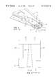
- FIG. 1is a planar view of an exemplary magnetic disk drive
- FIG. 2is an end view of a slider with a magnetic head of the disk drive as seen in plane 2 — 2 ;
- FIG. 3is an elevation view of the magnetic disk drive wherein multiple disks and magnetic heads are employed
- FIG. 4is an isometric illustration of an exemplary suspension system for supporting the slider and magnetic head
- FIG. 5is an ABS view of the magnetic head taken along plane 5 — 5 of FIG. 2;
- FIG. 6is a partial cross-sectional view of the prior art magnetic head as seen in plane 6 — 6 of FIG. 2;
- FIG. 7is a enlarged partial ABS view of the slider taken along plane 7 — 7 of FIG. 6 to show the read and write elements of the prior art magnetic head;
- FIGS. 8 and 9are views taken along plane 8 — 8 and 9 — 9 of FIG. 6 illustrating the prior art
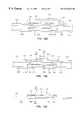
- FIG. 10is a partial cross-sectional view of the preferred embodiment magnetic head as seen in plane 10 — 10 of FIG. 2;
- FIG. 11is a view taken along plane 11 — 11 -of FIG., 10 illustrating the present invention
- FIGS. 12A and 12Bare views taken along plane 12 A— 12 A and 12 B— 12 B of FIG. 11 illustrating the present invention.
- FIGS. 13A-13Dillustrate some of the processing steps to planarized the surface at the second shield layer.
- the drive 30includes a spindle 32 that supports and rotates a magnetic disk 34 .
- the spindle 32is rotated by a motor 36 that is controlled by a motor controller 38 .
- a read/write magnetic head 40is mounted on a slider 42 that is supported by a suspension 44 and actuator arm 46 .
- a plurality of disks, sliders and suspensionsmay be employed in a large capacity direct access storage device (DASD) as shown in FIG. 3 .
- DASDdirect access storage device
- the suspension 44 and actuator arm 46position the slider 42 so that the magnetic head 40 is in a transducing relationship with a surface of the magnetic disk 34 .
- the sliderWhen the disk 34 is rotated by the motor 36 the slider is supported on a thin (typically, 0.05 ⁇ m) cushion of air (air bearing) between the surface of the disk 34 and the air bearing surface (ABS) 48 .
- the magnetic head 40may then be employed for writing information to multiple circular tracks on the surface of the disk 34 , as well as for reading information therefrom.
- Processing circuitry 50exchanges signals, representing such information, with the head 40 , provides motor drive signals for rotating the magnetic disk 34 , and provides control signals for moving the slider to various tracks.
- the slider 42In FIG. 4 the slider 42 is shown mounted to the suspension 44 .
- the components described hereinabovemay be mounted on a frame 54 of a housing 55 , as shown in FIG. 3 .
- FIG. 5is an ABS view of the slider 42 and the magnetic head 40 .
- the sliderhas a center rail 56 that supports the magnetic head 40 , and side rails 58 and 60 .
- the rails 56 , 58 and 60extend from a cross rail 62 .
- the cross rail 62is at a leading edge 64 of the slider and the magnetic head 40 is at a trailing edge 66 of the slider.
- FIG. 6is a side cross-sectional elevation view of the merged magnetic head 40 which has a prior art write head portion 70 and a read head portion 71 , the read head portion employing an MR sensor 74 .
- FIG. 7is ABS view of FIG. 6 .
- the sensor 74is located between first and second gap layers 76 and 78 and the gap layers are located between first and second shield layers 80 and 82 .
- the resistance of the sensor 74changes.
- a sense current I S conducted through the sensor 74causes these resistance changes to be manifested as potential changes. These potential changes are then processed as readback signals by the processing circuitry 50 shown in FIG. 3 .
- the shielding layers 80 and 82typically comprise a soft ferromagnetic material such as sendust or NiFe, and are formed by conventional methods such as chemical vapor deposition (CVD) or sputtering or plating.
- Shield layer 80is formed on a substrate 72 , being separated by a undercoat 73 .
- the gap layers 76 and 78comprise any material suitable for electrically isolating the conductive layers of the read head, e.g., Al 2 O 3 , SiO 2 , etc.
- the prior art write head portion 70 of the merged MR headincludes an inductive coil layer 84 located in insulation layers 86 and 87 .
- the coil layer 84 and insulation layers 86are located between first and second pole piece layers 92 and 94 .
- the first and second pole piece layers 92 and 94are magnetically coupled at a back gap 96 and have first and second pole tips 98 and 100 which are separated by a write gap layer 102 at the ABS.
- An overpass conductor 90provides electrical coupling between a write pad and the inner tap 91 of the inductive coil 84 .
- the conductor 90has access to the inner coil tap 91 through a via 89 in the insulation 87 .
- the coil 84is provided with two electrical leads, at an inner tap 91 and at an outer tap (not shown).
- a write current I in sent through the electrical leads and the coil 84the current I produces a flux.
- the fluxprovides a substantial magnetomotive potential difference between first pole tip 98 and second pole tip 100 which provides an efficient write process.
- first and second terminal pads 104 and 106connect to leads 112 and 114 on the suspension 44 and third and fourth terminal pads 116 and 118 connect to leads 124 and 126 on the suspension.
- a wear layer 128may be employed for protecting the sensitive elements of the magnetic head, as shown in FIGS. 2 and 4. It should be noted that the illustrated magnetic head 40 employs a single layer 82 / 92 to serve a double function as a second shield layer S 2 for the read head and as a first pole piece PI for the write head. A piggyback MR head employs two separate layers for these functions.
- FIG. 7shows an ABS view of the read/write head 40 .
- FIGS. 8 and 9show cross-sectional views of FIG. 6 .
- the layers used in forming the head 40form a bulge with steps near the outer edges. Attempts have been tried to planarize the head 40 above the second shield layer 82 (S 2 ) level so that the layer for the coil 84 is relatively flat. Prior art heads accomplish this planarization by starting with an excessively large first shield layer 80 .
- hard bake resistis used to provide build up for the pseudo planarization for the coil 84 .
- thisalso creates steps for the leads 20 at the edge of the head 40 where the leads travel from the head 40 to the pads 21 . This excessive topography for the leads 20 can result in shorting paths around the edges 22 of the hard bake regions and shields. Additionally, the leads and pads are separated from the substrate by only the undercoat 73 .
- the merged read/write head 140 of the present inventionimproves the device topography by creating a planar structure such that the pads 121 and leads 120 are on the same plane.
- a planarizing layer of materialis used, to not only planarize the area under the coil, but also planarize the entire device surface, all the way out to the pads at the outer edge.
- the leads connecting the MR sensor or coil and the padsare parallel to the substrate surface and on a plane defined by the top of the second shield layer S 2 (i.e., all the pads and leads are coplanar). This virtually eliminates any shorts or opens of the leads due to steps.
- the separation between the pads and substrateare substantially increased, thereby reducing the capacitance coupling between the conducting undercoat layer and the pads.
- the first shield layer and the substratemay now be in direct contact (i.e., no undercoat alumina required). Reducing the size of the first shield layer thereby reduces the hard baked resist area, since the resist does not need to extend past the outer perimeter of the first shield layer, thus increasing the region where the pads can be safely positioned (i.e., the pads should not overlap any underlying hard baked resist).
- FIG. 10is a side cross-sectional elevation view of the head 140 of the present invention which includes a write head portion 170 and a read head portion 171 , the read head portion 171 employing an MR sensor 174 .
- the resistance of the MR sensor 174changes.
- a sense current Is conducted through the MR sensor 174causes these resistance changes to be manifested as potential changes.
- These potential changesare then processed as readback signals by the processing circuitry 50 shown in FIG. 3 .
- FIG. 11shows a planar view with portions of the upper layers removed for clarity.
- FIGS. 12A and 12Bshow cross-sectional views of FIG. 10 .
- the sensor 174is located between first and second gap layers 176 and 178 and the gap layers are located between first and second shield layers 180 and 182 .
- the first shield layer 180is essentially the same length as the second shield layer 182 , which is shorter than coil 184 .
- the shields 180 and 182may be shorter or longer depending on the minimum shielding requirements of the MR sensor 174 used.
- a planarizing layer 188is used to planarize the entire device at the second shield layer 182 (the S 2 layer). Planarizing layer 188 may be made of Al 2 O 3 .
- the shielding layers 180 , 182typically comprise a soft ferromagnetic material such as sendust or NiFe, and are formed by conventional methods such as chemical vapor deposition (CVD) or sputtering or plating.
- Shield layer 180is formed on a substrate 172 , and may be separated by an undercoat 173 .
- the gap layers 176 , 178comprise any material suitable for electrically isolating the conductive layers of the read head, e.g., SiO 2 , etc.
- the write head portion 170 of the merged MR head 140includes an inductive coil 184 .
- the coil 184is positioned inside of insulation layers 186 and 187 .
- a portion of the coil 184 along with insulation layer 186are located between first and second pole piece layers 192 and 194 .
- the remainder of the coilis inside of insulation layers 186 and 187 being formed on the planarizing layer 188 .
- the first and second pole piece layers 192 and 194are magnetically coupled at a back gap 196 and have first and second pole tips 198 and 200 which are separated by a write gap layer 202 at the ABS.
- An overpass conductor 190provides electrical coupling between a pad 121 and the inner tap 220 of the inductive coil 184 .
- the conductor 190has access to the inner coil tap 220 through a via 189 in the insulation 186 .
- first and second terminal pads 104 and 106connect to leads 112 and 114 on the suspension 44 .
- Third and fourth terminal pads 116 and 118connect to leads 124 and 126 on the suspension 44 .
- Leads 120 and pads 121are formed on the planar layer.
- the leads 120are connected by vias 123 and copper studs 125 to the MR sensor leads 145 and 146 .
- a wear layer(not shown) may be employed for protecting the sensitive elements of the magnetic head, as shown in FIGS. 2 and 4.
- the merged MR head 140employs a single layer 182 / 192 to serve a double function as a second shield layer S 2 for the read head and as a first pole piece P 1 for the write head.
- a piggyback MR heademploys two separate layers for these functions.
- the various layers of the method of makingare formed by sputter deposition or plating.
- the metallic layersare formed by plating and the non-conductive layers are formed by sputter deposition or forming hard baked photoresist.
- Sputter depositionis implemented in a vacuum chamber wherein a target of desired material is sputtered to a substrate via a plasma in the chamber because of an applied potential between the target and the substrate.
- Platingis a wet process wherein the wafer is placed in an electrolyte and a potential is applied between the surface to be plated and a plating material. Metallic ions from the plating material are then deposited on the desired surface.
- Photoresist maskswhich are spun onto the wafer, imaged with light and then portions to be removed are removed by a developer.
- Positive photoresistmay be employed wherein the area of light imaging is removed by a developer to provide an opening for plating or a negative photoresist (cross-linked photoresist) may be employed where an area not imaged by light is removed by the developer to provide an opening for plating.
- a dissolventAfter the desired layer is deposited the photoresist mask is then stripped by a dissolvent. Layer portions are removed by ion milling which, in essence, is particle bombardment of the layer with ions. It should be understood that these process steps are exemplary and there may be other steps well known in the art for forming the layers.
- the shields and pole piecesare preferably Permalloy which is Ni 80 Fe 20 . If desired, a higher magnetic moment material may be employed for the second pole piece such as Ni 45 Fe 55 .
- the insulation layers of the insulationare preferably photoresist, except the first insulation layer and the planarizing layer which are preferably alumina (Al 2 O 3 ). Because of the present inventions unique design of minimizing the shield layers, the amount of photoresist is also minimized. After each photoresist layer is patterned, it is hard baked, such as at a temperature of 200° C., which provides each layer with sloping surfaces at its edges.
- the insulation layersmay be another insulation material, such as alumina (Al 2 O 3 ) or silicon dioxide (SiO 2 ).
- the write gap layeris preferably alumina and formed by sputtering.
- the pole piece layersare frame plated which comprises patterning with photoresist, plating into the opening in the photoresist and then removing the photoresist. If the pole piece layer is formed on a nonmagnetic layer, such as alumina or baked photoresist, a seedlayer, such as copper or Permalloy, is sputtered on the layer to provide a return path for electroplating.
- a copper seedlayeris employed before the frame plating of a coil layer, after which the seedlayer is removed by ion milling without any patterning.
- a metallic layeris normally constructed by frame plating.
- Frame platingcomprises sputtering a seedlayer on the underlying layer if the underlying layer is electrically non-conductive, spinning a photoresist layer on the underlying layer, light imaging the photoresist layer in areas that are to be opened, developing the exposed regions of the photoresist to provide openings, or an opening, exposing the seedlayer where a metallic layer is to be plated, plating the metallic layer by electroplating, stripping the photoresist layer with a solvent and removing any seedlayer by ion milling.
- FIGS. 13A-13Dillustrated a planarization process for the formation of a planarized surface at the S 2 (second shield) layer.
- the first shield layer 180is formed on a substrate 172 .
- a layer of undercoat 173may be positioned between the first shield layer 180 and the substrate 172 .
- the first shield layer 180being sized to shield the MR sensor 174 .
- a first gap layer 176is formed on the first shield layer 180 by conventional means.
- the MR sensor 174is then formed by subtractive etching or another suitable process, and sensor leads 144 and 145 are formed thereon by methods such as electroplating or sputtering.
- a second gap layer 178is then formed over the sensor 174 and leads 144 and 145 .
- the second shield layer 182is formed over the second gap layer 178 completing the read portion 171 of the head 140 .
- Vias 123are opened to expose the sensor leads.
- Copper studs 125are plated into the vias to a thickness greater than the height of the S 2 (second shield 182 ) surface.
- a planarizing layer 188is applied to planarize the head at the S 2 level.
- Planarizing layer 188is preferably made from a electrically isolating material, such as Al 2 O 3 and may be fabricated on a single layer (as shown in the figures) or may be separate layers. Once formed, the planarization layer 188 may be planarized by chemical mechanical polishing (CMP) or other suitable means of planarization to form a planar surface.
- CMPchemical mechanical polishing
Landscapes
- Engineering & Computer Science (AREA)
- Chemical & Material Sciences (AREA)
- Nanotechnology (AREA)
- Crystallography & Structural Chemistry (AREA)
- Manufacturing & Machinery (AREA)
- Physics & Mathematics (AREA)
- Mathematical Physics (AREA)
- Theoretical Computer Science (AREA)
- Magnetic Heads (AREA)
Abstract
Description
Claims (109)
Priority Applications (1)
| Application Number | Priority Date | Filing Date | Title |
|---|---|---|---|
| US09/320,480US6324036B1 (en) | 1999-05-26 | 1999-05-26 | Combination inductive write head and magnetoresistive (MR) read head with improved topography |
Applications Claiming Priority (1)
| Application Number | Priority Date | Filing Date | Title |
|---|---|---|---|
| US09/320,480US6324036B1 (en) | 1999-05-26 | 1999-05-26 | Combination inductive write head and magnetoresistive (MR) read head with improved topography |
Publications (1)
| Publication Number | Publication Date |
|---|---|
| US6324036B1true US6324036B1 (en) | 2001-11-27 |
Family
ID=23246622
Family Applications (1)
| Application Number | Title | Priority Date | Filing Date |
|---|---|---|---|
| US09/320,480Expired - LifetimeUS6324036B1 (en) | 1999-05-26 | 1999-05-26 | Combination inductive write head and magnetoresistive (MR) read head with improved topography |
Country Status (1)
| Country | Link |
|---|---|
| US (1) | US6324036B1 (en) |
Cited By (15)
| Publication number | Priority date | Publication date | Assignee | Title |
|---|---|---|---|---|
| US20020057537A1 (en)* | 2000-08-15 | 2002-05-16 | Seagate Technology Llc | Ion mill shutter system |
| US6671134B1 (en)* | 1999-07-16 | 2003-12-30 | Tdk Corporation | Thin film magnetic head and method of manufacturing the same |
| US6674610B1 (en)* | 2000-06-16 | 2004-01-06 | Western Digital (Fremont), Inc. | Thin film write head with universal coil design |
| US20040057146A1 (en)* | 2002-09-25 | 2004-03-25 | International Business Machines Corporation | Method and apparatus for balanced shield shunts, leads and pads for electrical noise reduction in read heads |
| US20040062152A1 (en)* | 2002-09-27 | 2004-04-01 | Stancil Daniel D. | Device for writing data to a recording medium and method of fabricating same |
| US20050146811A1 (en)* | 2002-08-07 | 2005-07-07 | Headway Technologies, Inc. | Method for suppressing tribocharge in the assembly of magnetic heads |
| US20060087770A1 (en)* | 2004-10-27 | 2006-04-27 | Hitachi Global Storage Technologies Netherlands B.V. | Magnetic recording head for perpendicular recording, fabrication process, and magnetic disk storage apparatus mounting the magnetic recording head |
| US20060099890A1 (en)* | 2002-01-14 | 2006-05-11 | Florence Eschbach | Simultaneous planarization of pole piece and coil materials for write head applications |
| US7054113B1 (en)* | 2001-10-25 | 2006-05-30 | Western Digital (Fremont), Inc. | Reader/writer for magnetic memory |
| US20070008657A1 (en)* | 2005-06-07 | 2007-01-11 | Fujitsu Limited | Magnetic head including read head element and inductive write head element |
| CN100342427C (en)* | 2004-03-31 | 2007-10-10 | Tdk株式会社 | Composite type thin-film magnetic head |
| US20090168259A1 (en)* | 2007-12-31 | 2009-07-02 | Arley Cleveland Marley | Wafer level balanced capacitance design for magnetic heads |
| US20110175606A1 (en)* | 2010-01-21 | 2011-07-21 | Daido Tokushuko Kabushiki Kaisha | Thin-film magnetic sensor and method for manufacturing the same |
| US8670214B1 (en)* | 2011-12-20 | 2014-03-11 | Western Digital (Fremont), Llc | Method and system for providing enhanced thermal expansion for hard disk drives |
| US8749920B1 (en) | 2011-12-16 | 2014-06-10 | Western Digital (Fremont), Llc | Magnetic recording head with dynamic fly height heating and having thermally controlled pole tip protrusion to control and protect reader element |
Citations (14)
| Publication number | Priority date | Publication date | Assignee | Title |
|---|---|---|---|---|
| US3908194A (en) | 1974-08-19 | 1975-09-23 | Ibm | Integrated magnetoresistive read, inductive write, batch fabricated magnetic head |
| SU902060A1 (en) | 1978-03-16 | 1982-01-30 | Минский радиотехнический институт | Integral magnetic head |
| US4423451A (en) | 1981-08-10 | 1983-12-27 | Sperry Corporation | Thin film magnetic head having disparate poles for pulse asymmetry compensation |
| US4523243A (en) | 1982-05-24 | 1985-06-11 | Storage Technology Corporation | Magnetoresistive transducer using an independent recessed electromagnetic bias |
| JPS61120318A (en) | 1984-11-15 | 1986-06-07 | Matsushita Electric Ind Co Ltd | Unified thin film magnetic head |
| JPH05197920A (en) | 1992-01-20 | 1993-08-06 | Mitsubishi Electric Corp | Thin film magnetic head and its production |
| US5272582A (en) | 1990-09-28 | 1993-12-21 | Sony Corporation | Magneto-resistance effect magnetic head with static electricity protection |
| US5486968A (en) | 1993-11-10 | 1996-01-23 | International Business Machines Corporation | Method and apparatus for simultaneous write head planarization and lead routing |
| US5557491A (en) | 1994-08-18 | 1996-09-17 | International Business Machines Corporation | Two terminal single stripe orthogonal MR head having biasing conductor integral with the lead layers |
| US5557492A (en) | 1993-08-06 | 1996-09-17 | International Business Machines Corporation | Thin film magnetoresistive head with reduced lead-shield shorting |
| US5617275A (en) | 1994-05-02 | 1997-04-01 | Sanyo Electric Co., Ltd. | Thin film head having a core comprising Fe-N-O in a specific atomic composition ratio |
| US5691867A (en) | 1995-07-05 | 1997-11-25 | Sony Corporation | Complex type thin film magnetic head and production method thereof |
| US5694276A (en)* | 1996-07-01 | 1997-12-02 | Read-Rite Corporation | Shielded magnetic head having an inductive coil with low mutual inductance |
| US5742459A (en) | 1996-06-20 | 1998-04-21 | Read-Rite Corporation | Magnetic head having encapsulated magnetoresistive transducer and multilayered lead structure |
- 1999
- 1999-05-26USUS09/320,480patent/US6324036B1/ennot_activeExpired - Lifetime
Patent Citations (15)
| Publication number | Priority date | Publication date | Assignee | Title |
|---|---|---|---|---|
| US3908194A (en) | 1974-08-19 | 1975-09-23 | Ibm | Integrated magnetoresistive read, inductive write, batch fabricated magnetic head |
| SU902060A1 (en) | 1978-03-16 | 1982-01-30 | Минский радиотехнический институт | Integral magnetic head |
| US4423451A (en) | 1981-08-10 | 1983-12-27 | Sperry Corporation | Thin film magnetic head having disparate poles for pulse asymmetry compensation |
| US4523243A (en) | 1982-05-24 | 1985-06-11 | Storage Technology Corporation | Magnetoresistive transducer using an independent recessed electromagnetic bias |
| JPS61120318A (en) | 1984-11-15 | 1986-06-07 | Matsushita Electric Ind Co Ltd | Unified thin film magnetic head |
| US5272582A (en) | 1990-09-28 | 1993-12-21 | Sony Corporation | Magneto-resistance effect magnetic head with static electricity protection |
| JPH05197920A (en) | 1992-01-20 | 1993-08-06 | Mitsubishi Electric Corp | Thin film magnetic head and its production |
| US5557492A (en) | 1993-08-06 | 1996-09-17 | International Business Machines Corporation | Thin film magnetoresistive head with reduced lead-shield shorting |
| US5486968A (en) | 1993-11-10 | 1996-01-23 | International Business Machines Corporation | Method and apparatus for simultaneous write head planarization and lead routing |
| US5761013A (en)* | 1993-11-10 | 1998-06-02 | International Business Machines Corporation | Apparatus for simultaneous write head planarization and lead routing |
| US5617275A (en) | 1994-05-02 | 1997-04-01 | Sanyo Electric Co., Ltd. | Thin film head having a core comprising Fe-N-O in a specific atomic composition ratio |
| US5557491A (en) | 1994-08-18 | 1996-09-17 | International Business Machines Corporation | Two terminal single stripe orthogonal MR head having biasing conductor integral with the lead layers |
| US5691867A (en) | 1995-07-05 | 1997-11-25 | Sony Corporation | Complex type thin film magnetic head and production method thereof |
| US5742459A (en) | 1996-06-20 | 1998-04-21 | Read-Rite Corporation | Magnetic head having encapsulated magnetoresistive transducer and multilayered lead structure |
| US5694276A (en)* | 1996-07-01 | 1997-12-02 | Read-Rite Corporation | Shielded magnetic head having an inductive coil with low mutual inductance |
Non-Patent Citations (1)
| Title |
|---|
| "Buried Stud Planar Attach Head", IBM Technical Disclosure Bulletin, pp. 73-76, vol. 39, No. 10, Oct. 1996. |
Cited By (25)
| Publication number | Priority date | Publication date | Assignee | Title |
|---|---|---|---|---|
| US6671134B1 (en)* | 1999-07-16 | 2003-12-30 | Tdk Corporation | Thin film magnetic head and method of manufacturing the same |
| US6674610B1 (en)* | 2000-06-16 | 2004-01-06 | Western Digital (Fremont), Inc. | Thin film write head with universal coil design |
| US20020057537A1 (en)* | 2000-08-15 | 2002-05-16 | Seagate Technology Llc | Ion mill shutter system |
| US7144484B2 (en) | 2000-08-15 | 2006-12-05 | Seagate Technology Llc | Ion mill shutter system |
| US7054113B1 (en)* | 2001-10-25 | 2006-05-30 | Western Digital (Fremont), Inc. | Reader/writer for magnetic memory |
| US20060099890A1 (en)* | 2002-01-14 | 2006-05-11 | Florence Eschbach | Simultaneous planarization of pole piece and coil materials for write head applications |
| US7201637B2 (en)* | 2002-01-14 | 2007-04-10 | Hitachi Global Storage Technologies Netherlands B.V. | Simultaneous planarization of pole piece and coil materials for write head applications |
| US20050146811A1 (en)* | 2002-08-07 | 2005-07-07 | Headway Technologies, Inc. | Method for suppressing tribocharge in the assembly of magnetic heads |
| US7190556B2 (en)* | 2002-08-07 | 2007-03-13 | Headway Technologies, Inc, | Method for suppressing tribocharge in the assembly of magnetic heads |
| US7508613B2 (en) | 2002-09-25 | 2009-03-24 | Hitachi Global Storage Technologies Netherlands B.V. | Method and apparatus for balanced shield shunts, leads and pads for electrical noise reduction in read heads |
| US20070211373A1 (en)* | 2002-09-25 | 2007-09-13 | Hitachi Global Storage Technologies Netherlands B.V. | Method and Apparatus For Balanced Shield Shunts, Leads and Pads For Electrical Noise Reduction in Read Heads |
| US20040057146A1 (en)* | 2002-09-25 | 2004-03-25 | International Business Machines Corporation | Method and apparatus for balanced shield shunts, leads and pads for electrical noise reduction in read heads |
| US7206154B2 (en) | 2002-09-25 | 2007-04-17 | Hitachi Global Storage Technologies Netherlands, B.V. | Method and apparatus for balanced shield shunts, leads and pads for electrical noise reduction in read heads |
| US6999384B2 (en) | 2002-09-27 | 2006-02-14 | Carnegie Mellon University | Device with waveguide defined by dielectric in aperture of cross-track portion of electrical conductor for writing data to a recording medium |
| US20040062152A1 (en)* | 2002-09-27 | 2004-04-01 | Stancil Daniel D. | Device for writing data to a recording medium and method of fabricating same |
| CN100342427C (en)* | 2004-03-31 | 2007-10-10 | Tdk株式会社 | Composite type thin-film magnetic head |
| US20060087770A1 (en)* | 2004-10-27 | 2006-04-27 | Hitachi Global Storage Technologies Netherlands B.V. | Magnetic recording head for perpendicular recording, fabrication process, and magnetic disk storage apparatus mounting the magnetic recording head |
| US7755864B2 (en)* | 2004-10-27 | 2010-07-13 | Hitachi Global Storage Technologies Netherlands B.V. | Magnetic recording head for perpendicular recording, fabrication process, and magnetic disk storage apparatus mounting the magnetic recording head |
| US20070008657A1 (en)* | 2005-06-07 | 2007-01-11 | Fujitsu Limited | Magnetic head including read head element and inductive write head element |
| US20090168259A1 (en)* | 2007-12-31 | 2009-07-02 | Arley Cleveland Marley | Wafer level balanced capacitance design for magnetic heads |
| US8089295B2 (en) | 2007-12-31 | 2012-01-03 | Hitachi Global Storage Technologies Netherlands B.V. | Wafer level balanced capacitance design for magnetic heads |
| US20110175606A1 (en)* | 2010-01-21 | 2011-07-21 | Daido Tokushuko Kabushiki Kaisha | Thin-film magnetic sensor and method for manufacturing the same |
| US9304176B2 (en)* | 2010-01-21 | 2016-04-05 | Daido Tokushuko Kabushiki Kaisha | Thin-film magnetic sensor including a GMR film and method for manufacturing the same |
| US8749920B1 (en) | 2011-12-16 | 2014-06-10 | Western Digital (Fremont), Llc | Magnetic recording head with dynamic fly height heating and having thermally controlled pole tip protrusion to control and protect reader element |
| US8670214B1 (en)* | 2011-12-20 | 2014-03-11 | Western Digital (Fremont), Llc | Method and system for providing enhanced thermal expansion for hard disk drives |
Similar Documents
| Publication | Publication Date | Title |
|---|---|---|
| US6104576A (en) | Inductive head with reduced height insulation stack due to partial coverage zero throat height defining insulation layer | |
| US6693769B2 (en) | High data rate write head | |
| US7386933B1 (en) | Method of fabricating thin film write heads with a shortened yoke and improved dimension control | |
| US7612963B2 (en) | Perpendicular magnetic recording head with photoresist dam between write coil and air bearing surface | |
| KR100458845B1 (en) | Read head with read track width defining layer that planarizes the write gap layer of a write head | |
| US7054117B2 (en) | Method of making a read head having a tunnel junction sensor with a free layer biased by exchange coupling with insulating antiferromagnetic (AFM) layers | |
| US6324036B1 (en) | Combination inductive write head and magnetoresistive (MR) read head with improved topography | |
| US6785953B2 (en) | Process of fabricating a write head with protection of a second pole tip thickness | |
| US6722018B2 (en) | Method of forming a second pole piece of a write head | |
| US20030137781A1 (en) | Flux guide read head with in stack biased current perpendicular to the planes (CPP) sensor | |
| US6510030B1 (en) | Transducing head and method for forming a recessed shield for a transducing head | |
| US7532441B2 (en) | MR read head with first and second gap layers | |
| WO1998040880A1 (en) | Magnetic head having dielectric isolator elements | |
| US6301084B1 (en) | Protection of second pole tip during fabrication of write head | |
| US5936811A (en) | Magnetic head with vialess lead layers from MR sensor to pads | |
| US7765677B2 (en) | Method for manufacturing a magnetic write head using a protective layer to prevent write pole consumption | |
| US7187520B2 (en) | Magnetic head having thermally assisted recording device, and method of fabrication thereof | |
| US6525913B1 (en) | Read head with sunken prefill insulation for preventing lead to shield shorts and maintaining planarization | |
| US8270124B2 (en) | Magnetic head having reduced cost electrostatic discharge shunt | |
| US5694276A (en) | Shielded magnetic head having an inductive coil with low mutual inductance | |
| JP2005012215A (en) | Magnetoresistive sensor with a bias magnet with steep end walls | |
| US7768748B2 (en) | Magnetoresistive sensor with overlaid combined leads and shields | |
| US20060034012A1 (en) | Self-aligned coil process in magnetic recording heads |
Legal Events
| Date | Code | Title | Description |
|---|---|---|---|
| AS | Assignment | Owner name:INTERNATIONAL BUSINESS MACHINES CORPORATION, NEW Y Free format text:ASSIGNMENT OF ASSIGNORS INTEREST;ASSIGNORS:DILL, FREDERICK HAYES JR.;FONTANA, ROBERT E., JR.;LEE, EDWARD HIN PONG;REEL/FRAME:010001/0401;SIGNING DATES FROM 19990503 TO 19990520 | |
| STCF | Information on status: patent grant | Free format text:PATENTED CASE | |
| AS | Assignment | Owner name:MARIANA HDD B.V., NETHERLANDS Free format text:ASSIGNMENT OF ASSIGNORS INTEREST;ASSIGNOR:INTERNATIONAL BUSINESS MACHINES CORPORATION;REEL/FRAME:013663/0348 Effective date:20021231 | |
| AS | Assignment | Owner name:HITACHI GLOBAL STORAGE TECHNOLOGIES NETHERLANDS B. Free format text:CHANGE OF NAME;ASSIGNOR:MARIANA HDD B.V.;REEL/FRAME:013746/0146 Effective date:20021231 | |
| FEPP | Fee payment procedure | Free format text:PAYOR NUMBER ASSIGNED (ORIGINAL EVENT CODE: ASPN); ENTITY STATUS OF PATENT OWNER: LARGE ENTITY | |
| FPAY | Fee payment | Year of fee payment:4 | |
| FPAY | Fee payment | Year of fee payment:8 | |
| AS | Assignment | Owner name:HGST, NETHERLANDS B.V., NETHERLANDS Free format text:CHANGE OF NAME;ASSIGNOR:HGST, NETHERLANDS B.V.;REEL/FRAME:029341/0777 Effective date:20120723 Owner name:HGST NETHERLANDS B.V., NETHERLANDS Free format text:CHANGE OF NAME;ASSIGNOR:HITACHI GLOBAL STORAGE TECHNOLOGIES NETHERLANDS B.V.;REEL/FRAME:029341/0777 Effective date:20120723 | |
| FPAY | Fee payment | Year of fee payment:12 | |
| AS | Assignment | Owner name:WESTERN DIGITAL TECHNOLOGIES, INC., CALIFORNIA Free format text:ASSIGNMENT OF ASSIGNORS INTEREST;ASSIGNOR:HGST NETHERLANDS B.V.;REEL/FRAME:040818/0551 Effective date:20160831 |