US6323522B1 - Silicon on insulator thick oxide structure and process of manufacture - Google Patents
Silicon on insulator thick oxide structure and process of manufactureDownload PDFInfo
- Publication number
- US6323522B1 US6323522B1US09/227,695US22769599AUS6323522B1US 6323522 B1US6323522 B1US 6323522B1US 22769599 AUS22769599 AUS 22769599AUS 6323522 B1US6323522 B1US 6323522B1
- Authority
- US
- United States
- Prior art keywords
- transistor
- thick oxide
- drain
- gate
- width
- Prior art date
- Legal status (The legal status is an assumption and is not a legal conclusion. Google has not performed a legal analysis and makes no representation as to the accuracy of the status listed.)
- Expired - Lifetime
Links
Images


Classifications
- H—ELECTRICITY
- H10—SEMICONDUCTOR DEVICES; ELECTRIC SOLID-STATE DEVICES NOT OTHERWISE PROVIDED FOR
- H10D—INORGANIC ELECTRIC SEMICONDUCTOR DEVICES
- H10D30/00—Field-effect transistors [FET]
- H10D30/60—Insulated-gate field-effect transistors [IGFET]
- H—ELECTRICITY
- H10—SEMICONDUCTOR DEVICES; ELECTRIC SOLID-STATE DEVICES NOT OTHERWISE PROVIDED FOR
- H10D—INORGANIC ELECTRIC SEMICONDUCTOR DEVICES
- H10D86/00—Integrated devices formed in or on insulating or conducting substrates, e.g. formed in silicon-on-insulator [SOI] substrates or on stainless steel or glass substrates
- H10D86/201—Integrated devices formed in or on insulating or conducting substrates, e.g. formed in silicon-on-insulator [SOI] substrates or on stainless steel or glass substrates the substrates comprising an insulating layer on a semiconductor body, e.g. SOI
- H—ELECTRICITY
- H10—SEMICONDUCTOR DEVICES; ELECTRIC SOLID-STATE DEVICES NOT OTHERWISE PROVIDED FOR
- H10D—INORGANIC ELECTRIC SEMICONDUCTOR DEVICES
- H10D30/00—Field-effect transistors [FET]
- H10D30/60—Insulated-gate field-effect transistors [IGFET]
- H10D30/67—Thin-film transistors [TFT]
- H10D30/6704—Thin-film transistors [TFT] having supplementary regions or layers in the thin films or in the insulated bulk substrates for controlling properties of the device
- H10D30/6708—Thin-film transistors [TFT] having supplementary regions or layers in the thin films or in the insulated bulk substrates for controlling properties of the device for preventing the kink effect or the snapback effect, e.g. discharging the minority carriers of the channel region for preventing bipolar effect
- H10D30/6711—Thin-film transistors [TFT] having supplementary regions or layers in the thin films or in the insulated bulk substrates for controlling properties of the device for preventing the kink effect or the snapback effect, e.g. discharging the minority carriers of the channel region for preventing bipolar effect by using electrodes contacting the supplementary regions or layers
- H—ELECTRICITY
- H10—SEMICONDUCTOR DEVICES; ELECTRIC SOLID-STATE DEVICES NOT OTHERWISE PROVIDED FOR
- H10D—INORGANIC ELECTRIC SEMICONDUCTOR DEVICES
- H10D30/00—Field-effect transistors [FET]
- H10D30/60—Insulated-gate field-effect transistors [IGFET]
- H10D30/67—Thin-film transistors [TFT]
- H10D30/6729—Thin-film transistors [TFT] characterised by the electrodes
- H10D30/6737—Thin-film transistors [TFT] characterised by the electrodes characterised by the electrode materials
- H10D30/6739—Conductor-insulator-semiconductor electrodes
- H—ELECTRICITY
- H10—SEMICONDUCTOR DEVICES; ELECTRIC SOLID-STATE DEVICES NOT OTHERWISE PROVIDED FOR
- H10D—INORGANIC ELECTRIC SEMICONDUCTOR DEVICES
- H10D30/00—Field-effect transistors [FET]
- H10D30/60—Insulated-gate field-effect transistors [IGFET]
- H10D30/67—Thin-film transistors [TFT]
- H10D30/6757—Thin-film transistors [TFT] characterised by the structure of the channel, e.g. transverse or longitudinal shape or doping profile
- H—ELECTRICITY
- H10—SEMICONDUCTOR DEVICES; ELECTRIC SOLID-STATE DEVICES NOT OTHERWISE PROVIDED FOR
- H10D—INORGANIC ELECTRIC SEMICONDUCTOR DEVICES
- H10D89/00—Aspects of integrated devices not covered by groups H10D84/00 - H10D88/00
- H10D89/60—Integrated devices comprising arrangements for electrical or thermal protection, e.g. protection circuits against electrostatic discharge [ESD]
- H10D89/601—Integrated devices comprising arrangements for electrical or thermal protection, e.g. protection circuits against electrostatic discharge [ESD] for devices having insulated gate electrodes, e.g. for IGFETs or IGBTs
- H10D89/811—Integrated devices comprising arrangements for electrical or thermal protection, e.g. protection circuits against electrostatic discharge [ESD] for devices having insulated gate electrodes, e.g. for IGFETs or IGBTs using FETs as protective elements
- H—ELECTRICITY
- H01—ELECTRIC ELEMENTS
- H01L—SEMICONDUCTOR DEVICES NOT COVERED BY CLASS H10
- H01L2924/00—Indexing scheme for arrangements or methods for connecting or disconnecting semiconductor or solid-state bodies as covered by H01L24/00
- H01L2924/0001—Technical content checked by a classifier
- H01L2924/0002—Not covered by any one of groups H01L24/00, H01L24/00 and H01L2224/00
Definitions
- the present inventionrelates, in general, to a silicon-on-insulator (SOI) type semiconductor device and, more specifically, to a body-and-gate-coupled thick oxide structure providing electrostatic discharge (ESD) protection in a network.
- SOIsilicon-on-insulator
- ESDelectrostatic discharge
- Protection networksare typically used in integrated circuits to protect internal components from ESD.
- componentsmay be fabricated to dissipate excess charge during an ESD event.
- Common types of components used for ESD protectioninclude metal oxide semiconductor field effect transistors (MOSFETs) and thick field oxide (TFO) punch-through devices.
- MOSFETsmetal oxide semiconductor field effect transistors
- TFOthick field oxide
- the breakdown voltage of the componentis determined by the breakdown voltage of a p-n junction within the component. The area of the p-n junction is usually large enough to be able to dissipate the excess charge during an ESD event.
- Assaderaghi et al.disclose a SOI circuit which includes a body-coupled-gated (BCG) diode formed from a SOI MOSFET for providing ESD protection. Both NMOSFETs and PMOSFETs may be used to create a forward-biased operation of the diode.
- BCGbody-coupled-gated
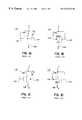
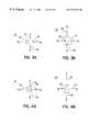
- NMOSFET 100comprises a source 108 , drain 106 , body 104 , and gate 102 .
- the drain, body, and gateare connected at node A.
- node Ais greater in voltage than node B, NMOSFET 100 turns on, thus providing ESD protection.
- NMOSFET 100may be represented by the diode symbol, as shown in FIG. 1 b.
- a PMOSFET 110comprises a source 108 , drain 106 , body 104 , and gate 102 .
- the drain, body, and gateare connected at node A.
- node Bis greater in voltage than node A
- PMOSFET 110turns on, thus providing ESD protection.
- PMOSFET 110may be represented by the diode symbol, as shown in FIG. 1 d.
- the NMOSFET and the PMOSFET disclosed by Assaderaghi et al.are both formed with thin-gate oxides and, therefore, are both vulnerable to high voltage ESD events.
- the MOSFETsrequire that the body contact the gate and the drain. This requirement limits the flexibility of the MOSFETs.
- the present inventionis directed to a SOI field effect transistor structure providing ESD protection.
- the structurehas a source, a drain, a body, and a gate.
- the gateis formed from a thick oxide layer and a metal contact.
- the gateis formed during the back-end-of-the-line (BEOL) process.
- BEOLback-end-of-the-line
- the transistormay be a p-type transistor or an n-type transistor.
- the transistormay have its drain tied to either the gate, the body, or both the gate and body. When used as a protection device, the drain is tied to a signal pad and the source is tied to a potential reference.
- the process for forming the thick oxide field effect transistorincludes the following steps. First, a SOI structure having a semiconductor island is formed by shallow trench isolation; the semiconductor island is of a first conductivity type. Next, a separate source region and a separate drain region in the island are formed using a dopant having a second conductivity type; the remaining region of the first conductivity type forms the body region. An insulating layer is deposited above the island. The insulating layer is etched to form a thick oxide gate region above the body region. Finally, metal leads are formed to contact the source, drain, body, and gate regions.
- FIGS. 1 a and 1 bare circuit schematics of an n-channel FET (NFET) configured as a body-coupled and gate-coupled diode in accordance with FIGS. 2 and 3 of the '857 patent;
- NFETn-channel FET
- FIGS. 1 c and 1 dare circuit schematics of a p-channel FET (PFET) configured as a body-coupled and gate-coupled diode in accordance with FIGS. 5 and 6 of the '857 patent;
- PFETp-channel FET
- FIGS. 2 a - 2 dare cross-sectional views of the structure of a SOI NMOSFET at various stages of fabrication in accordance with a preferred embodiment of the present invention
- FIG. 2 eis a cross-sectional view of the structure of a SOI PMOSFET in accordance with a preferred embodiment of the present invention
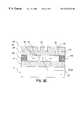
- FIG. 2 fis a cross-sectional view of the structure of a SOI MOSFET showing the relationship between the body, thick oxide, and gate regions.
- FIGS. 3 a and 3 bare circuit schematics of the SOI NMOSFET of FIG. 2 d;
- FIGS. 4 a and 4 bare circuit schematics of the SOI PMOSFET of FIG. 2 e;
- FIGS. 5 a - 5 care circuit schematics of the SOI NMOSFET of FIG. 2 d showing various coupling arrangements in accordance with a preferred embodiment of the present invention
- FIG. 6is a circuit schematic of the SOI PMOSFET of FIG. 2 e showing a body-coupled and gate-coupled arrangement in accordance with a preferred embodiment of the present invention.
- FIG. 7is an exemplary circuit schematic of an ESD protection device using the NMOSFET of FIG. 5 c and the PMOSFET of FIG. 6 .
- FIGS. 8 and 9are exemplary circuits of an ESD protection device showing different combinations of a thick oxide device with a thin oxide device.
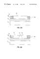
- NMOSFET device 10is shown at various stages of fabrication in accordance with a preferred embodiment of the present invention.
- NMOSFET device 10includes a semiconductor substrate layer 12 , an insulating layer 14 , and a semiconductor layer 18 .
- Semiconductor substrate layer 12is a lightly doped p-type silicon wafer.
- insulating layer 14is a silicon dioxide layer.
- the combination of semiconductor substrate layer 12 , insulating layer 14 , and semiconductor layer 18is known as the SOI structure.
- the SOI structuremay be formed by any conventional technique for fabricating SOI structures.
- the SOI structuremay be formed by implanting a high concentration of oxygen in semiconductor substrate layer 12 by a conventional separation-by-implanted-oxygen (SIMOX) technique.
- the SOI structuremay be formed by a conventional bond and etch back process.
- Field isolation regions 16 a and 16 bare formed as illustrated in FIG. 2 a . Although shallow trench isolation (STI) regions are illustrated, other field isolation processes may be used. By forming STI regions in a conventional manner, semiconductor layer 18 is separated into several islands (one is shown in FIG. 2 a ). A thin oxide layer (not shown), for example silicon dioxide, may be grown over the island of semiconductor layer 18 . The thin oxide layer may be formed by using photoresist and masking techniques known by those skilled in the art.
- STIshallow trench isolation
- a buried resistor (BR) mask(not shown) is placed over semiconductor layer 18 to subsequently form source region 20 and drain region 22 , shown in FIG. 2 b , by ion implantation through uncovered regions in the mask.
- Ion-implanting of arsenic (As)is performed at 70 KeV with a dose of about 5 ⁇ 10 15 atoms/cm 2 .
- heavily doped n+ type regions 20 and 22are formed.
- the formation of n+ regions 20 and 22is not self-aligning.
- the body region 24remains a lightly doped p-type region because the BR mask prevents ion implantation in body region 24 . Body region 24 thus forms the body between source region 20 and drain region 22 of NMOSFET 10 .
- FIG. 2 cThe next step of fabrication is shown in FIG. 2 c .
- An insulating layer 26for example silicon dioxide, is deposited over field isolation regions 16 a and 16 b , source region 20 , drain region 22 , and body region 24 .
- Insulating layer 26may be formed as an inter-level dielectric during the back-end-of-the-line (BEOL) fabrication process. Insulating layer 26 may range in thickness between about 2,000 to 3,000 ⁇ and may have a preferred thickness of approximately 2,500 ⁇ .
- BEOLback-end-of-the-line
- contact holes or vias 19are formed by etching down to source region 20 and drain region 22 , as shown in FIG. 2 c .
- metal leadsare deposited to form source lead 28 , drain lead 32 , and gate lead 30 , as shown in FIG. 2 d .
- the formation of vias 19 and the metal leadsis accomplished in a conventional manner during the BEOL fabrication process.
- body lead 25is formed as a conventional T-type structure with a metal contact to body region 24 .
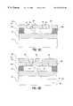
- a thick-oxide PMOSFET 40is formed from a SOI structure having a semiconductor substrate layer 12 ; an insulating layer 14 ; field isolation regions 16 a and 16 b ; heavily doped p+ type source region 20 and drain region 22 ; lightly doped n-type body region 24 ; and a thick oxide layer above body region 24 to form insulating layer 26 .
- metal leadsare deposited to form source lead 28 , drain lead 32 , gate lead 30 , and body lead 25 .
- the gateconsists of a metal film and the insulator is the BEOL Inter-Level Dielectric (ILD).
- ILDInter-Level Dielectric
- a polysilicon layermay be deposited over the SOI structure, masked, and etched to define the gate region before the deposition of the thick oxide insulator. After deposition of the thick oxide insulator, the metallization process may be performed to define the contacts to the various regions.
- the thick oxide NMOSFET of FIG. 2 dis shown as a circuit schematic in FIG. 3 a .
- thick oxide NMOSFET 10comprises source lead 28 , drain lead 32 , body lead 25 , and gate lead 30 .
- Source lead 28is connected to terminal B; drain lead 32 is connected to terminal A; body lead 25 is connected to V B ; and gate lead 30 is connected to V g .
- NMOSFET 10may be represented by the diode symbol, as shown in FIG. 3 b.
- thick oxide PMOSFET of FIG. 2 eis shown as a circuit schematic in FIG. 4 a .
- thick oxide PMOSFET 40comprises source lead 28 , drain lead 32 , body lead 25 , and gate lead 30 .
- PMOSFET 40may be represented by the diode symbol, as shown in FIG. 4 b.
- a first turn-on conditionoccurs when the body of NMOSFET 10 is subjected to a voltage which exceeds the voltage at the source of NMOSFET 10 .
- a forward-biased diode attributeallows a current flow from the body terminal to the source terminal.
- a second turn-on conditionoccurs when the voltage at the gate of NMOSFET 10 exceeds the threshold voltage of NMOSFET 10 .
- a turned-on transistor attributeallows current flow from the drain terminal to the source terminal.
- a forward-biased diode attributeallows current flow from the body terminal to the drain terminal of PMOSFET 40 .
- a second turn-on conditionoccurs when the voltage at the gate terminal of PMOSFET 40 is lower then the threshold voltage of PMSOFET 40 . When this condition occurs, a turned-on transistor attribute allows current to flow from the source terminal to the drain terminal.
- FIGS. 5 a - 5 cillustrate using the thick oxide NMOSFET 10 as described above in a variety of ESD applications in accordance with an embodiment of the present invention.
- NMOSFET 10has its body lead 25 connected to its drain lead 32 at terminal A. Terminal A is connected to pad 34 and source lead 28 is connected to V SS (usually at ground potential) at terminal B; the gate lead 30 is not connected.
- thick oxide NMOSFET 10is body-coupled to the drain terminal and provides ESD protection when the voltage at pad 34 increases above the diode forward-biased voltage existing between the body and the source terminals.
- FIG. 5 billustrates the thick oxide NMOSFET 10 in a gate-coupled arrangement.
- NMOSFET 10has its gate lead 30 connected to its drain lead 32 at terminal A. Terminal A is connected to pad 34 and source lead 28 is connected to V SS at terminal B; body lead 25 is not connected.
- thick oxide NMOSFET 10is gate-coupled to the drain terminal and provides ESD protection when the voltage at pad 34 increases above the threshold voltage of NMOSFET 10 . When the voltage at pad 34 exceeds the threshold voltage, current flows from the pad to the V SS supply.
- FIG. 5 cillustrates the thick oxide NMOSFET 10 in a body-and gate-coupled arrangement.
- NMOSFET 10has its gate lead 30 and body lead 25 connected to terminal A. Terminal A is connected to pad 34 and source lead 28 is connected to V SS at terminal B.
- thick oxide NMOSFET 10provides ESD protection at a first turn-on condition and a second turn-on condition, as described previously.
- NMOSFET 10 in a body-and gate-coupled arrangementoperates as follows. When a positive voltage is applied to pad 34 , current is discharged through the p-n diode formed by the body and source. In parallel, as the body voltage increases, the threshold voltage of NMOSFET 10 decreases, creating a dynamic threshold. As the threshold voltage decreases, the gate-coupling of the NMOSFET turns on the NMOSFET in parallel with the diode. This is a unique aspect of the body-and-gate-coupled device as it has parallel operations of a diode attribute and a transistor attribute. NMOSFET 10 uses body-coupling to lower the absolute value of the threshold voltage and gate-coupling to turn on the transistor element prior to snapback.
- the body-and-gate coupling of NMOSFET 10may be conceptually treated as a bipolar transistor with large current gain.
- the drain currentmay be modeled as the collector current, the body (gate) current as the base current, and the source current may be the emitter current.
- this devicemay be treated as a bipolar device, it is indeed a NMOSFET because the current conduction is through the surface channel and is controlled by the gate.
- the “apparent” gain of the “bipolar” deviceis large, because the threshold voltage of the NMOSFET is being modulated by the applied bias to the silicon film. This gives the appearance of large bipolar gain at low biases.
- the threshold voltage of the NMOSFETmay be controlled with the dimensions of the channel. A smaller length channel has a smaller threshold voltage. By changing the threshold-adjust implants (conventional implants that are used to control the threshold voltage), the threshold voltage may easily be changed.
- FIG. 6illustrates PMOSFET 40 configured as a body-and-gate-coupled device.
- body lead 25 , gate lead 30 , and drain lead 32are connected at terminal A.
- Source lead 28is connected to V SS at terminal B and terminal A is connected to pad 34 .
- FIG. 7illustrates NMOSFET 10 and PMOSFET 40 operating together in a first stage ESD protection device 50 .
- NMOSFET 10is coupled to V DD at terminal B and to pad 34 at terminal A.
- PMOSFET 40is coupled to V SS at terminal B and to pad 34 at terminal A.
- V DDis a predetermined high voltage supply, for example 3.4 V
- V SSis a predetermined low voltage supply, for example ground voltage.
- second stage ESD protection device 60may be added onto first stage ESD protection device 50 when mixed voltage interfacing is involved.
- the first stageis connected between the signal pad and the subsequent stage and protects against ESD events having voltages above V DD and below V SS .
- Second stage 60is connected between first stage 50 and perhaps yet another stage (not shown) and protects against an ESD event having voltages above V EE (for example 4.1 volts) and below V SS .
- signal output 62is clamped between 4.1 volts (for example) and the ground voltage of zero volts (for example).
- first stage ESD protection device 50shown in FIG. 7, may be comprised of two NMOSFETs, two PMOSFETs, or one NMOSFET and one PMOSFET.
- first stage ESD protection device 50shown in FIG. 7, may be comprised of two NMOSFETs, two PMOSFETs, or one NMOSFET and one PMOSFET.
- several stages of various element combinationsmay be used.
- Assaderaghi et al.disclose various combinations of ESD protection networks in the '857 patent; those combinations are incorporated herein by reference.
- FIG. 8shows another combination of elements.
- first stage protection device 50is comprised of a thick oxide NMOSFET 10 and a thick oxide PMOSFET 40 .
- the second stage protection device 60is comprised of a thin oxide NMOSFET 66 and a thin oxide PMOSFET 68 .
- the second stageis coupled to the first stage by a series resistor 64 .
- FIG. 9shows another embodiment having a thick oxide transistor 70 providing ESD protection.
- the thick oxide transistor 70is connected to a first stage, the first stage including a thin oxide NMOSFET 66 and a thin oxide PMOSFET 68 .
- the body and gate of thick oxide transistor 70are connected to V SS (or a ground reference potential and are not connected to either the source or the drain of transistor 70 .
- the transistoris not body and gate coupled.
Landscapes
- Semiconductor Integrated Circuits (AREA)
- Thin Film Transistor (AREA)
- Metal-Oxide And Bipolar Metal-Oxide Semiconductor Integrated Circuits (AREA)
Abstract
Description
Claims (15)
Priority Applications (7)
| Application Number | Priority Date | Filing Date | Title |
|---|---|---|---|
| US09/227,695US6323522B1 (en) | 1999-01-08 | 1999-01-08 | Silicon on insulator thick oxide structure and process of manufacture |
| SG9906260ASG83758A1 (en) | 1999-01-08 | 1999-12-09 | Silicon on insulator thick oxide structure and process of manufacture |
| CNB991261062ACN1152436C (en) | 1999-01-08 | 1999-12-10 | Insulator-base silicon thick-oxide structure and mfg. method thereof |
| TW088122779ATW457585B (en) | 1999-01-08 | 1999-12-23 | Silicon on insulator thick oxide structure and process of manufacture |
| JP37312699AJP3537035B2 (en) | 1999-01-08 | 1999-12-28 | Silicon-on-insulator network |
| KR1020000000188AKR100351648B1 (en) | 1999-01-08 | 2000-01-04 | Silicon on insulator thick oxide structure and process of manufacture |
| US09/903,820US6426244B2 (en) | 1999-01-08 | 2001-07-12 | Process of forming a thick oxide field effect transistor |
Applications Claiming Priority (1)
| Application Number | Priority Date | Filing Date | Title |
|---|---|---|---|
| US09/227,695US6323522B1 (en) | 1999-01-08 | 1999-01-08 | Silicon on insulator thick oxide structure and process of manufacture |
Related Child Applications (1)
| Application Number | Title | Priority Date | Filing Date |
|---|---|---|---|
| US09/903,820DivisionUS6426244B2 (en) | 1999-01-08 | 2001-07-12 | Process of forming a thick oxide field effect transistor |
Publications (1)
| Publication Number | Publication Date |
|---|---|
| US6323522B1true US6323522B1 (en) | 2001-11-27 |
Family
ID=22854114
Family Applications (2)
| Application Number | Title | Priority Date | Filing Date |
|---|---|---|---|
| US09/227,695Expired - LifetimeUS6323522B1 (en) | 1999-01-08 | 1999-01-08 | Silicon on insulator thick oxide structure and process of manufacture |
| US09/903,820Expired - Fee RelatedUS6426244B2 (en) | 1999-01-08 | 2001-07-12 | Process of forming a thick oxide field effect transistor |
Family Applications After (1)
| Application Number | Title | Priority Date | Filing Date |
|---|---|---|---|
| US09/903,820Expired - Fee RelatedUS6426244B2 (en) | 1999-01-08 | 2001-07-12 | Process of forming a thick oxide field effect transistor |
Country Status (6)
| Country | Link |
|---|---|
| US (2) | US6323522B1 (en) |
| JP (1) | JP3537035B2 (en) |
| KR (1) | KR100351648B1 (en) |
| CN (1) | CN1152436C (en) |
| SG (1) | SG83758A1 (en) |
| TW (1) | TW457585B (en) |
Cited By (5)
| Publication number | Priority date | Publication date | Assignee | Title |
|---|---|---|---|---|
| US6414335B1 (en)* | 2001-05-23 | 2002-07-02 | Advanced Micro Devices, Inc. | Selective state change analysis of a SOI die |
| US20020119627A1 (en)* | 2000-03-02 | 2002-08-29 | Oki Electric Industry Co., Ltd | Semiconductor device and method of manufacturing the same |
| US6621288B1 (en)* | 2001-05-23 | 2003-09-16 | Advanced Micro Devices, Inc. | Timing margin alteration via the insulator of a SOI die |
| US20050242399A1 (en)* | 2004-04-28 | 2005-11-03 | Taiwan Semiconductor Manufacturing Co., Ltd. | MOSFET with electrostatic discharge protection structure and method of fabrication |
| US20120194263A1 (en)* | 2011-01-28 | 2012-08-02 | Taiwan Semiconductor Manufacturing Company, Ltd. | Charge pump and method of biasing deep n-well in charge pump |
Families Citing this family (8)
| Publication number | Priority date | Publication date | Assignee | Title |
|---|---|---|---|---|
| JP2002305254A (en)* | 2001-04-05 | 2002-10-18 | Mitsubishi Electric Corp | Semiconductor device and manufacturing method thereof |
| US7084462B1 (en)* | 2005-04-15 | 2006-08-01 | International Business Machines Corporation | Parallel field effect transistor structure having a body contact |
| JP5586819B2 (en)* | 2006-04-06 | 2014-09-10 | ピーエスフォー ルクスコ エスエイアールエル | Semiconductor device |
| US20080246062A1 (en)* | 2007-03-26 | 2008-10-09 | Elizabeth Brauer | Semiconductor based controllable high resistance device |
| US8208233B2 (en)* | 2008-03-18 | 2012-06-26 | Mediatek Inc. | ESD protection circuit and method thereof |
| US8669146B2 (en) | 2011-01-13 | 2014-03-11 | International Business Machines Corporation | Semiconductor structures with thinned junctions and methods of manufacture |
| US8749223B2 (en)* | 2011-06-22 | 2014-06-10 | Nxp B.V. | Galvanic isolation device and method |
| CN117176098A (en)* | 2023-11-01 | 2023-12-05 | 上海安其威微电子科技有限公司 | Amplitude limiting circuit and wireless transceiver |
Citations (20)
| Publication number | Priority date | Publication date | Assignee | Title |
|---|---|---|---|---|
| US4115709A (en) | 1974-07-16 | 1978-09-19 | Nippon Electric Co., Ltd. | Gate controlled diode protection for drain of IGFET |
| US4408245A (en) | 1981-12-28 | 1983-10-04 | Rca Corporation | Protection and anti-floating network for insulated-gate field-effect circuitry |
| US4626882A (en) | 1984-07-18 | 1986-12-02 | International Business Machines Corporation | Twin diode overvoltage protection structure |
| US4889829A (en) | 1988-01-18 | 1989-12-26 | Fujitsu Limited | Method for producing a semiconductor device having a silicon-on-insulator structure |
| US4946799A (en) | 1988-07-08 | 1990-08-07 | Texas Instruments, Incorporated | Process for making high performance silicon-on-insulator transistor with body node to source node connection |
| US4989057A (en) | 1988-05-26 | 1991-01-29 | Texas Instruments Incorporated | ESD protection for SOI circuits |
| US5023692A (en) | 1989-12-07 | 1991-06-11 | Harris Semiconductor Patents, Inc. | Power MOSFET transistor circuit |
| US5144390A (en) | 1988-09-02 | 1992-09-01 | Texas Instruments Incorporated | Silicon-on insulator transistor with internal body node to source node connection |
| US5159518A (en) | 1990-01-17 | 1992-10-27 | Vlsi Technology, Inc. | Input protection circuit for CMOS devices |
| US5204988A (en) | 1990-07-16 | 1993-04-20 | Fuji Electic Co., Ltd. | Mos semiconductor device having a surge protecting element |
| US5382818A (en) | 1993-12-08 | 1995-01-17 | Philips Electronics North America Corporation | Lateral semiconductor-on-insulator (SOI) semiconductor device having a buried diode |
| US5401996A (en) | 1991-07-19 | 1995-03-28 | U.S. Philips Corporation | Overvoltage protected semiconductor switch |
| US5597747A (en)* | 1995-12-15 | 1997-01-28 | Industrial Technology Research Institute | Method of making inverted thin film transistor using backsick exposure and negative photoresist |
| US5683918A (en) | 1996-04-01 | 1997-11-04 | Motorola, Inc. | Method of making semiconductor-on-insulator device with closed-gate electrode |
| US5708288A (en) | 1995-11-02 | 1998-01-13 | Motorola, Inc. | Thin film silicon on insulator semiconductor integrated circuit with electrostatic damage protection and method |
| US5726844A (en) | 1996-04-01 | 1998-03-10 | Motorola, Inc. | Protection circuit and a circuit for a semiconductor-on-insulator device |
| US5760444A (en) | 1995-05-31 | 1998-06-02 | Nec Corporation | Silicon on insulator type semiconductor device |
| US5773326A (en) | 1996-09-19 | 1998-06-30 | Motorola, Inc. | Method of making an SOI integrated circuit with ESD protection |
| US5811857A (en) | 1996-10-22 | 1998-09-22 | International Business Machines Corporation | Silicon-on-insulator body-coupled gated diode for electrostatic discharge (ESD) and analog applications |
| US5845561A (en)* | 1996-04-17 | 1998-12-08 | Sanyo Electric Co., Ltd. | Apparatus for preparing a coffee beverage |
Family Cites Families (6)
| Publication number | Priority date | Publication date | Assignee | Title |
|---|---|---|---|---|
| JPS6048106B2 (en)* | 1979-12-24 | 1985-10-25 | 富士通株式会社 | semiconductor integrated circuit |
| US5436183A (en)* | 1990-04-17 | 1995-07-25 | National Semiconductor Corporation | Electrostatic discharge protection transistor element fabrication process |
| JP3405364B2 (en)* | 1993-03-08 | 2003-05-12 | セイコーインスツルメンツ株式会社 | Semiconductor device |
| KR0169157B1 (en) | 1993-11-29 | 1999-02-01 | 기다오까 다까시 | Semiconductor circuit and mos-dram |
| US5489792A (en)* | 1994-04-07 | 1996-02-06 | Regents Of The University Of California | Silicon-on-insulator transistors having improved current characteristics and reduced electrostatic discharge susceptibility |
| US5952695A (en)* | 1997-03-05 | 1999-09-14 | International Business Machines Corporation | Silicon-on-insulator and CMOS-on-SOI double film structures |
- 1999
- 1999-01-08USUS09/227,695patent/US6323522B1/ennot_activeExpired - Lifetime
- 1999-12-09SGSG9906260Apatent/SG83758A1/enunknown
- 1999-12-10CNCNB991261062Apatent/CN1152436C/ennot_activeExpired - Lifetime
- 1999-12-23TWTW088122779Apatent/TW457585B/ennot_activeIP Right Cessation
- 1999-12-28JPJP37312699Apatent/JP3537035B2/ennot_activeExpired - Fee Related
- 2000
- 2000-01-04KRKR1020000000188Apatent/KR100351648B1/ennot_activeExpired - Fee Related
- 2001
- 2001-07-12USUS09/903,820patent/US6426244B2/ennot_activeExpired - Fee Related
Patent Citations (20)
| Publication number | Priority date | Publication date | Assignee | Title |
|---|---|---|---|---|
| US4115709A (en) | 1974-07-16 | 1978-09-19 | Nippon Electric Co., Ltd. | Gate controlled diode protection for drain of IGFET |
| US4408245A (en) | 1981-12-28 | 1983-10-04 | Rca Corporation | Protection and anti-floating network for insulated-gate field-effect circuitry |
| US4626882A (en) | 1984-07-18 | 1986-12-02 | International Business Machines Corporation | Twin diode overvoltage protection structure |
| US4889829A (en) | 1988-01-18 | 1989-12-26 | Fujitsu Limited | Method for producing a semiconductor device having a silicon-on-insulator structure |
| US4989057A (en) | 1988-05-26 | 1991-01-29 | Texas Instruments Incorporated | ESD protection for SOI circuits |
| US4946799A (en) | 1988-07-08 | 1990-08-07 | Texas Instruments, Incorporated | Process for making high performance silicon-on-insulator transistor with body node to source node connection |
| US5144390A (en) | 1988-09-02 | 1992-09-01 | Texas Instruments Incorporated | Silicon-on insulator transistor with internal body node to source node connection |
| US5023692A (en) | 1989-12-07 | 1991-06-11 | Harris Semiconductor Patents, Inc. | Power MOSFET transistor circuit |
| US5159518A (en) | 1990-01-17 | 1992-10-27 | Vlsi Technology, Inc. | Input protection circuit for CMOS devices |
| US5204988A (en) | 1990-07-16 | 1993-04-20 | Fuji Electic Co., Ltd. | Mos semiconductor device having a surge protecting element |
| US5401996A (en) | 1991-07-19 | 1995-03-28 | U.S. Philips Corporation | Overvoltage protected semiconductor switch |
| US5382818A (en) | 1993-12-08 | 1995-01-17 | Philips Electronics North America Corporation | Lateral semiconductor-on-insulator (SOI) semiconductor device having a buried diode |
| US5760444A (en) | 1995-05-31 | 1998-06-02 | Nec Corporation | Silicon on insulator type semiconductor device |
| US5708288A (en) | 1995-11-02 | 1998-01-13 | Motorola, Inc. | Thin film silicon on insulator semiconductor integrated circuit with electrostatic damage protection and method |
| US5597747A (en)* | 1995-12-15 | 1997-01-28 | Industrial Technology Research Institute | Method of making inverted thin film transistor using backsick exposure and negative photoresist |
| US5683918A (en) | 1996-04-01 | 1997-11-04 | Motorola, Inc. | Method of making semiconductor-on-insulator device with closed-gate electrode |
| US5726844A (en) | 1996-04-01 | 1998-03-10 | Motorola, Inc. | Protection circuit and a circuit for a semiconductor-on-insulator device |
| US5845561A (en)* | 1996-04-17 | 1998-12-08 | Sanyo Electric Co., Ltd. | Apparatus for preparing a coffee beverage |
| US5773326A (en) | 1996-09-19 | 1998-06-30 | Motorola, Inc. | Method of making an SOI integrated circuit with ESD protection |
| US5811857A (en) | 1996-10-22 | 1998-09-22 | International Business Machines Corporation | Silicon-on-insulator body-coupled gated diode for electrostatic discharge (ESD) and analog applications |
Non-Patent Citations (1)
| Title |
|---|
| Remshardt, et al, "Surface Controlled Semiconductor Arrangement" IBM Technical Disclosure Bulletin, Vol. 14, No. 5, Feb. 1972, p. 2592. |
Cited By (9)
| Publication number | Priority date | Publication date | Assignee | Title |
|---|---|---|---|---|
| US20020119627A1 (en)* | 2000-03-02 | 2002-08-29 | Oki Electric Industry Co., Ltd | Semiconductor device and method of manufacturing the same |
| US6806538B2 (en)* | 2000-03-02 | 2004-10-19 | Oki Electric Industry Co., Ltd. | SOI semiconductor device |
| US6414335B1 (en)* | 2001-05-23 | 2002-07-02 | Advanced Micro Devices, Inc. | Selective state change analysis of a SOI die |
| US6621288B1 (en)* | 2001-05-23 | 2003-09-16 | Advanced Micro Devices, Inc. | Timing margin alteration via the insulator of a SOI die |
| US20050242399A1 (en)* | 2004-04-28 | 2005-11-03 | Taiwan Semiconductor Manufacturing Co., Ltd. | MOSFET with electrostatic discharge protection structure and method of fabrication |
| US7166876B2 (en)* | 2004-04-28 | 2007-01-23 | Taiwan Semiconductor Manufacturing Company, Ltd. | MOSFET with electrostatic discharge protection structure and method of fabrication |
| US20120194263A1 (en)* | 2011-01-28 | 2012-08-02 | Taiwan Semiconductor Manufacturing Company, Ltd. | Charge pump and method of biasing deep n-well in charge pump |
| US8710908B2 (en)* | 2011-01-28 | 2014-04-29 | Taiwan Semiconductor Manufacturing Company, Ltd. | Charge pump and method of biasing deep N-well in charge pump |
| US9054577B2 (en) | 2011-01-28 | 2015-06-09 | Taiwan Semiconductor Manufacturing Company, Ltd. | Charge pump and method of biasing deep N-well in charge pump |
Also Published As
| Publication number | Publication date |
|---|---|
| CN1152436C (en) | 2004-06-02 |
| KR100351648B1 (en) | 2002-09-11 |
| TW457585B (en) | 2001-10-01 |
| JP2000208779A (en) | 2000-07-28 |
| US6426244B2 (en) | 2002-07-30 |
| US20010041393A1 (en) | 2001-11-15 |
| KR20000053384A (en) | 2000-08-25 |
| SG83758A1 (en) | 2001-10-16 |
| CN1260597A (en) | 2000-07-19 |
| JP3537035B2 (en) | 2004-06-14 |
Similar Documents
| Publication | Publication Date | Title |
|---|---|---|
| US7285458B2 (en) | Method for forming an ESD protection circuit | |
| KR100325553B1 (en) | Electrostatic discharge protection device for semiconductor integrated circuit, method for producing the same, and electrostatic discharge protection circuit using the same | |
| US6909149B2 (en) | Low voltage silicon controlled rectifier (SCR) for electrostatic discharge (ESD) protection of silicon-on-insulator technologies | |
| US6653709B2 (en) | CMOS output circuit with enhanced ESD protection using drain side implantation | |
| US4893157A (en) | Semiconductor device | |
| US6879003B1 (en) | Electrostatic discharge (ESD) protection MOS device and ESD circuitry thereof | |
| US20050212051A1 (en) | Low voltage silicon controlled rectifier (SCR) for electrostatic discharge (ESD) protection of silicon-on-insulator technologies | |
| JP3090081B2 (en) | Semiconductor device | |
| JPH10504424A (en) | Electrostatic discharge protection circuit | |
| JPH06196634A (en) | Depletion control type separation stage | |
| US6323522B1 (en) | Silicon on insulator thick oxide structure and process of manufacture | |
| US5604655A (en) | Semiconductor protection circuit and semiconductor protection device | |
| US7462885B2 (en) | ESD structure for high voltage ESD protection | |
| KR20060050160A (en) | Semiconductor integrated circuit device | |
| EP0538752B1 (en) | Semiconductor input protective device against external surge voltage | |
| US6063672A (en) | NMOS electrostatic discharge protection device and method for CMOS integrated circuit | |
| US20060125054A1 (en) | Electrostatic discharge protection circuit using zener triggered silicon controlled rectifier | |
| US7342281B2 (en) | Electrostatic discharge protection circuit using triple welled silicon controlled rectifier | |
| US6894320B2 (en) | Input protection circuit | |
| EP0772238A2 (en) | Semiconductor device with protecting means | |
| US20060157791A1 (en) | ESD protection device | |
| KR100247840B1 (en) | Soi type semiconductor device | |
| US6455895B1 (en) | Overvoltage protector having same gate thickness as the protected integrated circuit | |
| JP3425574B2 (en) | Input/output protection device for semiconductor integrated circuits | |
| KR100591125B1 (en) | Gate Ground EnMOS Transistor for Protection from Electrostatic Discharge |
Legal Events
| Date | Code | Title | Description |
|---|---|---|---|
| AS | Assignment | Owner name:INTERNATIONAL BUSINESS MACHINES CORPORATION, NEW Y Free format text:ASSIGNMENT OF ASSIGNORS INTEREST;ASSIGNORS:HARGROVE, MICHAEL J.;PELELLA, MARIO M.;VOLDMAN, STEVEN H.;REEL/FRAME:009702/0986;SIGNING DATES FROM 19981116 TO 19981204 | |
| STCF | Information on status: patent grant | Free format text:PATENTED CASE | |
| CC | Certificate of correction | ||
| FPAY | Fee payment | Year of fee payment:4 | |
| FPAY | Fee payment | Year of fee payment:8 | |
| FPAY | Fee payment | Year of fee payment:12 | |
| AS | Assignment | Owner name:GLOBALFOUNDRIES U.S. 2 LLC, NEW YORK Free format text:ASSIGNMENT OF ASSIGNORS INTEREST;ASSIGNOR:INTERNATIONAL BUSINESS MACHINES CORPORATION;REEL/FRAME:036550/0001 Effective date:20150629 | |
| AS | Assignment | Owner name:GLOBALFOUNDRIES INC., CAYMAN ISLANDS Free format text:ASSIGNMENT OF ASSIGNORS INTEREST;ASSIGNORS:GLOBALFOUNDRIES U.S. 2 LLC;GLOBALFOUNDRIES U.S. INC.;REEL/FRAME:036779/0001 Effective date:20150910 | |
| AS | Assignment | Owner name:WILMINGTON TRUST, NATIONAL ASSOCIATION, DELAWARE Free format text:SECURITY AGREEMENT;ASSIGNOR:GLOBALFOUNDRIES INC.;REEL/FRAME:049490/0001 Effective date:20181127 | |
| AS | Assignment | Owner name:GLOBALFOUNDRIES INC., CAYMAN ISLANDS Free format text:RELEASE BY SECURED PARTY;ASSIGNOR:WILMINGTON TRUST, NATIONAL ASSOCIATION;REEL/FRAME:054636/0001 Effective date:20201117 | |
| AS | Assignment | Owner name:GLOBALFOUNDRIES U.S. INC., NEW YORK Free format text:RELEASE BY SECURED PARTY;ASSIGNOR:WILMINGTON TRUST, NATIONAL ASSOCIATION;REEL/FRAME:056987/0001 Effective date:20201117 |