US6322903B1 - Package of integrated circuits and vertical integration - Google Patents
Package of integrated circuits and vertical integrationDownload PDFInfo
- Publication number
- US6322903B1 US6322903B1US09/456,225US45622599AUS6322903B1US 6322903 B1US6322903 B1US 6322903B1US 45622599 AUS45622599 AUS 45622599AUS 6322903 B1US6322903 B1US 6322903B1
- Authority
- US
- United States
- Prior art keywords
- substrate
- wafer
- contact
- bonding
- vias
- Prior art date
- Legal status (The legal status is an assumption and is not a legal conclusion. Google has not performed a legal analysis and makes no representation as to the accuracy of the status listed.)
- Expired - Lifetime
Links
Images


Classifications
- H—ELECTRICITY
- H01—ELECTRIC ELEMENTS
- H01L—SEMICONDUCTOR DEVICES NOT COVERED BY CLASS H10
- H01L25/00—Assemblies consisting of a plurality of semiconductor or other solid state devices
- H01L25/50—Multistep manufacturing processes of assemblies consisting of devices, the devices being individual devices of subclass H10D or integrated devices of class H10
- H—ELECTRICITY
- H01—ELECTRIC ELEMENTS
- H01L—SEMICONDUCTOR DEVICES NOT COVERED BY CLASS H10
- H01L21/00—Processes or apparatus adapted for the manufacture or treatment of semiconductor or solid state devices or of parts thereof
- H01L21/67—Apparatus specially adapted for handling semiconductor or electric solid state devices during manufacture or treatment thereof; Apparatus specially adapted for handling wafers during manufacture or treatment of semiconductor or electric solid state devices or components ; Apparatus not specifically provided for elsewhere
- H01L21/683—Apparatus specially adapted for handling semiconductor or electric solid state devices during manufacture or treatment thereof; Apparatus specially adapted for handling wafers during manufacture or treatment of semiconductor or electric solid state devices or components ; Apparatus not specifically provided for elsewhere for supporting or gripping
- H01L21/6835—Apparatus specially adapted for handling semiconductor or electric solid state devices during manufacture or treatment thereof; Apparatus specially adapted for handling wafers during manufacture or treatment of semiconductor or electric solid state devices or components ; Apparatus not specifically provided for elsewhere for supporting or gripping using temporarily an auxiliary support
- H—ELECTRICITY
- H01—ELECTRIC ELEMENTS
- H01L—SEMICONDUCTOR DEVICES NOT COVERED BY CLASS H10
- H01L21/00—Processes or apparatus adapted for the manufacture or treatment of semiconductor or solid state devices or of parts thereof
- H01L21/70—Manufacture or treatment of devices consisting of a plurality of solid state components formed in or on a common substrate or of parts thereof; Manufacture of integrated circuit devices or of parts thereof
- H01L21/71—Manufacture of specific parts of devices defined in group H01L21/70
- H01L21/768—Applying interconnections to be used for carrying current between separate components within a device comprising conductors and dielectrics
- H01L21/76898—Applying interconnections to be used for carrying current between separate components within a device comprising conductors and dielectrics formed through a semiconductor substrate
- H—ELECTRICITY
- H01—ELECTRIC ELEMENTS
- H01L—SEMICONDUCTOR DEVICES NOT COVERED BY CLASS H10
- H01L23/00—Details of semiconductor or other solid state devices
- H01L23/48—Arrangements for conducting electric current to or from the solid state body in operation, e.g. leads, terminal arrangements ; Selection of materials therefor
- H01L23/481—Internal lead connections, e.g. via connections, feedthrough structures
- H—ELECTRICITY
- H01—ELECTRIC ELEMENTS
- H01L—SEMICONDUCTOR DEVICES NOT COVERED BY CLASS H10
- H01L24/00—Arrangements for connecting or disconnecting semiconductor or solid-state bodies; Methods or apparatus related thereto
- H01L24/01—Means for bonding being attached to, or being formed on, the surface to be connected, e.g. chip-to-package, die-attach, "first-level" interconnects; Manufacturing methods related thereto
- H01L24/10—Bump connectors ; Manufacturing methods related thereto
- H01L24/11—Manufacturing methods
- H—ELECTRICITY
- H01—ELECTRIC ELEMENTS
- H01L—SEMICONDUCTOR DEVICES NOT COVERED BY CLASS H10
- H01L24/00—Arrangements for connecting or disconnecting semiconductor or solid-state bodies; Methods or apparatus related thereto
- H01L24/01—Means for bonding being attached to, or being formed on, the surface to be connected, e.g. chip-to-package, die-attach, "first-level" interconnects; Manufacturing methods related thereto
- H01L24/10—Bump connectors ; Manufacturing methods related thereto
- H01L24/12—Structure, shape, material or disposition of the bump connectors prior to the connecting process
- H01L24/13—Structure, shape, material or disposition of the bump connectors prior to the connecting process of an individual bump connector
- H—ELECTRICITY
- H01—ELECTRIC ELEMENTS
- H01L—SEMICONDUCTOR DEVICES NOT COVERED BY CLASS H10
- H01L24/00—Arrangements for connecting or disconnecting semiconductor or solid-state bodies; Methods or apparatus related thereto
- H01L24/80—Methods for connecting semiconductor or other solid state bodies using means for bonding being attached to, or being formed on, the surface to be connected
- H01L24/81—Methods for connecting semiconductor or other solid state bodies using means for bonding being attached to, or being formed on, the surface to be connected using a bump connector
- H—ELECTRICITY
- H01—ELECTRIC ELEMENTS
- H01L—SEMICONDUCTOR DEVICES NOT COVERED BY CLASS H10
- H01L25/00—Assemblies consisting of a plurality of semiconductor or other solid state devices
- H01L25/03—Assemblies consisting of a plurality of semiconductor or other solid state devices all the devices being of a type provided for in a single subclass of subclasses H10B, H10D, H10F, H10H, H10K or H10N, e.g. assemblies of rectifier diodes
- H01L25/04—Assemblies consisting of a plurality of semiconductor or other solid state devices all the devices being of a type provided for in a single subclass of subclasses H10B, H10D, H10F, H10H, H10K or H10N, e.g. assemblies of rectifier diodes the devices not having separate containers
- H01L25/065—Assemblies consisting of a plurality of semiconductor or other solid state devices all the devices being of a type provided for in a single subclass of subclasses H10B, H10D, H10F, H10H, H10K or H10N, e.g. assemblies of rectifier diodes the devices not having separate containers the devices being of a type provided for in group H10D89/00
- H01L25/0657—Stacked arrangements of devices
- H—ELECTRICITY
- H01—ELECTRIC ELEMENTS
- H01L—SEMICONDUCTOR DEVICES NOT COVERED BY CLASS H10
- H01L2221/00—Processes or apparatus adapted for the manufacture or treatment of semiconductor or solid state devices or of parts thereof covered by H01L21/00
- H01L2221/67—Apparatus for handling semiconductor or electric solid state devices during manufacture or treatment thereof; Apparatus for handling wafers during manufacture or treatment of semiconductor or electric solid state devices or components; Apparatus not specifically provided for elsewhere
- H01L2221/683—Apparatus for handling semiconductor or electric solid state devices during manufacture or treatment thereof; Apparatus for handling wafers during manufacture or treatment of semiconductor or electric solid state devices or components; Apparatus not specifically provided for elsewhere for supporting or gripping
- H01L2221/68304—Apparatus for handling semiconductor or electric solid state devices during manufacture or treatment thereof; Apparatus for handling wafers during manufacture or treatment of semiconductor or electric solid state devices or components; Apparatus not specifically provided for elsewhere for supporting or gripping using temporarily an auxiliary support
- H01L2221/68359—Apparatus for handling semiconductor or electric solid state devices during manufacture or treatment thereof; Apparatus for handling wafers during manufacture or treatment of semiconductor or electric solid state devices or components; Apparatus not specifically provided for elsewhere for supporting or gripping using temporarily an auxiliary support used as a support during manufacture of interconnect decals or build up layers
- H—ELECTRICITY
- H01—ELECTRIC ELEMENTS
- H01L—SEMICONDUCTOR DEVICES NOT COVERED BY CLASS H10
- H01L2221/00—Processes or apparatus adapted for the manufacture or treatment of semiconductor or solid state devices or of parts thereof covered by H01L21/00
- H01L2221/67—Apparatus for handling semiconductor or electric solid state devices during manufacture or treatment thereof; Apparatus for handling wafers during manufacture or treatment of semiconductor or electric solid state devices or components; Apparatus not specifically provided for elsewhere
- H01L2221/683—Apparatus for handling semiconductor or electric solid state devices during manufacture or treatment thereof; Apparatus for handling wafers during manufacture or treatment of semiconductor or electric solid state devices or components; Apparatus not specifically provided for elsewhere for supporting or gripping
- H01L2221/68304—Apparatus for handling semiconductor or electric solid state devices during manufacture or treatment thereof; Apparatus for handling wafers during manufacture or treatment of semiconductor or electric solid state devices or components; Apparatus not specifically provided for elsewhere for supporting or gripping using temporarily an auxiliary support
- H01L2221/68363—Apparatus for handling semiconductor or electric solid state devices during manufacture or treatment thereof; Apparatus for handling wafers during manufacture or treatment of semiconductor or electric solid state devices or components; Apparatus not specifically provided for elsewhere for supporting or gripping using temporarily an auxiliary support used in a transfer process involving transfer directly from an origin substrate to a target substrate without use of an intermediate handle substrate
- H—ELECTRICITY
- H01—ELECTRIC ELEMENTS
- H01L—SEMICONDUCTOR DEVICES NOT COVERED BY CLASS H10
- H01L2224/00—Indexing scheme for arrangements for connecting or disconnecting semiconductor or solid-state bodies and methods related thereto as covered by H01L24/00
- H01L2224/01—Means for bonding being attached to, or being formed on, the surface to be connected, e.g. chip-to-package, die-attach, "first-level" interconnects; Manufacturing methods related thereto
- H01L2224/02—Bonding areas; Manufacturing methods related thereto
- H01L2224/04—Structure, shape, material or disposition of the bonding areas prior to the connecting process
- H01L2224/0401—Bonding areas specifically adapted for bump connectors, e.g. under bump metallisation [UBM]
- H—ELECTRICITY
- H01—ELECTRIC ELEMENTS
- H01L—SEMICONDUCTOR DEVICES NOT COVERED BY CLASS H10
- H01L2224/00—Indexing scheme for arrangements for connecting or disconnecting semiconductor or solid-state bodies and methods related thereto as covered by H01L24/00
- H01L2224/01—Means for bonding being attached to, or being formed on, the surface to be connected, e.g. chip-to-package, die-attach, "first-level" interconnects; Manufacturing methods related thereto
- H01L2224/10—Bump connectors; Manufacturing methods related thereto
- H01L2224/12—Structure, shape, material or disposition of the bump connectors prior to the connecting process
- H01L2224/13—Structure, shape, material or disposition of the bump connectors prior to the connecting process of an individual bump connector
- H01L2224/13001—Core members of the bump connector
- H01L2224/13099—Material
- H01L2224/1319—Material with a principal constituent of the material being a polymer, e.g. polyester, phenolic based polymer, epoxy
- H—ELECTRICITY
- H01—ELECTRIC ELEMENTS
- H01L—SEMICONDUCTOR DEVICES NOT COVERED BY CLASS H10
- H01L2224/00—Indexing scheme for arrangements for connecting or disconnecting semiconductor or solid-state bodies and methods related thereto as covered by H01L24/00
- H01L2224/01—Means for bonding being attached to, or being formed on, the surface to be connected, e.g. chip-to-package, die-attach, "first-level" interconnects; Manufacturing methods related thereto
- H01L2224/10—Bump connectors; Manufacturing methods related thereto
- H01L2224/12—Structure, shape, material or disposition of the bump connectors prior to the connecting process
- H01L2224/13—Structure, shape, material or disposition of the bump connectors prior to the connecting process of an individual bump connector
- H01L2224/1354—Coating
- H01L2224/1357—Single coating layer
- H—ELECTRICITY
- H01—ELECTRIC ELEMENTS
- H01L—SEMICONDUCTOR DEVICES NOT COVERED BY CLASS H10
- H01L2224/00—Indexing scheme for arrangements for connecting or disconnecting semiconductor or solid-state bodies and methods related thereto as covered by H01L24/00
- H01L2224/01—Means for bonding being attached to, or being formed on, the surface to be connected, e.g. chip-to-package, die-attach, "first-level" interconnects; Manufacturing methods related thereto
- H01L2224/10—Bump connectors; Manufacturing methods related thereto
- H01L2224/12—Structure, shape, material or disposition of the bump connectors prior to the connecting process
- H01L2224/13—Structure, shape, material or disposition of the bump connectors prior to the connecting process of an individual bump connector
- H01L2224/1354—Coating
- H01L2224/13599—Material
- H01L2224/136—Material with a principal constituent of the material being a metal or a metalloid, e.g. boron [B], silicon [Si], germanium [Ge], arsenic [As], antimony [Sb], tellurium [Te] and polonium [Po], and alloys thereof
- H—ELECTRICITY
- H01—ELECTRIC ELEMENTS
- H01L—SEMICONDUCTOR DEVICES NOT COVERED BY CLASS H10
- H01L2224/00—Indexing scheme for arrangements for connecting or disconnecting semiconductor or solid-state bodies and methods related thereto as covered by H01L24/00
- H01L2224/01—Means for bonding being attached to, or being formed on, the surface to be connected, e.g. chip-to-package, die-attach, "first-level" interconnects; Manufacturing methods related thereto
- H01L2224/10—Bump connectors; Manufacturing methods related thereto
- H01L2224/15—Structure, shape, material or disposition of the bump connectors after the connecting process
- H01L2224/16—Structure, shape, material or disposition of the bump connectors after the connecting process of an individual bump connector
- H01L2224/161—Disposition
- H01L2224/16151—Disposition the bump connector connecting between a semiconductor or solid-state body and an item not being a semiconductor or solid-state body, e.g. chip-to-substrate, chip-to-passive
- H01L2224/16221—Disposition the bump connector connecting between a semiconductor or solid-state body and an item not being a semiconductor or solid-state body, e.g. chip-to-substrate, chip-to-passive the body and the item being stacked
- H01L2224/16225—Disposition the bump connector connecting between a semiconductor or solid-state body and an item not being a semiconductor or solid-state body, e.g. chip-to-substrate, chip-to-passive the body and the item being stacked the item being non-metallic, e.g. insulating substrate with or without metallisation
- H01L2224/16237—Disposition the bump connector connecting between a semiconductor or solid-state body and an item not being a semiconductor or solid-state body, e.g. chip-to-substrate, chip-to-passive the body and the item being stacked the item being non-metallic, e.g. insulating substrate with or without metallisation the bump connector connecting to a bonding area disposed in a recess of the surface of the item
- H—ELECTRICITY
- H01—ELECTRIC ELEMENTS
- H01L—SEMICONDUCTOR DEVICES NOT COVERED BY CLASS H10
- H01L2224/00—Indexing scheme for arrangements for connecting or disconnecting semiconductor or solid-state bodies and methods related thereto as covered by H01L24/00
- H01L2224/80—Methods for connecting semiconductor or other solid state bodies using means for bonding being attached to, or being formed on, the surface to be connected
- H01L2224/81—Methods for connecting semiconductor or other solid state bodies using means for bonding being attached to, or being formed on, the surface to be connected using a bump connector
- H01L2224/8119—Arrangement of the bump connectors prior to mounting
- H01L2224/81191—Arrangement of the bump connectors prior to mounting wherein the bump connectors are disposed only on the semiconductor or solid-state body
- H—ELECTRICITY
- H01—ELECTRIC ELEMENTS
- H01L—SEMICONDUCTOR DEVICES NOT COVERED BY CLASS H10
- H01L2225/00—Details relating to assemblies covered by the group H01L25/00 but not provided for in its subgroups
- H01L2225/03—All the devices being of a type provided for in the same main group of the same subclass of class H10, e.g. assemblies of rectifier diodes
- H01L2225/04—All the devices being of a type provided for in the same main group of the same subclass of class H10, e.g. assemblies of rectifier diodes the devices not having separate containers
- H01L2225/065—All the devices being of a type provided for in the same main group of the same subclass of class H10
- H01L2225/06503—Stacked arrangements of devices
- H01L2225/06513—Bump or bump-like direct electrical connections between devices, e.g. flip-chip connection, solder bumps
- H—ELECTRICITY
- H01—ELECTRIC ELEMENTS
- H01L—SEMICONDUCTOR DEVICES NOT COVERED BY CLASS H10
- H01L2225/00—Details relating to assemblies covered by the group H01L25/00 but not provided for in its subgroups
- H01L2225/03—All the devices being of a type provided for in the same main group of the same subclass of class H10, e.g. assemblies of rectifier diodes
- H01L2225/04—All the devices being of a type provided for in the same main group of the same subclass of class H10, e.g. assemblies of rectifier diodes the devices not having separate containers
- H01L2225/065—All the devices being of a type provided for in the same main group of the same subclass of class H10
- H01L2225/06503—Stacked arrangements of devices
- H01L2225/06527—Special adaptation of electrical connections, e.g. rewiring, engineering changes, pressure contacts, layout
- H—ELECTRICITY
- H01—ELECTRIC ELEMENTS
- H01L—SEMICONDUCTOR DEVICES NOT COVERED BY CLASS H10
- H01L2225/00—Details relating to assemblies covered by the group H01L25/00 but not provided for in its subgroups
- H01L2225/03—All the devices being of a type provided for in the same main group of the same subclass of class H10, e.g. assemblies of rectifier diodes
- H01L2225/04—All the devices being of a type provided for in the same main group of the same subclass of class H10, e.g. assemblies of rectifier diodes the devices not having separate containers
- H01L2225/065—All the devices being of a type provided for in the same main group of the same subclass of class H10
- H01L2225/06503—Stacked arrangements of devices
- H01L2225/06541—Conductive via connections through the device, e.g. vertical interconnects, through silicon via [TSV]
- H—ELECTRICITY
- H01—ELECTRIC ELEMENTS
- H01L—SEMICONDUCTOR DEVICES NOT COVERED BY CLASS H10
- H01L24/00—Arrangements for connecting or disconnecting semiconductor or solid-state bodies; Methods or apparatus related thereto
- H01L24/01—Means for bonding being attached to, or being formed on, the surface to be connected, e.g. chip-to-package, die-attach, "first-level" interconnects; Manufacturing methods related thereto
- H01L24/02—Bonding areas ; Manufacturing methods related thereto
- H—ELECTRICITY
- H01—ELECTRIC ELEMENTS
- H01L—SEMICONDUCTOR DEVICES NOT COVERED BY CLASS H10
- H01L24/00—Arrangements for connecting or disconnecting semiconductor or solid-state bodies; Methods or apparatus related thereto
- H01L24/01—Means for bonding being attached to, or being formed on, the surface to be connected, e.g. chip-to-package, die-attach, "first-level" interconnects; Manufacturing methods related thereto
- H01L24/10—Bump connectors ; Manufacturing methods related thereto
- H01L24/15—Structure, shape, material or disposition of the bump connectors after the connecting process
- H01L24/16—Structure, shape, material or disposition of the bump connectors after the connecting process of an individual bump connector
- H—ELECTRICITY
- H01—ELECTRIC ELEMENTS
- H01L—SEMICONDUCTOR DEVICES NOT COVERED BY CLASS H10
- H01L2924/00—Indexing scheme for arrangements or methods for connecting or disconnecting semiconductor or solid-state bodies as covered by H01L24/00
- H01L2924/0001—Technical content checked by a classifier
- H—ELECTRICITY
- H01—ELECTRIC ELEMENTS
- H01L—SEMICONDUCTOR DEVICES NOT COVERED BY CLASS H10
- H01L2924/00—Indexing scheme for arrangements or methods for connecting or disconnecting semiconductor or solid-state bodies as covered by H01L24/00
- H01L2924/01—Chemical elements
- H01L2924/01005—Boron [B]
- H—ELECTRICITY
- H01—ELECTRIC ELEMENTS
- H01L—SEMICONDUCTOR DEVICES NOT COVERED BY CLASS H10
- H01L2924/00—Indexing scheme for arrangements or methods for connecting or disconnecting semiconductor or solid-state bodies as covered by H01L24/00
- H01L2924/01—Chemical elements
- H01L2924/01006—Carbon [C]
- H—ELECTRICITY
- H01—ELECTRIC ELEMENTS
- H01L—SEMICONDUCTOR DEVICES NOT COVERED BY CLASS H10
- H01L2924/00—Indexing scheme for arrangements or methods for connecting or disconnecting semiconductor or solid-state bodies as covered by H01L24/00
- H01L2924/01—Chemical elements
- H01L2924/01013—Aluminum [Al]
- H—ELECTRICITY
- H01—ELECTRIC ELEMENTS
- H01L—SEMICONDUCTOR DEVICES NOT COVERED BY CLASS H10
- H01L2924/00—Indexing scheme for arrangements or methods for connecting or disconnecting semiconductor or solid-state bodies as covered by H01L24/00
- H01L2924/01—Chemical elements
- H01L2924/01014—Silicon [Si]
- H—ELECTRICITY
- H01—ELECTRIC ELEMENTS
- H01L—SEMICONDUCTOR DEVICES NOT COVERED BY CLASS H10
- H01L2924/00—Indexing scheme for arrangements or methods for connecting or disconnecting semiconductor or solid-state bodies as covered by H01L24/00
- H01L2924/01—Chemical elements
- H01L2924/01022—Titanium [Ti]
- H—ELECTRICITY
- H01—ELECTRIC ELEMENTS
- H01L—SEMICONDUCTOR DEVICES NOT COVERED BY CLASS H10
- H01L2924/00—Indexing scheme for arrangements or methods for connecting or disconnecting semiconductor or solid-state bodies as covered by H01L24/00
- H01L2924/01—Chemical elements
- H01L2924/01023—Vanadium [V]
- H—ELECTRICITY
- H01—ELECTRIC ELEMENTS
- H01L—SEMICONDUCTOR DEVICES NOT COVERED BY CLASS H10
- H01L2924/00—Indexing scheme for arrangements or methods for connecting or disconnecting semiconductor or solid-state bodies as covered by H01L24/00
- H01L2924/01—Chemical elements
- H01L2924/01028—Nickel [Ni]
- H—ELECTRICITY
- H01—ELECTRIC ELEMENTS
- H01L—SEMICONDUCTOR DEVICES NOT COVERED BY CLASS H10
- H01L2924/00—Indexing scheme for arrangements or methods for connecting or disconnecting semiconductor or solid-state bodies as covered by H01L24/00
- H01L2924/01—Chemical elements
- H01L2924/01029—Copper [Cu]
- H—ELECTRICITY
- H01—ELECTRIC ELEMENTS
- H01L—SEMICONDUCTOR DEVICES NOT COVERED BY CLASS H10
- H01L2924/00—Indexing scheme for arrangements or methods for connecting or disconnecting semiconductor or solid-state bodies as covered by H01L24/00
- H01L2924/01—Chemical elements
- H01L2924/01033—Arsenic [As]
- H—ELECTRICITY
- H01—ELECTRIC ELEMENTS
- H01L—SEMICONDUCTOR DEVICES NOT COVERED BY CLASS H10
- H01L2924/00—Indexing scheme for arrangements or methods for connecting or disconnecting semiconductor or solid-state bodies as covered by H01L24/00
- H01L2924/01—Chemical elements
- H01L2924/01061—Promethium [Pm]
- H—ELECTRICITY
- H01—ELECTRIC ELEMENTS
- H01L—SEMICONDUCTOR DEVICES NOT COVERED BY CLASS H10
- H01L2924/00—Indexing scheme for arrangements or methods for connecting or disconnecting semiconductor or solid-state bodies as covered by H01L24/00
- H01L2924/01—Chemical elements
- H01L2924/01074—Tungsten [W]
- H—ELECTRICITY
- H01—ELECTRIC ELEMENTS
- H01L—SEMICONDUCTOR DEVICES NOT COVERED BY CLASS H10
- H01L2924/00—Indexing scheme for arrangements or methods for connecting or disconnecting semiconductor or solid-state bodies as covered by H01L24/00
- H01L2924/01—Chemical elements
- H01L2924/01076—Osmium [Os]
- H—ELECTRICITY
- H01—ELECTRIC ELEMENTS
- H01L—SEMICONDUCTOR DEVICES NOT COVERED BY CLASS H10
- H01L2924/00—Indexing scheme for arrangements or methods for connecting or disconnecting semiconductor or solid-state bodies as covered by H01L24/00
- H01L2924/01—Chemical elements
- H01L2924/01079—Gold [Au]
- H—ELECTRICITY
- H01—ELECTRIC ELEMENTS
- H01L—SEMICONDUCTOR DEVICES NOT COVERED BY CLASS H10
- H01L2924/00—Indexing scheme for arrangements or methods for connecting or disconnecting semiconductor or solid-state bodies as covered by H01L24/00
- H01L2924/013—Alloys
- H01L2924/014—Solder alloys
- H—ELECTRICITY
- H01—ELECTRIC ELEMENTS
- H01L—SEMICONDUCTOR DEVICES NOT COVERED BY CLASS H10
- H01L2924/00—Indexing scheme for arrangements or methods for connecting or disconnecting semiconductor or solid-state bodies as covered by H01L24/00
- H01L2924/049—Nitrides composed of metals from groups of the periodic table
- H01L2924/0504—14th Group
- H01L2924/05042—Si3N4
- H—ELECTRICITY
- H01—ELECTRIC ELEMENTS
- H01L—SEMICONDUCTOR DEVICES NOT COVERED BY CLASS H10
- H01L2924/00—Indexing scheme for arrangements or methods for connecting or disconnecting semiconductor or solid-state bodies as covered by H01L24/00
- H01L2924/10—Details of semiconductor or other solid state devices to be connected
- H01L2924/11—Device type
- H01L2924/13—Discrete devices, e.g. 3 terminal devices
- H01L2924/1304—Transistor
- H01L2924/1306—Field-effect transistor [FET]
- H01L2924/13091—Metal-Oxide-Semiconductor Field-Effect Transistor [MOSFET]
- H—ELECTRICITY
- H01—ELECTRIC ELEMENTS
- H01L—SEMICONDUCTOR DEVICES NOT COVERED BY CLASS H10
- H01L2924/00—Indexing scheme for arrangements or methods for connecting or disconnecting semiconductor or solid-state bodies as covered by H01L24/00
- H01L2924/10—Details of semiconductor or other solid state devices to be connected
- H01L2924/11—Device type
- H01L2924/14—Integrated circuits
- Y—GENERAL TAGGING OF NEW TECHNOLOGICAL DEVELOPMENTS; GENERAL TAGGING OF CROSS-SECTIONAL TECHNOLOGIES SPANNING OVER SEVERAL SECTIONS OF THE IPC; TECHNICAL SUBJECTS COVERED BY FORMER USPC CROSS-REFERENCE ART COLLECTIONS [XRACs] AND DIGESTS
- Y10—TECHNICAL SUBJECTS COVERED BY FORMER USPC
- Y10S—TECHNICAL SUBJECTS COVERED BY FORMER USPC CROSS-REFERENCE ART COLLECTIONS [XRACs] AND DIGESTS
- Y10S438/00—Semiconductor device manufacturing: process
- Y10S438/977—Thinning or removal of substrate
- Y—GENERAL TAGGING OF NEW TECHNOLOGICAL DEVELOPMENTS; GENERAL TAGGING OF CROSS-SECTIONAL TECHNOLOGIES SPANNING OVER SEVERAL SECTIONS OF THE IPC; TECHNICAL SUBJECTS COVERED BY FORMER USPC CROSS-REFERENCE ART COLLECTIONS [XRACs] AND DIGESTS
- Y10—TECHNICAL SUBJECTS COVERED BY FORMER USPC
- Y10T—TECHNICAL SUBJECTS COVERED BY FORMER US CLASSIFICATION
- Y10T428/00—Stock material or miscellaneous articles
- Y10T428/12—All metal or with adjacent metals
- Y10T428/12493—Composite; i.e., plural, adjacent, spatially distinct metal components [e.g., layers, joint, etc.]
- Y10T428/125—Deflectable by temperature change [e.g., thermostat element]
- Y10T428/12507—More than two components
Definitions
- the present inventionrelates to semiconductor circuits, and more particularly to integrated circuit packaging and to vertical integrated circuits.
- the contacts on the wiring substratecannot be made with the same precision as the contacts on the chip.
- typical PCB fabrication technologyis not as precise as semiconductor fabrication technology used for chip fabrication. Therefore, the chip contacts have to be made larger, and spaced farther from each other, to accommodate PCB fabrication technology.
- a fabrication methodcomprises forming one or more vias in a first side of a first substrate.
- a conductive contactis formed in each of the vias so that each contact is not exposed on a second side of the first substrate.
- a blanket processexposes each contact on the second side.
- the blanket processincludes removing material from the second side.
- the blanket processcauses each contact to protrude from the second side.
- At least one contact on the second sideis bonded to a wiring substrate so that the first substrate or a portion thereof becomes directly attached to the wiring substrate.
- a fabrication methodcomprises providing a structure S 1 comprising a semiconductor substrate with circuitry adjacent to a first side of the structure. Material is removed from a second side of the structure S 1 to expose one or more first contact structures, wherein the material is removed at least until the one or more first contact structures protrude from the second side by at least a predetermined amount, and wherein the material removal is a blanket removal process. Flowable material is deposited on the second side, wherein the flowable material is dielectric when hardened.
- the flowable materialis subjected to a blanket material-removal process at least until the one or more first contact structures protrude on the second side by at least a predetermined amount, so that after the removal process the hardened flowable material covers the substrate on the second side.
- each first contact structurecomprises a conductive contact and a dielectric covering the conductive contact on the second side.
- the removal processis followed by removing the dielectric to expose the conductive contact in each first contact structure. After the dielectric removal the hardened flowable material still covers the substrate on the second side.
- one or more viasare made in a first side of a first semiconductor wafer along one or more scribe lines.
- the first side of the first waferis bonded to a second wafer.
- Materialis removed from a second side of the first wafer until the vias become through holes.
- the one or more viasform a groove completely surrounding at least one die in the first wafer.
- a structurecomprises a first semiconductor wafer bonded to a second semiconductor wafer.
- the first waferhas one or more through holes on a boundary of at least one die of the first wafer.
- a first chip or wafercomprises a substrate made of a semiconductor or insulating material.
- the substratecomprises one or more through holes therein and a first contact in each of the through holes.
- Each contactcomprises at least one conductive layer protruding from the first chip or wafer through at least one hole and also extending inside the substrate laterally away from the hole.
- the contactsare directly attached to a wiring substrate.
- the wiring substrateis a non-semiconductor substrate, or the wiring substrate is a semiconductor substrate without any active devices.
- the wiring substratehas one or more conductive lines for providing electrical connection to the first chip.
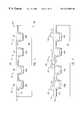
- FIGS. 1, 2 and 3are cross section illustrations of a packaging wafer (packaging substrate) at different stages of fabrication according to the present invention.
- FIGS. 8-11are cross section illustrations of a two-wafer structure at different stages of fabrication according to the present invention.
- FIG. 12is a cross section illustration of a wafer during fabrication according to the present invention.
- FIG. 13Ais a plan view of a wafer according to the present invention.
- FIG. 13Bis a cross section illustration of the wafer of FIG. 13 A.
- FIG. 17is a cross section illustration of a three-wafer structure during fabrication according to the present invention.
- FIG. 1shows a cross section of a wafer 110 at a beginning stage of fabrication.
- Wafer 110will provide a first level packaging substrate for another wafer 120 (FIG. 11 ).
- the “face” side 110 F of wafer 110will be bonded to wafer 120 , and the “back” side 110 B to a second level wiring substrate, for example, a printed circuit board 130 (FIG. 11 ).
- wafer 110is made of silicon. However, other semiconductor and non-semiconductor materials can be used instead.
- the beginning thickness of wafer 110(of silicon substrate 140 ) is 600-750 ⁇ m, or some other value, chosen to achieve suitable mechanical strength and heat dissipation during manufacturing The final thickness will be smaller.
- Back side contacts (conductive bumps) 150 B on the wafer back side 110 Bare formed from metal 150 .
- vias 160are etched in face side 110 F of silicon substrate 140 at the locations at which the back side contacts will be formed. Suitable etching processes include those used to form back side contacts for vertical integration as described in PCT publication WO 98/19337 “Integrated Circuits and Methods for Their Fabrication” (TruSi Technologies, LLC, May 7, 1999) incorporated herein by reference.
- the siliconis etched in atmospheric pressure plasma.
- the etcheris of type Tru-Etch 3000 (Trademark) available from Tru-Si Technologies, Inc., of Sunnyvale, Calif.
- each via 160is chosen based on the final thickness of wafer 110 and the dimensions of the corresponding back side contact 150 B, as described below.
- the via sidewallscan be vertical if the etch is perfectly anisotropic, or they can be sloped, and they can be either straight or rounded. Bowl-like vias with rounded corners (see FIG. 7) can be created by an atmospheric pressure plasma etch.
- a dielectric layer 170is deposited over the wafer's face side, as described in the aforementioned publication WO 98/19337.
- dielectric 170is BPSG deposited by chemical vapor deposition at atmospheric pressure.
- Other processese.g., thermal oxidation of silicon or plasma enhanced chemical vapor deposition
- other insulating materialse.g., undoped silicon dioxide, silicon nitride, or oxynitride
- S. Wolfe et al.“Silicon Processing for the VLSI Era”, Volume 1 (1986).
- metal 150is deposited as described in WO 98/19337.
- metal 150is aluminum, gold, nickel vanadium (NiV), titanium tungsten (TiW), or some other metal suitable for bonding to a second level packaging substrate.
- Metal 150can be deposited by sputtering or other known techniques.
- Layer 150can be a combination of different conductive layers, including possibly non-metal layers.
- the filler 180increases the wafer mechanical strength and provides a planar top surface.
- layers 150 and 230are patterned (FIG. 3) to provide interconnects between face side contacts 210 and back side contacts 150 B.
- the same mask(not shown) is used to pattern both layers. If both layers are made of the same material (e.g., aluminum), the same etch can be used for both.
- a dielectric passivation layer 410(FIG. 4) is formed on face side 110 F of wafer 110 .
- spin-on-glass, polymer (e.g., polyimide), epoxy, or some other suitable low viscosity materialis spun on or sprayed on the wafer so that the material is less thick over the bumps 210 than elsewhere. Then the material is dried or cured at a temperature of 120° C. to 200° C. The temperature depends on the material. After the material has been deposited, an etch-back is performed until the bumps 210 protrude from the top surface of passivation 410 by some amount suitable for bonding the wafer 110 to wafer 120 (5 to 50 ⁇ m in some embodiments).
- the etchcan be performed in vacuum plasma or atmospheric-pressure plasma.
- the etch chemistrydepends on the material of layer 410 , as known in the art. For example, if layer 410 is polymer, then oxygen plasma is appropriate. If layer 410 is spin-on glass, fluorine containing plasma can be used.
- circuitry(not shown) is manufactured in wafer 120 , including possibly transistors or other active devices in or adjacent to the wafer's face side 120 F.
- Contact pads 420are made on the wafer face side 120 F from a material suitable for bonding with metal 230 by whatever bonding process is used. Before or after bonding, wafer 120 can be thinned from the back side if needed.
- the waferscan be bonded with conductive or anisotropic adhesive.
- Soldercan also be used (solder bumps can be grown on contact pads 420 ). See U.S. Pat. No. 5,831,832 (Nov. 3, 1998, Gillette et al.), U.S. Pat. No. 5,786,271 (Jul. 28, 1998, Ohida et al.), and U.S. Pat. No. 5,918,113 (Jun. 29, 1999, Higashi et al.) describing some bonding methods and materials. Other materials and bonding methods are used in other embodiments.
- bumps 490are bonded directly to a PCB. Wafer 110 is omitted.
- layer 220 on wafer 110is omitted.
- Bumps 210 on wafer 110are made of solder, nickel vanadium, gold, or some other material suitable for bonding, using known techniques (e.g., solder evaporation or electroplating).
- bumps 210 on wafer 110are omitted. Bumps are formed on wafer 120 (e.g., by the process of FIG. 6 or using conventional solder, nickel vanadium, or gold technology), but not on wafer 110 .
- Wafer 120can be made of silicon or non-silicon material, not necessarily the same material as wafer 10 . However, if the same materials are used for the two wafers, their thermal expansion coefficients will advantageously be the same.
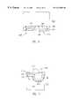
- FIG. 8shows the resulting structure for the face side contacts embodiment of FIGS. 4 and 5.
- the vias 160are exposed (they become through holes) and the metal 150 protrudes out of the wafer back side 110 B by at least a predetermined amount D 1 .
- D 1is 10 ⁇ m or greater.
- the siliconis removed by a blanket (non-masked) process, which can be a dry etch, erg., an atmospheric pressure plasma etch of the kind described in the aforementioned publication WO 98/19337. The etch can be preceded by mechanical grinding. Other processes can also be used.
- the circuitry on the face sides 110 F, 120 F of the two wafersis protected by the wafers and the adhesive 510 . Further, because the wafers have been bonded together, the structure is mechanically stronger, and heat dissipation is improved. Also, warpage of wafer 110 is lessened or eliminated (very thin wafers can be warped by stresses caused by the presence of metal or other materials in the wafers).
- the dielectric 170when the dielectric 170 becomes exposed on the back side during the etch, the dielectric is etched slower than the rest of the wafer.
- the dielectricis silicon dioxide, and the dielectric is etched 8 to 10 times slower, as described in WO 98/19337.
- the dielectricprotrudes down from the back side surface of silicon 140 around the contacts 150 B. The protruding dielectric improves electrical insulation of silicon 140 during subsequent attachment of the wafer to wiring substrate 130 (FIG. 11 ).
- layer 710is polyimide, glass, or some other flowable material (e.g., flowable thermosetting polymer) which can be deposited by a spin-on or spraying process and which is dielectric when cured. Low viscosity materials are particularly suitable but low viscosity is not necessary.
- the top surface of layer 710is substantially planar.
- the thickness of layer 710 over the metal contacts 150 Bis 0.5 to 5 ⁇ m. Other thicknesses can also be used.
- the top surface of layer 710is not planar, and layer 710 does not necessarily cover the contacts 150 B. At any rate, if layer 710 covers the contacts, the layer 710 is thinner over the contacts 150 B than between the contacts.
- Layer 710is etched by a blanket etch (FIG. 10) until the contacts 150 B protrude by a distance D 2 , which is 2 to 20 ⁇ m in some embodiments. If layer 710 is polyimide, the etch can be performed in atmospheric pressure oxygen plasma in an etcher of type Tru-Etch 3000.
- the two-wafer sandwichis diced if needed, to provide separate two-die structures. (In some embodiments, the wafers are not diced.)
- the two-wafer structure, or each two-die structureis attached to a wiring substrate such as PCB 130 (FIG. 11 ).
- contacts 150 Bare attached to the PCB using solder paste 910 deposited on PCB contacts 912 by a known process. Diffusion bonding, conductive or anisotropic adhesive, or other techniques, known or to be invented, can also be used.
- Underfill 920is introduced between the PCB and the wafer or die sandwich to increase mechanical strength.
- Plastic encapsulant(not shown) is deposited over the dies or wafers using known techniques.
- the final dimensions of protruding contacts 150 Bcan be chosen to accommodate the technology used for attaching the wafer or die sandwich to the PCB.
- the dimensionscan be controlled by controlling the size of vias 160 , the back side etch parameters for the etch of wafer 110 , and the thickness of layer 710 or any other insulator grown on the wafer back side
- the bottom surface of each contact 150 Bis a square having a side of 20 ⁇ m or greater.
- the contacts 150 Bmay have a rounded shape and look like a circle in the bottom view, of a radius 20 ⁇ m or greater
- the height of each contact, measured to the bottom surface of layer 710 (in the view of FIG. 11)is 10 to 20 ⁇ m. Other dimensions are also possible.
- Contacts 150 Bcan be evenly distributed on the back side surface 110 F of wafer 110 to provide an area matched package (as shown in FIG. 13 A). In some embodiments, the distance between the centers of the adjacent contacts is 75 to 1000 ⁇ m. Other distances can be used as needed to accommodate tolerances of the process of attaching the wafers to the PCB.
- the wafer 110can be manufactured using processes common in semiconductor fabrication, without using uncommon processes such as electroplating or solder evaporation.
- solder bumping on wafers 110 and 120is advantageous because solder bumping tolerances do not have to be accommodated.
- Contacts 210 on the wafer face side 110 Fcan be made with smaller lateral dimensions, and can be positioned closer together to match high precision semiconductor fabrication technology that can be used to manufacture the wafer 120 .
- Other disadvantages of solder bumpingare also eliminated, such as different bumps having different heights or bumps being lost due to solder collapse.
- the inventionis not limited to such embodiments. Some embodiments use solder bumping.
- wafer 110is made of a dielectric material, for example, a polymer. Suitable polymers include polyimide. Dielectric layers 170 , 710 can be omitted.
- Wafer 110can contain multiple layers of wiring as needed to connect the contacts 210 to back side contacts 150 B.
- FIG. 11illustrates certain structural features of the chip or wafer 110 .
- the chip or waferincludes a semiconductor or insulating substrate 140 .
- the substratehas one or more through holes in it.
- a contact 150 Bis provided in each of the holes.
- Each contact 150 Bincludes at least one conductive layer 150 protruding down from the chip or wafer 110 through at least one hole.
- the conductive layer 150also goes inside the substrate 140 and extends laterally away form the hole.
- layer 1020represents one or more layers formed during the wafer 110 fabrication.
- Bumps 210are formed above layer 1020 .
- Metal 230contacts metal 150 through a via 1024 in layer 1020 . Alternatively, the contact can be made through intermediate layers (not shown) using multiple vias. After the bumps 210 are formed, fabrication proceeds as described above in connection with FIGS. 4-11.
- the circuitry in wafer 110includes ESD (electrostatic discharge) or overvoltage protection circuits, or some other circuits encountered in different types of devices.
- ESDelectrostatic discharge
- overvoltage protection circuitsor some other circuits encountered in different types of devices.
- the same wafer 110 designcan be combined with different kinds of wafers 120 .
- Other examples of such circuits in wafer 110include voltage regulators and DC converters.
- wafer 110includes a voltage converter that converts a 3.3V power supply voltage available on the PCB to a 1.2V supply voltage.
- wafer 110includes a converter that receives a 5V power supply voltage from the PCB and generates both 3.3V and 1.2V supply voltages for wafer 120 . Voltage converters and regulators sometimes occupy large area and consume much power (generate much heat). Removing such circuits from wafer 120 to wafer or die 110 is therefore advantageous.
- wafer 120is omitted. All the circuitry is in wafer 110 . No contacts are formed on the face side of wafer 110 . Thus, the layers 220 , 230 are omitted.
- the wafer 110or individual chips obtained from the wafer, are directly attached to a PCB or another wiring substrate as first level packaging. The attachment is made using back side contacts 150 B.
- Back side contacts 150 Bcan be used as alignment marks when wafer 110 or the wafer sandwich 110 , 120 is diced. Additional alignment marks can be created along the scribe lines as shown in FIGS. 13A and 13B.
- FIG. 13Ashows the wafer 110 back side before dicing. In this example, the wafer includes four chips 110 C. Back side contacts 150 B are shown on only one of the chips for simplicity.
- Lines 1110are scribe lines along which the wafer sandwich will be diced.
- vias 1120(FIG. 13B) are etched in the face side 110 F at the same time as vias 160 to form additional alignment marks. Vias 1120 can be made narrow to occupy less wafer area.
- the filler in vias 1120is different from the filler in vias 160 .
- the filler in vias 1120can be soft material to reduce the stress on the silicon substrate 140 when the wafer is diced. Further, before dicing, the filler in vias 1120 can be etched away.
- dicingis accomplished by simply breaking the wafers along the scribe lines 1110 .
- Wafer 120has vias (not shown) similar to vias 1120 , along the scribe lines.
- the vias in wafer 120are filled with soft material.
- back side 120 B (FIG. 5) of wafer 120is etched to expose the vias. This etch can be done after the wafers 110 and 120 are bonded together, so that the wafer 120 face side is protected.
- the wafer sandwichis sawed part of the way, and then broken.
- dielectric 170is etched off the metal 150 to expose the back side contacts 150 B (FIG. 16 ).
- dielectric 170is silicon dioxide
- metal 150is aluminum
- the etchis performed in a fluorine-containing plasma. Fluorine does not react with aluminum or with polyimide 710 .
- back side 120 B of wafer 120is bonded to a third wafer 1510 before the wafer 110 back side contacts 150 B are exposed.
- Wafer 120contains back side contacts 150 B similar to contacts 150 B in wafer 110 .
- Wafer 120 of FIG. 17also contains a substrate 140 , an insulator 170 , passivation 710 , and intermediate layer or layers 1020 , such as described above for wafer 110 (FIG. 12 ).
- Other structures for wafer 120are possible, such as used in vertical integrated circuits. See, for example, the aforementioned PCT publication WO 98/19337 (TruSi Technologies).
- the contacts 150 B of wafer 120are exposed after the wafers 110 and 120 have been bonded.
- the contactscan be exposed using the processes described above for wafer 110 (see FIGS. 8-16 and accompanying text).
- Wafer 120can be bonded to wafer 1510 using the bonding processes described above for bonding the wafer 120 to wafer 110 (FIGS. 4 and 5 ), or other processes used in vertical integration.
- face side contacts 420 and passivation 430 in wafer 1510are similar to those in wafer 120 .
- Other embodimentsuse dissimilar contact structures in the two wafers.
- wafer 1510also has back side contacts (not shown). After the wafers 120 and 1510 have been bonded, these contacts are exposed, and additional wafers are bonded to the back side 1510 B of wafer 1510 .
- Passivation 430 on the face side of wafer 120is etched to expose the wafer's contacts 420 .
- Wafer 120is bonded to wafer 110 .
- a stack of wafers 120 . 1 through 120 . 6is attached to first level packaging wafer 110 , which is attached to PCB 130 .
- the suffix F in numerals such as 120 . 2 Findicates the face side of the corresponding wafer, and the suffix B indicates the back side.
- the face sidemay have active circuitry (e.g., transistors).
- Each of wafers 120 . 1 through 120 . 5has back side contacts attached to another wafer.
- the structure of FIG. 18is manufactured as follows. First, the wafers 120 . 1 and 120 . 2 are bonded together, face side 120 . 1 F to face side 120 . 2 F, before any back side contacts on any wafers are exposed. Then one of the wafers 120 . 1 , 120 . 2 has its back side contacts exposed and bonded to the face side of another wafer. For example, back side 120 . 1 B of wafer 120 . 1 is bonded to face side 120 . 4 F of wafer 120 . 4 . Then one of the two end wafers ( 120 . 2 or 120 . 4 ) has its back side contacts exposed and bonded to the face side of another wafer, and so on, until the whole stack of wafers 120 . 1 - 120 . 6 and 110 has been assembled. Then the wafer 110 back side contacts are exposed, dicing is performed if needed, and the wafer stack or each chip stack is bonded to the PCB.
- Encapsulant 1610(e.g., suitable resin) is deposited to encapsulate the wafer stack or each chip stack using known techniques.
- the wafers 110 , 120 . 1 - 120 . 6 of FIG. 18have similar face side contact structures, and the wafers 110 , 120 . 1 - 120 . 5 have similar back side contact structures, except possibly that the back side contacts in wafer 110 are larger, and are spaced farther from each other, to accommodate the PCB fabrication and mounting tolerances.
- the size and shape of the back side contacts on wafers 120 . 1 - 120 . 5are as described above for FIG. 13A (20 ⁇ m radius or 20 ⁇ m square side). The distance between the centers of the adjacent contacts is 150 ⁇ m.
Landscapes
- Engineering & Computer Science (AREA)
- Microelectronics & Electronic Packaging (AREA)
- Power Engineering (AREA)
- Computer Hardware Design (AREA)
- Physics & Mathematics (AREA)
- Condensed Matter Physics & Semiconductors (AREA)
- General Physics & Mathematics (AREA)
- Manufacturing & Machinery (AREA)
- Internal Circuitry In Semiconductor Integrated Circuit Devices (AREA)
Abstract
Description
Claims (29)
Priority Applications (5)
| Application Number | Priority Date | Filing Date | Title |
|---|---|---|---|
| US09/456,225US6322903B1 (en) | 1999-12-06 | 1999-12-06 | Package of integrated circuits and vertical integration |
| US09/716,092US6693361B1 (en) | 1999-12-06 | 2000-11-16 | Packaging of integrated circuits and vertical integration |
| EP00982464.0AEP1247294B1 (en) | 1999-12-06 | 2000-12-06 | Packaging of integrated circuits and vertical integration |
| AU19493/01AAU1949301A (en) | 1999-12-06 | 2000-12-06 | Packaging of integrated circuits and vertical integration |
| PCT/US2000/033073WO2001041207A1 (en) | 1999-12-06 | 2000-12-06 | Packaging of integrated circuits and vertical integration |
Applications Claiming Priority (1)
| Application Number | Priority Date | Filing Date | Title |
|---|---|---|---|
| US09/456,225US6322903B1 (en) | 1999-12-06 | 1999-12-06 | Package of integrated circuits and vertical integration |
Related Child Applications (1)
| Application Number | Title | Priority Date | Filing Date |
|---|---|---|---|
| US09/716,092DivisionUS6693361B1 (en) | 1999-12-06 | 2000-11-16 | Packaging of integrated circuits and vertical integration |
Publications (1)
| Publication Number | Publication Date |
|---|---|
| US6322903B1true US6322903B1 (en) | 2001-11-27 |
Family
ID=23811960
Family Applications (2)
| Application Number | Title | Priority Date | Filing Date |
|---|---|---|---|
| US09/456,225Expired - LifetimeUS6322903B1 (en) | 1999-12-06 | 1999-12-06 | Package of integrated circuits and vertical integration |
| US09/716,092Expired - LifetimeUS6693361B1 (en) | 1999-12-06 | 2000-11-16 | Packaging of integrated circuits and vertical integration |
Family Applications After (1)
| Application Number | Title | Priority Date | Filing Date |
|---|---|---|---|
| US09/716,092Expired - LifetimeUS6693361B1 (en) | 1999-12-06 | 2000-11-16 | Packaging of integrated circuits and vertical integration |
Country Status (4)
| Country | Link |
|---|---|
| US (2) | US6322903B1 (en) |
| EP (1) | EP1247294B1 (en) |
| AU (1) | AU1949301A (en) |
| WO (1) | WO2001041207A1 (en) |
Cited By (504)
| Publication number | Priority date | Publication date | Assignee | Title |
|---|---|---|---|---|
| US20020116668A1 (en)* | 2001-02-20 | 2002-08-22 | Matrix Semiconductor, Inc. | Memory card with enhanced testability and methods of making and using the same |
| US6483736B2 (en)* | 1998-11-16 | 2002-11-19 | Matrix Semiconductor, Inc. | Vertically stacked field programmable nonvolatile memory and method of fabrication |
| US6498381B2 (en) | 2001-02-22 | 2002-12-24 | Tru-Si Technologies, Inc. | Semiconductor structures having multiple conductive layers in an opening, and methods for fabricating same |
| US6525415B2 (en)* | 1999-12-28 | 2003-02-25 | Fuji Xerox Co., Ltd. | Three-dimensional semiconductor integrated circuit apparatus and manufacturing method therefor |
| US6525953B1 (en) | 2001-08-13 | 2003-02-25 | Matrix Semiconductor, Inc. | Vertically-stacked, field-programmable, nonvolatile memory and method of fabrication |
| US20030059976A1 (en)* | 2001-09-24 | 2003-03-27 | Nathan Richard J. | Integrated package and methods for making same |
| US20030068840A1 (en)* | 2000-04-28 | 2003-04-10 | Grigg Ford B. | Interposers including upwardly protruding dams, semiconductor device assemblies including the interposers, and methods |
| US6593624B2 (en) | 2001-09-25 | 2003-07-15 | Matrix Semiconductor, Inc. | Thin film transistors with vertically offset drain regions |
| US20030148552A1 (en)* | 2001-09-13 | 2003-08-07 | Halahan Patrick B. | Semiconductor structures with cavities, and methods of fabrication |
| US20030151132A1 (en)* | 2002-02-14 | 2003-08-14 | Crippen Warren Stuart | Microelectronic die providing improved heat dissipation, and method of packaging same |
| US20030153119A1 (en)* | 2002-02-14 | 2003-08-14 | Nathan Richard J. | Integrated circuit package and method for fabrication |
| US6620649B2 (en)* | 2001-04-24 | 2003-09-16 | Oki Electric Industry Co., Ltd. | Method for selectively providing adhesive on a semiconductor device |
| US6624485B2 (en) | 2001-11-05 | 2003-09-23 | Matrix Semiconductor, Inc. | Three-dimensional, mask-programmed read only memory |
| WO2003079430A1 (en) | 2002-03-19 | 2003-09-25 | Seiko Epson Corporation | Semiconductor device and its manufacturing method, circuit board and electronic apparatus |
| US20030183920A1 (en)* | 2002-03-28 | 2003-10-02 | Goodrich Joel Lee | Hermetic electric component package |
| US6635548B2 (en)* | 2000-02-07 | 2003-10-21 | International Business Machines Corporation | Capacitor and method for forming same |
| US20030199121A1 (en)* | 2000-07-27 | 2003-10-23 | Caletka David Vincent | Wafer scale thin film package |
| US20040020040A1 (en)* | 2002-08-02 | 2004-02-05 | Matrics, Inc. | Method and system for forming a die frame for transferring dies therewith |
| US20040020036A1 (en)* | 2002-08-02 | 2004-02-05 | Matrics, Inc. | Method and apparatus for high volume assembly of radio frequency identification tags |
| US20040021139A1 (en)* | 2002-07-31 | 2004-02-05 | Jackson Timothy L. | Semiconductor dice having backside redistribution layer accessed using through-silicon vias, methods of fabrication and assemblies |
| US20040055893A1 (en)* | 2002-09-23 | 2004-03-25 | Applied Materials, Inc. | Wafer backside electrical contact for electrochemical deposition and electrochemical mechanical polishing |
| US20040063322A1 (en)* | 2000-11-02 | 2004-04-01 | Eui-Hyeok Yang | Wafer-level transfer of membranes with gas-phase etching and wet etching methods |
| US6717254B2 (en)* | 2001-02-22 | 2004-04-06 | Tru-Si Technologies, Inc. | Devices having substrates with opening passing through the substrates and conductors in the openings, and methods of manufacture |
| WO2003065450A3 (en)* | 2002-01-28 | 2004-04-08 | Tru Si Technologies Inc | Integrated circuits with backside contacts and methods for their fabrication |
| US6730540B2 (en) | 2002-04-18 | 2004-05-04 | Tru-Si Technologies, Inc. | Clock distribution networks and conductive lines in semiconductor integrated circuits |
| US6731011B2 (en) | 2002-02-19 | 2004-05-04 | Matrix Semiconductor, Inc. | Memory module having interconnected and stacked integrated circuits |
| US6737675B2 (en) | 2002-06-27 | 2004-05-18 | Matrix Semiconductor, Inc. | High density 3D rail stack arrays |
| US20040115919A1 (en)* | 2001-05-14 | 2004-06-17 | Yuji Takaoka | Semiconductor device and its manufacturing method |
| US20040142574A1 (en)* | 2002-03-19 | 2004-07-22 | Seiko Epson Corporation | Semiconductor device and method of manufacturing the same, circuit board, and electronic instrument |
| US20040157461A1 (en)* | 2003-02-10 | 2004-08-12 | Seh America, Inc. | Method for fabricating a wafer including dry etching the edge of the wafer |
| US6777312B2 (en)* | 2000-11-02 | 2004-08-17 | California Institute Of Technology | Wafer-level transfer of membranes in semiconductor processing |
| US20040161926A1 (en)* | 2003-01-24 | 2004-08-19 | Seiko Epson Corporation | Method for manufacturing semiconductor device, and method for manufacturing semiconductor module |
| US6794272B2 (en) | 2001-10-26 | 2004-09-21 | Ifire Technologies, Inc. | Wafer thinning using magnetic mirror plasma |
| US20040203224A1 (en)* | 2003-04-09 | 2004-10-14 | Halahan Patrick A. | Electroplating and electroless plating of conductive materials into openings, and structures obtained thereby |
| US6818474B2 (en) | 2001-12-29 | 2004-11-16 | Hynix Semiconductor Inc. | Method for manufacturing stacked chip package |
| US20040250949A1 (en)* | 2003-06-12 | 2004-12-16 | Matrics, Inc. | Method and apparatus for expanding a semiconductor wafer |
| US6841813B2 (en) | 2001-08-13 | 2005-01-11 | Matrix Semiconductor, Inc. | TFT mask ROM and method for making same |
| US6843421B2 (en) | 2001-08-13 | 2005-01-18 | Matrix Semiconductor, Inc. | Molded memory module and method of making the module absent a substrate support |
| US6853049B2 (en) | 2002-03-13 | 2005-02-08 | Matrix Semiconductor, Inc. | Silicide-silicon oxide-semiconductor antifuse device and method of making |
| US20050048698A1 (en)* | 2003-07-31 | 2005-03-03 | Seiko Epson Corporation | Semiconductor device, method for manufacturing the same, circuit board, and electronic apparatus |
| US6881994B2 (en) | 2000-08-14 | 2005-04-19 | Matrix Semiconductor, Inc. | Monolithic three dimensional array of charge storage devices containing a planarized surface |
| US6888750B2 (en) | 2000-04-28 | 2005-05-03 | Matrix Semiconductor, Inc. | Nonvolatile memory on SOI and compound semiconductor substrates and method of fabrication |
| US20050101056A1 (en)* | 2002-02-06 | 2005-05-12 | Song Young H. | Semiconductor chip, chip stack package and manufacturing method |
| US6897514B2 (en) | 2001-03-28 | 2005-05-24 | Matrix Semiconductor, Inc. | Two mask floating gate EEPROM and method of making |
| US20050133930A1 (en)* | 2003-12-17 | 2005-06-23 | Sergey Savastisuk | Packaging substrates for integrated circuits and soldering methods |
| US20050136634A1 (en)* | 2003-12-17 | 2005-06-23 | Sergey Savastiouk | Integrated circuits and packaging substrates with cavities, and attachment methods including insertion of protruding contact pads into cavities |
| US20050151699A1 (en)* | 2004-01-12 | 2005-07-14 | Symbol Technologies, Inc. | Method and system for manufacturing radio frequency identification tag antennas |
| US20050155213A1 (en)* | 2004-01-12 | 2005-07-21 | Symbol Technologies, Inc. | Radio frequency identification tag inlay sortation and assembly |
| EP1470583A4 (en)* | 2001-12-19 | 2005-08-03 | Ibm | Chip and wafer integration process using vertical connections |
| US20050167829A1 (en)* | 2004-01-29 | 2005-08-04 | Brunner Dennis M. | Partially etched dielectric film with conductive features |
| US20050224590A1 (en)* | 2004-04-13 | 2005-10-13 | John Melngailis | Method and system for fabricating integrated circuit chips with unique identification numbers |
| US20050224921A1 (en)* | 2001-05-01 | 2005-10-13 | Subhash Gupta | Method for bonding wafers to produce stacked integrated circuits |
| US20050266613A1 (en)* | 2003-03-31 | 2005-12-01 | Intel Corporation | Integrated circuit packages with reduced stress on die and associated methods |
| US20060012387A1 (en)* | 2004-06-29 | 2006-01-19 | Symbol Technologies, Inc. | Systems and methods for testing radio frequency identification tags |
| US20060040467A1 (en)* | 2004-08-20 | 2006-02-23 | Dolechek Kert L | Process and apparatus for thinning a semiconductor workpiece |
| US20060040111A1 (en)* | 2004-08-20 | 2006-02-23 | Dolechek Kert L | Process chamber and system for thinning a semiconductor workpiece |
| US20060043569A1 (en)* | 2004-08-27 | 2006-03-02 | Benson Peter A | Low temperature methods of forming back side redistribution layers in association with through wafer interconnects, semiconductor devices including same, and assemblies |
| US20060046499A1 (en)* | 2004-08-20 | 2006-03-02 | Dolechek Kert L | Apparatus for use in thinning a semiconductor workpiece |
| US20060118515A1 (en)* | 2004-08-20 | 2006-06-08 | Semitool, Inc. | Process For Thinning A Semiconductor Workpiece |
| US7098518B1 (en) | 2003-08-27 | 2006-08-29 | National Semiconductor Corporation | Die-level opto-electronic device and method of making same |
| US20060199353A1 (en)* | 2002-07-12 | 2006-09-07 | The Government Of The Usa, As Represented By The Secretary Of The Navy Naval Research Laboratory | Wafer bonding of thinned electronic materials and circuits to high performance substrate |
| US20060223225A1 (en)* | 2005-03-29 | 2006-10-05 | Symbol Technologies, Inc. | Method, system, and apparatus for transfer of integrated circuit dies using an attractive force |
| US20060246621A1 (en)* | 2002-02-14 | 2006-11-02 | Intel Corporation | Microelectronic die including thermally conductive structure in a substrate thereof and method of forming same |
| US7187293B2 (en) | 2004-08-17 | 2007-03-06 | Symbol Technologies, Inc. | Singulation of radio frequency identification (RFID) tags for testing and/or programming |
| EP1763079A1 (en)* | 2005-09-07 | 2007-03-14 | Irvine Sensors Corporation | Stackable semiconductor chip layer comprising prefabricated trench interconnect vias |
| US20070131016A1 (en)* | 2005-12-13 | 2007-06-14 | Symbol Technologies, Inc. | Transferring die(s) from an intermediate surface to a substrate |
| US20070134855A1 (en)* | 2005-12-09 | 2007-06-14 | Macronix International Co., Ltd. | A stacked non-volatile memory device and methods for fabricating the same |
| US20070139057A1 (en)* | 2005-12-15 | 2007-06-21 | Symbol Technologies, Inc. | System and method for radio frequency identification tag direct connection test |
| US20070158024A1 (en)* | 2006-01-11 | 2007-07-12 | Symbol Technologies, Inc. | Methods and systems for removing multiple die(s) from a surface |
| US20070210437A1 (en)* | 2006-03-07 | 2007-09-13 | Sanyo Electric Co., Ltd. | Semiconductor device and manufacturing method thereof |
| US20070244657A1 (en)* | 2006-04-11 | 2007-10-18 | Drago Randall A | Methods and systems for testing radio frequency identification (RFID) tags having multiple antennas |
| US20070257367A1 (en)* | 2006-05-05 | 2007-11-08 | Tru-Si Technologies, Inc. | Dielectric trenches, nickel/tantalum oxide structures,and chemical mechanical polishing techniques |
| DE10346581B4 (en)* | 2003-01-14 | 2007-12-27 | Renesas Technology Corp. | Method for producing a semiconductor device |
| US7354649B2 (en) | 2004-08-20 | 2008-04-08 | Semitool, Inc. | Semiconductor workpiece |
| US20080116462A1 (en)* | 2006-09-28 | 2008-05-22 | Renesas Technology Corp. | Semiconductor device |
| US20080135967A1 (en)* | 2006-11-20 | 2008-06-12 | Sanyo Electric Co., Ltd. | Semiconductor device and method of manufacturing the same |
| US20080173993A1 (en)* | 2007-01-18 | 2008-07-24 | International Business Machines Corporation | Chip carrier substrate capacitor and method for fabrication thereof |
| US7473589B2 (en)* | 2005-12-09 | 2009-01-06 | Macronix International Co., Ltd. | Stacked thin film transistor, non-volatile memory devices and methods for fabricating the same |
| US20090039414A1 (en)* | 2007-08-09 | 2009-02-12 | Macronix International Co., Ltd. | Charge trapping memory cell with high speed erase |
| US20090102021A1 (en)* | 2007-10-17 | 2009-04-23 | Chih-Hua Chen | Through-Silicon Vias and Methods for Forming the Same |
| US20090134500A1 (en)* | 2007-11-26 | 2009-05-28 | Chen-Cheng Kuo | Structures for Preventing Cross-talk Between Through-Silicon Vias and Integrated Circuits |
| US20090186430A1 (en)* | 2007-05-24 | 2009-07-23 | Chih-Hua Chen | Test Patterns for Detecting Misalignment of Through-Wafer Vias |
| US20090193584A1 (en)* | 2008-02-05 | 2009-08-06 | Standard Textile Co., Inc. | Woven contoured bed sheet with elastomeric yarns |
| US20090283871A1 (en)* | 2008-05-14 | 2009-11-19 | Hung-Pin Chang | System, Structure, and Method of Manufacturing a Semiconductor Substrate Stack |
| US20090321888A1 (en)* | 2007-12-06 | 2009-12-31 | Taiwan Semiconductor Manufacturing Company, Ltd. | Alignment for backside illumination sensor |
| US20100038674A1 (en)* | 2008-08-18 | 2010-02-18 | Ding-Yuan Chen | Light-Emitting Diode With Current-Spreading Region |
| US20100038800A1 (en)* | 2008-08-18 | 2010-02-18 | Samsung Electronics Co., Ltd. | Through-silicon via structures including conductive protective layers and methods of forming the same |
| US20100044860A1 (en)* | 2008-08-21 | 2010-02-25 | Tessera Interconnect Materials, Inc. | Microelectronic substrate or element having conductive pads and metal posts joined thereto using bond layer |
| US20100062693A1 (en)* | 2008-09-05 | 2010-03-11 | Taiwan Semiconductor Manufacturing Co., Ltd. | Two step method and apparatus for polishing metal and other films in semiconductor manufacturing |
| US20100084747A1 (en)* | 2008-10-03 | 2010-04-08 | Chih-Hua Chen | Zigzag Pattern for TSV Copper Adhesion |
| US20100090304A1 (en)* | 2008-09-08 | 2010-04-15 | Taiwan Semiconductor Manufacturing Company, Ltd. | Bonding process for cmos image sensor |
| US20100117201A1 (en)* | 2008-11-13 | 2010-05-13 | Kai-Ming Ching | Cooling Channels in 3DIC Stacks |
| US20100144094A1 (en)* | 2008-12-05 | 2010-06-10 | Ming-Fa Chen | Method of Forming Stacked Dies |
| US20100140805A1 (en)* | 2008-12-10 | 2010-06-10 | Hung-Pin Chang | Bump Structure for Stacked Dies |
| US20100140772A1 (en)* | 2008-12-08 | 2010-06-10 | Stats Chippac, Ltd. | Semiconductor Device and Method of Forming Vertical Interconnect Structure in Substrate for IPD and Baseband Circuit Separated by High-Resistivity Molding Compound |
| US20100148353A1 (en)* | 2008-12-11 | 2010-06-17 | Stats Chippac, Ltd. | Double-Sided Semiconductor Device and Method of Forming Top-Side and Bottom-Side Interconnect Structures |
| US20100164086A1 (en)* | 2006-08-11 | 2010-07-01 | Sanyo Electric Co., Ltd. | Semiconductor device and manufacturing method thereof |
| US20100164109A1 (en)* | 2008-12-29 | 2010-07-01 | Wen-Chih Chiou | Backside Metal Treatment of Semiconductor Chips |
| US20100171197A1 (en)* | 2009-01-05 | 2010-07-08 | Hung-Pin Chang | Isolation Structure for Stacked Dies |
| US20100171203A1 (en)* | 2009-01-07 | 2010-07-08 | Taiwan Semiconductor Manufacturing Company | Robust TSV structure |
| US20100176494A1 (en)* | 2009-01-13 | 2010-07-15 | Ming-Fa Chen | Through-Silicon Via With Low-K Dielectric Liner |
| US20100187670A1 (en)* | 2009-01-26 | 2010-07-29 | Chuan-Yi Lin | On-Chip Heat Spreader |
| US20100193954A1 (en)* | 2009-02-04 | 2010-08-05 | Max Liu | Barrier Structures and Methods for Through Substrate Vias |
| US20100194014A1 (en)* | 2009-02-02 | 2010-08-05 | Jao Sheng Huang | Semiconductor Wafer Carrier |
| US20100220226A1 (en)* | 2009-02-24 | 2010-09-02 | Taiwan Semiconductor Manufacturing Company, Ltd. | Front side implanted guard ring structure for backside illuminated image sensor |
| US20100224966A1 (en)* | 2009-03-03 | 2010-09-09 | Taiwan Semiconductor Manufacturing Company, Ltd. | Stress Barrier Structures for Semiconductor Chips |
| US20100225002A1 (en)* | 2009-03-06 | 2010-09-09 | Taiwan Semiconductor Manufacturing Company, Ltd. | Three-Dimensional System-in-Package Architecture |
| US20100237502A1 (en)* | 2009-03-23 | 2010-09-23 | Taiwan Semiconductor Manufacturing Company, Ltd. | Barrier for Through-Silicon Via |
| US20100244247A1 (en)* | 2009-03-27 | 2010-09-30 | Taiwan Semiconductor Manufacturing Company, Ltd. | Via structure and via etching process of forming the same |
| US20100244284A1 (en)* | 2009-03-27 | 2010-09-30 | Taiwan Semiconductor Manufacturing Company, Ltd. | Method for ultra thin wafer handling and processing |
| US20100252934A1 (en)* | 2009-04-07 | 2010-10-07 | Taiwan Semiconductor Manufacturing Company, Ltd. | Three-Dimensional Semiconductor Architecture |
| US7811890B2 (en) | 2006-10-11 | 2010-10-12 | Macronix International Co., Ltd. | Vertical channel transistor structure and manufacturing method thereof |
| US20100267217A1 (en)* | 2009-04-20 | 2010-10-21 | Taiwan Semiconductor Manufacturing Company, Ltd. | Backside Process for a Substrate |
| US20100276787A1 (en)* | 2009-04-30 | 2010-11-04 | Taiwan Semiconductor Manufacturing Company, Ltd. | Wafer Backside Structures Having Copper Pillars |
| US20100276786A1 (en)* | 2009-04-29 | 2010-11-04 | International Business Machines Corporation | Through Substrate Vias |
| US20100291735A1 (en)* | 1997-11-11 | 2010-11-18 | Volkan Ozguz | Stackable semiconductor chip layer comprising prefabricated trench interconnect vias |
| US20100314758A1 (en)* | 2009-06-12 | 2010-12-16 | Taiwan Semiconductor Manufacturing Company, Ltd. | Through-silicon via structure and a process for forming the same |
| US20100330798A1 (en)* | 2009-06-26 | 2010-12-30 | Taiwan Semiconductor Manufacturing Company, Ltd. | Formation of TSV Backside Interconnects by Modifying Carrier Wafers |
| US20100330788A1 (en)* | 2009-06-30 | 2010-12-30 | Taiwan Semiconductor Manufacturing Company, Ltd. | Thin wafer handling structure and method |
| US20110006428A1 (en)* | 2009-07-08 | 2011-01-13 | Ching-Yu Lo | Liner Formation in 3DIC Structures |
| US20110027944A1 (en)* | 2009-07-30 | 2011-02-03 | Taiwan Semiconductor Maufacturing Company, Ltd. | Method of forming electrical connections |
| US20110035937A1 (en)* | 2009-08-14 | 2011-02-17 | Taiwan Semiconductor Manufacturing Company, Ltd. | Semiconductor Wafer Carrier and Method of Manufacturing |
| US20110049706A1 (en)* | 2009-09-03 | 2011-03-03 | Taiwan Semiconductor Manufacturing Company, Ltd. | Front Side Copper Post Joint Structure for Temporary Bond in TSV Application |
| US7907450B2 (en) | 2006-05-08 | 2011-03-15 | Macronix International Co., Ltd. | Methods and apparatus for implementing bit-by-bit erase of a flash memory device |
| US20110065238A1 (en)* | 2009-09-14 | 2011-03-17 | Taiwan Semiconductor Manufacturing Company, Ltd. | Protection layer for adhesive material at wafer edge |
| US20110078127A1 (en)* | 2009-09-27 | 2011-03-31 | Alibaba Group Holding Limited | Searching for information based on generic attributes of the query |
| US20110081749A1 (en)* | 2009-10-01 | 2011-04-07 | Taiwan Semiconductor Manufacturing Company, Ltd. | Surface modification for handling wafer thinning process |
| US20110084365A1 (en)* | 2009-10-09 | 2011-04-14 | Taiwan Semiconductor Manufacturing Company, Ltd. | Through Silicon Via (TSV) Wire Bond Architecture |
| US20110101527A1 (en)* | 2009-11-05 | 2011-05-05 | Taiwan Semiconductor Manufacturing Company, Ltd. | Mechanisms for forming copper pillar bumps |
| US20110108986A1 (en)* | 2009-11-09 | 2011-05-12 | Taiwan Semiconductor Manufacturing Company, Ltd. | Through-silicon via structure and a process for forming the same |
| US20110108940A1 (en)* | 2009-11-06 | 2011-05-12 | Taiwan Semiconductor Manufacturing Company, Ltd. | Method of fabricating backside-illuminated image sensor |
| US20110133335A1 (en)* | 2008-12-31 | 2011-06-09 | Taiwan Semiconductor Manufacturing Company, Ltd. | Through-Silicon Via With Air Gap |
| US20110169168A1 (en)* | 2009-02-24 | 2011-07-14 | Taiwan Semiconductor Manufacturing Company, Ltd. | Through-silicon via formed with a post passivation interconnect structure |
| US20110177655A1 (en)* | 2007-06-27 | 2011-07-21 | Taiwan Semiconductor Manufacturing Company, Ltd. | Formation of Through Via before Contact Processing |
| US20110193219A1 (en)* | 2010-02-09 | 2011-08-11 | Taiwan Seimconductor Manufacturing Company, Ltd. | Semiconductor device and semiconductor assembly with lead-free solder |
| US20110193221A1 (en)* | 2010-02-05 | 2011-08-11 | Taiwan Semiconductor Manufacturing Company, Ltd. | 3DIC Architecture with Interposer for Bonding Dies |
| US20110198638A1 (en)* | 2010-02-16 | 2011-08-18 | Taiwan Semiconductor Manufacturing Company, Ltd. | Light-emitting diode (led) package systems |
| US20110198721A1 (en)* | 2010-02-12 | 2011-08-18 | Taiwan Semiconductor Manufacturing Company, Ltd. | Method for thinning a wafer |
| US20110198747A1 (en)* | 2010-02-16 | 2011-08-18 | Taiwan Semicondcutor Manufactoring Company, Ltd. | Conductive pillar structure for semiconductor substrate and method of manufacture |
| US20110217841A1 (en)* | 2009-10-22 | 2011-09-08 | Taiwan Semiconductor Manufacturing Company, Ltd. | Method of forming through silicon via with dummy structure |
| US20110217812A1 (en)* | 2008-02-22 | 2011-09-08 | Harry Hedler | Integrated circuit device and method for fabricating same with an interposer substrate |
| WO2012015550A2 (en) | 2010-07-30 | 2012-02-02 | Monolithic 3D, Inc. | Semiconductor device and structure |
| US20120074585A1 (en)* | 2010-09-24 | 2012-03-29 | Stats Chippac, Ltd. | Semiconductor Device and Method of Forming TSV Interposer With Semiconductor Die and Build-Up Interconnect Structure on Opposing Surfaces of the Interposer |
| US8163581B1 (en) | 2010-10-13 | 2012-04-24 | Monolith IC 3D | Semiconductor and optoelectronic devices |
| US8168529B2 (en) | 2009-01-26 | 2012-05-01 | Taiwan Semiconductor Manufacturing Company, Ltd. | Forming seal ring in an integrated circuit die |
| US8174124B2 (en) | 2010-04-08 | 2012-05-08 | Taiwan Semiconductor Manufacturing Co., Ltd. | Dummy pattern in wafer backside routing |
| US8203148B2 (en) | 2010-10-11 | 2012-06-19 | Monolithic 3D Inc. | Semiconductor device and structure |
| US8222139B2 (en) | 2010-03-30 | 2012-07-17 | Taiwan Semiconductor Manufacturing Company, Ltd. | Chemical mechanical polishing (CMP) processing of through-silicon via (TSV) and contact plug simultaneously |
| US8237228B2 (en) | 2009-10-12 | 2012-08-07 | Monolithic 3D Inc. | System comprising a semiconductor device and structure |
| US8236584B1 (en) | 2011-02-11 | 2012-08-07 | Tsmc Solid State Lighting Ltd. | Method of forming a light emitting diode emitter substrate with highly reflective metal bonding |
| US8247906B2 (en) | 2009-07-06 | 2012-08-21 | Taiwan Semiconductor Manufacturing Company, Ltd. | Supplying power to integrated circuits using a grid matrix formed of through-silicon vias |
| US8258810B2 (en) | 2010-09-30 | 2012-09-04 | Monolithic 3D Inc. | 3D semiconductor device |
| US8273610B2 (en) | 2010-11-18 | 2012-09-25 | Monolithic 3D Inc. | Method of constructing a semiconductor device and structure |
| US8283215B2 (en) | 2010-10-13 | 2012-10-09 | Monolithic 3D Inc. | Semiconductor and optoelectronic devices |
| US8294159B2 (en) | 2009-10-12 | 2012-10-23 | Monolithic 3D Inc. | Method for fabrication of a semiconductor device and structure |
| US8298875B1 (en) | 2011-03-06 | 2012-10-30 | Monolithic 3D Inc. | Method for fabrication of a semiconductor device and structure |
| US8319336B2 (en) | 2010-07-08 | 2012-11-27 | Taiwan Semiconductor Manufacturing Company, Ltd. | Reduction of etch microloading for through silicon vias |
| US8324738B2 (en) | 2009-09-01 | 2012-12-04 | Taiwan Semiconductor Manufacturing Company, Ltd. | Self-aligned protection layer for copper post structure |
| US8338939B2 (en) | 2010-07-12 | 2012-12-25 | Taiwan Semiconductor Manufacturing Company, Ltd. | TSV formation processes using TSV-last approach |
| US8362800B2 (en) | 2010-10-13 | 2013-01-29 | Monolithic 3D Inc. | 3D semiconductor device including field repairable logics |
| US8362482B2 (en) | 2009-04-14 | 2013-01-29 | Monolithic 3D Inc. | Semiconductor device and structure |
| US8362591B2 (en) | 2010-06-08 | 2013-01-29 | Taiwan Semiconductor Manufacturing Co., Ltd. | Integrated circuits and methods of forming the same |
| US8373230B1 (en) | 2010-10-13 | 2013-02-12 | Monolithic 3D Inc. | Method for fabrication of a semiconductor device and structure |
| US8373439B2 (en) | 2009-04-14 | 2013-02-12 | Monolithic 3D Inc. | 3D semiconductor device |
| US8378715B2 (en) | 2009-04-14 | 2013-02-19 | Monolithic 3D Inc. | Method to construct systems |
| US8379458B1 (en) | 2010-10-13 | 2013-02-19 | Monolithic 3D Inc. | Semiconductor device and structure |
| US8378494B2 (en) | 2009-04-14 | 2013-02-19 | Monolithic 3D Inc. | Method for fabrication of a semiconductor device and structure |
| US8384426B2 (en) | 2009-04-14 | 2013-02-26 | Monolithic 3D Inc. | Semiconductor device and structure |
| US8405420B2 (en) | 2009-04-14 | 2013-03-26 | Monolithic 3D Inc. | System comprising a semiconductor device and structure |
| US8411459B2 (en) | 2010-06-10 | 2013-04-02 | Taiwan Semiconductor Manufacturing Company, Ltd | Interposer-on-glass package structures |
| US8427200B2 (en) | 2009-04-14 | 2013-04-23 | Monolithic 3D Inc. | 3D semiconductor device |
| US8440542B2 (en) | 2010-10-11 | 2013-05-14 | Monolithic 3D Inc. | Semiconductor device and structure |
| US8441124B2 (en) | 2010-04-29 | 2013-05-14 | Taiwan Semiconductor Manufacturing Company, Ltd. | Cu pillar bump with non-metal sidewall protection structure |
| US8445296B2 (en) | 2011-07-22 | 2013-05-21 | Taiwan Semiconductor Manufacturing Company, Ltd. | Apparatus and methods for end point determination in reactive ion etching |
| US8450804B2 (en) | 2011-03-06 | 2013-05-28 | Monolithic 3D Inc. | Semiconductor device and structure for heat removal |
| US8456008B2 (en) | 2007-12-21 | 2013-06-04 | Taiwan Semiconductor Manufacturing Company, Ltd. | Structure and process for the formation of TSVs |
| US8455995B2 (en) | 2010-04-16 | 2013-06-04 | Taiwan Semiconductor Manufacturing Company, Ltd. | TSVs with different sizes in interposers for bonding dies |
| US8461045B2 (en) | 2008-10-09 | 2013-06-11 | Taiwan Semiconductor Manufacturing Company, Ltd. | Bond pad connection to redistribution lines having tapered profiles |
| US8461035B1 (en) | 2010-09-30 | 2013-06-11 | Monolithic 3D Inc. | Method for fabrication of a semiconductor device and structure |
| US8466059B2 (en) | 2010-03-30 | 2013-06-18 | Taiwan Semiconductor Manufacturing Company, Ltd. | Multi-layer interconnect structure for stacked dies |
| US8471358B2 (en) | 2010-06-01 | 2013-06-25 | Taiwan Semiconductor Manufacturing Company, Ltd. | 3D inductor and transformer |
| US8476145B2 (en) | 2010-10-13 | 2013-07-02 | Monolithic 3D Inc. | Method of fabricating a semiconductor device and structure |
| US8476735B2 (en) | 2007-05-29 | 2013-07-02 | Taiwan Semiconductor Manufacturing Company, Ltd. | Programmable semiconductor interposer for electronic package and method of forming |
| US8487410B2 (en) | 2011-04-13 | 2013-07-16 | Taiwan Semiconductor Manufacturing Company, Ltd. | Through-silicon vias for semicondcutor substrate and method of manufacture |
| US8492886B2 (en) | 2010-02-16 | 2013-07-23 | Monolithic 3D Inc | 3D integrated circuit with logic |
| US8500182B2 (en) | 2010-06-17 | 2013-08-06 | Taiwan Semiconductor Manufacturing Company, Ltd. | Vacuum wafer carriers for strengthening thin wafers |
| US8502338B2 (en) | 2010-09-09 | 2013-08-06 | Taiwan Semiconductor Manufacturing Company, Ltd. | Through-substrate via waveguides |
| US8501587B2 (en) | 2009-01-13 | 2013-08-06 | Taiwan Semiconductor Manufacturing Company, Ltd. | Stacked integrated chips and methods of fabrication thereof |
| US8507358B2 (en) | 2010-08-27 | 2013-08-13 | Taiwan Semiconductor Manufacturing Company, Ltd. | Composite wafer semiconductor |
| US8507940B2 (en) | 2010-04-05 | 2013-08-13 | Taiwan Semiconductor Manufacturing Company, Ltd. | Heat dissipation by through silicon plugs |
| US8519409B2 (en) | 2010-11-15 | 2013-08-27 | Taiwan Semiconductor Manufacturing Company, Ltd. | Light emitting diode components integrated with thermoelectric devices |
| US8519538B2 (en) | 2010-04-28 | 2013-08-27 | Taiwan Semiconductor Manufacturing Company, Ltd. | Laser etch via formation |
| US20130223789A1 (en)* | 2012-02-23 | 2013-08-29 | Taiwan Semiconductor Manufacturing Company, Ltd. | Optical bench on substrate |
| US8525278B2 (en) | 2011-08-19 | 2013-09-03 | Taiwan Semiconductor Manufacturing Company, Ltd. | MEMS device having chip scale packaging |
| US8525343B2 (en) | 2010-09-28 | 2013-09-03 | Taiwan Semiconductor Manufacturing Company, Ltd. | Device with through-silicon via (TSV) and method of forming the same |
| US8531039B2 (en) | 2003-12-30 | 2013-09-10 | Tessera, Inc. | Micro pin grid array with pin motion isolation |
| US8531035B2 (en) | 2011-07-01 | 2013-09-10 | Taiwan Semiconductor Manufacturing Company, Ltd. | Interconnect barrier structure and method |
| US8536023B2 (en) | 2010-11-22 | 2013-09-17 | Monolithic 3D Inc. | Method of manufacturing a semiconductor device and structure |
| US8541819B1 (en) | 2010-12-09 | 2013-09-24 | Monolithic 3D Inc. | Semiconductor device and structure |
| US8546886B2 (en) | 2011-08-24 | 2013-10-01 | Taiwan Semiconductor Manufacturing Company, Ltd. | Controlling the device performance by forming a stressed backside dielectric layer |
| US8546953B2 (en) | 2011-12-13 | 2013-10-01 | Taiwan Semiconductor Manufacturing Co., Ltd. | Through silicon via (TSV) isolation structures for noise reduction in 3D integrated circuit |
| US8546235B2 (en) | 2011-05-05 | 2013-10-01 | Taiwan Semiconductor Manufacturing Company, Ltd. | Integrated circuits including metal-insulator-metal capacitors and methods of forming the same |
| US8546254B2 (en) | 2010-08-19 | 2013-10-01 | Taiwan Semiconductor Manufacturing Company, Ltd. | Mechanisms for forming copper pillar bumps using patterned anodes |
| US8552485B2 (en) | 2011-06-15 | 2013-10-08 | Taiwan Semiconductor Manufacturing Company, Ltd. | Semiconductor structure having metal-insulator-metal capacitor structure |
| US8557632B1 (en) | 2012-04-09 | 2013-10-15 | Monolithic 3D Inc. | Method for fabrication of a semiconductor device and structure |
| US8567837B2 (en) | 2010-11-24 | 2013-10-29 | Taiwan Semiconductor Manufacturing Company, Ltd. | Reconfigurable guide pin design for centering wafers having different sizes |
| US8575719B2 (en) | 2000-04-28 | 2013-11-05 | Sandisk 3D Llc | Silicon nitride antifuse for use in diode-antifuse memory arrays |
| US8574929B1 (en) | 2012-11-16 | 2013-11-05 | Monolithic 3D Inc. | Method to form a 3D semiconductor device and structure |
| US8580647B2 (en) | 2011-12-19 | 2013-11-12 | Taiwan Semiconductor Manufacturing Company, Ltd. | Inductors with through VIAS |
| US8580607B2 (en) | 2010-07-27 | 2013-11-12 | Tessera, Inc. | Microelectronic packages with nanoparticle joining |
| US8580682B2 (en) | 2010-09-30 | 2013-11-12 | Taiwan Semiconductor Manufacturing Company, Ltd. | Cost-effective TSV formation |
| US8581349B1 (en) | 2011-05-02 | 2013-11-12 | Monolithic 3D Inc. | 3D memory semiconductor device and structure |
| US8587127B2 (en) | 2011-06-15 | 2013-11-19 | Taiwan Semiconductor Manufacturing Company, Ltd. | Semiconductor structures and methods of forming the same |
| US8598695B2 (en) | 2010-07-23 | 2013-12-03 | Tessera, Inc. | Active chip on carrier or laminated chip having microelectronic element embedded therein |
| US8604491B2 (en) | 2011-07-21 | 2013-12-10 | Tsmc Solid State Lighting Ltd. | Wafer level photonic device die structure and method of making the same |
| US8604619B2 (en) | 2011-08-31 | 2013-12-10 | Taiwan Semiconductor Manufacturing Company, Ltd. | Through silicon via keep out zone formation along different crystal orientations |
| US8604348B2 (en) | 2003-10-06 | 2013-12-10 | Tessera, Inc. | Method of making a connection component with posts and pads |
| US8610247B2 (en) | 2011-12-30 | 2013-12-17 | Taiwan Semiconductor Manufacturing Company, Ltd. | Structure and method for a transformer with magnetic features |
| US8618631B2 (en) | 2012-02-14 | 2013-12-31 | Taiwan Semiconductor Manufacturing Co., Ltd. | On-chip ferrite bead inductor |
| US8629042B2 (en) | 2008-12-08 | 2014-01-14 | Taiwan Semiconductor Manufacturing Company, Ltd. | Method for stacking semiconductor dies |
| US8629563B2 (en) | 2007-07-16 | 2014-01-14 | Taiwan Semiconductor Manufacturing Company, Ltd. | Method for packaging semiconductor dies having through-silicon vias |
| US8641913B2 (en) | 2003-10-06 | 2014-02-04 | Tessera, Inc. | Fine pitch microcontacts and method for forming thereof |
| US8642416B2 (en) | 2010-07-30 | 2014-02-04 | Monolithic 3D Inc. | Method of forming three dimensional integrated circuit devices using layer transfer technique |
| US8659126B2 (en) | 2011-12-07 | 2014-02-25 | Taiwan Semiconductor Manufacturing Company, Ltd. | Integrated circuit ground shielding structure |
| US8669778B1 (en) | 2009-04-14 | 2014-03-11 | Monolithic 3D Inc. | Method for design and manufacturing of a 3D semiconductor device |
| US8674510B2 (en) | 2010-07-29 | 2014-03-18 | Taiwan Semiconductor Manufacturing Company, Ltd. | Three-dimensional integrated circuit structure having improved power and thermal management |
| US8674883B2 (en) | 2011-05-24 | 2014-03-18 | Taiwan Semiconductor Manufacturing Company, Ltd. | Antenna using through-silicon via |
| US8674470B1 (en) | 2012-12-22 | 2014-03-18 | Monolithic 3D Inc. | Semiconductor device and structure |
| US8686428B1 (en) | 2012-11-16 | 2014-04-01 | Monolithic 3D Inc. | Semiconductor device and structure |
| US8687399B2 (en) | 2011-10-02 | 2014-04-01 | Monolithic 3D Inc. | Semiconductor device and structure |
| US8693163B2 (en) | 2010-09-01 | 2014-04-08 | Taiwan Semiconductor Manufacturing Company, Ltd. | Cylindrical embedded capacitors |
| US8703609B2 (en) | 2007-08-24 | 2014-04-22 | Taiwan Semiconductor Manufacturing Company, Ltd. | Through-substrate via for semiconductor device |
| US8709880B2 (en) | 2010-07-30 | 2014-04-29 | Monolithic 3D Inc | Method for fabrication of a semiconductor device and structure |
| US8716131B2 (en) | 2008-08-05 | 2014-05-06 | Taiwan Semiconductor Manufacturing Company, Ltd. | Through silicon via layout |
| US8716128B2 (en) | 2011-04-14 | 2014-05-06 | Tsmc Solid State Lighting Ltd. | Methods of forming through silicon via openings |
| US8722540B2 (en) | 2010-07-22 | 2014-05-13 | Taiwan Semiconductor Manufacturing Company, Ltd. | Controlling defects in thin wafer handling |
| US8723318B2 (en) | 2010-07-08 | 2014-05-13 | Tessera, Inc. | Microelectronic packages with dual or multiple-etched flip-chip connectors |
| US20140145345A1 (en)* | 2012-11-27 | 2014-05-29 | Infineon Technologies Ag | Method of forming a semiconductor structure, and a semiconductor structure |
| US8742476B1 (en) | 2012-11-27 | 2014-06-03 | Monolithic 3D Inc. | Semiconductor device and structure |
| US8748284B2 (en) | 2011-08-12 | 2014-06-10 | Taiwan Semiconductor Manufacturing Company, Ltd. | Method of manufacturing decoupling MIM capacitor designs for interposers |
| US8754533B2 (en) | 2009-04-14 | 2014-06-17 | Monolithic 3D Inc. | Monolithic three-dimensional semiconductor device and structure |
| US8766409B2 (en) | 2011-06-24 | 2014-07-01 | Taiwan Semiconductor Manufacturing Co., Ltd. | Method and structure for through-silicon via (TSV) with diffused isolation well |
| US8772858B2 (en) | 2006-10-11 | 2014-07-08 | Macronix International Co., Ltd. | Vertical channel memory and manufacturing method thereof and operating method using the same |
| US8773866B2 (en) | 2010-12-10 | 2014-07-08 | Taiwan Semiconductor Manufacturing Company, Ltd. | Radio-frequency packaging with reduced RF loss |
| US8791549B2 (en) | 2009-09-22 | 2014-07-29 | Taiwan Semiconductor Manufacturing Company, Ltd. | Wafer backside interconnect structure connected to TSVs |
| US8803316B2 (en) | 2011-12-06 | 2014-08-12 | Taiwan Semiconductor Manufacturing Company, Ltd. | TSV structures and methods for forming the same |
| US8803322B2 (en) | 2011-10-13 | 2014-08-12 | Taiwan Semiconductor Manufacturing Company, Ltd. | Through substrate via structures and methods of forming the same |
| US8803206B1 (en) | 2012-12-29 | 2014-08-12 | Monolithic 3D Inc. | 3D semiconductor device and structure |
| US8809073B2 (en) | 2011-08-03 | 2014-08-19 | Taiwan Semiconductor Manufacturing Company, Ltd. | Apparatus and methods for de-embedding through substrate vias |
| US8836116B2 (en) | 2010-10-21 | 2014-09-16 | Taiwan Semiconductor Manufacturing Company, Ltd. | Wafer level packaging of micro-electro-mechanical systems (MEMS) and complementary metal-oxide-semiconductor (CMOS) substrates |
| US8841766B2 (en) | 2009-07-30 | 2014-09-23 | Taiwan Semiconductor Manufacturing Company, Ltd. | Cu pillar bump with non-metal sidewall protection structure |
| US8846499B2 (en) | 2010-08-17 | 2014-09-30 | Taiwan Semiconductor Manufacturing Company, Ltd. | Composite carrier structure |
| US8853558B2 (en) | 2010-12-10 | 2014-10-07 | Tessera, Inc. | Interconnect structure |
| US8860114B2 (en) | 2012-03-02 | 2014-10-14 | Taiwan Semiconductor Manufacturing Company, Ltd. | Structure and method for a fishbone differential capacitor |
| US8866301B2 (en) | 2010-05-18 | 2014-10-21 | Taiwan Semiconductor Manufacturing Company, Ltd. | Package systems having interposers with interconnection structures |
| US8872345B2 (en) | 2011-07-07 | 2014-10-28 | Taiwan Semiconductor Manufacturing Company, Ltd. | Forming grounded through-silicon vias in a semiconductor substrate |
| US8884448B2 (en) | 2007-09-28 | 2014-11-11 | Tessera, Inc. | Flip chip interconnection with double post |
| US8890293B2 (en) | 2011-12-16 | 2014-11-18 | Taiwan Semiconductor Manufacturing Company, Ltd. | Guard ring for through vias |
| US8896089B2 (en) | 2011-11-09 | 2014-11-25 | Taiwan Semiconductor Manufacturing Company, Ltd. | Interposers for semiconductor devices and methods of manufacture thereof |
| US8896136B2 (en) | 2010-06-30 | 2014-11-25 | Taiwan Semiconductor Manufacturing Company, Ltd. | Alignment mark and method of formation |
| US8902663B1 (en) | 2013-03-11 | 2014-12-02 | Monolithic 3D Inc. | Method of maintaining a memory state |
| US8901613B2 (en) | 2011-03-06 | 2014-12-02 | Monolithic 3D Inc. | Semiconductor device and structure for heat removal |
| US8900994B2 (en) | 2011-06-09 | 2014-12-02 | Taiwan Semiconductor Manufacturing Company, Ltd. | Method for producing a protective structure |
| US8928127B2 (en) | 2010-09-24 | 2015-01-06 | Taiwan Semiconductor Manufacturing Company, Ltd. | Noise decoupling structure with through-substrate vias |
| US8928159B2 (en) | 2010-09-02 | 2015-01-06 | Taiwan Semiconductor Manufacturing & Company, Ltd. | Alignment marks in substrate having through-substrate via (TSV) |
| US8975670B2 (en) | 2011-03-06 | 2015-03-10 | Monolithic 3D Inc. | Semiconductor device and structure for heat removal |
| US8994404B1 (en) | 2013-03-12 | 2015-03-31 | Monolithic 3D Inc. | Semiconductor device and structure |
| US8993377B2 (en) | 2010-09-29 | 2015-03-31 | Stats Chippac, Ltd. | Semiconductor device and method of bonding different size semiconductor die at the wafer level |
| US8999179B2 (en) | 2010-07-13 | 2015-04-07 | Taiwan Semiconductor Manufacturing Company, Ltd. | Conductive vias in a substrate |
| US9000557B2 (en) | 2012-03-17 | 2015-04-07 | Zvi Or-Bach | Semiconductor device and structure |
| US9018758B2 (en) | 2010-06-02 | 2015-04-28 | Taiwan Semiconductor Manufacturing Company, Ltd. | Cu pillar bump with non-metal sidewall spacer and metal top cap |
| US9029173B2 (en) | 2011-10-18 | 2015-05-12 | Monolithic 3D Inc. | Method for fabrication of a semiconductor device and structure |
| US9041152B2 (en) | 2013-03-14 | 2015-05-26 | Taiwan Semiconductor Manufacturing Company, Ltd. | Inductor with magnetic material |
| US9048233B2 (en) | 2010-05-26 | 2015-06-02 | Taiwan Semiconductor Manufacturing Company, Ltd. | Package systems having interposers |
| US9059026B2 (en) | 2010-06-01 | 2015-06-16 | Taiwan Semiconductor Manufacturing Company, Ltd. | 3-D inductor and transformer |
| US9059262B2 (en) | 2011-02-24 | 2015-06-16 | Taiwan Semiconductor Manufacturing Company, Ltd. | Integrated circuits including conductive structures through a substrate and methods of making the same |
| US9087838B2 (en) | 2011-10-25 | 2015-07-21 | Taiwan Semiconductor Manufacturing Company, Ltd. | Structure and method for a high-K transformer with capacitive coupling |
| US9099424B1 (en) | 2012-08-10 | 2015-08-04 | Monolithic 3D Inc. | Semiconductor system, device and structure with heat removal |
| US9099526B2 (en) | 2010-02-16 | 2015-08-04 | Monolithic 3D Inc. | Integrated circuit device and structure |
| US9117749B1 (en) | 2013-03-15 | 2015-08-25 | Monolithic 3D Inc. | Semiconductor device and structure |
| US9139420B2 (en) | 2012-04-18 | 2015-09-22 | Taiwan Semiconductor Manufacturing Company, Ltd. | MEMS device structure and methods of forming same |
| US9142586B2 (en) | 2009-02-24 | 2015-09-22 | Taiwan Semiconductor Manufacturing Company, Ltd. | Pad design for backside illuminated image sensor |
| US9153462B2 (en) | 2010-12-09 | 2015-10-06 | Taiwan Semiconductor Manufacturing Company, Ltd. | Spin chuck for thin wafer cleaning |
| US9159907B2 (en) | 2011-08-04 | 2015-10-13 | Taiwan Semiconductor Manufacturing Company, Ltd. | Hybrid film for protecting MTJ stacks of MRAM |
| US9165793B1 (en) | 2014-05-02 | 2015-10-20 | Invensas Corporation | Making electrical components in handle wafers of integrated circuit packages |
| US9190325B2 (en) | 2010-09-30 | 2015-11-17 | Taiwan Semiconductor Manufacturing Company, Ltd. | TSV formation |
| WO2015175559A1 (en) | 2014-05-12 | 2015-11-19 | Invensas Corporation | Circuit assemblies with multiple interposer substrates, and methods of fabrication |
| US9197804B1 (en) | 2011-10-14 | 2015-11-24 | Monolithic 3D Inc. | Semiconductor and optoelectronic devices |
| US9219005B2 (en) | 2011-06-28 | 2015-12-22 | Monolithic 3D Inc. | Semiconductor system and device |
| US9240405B2 (en) | 2011-04-19 | 2016-01-19 | Macronix International Co., Ltd. | Memory with off-chip controller |
| US9252127B1 (en) | 2014-07-10 | 2016-02-02 | Invensas Corporation | Microelectronic assemblies with integrated circuits and interposers with cavities, and methods of manufacture |
| US9257396B2 (en) | 2014-05-22 | 2016-02-09 | Invensas Corporation | Compact semiconductor package and related methods |
| US9287207B2 (en) | 2003-09-23 | 2016-03-15 | Micron Technology, Inc. | Methods for forming conductive vias in semiconductor device components |
| US9293521B2 (en) | 2012-03-02 | 2016-03-22 | Taiwan Semiconductor Manufacturing Co., Ltd. | Concentric capacitor structure |
| US9293366B2 (en) | 2010-04-28 | 2016-03-22 | Taiwan Semiconductor Manufacturing Company, Ltd. | Through-substrate vias with improved connections |
| WO2016044389A1 (en) | 2014-09-16 | 2016-03-24 | Invensas Corporation | Use of underfill tape in microelectronic components, and microelectronic components with cavities coupled to through-substrate vias |
| US9299594B2 (en) | 2010-07-27 | 2016-03-29 | Taiwan Semiconductor Manufacturing Company, Ltd. | Substrate bonding system and method of modifying the same |
| US9305769B2 (en) | 2009-06-30 | 2016-04-05 | Taiwan Semiconductor Manufacturing Company, Ltd. | Thin wafer handling method |
| US9312432B2 (en) | 2012-03-13 | 2016-04-12 | Tsmc Solid State Lighting Ltd. | Growing an improved P-GaN layer of an LED through pressure ramping |
| US9324626B2 (en) | 2014-03-12 | 2016-04-26 | Invensas Corporation | Interposers with circuit modules encapsulated by moldable material in a cavity, and methods of fabrication |
| US9355997B2 (en) | 2014-03-12 | 2016-05-31 | Invensas Corporation | Integrated circuit assemblies with reinforcement frames, and methods of manufacture |
| US9373585B2 (en) | 2014-09-17 | 2016-06-21 | Invensas Corporation | Polymer member based interconnect |
| US9390949B2 (en) | 2011-11-29 | 2016-07-12 | Taiwan Semiconductor Manufacturing Company, Ltd. | Wafer debonding and cleaning apparatus and method of use |
| US9401183B2 (en) | 1997-04-04 | 2016-07-26 | Glenn J. Leedy | Stacked integrated memory device |
| US9412806B2 (en) | 2014-06-13 | 2016-08-09 | Invensas Corporation | Making multilayer 3D capacitors using arrays of upstanding rods or ridges |
| US9437566B2 (en) | 2014-05-12 | 2016-09-06 | Invensas Corporation | Conductive connections, structures with such connections, and methods of manufacture |
| US9478495B1 (en) | 2015-10-26 | 2016-10-25 | Sandisk Technologies Llc | Three dimensional memory device containing aluminum source contact via structure and method of making thereof |
| US9478504B1 (en) | 2015-06-19 | 2016-10-25 | Invensas Corporation | Microelectronic assemblies with cavities, and methods of fabrication |
| US9484211B2 (en) | 2013-01-24 | 2016-11-01 | Taiwan Semiconductor Manufacturing Company, Ltd. | Etchant and etching process |
| US9490133B2 (en) | 2013-01-24 | 2016-11-08 | Taiwan Semiconductor Manufacturing Company, Ltd. | Etching apparatus |
| US9509313B2 (en) | 2009-04-14 | 2016-11-29 | Monolithic 3D Inc. | 3D semiconductor device |
| US9524945B2 (en) | 2010-05-18 | 2016-12-20 | Taiwan Semiconductor Manufacturing Company, Ltd. | Cu pillar bump with L-shaped non-metal sidewall protection structure |
| US9543262B1 (en)* | 2009-08-18 | 2017-01-10 | Cypress Semiconductor Corporation | Self aligned bump passivation |
| US9577642B2 (en) | 2009-04-14 | 2017-02-21 | Monolithic 3D Inc. | Method to form a 3D semiconductor device |
| US9583365B2 (en) | 2012-05-25 | 2017-02-28 | Taiwan Semiconductor Manufacturing Company, Ltd. | Method of forming interconnects for three dimensional integrated circuit |
| US9618712B2 (en) | 2012-02-23 | 2017-04-11 | Taiwan Semiconductor Manufacturing Company, Ltd. | Optical bench on substrate and method of making the same |
| US9627395B2 (en) | 2015-02-11 | 2017-04-18 | Sandisk Technologies Llc | Enhanced channel mobility three-dimensional memory structure and method of making thereof |
| US9633971B2 (en) | 2015-07-10 | 2017-04-25 | Invensas Corporation | Structures and methods for low temperature bonding using nanoparticles |
| US9666514B2 (en) | 2015-04-14 | 2017-05-30 | Invensas Corporation | High performance compliant substrate |
| US9711407B2 (en) | 2009-04-14 | 2017-07-18 | Monolithic 3D Inc. | Method of manufacturing a three dimensional integrated circuit by transfer of a mono-crystalline layer |
| US9741649B2 (en) | 2014-06-04 | 2017-08-22 | Invensas Corporation | Integrated interposer solutions for 2D and 3D IC packaging |
| US9741620B2 (en) | 2015-06-24 | 2017-08-22 | Invensas Corporation | Structures and methods for reliable packages |
| US9748106B2 (en)* | 2016-01-21 | 2017-08-29 | Micron Technology, Inc. | Method for fabricating semiconductor package |
| US9793198B2 (en) | 2014-05-12 | 2017-10-17 | Invensas Corporation | Conductive connections, structures with such connections, and methods of manufacture |
| US9871034B1 (en) | 2012-12-29 | 2018-01-16 | Monolithic 3D Inc. | Semiconductor device and structure |
| US9953925B2 (en) | 2011-06-28 | 2018-04-24 | Monolithic 3D Inc. | Semiconductor system and device |
| US9983164B1 (en)* | 2015-03-18 | 2018-05-29 | Maxim Integrated Products, Inc. | Mobile electrochemical air quality meter |
| US10043781B2 (en) | 2009-10-12 | 2018-08-07 | Monolithic 3D Inc. | 3D semiconductor device and structure |
| US10115663B2 (en) | 2012-12-29 | 2018-10-30 | Monolithic 3D Inc. | 3D semiconductor device and structure |
| US10127344B2 (en) | 2013-04-15 | 2018-11-13 | Monolithic 3D Inc. | Automation for monolithic 3D devices |
| US10157909B2 (en) | 2009-10-12 | 2018-12-18 | Monolithic 3D Inc. | 3D semiconductor device and structure |
| US10217667B2 (en) | 2011-06-28 | 2019-02-26 | Monolithic 3D Inc. | 3D semiconductor device, fabrication method and system |
| US10224279B2 (en) | 2013-03-15 | 2019-03-05 | Monolithic 3D Inc. | Semiconductor device and structure |
| USRE47311E1 (en) | 2005-01-03 | 2019-03-19 | Macronix International Co., Ltd. | Silicon on insulator and thin film transistor bandgap engineered split gate memory |
| US10290682B2 (en) | 2010-10-11 | 2019-05-14 | Monolithic 3D Inc. | 3D IC semiconductor device and structure with stacked memory |
| US10297586B2 (en) | 2015-03-09 | 2019-05-21 | Monolithic 3D Inc. | Methods for processing a 3D semiconductor device |
| US10325651B2 (en) | 2013-03-11 | 2019-06-18 | Monolithic 3D Inc. | 3D semiconductor device with stacked memory |
| US10354995B2 (en) | 2009-10-12 | 2019-07-16 | Monolithic 3D Inc. | Semiconductor memory device and structure |
| US10366970B2 (en) | 2009-10-12 | 2019-07-30 | Monolithic 3D Inc. | 3D semiconductor device and structure |
| US10381328B2 (en) | 2015-04-19 | 2019-08-13 | Monolithic 3D Inc. | Semiconductor device and structure |
| US10381254B2 (en) | 2011-11-29 | 2019-08-13 | Taiwan Semiconductor Manufacturing Co., Ltd. | Wafer debonding and cleaning apparatus and method |
| US10388863B2 (en) | 2009-10-12 | 2019-08-20 | Monolithic 3D Inc. | 3D memory device and structure |
| US10388568B2 (en) | 2011-06-28 | 2019-08-20 | Monolithic 3D Inc. | 3D semiconductor device and system |
| US10418369B2 (en) | 2015-10-24 | 2019-09-17 | Monolithic 3D Inc. | Multi-level semiconductor memory device and structure |
| US20190326230A1 (en)* | 2018-04-24 | 2019-10-24 | Cree, Inc. | Packaged electronic circuits having moisture protection encapsulation and methods of forming same |
| US10497713B2 (en) | 2010-11-18 | 2019-12-03 | Monolithic 3D Inc. | 3D semiconductor memory device and structure |
| US10515981B2 (en) | 2015-09-21 | 2019-12-24 | Monolithic 3D Inc. | Multilevel semiconductor device and structure with memory |
| US10522225B1 (en) | 2015-10-02 | 2019-12-31 | Monolithic 3D Inc. | Semiconductor device with non-volatile memory |
| US10535626B2 (en) | 2015-07-10 | 2020-01-14 | Invensas Corporation | Structures and methods for low temperature bonding using nanoparticles |
| US10600888B2 (en) | 2012-04-09 | 2020-03-24 | Monolithic 3D Inc. | 3D semiconductor device |
| US10600657B2 (en) | 2012-12-29 | 2020-03-24 | Monolithic 3D Inc | 3D semiconductor device and structure |
| US10651054B2 (en) | 2012-12-29 | 2020-05-12 | Monolithic 3D Inc. | 3D semiconductor device and structure |
| US10679977B2 (en) | 2010-10-13 | 2020-06-09 | Monolithic 3D Inc. | 3D microdisplay device and structure |
| US10825779B2 (en) | 2015-04-19 | 2020-11-03 | Monolithic 3D Inc. | 3D semiconductor device and structure |
| US10833108B2 (en) | 2010-10-13 | 2020-11-10 | Monolithic 3D Inc. | 3D microdisplay device and structure |
| US10840239B2 (en) | 2014-08-26 | 2020-11-17 | Monolithic 3D Inc. | 3D semiconductor device and structure |
| US10847540B2 (en) | 2015-10-24 | 2020-11-24 | Monolithic 3D Inc. | 3D semiconductor memory device and structure |
| US10892016B1 (en) | 2019-04-08 | 2021-01-12 | Monolithic 3D Inc. | 3D memory semiconductor devices and structures |
| US10892169B2 (en) | 2012-12-29 | 2021-01-12 | Monolithic 3D Inc. | 3D semiconductor device and structure |
| US10896931B1 (en) | 2010-10-11 | 2021-01-19 | Monolithic 3D Inc. | 3D semiconductor device and structure |
| US10903089B1 (en) | 2012-12-29 | 2021-01-26 | Monolithic 3D Inc. | 3D semiconductor device and structure |
| US10910364B2 (en) | 2009-10-12 | 2021-02-02 | Monolitaic 3D Inc. | 3D semiconductor device |
| US10943934B2 (en) | 2010-10-13 | 2021-03-09 | Monolithic 3D Inc. | Multilevel semiconductor device and structure |
| US10978501B1 (en) | 2010-10-13 | 2021-04-13 | Monolithic 3D Inc. | Multilevel semiconductor device and structure with waveguides |
| US10998374B1 (en) | 2010-10-13 | 2021-05-04 | Monolithic 3D Inc. | Multilevel semiconductor device and structure |
| US11004694B1 (en) | 2012-12-29 | 2021-05-11 | Monolithic 3D Inc. | 3D semiconductor device and structure |
| US11004719B1 (en) | 2010-11-18 | 2021-05-11 | Monolithic 3D Inc. | Methods for producing a 3D semiconductor memory device and structure |
| US11011507B1 (en) | 2015-04-19 | 2021-05-18 | Monolithic 3D Inc. | 3D semiconductor device and structure |
| US11018191B1 (en) | 2010-10-11 | 2021-05-25 | Monolithic 3D Inc. | 3D semiconductor device and structure |
| US11018133B2 (en) | 2009-10-12 | 2021-05-25 | Monolithic 3D Inc. | 3D integrated circuit |
| US11018156B2 (en) | 2019-04-08 | 2021-05-25 | Monolithic 3D Inc. | 3D memory semiconductor devices and structures |
| US11018116B2 (en) | 2012-12-22 | 2021-05-25 | Monolithic 3D Inc. | Method to form a 3D semiconductor device and structure |
| US11018042B1 (en) | 2010-11-18 | 2021-05-25 | Monolithic 3D Inc. | 3D semiconductor memory device and structure |
| US11024673B1 (en) | 2010-10-11 | 2021-06-01 | Monolithic 3D Inc. | 3D semiconductor device and structure |
| US11031275B2 (en) | 2010-11-18 | 2021-06-08 | Monolithic 3D Inc. | 3D semiconductor device and structure with memory |
| US11030371B2 (en) | 2013-04-15 | 2021-06-08 | Monolithic 3D Inc. | Automation for monolithic 3D devices |
| US11031394B1 (en) | 2014-01-28 | 2021-06-08 | Monolithic 3D Inc. | 3D semiconductor device and structure |
| US11043523B1 (en) | 2010-10-13 | 2021-06-22 | Monolithic 3D Inc. | Multilevel semiconductor device and structure with image sensors |
| US11056468B1 (en) | 2015-04-19 | 2021-07-06 | Monolithic 3D Inc. | 3D semiconductor device and structure |
| US11063024B1 (en) | 2012-12-22 | 2021-07-13 | Monlithic 3D Inc. | Method to form a 3D semiconductor device and structure |
| US11063071B1 (en) | 2010-10-13 | 2021-07-13 | Monolithic 3D Inc. | Multilevel semiconductor device and structure with waveguides |
| US11088130B2 (en) | 2014-01-28 | 2021-08-10 | Monolithic 3D Inc. | 3D semiconductor device and structure |
| US11088050B2 (en) | 2012-04-09 | 2021-08-10 | Monolithic 3D Inc. | 3D semiconductor device with isolation layers |
| US11087995B1 (en) | 2012-12-29 | 2021-08-10 | Monolithic 3D Inc. | 3D semiconductor device and structure |
| US11094576B1 (en) | 2010-11-18 | 2021-08-17 | Monolithic 3D Inc. | Methods for producing a 3D semiconductor memory device and structure |
| US11107721B2 (en) | 2010-11-18 | 2021-08-31 | Monolithic 3D Inc. | 3D semiconductor device and structure with NAND logic |
| US11107808B1 (en) | 2014-01-28 | 2021-08-31 | Monolithic 3D Inc. | 3D semiconductor device and structure |
| US11114427B2 (en) | 2015-11-07 | 2021-09-07 | Monolithic 3D Inc. | 3D semiconductor processor and memory device and structure |
| US11114464B2 (en) | 2015-10-24 | 2021-09-07 | Monolithic 3D Inc. | 3D semiconductor device and structure |
| US11121021B2 (en) | 2010-11-18 | 2021-09-14 | Monolithic 3D Inc. | 3D semiconductor device and structure |
| US11133344B2 (en) | 2010-10-13 | 2021-09-28 | Monolithic 3D Inc. | Multilevel semiconductor device and structure with image sensors |
| US11158652B1 (en) | 2019-04-08 | 2021-10-26 | Monolithic 3D Inc. | 3D memory semiconductor devices and structures |
| US11158674B2 (en) | 2010-10-11 | 2021-10-26 | Monolithic 3D Inc. | Method to produce a 3D semiconductor device and structure |
| US11163112B2 (en) | 2010-10-13 | 2021-11-02 | Monolithic 3D Inc. | Multilevel semiconductor device and structure with electromagnetic modulators |
| US11164898B2 (en) | 2010-10-13 | 2021-11-02 | Monolithic 3D Inc. | Multilevel semiconductor device and structure |
| US11164811B2 (en) | 2012-04-09 | 2021-11-02 | Monolithic 3D Inc. | 3D semiconductor device with isolation layers and oxide-to-oxide bonding |
| US11164770B1 (en) | 2010-11-18 | 2021-11-02 | Monolithic 3D Inc. | Method for producing a 3D semiconductor memory device and structure |
| US11177140B2 (en) | 2012-12-29 | 2021-11-16 | Monolithic 3D Inc. | 3D semiconductor device and structure |
| US11211279B2 (en) | 2010-11-18 | 2021-12-28 | Monolithic 3D Inc. | Method for processing a 3D integrated circuit and structure |
| US11217565B2 (en) | 2012-12-22 | 2022-01-04 | Monolithic 3D Inc. | Method to form a 3D semiconductor device and structure |
| US11227897B2 (en) | 2010-10-11 | 2022-01-18 | Monolithic 3D Inc. | Method for producing a 3D semiconductor memory device and structure |
| US11251149B2 (en) | 2016-10-10 | 2022-02-15 | Monolithic 3D Inc. | 3D memory device and structure |
| US11257867B1 (en) | 2010-10-11 | 2022-02-22 | Monolithic 3D Inc. | 3D semiconductor device and structure with oxide bonds |
| US11264262B2 (en) | 2011-11-29 | 2022-03-01 | Taiwan Semiconductor Manufacturing Company, Ltd. | Wafer debonding and cleaning apparatus |
| US11270055B1 (en) | 2013-04-15 | 2022-03-08 | Monolithic 3D Inc. | Automation for monolithic 3D devices |
| US11296106B2 (en) | 2019-04-08 | 2022-04-05 | Monolithic 3D Inc. | 3D memory semiconductor devices and structures |
| US11296115B1 (en) | 2015-10-24 | 2022-04-05 | Monolithic 3D Inc. | 3D semiconductor device and structure |
| US11309292B2 (en) | 2012-12-22 | 2022-04-19 | Monolithic 3D Inc. | 3D semiconductor device and structure with metal layers |
| US11315980B1 (en) | 2010-10-11 | 2022-04-26 | Monolithic 3D Inc. | 3D semiconductor device and structure with transistors |
| US11329059B1 (en) | 2016-10-10 | 2022-05-10 | Monolithic 3D Inc. | 3D memory devices and structures with thinned single crystal substrates |
| US11327227B2 (en) | 2010-10-13 | 2022-05-10 | Monolithic 3D Inc. | Multilevel semiconductor device and structure with electromagnetic modulators |
| US11341309B1 (en) | 2013-04-15 | 2022-05-24 | Monolithic 3D Inc. | Automation for monolithic 3D devices |
| US11355380B2 (en) | 2010-11-18 | 2022-06-07 | Monolithic 3D Inc. | Methods for producing 3D semiconductor memory device and structure utilizing alignment marks |
| US11355381B2 (en) | 2010-11-18 | 2022-06-07 | Monolithic 3D Inc. | 3D semiconductor memory device and structure |
| US11374118B2 (en) | 2009-10-12 | 2022-06-28 | Monolithic 3D Inc. | Method to form a 3D integrated circuit |
| US11398569B2 (en) | 2013-03-12 | 2022-07-26 | Monolithic 3D Inc. | 3D semiconductor device and structure |
| US11404466B2 (en) | 2010-10-13 | 2022-08-02 | Monolithic 3D Inc. | Multilevel semiconductor device and structure with image sensors |
| US11410912B2 (en) | 2012-04-09 | 2022-08-09 | Monolithic 3D Inc. | 3D semiconductor device with vias and isolation layers |
| US11430668B2 (en) | 2012-12-29 | 2022-08-30 | Monolithic 3D Inc. | 3D semiconductor device and structure with bonding |
| US11430667B2 (en) | 2012-12-29 | 2022-08-30 | Monolithic 3D Inc. | 3D semiconductor device and structure with bonding |
| US11437368B2 (en) | 2010-10-13 | 2022-09-06 | Monolithic 3D Inc. | Multilevel semiconductor device and structure with oxide bonding |
| US11443971B2 (en) | 2010-11-18 | 2022-09-13 | Monolithic 3D Inc. | 3D semiconductor device and structure with memory |
| US11469271B2 (en) | 2010-10-11 | 2022-10-11 | Monolithic 3D Inc. | Method to produce 3D semiconductor devices and structures with memory |
| US11476181B1 (en) | 2012-04-09 | 2022-10-18 | Monolithic 3D Inc. | 3D semiconductor device and structure with metal layers |
| US11482439B2 (en) | 2010-11-18 | 2022-10-25 | Monolithic 3D Inc. | Methods for producing a 3D semiconductor memory device comprising charge trap junction-less transistors |
| US11482438B2 (en) | 2010-11-18 | 2022-10-25 | Monolithic 3D Inc. | Methods for producing a 3D semiconductor memory device and structure |
| US11482440B2 (en) | 2010-12-16 | 2022-10-25 | Monolithic 3D Inc. | 3D semiconductor device and structure with a built-in test circuit for repairing faulty circuits |
| US11487928B2 (en) | 2013-04-15 | 2022-11-01 | Monolithic 3D Inc. | Automation for monolithic 3D devices |
| US11495484B2 (en) | 2010-11-18 | 2022-11-08 | Monolithic 3D Inc. | 3D semiconductor devices and structures with at least two single-crystal layers |
| US11508605B2 (en) | 2010-11-18 | 2022-11-22 | Monolithic 3D Inc. | 3D semiconductor memory device and structure |
| US11521888B2 (en) | 2010-11-18 | 2022-12-06 | Monolithic 3D Inc. | 3D semiconductor device and structure with high-k metal gate transistors |
| US11569117B2 (en) | 2010-11-18 | 2023-01-31 | Monolithic 3D Inc. | 3D semiconductor device and structure with single-crystal layers |
| US11574109B1 (en) | 2013-04-15 | 2023-02-07 | Monolithic 3D Inc | Automation methods for 3D integrated circuits and devices |
| US11594473B2 (en) | 2012-04-09 | 2023-02-28 | Monolithic 3D Inc. | 3D semiconductor device and structure with metal layers and a connective path |
| US11600667B1 (en) | 2010-10-11 | 2023-03-07 | Monolithic 3D Inc. | Method to produce 3D semiconductor devices and structures with memory |
| US11605663B2 (en) | 2010-10-13 | 2023-03-14 | Monolithic 3D Inc. | Multilevel semiconductor device and structure with image sensors and wafer bonding |
| US11610802B2 (en) | 2010-11-18 | 2023-03-21 | Monolithic 3D Inc. | Method for producing a 3D semiconductor device and structure with single crystal transistors and metal gate electrodes |
| US11615977B2 (en) | 2010-11-18 | 2023-03-28 | Monolithic 3D Inc. | 3D semiconductor memory device and structure |
| US11616004B1 (en) | 2012-04-09 | 2023-03-28 | Monolithic 3D Inc. | 3D semiconductor device and structure with metal layers and a connective path |
| US11694922B2 (en) | 2010-10-13 | 2023-07-04 | Monolithic 3D Inc. | Multilevel semiconductor device and structure with oxide bonding |
| US11694944B1 (en) | 2012-04-09 | 2023-07-04 | Monolithic 3D Inc. | 3D semiconductor device and structure with metal layers and a connective path |
| US11711928B2 (en) | 2016-10-10 | 2023-07-25 | Monolithic 3D Inc. | 3D memory devices and structures with control circuits |
| US11720736B2 (en) | 2013-04-15 | 2023-08-08 | Monolithic 3D Inc. | Automation methods for 3D integrated circuits and devices |
| US11735462B2 (en) | 2010-11-18 | 2023-08-22 | Monolithic 3D Inc. | 3D semiconductor device and structure with single-crystal layers |
| US11735501B1 (en) | 2012-04-09 | 2023-08-22 | Monolithic 3D Inc. | 3D semiconductor device and structure with metal layers and a connective path |
| US11763864B2 (en) | 2019-04-08 | 2023-09-19 | Monolithic 3D Inc. | 3D memory semiconductor devices and structures with bit-line pillars |
| US11784082B2 (en) | 2010-11-18 | 2023-10-10 | Monolithic 3D Inc. | 3D semiconductor device and structure with bonding |
| US11784169B2 (en) | 2012-12-22 | 2023-10-10 | Monolithic 3D Inc. | 3D semiconductor device and structure with metal layers |
| US11804396B2 (en) | 2010-11-18 | 2023-10-31 | Monolithic 3D Inc. | Methods for producing a 3D semiconductor device and structure with memory cells and multiple metal layers |
| US11812620B2 (en) | 2016-10-10 | 2023-11-07 | Monolithic 3D Inc. | 3D DRAM memory devices and structures with control circuits |
| US11810865B2 (en) | 2020-11-23 | 2023-11-07 | Samsung Electronics Co., Ltd. | Semiconductor package with marking pattern |
| US11855114B2 (en) | 2010-10-13 | 2023-12-26 | Monolithic 3D Inc. | Multilevel semiconductor device and structure with image sensors and wafer bonding |
| US11854857B1 (en) | 2010-11-18 | 2023-12-26 | Monolithic 3D Inc. | Methods for producing a 3D semiconductor device and structure with memory cells and multiple metal layers |
| US11855100B2 (en) | 2010-10-13 | 2023-12-26 | Monolithic 3D Inc. | Multilevel semiconductor device and structure with oxide bonding |
| US11862503B2 (en) | 2010-11-18 | 2024-01-02 | Monolithic 3D Inc. | Method for producing a 3D semiconductor device and structure with memory cells and multiple metal layers |
| US11869965B2 (en) | 2013-03-11 | 2024-01-09 | Monolithic 3D Inc. | 3D semiconductor device and structure with metal layers and memory cells |
| US11869591B2 (en) | 2016-10-10 | 2024-01-09 | Monolithic 3D Inc. | 3D memory devices and structures with control circuits |
| US11869915B2 (en) | 2010-10-13 | 2024-01-09 | Monolithic 3D Inc. | Multilevel semiconductor device and structure with image sensors and wafer bonding |
| US11881443B2 (en) | 2012-04-09 | 2024-01-23 | Monolithic 3D Inc. | 3D semiconductor device and structure with metal layers and a connective path |
| US11901210B2 (en) | 2010-11-18 | 2024-02-13 | Monolithic 3D Inc. | 3D semiconductor device and structure with memory |
| US11916045B2 (en) | 2012-12-22 | 2024-02-27 | Monolithic 3D Inc. | 3D semiconductor device and structure with metal layers |
| US11923230B1 (en) | 2010-11-18 | 2024-03-05 | Monolithic 3D Inc. | 3D semiconductor device and structure with bonding |
| US11923374B2 (en) | 2013-03-12 | 2024-03-05 | Monolithic 3D Inc. | 3D semiconductor device and structure with metal layers |
| WO2024045154A1 (en)* | 2022-09-02 | 2024-03-07 | SK Hynix NAND Product Solutions Corp. (dba Solidigm) | Systems and methods for reducing stress and improving surface adhesion in a die |
| US11929372B2 (en) | 2010-10-13 | 2024-03-12 | Monolithic 3D Inc. | Multilevel semiconductor device and structure with image sensors and wafer bonding |
| US11930648B1 (en) | 2016-10-10 | 2024-03-12 | Monolithic 3D Inc. | 3D memory devices and structures with metal layers |
| US11937422B2 (en) | 2015-11-07 | 2024-03-19 | Monolithic 3D Inc. | Semiconductor memory device and structure |
| US11935949B1 (en) | 2013-03-11 | 2024-03-19 | Monolithic 3D Inc. | 3D semiconductor device and structure with metal layers and memory cells |
| US11956952B2 (en) | 2015-08-23 | 2024-04-09 | Monolithic 3D Inc. | Semiconductor memory device and structure |
| US11961827B1 (en) | 2012-12-22 | 2024-04-16 | Monolithic 3D Inc. | 3D semiconductor device and structure with metal layers |
| US11967583B2 (en) | 2012-12-22 | 2024-04-23 | Monolithic 3D Inc. | 3D semiconductor device and structure with metal layers |
| US11973056B2 (en) | 2016-10-27 | 2024-04-30 | Adeia Semiconductor Technologies Llc | Methods for low temperature bonding using nanoparticles |
| US11978731B2 (en) | 2015-09-21 | 2024-05-07 | Monolithic 3D Inc. | Method to produce a multi-level semiconductor memory device and structure |
| US11984445B2 (en) | 2009-10-12 | 2024-05-14 | Monolithic 3D Inc. | 3D semiconductor devices and structures with metal layers |
| US11984438B2 (en) | 2010-10-13 | 2024-05-14 | Monolithic 3D Inc. | Multilevel semiconductor device and structure with oxide bonding |
| US11991884B1 (en) | 2015-10-24 | 2024-05-21 | Monolithic 3D Inc. | 3D semiconductor device and structure with logic and memory |
| US12016181B2 (en) | 2015-10-24 | 2024-06-18 | Monolithic 3D Inc. | 3D semiconductor device and structure with logic and memory |
| US12027518B1 (en) | 2009-10-12 | 2024-07-02 | Monolithic 3D Inc. | 3D semiconductor devices and structures with metal layers |
| US12033884B2 (en) | 2010-11-18 | 2024-07-09 | Monolithic 3D Inc. | Methods for producing a 3D semiconductor device and structure with memory cells and multiple metal layers |
| US12035531B2 (en) | 2015-10-24 | 2024-07-09 | Monolithic 3D Inc. | 3D semiconductor device and structure with logic and memory |
| US12051674B2 (en) | 2012-12-22 | 2024-07-30 | Monolithic 3D Inc. | 3D semiconductor device and structure with metal layers |
| US12068187B2 (en) | 2010-11-18 | 2024-08-20 | Monolithic 3D Inc. | 3D semiconductor device and structure with bonding and DRAM memory cells |
| US12080743B2 (en) | 2010-10-13 | 2024-09-03 | Monolithic 3D Inc. | Multilevel semiconductor device and structure with image sensors and wafer bonding |
| US12094829B2 (en) | 2014-01-28 | 2024-09-17 | Monolithic 3D Inc. | 3D semiconductor device and structure |
| US12094965B2 (en) | 2013-03-11 | 2024-09-17 | Monolithic 3D Inc. | 3D semiconductor device and structure with metal layers and memory cells |
| US12094892B2 (en) | 2010-10-13 | 2024-09-17 | Monolithic 3D Inc. | 3D micro display device and structure |
| US12100646B2 (en) | 2013-03-12 | 2024-09-24 | Monolithic 3D Inc. | 3D semiconductor device and structure with metal layers |
| US12100611B2 (en) | 2010-11-18 | 2024-09-24 | Monolithic 3D Inc. | Methods for producing a 3D semiconductor device and structure with memory cells and multiple metal layers |
| US12100658B2 (en) | 2015-09-21 | 2024-09-24 | Monolithic 3D Inc. | Method to produce a 3D multilayer semiconductor device and structure |
| US12120880B1 (en) | 2015-10-24 | 2024-10-15 | Monolithic 3D Inc. | 3D semiconductor device and structure with logic and memory |
| US12125737B1 (en) | 2010-11-18 | 2024-10-22 | Monolithic 3D Inc. | 3D semiconductor device and structure with metal layers and memory cells |
| US12136562B2 (en) | 2010-11-18 | 2024-11-05 | Monolithic 3D Inc. | 3D semiconductor device and structure with single-crystal layers |
| US12144190B2 (en) | 2010-11-18 | 2024-11-12 | Monolithic 3D Inc. | 3D semiconductor device and structure with bonding and memory cells preliminary class |
| US12154817B1 (en) | 2010-11-18 | 2024-11-26 | Monolithic 3D Inc. | Methods for producing a 3D semiconductor memory device and structure |
| US12178055B2 (en) | 2015-09-21 | 2024-12-24 | Monolithic 3D Inc. | 3D semiconductor memory devices and structures |
| US12211809B2 (en) | 2020-12-30 | 2025-01-28 | Adeia Semiconductor Bonding Technologies Inc. | Structure with conductive feature and method of forming same |
| US12219769B2 (en) | 2015-10-24 | 2025-02-04 | Monolithic 3D Inc. | 3D semiconductor device and structure with logic and memory |
| US12225704B2 (en) | 2016-10-10 | 2025-02-11 | Monolithic 3D Inc. | 3D memory devices and structures with memory arrays and metal layers |
| US12243765B2 (en) | 2010-11-18 | 2025-03-04 | Monolithic 3D Inc. | 3D semiconductor device and structure with metal layers and memory cells |
| US12250830B2 (en) | 2015-09-21 | 2025-03-11 | Monolithic 3D Inc. | 3D semiconductor memory devices and structures |
| US12249538B2 (en) | 2012-12-29 | 2025-03-11 | Monolithic 3D Inc. | 3D semiconductor device and structure including power distribution grids |
| US12272586B2 (en) | 2010-11-18 | 2025-04-08 | Monolithic 3D Inc. | 3D semiconductor memory device and structure with memory and metal layers |
| US12362219B2 (en) | 2010-11-18 | 2025-07-15 | Monolithic 3D Inc. | 3D semiconductor memory device and structure |
| US12360310B2 (en) | 2010-10-13 | 2025-07-15 | Monolithic 3D Inc. | Multilevel semiconductor device and structure with oxide bonding |
Families Citing this family (38)
| Publication number | Priority date | Publication date | Assignee | Title |
|---|---|---|---|---|
| JP2002100727A (en)* | 2000-09-12 | 2002-04-05 | Nokia Mobile Phones Ltd | Semiconductor device and electronic device |
| US6856007B2 (en)* | 2001-08-28 | 2005-02-15 | Tessera, Inc. | High-frequency chip packages |
| US6762076B2 (en)* | 2002-02-20 | 2004-07-13 | Intel Corporation | Process of vertically stacking multiple wafers supporting different active integrated circuit (IC) devices |
| US7195931B2 (en) | 2002-11-27 | 2007-03-27 | Advanced Micro Devices, Inc. | Split manufacturing method for advanced semiconductor circuits |
| US6849479B2 (en)* | 2002-12-03 | 2005-02-01 | Taiwan Semiconductor Manufacturing Company | Substrate based ESD network protection method for flip chip design |
| US7354798B2 (en)* | 2002-12-20 | 2008-04-08 | International Business Machines Corporation | Three-dimensional device fabrication method |
| US6768189B1 (en)* | 2003-06-04 | 2004-07-27 | Northrop Grumman Corporation | High power chip scale package |
| US6972480B2 (en) | 2003-06-16 | 2005-12-06 | Shellcase Ltd. | Methods and apparatus for packaging integrated circuit devices |
| CN100587962C (en) | 2003-07-03 | 2010-02-03 | 泰塞拉技术匈牙利公司 | Method and apparatus for packaging integrated circuit devices |
| WO2005031861A1 (en)* | 2003-09-26 | 2005-04-07 | Tessera, Inc. | Structure and method of making capped chips including a flowable conductive medium |
| US20050067681A1 (en)* | 2003-09-26 | 2005-03-31 | Tessera, Inc. | Package having integral lens and wafer-scale fabrication method therefor |
| US20050116344A1 (en)* | 2003-10-29 | 2005-06-02 | Tessera, Inc. | Microelectronic element having trace formed after bond layer |
| US20050139984A1 (en)* | 2003-12-19 | 2005-06-30 | Tessera, Inc. | Package element and packaged chip having severable electrically conductive ties |
| US20050189635A1 (en)* | 2004-03-01 | 2005-09-01 | Tessera, Inc. | Packaged acoustic and electromagnetic transducer chips |
| US7654956B2 (en)* | 2004-07-13 | 2010-02-02 | Dexcom, Inc. | Transcutaneous analyte sensor |
| US20060183270A1 (en)* | 2005-02-14 | 2006-08-17 | Tessera, Inc. | Tools and methods for forming conductive bumps on microelectronic elements |
| US8143095B2 (en)* | 2005-03-22 | 2012-03-27 | Tessera, Inc. | Sequential fabrication of vertical conductive interconnects in capped chips |
| US20070138644A1 (en)* | 2005-12-15 | 2007-06-21 | Tessera, Inc. | Structure and method of making capped chip having discrete article assembled into vertical interconnect |
| US20070190747A1 (en)* | 2006-01-23 | 2007-08-16 | Tessera Technologies Hungary Kft. | Wafer level packaging to lidded chips |
| US7936062B2 (en)* | 2006-01-23 | 2011-05-03 | Tessera Technologies Ireland Limited | Wafer level chip packaging |
| TWI287273B (en)* | 2006-01-25 | 2007-09-21 | Advanced Semiconductor Eng | Three dimensional package and method of making the same |
| TWI293499B (en)* | 2006-01-25 | 2008-02-11 | Advanced Semiconductor Eng | Three dimensional package and method of making the same |
| US20080002460A1 (en)* | 2006-03-01 | 2008-01-03 | Tessera, Inc. | Structure and method of making lidded chips |
| DE102006020869A1 (en)* | 2006-05-04 | 2007-11-08 | Infineon Technologies Ag | Semiconductor chip stack, has chips stacked such that elevations are engaged in recesses, where chips have passage contact for electrical contacting of chip front side with chip back side, and elevations and recesses of chips are laid out |
| US7704874B1 (en)* | 2006-10-02 | 2010-04-27 | Newport Fab, Llc | Method for fabricating a frontside through-wafer via in a processed wafer and related structure |
| US20080136038A1 (en)* | 2006-12-06 | 2008-06-12 | Sergey Savastiouk | Integrated circuits with conductive features in through holes passing through other conductive features and through a semiconductor substrate |
| US8604605B2 (en) | 2007-01-05 | 2013-12-10 | Invensas Corp. | Microelectronic assembly with multi-layer support structure |
| JP4073945B1 (en)* | 2007-01-12 | 2008-04-09 | 新光電気工業株式会社 | Manufacturing method of multilayer wiring board |
| US8169081B1 (en) | 2007-12-27 | 2012-05-01 | Volterra Semiconductor Corporation | Conductive routings in integrated circuits using under bump metallization |
| US8072079B2 (en) | 2008-03-27 | 2011-12-06 | Stats Chippac, Ltd. | Through hole vias at saw streets including protrusions or recesses for interconnection |
| WO2010114662A1 (en)* | 2009-04-03 | 2010-10-07 | Research Triangle Institute | A three dimensional interconnect structure and method thereof |
| US9024431B2 (en)* | 2009-10-29 | 2015-05-05 | Taiwan Semiconductor Manufacturing Company, Ltd. | Semiconductor die contact structure and method |
| US8168474B1 (en) | 2011-01-10 | 2012-05-01 | International Business Machines Corporation | Self-dicing chips using through silicon vias |
| US9105628B1 (en) | 2012-03-29 | 2015-08-11 | Valery Dubin | Through substrate via (TSuV) structures and method of making the same |
| US9472521B2 (en) | 2012-05-30 | 2016-10-18 | Taiwan Semiconductor Manufacturing Company, Ltd. | Scheme for connector site spacing and resulting structures |
| US9190348B2 (en) | 2012-05-30 | 2015-11-17 | Taiwan Semiconductor Manufacturing Company, Ltd. | Scheme for connector site spacing and resulting structures |
| US9548273B2 (en) | 2014-12-04 | 2017-01-17 | Invensas Corporation | Integrated circuit assemblies with rigid layers used for protection against mechanical thinning and for other purposes, and methods of fabricating such assemblies |
| EP3944290A1 (en)* | 2020-07-21 | 2022-01-26 | Infineon Technologies Austria AG | Chip-substrate composite semiconductor device |
Citations (84)
| Publication number | Priority date | Publication date | Assignee | Title |
|---|---|---|---|---|
| US3810129A (en) | 1972-10-19 | 1974-05-07 | Ibm | Memory system restoration |
| US3881884A (en) | 1973-10-12 | 1975-05-06 | Ibm | Method for the formation of corrosion resistant electronic interconnections |
| US3993917A (en) | 1975-05-29 | 1976-11-23 | International Business Machines Corporation | Parameter independent FET sense amplifier |
| US4368106A (en) | 1980-10-27 | 1983-01-11 | General Electric Company | Implantation of electrical feed-through conductors |
| US4394712A (en) | 1981-03-18 | 1983-07-19 | General Electric Company | Alignment-enhancing feed-through conductors for stackable silicon-on-sapphire wafers |
| US4463336A (en) | 1981-12-28 | 1984-07-31 | United Technologies Corporation | Ultra-thin microelectronic pressure sensors |
| US4467518A (en) | 1981-05-19 | 1984-08-28 | Ibm Corporation | Process for fabrication of stacked, complementary MOS field effect transistor circuits |
| US4603341A (en) | 1983-09-08 | 1986-07-29 | International Business Machines Corporation | Stacked double dense read only memory |
| US4612083A (en) | 1984-07-20 | 1986-09-16 | Nec Corporation | Process of fabricating three-dimensional semiconductor device |
| US4628174A (en) | 1984-09-17 | 1986-12-09 | General Electric Company | Forming electrical conductors in long microdiameter holes |
| US4722130A (en) | 1984-11-07 | 1988-02-02 | Kabushiki Kaisha Toshiba | Method of manufacturing a semiconductor device |
| US4769738A (en) | 1986-12-12 | 1988-09-06 | Fuji Electric Co., Ltd. | Electrostatic capacitive pressure sensor |
| US4807021A (en) | 1986-03-10 | 1989-02-21 | Kabushiki Kaisha Toshiba | Semiconductor device having stacking structure |
| US4842699A (en) | 1988-05-10 | 1989-06-27 | Avantek, Inc. | Method of selective via-hole and heat sink plating using a metal mask |
| US4890784A (en) | 1983-03-28 | 1990-01-02 | Rockwell International Corporation | Method for diffusion bonding aluminum |
| US4897708A (en) | 1986-07-17 | 1990-01-30 | Laser Dynamics, Inc. | Semiconductor wafer array |
| US4954458A (en) | 1982-06-03 | 1990-09-04 | Texas Instruments Incorporated | Method of forming a three dimensional integrated circuit structure |
| US4978639A (en) | 1989-01-10 | 1990-12-18 | Avantek, Inc. | Method for the simultaneous formation of via-holes and wraparound plating on semiconductor chips |
| US4996587A (en) | 1989-04-10 | 1991-02-26 | International Business Machines Corporation | Integrated semiconductor chip package |
| US5064771A (en) | 1990-04-13 | 1991-11-12 | Grumman Aerospace Corporation | Method of forming crystal array |
| US5071792A (en) | 1990-11-05 | 1991-12-10 | Harris Corporation | Process for forming extremely thin integrated circuit dice |
| WO1992003848A2 (en) | 1990-08-28 | 1992-03-05 | Lsi Logic Europe Plc | Stacking of integrated circuits |
| US5160987A (en) | 1989-10-26 | 1992-11-03 | International Business Machines Corporation | Three-dimensional semiconductor structures formed from planar layers |
| US5166097A (en) | 1990-11-26 | 1992-11-24 | The Boeing Company | Silicon wafers containing conductive feedthroughs |
| US5191405A (en) | 1988-12-23 | 1993-03-02 | Matsushita Electric Industrial Co., Ltd. | Three-dimensional stacked lsi |
| US5225771A (en) | 1988-05-16 | 1993-07-06 | Dri Technology Corp. | Making and testing an integrated circuit using high density probe points |
| US5258330A (en) | 1990-09-24 | 1993-11-02 | Tessera, Inc. | Semiconductor chip assemblies with fan-in leads |
| US5270261A (en) | 1991-09-13 | 1993-12-14 | International Business Machines Corporation | Three dimensional multichip package methods of fabrication |
| WO1994009513A1 (en) | 1992-10-13 | 1994-04-28 | Glenn Leedy | Interconnection structure for integrated circuits and method for making same |
| US5307942A (en) | 1991-11-29 | 1994-05-03 | Alcatel Cit | Electronic, especially telecommunication equipment rack |
| US5309318A (en) | 1992-04-21 | 1994-05-03 | International Business Machines Corporation | Thermally enhanced semiconductor chip package |
| US5313097A (en) | 1992-11-16 | 1994-05-17 | International Business Machines, Corp. | High density memory module |
| US5314844A (en) | 1991-03-04 | 1994-05-24 | Kabushiki Kaisha Toshiba | Method for dicing a semiconductor wafer |
| US5322816A (en) | 1993-01-19 | 1994-06-21 | Hughes Aircraft Company | Method for forming deep conductive feedthroughs |
| US5340771A (en) | 1993-03-18 | 1994-08-23 | Lsi Logic Corporation | Techniques for providing high I/O count connections to semiconductor dies |
| WO1994025981A1 (en) | 1993-05-05 | 1994-11-10 | Siemens Aktiengesellschaft | Process for producing vertically connected semiconductor components |
| US5380681A (en) | 1994-03-21 | 1995-01-10 | United Microelectronics Corporation | Three-dimensional multichip package and methods of fabricating |
| US5399898A (en) | 1992-07-17 | 1995-03-21 | Lsi Logic Corporation | Multi-chip semiconductor arrangements using flip chip dies |
| US5414637A (en) | 1992-06-24 | 1995-05-09 | International Business Machines Corporation | Intra-module spare routing for high density electronic packages |
| US5426566A (en) | 1991-09-30 | 1995-06-20 | International Business Machines Corporation | Multichip integrated circuit packages and systems |
| US5463246A (en) | 1988-12-29 | 1995-10-31 | Sharp Kabushiki Kaisha | Large scale high density semiconductor apparatus |
| US5467305A (en) | 1992-03-12 | 1995-11-14 | International Business Machines Corporation | Three-dimensional direct-write EEPROM arrays and fabrication methods |
| US5466634A (en) | 1994-12-20 | 1995-11-14 | International Business Machines Corporation | Electronic modules with interconnected surface metallization layers and fabrication methods therefore |
| US5478781A (en) | 1993-06-21 | 1995-12-26 | International Business Machines Corporation | Polyimide-insulated cube package of stacked semiconductor device chips |
| US5489554A (en) | 1992-07-21 | 1996-02-06 | Hughes Aircraft Company | Method of making a 3-dimensional circuit assembly having electrical contacts that extend through the IC layer |
| US5494832A (en) | 1993-03-29 | 1996-02-27 | Siemens Aktiengesellschaft | Method for manufacturing a solar cell from a substrate wafer |
| US5502667A (en) | 1993-09-13 | 1996-03-26 | International Business Machines Corporation | Integrated multichip memory module structure |
| US5502333A (en) | 1994-03-30 | 1996-03-26 | International Business Machines Corporation | Semiconductor stack structures and fabrication/sparing methods utilizing programmable spare circuit |
| US5506753A (en) | 1994-09-26 | 1996-04-09 | International Business Machines Corporation | Method and apparatus for a stress relieved electronic module |
| US5517754A (en) | 1994-06-02 | 1996-05-21 | International Business Machines Corporation | Fabrication processes for monolithic electronic modules |
| US5532519A (en) | 1994-09-14 | 1996-07-02 | International Business Machines Corporation | Cube wireability enhancement with chip-to-chip alignment and thickness control |
| WO1996021943A1 (en) | 1995-01-13 | 1996-07-18 | ZAKRYTOE AKTSIONERNOE OBSCHESTVO PROIZVODSTVENNAYA FIRMA 'Az' | Device for treating planar elements with a plasma jet |
| US5550942A (en) | 1994-07-18 | 1996-08-27 | Sheem; Sang K. | Micromachined holes for optical fiber connection |
| US5561622A (en) | 1993-09-13 | 1996-10-01 | International Business Machines Corporation | Integrated memory cube structure |
| US5567654A (en) | 1994-09-28 | 1996-10-22 | International Business Machines Corporation | Method and workpiece for connecting a thin layer to a monolithic electronic module's surface and associated module packaging |
| US5571754A (en) | 1995-07-26 | 1996-11-05 | International Business Machines Corporation | Method of fabrication of endcap chip with conductive, monolithic L-connect for multichip stack |
| US5596226A (en) | 1994-09-06 | 1997-01-21 | International Business Machines Corporation | Semiconductor chip having a chip metal layer and a transfer metal and corresponding electronic module |
| EP0757431A2 (en) | 1995-08-03 | 1997-02-05 | International Business Machines Corporation | Machine structures fabricated of multiple microstructure layers |
| US5621106A (en)* | 1991-11-06 | 1997-04-15 | Toronto Research Chemicals, Inc. | Method of making immunostimulating swainsonine analogs |
| US5684330A (en) | 1995-08-22 | 1997-11-04 | Samsung Electronics Co., Ltd. | Chip-sized package having metal circuit substrate |
| WO1997045862A1 (en) | 1996-05-31 | 1997-12-04 | Ipec Precision, Inc. | Non-contact holder for wafer-like articles |
| WO1997045856A1 (en) | 1996-05-31 | 1997-12-04 | Ipec Precision, Inc. | Method for treating articles with a plasma jet |
| US5742100A (en) | 1995-03-27 | 1998-04-21 | Motorola, Inc. | Structure having flip-chip connected substrates |
| WO1998019337A1 (en) | 1996-10-29 | 1998-05-07 | Trusi Technologies, Llc | Integrated circuits and methods for their fabrication |
| US5759873A (en) | 1995-10-19 | 1998-06-02 | Nec Corporation | Method of manufacturing chip-size package-type semiconductor device |
| US5786271A (en) | 1995-07-05 | 1998-07-28 | Kabushiki Kaisha Toshiba | Production of semiconductor package having semiconductor chip mounted with its face down on substrate with protruded electrodes therebetween and semiconductor package |
| US5798567A (en) | 1997-08-21 | 1998-08-25 | Hewlett-Packard Company | Ball grid array integrated circuit package which employs a flip chip integrated circuit and decoupling capacitors |
| DE19707887A1 (en) | 1997-02-27 | 1998-09-10 | Micronas Semiconductor Holding | Process for the production of electronic elements |
| US5817541A (en) | 1997-03-20 | 1998-10-06 | Raytheon Company | Methods of fabricating an HDMI decal chip scale package |
| US5831832A (en) | 1997-08-11 | 1998-11-03 | Motorola, Inc. | Molded plastic ball grid array package |
| US5834830A (en) | 1995-12-18 | 1998-11-10 | Lg Semicon Co., Ltd. | LOC (lead on chip) package and fabricating method thereof |
| US5843844A (en) | 1995-01-25 | 1998-12-01 | Matsushita Electric Industrial Co., Ltd. | Probe sheet and method of manufacturing the same |
| US5858815A (en) | 1996-06-21 | 1999-01-12 | Anam Semiconductor Inc. | Semiconductor package and method for fabricating the same |
| US5862816A (en) | 1997-08-19 | 1999-01-26 | Lowe Technology Products | Mirror-razor combination and method |
| US5863812A (en) | 1996-09-19 | 1999-01-26 | Vlsi Technology, Inc. | Process for manufacturing a multi layer bumped semiconductor device |
| US5872051A (en) | 1995-08-02 | 1999-02-16 | International Business Machines Corporation | Process for transferring material to semiconductor chip conductive pads using a transfer substrate |
| US5879964A (en) | 1997-07-07 | 1999-03-09 | Korea Advanced Institute Of Science And Technology | Method for fabricating chip size packages using lamination process |
| US5886398A (en) | 1997-09-26 | 1999-03-23 | Lsi Logic Corporation | Molded laminate package with integral mold gate |
| US5889332A (en) | 1997-02-21 | 1999-03-30 | Hewlett-Packard Company | Area matched package |
| US5892290A (en) | 1995-10-28 | 1999-04-06 | Institute Of Microelectronics | Highly reliable and planar ball grid array package |
| US5892273A (en) | 1994-10-03 | 1999-04-06 | Kabushiki Kaisha Toshiba | Semiconductor package integral with semiconductor chip |
| US5918113A (en) | 1996-07-19 | 1999-06-29 | Shinko Electric Industries Co., Ltd. | Process for producing a semiconductor device using anisotropic conductive adhesive |
| US5998292A (en) | 1997-11-12 | 1999-12-07 | International Business Machines Corporation | Method for making three dimensional circuit integration |
| US6083773A (en)* | 1997-09-16 | 2000-07-04 | Micron Technology, Inc. | Methods of forming flip chip bumps and related flip chip bump constructions |
Family Cites Families (11)
| Publication number | Priority date | Publication date | Assignee | Title |
|---|---|---|---|---|
| US4704785A (en)* | 1986-08-01 | 1987-11-10 | Texas Instruments Incorporated | Process for making a buried conductor by fusing two wafers |
| US4933743A (en)* | 1989-03-11 | 1990-06-12 | Fairchild Semiconductor Corporation | High performance interconnect system for an integrated circuit |
| JP2794888B2 (en)* | 1990-03-30 | 1998-09-10 | 日本電気株式会社 | Ceramic package |
| US5627106A (en) | 1994-05-06 | 1997-05-06 | United Microelectronics Corporation | Trench method for three dimensional chip connecting during IC fabrication |
| JPH08236654A (en)* | 1995-02-23 | 1996-09-13 | Matsushita Electric Ind Co Ltd | Chip carrier and manufacturing method thereof |
| US5618752A (en)* | 1995-06-05 | 1997-04-08 | Harris Corporation | Method of fabrication of surface mountable integrated circuits |
| US5886414A (en)* | 1996-09-20 | 1999-03-23 | Integrated Device Technology, Inc. | Removal of extended bond pads using intermetallics |
| KR100214545B1 (en) | 1996-12-28 | 1999-08-02 | 구본준 | Making method of chip size semicomductor package |
| JPH10233413A (en)* | 1997-02-21 | 1998-09-02 | Nec Kansai Ltd | Semiconductor device and its manufacture and wiring board |
| US5913146A (en)* | 1997-03-18 | 1999-06-15 | Lucent Technologies Inc. | Semiconductor device having aluminum contacts or vias and method of manufacture therefor |
| JP3920399B2 (en)* | 1997-04-25 | 2007-05-30 | 株式会社東芝 | Multi-chip semiconductor device chip alignment method, and multi-chip semiconductor device manufacturing method and manufacturing apparatus |
- 1999
- 1999-12-06USUS09/456,225patent/US6322903B1/ennot_activeExpired - Lifetime
- 2000
- 2000-11-16USUS09/716,092patent/US6693361B1/ennot_activeExpired - Lifetime
- 2000-12-06WOPCT/US2000/033073patent/WO2001041207A1/enactiveApplication Filing
- 2000-12-06EPEP00982464.0Apatent/EP1247294B1/ennot_activeExpired - Lifetime
- 2000-12-06AUAU19493/01Apatent/AU1949301A/ennot_activeAbandoned
Patent Citations (94)
| Publication number | Priority date | Publication date | Assignee | Title |
|---|---|---|---|---|
| US3810129A (en) | 1972-10-19 | 1974-05-07 | Ibm | Memory system restoration |
| US3811117A (en) | 1972-10-19 | 1974-05-14 | Ibm | Time ordered memory system and operation |
| US3881884A (en) | 1973-10-12 | 1975-05-06 | Ibm | Method for the formation of corrosion resistant electronic interconnections |
| US3993917A (en) | 1975-05-29 | 1976-11-23 | International Business Machines Corporation | Parameter independent FET sense amplifier |
| US4368106A (en) | 1980-10-27 | 1983-01-11 | General Electric Company | Implantation of electrical feed-through conductors |
| US4394712A (en) | 1981-03-18 | 1983-07-19 | General Electric Company | Alignment-enhancing feed-through conductors for stackable silicon-on-sapphire wafers |
| US4467518A (en) | 1981-05-19 | 1984-08-28 | Ibm Corporation | Process for fabrication of stacked, complementary MOS field effect transistor circuits |
| US4463336A (en) | 1981-12-28 | 1984-07-31 | United Technologies Corporation | Ultra-thin microelectronic pressure sensors |
| US4954458A (en) | 1982-06-03 | 1990-09-04 | Texas Instruments Incorporated | Method of forming a three dimensional integrated circuit structure |
| US4890784A (en) | 1983-03-28 | 1990-01-02 | Rockwell International Corporation | Method for diffusion bonding aluminum |
| US4603341A (en) | 1983-09-08 | 1986-07-29 | International Business Machines Corporation | Stacked double dense read only memory |
| US4612083A (en) | 1984-07-20 | 1986-09-16 | Nec Corporation | Process of fabricating three-dimensional semiconductor device |
| US4628174A (en) | 1984-09-17 | 1986-12-09 | General Electric Company | Forming electrical conductors in long microdiameter holes |
| US4722130A (en) | 1984-11-07 | 1988-02-02 | Kabushiki Kaisha Toshiba | Method of manufacturing a semiconductor device |
| US4807021A (en) | 1986-03-10 | 1989-02-21 | Kabushiki Kaisha Toshiba | Semiconductor device having stacking structure |
| US4897708A (en) | 1986-07-17 | 1990-01-30 | Laser Dynamics, Inc. | Semiconductor wafer array |
| US4769738A (en) | 1986-12-12 | 1988-09-06 | Fuji Electric Co., Ltd. | Electrostatic capacitive pressure sensor |
| US4842699A (en) | 1988-05-10 | 1989-06-27 | Avantek, Inc. | Method of selective via-hole and heat sink plating using a metal mask |
| US5654127A (en) | 1988-05-16 | 1997-08-05 | Elm Technology Corporation | Method of making a tester surface with high density probe points |
| US5225771A (en) | 1988-05-16 | 1993-07-06 | Dri Technology Corp. | Making and testing an integrated circuit using high density probe points |
| US5191405A (en) | 1988-12-23 | 1993-03-02 | Matsushita Electric Industrial Co., Ltd. | Three-dimensional stacked lsi |
| US5463246A (en) | 1988-12-29 | 1995-10-31 | Sharp Kabushiki Kaisha | Large scale high density semiconductor apparatus |
| US4978639A (en) | 1989-01-10 | 1990-12-18 | Avantek, Inc. | Method for the simultaneous formation of via-holes and wraparound plating on semiconductor chips |
| US4996587A (en) | 1989-04-10 | 1991-02-26 | International Business Machines Corporation | Integrated semiconductor chip package |
| US5160987A (en) | 1989-10-26 | 1992-11-03 | International Business Machines Corporation | Three-dimensional semiconductor structures formed from planar layers |
| US5064771A (en) | 1990-04-13 | 1991-11-12 | Grumman Aerospace Corporation | Method of forming crystal array |
| WO1992003848A2 (en) | 1990-08-28 | 1992-03-05 | Lsi Logic Europe Plc | Stacking of integrated circuits |
| US5258330A (en) | 1990-09-24 | 1993-11-02 | Tessera, Inc. | Semiconductor chip assemblies with fan-in leads |
| US5071792A (en) | 1990-11-05 | 1991-12-10 | Harris Corporation | Process for forming extremely thin integrated circuit dice |
| US5166097A (en) | 1990-11-26 | 1992-11-24 | The Boeing Company | Silicon wafers containing conductive feedthroughs |
| US5314844A (en) | 1991-03-04 | 1994-05-24 | Kabushiki Kaisha Toshiba | Method for dicing a semiconductor wafer |
| US5270261A (en) | 1991-09-13 | 1993-12-14 | International Business Machines Corporation | Three dimensional multichip package methods of fabrication |
| US5426566A (en) | 1991-09-30 | 1995-06-20 | International Business Machines Corporation | Multichip integrated circuit packages and systems |
| US5621106A (en)* | 1991-11-06 | 1997-04-15 | Toronto Research Chemicals, Inc. | Method of making immunostimulating swainsonine analogs |
| US5307942A (en) | 1991-11-29 | 1994-05-03 | Alcatel Cit | Electronic, especially telecommunication equipment rack |
| US5468663A (en) | 1992-03-12 | 1995-11-21 | International Business Machines Corporation | Method of fabricating three-dimensional direct-write EEPROM arrays |
| US5467305A (en) | 1992-03-12 | 1995-11-14 | International Business Machines Corporation | Three-dimensional direct-write EEPROM arrays and fabrication methods |
| US5309318A (en) | 1992-04-21 | 1994-05-03 | International Business Machines Corporation | Thermally enhanced semiconductor chip package |
| US5414637A (en) | 1992-06-24 | 1995-05-09 | International Business Machines Corporation | Intra-module spare routing for high density electronic packages |
| US5399898A (en) | 1992-07-17 | 1995-03-21 | Lsi Logic Corporation | Multi-chip semiconductor arrangements using flip chip dies |
| US5489554A (en) | 1992-07-21 | 1996-02-06 | Hughes Aircraft Company | Method of making a 3-dimensional circuit assembly having electrical contacts that extend through the IC layer |
| US5453404A (en) | 1992-10-13 | 1995-09-26 | Leedy; Glenn | Method for making an interconnection structure for integrated circuits |
| US5323035A (en) | 1992-10-13 | 1994-06-21 | Glenn Leedy | Interconnection structure for integrated circuits and method for making same |
| WO1994009513A1 (en) | 1992-10-13 | 1994-04-28 | Glenn Leedy | Interconnection structure for integrated circuits and method for making same |
| US5313097A (en) | 1992-11-16 | 1994-05-17 | International Business Machines, Corp. | High density memory module |
| US5322816A (en) | 1993-01-19 | 1994-06-21 | Hughes Aircraft Company | Method for forming deep conductive feedthroughs |
| US5340771A (en) | 1993-03-18 | 1994-08-23 | Lsi Logic Corporation | Techniques for providing high I/O count connections to semiconductor dies |
| US5494832A (en) | 1993-03-29 | 1996-02-27 | Siemens Aktiengesellschaft | Method for manufacturing a solar cell from a substrate wafer |
| EP0698288B1 (en) | 1993-05-05 | 1998-08-05 | Siemens Aktiengesellschaft | Process for producing vertically connected semiconductor components |
| WO1994025981A1 (en) | 1993-05-05 | 1994-11-10 | Siemens Aktiengesellschaft | Process for producing vertically connected semiconductor components |
| US5478781A (en) | 1993-06-21 | 1995-12-26 | International Business Machines Corporation | Polyimide-insulated cube package of stacked semiconductor device chips |
| US5561622A (en) | 1993-09-13 | 1996-10-01 | International Business Machines Corporation | Integrated memory cube structure |
| US5502667A (en) | 1993-09-13 | 1996-03-26 | International Business Machines Corporation | Integrated multichip memory module structure |
| US5563086A (en) | 1993-09-13 | 1996-10-08 | International Business Machines Corporation | Integrated memory cube, structure and fabrication |
| US5380681A (en) | 1994-03-21 | 1995-01-10 | United Microelectronics Corporation | Three-dimensional multichip package and methods of fabricating |
| US5502333A (en) | 1994-03-30 | 1996-03-26 | International Business Machines Corporation | Semiconductor stack structures and fabrication/sparing methods utilizing programmable spare circuit |
| US5517754A (en) | 1994-06-02 | 1996-05-21 | International Business Machines Corporation | Fabrication processes for monolithic electronic modules |
| US5550942A (en) | 1994-07-18 | 1996-08-27 | Sheem; Sang K. | Micromachined holes for optical fiber connection |
| US5596226A (en) | 1994-09-06 | 1997-01-21 | International Business Machines Corporation | Semiconductor chip having a chip metal layer and a transfer metal and corresponding electronic module |
| US5567653A (en) | 1994-09-14 | 1996-10-22 | International Business Machines Corporation | Process for aligning etch masks on an integrated circuit surface using electromagnetic energy |
| US5532519A (en) | 1994-09-14 | 1996-07-02 | International Business Machines Corporation | Cube wireability enhancement with chip-to-chip alignment and thickness control |
| US5506753A (en) | 1994-09-26 | 1996-04-09 | International Business Machines Corporation | Method and apparatus for a stress relieved electronic module |
| US5567654A (en) | 1994-09-28 | 1996-10-22 | International Business Machines Corporation | Method and workpiece for connecting a thin layer to a monolithic electronic module's surface and associated module packaging |
| US5892273A (en) | 1994-10-03 | 1999-04-06 | Kabushiki Kaisha Toshiba | Semiconductor package integral with semiconductor chip |
| US5517057A (en) | 1994-12-20 | 1996-05-14 | International Business Machines Corporation | Electronic modules with interconnected surface metallization layers |
| US5466634A (en) | 1994-12-20 | 1995-11-14 | International Business Machines Corporation | Electronic modules with interconnected surface metallization layers and fabrication methods therefore |
| WO1996021943A1 (en) | 1995-01-13 | 1996-07-18 | ZAKRYTOE AKTSIONERNOE OBSCHESTVO PROIZVODSTVENNAYA FIRMA 'Az' | Device for treating planar elements with a plasma jet |
| EP0807964A1 (en) | 1995-01-13 | 1997-11-19 | Zakrytoe Aktsionernoe Obschestvo Nauchno Proizvodstvennaya Firma "Az" | Device for treating planar elements with a plasma jet |
| US5843844A (en) | 1995-01-25 | 1998-12-01 | Matsushita Electric Industrial Co., Ltd. | Probe sheet and method of manufacturing the same |
| US5742100A (en) | 1995-03-27 | 1998-04-21 | Motorola, Inc. | Structure having flip-chip connected substrates |
| US5786271A (en) | 1995-07-05 | 1998-07-28 | Kabushiki Kaisha Toshiba | Production of semiconductor package having semiconductor chip mounted with its face down on substrate with protruded electrodes therebetween and semiconductor package |
| US5571754A (en) | 1995-07-26 | 1996-11-05 | International Business Machines Corporation | Method of fabrication of endcap chip with conductive, monolithic L-connect for multichip stack |
| US5872051A (en) | 1995-08-02 | 1999-02-16 | International Business Machines Corporation | Process for transferring material to semiconductor chip conductive pads using a transfer substrate |
| EP0757431A2 (en) | 1995-08-03 | 1997-02-05 | International Business Machines Corporation | Machine structures fabricated of multiple microstructure layers |
| US5684330A (en) | 1995-08-22 | 1997-11-04 | Samsung Electronics Co., Ltd. | Chip-sized package having metal circuit substrate |
| US5759873A (en) | 1995-10-19 | 1998-06-02 | Nec Corporation | Method of manufacturing chip-size package-type semiconductor device |
| US5892290A (en) | 1995-10-28 | 1999-04-06 | Institute Of Microelectronics | Highly reliable and planar ball grid array package |
| US5834830A (en) | 1995-12-18 | 1998-11-10 | Lg Semicon Co., Ltd. | LOC (lead on chip) package and fabricating method thereof |
| WO1997045856A1 (en) | 1996-05-31 | 1997-12-04 | Ipec Precision, Inc. | Method for treating articles with a plasma jet |
| WO1997045862A1 (en) | 1996-05-31 | 1997-12-04 | Ipec Precision, Inc. | Non-contact holder for wafer-like articles |
| US5858815A (en) | 1996-06-21 | 1999-01-12 | Anam Semiconductor Inc. | Semiconductor package and method for fabricating the same |
| US5918113A (en) | 1996-07-19 | 1999-06-29 | Shinko Electric Industries Co., Ltd. | Process for producing a semiconductor device using anisotropic conductive adhesive |
| US5863812A (en) | 1996-09-19 | 1999-01-26 | Vlsi Technology, Inc. | Process for manufacturing a multi layer bumped semiconductor device |
| WO1998019337A1 (en) | 1996-10-29 | 1998-05-07 | Trusi Technologies, Llc | Integrated circuits and methods for their fabrication |
| US5889332A (en) | 1997-02-21 | 1999-03-30 | Hewlett-Packard Company | Area matched package |
| DE19707887A1 (en) | 1997-02-27 | 1998-09-10 | Micronas Semiconductor Holding | Process for the production of electronic elements |
| US5817541A (en) | 1997-03-20 | 1998-10-06 | Raytheon Company | Methods of fabricating an HDMI decal chip scale package |
| US5879964A (en) | 1997-07-07 | 1999-03-09 | Korea Advanced Institute Of Science And Technology | Method for fabricating chip size packages using lamination process |
| US5831832A (en) | 1997-08-11 | 1998-11-03 | Motorola, Inc. | Molded plastic ball grid array package |
| US5862816A (en) | 1997-08-19 | 1999-01-26 | Lowe Technology Products | Mirror-razor combination and method |
| US5798567A (en) | 1997-08-21 | 1998-08-25 | Hewlett-Packard Company | Ball grid array integrated circuit package which employs a flip chip integrated circuit and decoupling capacitors |
| US6083773A (en)* | 1997-09-16 | 2000-07-04 | Micron Technology, Inc. | Methods of forming flip chip bumps and related flip chip bump constructions |
| US5886398A (en) | 1997-09-26 | 1999-03-23 | Lsi Logic Corporation | Molded laminate package with integral mold gate |
| US5998292A (en) | 1997-11-12 | 1999-12-07 | International Business Machines Corporation | Method for making three dimensional circuit integration |
Non-Patent Citations (18)
| Title |
|---|
| Agrikov, U. et al "Dynamical Plasma Treatment of HIC (Hybrid Integrated Circuits) Substrates", Electronic Techniques, Ser. 10, Microelectronic Devices 5(71), 1988, pp. 30-32, Russia. |
| Anthony, T., "Forming Feedthroughs in Laser-Drilled Holes in Semiconductor Wafers by Double-Sided Sputtering", IEEE Trans. On Comp., Hybrids,& Mfg. Tech, vol. CHMT-5, No. 1, Mar. 1982, pp. 171-180. |
| AZ Corporation, "Plasma Jet Etching Technology and Equipment; Silicon Wafer Thinning & Isotropical Etching at Atomspheric Pressure", Semicon/Europe, Apr. 1995, Geneva, Switzerland, 4 pages. |
| Christensen, C., et al. "Wafer Through-Hole Interconnections with High Vertical Wiring Densities", IEEE Trans. On Comp., Pkg.& Mfg. Tech, Part A, vol. 19, No. 4, Dec. 1996, pp. 516-521. |
| G. Rinne, "Solder Bumping Methods for Flip Chip Packaging", 1997 Electronic Components and Technology Conference, 1997 IEEE, pp. 241-247. |
| IPEC Precision brochure for PACEJET II ((C) 1996 ), 2 pages. |
| IPEC Precision brochure for PACEJET II (© 1996 ), 2 pages. |
| J. Kloeser et al. "Fine Pitch Stencil Printing of Sn/Pb and Lead Free Solders for Flip Chip Technology", 1997 Electronic Components and Technology Conference, 1997 IEEE, pp. 254-263. |
| K. Shimokawa, et al, "Micro-ball Bump for Flip Interconnections", 1998 Electronic Components and Technology Conference, 1998 IEEE, pp. 1472-1476. |
| L. Levine, "Ball Bumping and Coining Operations for Tab and Flip Chip", 1997 Electronic Components and Technology Conference, 1997 IEEE, pp. 265-273. |
| L. Li, et al., "Stencil Printing Process Developing for Low Cost Flip Chip Interconnect", 1998 Electronic Components and Technology Conference, 1998 IEEE, pp. 421-426. |
| M. Amagai, et al., "Development of Chip Scale Packages (CSP) for Center Pad Devices", 1997 Electronic Components and Technology Conference, 1997 IEEE, pp 343-352. |
| P. Elenius, "Flex on Cap -Solder Paste Bumping", 1997 Electronic Components and Technology Conference, 1997 IEEE, pp. 248-252. |
| R. Fillion, et al., "Chip Scale Packaging Using Chip-on-Flex Technology", 1997 Electronic Components and Technology Conference, 1997 IEEE, pp. 638-641. |
| Sara M. Chen, "Electroplated Hermetic Fiber", 1998 Electronic Conference, 1998 IEEE, p. 418. |
| Siniaguine, Oleg, "Plasma Jet Etching at Atomspheric Pressure for Semiconductor Production", First Int'l Symposium on Plasma Process-Induced Damage, May 13-14, 1996, Santa Clara, CA, pp 151-153. |
| Y. Yamaji, et al., "Development of Highly Reliable CSP", 1997 Electronic Components and Technology Conference, 1997 IEEE, pp. 1022-1027. |
| Y.C. Teo, "Low Cost Chip-Scale Package", 1997 Electronic Components and Technology Conference, 1997 IEEE, pp. 358-363. |
Cited By (900)
| Publication number | Priority date | Publication date | Assignee | Title |
|---|---|---|---|---|
| US9401183B2 (en) | 1997-04-04 | 2016-07-26 | Glenn J. Leedy | Stacked integrated memory device |
| US20100291735A1 (en)* | 1997-11-11 | 2010-11-18 | Volkan Ozguz | Stackable semiconductor chip layer comprising prefabricated trench interconnect vias |
| US7816189B2 (en) | 1998-11-16 | 2010-10-19 | Sandisk 3D Llc | Vertically stacked field programmable nonvolatile memory and method of fabrication |
| US8897056B2 (en) | 1998-11-16 | 2014-11-25 | Sandisk 3D Llc | Pillar-shaped nonvolatile memory and method of fabrication |
| US6780711B2 (en) | 1998-11-16 | 2004-08-24 | Matrix Semiconductor, Inc | Vertically stacked field programmable nonvolatile memory and method of fabrication |
| US7978492B2 (en) | 1998-11-16 | 2011-07-12 | Sandisk 3D Llc | Integrated circuit incorporating decoders disposed beneath memory arrays |
| US7283403B2 (en) | 1998-11-16 | 2007-10-16 | Sandisk 3D Llc | Memory device and method for simultaneously programming and/or reading memory cells on different levels |
| US9214243B2 (en) | 1998-11-16 | 2015-12-15 | Sandisk 3D Llc | Three-dimensional nonvolatile memory and method of fabrication |
| US8503215B2 (en) | 1998-11-16 | 2013-08-06 | Sandisk 3D Llc | Vertically stacked field programmable nonvolatile memory and method of fabrication |
| US7157314B2 (en) | 1998-11-16 | 2007-01-02 | Sandisk Corporation | Vertically stacked field programmable nonvolatile memory and method of fabrication |
| US7160761B2 (en) | 1998-11-16 | 2007-01-09 | Sandisk 3D Llc | Vertically stacked field programmable nonvolatile memory and method of fabrication |
| US7190602B2 (en) | 1998-11-16 | 2007-03-13 | Sandisk 3D Llc | Integrated circuit incorporating three-dimensional memory array with dual opposing decoder arrangement |
| US7319053B2 (en) | 1998-11-16 | 2008-01-15 | Sandisk 3D Llc | Vertically stacked field programmable nonvolatile memory and method of fabrication |
| US7265000B2 (en) | 1998-11-16 | 2007-09-04 | Sandisk 3D Llc | Vertically stacked field programmable nonvolatile memory and method of fabrication |
| US6483736B2 (en)* | 1998-11-16 | 2002-11-19 | Matrix Semiconductor, Inc. | Vertically stacked field programmable nonvolatile memory and method of fabrication |
| US8208282B2 (en) | 1998-11-16 | 2012-06-26 | Sandisk 3D Llc | Vertically stacked field programmable nonvolatile memory and method of fabrication |
| US6525415B2 (en)* | 1999-12-28 | 2003-02-25 | Fuji Xerox Co., Ltd. | Three-dimensional semiconductor integrated circuit apparatus and manufacturing method therefor |
| US6635548B2 (en)* | 2000-02-07 | 2003-10-21 | International Business Machines Corporation | Capacitor and method for forming same |
| US20030068840A1 (en)* | 2000-04-28 | 2003-04-10 | Grigg Ford B. | Interposers including upwardly protruding dams, semiconductor device assemblies including the interposers, and methods |
| US20040166607A1 (en)* | 2000-04-28 | 2004-08-26 | Grigg Ford B. | Methods for fabricating interposers including upwardly protruding DAMS |
| US7041532B2 (en) | 2000-04-28 | 2006-05-09 | Micron Technology, Inc. | Methods for fabricating interposers including upwardly protruding dams |
| US8575719B2 (en) | 2000-04-28 | 2013-11-05 | Sandisk 3D Llc | Silicon nitride antifuse for use in diode-antifuse memory arrays |
| US7115981B2 (en) | 2000-04-28 | 2006-10-03 | Micron Technology, Inc. | Semiconductor device assemblies including interposers with dams protruding therefrom |
| US7064002B2 (en)* | 2000-04-28 | 2006-06-20 | Micron Technology, Inc. | Method for fabricating interposers including upwardly protruding dams, semiconductor device assemblies including the interposers |
| US20040070061A1 (en)* | 2000-04-28 | 2004-04-15 | Grigg Ford B. | Semiconductor device assemblies including interposers with dams protruding therefrom |
| US6888750B2 (en) | 2000-04-28 | 2005-05-03 | Matrix Semiconductor, Inc. | Nonvolatile memory on SOI and compound semiconductor substrates and method of fabrication |
| US7348261B2 (en)* | 2000-07-27 | 2008-03-25 | International Business Machines Corporation | Wafer scale thin film package |
| US20030199121A1 (en)* | 2000-07-27 | 2003-10-23 | Caletka David Vincent | Wafer scale thin film package |
| US6992349B2 (en) | 2000-08-14 | 2006-01-31 | Matrix Semiconductor, Inc. | Rail stack array of charge storage devices and method of making same |
| US8853765B2 (en) | 2000-08-14 | 2014-10-07 | Sandisk 3D Llc | Dense arrays and charge storage devices |
| US8823076B2 (en) | 2000-08-14 | 2014-09-02 | Sandisk 3D Llc | Dense arrays and charge storage devices |
| US7129538B2 (en) | 2000-08-14 | 2006-10-31 | Sandisk 3D Llc | Dense arrays and charge storage devices |
| US10644021B2 (en) | 2000-08-14 | 2020-05-05 | Sandisk Technologies Llc | Dense arrays and charge storage devices |
| US9559110B2 (en) | 2000-08-14 | 2017-01-31 | Sandisk Technologies Llc | Dense arrays and charge storage devices |
| US9171857B2 (en) | 2000-08-14 | 2015-10-27 | Sandisk 3D Llc | Dense arrays and charge storage devices |
| US10008511B2 (en) | 2000-08-14 | 2018-06-26 | Sandisk Technologies Llc | Dense arrays and charge storage devices |
| US7825455B2 (en) | 2000-08-14 | 2010-11-02 | Sandisk 3D Llc | Three terminal nonvolatile memory device with vertical gated diode |
| US6881994B2 (en) | 2000-08-14 | 2005-04-19 | Matrix Semiconductor, Inc. | Monolithic three dimensional array of charge storage devices containing a planarized surface |
| US8981457B2 (en) | 2000-08-14 | 2015-03-17 | Sandisk 3D Llc | Dense arrays and charge storage devices |
| US20040063322A1 (en)* | 2000-11-02 | 2004-04-01 | Eui-Hyeok Yang | Wafer-level transfer of membranes with gas-phase etching and wet etching methods |
| US6777312B2 (en)* | 2000-11-02 | 2004-08-17 | California Institute Of Technology | Wafer-level transfer of membranes in semiconductor processing |
| US7268081B2 (en) | 2000-11-02 | 2007-09-11 | California Institute Of Technology | Wafer-level transfer of membranes with gas-phase etching and wet etching methods |
| US7352199B2 (en) | 2001-02-20 | 2008-04-01 | Sandisk Corporation | Memory card with enhanced testability and methods of making and using the same |
| US20020116668A1 (en)* | 2001-02-20 | 2002-08-22 | Matrix Semiconductor, Inc. | Memory card with enhanced testability and methods of making and using the same |
| US6717254B2 (en)* | 2001-02-22 | 2004-04-06 | Tru-Si Technologies, Inc. | Devices having substrates with opening passing through the substrates and conductors in the openings, and methods of manufacture |
| US6958285B2 (en)* | 2001-02-22 | 2005-10-25 | Tru-Si Technologies, Inc. | Methods of manufacturing devices having substrates with opening passing through the substrates and conductors in the openings |
| US6844241B2 (en)* | 2001-02-22 | 2005-01-18 | Tru-Si Technologies, Inc. | Fabrication of semiconductor structures having multiple conductive layers in an opening |
| US6498381B2 (en) | 2001-02-22 | 2002-12-24 | Tru-Si Technologies, Inc. | Semiconductor structures having multiple conductive layers in an opening, and methods for fabricating same |
| US7001825B2 (en) | 2001-02-22 | 2006-02-21 | Tru-Si Technologies, Inc. | Semiconductor structures having multiple conductive layers in an opening, and methods for fabricating same |
| US20050106845A1 (en)* | 2001-02-22 | 2005-05-19 | Halahan Patrick B. | Semiconductor structures having multiple conductive layers in an opening, and methods for fabricating same |
| US6897514B2 (en) | 2001-03-28 | 2005-05-24 | Matrix Semiconductor, Inc. | Two mask floating gate EEPROM and method of making |
| US7615436B2 (en) | 2001-03-28 | 2009-11-10 | Sandisk 3D Llc | Two mask floating gate EEPROM and method of making |
| US6620649B2 (en)* | 2001-04-24 | 2003-09-16 | Oki Electric Industry Co., Ltd. | Method for selectively providing adhesive on a semiconductor device |
| US20050224921A1 (en)* | 2001-05-01 | 2005-10-13 | Subhash Gupta | Method for bonding wafers to produce stacked integrated circuits |
| US7064005B2 (en)* | 2001-05-14 | 2006-06-20 | Sony Corporation | Semiconductor apparatus and method of manufacturing same |
| US20040115919A1 (en)* | 2001-05-14 | 2004-06-17 | Yuji Takaoka | Semiconductor device and its manufacturing method |
| US7525137B2 (en) | 2001-08-13 | 2009-04-28 | Sandisk Corporation | TFT mask ROM and method for making same |
| US6841813B2 (en) | 2001-08-13 | 2005-01-11 | Matrix Semiconductor, Inc. | TFT mask ROM and method for making same |
| US6843421B2 (en) | 2001-08-13 | 2005-01-18 | Matrix Semiconductor, Inc. | Molded memory module and method of making the module absent a substrate support |
| US6689644B2 (en) | 2001-08-13 | 2004-02-10 | Matrix Semiconductor, Inc. | Vertically-stacked, field-programmable, nonvolatile memory and method of fabrication |
| US7250646B2 (en) | 2001-08-13 | 2007-07-31 | Sandisk 3D, Llc. | TFT mask ROM and method for making same |
| US6525953B1 (en) | 2001-08-13 | 2003-02-25 | Matrix Semiconductor, Inc. | Vertically-stacked, field-programmable, nonvolatile memory and method of fabrication |
| US6787916B2 (en) | 2001-09-13 | 2004-09-07 | Tru-Si Technologies, Inc. | Structures having a substrate with a cavity and having an integrated circuit bonded to a contact pad located in the cavity |
| US6753205B2 (en)* | 2001-09-13 | 2004-06-22 | Tru-Si Technologies, Inc. | Method for manufacturing a structure comprising a substrate with a cavity and a semiconductor integrated circuit bonded to a contact pad located in the cavity |
| US20030148552A1 (en)* | 2001-09-13 | 2003-08-07 | Halahan Patrick B. | Semiconductor structures with cavities, and methods of fabrication |
| US20030059976A1 (en)* | 2001-09-24 | 2003-03-27 | Nathan Richard J. | Integrated package and methods for making same |
| US6593624B2 (en) | 2001-09-25 | 2003-07-15 | Matrix Semiconductor, Inc. | Thin film transistors with vertically offset drain regions |
| US6794272B2 (en) | 2001-10-26 | 2004-09-21 | Ifire Technologies, Inc. | Wafer thinning using magnetic mirror plasma |
| US6624485B2 (en) | 2001-11-05 | 2003-09-23 | Matrix Semiconductor, Inc. | Three-dimensional, mask-programmed read only memory |
| US7564118B2 (en) | 2001-12-19 | 2009-07-21 | International Business Machines Corporation | Chip and wafer integration process using vertical connections |
| EP1470583A4 (en)* | 2001-12-19 | 2005-08-03 | Ibm | Chip and wafer integration process using vertical connections |
| US20080230891A1 (en)* | 2001-12-19 | 2008-09-25 | International Business Machines Corporation | Chip and wafer integration process using vertical connections |
| US6818474B2 (en) | 2001-12-29 | 2004-11-16 | Hynix Semiconductor Inc. | Method for manufacturing stacked chip package |
| WO2003065450A3 (en)* | 2002-01-28 | 2004-04-08 | Tru Si Technologies Inc | Integrated circuits with backside contacts and methods for their fabrication |
| US7208343B2 (en)* | 2002-02-06 | 2007-04-24 | Samsung Electronics Co., Ltd. | Semiconductor chip, chip stack package and manufacturing method |
| US20050101056A1 (en)* | 2002-02-06 | 2005-05-12 | Song Young H. | Semiconductor chip, chip stack package and manufacturing method |
| US20060246621A1 (en)* | 2002-02-14 | 2006-11-02 | Intel Corporation | Microelectronic die including thermally conductive structure in a substrate thereof and method of forming same |
| US20030151132A1 (en)* | 2002-02-14 | 2003-08-14 | Crippen Warren Stuart | Microelectronic die providing improved heat dissipation, and method of packaging same |
| US20030153119A1 (en)* | 2002-02-14 | 2003-08-14 | Nathan Richard J. | Integrated circuit package and method for fabrication |
| US6731011B2 (en) | 2002-02-19 | 2004-05-04 | Matrix Semiconductor, Inc. | Memory module having interconnected and stacked integrated circuits |
| US7432599B2 (en) | 2002-02-19 | 2008-10-07 | Sandisk 3D Llc | Memory module having interconnected and stacked integrated circuits |
| US7005730B2 (en) | 2002-02-19 | 2006-02-28 | Matrix Semiconductor, Inc. | Memory module having interconnected and stacked integrated circuits |
| US7655509B2 (en) | 2002-03-13 | 2010-02-02 | Sandisk 3D Llc | Silicide-silicon oxide-semiconductor antifuse device and method of making |
| US7915095B2 (en) | 2002-03-13 | 2011-03-29 | Sandisk 3D Llc | Silicide-silicon oxide-semiconductor antifuse device and method of making |
| US6853049B2 (en) | 2002-03-13 | 2005-02-08 | Matrix Semiconductor, Inc. | Silicide-silicon oxide-semiconductor antifuse device and method of making |
| US7329565B2 (en) | 2002-03-13 | 2008-02-12 | Sanddisk 3D Llc | Silicide-silicon oxide-semiconductor antifuse device and method of making |
| US20040142574A1 (en)* | 2002-03-19 | 2004-07-22 | Seiko Epson Corporation | Semiconductor device and method of manufacturing the same, circuit board, and electronic instrument |
| US7029937B2 (en)* | 2002-03-19 | 2006-04-18 | Seiko Epson Corporation | Semiconductor device and method of manufacturing the same, circuit board, and electronic instrument |
| EP1391924A4 (en)* | 2002-03-19 | 2005-06-15 | Seiko Epson Corp | SEMICONDUCTOR DEVICE, METHOD OF MANUFACTURE, CIRCUIT BOARD, AND ELECTRICAL APPARATUS |
| WO2003079430A1 (en) | 2002-03-19 | 2003-09-25 | Seiko Epson Corporation | Semiconductor device and its manufacturing method, circuit board and electronic apparatus |
| EP1391923A4 (en)* | 2002-03-19 | 2005-06-15 | Seiko Epson Corp | SEMICONDUCTOR DEVICE, METHOD OF MANUFACTURE, CIRCUIT BOARD, AND ELECTRONIC APPARATUS |
| US7026223B2 (en)* | 2002-03-28 | 2006-04-11 | M/A-Com, Inc | Hermetic electric component package |
| US20030183920A1 (en)* | 2002-03-28 | 2003-10-02 | Goodrich Joel Lee | Hermetic electric component package |
| US6730540B2 (en) | 2002-04-18 | 2004-05-04 | Tru-Si Technologies, Inc. | Clock distribution networks and conductive lines in semiconductor integrated circuits |
| US7173327B2 (en) | 2002-04-18 | 2007-02-06 | Tru-Si Technologies, Inc. | Clock distribution networks and conductive lines in semiconductor integrated circuits |
| US20070069377A1 (en)* | 2002-04-18 | 2007-03-29 | Oleg Siniaguine | Clock distribution networks and conductive lines in semiconductor integrated circuits |
| US20050051887A1 (en)* | 2002-04-18 | 2005-03-10 | Oleg Siniaguine | Clock distribution networks and conductive lines in semiconductor integrated circuits |
| US6737675B2 (en) | 2002-06-27 | 2004-05-18 | Matrix Semiconductor, Inc. | High density 3D rail stack arrays |
| US6940109B2 (en) | 2002-06-27 | 2005-09-06 | Matrix Semiconductor, Inc. | High density 3d rail stack arrays and method of making |
| US20060199353A1 (en)* | 2002-07-12 | 2006-09-07 | The Government Of The Usa, As Represented By The Secretary Of The Navy Naval Research Laboratory | Wafer bonding of thinned electronic materials and circuits to high performance substrate |
| US7358152B2 (en)* | 2002-07-12 | 2008-04-15 | The United States Of America As Represented By The Secretary Of The Navy | Wafer bonding of thinned electronic materials and circuits to high performance substrate |
| US20050186705A1 (en)* | 2002-07-31 | 2005-08-25 | Jackson Timothy L. | Semiconductor dice having backside redistribution layer accessed using through-silicon vias, methods |
| US6962867B2 (en) | 2002-07-31 | 2005-11-08 | Microntechnology, Inc. | Methods of fabrication of semiconductor dice having back side redistribution layer accessed using through-silicon vias and assemblies thereof |
| US20080153204A1 (en)* | 2002-07-31 | 2008-06-26 | Micron Technology, Inc. | Semiconductor dice having back side redistribution layer accessed using through-silicon vias, methods |
| US20040021139A1 (en)* | 2002-07-31 | 2004-02-05 | Jackson Timothy L. | Semiconductor dice having backside redistribution layer accessed using through-silicon vias, methods of fabrication and assemblies |
| US7355273B2 (en) | 2002-07-31 | 2008-04-08 | Micron Technology, Inc. | Semiconductor dice having back side redistribution layer accessed using through-silicon vias, methods |
| US6800930B2 (en) | 2002-07-31 | 2004-10-05 | Micron Technology, Inc. | Semiconductor dice having back side redistribution layer accessed using through-silicon vias, and assemblies |
| US20040020036A1 (en)* | 2002-08-02 | 2004-02-05 | Matrics, Inc. | Method and apparatus for high volume assembly of radio frequency identification tags |
| US7102524B2 (en)* | 2002-08-02 | 2006-09-05 | Symbol Technologies, Inc. | Die frame apparatus and method of transferring dies therewith |
| US7117581B2 (en) | 2002-08-02 | 2006-10-10 | Symbol Technologies, Inc. | Method for high volume assembly of radio frequency identification tags |
| US7023347B2 (en) | 2002-08-02 | 2006-04-04 | Symbol Technologies, Inc. | Method and system for forming a die frame and for transferring dies therewith |
| US20040020040A1 (en)* | 2002-08-02 | 2004-02-05 | Matrics, Inc. | Method and system for forming a die frame for transferring dies therewith |
| US20040055893A1 (en)* | 2002-09-23 | 2004-03-25 | Applied Materials, Inc. | Wafer backside electrical contact for electrochemical deposition and electrochemical mechanical polishing |
| DE10346581B4 (en)* | 2003-01-14 | 2007-12-27 | Renesas Technology Corp. | Method for producing a semiconductor device |
| US20040161926A1 (en)* | 2003-01-24 | 2004-08-19 | Seiko Epson Corporation | Method for manufacturing semiconductor device, and method for manufacturing semiconductor module |
| US6916725B2 (en)* | 2003-01-24 | 2005-07-12 | Seiko Epson Corporation | Method for manufacturing semiconductor device, and method for manufacturing semiconductor module |
| US20040157461A1 (en)* | 2003-02-10 | 2004-08-12 | Seh America, Inc. | Method for fabricating a wafer including dry etching the edge of the wafer |
| US7465651B2 (en)* | 2003-03-31 | 2008-12-16 | Intel Corporation | Integrated circuit packages with reduced stress on die and associated methods |
| US20050266613A1 (en)* | 2003-03-31 | 2005-12-01 | Intel Corporation | Integrated circuit packages with reduced stress on die and associated methods |
| US20040203224A1 (en)* | 2003-04-09 | 2004-10-14 | Halahan Patrick A. | Electroplating and electroless plating of conductive materials into openings, and structures obtained thereby |
| US6897148B2 (en) | 2003-04-09 | 2005-05-24 | Tru-Si Technologies, Inc. | Electroplating and electroless plating of conductive materials into openings, and structures obtained thereby |
| US20050170647A1 (en)* | 2003-04-09 | 2005-08-04 | Halahan Patrick A. | Electroplating and electroless plating of conductive materials into openings, and structures obtained thereby |
| US7521360B2 (en) | 2003-04-09 | 2009-04-21 | Tru-Si Technologies, Inc. | Electroplating and electroless plating of conductive materials into openings, and structures obtained thereby |
| US20050009232A1 (en)* | 2003-06-12 | 2005-01-13 | Matrics, Inc. | Method, system, and apparatus for transfer of dies using a die plate having die cavities |
| US20040250949A1 (en)* | 2003-06-12 | 2004-12-16 | Matrics, Inc. | Method and apparatus for expanding a semiconductor wafer |
| US7223320B2 (en) | 2003-06-12 | 2007-05-29 | Symbol Technologies, Inc. | Method and apparatus for expanding a semiconductor wafer |
| US7276388B2 (en) | 2003-06-12 | 2007-10-02 | Symbol Technologies, Inc. | Method, system, and apparatus for authenticating devices during assembly |
| US7404199B2 (en) | 2003-06-12 | 2008-07-22 | Symbol Technologies, Inc. | Method, system, and apparatus for high volume assembly of compact discs and digital video discs incorporating radio frequency identification tag technology |
| US7795076B2 (en) | 2003-06-12 | 2010-09-14 | Symbol Technologies, Inc. | Method, system, and apparatus for transfer of dies using a die plate having die cavities |
| US20050007252A1 (en)* | 2003-06-12 | 2005-01-13 | Matrics, Inc. | Method, system, and apparatus for authenticating devices during assembly |
| US20040250417A1 (en)* | 2003-06-12 | 2004-12-16 | Arneson Michael R. | Method, system, and apparatus for transfer of dies using a die plate |
| US20050048698A1 (en)* | 2003-07-31 | 2005-03-03 | Seiko Epson Corporation | Semiconductor device, method for manufacturing the same, circuit board, and electronic apparatus |
| US7223634B2 (en) | 2003-07-31 | 2007-05-29 | Seiko Epson Corporation | Semiconductor device, method for manufacturing the same, circuit board, and electronic apparatus |
| CN100438022C (en)* | 2003-07-31 | 2008-11-26 | 精工爱普生株式会社 | Semiconductor device and its making method, circuit substrate and electronic machine |
| US7468288B1 (en) | 2003-08-27 | 2008-12-23 | National Semiconductor Corporation | Die-level opto-electronic device and method of making same |
| US7098518B1 (en) | 2003-08-27 | 2006-08-29 | National Semiconductor Corporation | Die-level opto-electronic device and method of making same |
| US9287207B2 (en) | 2003-09-23 | 2016-03-15 | Micron Technology, Inc. | Methods for forming conductive vias in semiconductor device components |
| US8604348B2 (en) | 2003-10-06 | 2013-12-10 | Tessera, Inc. | Method of making a connection component with posts and pads |
| US8641913B2 (en) | 2003-10-06 | 2014-02-04 | Tessera, Inc. | Fine pitch microcontacts and method for forming thereof |
| WO2005059993A3 (en)* | 2003-12-17 | 2005-10-27 | Tru Si Technologies Inc | Packaging substrates for integrated circuits and soldering methods |
| WO2005059998A1 (en)* | 2003-12-17 | 2005-06-30 | Tru-Si Technologies, Inc. | Integrated circuits and packaging substrates with cavities, and attachment methods including insertion of protruding contact pads into cavities |
| US20050133930A1 (en)* | 2003-12-17 | 2005-06-23 | Sergey Savastisuk | Packaging substrates for integrated circuits and soldering methods |
| US20060040423A1 (en)* | 2003-12-17 | 2006-02-23 | Sergey Savastibuk | Attachment of integrated circuit structures and other substrates to substrates with vias |
| US20050212127A1 (en)* | 2003-12-17 | 2005-09-29 | Sergey Savastiouk | Integrated circuits and packaging substrates with cavities, and attachment methods including insertion of protruding contact pads into cavities |
| US20050189636A1 (en)* | 2003-12-17 | 2005-09-01 | Sergey Savastiouk | Packaging substrates for integrated circuits and soldering methods |
| US20060076661A1 (en)* | 2003-12-17 | 2006-04-13 | Sergey Savastiouk | Attachment of integrated circuit structures and other substrates to substrates with vias |
| US7034401B2 (en)* | 2003-12-17 | 2006-04-25 | Tru-Si Technologies, Inc. | Packaging substrates for integrated circuits and soldering methods |
| US20060035416A1 (en)* | 2003-12-17 | 2006-02-16 | Sergey Savastiouk | Integrated circuits and packaging substrates with cavities, and attachment methods including insertion of protruding contact pads into cavities |
| US20050136635A1 (en)* | 2003-12-17 | 2005-06-23 | Sergey Savastiouk | Attachment of integrated circuit structures and other substrates to substrates with vias |
| US20050136634A1 (en)* | 2003-12-17 | 2005-06-23 | Sergey Savastiouk | Integrated circuits and packaging substrates with cavities, and attachment methods including insertion of protruding contact pads into cavities |
| US7060601B2 (en) | 2003-12-17 | 2006-06-13 | Tru-Si Technologies, Inc. | Packaging substrates for integrated circuits and soldering methods |
| US7241641B2 (en)* | 2003-12-17 | 2007-07-10 | Tru-Si Technologies, Inc. | Attachment of integrated circuit structures and other substrates to substrates with vias |
| US7049170B2 (en) | 2003-12-17 | 2006-05-23 | Tru-Si Technologies, Inc. | Integrated circuits and packaging substrates with cavities, and attachment methods including insertion of protruding contact pads into cavities |
| US7241675B2 (en) | 2003-12-17 | 2007-07-10 | Tru-Si Technologies, Inc. | Attachment of integrated circuit structures and other substrates to substrates with vias |
| US7186586B2 (en) | 2003-12-17 | 2007-03-06 | Tru-Si Technologies, Inc. | Integrated circuits and packaging substrates with cavities, and attachment methods including insertion of protruding contact pads into cavities |
| US8531039B2 (en) | 2003-12-30 | 2013-09-10 | Tessera, Inc. | Micro pin grid array with pin motion isolation |
| US7370808B2 (en) | 2004-01-12 | 2008-05-13 | Symbol Technologies, Inc. | Method and system for manufacturing radio frequency identification tag antennas |
| US7479614B2 (en) | 2004-01-12 | 2009-01-20 | Symbol Technologies | Radio frequency identification tag inlay sortation and assembly |
| US20050155213A1 (en)* | 2004-01-12 | 2005-07-21 | Symbol Technologies, Inc. | Radio frequency identification tag inlay sortation and assembly |
| US20050151699A1 (en)* | 2004-01-12 | 2005-07-14 | Symbol Technologies, Inc. | Method and system for manufacturing radio frequency identification tag antennas |
| US20050167829A1 (en)* | 2004-01-29 | 2005-08-04 | Brunner Dennis M. | Partially etched dielectric film with conductive features |
| US7012017B2 (en) | 2004-01-29 | 2006-03-14 | 3M Innovative Properties Company | Partially etched dielectric film with conductive features |
| WO2005074339A1 (en)* | 2004-01-29 | 2005-08-11 | 3M Innovative Properties Company | Partially etched dielectric film with conductive features |
| US20050224590A1 (en)* | 2004-04-13 | 2005-10-13 | John Melngailis | Method and system for fabricating integrated circuit chips with unique identification numbers |
| US20060012387A1 (en)* | 2004-06-29 | 2006-01-19 | Symbol Technologies, Inc. | Systems and methods for testing radio frequency identification tags |
| US7187293B2 (en) | 2004-08-17 | 2007-03-06 | Symbol Technologies, Inc. | Singulation of radio frequency identification (RFID) tags for testing and/or programming |
| US7354649B2 (en) | 2004-08-20 | 2008-04-08 | Semitool, Inc. | Semiconductor workpiece |
| US7288489B2 (en) | 2004-08-20 | 2007-10-30 | Semitool, Inc. | Process for thinning a semiconductor workpiece |
| US20060203419A1 (en)* | 2004-08-20 | 2006-09-14 | Semitool, Inc. | Process and apparatus for thinning a semiconductor workpiece |
| US20060046499A1 (en)* | 2004-08-20 | 2006-03-02 | Dolechek Kert L | Apparatus for use in thinning a semiconductor workpiece |
| US7193295B2 (en) | 2004-08-20 | 2007-03-20 | Semitool, Inc. | Process and apparatus for thinning a semiconductor workpiece |
| US20060040467A1 (en)* | 2004-08-20 | 2006-02-23 | Dolechek Kert L | Process and apparatus for thinning a semiconductor workpiece |
| US20060040111A1 (en)* | 2004-08-20 | 2006-02-23 | Dolechek Kert L | Process chamber and system for thinning a semiconductor workpiece |
| US20060118515A1 (en)* | 2004-08-20 | 2006-06-08 | Semitool, Inc. | Process For Thinning A Semiconductor Workpiece |
| US7625821B2 (en) | 2004-08-20 | 2009-12-01 | Semitool, Inc. | Process and apparatus for thinning a semiconductor workpiece |
| US7419852B2 (en) | 2004-08-27 | 2008-09-02 | Micron Technology, Inc. | Low temperature methods of forming back side redistribution layers in association with through wafer interconnects, semiconductor devices including same, and assemblies |
| US7994547B2 (en) | 2004-08-27 | 2011-08-09 | Micron Technology, Inc. | Semiconductor devices and assemblies including back side redistribution layers in association with through wafer interconnects |
| US20070259517A1 (en)* | 2004-08-27 | 2007-11-08 | Micron Technology, Inc. | Low temperature methods of forming back side redistribution layers in association with through wafer interconnects |
| US20060043569A1 (en)* | 2004-08-27 | 2006-03-02 | Benson Peter A | Low temperature methods of forming back side redistribution layers in association with through wafer interconnects, semiconductor devices including same, and assemblies |
| US7435620B2 (en) | 2004-08-27 | 2008-10-14 | Micron Technology, Inc. | Low temperature methods of forming back side redistribution layers in association with through wafer interconnects |
| USRE47311E1 (en) | 2005-01-03 | 2019-03-19 | Macronix International Co., Ltd. | Silicon on insulator and thin film transistor bandgap engineered split gate memory |
| US20060223225A1 (en)* | 2005-03-29 | 2006-10-05 | Symbol Technologies, Inc. | Method, system, and apparatus for transfer of integrated circuit dies using an attractive force |
| EP1763079A1 (en)* | 2005-09-07 | 2007-03-14 | Irvine Sensors Corporation | Stackable semiconductor chip layer comprising prefabricated trench interconnect vias |
| US20070134855A1 (en)* | 2005-12-09 | 2007-06-14 | Macronix International Co., Ltd. | A stacked non-volatile memory device and methods for fabricating the same |
| US7709334B2 (en) | 2005-12-09 | 2010-05-04 | Macronix International Co., Ltd. | Stacked non-volatile memory device and methods for fabricating the same |
| US8324681B2 (en) | 2005-12-09 | 2012-12-04 | Macronix International Co., Ltd. | Stacked non-volatile memory device and methods for fabricating the same |
| US7473589B2 (en)* | 2005-12-09 | 2009-01-06 | Macronix International Co., Ltd. | Stacked thin film transistor, non-volatile memory devices and methods for fabricating the same |
| US7977735B2 (en) | 2005-12-09 | 2011-07-12 | Macronix International Co., Ltd. | Stacked non-volatile memory device and methods for fabricating the same |
| US20100155821A1 (en)* | 2005-12-09 | 2010-06-24 | Macronix International Co., Ltd. | Stacked non-volatile memory device and methods for fabricating the same |
| US7999295B2 (en) | 2005-12-09 | 2011-08-16 | Macronix International Co., Ltd. | Stacked thin film transistor, non-volatile memory devices and methods for fabricating the same |
| US20070131016A1 (en)* | 2005-12-13 | 2007-06-14 | Symbol Technologies, Inc. | Transferring die(s) from an intermediate surface to a substrate |
| US20070139057A1 (en)* | 2005-12-15 | 2007-06-21 | Symbol Technologies, Inc. | System and method for radio frequency identification tag direct connection test |
| US20070158024A1 (en)* | 2006-01-11 | 2007-07-12 | Symbol Technologies, Inc. | Methods and systems for removing multiple die(s) from a surface |
| US8766408B2 (en)* | 2006-03-07 | 2014-07-01 | Semiconductor Components Industries, Llc | Semiconductor device and manufacturing method thereof |
| US20070210437A1 (en)* | 2006-03-07 | 2007-09-13 | Sanyo Electric Co., Ltd. | Semiconductor device and manufacturing method thereof |
| US20070244657A1 (en)* | 2006-04-11 | 2007-10-18 | Drago Randall A | Methods and systems for testing radio frequency identification (RFID) tags having multiple antennas |
| US20070257367A1 (en)* | 2006-05-05 | 2007-11-08 | Tru-Si Technologies, Inc. | Dielectric trenches, nickel/tantalum oxide structures,and chemical mechanical polishing techniques |
| US8633589B2 (en) | 2006-05-05 | 2014-01-21 | Invensas Corporation | Dielectric trenches, nickel/tantalum oxide structures, and chemical mechanical polishing techniques |
| US20080311749A1 (en)* | 2006-05-05 | 2008-12-18 | Sergey Savastiouk | Dielectric trenches, nickel/tantalum oxide structures, and chemical mechanical polishing techniques |
| US7510928B2 (en) | 2006-05-05 | 2009-03-31 | Tru-Si Technologies, Inc. | Dielectric trenches, nickel/tantalum oxide structures, and chemical mechanical polishing techniques |
| US7964508B2 (en) | 2006-05-05 | 2011-06-21 | Allvia, Inc. | Dielectric trenches, nickel/tantalum oxide structures, and chemical mechanical polishing techniques |
| US9111902B2 (en) | 2006-05-05 | 2015-08-18 | Invensas Corporation | Dielectric trenches, nickel/tantalum oxide structures, and chemical mechanical polishing techniques |
| US20080025009A1 (en)* | 2006-05-05 | 2008-01-31 | Sergey Savastiouk | Dielectric trenches, nickel/tantalum oxide structures, and chemical mechanical polishing techniques |
| US7907450B2 (en) | 2006-05-08 | 2011-03-15 | Macronix International Co., Ltd. | Methods and apparatus for implementing bit-by-bit erase of a flash memory device |
| US20100164086A1 (en)* | 2006-08-11 | 2010-07-01 | Sanyo Electric Co., Ltd. | Semiconductor device and manufacturing method thereof |
| US8102039B2 (en) | 2006-08-11 | 2012-01-24 | Sanyo Semiconductor Co., Ltd. | Semiconductor device and manufacturing method thereof |
| US20080116462A1 (en)* | 2006-09-28 | 2008-05-22 | Renesas Technology Corp. | Semiconductor device |
| US8017999B2 (en)* | 2006-09-28 | 2011-09-13 | Renesas Electronics Corporation | Semiconductor device |
| US9246015B2 (en) | 2006-10-11 | 2016-01-26 | Macronix International Co., Ltd. | Vertical channel transistor structure and manufacturing method thereof |
| US8772858B2 (en) | 2006-10-11 | 2014-07-08 | Macronix International Co., Ltd. | Vertical channel memory and manufacturing method thereof and operating method using the same |
| US7811890B2 (en) | 2006-10-11 | 2010-10-12 | Macronix International Co., Ltd. | Vertical channel transistor structure and manufacturing method thereof |
| US20110012192A1 (en)* | 2006-10-11 | 2011-01-20 | Macronix International Co., Ltd. | Vertical Channel Transistor Structure and Manufacturing Method Thereof |
| US8686526B2 (en) | 2006-11-20 | 2014-04-01 | Semiconductor Components Industries, Llc | Semiconductor device and method of manufacturing the same |
| US20080135967A1 (en)* | 2006-11-20 | 2008-06-12 | Sanyo Electric Co., Ltd. | Semiconductor device and method of manufacturing the same |
| US7719079B2 (en)* | 2007-01-18 | 2010-05-18 | International Business Machines Corporation | Chip carrier substrate capacitor and method for fabrication thereof |
| US20080173993A1 (en)* | 2007-01-18 | 2008-07-24 | International Business Machines Corporation | Chip carrier substrate capacitor and method for fabrication thereof |
| US20090186430A1 (en)* | 2007-05-24 | 2009-07-23 | Chih-Hua Chen | Test Patterns for Detecting Misalignment of Through-Wafer Vias |
| US8431421B2 (en) | 2007-05-24 | 2013-04-30 | Taiwan Semiconductor Manufacturing Company, Ltd. | Test patterns for detecting misalignment of through-wafer vias |
| US8945998B2 (en) | 2007-05-29 | 2015-02-03 | Taiwan Semiconductor Manufacturing Company, Ltd. | Programmable semiconductor interposer for electronic package and method of forming |
| US8476735B2 (en) | 2007-05-29 | 2013-07-02 | Taiwan Semiconductor Manufacturing Company, Ltd. | Programmable semiconductor interposer for electronic package and method of forming |
| US9209157B2 (en) | 2007-06-27 | 2015-12-08 | Taiwan Semiconductor Manufacturing Company, Ltd. | Formation of through via before contact processing |
| US9793192B2 (en) | 2007-06-27 | 2017-10-17 | Taiwan Semiconductor Manufacturing Company, Ltd. | Formation of through via before contact processing |
| US20110177655A1 (en)* | 2007-06-27 | 2011-07-21 | Taiwan Semiconductor Manufacturing Company, Ltd. | Formation of Through Via before Contact Processing |
| US8629563B2 (en) | 2007-07-16 | 2014-01-14 | Taiwan Semiconductor Manufacturing Company, Ltd. | Method for packaging semiconductor dies having through-silicon vias |
| US20090039414A1 (en)* | 2007-08-09 | 2009-02-12 | Macronix International Co., Ltd. | Charge trapping memory cell with high speed erase |
| US8343840B2 (en) | 2007-08-09 | 2013-01-01 | Macronix International Co., Ltd. | Blocking dielectric engineered charge trapping memory cell with high speed erase |
| US7737488B2 (en) | 2007-08-09 | 2010-06-15 | Macronix International Co., Ltd. | Blocking dielectric engineered charge trapping memory cell with high speed erase |
| US8703609B2 (en) | 2007-08-24 | 2014-04-22 | Taiwan Semiconductor Manufacturing Company, Ltd. | Through-substrate via for semiconductor device |
| US8884448B2 (en) | 2007-09-28 | 2014-11-11 | Tessera, Inc. | Flip chip interconnection with double post |
| US20090102021A1 (en)* | 2007-10-17 | 2009-04-23 | Chih-Hua Chen | Through-Silicon Vias and Methods for Forming the Same |
| US8476769B2 (en) | 2007-10-17 | 2013-07-02 | Taiwan Semiconductor Manufacturing Company, Ltd. | Through-silicon vias and methods for forming the same |
| US8227902B2 (en) | 2007-11-26 | 2012-07-24 | Taiwan Semiconductor Manufacturing Company, Ltd. | Structures for preventing cross-talk between through-silicon vias and integrated circuits |
| US8604594B2 (en) | 2007-11-26 | 2013-12-10 | Taiwan Semiconductor Manufacturing Company, Ltd. | Structures for preventing cross-talk between through-silicon vias and integrated circuits |
| US20090134500A1 (en)* | 2007-11-26 | 2009-05-28 | Chen-Cheng Kuo | Structures for Preventing Cross-talk Between Through-Silicon Vias and Integrated Circuits |
| US8227899B2 (en) | 2007-12-06 | 2012-07-24 | Taiwan Semiconductor Manufacturing Company, Ltd. | Alignment for backside illumination sensor |
| US8900966B2 (en) | 2007-12-06 | 2014-12-02 | Taiwan Semiconductor Manufacturing Company, Ltd. | Alignment for backside illumination sensor |
| US20090321888A1 (en)* | 2007-12-06 | 2009-12-31 | Taiwan Semiconductor Manufacturing Company, Ltd. | Alignment for backside illumination sensor |
| US8558351B2 (en) | 2007-12-06 | 2013-10-15 | Taiwan Semiconductor Manufacturing Company, Ltd. | Alignment for backside illumination sensor |
| US8456008B2 (en) | 2007-12-21 | 2013-06-04 | Taiwan Semiconductor Manufacturing Company, Ltd. | Structure and process for the formation of TSVs |
| US20090193584A1 (en)* | 2008-02-05 | 2009-08-06 | Standard Textile Co., Inc. | Woven contoured bed sheet with elastomeric yarns |
| US20110217812A1 (en)* | 2008-02-22 | 2011-09-08 | Harry Hedler | Integrated circuit device and method for fabricating same with an interposer substrate |
| US9728457B2 (en) | 2008-05-14 | 2017-08-08 | Taiwan Semiconductor Manufacturing Company, Ltd. | System, structure, and method of manufacturing a semiconductor substrate stack |
| US8853830B2 (en) | 2008-05-14 | 2014-10-07 | Taiwan Semiconductor Manufacturing Company, Ltd. | System, structure, and method of manufacturing a semiconductor substrate stack |
| US11004832B2 (en) | 2008-05-14 | 2021-05-11 | Taiwan Semiconductor Manufacturing Company, Ltd. | System, structure, and method of manufacturing a semiconductor substrate stack |
| US10515933B2 (en) | 2008-05-14 | 2019-12-24 | Taiwan Semiconductor Manufacturing Company, Ltd. | System, structure, and method of manufacturing a semiconductor substrate stack |
| US20090283871A1 (en)* | 2008-05-14 | 2009-11-19 | Hung-Pin Chang | System, Structure, and Method of Manufacturing a Semiconductor Substrate Stack |
| US8716131B2 (en) | 2008-08-05 | 2014-05-06 | Taiwan Semiconductor Manufacturing Company, Ltd. | Through silicon via layout |
| US8399273B2 (en) | 2008-08-18 | 2013-03-19 | Tsmc Solid State Lighting Ltd. | Light-emitting diode with current-spreading region |
| US8823049B2 (en) | 2008-08-18 | 2014-09-02 | Tsmc Solid State Lighting Ltd. | Light-emitting diode with current-spreading region |
| US8026592B2 (en)* | 2008-08-18 | 2011-09-27 | Samsung Electronics Co., Ltd. | Through-silicon via structures including conductive protective layers |
| US20100038800A1 (en)* | 2008-08-18 | 2010-02-18 | Samsung Electronics Co., Ltd. | Through-silicon via structures including conductive protective layers and methods of forming the same |
| US20100038674A1 (en)* | 2008-08-18 | 2010-02-18 | Ding-Yuan Chen | Light-Emitting Diode With Current-Spreading Region |
| US20100044860A1 (en)* | 2008-08-21 | 2010-02-25 | Tessera Interconnect Materials, Inc. | Microelectronic substrate or element having conductive pads and metal posts joined thereto using bond layer |
| KR101347328B1 (en)* | 2008-08-21 | 2014-01-06 | 인벤사스 코포레이션 | Microelectronic substrate having metal posts joined thereto using bond layer |
| US20100062693A1 (en)* | 2008-09-05 | 2010-03-11 | Taiwan Semiconductor Manufacturing Co., Ltd. | Two step method and apparatus for polishing metal and other films in semiconductor manufacturing |
| US8278152B2 (en) | 2008-09-08 | 2012-10-02 | Taiwan Semiconductor Manufacturing Company, Ltd. | Bonding process for CMOS image sensor |
| US20100090304A1 (en)* | 2008-09-08 | 2010-04-15 | Taiwan Semiconductor Manufacturing Company, Ltd. | Bonding process for cmos image sensor |
| US20100084747A1 (en)* | 2008-10-03 | 2010-04-08 | Chih-Hua Chen | Zigzag Pattern for TSV Copper Adhesion |
| US8653648B2 (en) | 2008-10-03 | 2014-02-18 | Taiwan Semiconductor Manufacturing Company, Ltd. | Zigzag pattern for TSV copper adhesion |
| US8461045B2 (en) | 2008-10-09 | 2013-06-11 | Taiwan Semiconductor Manufacturing Company, Ltd. | Bond pad connection to redistribution lines having tapered profiles |
| US20100117201A1 (en)* | 2008-11-13 | 2010-05-13 | Kai-Ming Ching | Cooling Channels in 3DIC Stacks |
| US9859252B2 (en) | 2008-11-13 | 2018-01-02 | Taiwan Semiconductor Manufacturing Company, Ltd. | Cooling channels in 3DIC stacks |
| US8624360B2 (en) | 2008-11-13 | 2014-01-07 | Taiwan Semiconductor Manufacturing Company, Ltd. | Cooling channels in 3DIC stacks |
| US9355933B2 (en) | 2008-11-13 | 2016-05-31 | Taiwan Semiconductor Manufacturing Company, Ltd. | Cooling channels in 3DIC stacks |
| US8158456B2 (en) | 2008-12-05 | 2012-04-17 | Taiwan Semiconductor Manufacturing Co., Ltd. | Method of forming stacked dies |
| US20100144094A1 (en)* | 2008-12-05 | 2010-06-10 | Ming-Fa Chen | Method of Forming Stacked Dies |
| US8629042B2 (en) | 2008-12-08 | 2014-01-14 | Taiwan Semiconductor Manufacturing Company, Ltd. | Method for stacking semiconductor dies |
| US8168470B2 (en)* | 2008-12-08 | 2012-05-01 | Stats Chippac, Ltd. | Semiconductor device and method of forming vertical interconnect structure in substrate for IPD and baseband circuit separated by high-resistivity molding compound |
| US20100140772A1 (en)* | 2008-12-08 | 2010-06-10 | Stats Chippac, Ltd. | Semiconductor Device and Method of Forming Vertical Interconnect Structure in Substrate for IPD and Baseband Circuit Separated by High-Resistivity Molding Compound |
| US10192801B2 (en) | 2008-12-08 | 2019-01-29 | STATS ChipPAC Pte. Ltd. | Semiconductor device and method of forming vertical interconnect structure in substrate for IPD and baseband circuit separated by high-resistivity molding compound |
| US8513119B2 (en) | 2008-12-10 | 2013-08-20 | Taiwan Semiconductor Manufacturing Company, Ltd. | Method of forming bump structure having tapered sidewalls for stacked dies |
| US20100140805A1 (en)* | 2008-12-10 | 2010-06-10 | Hung-Pin Chang | Bump Structure for Stacked Dies |
| US9312225B2 (en) | 2008-12-10 | 2016-04-12 | Taiwan Semiconductor Manufacturing Company, Ltd. | Bump structure for stacked dies |
| US8137995B2 (en)* | 2008-12-11 | 2012-03-20 | Stats Chippac, Ltd. | Double-sided semiconductor device and method of forming top-side and bottom-side interconnect structures |
| US9349699B2 (en) | 2008-12-11 | 2016-05-24 | Taiwan Semiconductor Manufacturing Company, Ltd. | Front side copper post joint structure for temporary bond in TSV application |
| US20100148353A1 (en)* | 2008-12-11 | 2010-06-17 | Stats Chippac, Ltd. | Double-Sided Semiconductor Device and Method of Forming Top-Side and Bottom-Side Interconnect Structures |
| US8264077B2 (en) | 2008-12-29 | 2012-09-11 | Taiwan Semiconductor Manufacturing Company, Ltd. | Backside metal of redistribution line with silicide layer on through-silicon via of semiconductor chips |
| US20100164109A1 (en)* | 2008-12-29 | 2010-07-01 | Wen-Chih Chiou | Backside Metal Treatment of Semiconductor Chips |
| US20110133335A1 (en)* | 2008-12-31 | 2011-06-09 | Taiwan Semiconductor Manufacturing Company, Ltd. | Through-Silicon Via With Air Gap |
| US8436448B2 (en) | 2008-12-31 | 2013-05-07 | Taiwan Semiconductor Manufacturing Company, Ltd. | Through-silicon via with air gap |
| US20100171197A1 (en)* | 2009-01-05 | 2010-07-08 | Hung-Pin Chang | Isolation Structure for Stacked Dies |
| US10163756B2 (en) | 2009-01-05 | 2018-12-25 | Taiwan Semiconductor Manufacturing Company, Ltd. | Isolation structure for stacked dies |
| US8749027B2 (en) | 2009-01-07 | 2014-06-10 | Taiwan Semiconductor Manufacturing Company, Ltd. | Robust TSV structure |
| US20100171203A1 (en)* | 2009-01-07 | 2010-07-08 | Taiwan Semiconductor Manufacturing Company | Robust TSV structure |
| US20100176494A1 (en)* | 2009-01-13 | 2010-07-15 | Ming-Fa Chen | Through-Silicon Via With Low-K Dielectric Liner |
| US8501587B2 (en) | 2009-01-13 | 2013-08-06 | Taiwan Semiconductor Manufacturing Company, Ltd. | Stacked integrated chips and methods of fabrication thereof |
| US8816491B2 (en) | 2009-01-13 | 2014-08-26 | Taiwan Semiconductor Manufacturing Company, Ltd. | Stacked integrated chips and methods of fabrication thereof |
| US9064940B2 (en) | 2009-01-13 | 2015-06-23 | Taiwan Semiconductor Manufacturing Company, Ltd. | Through-silicon via with low-K dielectric liner |
| US8399354B2 (en) | 2009-01-13 | 2013-03-19 | Taiwan Semiconductor Manufacturing Company, Ltd. | Through-silicon via with low-K dielectric liner |
| US10707149B2 (en) | 2009-01-13 | 2020-07-07 | Taiwan Semiconductor Manufacturing Company, Ltd. | Through-silicon via with low-K dielectric liner |
| US11600551B2 (en) | 2009-01-13 | 2023-03-07 | Taiwan Semiconductor Manufacturing Company, Ltd. | Through-silicon via with low-K dielectric liner |
| US8168529B2 (en) | 2009-01-26 | 2012-05-01 | Taiwan Semiconductor Manufacturing Company, Ltd. | Forming seal ring in an integrated circuit die |
| US8742583B2 (en) | 2009-01-26 | 2014-06-03 | Taiwan Semiconductor Manufacturing Company, Ltd. | Seal ring in an integrated circuit die |
| US8779572B2 (en) | 2009-01-26 | 2014-07-15 | Taiwan Semiconductor Manufacturing Company, Ltd. | On-chip heat spreader |
| US20100187670A1 (en)* | 2009-01-26 | 2010-07-29 | Chuan-Yi Lin | On-Chip Heat Spreader |
| US8609506B2 (en) | 2009-01-26 | 2013-12-17 | Taiwan Semiconductor Manufacturing Company, Ltd. | On-chip heat spreader |
| US8314483B2 (en) | 2009-01-26 | 2012-11-20 | Taiwan Semiconductor Manufacturing Company, Ltd. | On-chip heat spreader |
| US20100194014A1 (en)* | 2009-02-02 | 2010-08-05 | Jao Sheng Huang | Semiconductor Wafer Carrier |
| US8820728B2 (en) | 2009-02-02 | 2014-09-02 | Taiwan Semiconductor Manufacturing Company, Ltd. | Semiconductor wafer carrier |
| US20100193954A1 (en)* | 2009-02-04 | 2010-08-05 | Max Liu | Barrier Structures and Methods for Through Substrate Vias |
| US8704375B2 (en) | 2009-02-04 | 2014-04-22 | Taiwan Semiconductor Manufacturing Company, Ltd. | Barrier structures and methods for through substrate vias |
| US20100220226A1 (en)* | 2009-02-24 | 2010-09-02 | Taiwan Semiconductor Manufacturing Company, Ltd. | Front side implanted guard ring structure for backside illuminated image sensor |
| US20110169168A1 (en)* | 2009-02-24 | 2011-07-14 | Taiwan Semiconductor Manufacturing Company, Ltd. | Through-silicon via formed with a post passivation interconnect structure |
| US10290671B2 (en) | 2009-02-24 | 2019-05-14 | Taiwan Semiconductor Manufacturing Co., Ltd. | Image sensor device and method of forming same |
| US8390125B2 (en) | 2009-02-24 | 2013-03-05 | Taiwan Semiconductor Manufacturing Company, Ltd. | Through-silicon via formed with a post passivation interconnect structure |
| US9142586B2 (en) | 2009-02-24 | 2015-09-22 | Taiwan Semiconductor Manufacturing Company, Ltd. | Pad design for backside illuminated image sensor |
| US8810700B2 (en) | 2009-02-24 | 2014-08-19 | Taiwan Semiconductor Manufacturing Company, Ltd. | Front side implanted guard ring structure for backside |
| US9773828B2 (en) | 2009-02-24 | 2017-09-26 | Taiwan Semiconductor Manufacturing Co., Ltd. | Image sensor device and method of forming same |
| US10879297B2 (en) | 2009-02-24 | 2020-12-29 | Taiwan Semiconductor Manufacturing Co., Ltd. | Image sensor device and method of forming same |
| US8531565B2 (en) | 2009-02-24 | 2013-09-10 | Taiwan Semiconductor Manufacturing Company, Ltd. | Front side implanted guard ring structure for backside illuminated image sensor |
| US20100224966A1 (en)* | 2009-03-03 | 2010-09-09 | Taiwan Semiconductor Manufacturing Company, Ltd. | Stress Barrier Structures for Semiconductor Chips |
| US8643149B2 (en) | 2009-03-03 | 2014-02-04 | Taiwan Semiconductor Manufacturing Company, Ltd. | Stress barrier structures for semiconductor chips |
| US8487444B2 (en) | 2009-03-06 | 2013-07-16 | Taiwan Semiconductor Manufacturing Company, Ltd. | Three-dimensional system-in-package architecture |
| US20100225002A1 (en)* | 2009-03-06 | 2010-09-09 | Taiwan Semiconductor Manufacturing Company, Ltd. | Three-Dimensional System-in-Package Architecture |
| US9099540B2 (en) | 2009-03-06 | 2015-08-04 | Taiwan Semiconductor Manufacturing Company, Ltd. | Three-dimensional system-in-package architecture |
| US8344513B2 (en) | 2009-03-23 | 2013-01-01 | Taiwan Semiconductor Manufacturing Company, Ltd. | Barrier for through-silicon via |
| US20100237502A1 (en)* | 2009-03-23 | 2010-09-23 | Taiwan Semiconductor Manufacturing Company, Ltd. | Barrier for Through-Silicon Via |
| US9287166B2 (en) | 2009-03-23 | 2016-03-15 | Taiwan Semiconductor Manufacturing Company, Ltd. | Barrier for through-silicon via |
| US8680682B2 (en) | 2009-03-23 | 2014-03-25 | Taiwan Semiconductor Manufacturing Company, Ltd. | Barrier for through-silicon via |
| US20100244284A1 (en)* | 2009-03-27 | 2010-09-30 | Taiwan Semiconductor Manufacturing Company, Ltd. | Method for ultra thin wafer handling and processing |
| US8232140B2 (en) | 2009-03-27 | 2012-07-31 | Taiwan Semiconductor Manufacturing Company, Ltd. | Method for ultra thin wafer handling and processing |
| US8629565B2 (en) | 2009-03-27 | 2014-01-14 | Taiwan Semiconductor Manufacturing Company, Ltd. | Thin wafer protection device |
| US20100244247A1 (en)* | 2009-03-27 | 2010-09-30 | Taiwan Semiconductor Manufacturing Company, Ltd. | Via structure and via etching process of forming the same |
| US8329578B2 (en) | 2009-03-27 | 2012-12-11 | Taiwan Semiconductor Manufacturing Company, Ltd. | Via structure and via etching process of forming the same |
| US8896127B2 (en) | 2009-03-27 | 2014-11-25 | Taiwan Semiconductor Manufacturing Company, Ltd. | Via structure and via etching process of forming the same |
| US20100252934A1 (en)* | 2009-04-07 | 2010-10-07 | Taiwan Semiconductor Manufacturing Company, Ltd. | Three-Dimensional Semiconductor Architecture |
| US9111936B2 (en) | 2009-04-07 | 2015-08-18 | Taiwan Semiconductor Manufacturing Company, Ltd. | Three-dimensional semiconductor architecture |
| US9559003B2 (en) | 2009-04-07 | 2017-01-31 | Taiwan Semiconductor Manufacturing Company, Ltd. | Three-dimensional semiconductor architecture |
| US8753939B2 (en) | 2009-04-07 | 2014-06-17 | Taiwan Semiconductor Manufacturing Company, Ltd. | Three-dimensional semiconductor architecture |
| US8552563B2 (en) | 2009-04-07 | 2013-10-08 | Taiwan Semiconductor Manufacturing Company, Ltd. | Three-dimensional semiconductor architecture |
| US8669778B1 (en) | 2009-04-14 | 2014-03-11 | Monolithic 3D Inc. | Method for design and manufacturing of a 3D semiconductor device |
| US9509313B2 (en) | 2009-04-14 | 2016-11-29 | Monolithic 3D Inc. | 3D semiconductor device |
| US9711407B2 (en) | 2009-04-14 | 2017-07-18 | Monolithic 3D Inc. | Method of manufacturing a three dimensional integrated circuit by transfer of a mono-crystalline layer |
| US8378715B2 (en) | 2009-04-14 | 2013-02-19 | Monolithic 3D Inc. | Method to construct systems |
| US8405420B2 (en) | 2009-04-14 | 2013-03-26 | Monolithic 3D Inc. | System comprising a semiconductor device and structure |
| US8987079B2 (en) | 2009-04-14 | 2015-03-24 | Monolithic 3D Inc. | Method for developing a custom device |
| US8362482B2 (en) | 2009-04-14 | 2013-01-29 | Monolithic 3D Inc. | Semiconductor device and structure |
| US8427200B2 (en) | 2009-04-14 | 2013-04-23 | Monolithic 3D Inc. | 3D semiconductor device |
| US9577642B2 (en) | 2009-04-14 | 2017-02-21 | Monolithic 3D Inc. | Method to form a 3D semiconductor device |
| US8373439B2 (en) | 2009-04-14 | 2013-02-12 | Monolithic 3D Inc. | 3D semiconductor device |
| US8384426B2 (en) | 2009-04-14 | 2013-02-26 | Monolithic 3D Inc. | Semiconductor device and structure |
| US8378494B2 (en) | 2009-04-14 | 2013-02-19 | Monolithic 3D Inc. | Method for fabrication of a semiconductor device and structure |
| US8754533B2 (en) | 2009-04-14 | 2014-06-17 | Monolithic 3D Inc. | Monolithic three-dimensional semiconductor device and structure |
| US9412645B1 (en) | 2009-04-14 | 2016-08-09 | Monolithic 3D Inc. | Semiconductor devices and structures |
| US8691664B2 (en) | 2009-04-20 | 2014-04-08 | Taiwan Semiconductor Manufacturing Company, Ltd. | Backside process for a substrate |
| US20100267217A1 (en)* | 2009-04-20 | 2010-10-21 | Taiwan Semiconductor Manufacturing Company, Ltd. | Backside Process for a Substrate |
| US20100276786A1 (en)* | 2009-04-29 | 2010-11-04 | International Business Machines Corporation | Through Substrate Vias |
| US8263492B2 (en)* | 2009-04-29 | 2012-09-11 | International Business Machines Corporation | Through substrate vias |
| US20100276787A1 (en)* | 2009-04-30 | 2010-11-04 | Taiwan Semiconductor Manufacturing Company, Ltd. | Wafer Backside Structures Having Copper Pillars |
| US8759949B2 (en) | 2009-04-30 | 2014-06-24 | Taiwan Semiconductor Manufacturing Company, Ltd. | Wafer backside structures having copper pillars |
| US20100314758A1 (en)* | 2009-06-12 | 2010-12-16 | Taiwan Semiconductor Manufacturing Company, Ltd. | Through-silicon via structure and a process for forming the same |
| US8432038B2 (en) | 2009-06-12 | 2013-04-30 | Taiwan Semiconductor Manufacturing Company, Ltd. | Through-silicon via structure and a process for forming the same |
| US8846523B2 (en) | 2009-06-12 | 2014-09-30 | Taiwan Semiconductor Manufacturing Company, Ltd. | Process of forming through-silicon via structure |
| US20100330798A1 (en)* | 2009-06-26 | 2010-12-30 | Taiwan Semiconductor Manufacturing Company, Ltd. | Formation of TSV Backside Interconnects by Modifying Carrier Wafers |
| US8158489B2 (en) | 2009-06-26 | 2012-04-17 | Taiwan Semiconductor Manufacturing Company, Ltd. | Formation of TSV backside interconnects by modifying carrier wafers |
| US20100330788A1 (en)* | 2009-06-30 | 2010-12-30 | Taiwan Semiconductor Manufacturing Company, Ltd. | Thin wafer handling structure and method |
| US8871609B2 (en) | 2009-06-30 | 2014-10-28 | Taiwan Semiconductor Manufacturing Company, Ltd. | Thin wafer handling structure and method |
| US9305769B2 (en) | 2009-06-30 | 2016-04-05 | Taiwan Semiconductor Manufacturing Company, Ltd. | Thin wafer handling method |
| US8247906B2 (en) | 2009-07-06 | 2012-08-21 | Taiwan Semiconductor Manufacturing Company, Ltd. | Supplying power to integrated circuits using a grid matrix formed of through-silicon vias |
| US20110006428A1 (en)* | 2009-07-08 | 2011-01-13 | Ching-Yu Lo | Liner Formation in 3DIC Structures |
| US8264066B2 (en) | 2009-07-08 | 2012-09-11 | Taiwan Semiconductor Manufacturing Company, Ltd. | Liner formation in 3DIC structures |
| US8629066B2 (en) | 2009-07-08 | 2014-01-14 | Taiwan Semiconductor Manufacturing Company, Ltd. | Liner formation in 3DIC structures |
| US8377816B2 (en) | 2009-07-30 | 2013-02-19 | Taiwan Semiconductor Manufacturing Company, Ltd. | Method of forming electrical connections |
| US8841766B2 (en) | 2009-07-30 | 2014-09-23 | Taiwan Semiconductor Manufacturing Company, Ltd. | Cu pillar bump with non-metal sidewall protection structure |
| US20110027944A1 (en)* | 2009-07-30 | 2011-02-03 | Taiwan Semiconductor Maufacturing Company, Ltd. | Method of forming electrical connections |
| US9786540B2 (en) | 2009-08-14 | 2017-10-10 | Taiwan Semiconductor Manufacturing Company, Ltd. | Method of manufacturing a semiconductor device |
| US20110035937A1 (en)* | 2009-08-14 | 2011-02-17 | Taiwan Semiconductor Manufacturing Company, Ltd. | Semiconductor Wafer Carrier and Method of Manufacturing |
| US10522382B2 (en) | 2009-08-14 | 2019-12-31 | Taiwan Semiconductor Manufacturing Company, Ltd. | Method of manufacturing a semiconductor device |
| US8859424B2 (en) | 2009-08-14 | 2014-10-14 | Taiwan Semiconductor Manufacturing Company, Ltd. | Semiconductor wafer carrier and method of manufacturing |
| US9543262B1 (en)* | 2009-08-18 | 2017-01-10 | Cypress Semiconductor Corporation | Self aligned bump passivation |
| US8501616B2 (en) | 2009-09-01 | 2013-08-06 | Taiwan Semiconductor Manufacturing Company, Ltd. | Self-aligned protection layer for copper post structure |
| US8324738B2 (en) | 2009-09-01 | 2012-12-04 | Taiwan Semiconductor Manufacturing Company, Ltd. | Self-aligned protection layer for copper post structure |
| US9214428B2 (en) | 2009-09-01 | 2015-12-15 | Taiwan Semiconductor Manufacturing Company, Ltd. | Self-aligned protection layer for copper post structure |
| US8623755B2 (en) | 2009-09-01 | 2014-01-07 | Taiwan Semiconductor Manufacturing Company, Ltd. | Self-aligned protection layer for copper post structure |
| US20110049706A1 (en)* | 2009-09-03 | 2011-03-03 | Taiwan Semiconductor Manufacturing Company, Ltd. | Front Side Copper Post Joint Structure for Temporary Bond in TSV Application |
| US8736050B2 (en) | 2009-09-03 | 2014-05-27 | Taiwan Semiconductor Manufacturing Company, Ltd. | Front side copper post joint structure for temporary bond in TSV application |
| US8441136B2 (en) | 2009-09-14 | 2013-05-14 | Taiwan Semiconductor Manufacturing Company, Ltd. | Protection layer for adhesive material at wafer edge |
| US8252665B2 (en) | 2009-09-14 | 2012-08-28 | Taiwan Semiconductor Manufacturing Company, Ltd. | Protection layer for adhesive material at wafer edge |
| US20110065238A1 (en)* | 2009-09-14 | 2011-03-17 | Taiwan Semiconductor Manufacturing Company, Ltd. | Protection layer for adhesive material at wafer edge |
| US9997440B2 (en) | 2009-09-14 | 2018-06-12 | Taiwan Semiconductor Manufacturing Company, Ltd. | Protection layer for adhesive material at wafer edge |
| US8791549B2 (en) | 2009-09-22 | 2014-07-29 | Taiwan Semiconductor Manufacturing Company, Ltd. | Wafer backside interconnect structure connected to TSVs |
| US9716074B2 (en) | 2009-09-22 | 2017-07-25 | Taiwan Semiconductor Manufacturing Company, Ltd. | Wafer backside interconnect structure connected to TSVs |
| US9978708B2 (en) | 2009-09-22 | 2018-05-22 | Taiwan Semiconductor Manufacturing Company, Ltd. | Wafer backside interconnect structure connected to TSVs |
| US9449875B2 (en) | 2009-09-22 | 2016-09-20 | Taiwan Semiconductor Manufacturing Company, Ltd. | Wafer backside interconnect structure connected to TSVs |
| US20110078127A1 (en)* | 2009-09-27 | 2011-03-31 | Alibaba Group Holding Limited | Searching for information based on generic attributes of the query |
| US8647925B2 (en) | 2009-10-01 | 2014-02-11 | Taiwan Semiconductor Manufacturing Company, Ltd. | Surface modification for handling wafer thinning process |
| US20110081749A1 (en)* | 2009-10-01 | 2011-04-07 | Taiwan Semiconductor Manufacturing Company, Ltd. | Surface modification for handling wafer thinning process |
| US8264067B2 (en) | 2009-10-09 | 2012-09-11 | Taiwan Semiconductor Manufacturing Company, Ltd. | Through silicon via (TSV) wire bond architecture |
| US20110084365A1 (en)* | 2009-10-09 | 2011-04-14 | Taiwan Semiconductor Manufacturing Company, Ltd. | Through Silicon Via (TSV) Wire Bond Architecture |
| US8664042B2 (en) | 2009-10-12 | 2014-03-04 | Monolithic 3D Inc. | Method for fabrication of configurable systems |
| US9406670B1 (en) | 2009-10-12 | 2016-08-02 | Monolithic 3D Inc. | System comprising a semiconductor device and structure |
| US10157909B2 (en) | 2009-10-12 | 2018-12-18 | Monolithic 3D Inc. | 3D semiconductor device and structure |
| US11374118B2 (en) | 2009-10-12 | 2022-06-28 | Monolithic 3D Inc. | Method to form a 3D integrated circuit |
| US8395191B2 (en) | 2009-10-12 | 2013-03-12 | Monolithic 3D Inc. | Semiconductor device and structure |
| US10043781B2 (en) | 2009-10-12 | 2018-08-07 | Monolithic 3D Inc. | 3D semiconductor device and structure |
| US12027518B1 (en) | 2009-10-12 | 2024-07-02 | Monolithic 3D Inc. | 3D semiconductor devices and structures with metal layers |
| US8294159B2 (en) | 2009-10-12 | 2012-10-23 | Monolithic 3D Inc. | Method for fabrication of a semiconductor device and structure |
| US11018133B2 (en) | 2009-10-12 | 2021-05-25 | Monolithic 3D Inc. | 3D integrated circuit |
| US8237228B2 (en) | 2009-10-12 | 2012-08-07 | Monolithic 3D Inc. | System comprising a semiconductor device and structure |
| US10354995B2 (en) | 2009-10-12 | 2019-07-16 | Monolithic 3D Inc. | Semiconductor memory device and structure |
| US10366970B2 (en) | 2009-10-12 | 2019-07-30 | Monolithic 3D Inc. | 3D semiconductor device and structure |
| US8907442B2 (en) | 2009-10-12 | 2014-12-09 | Monolthic 3D Inc. | System comprising a semiconductor device and structure |
| US10910364B2 (en) | 2009-10-12 | 2021-02-02 | Monolitaic 3D Inc. | 3D semiconductor device |
| US10388863B2 (en) | 2009-10-12 | 2019-08-20 | Monolithic 3D Inc. | 3D memory device and structure |
| US11984445B2 (en) | 2009-10-12 | 2024-05-14 | Monolithic 3D Inc. | 3D semiconductor devices and structures with metal layers |
| US20110217841A1 (en)* | 2009-10-22 | 2011-09-08 | Taiwan Semiconductor Manufacturing Company, Ltd. | Method of forming through silicon via with dummy structure |
| US8202800B2 (en) | 2009-10-22 | 2012-06-19 | Taiwan Semiconductor Manufacturing Company, Ltd. | Method of forming through silicon via with dummy structure |
| US20110101527A1 (en)* | 2009-11-05 | 2011-05-05 | Taiwan Semiconductor Manufacturing Company, Ltd. | Mechanisms for forming copper pillar bumps |
| US8659155B2 (en) | 2009-11-05 | 2014-02-25 | Taiwan Semiconductor Manufacturing Company, Ltd. | Mechanisms for forming copper pillar bumps |
| US8952474B2 (en) | 2009-11-06 | 2015-02-10 | Taiwan Semiconductor Manufacturing Company, Ltd. | Method of fabricating backside-illuminated image sensor |
| US20110108940A1 (en)* | 2009-11-06 | 2011-05-12 | Taiwan Semiconductor Manufacturing Company, Ltd. | Method of fabricating backside-illuminated image sensor |
| US8283745B2 (en) | 2009-11-06 | 2012-10-09 | Taiwan Semiconductor Manufacturing Company, Ltd. | Method of fabricating backside-illuminated image sensor |
| US8791541B2 (en) | 2009-11-06 | 2014-07-29 | Taiwan Semiconductor Manufacturing Company, Ltd. | Backside-illuminated image sensor having a supporting substrate |
| US20110108986A1 (en)* | 2009-11-09 | 2011-05-12 | Taiwan Semiconductor Manufacturing Company, Ltd. | Through-silicon via structure and a process for forming the same |
| US8405201B2 (en) | 2009-11-09 | 2013-03-26 | Taiwan Semiconductor Manufacturing Company, Ltd. | Through-silicon via structure |
| US8791011B2 (en) | 2009-11-09 | 2014-07-29 | Taiwan Semiconductor Manufacturing Company, Ltd. | Through-silicon via structure formation process |
| US11854990B2 (en) | 2010-02-05 | 2023-12-26 | Taiwan Semiconductor Manufacturing Company, Ltd. | Method for forming a semiconductor device having TSV formed through a silicon interposer and a second silicon substrate with cavity covering a second die |
| US20110193221A1 (en)* | 2010-02-05 | 2011-08-11 | Taiwan Semiconductor Manufacturing Company, Ltd. | 3DIC Architecture with Interposer for Bonding Dies |
| US10297550B2 (en) | 2010-02-05 | 2019-05-21 | Taiwan Semiconductor Manufacturing Company, Ltd. | 3D IC architecture with interposer and interconnect structure for bonding dies |
| US12266612B2 (en) | 2010-02-05 | 2025-04-01 | Taiwan Semiconductor Manufacturing Company, Ltd. | Method for forming a semiconductor device including forming a first interconnect structure on one side of a substrate having first metal feature closer the substrate than second metal feature and forming first and second tsv on other side of substrate connecting to the metal features |
| US10923431B2 (en) | 2010-02-05 | 2021-02-16 | Taiwan Semiconductor Manufacturing Company, Ltd. | Method for forming a 3D IC architecture including forming a first die on a first side of a first interconnect structure and a second die in an opening formed in a second side |
| US20110193219A1 (en)* | 2010-02-09 | 2011-08-11 | Taiwan Seimconductor Manufacturing Company, Ltd. | Semiconductor device and semiconductor assembly with lead-free solder |
| US8610270B2 (en) | 2010-02-09 | 2013-12-17 | Taiwan Semiconductor Manufacturing Company, Ltd. | Semiconductor device and semiconductor assembly with lead-free solder |
| US20110198721A1 (en)* | 2010-02-12 | 2011-08-18 | Taiwan Semiconductor Manufacturing Company, Ltd. | Method for thinning a wafer |
| US8252682B2 (en) | 2010-02-12 | 2012-08-28 | Taiwan Semiconductor Manufacturing Company, Ltd. | Method for thinning a wafer |
| US8237272B2 (en) | 2010-02-16 | 2012-08-07 | Taiwan Semiconductor Manufacturing Company, Ltd. | Conductive pillar structure for semiconductor substrate and method of manufacture |
| US8846463B1 (en) | 2010-02-16 | 2014-09-30 | Monolithic 3D Inc. | Method to construct a 3D semiconductor device |
| US8390009B2 (en) | 2010-02-16 | 2013-03-05 | Taiwan Semiconductor Manufacturing Company, Ltd. | Light-emitting diode (LED) package systems |
| US8492886B2 (en) | 2010-02-16 | 2013-07-23 | Monolithic 3D Inc | 3D integrated circuit with logic |
| US8628984B2 (en) | 2010-02-16 | 2014-01-14 | Tsmc Solid State Lighting Ltd. | Light-emitting diode (LED) package systems |
| US9099526B2 (en) | 2010-02-16 | 2015-08-04 | Monolithic 3D Inc. | Integrated circuit device and structure |
| US9564432B2 (en) | 2010-02-16 | 2017-02-07 | Monolithic 3D Inc. | 3D semiconductor device and structure |
| US20110198638A1 (en)* | 2010-02-16 | 2011-08-18 | Taiwan Semiconductor Manufacturing Company, Ltd. | Light-emitting diode (led) package systems |
| US20110198747A1 (en)* | 2010-02-16 | 2011-08-18 | Taiwan Semicondcutor Manufactoring Company, Ltd. | Conductive pillar structure for semiconductor substrate and method of manufacture |
| US9136167B2 (en) | 2010-03-24 | 2015-09-15 | Taiwan Semiconductor Manufacturing Company, Ltd. | Method of making a pillar structure having a non-metal sidewall protection structure |
| US11257714B2 (en) | 2010-03-24 | 2022-02-22 | Taiwan Semiconductor Manufacturing Company, Ltd. | Method of making a pillar structure having a non-metal sidewall protection structure and integrated circuit including the same |
| US8466059B2 (en) | 2010-03-30 | 2013-06-18 | Taiwan Semiconductor Manufacturing Company, Ltd. | Multi-layer interconnect structure for stacked dies |
| US8222139B2 (en) | 2010-03-30 | 2012-07-17 | Taiwan Semiconductor Manufacturing Company, Ltd. | Chemical mechanical polishing (CMP) processing of through-silicon via (TSV) and contact plug simultaneously |
| US8841773B2 (en) | 2010-03-30 | 2014-09-23 | Taiwan Semiconductor Manufacturing Company, Ltd. | Multi-layer interconnect structure for stacked dies |
| US10497619B2 (en) | 2010-04-05 | 2019-12-03 | Taiwan Semiconductor Manufacturing Company, Ltd. | Method of manufacturing a semiconductor device including through silicon plugs |
| US10049931B2 (en) | 2010-04-05 | 2018-08-14 | Taiwan Semicondutor Manufacturing Company, Ltd. | Method of manufacturing a semiconductor device including through silicon plugs |
| US8507940B2 (en) | 2010-04-05 | 2013-08-13 | Taiwan Semiconductor Manufacturing Company, Ltd. | Heat dissipation by through silicon plugs |
| US8946742B2 (en) | 2010-04-05 | 2015-02-03 | Tsmc Solid State Lighting Ltd. | Semiconductor package with through silicon vias |
| US9287440B2 (en) | 2010-04-05 | 2016-03-15 | Taiwan Semiconductor Manufacturing Company, Ltd. | Method of manufacturing a semiconductor device including through silicon plugs |
| US8174124B2 (en) | 2010-04-08 | 2012-05-08 | Taiwan Semiconductor Manufacturing Co., Ltd. | Dummy pattern in wafer backside routing |
| US8455995B2 (en) | 2010-04-16 | 2013-06-04 | Taiwan Semiconductor Manufacturing Company, Ltd. | TSVs with different sizes in interposers for bonding dies |
| US10340205B2 (en) | 2010-04-28 | 2019-07-02 | Taiwan Semiconductor Manufacturing Company, Ltd. | Through substrate vias with improved connections |
| US9293366B2 (en) | 2010-04-28 | 2016-03-22 | Taiwan Semiconductor Manufacturing Company, Ltd. | Through-substrate vias with improved connections |
| US9704783B2 (en) | 2010-04-28 | 2017-07-11 | Taiwan Semiconductor Manufacturing Company, Ltd. | Through substrate vias with improved connections |
| US11296011B2 (en) | 2010-04-28 | 2022-04-05 | Taiwan Semiconductor Manufacturing Company, Ltd. | Through-substrate vias with improved connections |
| US12387996B2 (en) | 2010-04-28 | 2025-08-12 | Taiwan Semiconductor Manufacturing Company, Ltd. | Through-substrate vias with improved connections |
| US8519538B2 (en) | 2010-04-28 | 2013-08-27 | Taiwan Semiconductor Manufacturing Company, Ltd. | Laser etch via formation |
| US9287171B2 (en) | 2010-04-29 | 2016-03-15 | Taiwan Semiconductor Manufacturing Company, Ltd. | Method of making a conductive pillar bump with non-metal sidewall protection structure |
| US8823167B2 (en) | 2010-04-29 | 2014-09-02 | Taiwan Semiconductor Manufacturing Company, Ltd. | Copper pillar bump with non-metal sidewall protection structure and method of making the same |
| US8441124B2 (en) | 2010-04-29 | 2013-05-14 | Taiwan Semiconductor Manufacturing Company, Ltd. | Cu pillar bump with non-metal sidewall protection structure |
| US9171815B2 (en) | 2010-05-18 | 2015-10-27 | Taiwan Semiconductor Manufacturing Company, Ltd. | Method of forming package systems having interposers |
| US9524945B2 (en) | 2010-05-18 | 2016-12-20 | Taiwan Semiconductor Manufacturing Company, Ltd. | Cu pillar bump with L-shaped non-metal sidewall protection structure |
| US9425067B2 (en) | 2010-05-18 | 2016-08-23 | Taiwan Semiconductor Manufacturing Company, Ltd. | Method for forming package systems having interposers |
| US8866301B2 (en) | 2010-05-18 | 2014-10-21 | Taiwan Semiconductor Manufacturing Company, Ltd. | Package systems having interposers with interconnection structures |
| US10163837B2 (en) | 2010-05-18 | 2018-12-25 | Taiwan Semiconductor Manufacturing Company, Ltd. | Cu pillar bump with L-shaped non-metal sidewall protection structure |
| US9048233B2 (en) | 2010-05-26 | 2015-06-02 | Taiwan Semiconductor Manufacturing Company, Ltd. | Package systems having interposers |
| US10515829B2 (en) | 2010-05-26 | 2019-12-24 | Taiwan Semiconductor Manufacturing Company, Ltd. | Package system for integrated circuits |
| US11081372B2 (en) | 2010-05-26 | 2021-08-03 | Taiwan Semiconductor Manufacturing Company, Ltd. | Package system for integrated circuits |
| US9570324B2 (en) | 2010-05-26 | 2017-02-14 | Taiwan Semiconductor Manufacturing Company, Ltd. | Method of manufacturing package system |
| US9373673B2 (en) | 2010-06-01 | 2016-06-21 | Taiwan Semiconductor Manufacturing Company, Ltd. | 3-D inductor and transformer |
| US9059026B2 (en) | 2010-06-01 | 2015-06-16 | Taiwan Semiconductor Manufacturing Company, Ltd. | 3-D inductor and transformer |
| US8471358B2 (en) | 2010-06-01 | 2013-06-25 | Taiwan Semiconductor Manufacturing Company, Ltd. | 3D inductor and transformer |
| US9685372B2 (en) | 2010-06-02 | 2017-06-20 | Taiwan Semiconductor Manufacturing Company, Ltd. | Method of forming Cu pillar bump with non-metal sidewall spacer and metal top cap |
| US9018758B2 (en) | 2010-06-02 | 2015-04-28 | Taiwan Semiconductor Manufacturing Company, Ltd. | Cu pillar bump with non-metal sidewall spacer and metal top cap |
| US8362591B2 (en) | 2010-06-08 | 2013-01-29 | Taiwan Semiconductor Manufacturing Co., Ltd. | Integrated circuits and methods of forming the same |
| US8411459B2 (en) | 2010-06-10 | 2013-04-02 | Taiwan Semiconductor Manufacturing Company, Ltd | Interposer-on-glass package structures |
| US9287172B2 (en) | 2010-06-10 | 2016-03-15 | Taiwan Semiconductor Manufacturing Company, Ltd. | Interposer-on-glass package method |
| US8500182B2 (en) | 2010-06-17 | 2013-08-06 | Taiwan Semiconductor Manufacturing Company, Ltd. | Vacuum wafer carriers for strengthening thin wafers |
| US9478480B2 (en) | 2010-06-30 | 2016-10-25 | Taiwan Semiconductor Manufacturing Company, Ltd. | Alignment mark and method of formation |
| US8896136B2 (en) | 2010-06-30 | 2014-11-25 | Taiwan Semiconductor Manufacturing Company, Ltd. | Alignment mark and method of formation |
| US8723318B2 (en) | 2010-07-08 | 2014-05-13 | Tessera, Inc. | Microelectronic packages with dual or multiple-etched flip-chip connectors |
| US8319336B2 (en) | 2010-07-08 | 2012-11-27 | Taiwan Semiconductor Manufacturing Company, Ltd. | Reduction of etch microloading for through silicon vias |
| US8476116B2 (en) | 2010-07-08 | 2013-07-02 | Taiwan Semiconductor Manufacturing Company, Ltd. | Reduction of etch microloading for through silicon vias |
| US9343390B2 (en) | 2010-07-12 | 2016-05-17 | Taiwan Semiconductor Manufacturing Company, Ltd. | TSV formation processes using TSV-last approach |
| US8338939B2 (en) | 2010-07-12 | 2012-12-25 | Taiwan Semiconductor Manufacturing Company, Ltd. | TSV formation processes using TSV-last approach |
| US9847255B2 (en) | 2010-07-12 | 2017-12-19 | Taiwan Semiconductor Manufacturing Company, Ltd. | TSV formation processes using TSV-last approach |
| US8999179B2 (en) | 2010-07-13 | 2015-04-07 | Taiwan Semiconductor Manufacturing Company, Ltd. | Conductive vias in a substrate |
| US8722540B2 (en) | 2010-07-22 | 2014-05-13 | Taiwan Semiconductor Manufacturing Company, Ltd. | Controlling defects in thin wafer handling |
| US9859220B2 (en) | 2010-07-23 | 2018-01-02 | Tessera, Inc. | Laminated chip having microelectronic element embedded therein |
| US10262947B2 (en) | 2010-07-23 | 2019-04-16 | Tessera, Inc. | Active chip on carrier or laminated chip having microelectronic element embedded therein |
| US9355959B2 (en) | 2010-07-23 | 2016-05-31 | Tessera, Inc. | Active chip on carrier or laminated chip having microelectronic element embedded therein |
| US8598695B2 (en) | 2010-07-23 | 2013-12-03 | Tessera, Inc. | Active chip on carrier or laminated chip having microelectronic element embedded therein |
| US8580607B2 (en) | 2010-07-27 | 2013-11-12 | Tessera, Inc. | Microelectronic packages with nanoparticle joining |
| US9978628B2 (en) | 2010-07-27 | 2018-05-22 | Taiwan Semiconductor Manufacturing Company, Ltd. | Bonding method including adjusting surface contours of a bonding system |
| US9397063B2 (en) | 2010-07-27 | 2016-07-19 | Tessera, Inc. | Microelectronic packages with nanoparticle joining |
| US9299594B2 (en) | 2010-07-27 | 2016-03-29 | Taiwan Semiconductor Manufacturing Company, Ltd. | Substrate bonding system and method of modifying the same |
| US9030001B2 (en) | 2010-07-27 | 2015-05-12 | Tessera, Inc. | Microelectronic packages with nanoparticle joining |
| US8674510B2 (en) | 2010-07-29 | 2014-03-18 | Taiwan Semiconductor Manufacturing Company, Ltd. | Three-dimensional integrated circuit structure having improved power and thermal management |
| WO2012015550A2 (en) | 2010-07-30 | 2012-02-02 | Monolithic 3D, Inc. | Semiconductor device and structure |
| US8912052B2 (en) | 2010-07-30 | 2014-12-16 | Monolithic 3D Inc. | Semiconductor device and structure |
| US8642416B2 (en) | 2010-07-30 | 2014-02-04 | Monolithic 3D Inc. | Method of forming three dimensional integrated circuit devices using layer transfer technique |
| US8709880B2 (en) | 2010-07-30 | 2014-04-29 | Monolithic 3D Inc | Method for fabrication of a semiconductor device and structure |
| US8846499B2 (en) | 2010-08-17 | 2014-09-30 | Taiwan Semiconductor Manufacturing Company, Ltd. | Composite carrier structure |
| US8581401B2 (en) | 2010-08-19 | 2013-11-12 | Taiwan Semiconductor Manufacturing Company, Ltd. | Mechanisms for forming copper pillar bumps using patterned anodes |
| US8546254B2 (en) | 2010-08-19 | 2013-10-01 | Taiwan Semiconductor Manufacturing Company, Ltd. | Mechanisms for forming copper pillar bumps using patterned anodes |
| US8507358B2 (en) | 2010-08-27 | 2013-08-13 | Taiwan Semiconductor Manufacturing Company, Ltd. | Composite wafer semiconductor |
| US9346666B2 (en) | 2010-08-27 | 2016-05-24 | Taiwan Semiconductor Manufacturing Company, Ltd. | Composite wafer semiconductor |
| US9691840B2 (en) | 2010-09-01 | 2017-06-27 | Taiwan Semiconductor Manufacturing Company, Ltd. | Cylindrical embedded capacitors |
| US8693163B2 (en) | 2010-09-01 | 2014-04-08 | Taiwan Semiconductor Manufacturing Company, Ltd. | Cylindrical embedded capacitors |
| US10910267B2 (en) | 2010-09-02 | 2021-02-02 | Taiwan Semiconductor Manufacturing Company, Ltd. | Alignment marks in substrate having through-substrate via (TSV) |
| US10163706B2 (en) | 2010-09-02 | 2018-12-25 | Taiwan Semiconductor Manufacturing Company, Ltd. | Alignment marks in substrate having through-substrate via (TSV) |
| US10692764B2 (en) | 2010-09-02 | 2020-06-23 | Taiwan Semiconductor Manufacturing Company, Ltd. | Alignment marks in substrate having through-substrate via (TSV) |
| US8928159B2 (en) | 2010-09-02 | 2015-01-06 | Taiwan Semiconductor Manufacturing & Company, Ltd. | Alignment marks in substrate having through-substrate via (TSV) |
| US8502338B2 (en) | 2010-09-09 | 2013-08-06 | Taiwan Semiconductor Manufacturing Company, Ltd. | Through-substrate via waveguides |
| US9224647B2 (en)* | 2010-09-24 | 2015-12-29 | Stats Chippac, Ltd. | Semiconductor device and method of forming TSV interposer with semiconductor die and build-up interconnect structure on opposing surfaces of the interposer |
| CN102420180B (en)* | 2010-09-24 | 2017-03-01 | 新科金朋有限公司 | Semiconductor device and its manufacture method |
| US20120074585A1 (en)* | 2010-09-24 | 2012-03-29 | Stats Chippac, Ltd. | Semiconductor Device and Method of Forming TSV Interposer With Semiconductor Die and Build-Up Interconnect Structure on Opposing Surfaces of the Interposer |
| US8928127B2 (en) | 2010-09-24 | 2015-01-06 | Taiwan Semiconductor Manufacturing Company, Ltd. | Noise decoupling structure with through-substrate vias |
| CN102420180A (en)* | 2010-09-24 | 2012-04-18 | 新科金朋有限公司 | Semiconductor device and manufacturing method thereof |
| US9087878B2 (en) | 2010-09-28 | 2015-07-21 | Taiwan Semiconductor Manufacturing Company, Ltd. | Device with through-silicon via (TSV) and method of forming the same |
| US8525343B2 (en) | 2010-09-28 | 2013-09-03 | Taiwan Semiconductor Manufacturing Company, Ltd. | Device with through-silicon via (TSV) and method of forming the same |
| US8993377B2 (en) | 2010-09-29 | 2015-03-31 | Stats Chippac, Ltd. | Semiconductor device and method of bonding different size semiconductor die at the wafer level |
| US8836085B2 (en) | 2010-09-30 | 2014-09-16 | Taiwan Semiconductor Manufacturing Company, Ltd. | Cost-effective TSV formation |
| US8580682B2 (en) | 2010-09-30 | 2013-11-12 | Taiwan Semiconductor Manufacturing Company, Ltd. | Cost-effective TSV formation |
| US8703597B1 (en) | 2010-09-30 | 2014-04-22 | Monolithic 3D Inc. | Method for fabrication of a semiconductor device and structure |
| US9633929B2 (en) | 2010-09-30 | 2017-04-25 | Taiwan Semiconductor Manufacturing Company, Ltd. | TSV formation |
| US8461035B1 (en) | 2010-09-30 | 2013-06-11 | Monolithic 3D Inc. | Method for fabrication of a semiconductor device and structure |
| US9190325B2 (en) | 2010-09-30 | 2015-11-17 | Taiwan Semiconductor Manufacturing Company, Ltd. | TSV formation |
| US8258810B2 (en) | 2010-09-30 | 2012-09-04 | Monolithic 3D Inc. | 3D semiconductor device |
| US9419031B1 (en) | 2010-10-07 | 2016-08-16 | Monolithic 3D Inc. | Semiconductor and optoelectronic devices |
| US11600667B1 (en) | 2010-10-11 | 2023-03-07 | Monolithic 3D Inc. | Method to produce 3D semiconductor devices and structures with memory |
| US8203148B2 (en) | 2010-10-11 | 2012-06-19 | Monolithic 3D Inc. | Semiconductor device and structure |
| US10896931B1 (en) | 2010-10-11 | 2021-01-19 | Monolithic 3D Inc. | 3D semiconductor device and structure |
| US11227897B2 (en) | 2010-10-11 | 2022-01-18 | Monolithic 3D Inc. | Method for producing a 3D semiconductor memory device and structure |
| US8956959B2 (en) | 2010-10-11 | 2015-02-17 | Monolithic 3D Inc. | Method of manufacturing a semiconductor device with two monocrystalline layers |
| US8440542B2 (en) | 2010-10-11 | 2013-05-14 | Monolithic 3D Inc. | Semiconductor device and structure |
| US11257867B1 (en) | 2010-10-11 | 2022-02-22 | Monolithic 3D Inc. | 3D semiconductor device and structure with oxide bonds |
| US10290682B2 (en) | 2010-10-11 | 2019-05-14 | Monolithic 3D Inc. | 3D IC semiconductor device and structure with stacked memory |
| US11315980B1 (en) | 2010-10-11 | 2022-04-26 | Monolithic 3D Inc. | 3D semiconductor device and structure with transistors |
| US11018191B1 (en) | 2010-10-11 | 2021-05-25 | Monolithic 3D Inc. | 3D semiconductor device and structure |
| US11469271B2 (en) | 2010-10-11 | 2022-10-11 | Monolithic 3D Inc. | Method to produce 3D semiconductor devices and structures with memory |
| US11158674B2 (en) | 2010-10-11 | 2021-10-26 | Monolithic 3D Inc. | Method to produce a 3D semiconductor device and structure |
| US11024673B1 (en) | 2010-10-11 | 2021-06-01 | Monolithic 3D Inc. | 3D semiconductor device and structure |
| US9818800B2 (en) | 2010-10-11 | 2017-11-14 | Monolithic 3D Inc. | Self aligned semiconductor device and structure |
| US8753913B2 (en) | 2010-10-13 | 2014-06-17 | Monolithic 3D Inc. | Method for fabricating novel semiconductor and optoelectronic devices |
| US11163112B2 (en) | 2010-10-13 | 2021-11-02 | Monolithic 3D Inc. | Multilevel semiconductor device and structure with electromagnetic modulators |
| US11855114B2 (en) | 2010-10-13 | 2023-12-26 | Monolithic 3D Inc. | Multilevel semiconductor device and structure with image sensors and wafer bonding |
| US10998374B1 (en) | 2010-10-13 | 2021-05-04 | Monolithic 3D Inc. | Multilevel semiconductor device and structure |
| US11437368B2 (en) | 2010-10-13 | 2022-09-06 | Monolithic 3D Inc. | Multilevel semiconductor device and structure with oxide bonding |
| US11855100B2 (en) | 2010-10-13 | 2023-12-26 | Monolithic 3D Inc. | Multilevel semiconductor device and structure with oxide bonding |
| US12360310B2 (en) | 2010-10-13 | 2025-07-15 | Monolithic 3D Inc. | Multilevel semiconductor device and structure with oxide bonding |
| US8823122B2 (en) | 2010-10-13 | 2014-09-02 | Monolithic 3D Inc. | Semiconductor and optoelectronic devices |
| US8476145B2 (en) | 2010-10-13 | 2013-07-02 | Monolithic 3D Inc. | Method of fabricating a semiconductor device and structure |
| US11869915B2 (en) | 2010-10-13 | 2024-01-09 | Monolithic 3D Inc. | Multilevel semiconductor device and structure with image sensors and wafer bonding |
| US8283215B2 (en) | 2010-10-13 | 2012-10-09 | Monolithic 3D Inc. | Semiconductor and optoelectronic devices |
| US8163581B1 (en) | 2010-10-13 | 2012-04-24 | Monolith IC 3D | Semiconductor and optoelectronic devices |
| US12080743B2 (en) | 2010-10-13 | 2024-09-03 | Monolithic 3D Inc. | Multilevel semiconductor device and structure with image sensors and wafer bonding |
| US10978501B1 (en) | 2010-10-13 | 2021-04-13 | Monolithic 3D Inc. | Multilevel semiconductor device and structure with waveguides |
| US8373230B1 (en) | 2010-10-13 | 2013-02-12 | Monolithic 3D Inc. | Method for fabrication of a semiconductor device and structure |
| US11605663B2 (en) | 2010-10-13 | 2023-03-14 | Monolithic 3D Inc. | Multilevel semiconductor device and structure with image sensors and wafer bonding |
| US11404466B2 (en) | 2010-10-13 | 2022-08-02 | Monolithic 3D Inc. | Multilevel semiconductor device and structure with image sensors |
| US11133344B2 (en) | 2010-10-13 | 2021-09-28 | Monolithic 3D Inc. | Multilevel semiconductor device and structure with image sensors |
| US11063071B1 (en) | 2010-10-13 | 2021-07-13 | Monolithic 3D Inc. | Multilevel semiconductor device and structure with waveguides |
| US11374042B1 (en) | 2010-10-13 | 2022-06-28 | Monolithic 3D Inc. | 3D micro display semiconductor device and structure |
| US8379458B1 (en) | 2010-10-13 | 2013-02-19 | Monolithic 3D Inc. | Semiconductor device and structure |
| US10943934B2 (en) | 2010-10-13 | 2021-03-09 | Monolithic 3D Inc. | Multilevel semiconductor device and structure |
| US11043523B1 (en) | 2010-10-13 | 2021-06-22 | Monolithic 3D Inc. | Multilevel semiconductor device and structure with image sensors |
| US12094892B2 (en) | 2010-10-13 | 2024-09-17 | Monolithic 3D Inc. | 3D micro display device and structure |
| US10679977B2 (en) | 2010-10-13 | 2020-06-09 | Monolithic 3D Inc. | 3D microdisplay device and structure |
| US11929372B2 (en) | 2010-10-13 | 2024-03-12 | Monolithic 3D Inc. | Multilevel semiconductor device and structure with image sensors and wafer bonding |
| US11694922B2 (en) | 2010-10-13 | 2023-07-04 | Monolithic 3D Inc. | Multilevel semiconductor device and structure with oxide bonding |
| US11327227B2 (en) | 2010-10-13 | 2022-05-10 | Monolithic 3D Inc. | Multilevel semiconductor device and structure with electromagnetic modulators |
| US11164898B2 (en) | 2010-10-13 | 2021-11-02 | Monolithic 3D Inc. | Multilevel semiconductor device and structure |
| US10833108B2 (en) | 2010-10-13 | 2020-11-10 | Monolithic 3D Inc. | 3D microdisplay device and structure |
| US8362800B2 (en) | 2010-10-13 | 2013-01-29 | Monolithic 3D Inc. | 3D semiconductor device including field repairable logics |
| US11984438B2 (en) | 2010-10-13 | 2024-05-14 | Monolithic 3D Inc. | Multilevel semiconductor device and structure with oxide bonding |
| US9502334B2 (en) | 2010-10-21 | 2016-11-22 | Taiwan Semiconductor Manufacturing Co., Ltd. | Method of making a semiconductor device package with dummy gate |
| US8836116B2 (en) | 2010-10-21 | 2014-09-16 | Taiwan Semiconductor Manufacturing Company, Ltd. | Wafer level packaging of micro-electro-mechanical systems (MEMS) and complementary metal-oxide-semiconductor (CMOS) substrates |
| US9240348B2 (en) | 2010-10-21 | 2016-01-19 | Taiwan Semiconductor Manufacturing Co., Ltd. | Method of making a semiconductor device package |
| US8519409B2 (en) | 2010-11-15 | 2013-08-27 | Taiwan Semiconductor Manufacturing Company, Ltd. | Light emitting diode components integrated with thermoelectric devices |
| US11610802B2 (en) | 2010-11-18 | 2023-03-21 | Monolithic 3D Inc. | Method for producing a 3D semiconductor device and structure with single crystal transistors and metal gate electrodes |
| US11482438B2 (en) | 2010-11-18 | 2022-10-25 | Monolithic 3D Inc. | Methods for producing a 3D semiconductor memory device and structure |
| US11521888B2 (en) | 2010-11-18 | 2022-12-06 | Monolithic 3D Inc. | 3D semiconductor device and structure with high-k metal gate transistors |
| US11735462B2 (en) | 2010-11-18 | 2023-08-22 | Monolithic 3D Inc. | 3D semiconductor device and structure with single-crystal layers |
| US12272586B2 (en) | 2010-11-18 | 2025-04-08 | Monolithic 3D Inc. | 3D semiconductor memory device and structure with memory and metal layers |
| US12100611B2 (en) | 2010-11-18 | 2024-09-24 | Monolithic 3D Inc. | Methods for producing a 3D semiconductor device and structure with memory cells and multiple metal layers |
| US11784082B2 (en) | 2010-11-18 | 2023-10-10 | Monolithic 3D Inc. | 3D semiconductor device and structure with bonding |
| US12362219B2 (en) | 2010-11-18 | 2025-07-15 | Monolithic 3D Inc. | 3D semiconductor memory device and structure |
| US11495484B2 (en) | 2010-11-18 | 2022-11-08 | Monolithic 3D Inc. | 3D semiconductor devices and structures with at least two single-crystal layers |
| US12068187B2 (en) | 2010-11-18 | 2024-08-20 | Monolithic 3D Inc. | 3D semiconductor device and structure with bonding and DRAM memory cells |
| US12154817B1 (en) | 2010-11-18 | 2024-11-26 | Monolithic 3D Inc. | Methods for producing a 3D semiconductor memory device and structure |
| US11211279B2 (en) | 2010-11-18 | 2021-12-28 | Monolithic 3D Inc. | Method for processing a 3D integrated circuit and structure |
| US11107721B2 (en) | 2010-11-18 | 2021-08-31 | Monolithic 3D Inc. | 3D semiconductor device and structure with NAND logic |
| US11094576B1 (en) | 2010-11-18 | 2021-08-17 | Monolithic 3D Inc. | Methods for producing a 3D semiconductor memory device and structure |
| US11018042B1 (en) | 2010-11-18 | 2021-05-25 | Monolithic 3D Inc. | 3D semiconductor memory device and structure |
| US12033884B2 (en) | 2010-11-18 | 2024-07-09 | Monolithic 3D Inc. | Methods for producing a 3D semiconductor device and structure with memory cells and multiple metal layers |
| US11804396B2 (en) | 2010-11-18 | 2023-10-31 | Monolithic 3D Inc. | Methods for producing a 3D semiconductor device and structure with memory cells and multiple metal layers |
| US11121021B2 (en) | 2010-11-18 | 2021-09-14 | Monolithic 3D Inc. | 3D semiconductor device and structure |
| US12243765B2 (en) | 2010-11-18 | 2025-03-04 | Monolithic 3D Inc. | 3D semiconductor device and structure with metal layers and memory cells |
| US11854857B1 (en) | 2010-11-18 | 2023-12-26 | Monolithic 3D Inc. | Methods for producing a 3D semiconductor device and structure with memory cells and multiple metal layers |
| US11508605B2 (en) | 2010-11-18 | 2022-11-22 | Monolithic 3D Inc. | 3D semiconductor memory device and structure |
| US11901210B2 (en) | 2010-11-18 | 2024-02-13 | Monolithic 3D Inc. | 3D semiconductor device and structure with memory |
| US11569117B2 (en) | 2010-11-18 | 2023-01-31 | Monolithic 3D Inc. | 3D semiconductor device and structure with single-crystal layers |
| US12125737B1 (en) | 2010-11-18 | 2024-10-22 | Monolithic 3D Inc. | 3D semiconductor device and structure with metal layers and memory cells |
| US11004719B1 (en) | 2010-11-18 | 2021-05-11 | Monolithic 3D Inc. | Methods for producing a 3D semiconductor memory device and structure |
| US11031275B2 (en) | 2010-11-18 | 2021-06-08 | Monolithic 3D Inc. | 3D semiconductor device and structure with memory |
| US11482439B2 (en) | 2010-11-18 | 2022-10-25 | Monolithic 3D Inc. | Methods for producing a 3D semiconductor memory device comprising charge trap junction-less transistors |
| US12136562B2 (en) | 2010-11-18 | 2024-11-05 | Monolithic 3D Inc. | 3D semiconductor device and structure with single-crystal layers |
| US11355381B2 (en) | 2010-11-18 | 2022-06-07 | Monolithic 3D Inc. | 3D semiconductor memory device and structure |
| US11164770B1 (en) | 2010-11-18 | 2021-11-02 | Monolithic 3D Inc. | Method for producing a 3D semiconductor memory device and structure |
| US9136153B2 (en) | 2010-11-18 | 2015-09-15 | Monolithic 3D Inc. | 3D semiconductor device and structure with back-bias |
| US11862503B2 (en) | 2010-11-18 | 2024-01-02 | Monolithic 3D Inc. | Method for producing a 3D semiconductor device and structure with memory cells and multiple metal layers |
| US11443971B2 (en) | 2010-11-18 | 2022-09-13 | Monolithic 3D Inc. | 3D semiconductor device and structure with memory |
| US11615977B2 (en) | 2010-11-18 | 2023-03-28 | Monolithic 3D Inc. | 3D semiconductor memory device and structure |
| US8273610B2 (en) | 2010-11-18 | 2012-09-25 | Monolithic 3D Inc. | Method of constructing a semiconductor device and structure |
| US10497713B2 (en) | 2010-11-18 | 2019-12-03 | Monolithic 3D Inc. | 3D semiconductor memory device and structure |
| US11355380B2 (en) | 2010-11-18 | 2022-06-07 | Monolithic 3D Inc. | Methods for producing 3D semiconductor memory device and structure utilizing alignment marks |
| US12144190B2 (en) | 2010-11-18 | 2024-11-12 | Monolithic 3D Inc. | 3D semiconductor device and structure with bonding and memory cells preliminary class |
| US11923230B1 (en) | 2010-11-18 | 2024-03-05 | Monolithic 3D Inc. | 3D semiconductor device and structure with bonding |
| US8536023B2 (en) | 2010-11-22 | 2013-09-17 | Monolithic 3D Inc. | Method of manufacturing a semiconductor device and structure |
| US9099515B2 (en) | 2010-11-24 | 2015-08-04 | Taiwan Semiconductor Manufacturing Company, Ltd. | Reconfigurable guide pin design for centering wafers having different sizes |
| US8567837B2 (en) | 2010-11-24 | 2013-10-29 | Taiwan Semiconductor Manufacturing Company, Ltd. | Reconfigurable guide pin design for centering wafers having different sizes |
| US9153462B2 (en) | 2010-12-09 | 2015-10-06 | Taiwan Semiconductor Manufacturing Company, Ltd. | Spin chuck for thin wafer cleaning |
| US8541819B1 (en) | 2010-12-09 | 2013-09-24 | Monolithic 3D Inc. | Semiconductor device and structure |
| US9496236B2 (en) | 2010-12-10 | 2016-11-15 | Tessera, Inc. | Interconnect structure |
| US8853558B2 (en) | 2010-12-10 | 2014-10-07 | Tessera, Inc. | Interconnect structure |
| US8773866B2 (en) | 2010-12-10 | 2014-07-08 | Taiwan Semiconductor Manufacturing Company, Ltd. | Radio-frequency packaging with reduced RF loss |
| US11482440B2 (en) | 2010-12-16 | 2022-10-25 | Monolithic 3D Inc. | 3D semiconductor device and structure with a built-in test circuit for repairing faulty circuits |
| US9099632B2 (en) | 2011-01-13 | 2015-08-04 | Tsmc Solid State Lighting Ltd. | Light emitting diode emitter substrate with highly reflective metal bonding |
| US8236584B1 (en) | 2011-02-11 | 2012-08-07 | Tsmc Solid State Lighting Ltd. | Method of forming a light emitting diode emitter substrate with highly reflective metal bonding |
| US9059262B2 (en) | 2011-02-24 | 2015-06-16 | Taiwan Semiconductor Manufacturing Company, Ltd. | Integrated circuits including conductive structures through a substrate and methods of making the same |
| US9773701B2 (en) | 2011-02-24 | 2017-09-26 | Taiwan Semiconductor Manufacturing Company, Ltd. | Methods of making integrated circuits including conductive structures through substrates |
| US8450804B2 (en) | 2011-03-06 | 2013-05-28 | Monolithic 3D Inc. | Semiconductor device and structure for heat removal |
| US8901613B2 (en) | 2011-03-06 | 2014-12-02 | Monolithic 3D Inc. | Semiconductor device and structure for heat removal |
| US8298875B1 (en) | 2011-03-06 | 2012-10-30 | Monolithic 3D Inc. | Method for fabrication of a semiconductor device and structure |
| US8975670B2 (en) | 2011-03-06 | 2015-03-10 | Monolithic 3D Inc. | Semiconductor device and structure for heat removal |
| US10115634B2 (en) | 2011-04-13 | 2018-10-30 | Taiwan Semiconductor Manufacturing Company, Ltd. | Semiconductor component having through-silicon vias and method of manufacture |
| US9418923B2 (en) | 2011-04-13 | 2016-08-16 | Taiwan Semiconductor Manufacturing Company, Ltd. | Semiconductor component having through-silicon vias and method of manufacture |
| US11545392B2 (en) | 2011-04-13 | 2023-01-03 | Taiwan Semiconductor Manufacturing Company, Ltd. | Semiconductor component having through-silicon vias |
| US8575725B2 (en) | 2011-04-13 | 2013-11-05 | Taiwan Semiconductor Manufacturing Company, Ltd. | Through-silicon vias for semicondcutor substrate and method of manufacture |
| US8487410B2 (en) | 2011-04-13 | 2013-07-16 | Taiwan Semiconductor Manufacturing Company, Ltd. | Through-silicon vias for semicondcutor substrate and method of manufacture |
| US10784162B2 (en) | 2011-04-13 | 2020-09-22 | Taiwan Semiconductor Manufacturing Company, Ltd. | Method of making a semiconductor component having through-silicon vias |
| US9224636B2 (en) | 2011-04-14 | 2015-12-29 | Tsmc Solid State Lighting Ltd. | Methods of forming through silicon via openings |
| US8716128B2 (en) | 2011-04-14 | 2014-05-06 | Tsmc Solid State Lighting Ltd. | Methods of forming through silicon via openings |
| US9240405B2 (en) | 2011-04-19 | 2016-01-19 | Macronix International Co., Ltd. | Memory with off-chip controller |
| US8581349B1 (en) | 2011-05-02 | 2013-11-12 | Monolithic 3D Inc. | 3D memory semiconductor device and structure |
| US8546235B2 (en) | 2011-05-05 | 2013-10-01 | Taiwan Semiconductor Manufacturing Company, Ltd. | Integrated circuits including metal-insulator-metal capacitors and methods of forming the same |
| US9203146B2 (en) | 2011-05-24 | 2015-12-01 | Taiwan Semiconductor Manufacturing Company, Ltd. | Antenna using through-silicon via |
| US8674883B2 (en) | 2011-05-24 | 2014-03-18 | Taiwan Semiconductor Manufacturing Company, Ltd. | Antenna using through-silicon via |
| US9633900B2 (en) | 2011-06-09 | 2017-04-25 | Taiwan Semiconductor Manufacturing Company, Ltd. | Method for through silicon via structure |
| US9997497B2 (en) | 2011-06-09 | 2018-06-12 | Taiwan Semiconductor Manufacturing Company, Ltd. | Through silicon via structure |
| US8952506B2 (en) | 2011-06-09 | 2015-02-10 | Taiwan Semiconductor Manufacturing Company, Ltd. | Through silicon via structure |
| US8900994B2 (en) | 2011-06-09 | 2014-12-02 | Taiwan Semiconductor Manufacturing Company, Ltd. | Method for producing a protective structure |
| US9299676B2 (en) | 2011-06-09 | 2016-03-29 | Taiwan Semiconductor Manufacturing Company, Ltd. | Through silicon via structure |
| US8673775B2 (en) | 2011-06-15 | 2014-03-18 | Taiwan Semiconductor Manufacturing Company, Ltd. | Methods of forming semiconductor structures |
| US8895385B2 (en) | 2011-06-15 | 2014-11-25 | Taiwan Semiconductor Manufacturing Company, Ltd. | Methods of forming semiconductor structures |
| US8552485B2 (en) | 2011-06-15 | 2013-10-08 | Taiwan Semiconductor Manufacturing Company, Ltd. | Semiconductor structure having metal-insulator-metal capacitor structure |
| US8890224B2 (en) | 2011-06-15 | 2014-11-18 | Taiwan Semiconductor Manufacturing Company, Ltd. | Semiconductor structures having a metal-insulator-metal capacitor structure |
| US8587127B2 (en) | 2011-06-15 | 2013-11-19 | Taiwan Semiconductor Manufacturing Company, Ltd. | Semiconductor structures and methods of forming the same |
| US8766409B2 (en) | 2011-06-24 | 2014-07-01 | Taiwan Semiconductor Manufacturing Co., Ltd. | Method and structure for through-silicon via (TSV) with diffused isolation well |
| US9214390B2 (en) | 2011-06-24 | 2015-12-15 | Taiwan Semiconductor Manufacturing Co., Ltd. | Method for forming through-silicon via (TSV) with diffused isolation well |
| US9219005B2 (en) | 2011-06-28 | 2015-12-22 | Monolithic 3D Inc. | Semiconductor system and device |
| US9953925B2 (en) | 2011-06-28 | 2018-04-24 | Monolithic 3D Inc. | Semiconductor system and device |
| US10388568B2 (en) | 2011-06-28 | 2019-08-20 | Monolithic 3D Inc. | 3D semiconductor device and system |
| US10217667B2 (en) | 2011-06-28 | 2019-02-26 | Monolithic 3D Inc. | 3D semiconductor device, fabrication method and system |
| US8835313B2 (en) | 2011-07-01 | 2014-09-16 | Taiwan Semiconductor Manufacturing Company, Ltd. | Interconnect barrier structure and method |
| US8531035B2 (en) | 2011-07-01 | 2013-09-10 | Taiwan Semiconductor Manufacturing Company, Ltd. | Interconnect barrier structure and method |
| USRE47709E1 (en) | 2011-07-07 | 2019-11-05 | Taiwan Semiconductor Manufacturing Company, Ltd. | Forming grounded through-silicon vias in a semiconductor substrate |
| US8872345B2 (en) | 2011-07-07 | 2014-10-28 | Taiwan Semiconductor Manufacturing Company, Ltd. | Forming grounded through-silicon vias in a semiconductor substrate |
| US9224932B2 (en) | 2011-07-21 | 2015-12-29 | Tsmc Solid State Lighting Ltd. | Wafer level photonic device die structure and method of making the same |
| US9502627B2 (en) | 2011-07-21 | 2016-11-22 | Epistar Corporation | Wafer level photonic devices dies structure and method of making the same |
| US8604491B2 (en) | 2011-07-21 | 2013-12-10 | Tsmc Solid State Lighting Ltd. | Wafer level photonic device die structure and method of making the same |
| US8445296B2 (en) | 2011-07-22 | 2013-05-21 | Taiwan Semiconductor Manufacturing Company, Ltd. | Apparatus and methods for end point determination in reactive ion etching |
| US8809073B2 (en) | 2011-08-03 | 2014-08-19 | Taiwan Semiconductor Manufacturing Company, Ltd. | Apparatus and methods for de-embedding through substrate vias |
| US9121891B2 (en) | 2011-08-03 | 2015-09-01 | Taiwan Semiconductor Manufacturing Company, Ltd. | Apparatus and methods for de-embedding through substrate vias |
| US9159907B2 (en) | 2011-08-04 | 2015-10-13 | Taiwan Semiconductor Manufacturing Company, Ltd. | Hybrid film for protecting MTJ stacks of MRAM |
| US9401395B2 (en) | 2011-08-12 | 2016-07-26 | Taiwan Semiconductor Manufacturing Company, Ltd. | Decoupling MIM capacitor designs for interposers and methods of manufacture thereof |
| US9257409B2 (en) | 2011-08-12 | 2016-02-09 | Taiwan Semiconductor Manufacturing Company, Ltd. | Decoupling MIM capacitor designs for interposers and methods of manufacture thereof |
| US9263415B2 (en) | 2011-08-12 | 2016-02-16 | Taiwan Semiconductor Manufacturing Company, Ltd. | Decoupling MIM capacitor designs for interposers and methods of manufacture thereof |
| US8748284B2 (en) | 2011-08-12 | 2014-06-10 | Taiwan Semiconductor Manufacturing Company, Ltd. | Method of manufacturing decoupling MIM capacitor designs for interposers |
| US8525278B2 (en) | 2011-08-19 | 2013-09-03 | Taiwan Semiconductor Manufacturing Company, Ltd. | MEMS device having chip scale packaging |
| US9236311B2 (en) | 2011-08-24 | 2016-01-12 | Taiwan Semiconductor Manufacturing Company, Ltd. | Controlling the device performance by forming a stressed backside dielectric layer |
| US8946084B2 (en) | 2011-08-24 | 2015-02-03 | Taiwan Semiconductor Manufacturing Company, Ltd. | Controlling the device performance by forming a stressed backside dielectric layer |
| US8546886B2 (en) | 2011-08-24 | 2013-10-01 | Taiwan Semiconductor Manufacturing Company, Ltd. | Controlling the device performance by forming a stressed backside dielectric layer |
| US9640490B2 (en) | 2011-08-31 | 2017-05-02 | Taiwan Semiconductor Manufacturing Company, Ltd. | Through silicon via keep out zone formation method and system |
| US8604619B2 (en) | 2011-08-31 | 2013-12-10 | Taiwan Semiconductor Manufacturing Company, Ltd. | Through silicon via keep out zone formation along different crystal orientations |
| US9054166B2 (en) | 2011-08-31 | 2015-06-09 | Taiwan Semiconductor Manufacturing Company, Ltd. | Through silicon via keep out zone formation method and system |
| US8687399B2 (en) | 2011-10-02 | 2014-04-01 | Monolithic 3D Inc. | Semiconductor device and structure |
| US9030858B2 (en) | 2011-10-02 | 2015-05-12 | Monolithic 3D Inc. | Semiconductor device and structure |
| US9263382B2 (en) | 2011-10-13 | 2016-02-16 | Taiwan Semiconductor Manufacturing Company, Ltd. | Through substrate via structures and methods of forming the same |
| US8803322B2 (en) | 2011-10-13 | 2014-08-12 | Taiwan Semiconductor Manufacturing Company, Ltd. | Through substrate via structures and methods of forming the same |
| US9197804B1 (en) | 2011-10-14 | 2015-11-24 | Monolithic 3D Inc. | Semiconductor and optoelectronic devices |
| US9029173B2 (en) | 2011-10-18 | 2015-05-12 | Monolithic 3D Inc. | Method for fabrication of a semiconductor device and structure |
| US9330830B2 (en) | 2011-10-25 | 2016-05-03 | Taiwan Semiconductor Manufacturing Company, Ltd. | Structure and method for a transformer with magnetic features |
| US9633940B2 (en) | 2011-10-25 | 2017-04-25 | Taiwan Semiconductor Manufacturing Company, Ltd. | Structure and method for a high-K transformer with capacitive coupling |
| US8981526B2 (en) | 2011-10-25 | 2015-03-17 | Taiwan Semiconductor Manufacturing Company, Ltd. | Structure for a transformer with magnetic features |
| US9087838B2 (en) | 2011-10-25 | 2015-07-21 | Taiwan Semiconductor Manufacturing Company, Ltd. | Structure and method for a high-K transformer with capacitive coupling |
| US8896089B2 (en) | 2011-11-09 | 2014-11-25 | Taiwan Semiconductor Manufacturing Company, Ltd. | Interposers for semiconductor devices and methods of manufacture thereof |
| US10381254B2 (en) | 2011-11-29 | 2019-08-13 | Taiwan Semiconductor Manufacturing Co., Ltd. | Wafer debonding and cleaning apparatus and method |
| US9390949B2 (en) | 2011-11-29 | 2016-07-12 | Taiwan Semiconductor Manufacturing Company, Ltd. | Wafer debonding and cleaning apparatus and method of use |
| US11264262B2 (en) | 2011-11-29 | 2022-03-01 | Taiwan Semiconductor Manufacturing Company, Ltd. | Wafer debonding and cleaning apparatus |
| US8803316B2 (en) | 2011-12-06 | 2014-08-12 | Taiwan Semiconductor Manufacturing Company, Ltd. | TSV structures and methods for forming the same |
| US9373575B2 (en) | 2011-12-06 | 2016-06-21 | Taiwan Semiconductor Manufacturing Company, Ltd. | TSV structures and methods for forming the same |
| US8956966B2 (en) | 2011-12-06 | 2015-02-17 | Taiwan Semiconductor Manufacturing Company, Ltd. | TSV structures and methods for forming the same |
| US8659126B2 (en) | 2011-12-07 | 2014-02-25 | Taiwan Semiconductor Manufacturing Company, Ltd. | Integrated circuit ground shielding structure |
| US9305864B2 (en) | 2011-12-13 | 2016-04-05 | Taiwan Semiconductor Manufacturing Co., Ltd. | Through silicon via (TSV) isolation structures for noise reduction in 3D integrated circuit |
| US8546953B2 (en) | 2011-12-13 | 2013-10-01 | Taiwan Semiconductor Manufacturing Co., Ltd. | Through silicon via (TSV) isolation structures for noise reduction in 3D integrated circuit |
| US8890293B2 (en) | 2011-12-16 | 2014-11-18 | Taiwan Semiconductor Manufacturing Company, Ltd. | Guard ring for through vias |
| US8580647B2 (en) | 2011-12-19 | 2013-11-12 | Taiwan Semiconductor Manufacturing Company, Ltd. | Inductors with through VIAS |
| US8610247B2 (en) | 2011-12-30 | 2013-12-17 | Taiwan Semiconductor Manufacturing Company, Ltd. | Structure and method for a transformer with magnetic features |
| US8618631B2 (en) | 2012-02-14 | 2013-12-31 | Taiwan Semiconductor Manufacturing Co., Ltd. | On-chip ferrite bead inductor |
| US10180547B2 (en)* | 2012-02-23 | 2019-01-15 | Taiwan Semiconductor Manufacturing Company, Ltd. | Optical bench on substrate |
| US20130223789A1 (en)* | 2012-02-23 | 2013-08-29 | Taiwan Semiconductor Manufacturing Company, Ltd. | Optical bench on substrate |
| US10539751B2 (en) | 2012-02-23 | 2020-01-21 | Taiwan Semiconductor Manufacturing Company, Ltd. | Optical bench on substrate |
| US11415762B2 (en) | 2012-02-23 | 2022-08-16 | Taiwan Semiconductor Manufacturing Company, Ltd. | Optical bench, method of making and method of using |
| US10866374B2 (en) | 2012-02-23 | 2020-12-15 | Taiwan Semiconductor Manufacturing Company, Ltd. | Optical bench on substrate and method of making the same |
| US9618712B2 (en) | 2012-02-23 | 2017-04-11 | Taiwan Semiconductor Manufacturing Company, Ltd. | Optical bench on substrate and method of making the same |
| US9293521B2 (en) | 2012-03-02 | 2016-03-22 | Taiwan Semiconductor Manufacturing Co., Ltd. | Concentric capacitor structure |
| US9660019B2 (en) | 2012-03-02 | 2017-05-23 | Taiwan Semiconductor Manufacturing Co., Ltd. | Concentric capacitor structure |
| US8860114B2 (en) | 2012-03-02 | 2014-10-14 | Taiwan Semiconductor Manufacturing Company, Ltd. | Structure and method for a fishbone differential capacitor |
| US9312432B2 (en) | 2012-03-13 | 2016-04-12 | Tsmc Solid State Lighting Ltd. | Growing an improved P-GaN layer of an LED through pressure ramping |
| US9000557B2 (en) | 2012-03-17 | 2015-04-07 | Zvi Or-Bach | Semiconductor device and structure |
| US10600888B2 (en) | 2012-04-09 | 2020-03-24 | Monolithic 3D Inc. | 3D semiconductor device |
| US11594473B2 (en) | 2012-04-09 | 2023-02-28 | Monolithic 3D Inc. | 3D semiconductor device and structure with metal layers and a connective path |
| US8557632B1 (en) | 2012-04-09 | 2013-10-15 | Monolithic 3D Inc. | Method for fabrication of a semiconductor device and structure |
| US11410912B2 (en) | 2012-04-09 | 2022-08-09 | Monolithic 3D Inc. | 3D semiconductor device with vias and isolation layers |
| US11616004B1 (en) | 2012-04-09 | 2023-03-28 | Monolithic 3D Inc. | 3D semiconductor device and structure with metal layers and a connective path |
| US9305867B1 (en) | 2012-04-09 | 2016-04-05 | Monolithic 3D Inc. | Semiconductor devices and structures |
| US11735501B1 (en) | 2012-04-09 | 2023-08-22 | Monolithic 3D Inc. | 3D semiconductor device and structure with metal layers and a connective path |
| US11088050B2 (en) | 2012-04-09 | 2021-08-10 | Monolithic 3D Inc. | 3D semiconductor device with isolation layers |
| US11164811B2 (en) | 2012-04-09 | 2021-11-02 | Monolithic 3D Inc. | 3D semiconductor device with isolation layers and oxide-to-oxide bonding |
| US11694944B1 (en) | 2012-04-09 | 2023-07-04 | Monolithic 3D Inc. | 3D semiconductor device and structure with metal layers and a connective path |
| US11476181B1 (en) | 2012-04-09 | 2022-10-18 | Monolithic 3D Inc. | 3D semiconductor device and structure with metal layers |
| US11881443B2 (en) | 2012-04-09 | 2024-01-23 | Monolithic 3D Inc. | 3D semiconductor device and structure with metal layers and a connective path |
| US8836073B1 (en) | 2012-04-09 | 2014-09-16 | Monolithic 3D Inc. | Semiconductor device and structure |
| US9802816B2 (en) | 2012-04-18 | 2017-10-31 | Taiwan Semiconductor Manufacturing Company, Ltd. | MEMS device structure and methods of forming same |
| US9139420B2 (en) | 2012-04-18 | 2015-09-22 | Taiwan Semiconductor Manufacturing Company, Ltd. | MEMS device structure and methods of forming same |
| US9583365B2 (en) | 2012-05-25 | 2017-02-28 | Taiwan Semiconductor Manufacturing Company, Ltd. | Method of forming interconnects for three dimensional integrated circuit |
| US9099424B1 (en) | 2012-08-10 | 2015-08-04 | Monolithic 3D Inc. | Semiconductor system, device and structure with heat removal |
| US8574929B1 (en) | 2012-11-16 | 2013-11-05 | Monolithic 3D Inc. | Method to form a 3D semiconductor device and structure |
| US8686428B1 (en) | 2012-11-16 | 2014-04-01 | Monolithic 3D Inc. | Semiconductor device and structure |
| US20140145345A1 (en)* | 2012-11-27 | 2014-05-29 | Infineon Technologies Ag | Method of forming a semiconductor structure, and a semiconductor structure |
| US8742476B1 (en) | 2012-11-27 | 2014-06-03 | Monolithic 3D Inc. | Semiconductor device and structure |
| US11309292B2 (en) | 2012-12-22 | 2022-04-19 | Monolithic 3D Inc. | 3D semiconductor device and structure with metal layers |
| US11217565B2 (en) | 2012-12-22 | 2022-01-04 | Monolithic 3D Inc. | Method to form a 3D semiconductor device and structure |
| US9252134B2 (en) | 2012-12-22 | 2016-02-02 | Monolithic 3D Inc. | Semiconductor device and structure |
| US12278216B2 (en) | 2012-12-22 | 2025-04-15 | Monolithic 3D Inc. | 3D semiconductor device and structure with metal layers |
| US8674470B1 (en) | 2012-12-22 | 2014-03-18 | Monolithic 3D Inc. | Semiconductor device and structure |
| US12051674B2 (en) | 2012-12-22 | 2024-07-30 | Monolithic 3D Inc. | 3D semiconductor device and structure with metal layers |
| US11784169B2 (en) | 2012-12-22 | 2023-10-10 | Monolithic 3D Inc. | 3D semiconductor device and structure with metal layers |
| US11967583B2 (en) | 2012-12-22 | 2024-04-23 | Monolithic 3D Inc. | 3D semiconductor device and structure with metal layers |
| US11018116B2 (en) | 2012-12-22 | 2021-05-25 | Monolithic 3D Inc. | Method to form a 3D semiconductor device and structure |
| US11063024B1 (en) | 2012-12-22 | 2021-07-13 | Monlithic 3D Inc. | Method to form a 3D semiconductor device and structure |
| US11961827B1 (en) | 2012-12-22 | 2024-04-16 | Monolithic 3D Inc. | 3D semiconductor device and structure with metal layers |
| US8921970B1 (en) | 2012-12-22 | 2014-12-30 | Monolithic 3D Inc | Semiconductor device and structure |
| US11916045B2 (en) | 2012-12-22 | 2024-02-27 | Monolithic 3D Inc. | 3D semiconductor device and structure with metal layers |
| US9871034B1 (en) | 2012-12-29 | 2018-01-16 | Monolithic 3D Inc. | Semiconductor device and structure |
| US8803206B1 (en) | 2012-12-29 | 2014-08-12 | Monolithic 3D Inc. | 3D semiconductor device and structure |
| US9911627B1 (en) | 2012-12-29 | 2018-03-06 | Monolithic 3D Inc. | Method of processing a semiconductor device |
| US10903089B1 (en) | 2012-12-29 | 2021-01-26 | Monolithic 3D Inc. | 3D semiconductor device and structure |
| US12249538B2 (en) | 2012-12-29 | 2025-03-11 | Monolithic 3D Inc. | 3D semiconductor device and structure including power distribution grids |
| US11430668B2 (en) | 2012-12-29 | 2022-08-30 | Monolithic 3D Inc. | 3D semiconductor device and structure with bonding |
| US10892169B2 (en) | 2012-12-29 | 2021-01-12 | Monolithic 3D Inc. | 3D semiconductor device and structure |
| US10651054B2 (en) | 2012-12-29 | 2020-05-12 | Monolithic 3D Inc. | 3D semiconductor device and structure |
| US10600657B2 (en) | 2012-12-29 | 2020-03-24 | Monolithic 3D Inc | 3D semiconductor device and structure |
| US10115663B2 (en) | 2012-12-29 | 2018-10-30 | Monolithic 3D Inc. | 3D semiconductor device and structure |
| US11430667B2 (en) | 2012-12-29 | 2022-08-30 | Monolithic 3D Inc. | 3D semiconductor device and structure with bonding |
| US9460978B1 (en) | 2012-12-29 | 2016-10-04 | Monolithic 3D Inc. | Semiconductor device and structure |
| US11087995B1 (en) | 2012-12-29 | 2021-08-10 | Monolithic 3D Inc. | 3D semiconductor device and structure |
| US9460991B1 (en) | 2012-12-29 | 2016-10-04 | Monolithic 3D Inc. | Semiconductor device and structure |
| US11177140B2 (en) | 2012-12-29 | 2021-11-16 | Monolithic 3D Inc. | 3D semiconductor device and structure |
| US9385058B1 (en) | 2012-12-29 | 2016-07-05 | Monolithic 3D Inc. | Semiconductor device and structure |
| US11004694B1 (en) | 2012-12-29 | 2021-05-11 | Monolithic 3D Inc. | 3D semiconductor device and structure |
| US9490133B2 (en) | 2013-01-24 | 2016-11-08 | Taiwan Semiconductor Manufacturing Company, Ltd. | Etching apparatus |
| US10866362B2 (en) | 2013-01-24 | 2020-12-15 | Taiwan Semiconductor Manufacturing Company, Ltd. | Etchant and etching process for substrate of a semiconductor device |
| US9484211B2 (en) | 2013-01-24 | 2016-11-01 | Taiwan Semiconductor Manufacturing Company, Ltd. | Etchant and etching process |
| US9852915B2 (en) | 2013-01-24 | 2017-12-26 | Taiwan Semiconductor Manufacturing Company, Ltd. | Etching apparatus |
| US10353147B2 (en) | 2013-01-24 | 2019-07-16 | Taiwan Semiconductor Manufacturing Company, Ltd. | Etchant and etching process for substrate of a semiconductor device |
| US11121246B2 (en) | 2013-03-11 | 2021-09-14 | Monolithic 3D Inc. | 3D semiconductor device and structure with memory |
| US11515413B2 (en) | 2013-03-11 | 2022-11-29 | Monolithic 3D Inc. | 3D semiconductor device and structure with memory |
| US8902663B1 (en) | 2013-03-11 | 2014-12-02 | Monolithic 3D Inc. | Method of maintaining a memory state |
| US10964807B2 (en) | 2013-03-11 | 2021-03-30 | Monolithic 3D Inc. | 3D semiconductor device with memory |
| US12094965B2 (en) | 2013-03-11 | 2024-09-17 | Monolithic 3D Inc. | 3D semiconductor device and structure with metal layers and memory cells |
| US11869965B2 (en) | 2013-03-11 | 2024-01-09 | Monolithic 3D Inc. | 3D semiconductor device and structure with metal layers and memory cells |
| US11935949B1 (en) | 2013-03-11 | 2024-03-19 | Monolithic 3D Inc. | 3D semiconductor device and structure with metal layers and memory cells |
| US11004967B1 (en) | 2013-03-11 | 2021-05-11 | Monolithic 3D Inc. | 3D semiconductor device and structure with memory |
| US9496271B2 (en) | 2013-03-11 | 2016-11-15 | Monolithic 3D Inc. | 3DIC system with a two stable state memory and back-bias region |
| US10355121B2 (en) | 2013-03-11 | 2019-07-16 | Monolithic 3D Inc. | 3D semiconductor device with stacked memory |
| US10325651B2 (en) | 2013-03-11 | 2019-06-18 | Monolithic 3D Inc. | 3D semiconductor device with stacked memory |
| US8994404B1 (en) | 2013-03-12 | 2015-03-31 | Monolithic 3D Inc. | Semiconductor device and structure |
| US12100646B2 (en) | 2013-03-12 | 2024-09-24 | Monolithic 3D Inc. | 3D semiconductor device and structure with metal layers |
| US11398569B2 (en) | 2013-03-12 | 2022-07-26 | Monolithic 3D Inc. | 3D semiconductor device and structure |
| US11923374B2 (en) | 2013-03-12 | 2024-03-05 | Monolithic 3D Inc. | 3D semiconductor device and structure with metal layers |
| US9041152B2 (en) | 2013-03-14 | 2015-05-26 | Taiwan Semiconductor Manufacturing Company, Ltd. | Inductor with magnetic material |
| US9449917B2 (en) | 2013-03-14 | 2016-09-20 | Taiwan Semiconductor Manufacturing Company, Ltd. | Method of forming an inductor with magnetic material |
| US10224279B2 (en) | 2013-03-15 | 2019-03-05 | Monolithic 3D Inc. | Semiconductor device and structure |
| US9117749B1 (en) | 2013-03-15 | 2015-08-25 | Monolithic 3D Inc. | Semiconductor device and structure |
| US11487928B2 (en) | 2013-04-15 | 2022-11-01 | Monolithic 3D Inc. | Automation for monolithic 3D devices |
| US11720736B2 (en) | 2013-04-15 | 2023-08-08 | Monolithic 3D Inc. | Automation methods for 3D integrated circuits and devices |
| US11341309B1 (en) | 2013-04-15 | 2022-05-24 | Monolithic 3D Inc. | Automation for monolithic 3D devices |
| US11270055B1 (en) | 2013-04-15 | 2022-03-08 | Monolithic 3D Inc. | Automation for monolithic 3D devices |
| US11574109B1 (en) | 2013-04-15 | 2023-02-07 | Monolithic 3D Inc | Automation methods for 3D integrated circuits and devices |
| US11030371B2 (en) | 2013-04-15 | 2021-06-08 | Monolithic 3D Inc. | Automation for monolithic 3D devices |
| US10127344B2 (en) | 2013-04-15 | 2018-11-13 | Monolithic 3D Inc. | Automation for monolithic 3D devices |
| US11031394B1 (en) | 2014-01-28 | 2021-06-08 | Monolithic 3D Inc. | 3D semiconductor device and structure |
| US11107808B1 (en) | 2014-01-28 | 2021-08-31 | Monolithic 3D Inc. | 3D semiconductor device and structure |
| US11088130B2 (en) | 2014-01-28 | 2021-08-10 | Monolithic 3D Inc. | 3D semiconductor device and structure |
| US12094829B2 (en) | 2014-01-28 | 2024-09-17 | Monolithic 3D Inc. | 3D semiconductor device and structure |
| US9355997B2 (en) | 2014-03-12 | 2016-05-31 | Invensas Corporation | Integrated circuit assemblies with reinforcement frames, and methods of manufacture |
| US9899281B2 (en) | 2014-03-12 | 2018-02-20 | Invensas Corporation | Integrated circuits protected by substrates with cavities, and methods of manufacture |
| US9887166B2 (en) | 2014-03-12 | 2018-02-06 | Invensas Corporation | Integrated circuit assemblies with reinforcement frames, and methods of manufacture |
| US9324626B2 (en) | 2014-03-12 | 2016-04-26 | Invensas Corporation | Interposers with circuit modules encapsulated by moldable material in a cavity, and methods of fabrication |
| US10446456B2 (en) | 2014-03-12 | 2019-10-15 | Invensas Corporation | Integrated circuits protected by substrates with cavities, and methods of manufacture |
| US11205600B2 (en) | 2014-03-12 | 2021-12-21 | Invensas Corporation | Integrated circuits protected by substrates with cavities, and methods of manufacture |
| US9691696B2 (en) | 2014-03-12 | 2017-06-27 | Invensas Corporation | Interposers with circuit modules encapsulated by moldable material in a cavity, and methods of fabrication |
| US9831302B2 (en) | 2014-05-02 | 2017-11-28 | Invensas Corporation | Making electrical components in handle wafers of integrated circuit packages |
| US10204977B2 (en) | 2014-05-02 | 2019-02-12 | Invensas Corporation | Making electrical components in handle wafers of integrated circuit packages |
| US9508638B2 (en) | 2014-05-02 | 2016-11-29 | Invensas Corporation | Making electrical components in handle wafers of integrated circuit packages |
| US10431648B2 (en) | 2014-05-02 | 2019-10-01 | Invensas Corporation | Making electrical components in handle wafers of integrated circuit packages |
| US9165793B1 (en) | 2014-05-02 | 2015-10-20 | Invensas Corporation | Making electrical components in handle wafers of integrated circuit packages |
| WO2015175559A1 (en) | 2014-05-12 | 2015-11-19 | Invensas Corporation | Circuit assemblies with multiple interposer substrates, and methods of fabrication |
| US10049998B2 (en) | 2014-05-12 | 2018-08-14 | Invensas Corporation | Conductive connections, structures with such connections, and methods of manufacture |
| US9793198B2 (en) | 2014-05-12 | 2017-10-17 | Invensas Corporation | Conductive connections, structures with such connections, and methods of manufacture |
| US9402312B2 (en) | 2014-05-12 | 2016-07-26 | Invensas Corporation | Circuit assemblies with multiple interposer substrates, and methods of fabrication |
| US9437566B2 (en) | 2014-05-12 | 2016-09-06 | Invensas Corporation | Conductive connections, structures with such connections, and methods of manufacture |
| US9905507B2 (en)* | 2014-05-12 | 2018-02-27 | Invensas Corporation | Circuit assemblies with multiple interposer substrates, and methods of fabrication |
| US20160293534A1 (en)* | 2014-05-12 | 2016-10-06 | Invensas Corporation | Circuit assemblies with multiple interposer substrates, and methods of fabrication |
| US10090231B2 (en) | 2014-05-12 | 2018-10-02 | Invensas Corporation | Conductive connections, structures with such connections, and methods of manufacture |
| US9524943B2 (en) | 2014-05-22 | 2016-12-20 | Invensas Corporation | Compact semiconductor package and related methods |
| US9905537B2 (en) | 2014-05-22 | 2018-02-27 | Invensas Corporation | Compact semiconductor package and related methods |
| US9257396B2 (en) | 2014-05-22 | 2016-02-09 | Invensas Corporation | Compact semiconductor package and related methods |
| US11302616B2 (en) | 2014-06-04 | 2022-04-12 | Invensas Corporation | Integrated interposer solutions for 2D and 3D IC packaging |
| US10256177B2 (en) | 2014-06-04 | 2019-04-09 | Invensas Corporation | Integrated interposer solutions for 2D and 3D IC packaging |
| US9741649B2 (en) | 2014-06-04 | 2017-08-22 | Invensas Corporation | Integrated interposer solutions for 2D and 3D IC packaging |
| US9412806B2 (en) | 2014-06-13 | 2016-08-09 | Invensas Corporation | Making multilayer 3D capacitors using arrays of upstanding rods or ridges |
| US9865675B2 (en) | 2014-06-13 | 2018-01-09 | Invensas Corporation | Making multilayer 3D capacitors using arrays of upstanding rods or ridges |
| US9252127B1 (en) | 2014-07-10 | 2016-02-02 | Invensas Corporation | Microelectronic assemblies with integrated circuits and interposers with cavities, and methods of manufacture |
| US9536862B2 (en) | 2014-07-10 | 2017-01-03 | Invensas Corporation | Microelectronic assemblies with integrated circuits and interposers with cavities, and methods of manufacture |
| US10840239B2 (en) | 2014-08-26 | 2020-11-17 | Monolithic 3D Inc. | 3D semiconductor device and structure |
| WO2016044389A1 (en) | 2014-09-16 | 2016-03-24 | Invensas Corporation | Use of underfill tape in microelectronic components, and microelectronic components with cavities coupled to through-substrate vias |
| US9496154B2 (en) | 2014-09-16 | 2016-11-15 | Invensas Corporation | Use of underfill tape in microelectronic components, and microelectronic components with cavities coupled to through-substrate vias |
| US9373585B2 (en) | 2014-09-17 | 2016-06-21 | Invensas Corporation | Polymer member based interconnect |
| US9865548B2 (en) | 2014-09-17 | 2018-01-09 | Invensas Corporation | Polymer member based interconnect |
| US9627395B2 (en) | 2015-02-11 | 2017-04-18 | Sandisk Technologies Llc | Enhanced channel mobility three-dimensional memory structure and method of making thereof |
| US10297586B2 (en) | 2015-03-09 | 2019-05-21 | Monolithic 3D Inc. | Methods for processing a 3D semiconductor device |
| US9983164B1 (en)* | 2015-03-18 | 2018-05-29 | Maxim Integrated Products, Inc. | Mobile electrochemical air quality meter |
| US10410977B2 (en) | 2015-04-14 | 2019-09-10 | Invensas Corporation | High performance compliant substrate |
| US9666514B2 (en) | 2015-04-14 | 2017-05-30 | Invensas Corporation | High performance compliant substrate |
| US10825779B2 (en) | 2015-04-19 | 2020-11-03 | Monolithic 3D Inc. | 3D semiconductor device and structure |
| US10381328B2 (en) | 2015-04-19 | 2019-08-13 | Monolithic 3D Inc. | Semiconductor device and structure |
| US11056468B1 (en) | 2015-04-19 | 2021-07-06 | Monolithic 3D Inc. | 3D semiconductor device and structure |
| US11011507B1 (en) | 2015-04-19 | 2021-05-18 | Monolithic 3D Inc. | 3D semiconductor device and structure |
| US9812406B2 (en) | 2015-06-19 | 2017-11-07 | Invensas Corporation | Microelectronic assemblies with cavities, and methods of fabrication |
| US9478504B1 (en) | 2015-06-19 | 2016-10-25 | Invensas Corporation | Microelectronic assemblies with cavities, and methods of fabrication |
| US9741620B2 (en) | 2015-06-24 | 2017-08-22 | Invensas Corporation | Structures and methods for reliable packages |
| US10535564B2 (en) | 2015-06-24 | 2020-01-14 | Invensas Corporation | Structures and methods for reliable packages |
| US11056390B2 (en) | 2015-06-24 | 2021-07-06 | Invensas Corporation | Structures and methods for reliable packages |
| US10535626B2 (en) | 2015-07-10 | 2020-01-14 | Invensas Corporation | Structures and methods for low temperature bonding using nanoparticles |
| US10892246B2 (en) | 2015-07-10 | 2021-01-12 | Invensas Corporation | Structures and methods for low temperature bonding using nanoparticles |
| US10886250B2 (en) | 2015-07-10 | 2021-01-05 | Invensas Corporation | Structures and methods for low temperature bonding using nanoparticles |
| US9633971B2 (en) | 2015-07-10 | 2017-04-25 | Invensas Corporation | Structures and methods for low temperature bonding using nanoparticles |
| US9818713B2 (en) | 2015-07-10 | 2017-11-14 | Invensas Corporation | Structures and methods for low temperature bonding using nanoparticles |
| US11710718B2 (en) | 2015-07-10 | 2023-07-25 | Adeia Semiconductor Technologies Llc | Structures and methods for low temperature bonding using nanoparticles |
| US11956952B2 (en) | 2015-08-23 | 2024-04-09 | Monolithic 3D Inc. | Semiconductor memory device and structure |
| US10515981B2 (en) | 2015-09-21 | 2019-12-24 | Monolithic 3D Inc. | Multilevel semiconductor device and structure with memory |
| US12250830B2 (en) | 2015-09-21 | 2025-03-11 | Monolithic 3D Inc. | 3D semiconductor memory devices and structures |
| US12178055B2 (en) | 2015-09-21 | 2024-12-24 | Monolithic 3D Inc. | 3D semiconductor memory devices and structures |
| US12100658B2 (en) | 2015-09-21 | 2024-09-24 | Monolithic 3D Inc. | Method to produce a 3D multilayer semiconductor device and structure |
| US11978731B2 (en) | 2015-09-21 | 2024-05-07 | Monolithic 3D Inc. | Method to produce a multi-level semiconductor memory device and structure |
| US10522225B1 (en) | 2015-10-02 | 2019-12-31 | Monolithic 3D Inc. | Semiconductor device with non-volatile memory |
| US10847540B2 (en) | 2015-10-24 | 2020-11-24 | Monolithic 3D Inc. | 3D semiconductor memory device and structure |
| US12120880B1 (en) | 2015-10-24 | 2024-10-15 | Monolithic 3D Inc. | 3D semiconductor device and structure with logic and memory |
| US11991884B1 (en) | 2015-10-24 | 2024-05-21 | Monolithic 3D Inc. | 3D semiconductor device and structure with logic and memory |
| US12016181B2 (en) | 2015-10-24 | 2024-06-18 | Monolithic 3D Inc. | 3D semiconductor device and structure with logic and memory |
| US11114464B2 (en) | 2015-10-24 | 2021-09-07 | Monolithic 3D Inc. | 3D semiconductor device and structure |
| US12219769B2 (en) | 2015-10-24 | 2025-02-04 | Monolithic 3D Inc. | 3D semiconductor device and structure with logic and memory |
| US12035531B2 (en) | 2015-10-24 | 2024-07-09 | Monolithic 3D Inc. | 3D semiconductor device and structure with logic and memory |
| US11296115B1 (en) | 2015-10-24 | 2022-04-05 | Monolithic 3D Inc. | 3D semiconductor device and structure |
| US10418369B2 (en) | 2015-10-24 | 2019-09-17 | Monolithic 3D Inc. | Multi-level semiconductor memory device and structure |
| US9478495B1 (en) | 2015-10-26 | 2016-10-25 | Sandisk Technologies Llc | Three dimensional memory device containing aluminum source contact via structure and method of making thereof |
| US11114427B2 (en) | 2015-11-07 | 2021-09-07 | Monolithic 3D Inc. | 3D semiconductor processor and memory device and structure |
| US11937422B2 (en) | 2015-11-07 | 2024-03-19 | Monolithic 3D Inc. | Semiconductor memory device and structure |
| US9748106B2 (en)* | 2016-01-21 | 2017-08-29 | Micron Technology, Inc. | Method for fabricating semiconductor package |
| US11711928B2 (en) | 2016-10-10 | 2023-07-25 | Monolithic 3D Inc. | 3D memory devices and structures with control circuits |
| US11251149B2 (en) | 2016-10-10 | 2022-02-15 | Monolithic 3D Inc. | 3D memory device and structure |
| US11329059B1 (en) | 2016-10-10 | 2022-05-10 | Monolithic 3D Inc. | 3D memory devices and structures with thinned single crystal substrates |
| US12225704B2 (en) | 2016-10-10 | 2025-02-11 | Monolithic 3D Inc. | 3D memory devices and structures with memory arrays and metal layers |
| US11812620B2 (en) | 2016-10-10 | 2023-11-07 | Monolithic 3D Inc. | 3D DRAM memory devices and structures with control circuits |
| US11930648B1 (en) | 2016-10-10 | 2024-03-12 | Monolithic 3D Inc. | 3D memory devices and structures with metal layers |
| US11869591B2 (en) | 2016-10-10 | 2024-01-09 | Monolithic 3D Inc. | 3D memory devices and structures with control circuits |
| US12027487B2 (en) | 2016-10-27 | 2024-07-02 | Adeia Semiconductor Technologies Llc | Structures for low temperature bonding using nanoparticles |
| US11973056B2 (en) | 2016-10-27 | 2024-04-30 | Adeia Semiconductor Technologies Llc | Methods for low temperature bonding using nanoparticles |
| US20190326230A1 (en)* | 2018-04-24 | 2019-10-24 | Cree, Inc. | Packaged electronic circuits having moisture protection encapsulation and methods of forming same |
| US10811370B2 (en)* | 2018-04-24 | 2020-10-20 | Cree, Inc. | Packaged electronic circuits having moisture protection encapsulation and methods of forming same |
| KR20220126799A (en)* | 2018-04-24 | 2022-09-16 | 울프스피드, 인크. | Packaged Electronic Circuit with Moisture Protective Encapsulation and Method of Forming Same |
| JP2022058877A (en)* | 2018-04-24 | 2022-04-12 | ウルフスピード インコーポレイテッド | Packaged electronic circuits with moisture protection seals and how to form them |
| US11682634B2 (en) | 2018-04-24 | 2023-06-20 | Wolfspeed, Inc. | Packaged electronic circuits having moisture protection encapsulation and methods of forming same |
| US10892016B1 (en) | 2019-04-08 | 2021-01-12 | Monolithic 3D Inc. | 3D memory semiconductor devices and structures |
| US11158652B1 (en) | 2019-04-08 | 2021-10-26 | Monolithic 3D Inc. | 3D memory semiconductor devices and structures |
| US11018156B2 (en) | 2019-04-08 | 2021-05-25 | Monolithic 3D Inc. | 3D memory semiconductor devices and structures |
| US11296106B2 (en) | 2019-04-08 | 2022-04-05 | Monolithic 3D Inc. | 3D memory semiconductor devices and structures |
| US11763864B2 (en) | 2019-04-08 | 2023-09-19 | Monolithic 3D Inc. | 3D memory semiconductor devices and structures with bit-line pillars |
| US11810865B2 (en) | 2020-11-23 | 2023-11-07 | Samsung Electronics Co., Ltd. | Semiconductor package with marking pattern |
| US12211809B2 (en) | 2020-12-30 | 2025-01-28 | Adeia Semiconductor Bonding Technologies Inc. | Structure with conductive feature and method of forming same |
| WO2024045154A1 (en)* | 2022-09-02 | 2024-03-07 | SK Hynix NAND Product Solutions Corp. (dba Solidigm) | Systems and methods for reducing stress and improving surface adhesion in a die |
Also Published As
| Publication number | Publication date |
|---|---|
| EP1247294A4 (en) | 2009-05-06 |
| EP1247294A1 (en) | 2002-10-09 |
| US6693361B1 (en) | 2004-02-17 |
| EP1247294B1 (en) | 2017-10-04 |
| AU1949301A (en) | 2001-06-12 |
| WO2001041207A9 (en) | 2002-11-07 |
| WO2001041207A1 (en) | 2001-06-07 |
Similar Documents
| Publication | Publication Date | Title |
|---|---|---|
| US6322903B1 (en) | Package of integrated circuits and vertical integration | |
| US9812406B2 (en) | Microelectronic assemblies with cavities, and methods of fabrication | |
| TWI719189B (en) | Semiconductor package, semiconductor device and methods of forming the same | |
| US6787916B2 (en) | Structures having a substrate with a cavity and having an integrated circuit bonded to a contact pad located in the cavity | |
| US9859258B2 (en) | Semiconductor device and method of manufacture | |
| US7659632B2 (en) | Solder bump structure and method of manufacturing same | |
| US8063493B2 (en) | Semiconductor device assemblies and packages | |
| US11145562B2 (en) | Package structure and method of manufacturing the same | |
| US20140124961A1 (en) | Techniques and configurations for recessed semiconductor substrates | |
| TWI767287B (en) | A semiconductor package structure | |
| US10014240B1 (en) | Embedded component package and fabrication method | |
| US20080290511A1 (en) | Chip Assembly and Method of Manufacturing Thereof | |
| US20240404984A1 (en) | Semiconductor package including a molding layer | |
| CN120356827B (en) | 2.5D substrate manufacturing method and packaging structure | |
| TWI775443B (en) | Semiconductor packaging and methods of forming same | |
| US12300602B2 (en) | Semiconductor package structure and method for manufacturing the same | |
| CN111384014A (en) | Semiconductor package with sidewall connections | |
| TW202234646A (en) | Semiconductor device and method forming the same | |
| CN110364508B (en) | Semiconductor package and method of manufacturing semiconductor package | |
| TWI898186B (en) | Semiconductor package and method for forming the same | |
| US20230402339A1 (en) | Molding Structures for Integrated Circuit Packages and Methods of Forming the Same | |
| CN118782548A (en) | Package and method of forming the same | |
| CN120767260A (en) | Integrated circuit package and method of forming the same | |
| JP2000216294A (en) | Semiconductor device |
Legal Events
| Date | Code | Title | Description |
|---|---|---|---|
| AS | Assignment | Owner name:TRUSI TECHNOLOGIES, LLC, CALIFORNIA Free format text:ASSIGNMENT OF ASSIGNORS INTEREST;ASSIGNORS:SINIAGUINE, OLEG;SAVASTIOUK, SERGEY;REEL/FRAME:010446/0818 Effective date:19991206 | |
| STCF | Information on status: patent grant | Free format text:PATENTED CASE | |
| AS | Assignment | Owner name:TRU-SI TECHNOLOGIES, INC., CALIFORNIA Free format text:ASSIGNMENT OF ASSIGNORS INTEREST;ASSIGNOR:TRUSI TECHNOLOGIES, LLC;REEL/FRAME:013821/0206 Effective date:20030211 | |
| CC | Certificate of correction | ||
| FPAY | Fee payment | Year of fee payment:4 | |
| FPAY | Fee payment | Year of fee payment:8 | |
| AS | Assignment | Owner name:ALLVIA, INC., CALIFORNIA Free format text:CHANGE OF NAME;ASSIGNOR:TRU-SI TECHNOLOGIES, INC.;REEL/FRAME:025932/0615 Effective date:20071116 | |
| AS | Assignment | Owner name:INVENSAS CORPORATION, CALIFORNIA Free format text:ASSIGNMENT OF ASSIGNORS INTEREST;ASSIGNOR:ALLVIA, INC.;REEL/FRAME:027853/0420 Effective date:20111020 | |
| FPAY | Fee payment | Year of fee payment:12 | |
| AS | Assignment | Owner name:ROYAL BANK OF CANADA, AS COLLATERAL AGENT, CANADA Free format text:SECURITY INTEREST;ASSIGNORS:INVENSAS CORPORATION;TESSERA, INC.;TESSERA ADVANCED TECHNOLOGIES, INC.;AND OTHERS;REEL/FRAME:040797/0001 Effective date:20161201 | |
| AS | Assignment | Owner name:INVENSAS CORPORATION, CALIFORNIA Free format text:RELEASE BY SECURED PARTY;ASSIGNOR:ROYAL BANK OF CANADA;REEL/FRAME:052920/0001 Effective date:20200601 Owner name:INVENSAS BONDING TECHNOLOGIES, INC. (F/K/A ZIPTRONIX, INC.), CALIFORNIA Free format text:RELEASE BY SECURED PARTY;ASSIGNOR:ROYAL BANK OF CANADA;REEL/FRAME:052920/0001 Effective date:20200601 Owner name:DTS LLC, CALIFORNIA Free format text:RELEASE BY SECURED PARTY;ASSIGNOR:ROYAL BANK OF CANADA;REEL/FRAME:052920/0001 Effective date:20200601 Owner name:TESSERA ADVANCED TECHNOLOGIES, INC, CALIFORNIA Free format text:RELEASE BY SECURED PARTY;ASSIGNOR:ROYAL BANK OF CANADA;REEL/FRAME:052920/0001 Effective date:20200601 Owner name:DTS, INC., CALIFORNIA Free format text:RELEASE BY SECURED PARTY;ASSIGNOR:ROYAL BANK OF CANADA;REEL/FRAME:052920/0001 Effective date:20200601 Owner name:FOTONATION CORPORATION (F/K/A DIGITALOPTICS CORPORATION AND F/K/A DIGITALOPTICS CORPORATION MEMS), CALIFORNIA Free format text:RELEASE BY SECURED PARTY;ASSIGNOR:ROYAL BANK OF CANADA;REEL/FRAME:052920/0001 Effective date:20200601 Owner name:PHORUS, INC., CALIFORNIA Free format text:RELEASE BY SECURED PARTY;ASSIGNOR:ROYAL BANK OF CANADA;REEL/FRAME:052920/0001 Effective date:20200601 Owner name:IBIQUITY DIGITAL CORPORATION, MARYLAND Free format text:RELEASE BY SECURED PARTY;ASSIGNOR:ROYAL BANK OF CANADA;REEL/FRAME:052920/0001 Effective date:20200601 Owner name:TESSERA, INC., CALIFORNIA Free format text:RELEASE BY SECURED PARTY;ASSIGNOR:ROYAL BANK OF CANADA;REEL/FRAME:052920/0001 Effective date:20200601 |