US6320128B1 - Environmentally-sealed electronic assembly and method of making same - Google Patents
Environmentally-sealed electronic assembly and method of making sameDownload PDFInfo
- Publication number
- US6320128B1 US6320128B1US09/578,394US57839400AUS6320128B1US 6320128 B1US6320128 B1US 6320128B1US 57839400 AUS57839400 AUS 57839400AUS 6320128 B1US6320128 B1US 6320128B1
- Authority
- US
- United States
- Prior art keywords
- substrate
- assembly
- barrier member
- filler material
- face
- Prior art date
- Legal status (The legal status is an assumption and is not a legal conclusion. Google has not performed a legal analysis and makes no representation as to the accuracy of the status listed.)
- Expired - Fee Related
Links
Images


Classifications
- H—ELECTRICITY
- H05—ELECTRIC TECHNIQUES NOT OTHERWISE PROVIDED FOR
- H05K—PRINTED CIRCUITS; CASINGS OR CONSTRUCTIONAL DETAILS OF ELECTRIC APPARATUS; MANUFACTURE OF ASSEMBLAGES OF ELECTRICAL COMPONENTS
- H05K3/00—Apparatus or processes for manufacturing printed circuits
- H05K3/22—Secondary treatment of printed circuits
- H05K3/28—Applying non-metallic protective coatings
- H05K3/284—Applying non-metallic protective coatings for encapsulating mounted components
- H—ELECTRICITY
- H01—ELECTRIC ELEMENTS
- H01L—SEMICONDUCTOR DEVICES NOT COVERED BY CLASS H10
- H01L23/00—Details of semiconductor or other solid state devices
- H01L23/52—Arrangements for conducting electric current within the device in operation from one component to another, i.e. interconnections, e.g. wires, lead frames
- H01L23/538—Arrangements for conducting electric current within the device in operation from one component to another, i.e. interconnections, e.g. wires, lead frames the interconnection structure between a plurality of semiconductor chips being formed on, or in, insulating substrates
- H01L23/5387—Flexible insulating substrates
- H—ELECTRICITY
- H05—ELECTRIC TECHNIQUES NOT OTHERWISE PROVIDED FOR
- H05K—PRINTED CIRCUITS; CASINGS OR CONSTRUCTIONAL DETAILS OF ELECTRIC APPARATUS; MANUFACTURE OF ASSEMBLAGES OF ELECTRICAL COMPONENTS
- H05K5/00—Casings, cabinets or drawers for electric apparatus
- H05K5/0091—Housing specially adapted for small components
- H05K5/0095—Housing specially adapted for small components hermetically-sealed
- H—ELECTRICITY
- H01—ELECTRIC ELEMENTS
- H01L—SEMICONDUCTOR DEVICES NOT COVERED BY CLASS H10
- H01L2924/00—Indexing scheme for arrangements or methods for connecting or disconnecting semiconductor or solid-state bodies as covered by H01L24/00
- H01L2924/0001—Technical content checked by a classifier
- H01L2924/0002—Not covered by any one of groups H01L24/00, H01L24/00 and H01L2224/00
- H—ELECTRICITY
- H05—ELECTRIC TECHNIQUES NOT OTHERWISE PROVIDED FOR
- H05K—PRINTED CIRCUITS; CASINGS OR CONSTRUCTIONAL DETAILS OF ELECTRIC APPARATUS; MANUFACTURE OF ASSEMBLAGES OF ELECTRICAL COMPONENTS
- H05K1/00—Printed circuits
- H05K1/18—Printed circuits structurally associated with non-printed electric components
- H05K1/189—Printed circuits structurally associated with non-printed electric components characterised by the use of a flexible or folded printed circuit
Definitions
- the inventionrelates to electronic assemblies adapted to operate in relatively harsh service environments.
- Modern electronic assembliesmust often operate in relatively harsh environments. For example, in some automotive applications, electronic assemblies must be able to withstand severe vibration, drastic temperature fluctuations (e.g., between about ⁇ 40° C. and about 125° C.), corrosive and/or particle-laden exhaust fumes, high atmospheric moisture, and so forth.
- the prior artteaches providing mechanical protection for an electronic assembly by placing the electronic assembly within a protective housing.
- the prior artalso teaches providing an electronic assembly with a measure of resistance to moisture and/or chemical attack by potting the entire assembly, or portions thereof, in a relatively moisture-impervious potting material, such as an epoxy or silicone material.
- a hermetically-sealed electronics packageincludes an electronic element located on a multilayer flexprint substrate.
- a coverwhich may itself form the top layer of the multilayer flexprint or a separate flexprint, is supported above the electronic element by a frame structure, whereupon a periphery of the cover is sealingly attached to the substrate.
- the frame structureprovides support for the flexprint cover to prevent deformation of the cover and resulting damage to the underlying circuit.
- the electronics packageis thereafter itself attached to a suitable mounting structure within the vehicle.
- an electronic assemblyfor use in a service environment that is characterized by at least one penetrant, wherein the term “penetrant” is understood to encompass substances present in the service environment which penetrate and/or permeate into the assembly over time; substances formed within the assembly as the result of such penetration and/or permeation of substance constituents, or the combination of either such substances or substance constituents; with other constituents, e.g., process contaminants, which are internal to the assembly upon manufacture thereof.
- the electronic assembly of the inventionincludes a thin, flexible substrate having a first face, a first portion of which includes a pattern of electrically-conductive traces; at least one electronic component mounted on the substrate's first portion such that the electronic component is electrically interconnected with the pattern of traces; a filler material over at least one mounted component, wherein the filler material is operative to neutralize a predetermined quantity of the penetrant; and a thin barrier member having a peripheral portion sealingly attached to the first face such that the electrical component and the filler material are encapsulated between the substrate and the barrier member.
- the barrier memberincludes a first metal foil or other similar, highly-moisture impervious film to thereby render the barrier member relatively impervious to moisture diffusion, as well as to reduce the likelihood of penetration/permeation of other substances or substance constituents in the service environment into the assembly.
- the electronic assembly's substratesimilarly includes, as one of the substrate's lowermost layers, a second metal foil or other similar, highly-moisture-impervious film, whereby the mounted electronic components and the filler material are further fully encapsulated within metal foil or film.
- the barrier memberis integrally formed with the substrate, for example, as an adjacent portion of the substrate which is folded over the first portion to thereby encapsulate the assembly's electronic components and the filler material.
- the assemblypreferably includes a relatively-rigid polymeric material formed in touching contact with at least one of the substrate and barrier member, as by overmolding or insert-molding the polymeric material about the substrate after the barrier member has been sealingly attached.
- the molded polymeric materialmay define a plastic part associated with the resulting electronic assembly, with the plastic part providing such additional structural features as mounting structures for use with the electronic assembly.
- at least one heat sinkmay be attached to the substrate, for example, on a second face opposite its first face, during overmolding/insert molding.
- the filler materialis preformed to a first shape, wherein the first shape includes recesses adapted to receive mounted electronic components.
- the preformed filler materialmay include sections having different thickness which, when applied over the mounted electronic components, provides a relatively constant height to the resulting assembly.
- a method for making an electronic assemblyincludes mounting at least one electronic component on a first face of a thin flexible substrate, wherein the first face of the substrate includes a first surface portion having a pattern of electrically-conductive traces, and wherein mounting includes electrically interconnecting the pattern and the electronic component; and applying a filler material over at least one mounted component, the filler material being operative to neutralize a predetermined quantity of the penetrant.
- a preferred method for practicing the inventionincludes preforming the filler material into a first shape, wherein the first shape preferably includes a first side having at least one recess adapted to receive at least one of the mounted components.
- the preform's first shapeincludes a first section having a first thickness and a second section having a second thickness, with the first thickness being greater than the second thickness, whereby a generally flat preform surface is provided for juxtaposition with the barrier member as described below.
- the resulting electronic assemblymay be advantageously provided with a generally flat upper surface.
- the methodfurther includes sealingly attaching a peripheral portion of a thin barrier member, which itself includes a first metal foil, to the substrate's first face so as to encapsulate the electrical components and the filler material between the substrate and the barrier member.
- the step of sealingly attaching the peripheral portion of the thin barrier member to the substrate's first faceincludes providing a quantity of an adhesive material between the barrier member's peripheral portion and an opposed second surface portion of the substrate's first face.
- the inventioncontemplates bonding the peripheral portion of the barrier member to the first face of the substrate.
- An inert gasmay be used to displace air located between the barrier member and the first portion of the substrate to improve the reliability of the resulting part.
- a preferred methodincludes forming a relatively-rigid plastic part in touching contact with at least one of the substrate and the barrier member, after the barrier member is sealingly attached to the substrate.
- the forming stepmay include overmolding a polymeric material, or otherwise fully encapsulating the first portion of the substrate and the barrier member in a molded plastic material.
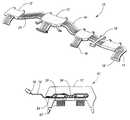
- FIG. 1is a view in perspective of a first exemplary automotive part incorporating overmolded, environmentally-sealed electronic assemblies in accordance with the invention
- FIG. 2is a plan view of the first exemplary part of FIG. 1 during its manufacture, wherein electronic components are mounted in a plurality of discrete groups on a first surface portion of a flexible substrate;
- FIG. 3is a plan view of the first exemplary part of FIG. 1 during its manufacture, wherein a suitable filler-material preform is positioned over each group of electronic components, and wherein a suitable adhesive is applied about the periphery of a second portion of the flexible circuit prior to folding the second portion over the first portion;
- FIG. 4is a plan view of the first exemplary part of FIG. 1 during its manufacture, wherein the second portion of the flexible circuit has been folded over the first portion such that the periphery of the second portion is sealingly attached to the first portion by the previously-applied adhesive;
- FIG. 5is a perspective view of a second exemplary automotive part incorporating an integrally-molded, environmentally-sealed electronic assembly in accordance with another feature of the invention
- FIG. 6is a cross-sectional view through the module of the electronic assembly shown in FIG. 5;
- FIG. 7is a perspective view of a third exemplary automotive part incorporating an integrally-molded, environmentally-sealed electronic assembly in accordance with another feature of the invention, along with an overlying protective cover;
- FIG. 8is a cross-sectional view through the module of the electronic assembly shown in FIG. 7 .
- FIGS. 1-4A first exemplary over-molded, environmentally-sealed electronic assembly 10 in accordance with the invention is illustrated in FIGS. 1-4.
- the first exemplary electronic assembly 10includes a plurality of circuit modules 12 that are linked together with suitable lengths of flexible circuit 14 .
- Certain modules 12include an additional length of flexible circuit 14 with a suitable terminal connector 16 .
- the first exemplary electronic assembly 10further includes an over-molded mounting structure 18 by which additional attachment points are defined on the electronic assembly 10 .
- the manufacture of the first exemplary electronic assembly 10begins with a thin, flexible substrate 20 wherein a first face 22 of the substrate 20 includes a pattern of electrically-connected traces 24 . At least one and, preferably, a plurality of electronic components 26 are mounted on the substrate's first face 22 in electrical interconnection with the conductive traces 24 to thereby define a plurality of component-populated portions 28 on the substrate 20 .
- a filler material 30preferably provided as a preform, is positioned over each component-populated portion 28 of the substrate 20 .
- the filler material 30is operative to neutralize a predetermined quantity of a penetrant to which the first exemplary electronic assembly 10 will be subjected in its normal service environment.
- the term “penetrant”is understood to encompass substances present in the surface environment which penetrate and/or permeate into the electronic assembly 10 over time; substances formed within the electronic assembly 10 as the result of such penetration and/or permeation of substance constituents; or the combination of either such substances or substance constituents with other constituents, e.g., process contaminants, which are internal to the electronic assembly 10 upon its manufacture.
- the flexible substrate 20advantageously includes a plurality of second portions 32 formed adjacent to the component-populated portions 28 which, as better shown in FIG. 4, can be conveniently folded over the component-populated portions 28 of the substrate 24 to thereby encapsulate both the electronic components 28 and the filler material 30 .
- the second, adjacent portions 32 of the substrate 20ultimately define a thin barrier member 34 which overlies each component-populated portion 28 of the electronic assembly 10 .
- the second, adjacent portions 32 of the substrate 20are correspondingly secured to component-populated portions 28 of the substrate 20 by a quantity of an adhesive material 36 that is applied between a peripheral portion 38 of the substrate's second portion 32 and a correspondingly-opposed portion 40 of the substrate's first face 22 .
- the inventioncontemplates any suitable mechanism for securing the second, adjacent portion 32 of the substrate 20 over its component-populated first portion 28 , including the use of heat-sealing coatings, dispensed or preform adhesives, or any other suitable process.
- the substrate's second, adjacent portion 32can be sealed to the opposed portion 40 on the substrate's first face 22 in a single step or, in the alternative, can be partially sealed to thereby create a contained enclosure within which filler material 30 may be inserted.
- Such an enclosureadvantageously permits use of powdered or other particulate filler material, as well as any foamed or liquid filler material.
- a relatively-rigid polymeric materialover-molded or insert-molded about or adjacent to the substrate 20 after the barrier members 34 have been sealingly attached to the substrate's upper face 22 , defines the assembly's several modules 12 and mounting structures 18 .
- the over-molded or insert-molded polymeric materialadvantageously provides the modules 12 of the resulting electronic assembly 10 with additional protection against damage from handling and installation.
- suitable materialsinclude thermoplastic resins, such as ABS (acrylonitrile-butadiene-styrene), Polypropylene (PP), and polyethylene (PE); polyesters such as Nylon (polyamide), and PEI (Polyetherimide); other polymer resins, such as thermosets and elastomeric resins, including epoxies, phenolics, and unsaturated polyesters; other thermosetting materials such as sheet molding compound, and thick molding compound; and other elastomers such as silicone, rubber, and polyurethane.
- thermoplastic resinssuch as ABS (acrylonitrile-butadiene-styrene), Polypropylene (PP), and polyethylene (PE); polyesters such as Nylon (polyamide), and PEI (Polyetherimide); other polymer resins, such as thermosets and elastomeric resins, including epoxies, phenolics, and unsaturated polyesters; other thermosetting materials such as sheet molding compound, and thick molding compound; and other
- the resulting over-molded modules 12provide rugged mechanical enclosures that may further serve to define one or more operative surfaces of the resulting assembly 10 .
- at least one of the assembly's molded modules 12advantageously defines operative surfaces and structures of a vehicle air duct panel 52 .
- Other suitable molded structuresinclude such functional housings as instrumental panel structures, door module cassettes or rear package trays (all not shown).
- the over-molded or insert-molded module 12may further include at least one heat sink 62 by which to facilitate the transfer of heat away from the assembly's electronic components 26 .
- the flexible substrate 20includes, as one of its lowermost layers, a metal foil layer 54 or other similar, highly-moisture-impervious foil or film, whereby the assembly's electronic components 26 and filler material 30 are fully encapsulated within a relatively moisture-impervious and, preferably, EMI-protective barrier.
- a metal foil layer 54 or filmthat is integrally formed within the substrate 20 or, alternatively, to which electronic circuitry 24 , 26 is otherwise adhesively bonded.
- the electronic circuitry 24 , 26is preferably bonded to the metal foil layer 54 with an electrically-insulative adhesive (not shown) to thereby electrically insulate the metal foil layer 54 from the substrate's electronic circuitry 24 , 26 .
- an insulating polymer film(also not shown) may be advantageously applied over the component-populated portion 28 of the substrate 20 prior to encapsulation to thereby avoid any deleterious electrical contact between the mounted components 26 and the barrier member's metal foil layer 54 .
- the filler material 30may be advantageously preformed to a predetermined shape characterized, for example, by a first side defining a plurality of recesses 56 within which to receive the mounted components 26 , and a second side defining a generally planar upper surface.
- a preformed filler material 30advantageously provides a relatively constant height to the resulting electronic assembly 50 while otherwise ensuring that the mounted electronic components 26 and, particularly, any frangible electrical interconnects between the electronic components 26 and the substrates electrically-conductive traces 24 , remain undisturbed in service.
- a substantially rigid preformed filler material 30also advantageously provides internal structural support for the electronic components 26 during the subsequent molding operations, during which external molding forces are exerted.
- dry air or an inert dry gaseous mediasuch as nitrogen is preferably used to purge and fill the module 12 during the sealing of the substrate's second, adjacent portions 32 to the substrate's upper face 22 .
- desecant fillerssuch as molecular sieves and vapor corrosion inhibitors.
- the filler material 30can alternatively be provided in powdered form, or as a high-viscous slurry such as an epoxy or polyurethane material that is applied over the component-populated portion 28 of the substrate 20 and cured prior to overlaying the barrier member 34 (e.g., the substrate's second, adjacent portions 32 ).
- the filler material 30is selected such that the filler material 30 is operative to neutralize a predetermined quantity of the penetrant.
- the filler material 30is preferably a corrosion-inhibiting material; and where the penetrant is moisture, the filler material 30 is preferably a desiccant.
- the inventionfurther contemplates the use of a filler material 30 which otherwise accommodates a further characteristic of the service environment in which the assembly is to be used. For example, where the service environment is characterized by the presence of a level of electromagnetic interference that is not otherwise accommodated by the assembly's encapsulating metal foil, the filler material advantageously further includes metallized particles.
- the inventioncontemplates use of any suitable filler material 30 , including solid- or liquid-phase materials, as well as those in either powdered or monolithic form.
- the substrate 20 and the barrier member 34together preferably define a pocket or enclosure for containing the filler material prior to sealingly attaching the barrier member to the substrate 20 .
- the barrier membermay alternatively be formed of a separate, thin member 58 which overlies the component-populated portions 28 of the substrate 20 .
- the separate member 58is otherwise preferably sealingly attached to the upper face 22 of the substrate 20 in a suitable manner, as through the use of an applied adhesive 59 .
Landscapes
- Engineering & Computer Science (AREA)
- Microelectronics & Electronic Packaging (AREA)
- Physics & Mathematics (AREA)
- Condensed Matter Physics & Semiconductors (AREA)
- General Physics & Mathematics (AREA)
- Computer Hardware Design (AREA)
- Power Engineering (AREA)
- Manufacturing & Machinery (AREA)
- Non-Metallic Protective Coatings For Printed Circuits (AREA)
- Structures Or Materials For Encapsulating Or Coating Semiconductor Devices Or Solid State Devices (AREA)
Abstract
Description
Claims (32)
Priority Applications (4)
| Application Number | Priority Date | Filing Date | Title |
|---|---|---|---|
| US09/578,394US6320128B1 (en) | 2000-05-25 | 2000-05-25 | Environmentally-sealed electronic assembly and method of making same |
| GB0201086AGB2369932B (en) | 2000-05-25 | 2001-05-25 | Environmentally-sealed electronic assembly and method of making same |
| DE10192115TDE10192115T1 (en) | 2000-05-25 | 2001-05-25 | Electronics construction sealed from the environment and method for its manufacture |
| PCT/US2001/017099WO2001091182A1 (en) | 2000-05-25 | 2001-05-25 | Environmentally-sealed electronic assembly and method of making same |
Applications Claiming Priority (1)
| Application Number | Priority Date | Filing Date | Title |
|---|---|---|---|
| US09/578,394US6320128B1 (en) | 2000-05-25 | 2000-05-25 | Environmentally-sealed electronic assembly and method of making same |
Publications (1)
| Publication Number | Publication Date |
|---|---|
| US6320128B1true US6320128B1 (en) | 2001-11-20 |
Family
ID=24312681
Family Applications (1)
| Application Number | Title | Priority Date | Filing Date |
|---|---|---|---|
| US09/578,394Expired - Fee RelatedUS6320128B1 (en) | 2000-05-25 | 2000-05-25 | Environmentally-sealed electronic assembly and method of making same |
Country Status (4)
| Country | Link |
|---|---|
| US (1) | US6320128B1 (en) |
| DE (1) | DE10192115T1 (en) |
| GB (1) | GB2369932B (en) |
| WO (1) | WO2001091182A1 (en) |
Cited By (25)
| Publication number | Priority date | Publication date | Assignee | Title |
|---|---|---|---|---|
| US6483713B2 (en)* | 2001-11-20 | 2002-11-19 | St. Jude Children's Research Hospital | Multilayered board comprising folded flexible circuits |
| US6487091B2 (en)* | 1999-09-28 | 2002-11-26 | Rockwell Automation Technologies, Inc. | Method and apparatus for supplying data and power to panel-supported components |
| WO2003045121A1 (en)* | 2001-11-20 | 2003-05-30 | St. Jude Children's Research Hospital | Multilayered board comprising folded flexible circuits and method of manufacture |
| US6770813B1 (en) | 2003-05-16 | 2004-08-03 | Visteon Global Technologies, Inc. | Mountable microelectronic package |
| US20040155021A1 (en)* | 2003-02-06 | 2004-08-12 | Norton David G. | Flexible heater for heating electrical components in operator control handle |
| WO2004091270A1 (en)* | 2003-04-03 | 2004-10-21 | Conti Temic Microelectronic Gmbh | Array for electrical connection |
| US6927344B1 (en) | 2004-02-27 | 2005-08-09 | Motorola, Inc. | Flexible circuit board assembly |
| US20060018098A1 (en)* | 2004-07-22 | 2006-01-26 | Adrian Hill | PCB board incorporating thermo-encapsulant for providing controlled heat dissipation and electromagnetic functions and associated method of manufacturing a PCB board |
| US20060097376A1 (en)* | 2002-08-05 | 2006-05-11 | Leurs Philip R | Electronic product, a body and a method of manufacturing |
| US20070091549A1 (en)* | 2005-10-26 | 2007-04-26 | Dell Products L.P. | Method and apparatus for mounting a component in a chassis |
| US20080128886A1 (en)* | 2006-11-30 | 2008-06-05 | Tessera, Inc. | Substrate for a flexible microelectronic assembly and a method of fabricating thereof |
| US20080188107A1 (en)* | 2007-02-01 | 2008-08-07 | Motorola, Inc. | Submersible electrical connector assembly and method of forming same |
| US20090073328A1 (en)* | 2007-09-07 | 2009-03-19 | Seagate Technology Llc | Liquid crystal material sealed housing |
| US20110007478A1 (en)* | 2009-07-10 | 2011-01-13 | Aisin Aw Co., Ltd. | Electronic circuit device |
| US20120066900A1 (en)* | 2005-11-29 | 2012-03-22 | Jeffrey Nall | Led lighting assemblies with thermal overmolding |
| US20190084505A1 (en)* | 2017-09-20 | 2019-03-21 | Yazaki Corporation | Conductor connection structure for routing members |
| US10345165B2 (en) | 2016-09-08 | 2019-07-09 | Covidien Lp | Force sensor for surgical devices |
| US10588231B2 (en) | 2017-05-18 | 2020-03-10 | Covidien Lp | Hermetically sealed printed circuit boards |
| US10667408B2 (en) | 2017-05-18 | 2020-05-26 | Covidien Lp | Fully encapsulated electronics and printed circuit boards |
| CN111418273A (en)* | 2017-12-12 | 2020-07-14 | 摩托罗拉移动有限责任公司 | Device component exposure protection |
| US10765428B2 (en) | 2016-08-15 | 2020-09-08 | Covidien Lp | Hermetic force sensors for surgical devices |
| US10973142B2 (en) | 2017-05-18 | 2021-04-06 | Covidien Lp | Hermetically sealed printed circuit boards |
| US11534086B2 (en) | 2020-10-30 | 2022-12-27 | Medtronic Minimed, Inc. | Low-profile wearable medical device |
| US12232771B2 (en) | 2021-06-10 | 2025-02-25 | Covidien Lp | Mechanical compression hermetic force sensors for surgical devices |
| US12342453B2 (en) | 2019-09-10 | 2025-06-24 | Innolux Corporation | ESD structure for a display substrate edge |
Families Citing this family (3)
| Publication number | Priority date | Publication date | Assignee | Title |
|---|---|---|---|---|
| DE102010062788A1 (en) | 2010-12-10 | 2012-06-14 | Robert Bosch Gmbh | Method for manufacturing electronic device for e.g. motor controller, in door of vehicle, involves fixing and hotly applying films on carrier by application of vacuum and fixed to electronics component by scrubbing at carrier |
| DE102015212169A1 (en)* | 2015-06-30 | 2017-01-05 | Osram Gmbh | Circuit carrier for an electronic circuit and method for producing such a circuit carrier |
| FR3148351A1 (en)* | 2023-04-26 | 2024-11-01 | Symbiose | Part comprising at least one electronic component covered by overmolding and at least one heat sink, method of manufacturing said part |
Citations (16)
| Publication number | Priority date | Publication date | Assignee | Title |
|---|---|---|---|---|
| US3909504A (en) | 1973-11-05 | 1975-09-30 | Carrier Tel Corp America Inc | Ruggedized package for electronic components and the like |
| US3999285A (en) | 1975-06-30 | 1976-12-28 | Burroughs Corporation | Semiconductor device package |
| US4409641A (en) | 1980-06-02 | 1983-10-11 | Robert Bosch Gmbh | Environmentally protected electronic network structure and housing combination |
| US4855867A (en) | 1987-02-02 | 1989-08-08 | International Business Machines Corporation | Full panel electronic packaging structure |
| US4961806A (en) | 1986-12-10 | 1990-10-09 | Sanders Associates, Inc. | Method of making a printed circuit |
| US4999741A (en) | 1988-01-26 | 1991-03-12 | The General Electric Company, P.L.C. | Package in the heat dissipation of Electronic devices |
| US5041943A (en) | 1989-11-06 | 1991-08-20 | Allied-Signal Inc. | Hermetically sealed printed circuit board |
| US5097390A (en) | 1986-12-10 | 1992-03-17 | Interflex Corporation | Printed circuit and fabrication of same |
| US5166864A (en) | 1991-05-17 | 1992-11-24 | Hughes Aircraft Company | Protected circuit card assembly and process |
| US5170326A (en) | 1990-02-05 | 1992-12-08 | Motorola, Inc. | Electronic module assembly |
| US5285559A (en) | 1992-09-10 | 1994-02-15 | Sundstrand Corporation | Method and apparatus for isolating electronic boards from shock and thermal environments |
| US5317478A (en) | 1991-11-12 | 1994-05-31 | Hughes Aircraft Company | Hermetic sealing of flexprint electronic packages |
| US5491300A (en)* | 1994-04-28 | 1996-02-13 | Cray Computer Corporation | Penetrator and flexible circuit assembly for sealed environment |
| US5584120A (en)* | 1992-02-14 | 1996-12-17 | Research Organization For Circuit Knowledge | Method of manufacturing printed circuits |
| US5655291A (en) | 1995-06-26 | 1997-08-12 | Ford Motor Company | Forming rigid circuit board |
| US6255949B1 (en)* | 1997-10-15 | 2001-07-03 | Escort Memory Systems | High temperature RFID tag |
Family Cites Families (3)
| Publication number | Priority date | Publication date | Assignee | Title |
|---|---|---|---|---|
| US5397921A (en)* | 1993-09-03 | 1995-03-14 | Advanced Semiconductor Assembly Technology | Tab grid array |
| TW258829B (en)* | 1994-01-28 | 1995-10-01 | Ibm | |
| US5844168A (en)* | 1995-08-01 | 1998-12-01 | Minnesota Mining And Manufacturing Company | Multi-layer interconnect sutructure for ball grid arrays |
- 2000
- 2000-05-25USUS09/578,394patent/US6320128B1/ennot_activeExpired - Fee Related
- 2001
- 2001-05-25DEDE10192115Tpatent/DE10192115T1/ennot_activeWithdrawn
- 2001-05-25WOPCT/US2001/017099patent/WO2001091182A1/enactiveApplication Filing
- 2001-05-25GBGB0201086Apatent/GB2369932B/ennot_activeExpired - Fee Related
Patent Citations (16)
| Publication number | Priority date | Publication date | Assignee | Title |
|---|---|---|---|---|
| US3909504A (en) | 1973-11-05 | 1975-09-30 | Carrier Tel Corp America Inc | Ruggedized package for electronic components and the like |
| US3999285A (en) | 1975-06-30 | 1976-12-28 | Burroughs Corporation | Semiconductor device package |
| US4409641A (en) | 1980-06-02 | 1983-10-11 | Robert Bosch Gmbh | Environmentally protected electronic network structure and housing combination |
| US4961806A (en) | 1986-12-10 | 1990-10-09 | Sanders Associates, Inc. | Method of making a printed circuit |
| US5097390A (en) | 1986-12-10 | 1992-03-17 | Interflex Corporation | Printed circuit and fabrication of same |
| US4855867A (en) | 1987-02-02 | 1989-08-08 | International Business Machines Corporation | Full panel electronic packaging structure |
| US4999741A (en) | 1988-01-26 | 1991-03-12 | The General Electric Company, P.L.C. | Package in the heat dissipation of Electronic devices |
| US5041943A (en) | 1989-11-06 | 1991-08-20 | Allied-Signal Inc. | Hermetically sealed printed circuit board |
| US5170326A (en) | 1990-02-05 | 1992-12-08 | Motorola, Inc. | Electronic module assembly |
| US5166864A (en) | 1991-05-17 | 1992-11-24 | Hughes Aircraft Company | Protected circuit card assembly and process |
| US5317478A (en) | 1991-11-12 | 1994-05-31 | Hughes Aircraft Company | Hermetic sealing of flexprint electronic packages |
| US5584120A (en)* | 1992-02-14 | 1996-12-17 | Research Organization For Circuit Knowledge | Method of manufacturing printed circuits |
| US5285559A (en) | 1992-09-10 | 1994-02-15 | Sundstrand Corporation | Method and apparatus for isolating electronic boards from shock and thermal environments |
| US5491300A (en)* | 1994-04-28 | 1996-02-13 | Cray Computer Corporation | Penetrator and flexible circuit assembly for sealed environment |
| US5655291A (en) | 1995-06-26 | 1997-08-12 | Ford Motor Company | Forming rigid circuit board |
| US6255949B1 (en)* | 1997-10-15 | 2001-07-03 | Escort Memory Systems | High temperature RFID tag |
Cited By (41)
| Publication number | Priority date | Publication date | Assignee | Title |
|---|---|---|---|---|
| US6487091B2 (en)* | 1999-09-28 | 2002-11-26 | Rockwell Automation Technologies, Inc. | Method and apparatus for supplying data and power to panel-supported components |
| US6795320B2 (en) | 1999-09-28 | 2004-09-21 | Rockwell Automation Technologies, Inc. | Method and apparatus for supplying data and power to panel-supported components |
| WO2003045121A1 (en)* | 2001-11-20 | 2003-05-30 | St. Jude Children's Research Hospital | Multilayered board comprising folded flexible circuits and method of manufacture |
| US6483713B2 (en)* | 2001-11-20 | 2002-11-19 | St. Jude Children's Research Hospital | Multilayered board comprising folded flexible circuits |
| US20060097376A1 (en)* | 2002-08-05 | 2006-05-11 | Leurs Philip R | Electronic product, a body and a method of manufacturing |
| US7563990B2 (en)* | 2002-08-05 | 2009-07-21 | Koninklijke Philips Electronics N.V. | Electronic product, a body and a method of manufacturing |
| US20040155021A1 (en)* | 2003-02-06 | 2004-08-12 | Norton David G. | Flexible heater for heating electrical components in operator control handle |
| US6900411B2 (en) | 2003-02-06 | 2005-05-31 | The Raymond Corporation | Flexible heater for heating electrical components in operator control handle |
| WO2004091270A1 (en)* | 2003-04-03 | 2004-10-21 | Conti Temic Microelectronic Gmbh | Array for electrical connection |
| US6770813B1 (en) | 2003-05-16 | 2004-08-03 | Visteon Global Technologies, Inc. | Mountable microelectronic package |
| US6927344B1 (en) | 2004-02-27 | 2005-08-09 | Motorola, Inc. | Flexible circuit board assembly |
| US20050190531A1 (en)* | 2004-02-27 | 2005-09-01 | Gall Thomas P. | Flexible circuit board assembly |
| US20060018098A1 (en)* | 2004-07-22 | 2006-01-26 | Adrian Hill | PCB board incorporating thermo-encapsulant for providing controlled heat dissipation and electromagnetic functions and associated method of manufacturing a PCB board |
| US20070091549A1 (en)* | 2005-10-26 | 2007-04-26 | Dell Products L.P. | Method and apparatus for mounting a component in a chassis |
| US7551433B2 (en)* | 2005-10-26 | 2009-06-23 | Dell Products L.P. | Method and apparatus for mounting a component in a chassis |
| US9585239B2 (en)* | 2005-11-29 | 2017-02-28 | GE Lighting Solutions, LLC | Methods of manufacturing lighting assembly with thermal overmolding |
| US20140237814A1 (en)* | 2005-11-29 | 2014-08-28 | Ge Lighting Solutions Llc | Led lighting assemblies with thermal overmolding |
| US8756801B2 (en)* | 2005-11-29 | 2014-06-24 | GE Lighting Solutions, LLC | Method of manufacturing a lighting assembly with thermal overmolding |
| US20120066900A1 (en)* | 2005-11-29 | 2012-03-22 | Jeffrey Nall | Led lighting assemblies with thermal overmolding |
| US7659617B2 (en) | 2006-11-30 | 2010-02-09 | Tessera, Inc. | Substrate for a flexible microelectronic assembly and a method of fabricating thereof |
| WO2008066894A3 (en)* | 2006-11-30 | 2008-08-14 | Tessera Inc | Substrate for a flexible microelectronic assembly |
| US20080128886A1 (en)* | 2006-11-30 | 2008-06-05 | Tessera, Inc. | Substrate for a flexible microelectronic assembly and a method of fabricating thereof |
| US7484981B2 (en)* | 2007-02-01 | 2009-02-03 | Motorola, Inc. | Assembly for sealing an audio connector within an electronic device |
| US20080188107A1 (en)* | 2007-02-01 | 2008-08-07 | Motorola, Inc. | Submersible electrical connector assembly and method of forming same |
| US8014167B2 (en)* | 2007-09-07 | 2011-09-06 | Seagate Technology Llc | Liquid crystal material sealed housing |
| US20090073328A1 (en)* | 2007-09-07 | 2009-03-19 | Seagate Technology Llc | Liquid crystal material sealed housing |
| US20110007478A1 (en)* | 2009-07-10 | 2011-01-13 | Aisin Aw Co., Ltd. | Electronic circuit device |
| US8169782B2 (en)* | 2009-07-10 | 2012-05-01 | Aisin Aw Co., Ltd. | Electronic circuit device |
| US10765428B2 (en) | 2016-08-15 | 2020-09-08 | Covidien Lp | Hermetic force sensors for surgical devices |
| US11571211B2 (en) | 2016-08-15 | 2023-02-07 | Covidien Lp | Hermetic force sensors for surgical devices |
| US10345165B2 (en) | 2016-09-08 | 2019-07-09 | Covidien Lp | Force sensor for surgical devices |
| US10648875B2 (en) | 2016-09-08 | 2020-05-12 | Covidien Lp | Force sensor for surgical devices |
| US10588231B2 (en) | 2017-05-18 | 2020-03-10 | Covidien Lp | Hermetically sealed printed circuit boards |
| US10667408B2 (en) | 2017-05-18 | 2020-05-26 | Covidien Lp | Fully encapsulated electronics and printed circuit boards |
| US10973142B2 (en) | 2017-05-18 | 2021-04-06 | Covidien Lp | Hermetically sealed printed circuit boards |
| US11304324B2 (en) | 2017-05-18 | 2022-04-12 | Covidien Lp | Hermetically sealed printed circuit boards |
| US20190084505A1 (en)* | 2017-09-20 | 2019-03-21 | Yazaki Corporation | Conductor connection structure for routing members |
| CN111418273A (en)* | 2017-12-12 | 2020-07-14 | 摩托罗拉移动有限责任公司 | Device component exposure protection |
| US12342453B2 (en) | 2019-09-10 | 2025-06-24 | Innolux Corporation | ESD structure for a display substrate edge |
| US11534086B2 (en) | 2020-10-30 | 2022-12-27 | Medtronic Minimed, Inc. | Low-profile wearable medical device |
| US12232771B2 (en) | 2021-06-10 | 2025-02-25 | Covidien Lp | Mechanical compression hermetic force sensors for surgical devices |
Also Published As
| Publication number | Publication date |
|---|---|
| WO2001091182A1 (en) | 2001-11-29 |
| GB0201086D0 (en) | 2002-03-06 |
| GB2369932B (en) | 2004-05-26 |
| GB2369932A (en) | 2002-06-12 |
| DE10192115T1 (en) | 2002-07-11 |
Similar Documents
| Publication | Publication Date | Title |
|---|---|---|
| US6320128B1 (en) | Environmentally-sealed electronic assembly and method of making same | |
| US9909946B2 (en) | Pressure sensor system | |
| US7118646B2 (en) | Method of manufacturing a sealed electronic module | |
| US8168896B2 (en) | Electronic housing | |
| CN100376868C (en) | inertial sensor | |
| JP6530498B2 (en) | Mechatronics component and method of manufacturing the same | |
| CN101107893A (en) | Control module | |
| JP5638088B2 (en) | Circuit module and method of manufacturing the circuit module | |
| CN1561574A (en) | Method for encapsulating an electrical component and surface wave component thus encapsulated | |
| KR102720829B1 (en) | A device for detecting the level of a medium | |
| CN1199252C (en) | Housing assembly for electronic component | |
| US6053049A (en) | Electrical device having atmospheric isolation | |
| US20080030973A1 (en) | Method for the production of a sensor and sensor | |
| KR102612671B1 (en) | Device for detecting the level of the medium | |
| WO1995019643A1 (en) | Improved low-cost package for electronic components | |
| US5714409A (en) | Method and apparatus for packaging a vehicle sensor and integrated circuit chip | |
| JP2003086722A (en) | Resin-sealed power module device | |
| US6956297B2 (en) | Electronic circuit unit that is easy to manufacture and method of manufacturing the same | |
| JP3620184B2 (en) | Pressure sensor | |
| CN113597542A (en) | Angle detection device | |
| EP3806142B1 (en) | Semiconductor module and method for producing the same | |
| JP2633285B2 (en) | In-vehicle hybrid integrated circuit device | |
| KR102076961B1 (en) | Encapsulated Electrical Device and Manufacturing Method | |
| US20230420271A1 (en) | Semiconductor power module and method for manufacturing a semiconductor power module for a semiconductor device and semiconductor device | |
| JPS59148841A (en) | Pressure sensor |
Legal Events
| Date | Code | Title | Description |
|---|---|---|---|
| AS | Assignment | Owner name:VISTEON GLOBAL TECHNOLOGIES, INC., MICHIGAN Free format text:ASSIGNMENT OF ASSIGNORS INTEREST;ASSIGNOR:FORD MOTOR COMPANY;REEL/FRAME:010968/0220 Effective date:20000615 | |
| AS | Assignment | Owner name:FORD MOTOR COMPANY, MICHIGAN Free format text:ASSIGNMENT OF ASSIGNORS INTEREST;ASSIGNORS:GLOVATSKY, ANDREW ZACHARY;NATION, BRENDA JOYCE;SCHWEITZER, CHARLES FREDERICK;AND OTHERS;REEL/FRAME:011300/0247;SIGNING DATES FROM 20000420 TO 20000518 | |
| FPAY | Fee payment | Year of fee payment:4 | |
| AS | Assignment | Owner name:JPMORGAN CHASE BANK, N.A., AS ADMINISTRATIVE AGENT Free format text:SECURITY AGREEMENT;ASSIGNOR:VISTEON GLOBAL TECHNOLOGIES, INC.;REEL/FRAME:020497/0733 Effective date:20060613 | |
| AS | Assignment | Owner name:JPMORGAN CHASE BANK, TEXAS Free format text:SECURITY INTEREST;ASSIGNOR:VISTEON GLOBAL TECHNOLOGIES, INC.;REEL/FRAME:022368/0001 Effective date:20060814 Owner name:JPMORGAN CHASE BANK,TEXAS Free format text:SECURITY INTEREST;ASSIGNOR:VISTEON GLOBAL TECHNOLOGIES, INC.;REEL/FRAME:022368/0001 Effective date:20060814 | |
| AS | Assignment | Owner name:WILMINGTON TRUST FSB, AS ADMINISTRATIVE AGENT, MIN Free format text:ASSIGNMENT OF SECURITY INTEREST IN PATENTS;ASSIGNOR:JPMORGAN CHASE BANK, N.A., AS ADMINISTRATIVE AGENT;REEL/FRAME:022575/0186 Effective date:20090415 Owner name:WILMINGTON TRUST FSB, AS ADMINISTRATIVE AGENT,MINN Free format text:ASSIGNMENT OF SECURITY INTEREST IN PATENTS;ASSIGNOR:JPMORGAN CHASE BANK, N.A., AS ADMINISTRATIVE AGENT;REEL/FRAME:022575/0186 Effective date:20090415 | |
| REMI | Maintenance fee reminder mailed | ||
| LAPS | Lapse for failure to pay maintenance fees | ||
| STCH | Information on status: patent discontinuation | Free format text:PATENT EXPIRED DUE TO NONPAYMENT OF MAINTENANCE FEES UNDER 37 CFR 1.362 | |
| FP | Lapsed due to failure to pay maintenance fee | Effective date:20091120 | |
| AS | Assignment | Owner name:VISTEON GLOBAL TECHNOLOGIES, INC., MICHIGAN Free format text:RELEASE BY SECURED PARTY AGAINST SECURITY INTEREST IN PATENTS RECORDED AT REEL 022575 FRAME 0186;ASSIGNOR:WILMINGTON TRUST FSB, AS ADMINISTRATIVE AGENT;REEL/FRAME:025105/0201 Effective date:20101001 |