US6319827B1 - Integrated electronic micromodule and method for making same - Google Patents
Integrated electronic micromodule and method for making sameDownload PDFInfo
- Publication number
- US6319827B1 US6319827B1US09/720,701US72070101AUS6319827B1US 6319827 B1US6319827 B1US 6319827B1US 72070101 AUS72070101 AUS 72070101AUS 6319827 B1US6319827 B1US 6319827B1
- Authority
- US
- United States
- Prior art keywords
- insulation layer
- coil
- integrated circuit
- electrical connector
- support wafer
- Prior art date
- Legal status (The legal status is an assumption and is not a legal conclusion. Google has not performed a legal analysis and makes no representation as to the accuracy of the status listed.)
- Expired - Lifetime
Links
Images


Classifications
- G—PHYSICS
- G06—COMPUTING OR CALCULATING; COUNTING
- G06K—GRAPHICAL DATA READING; PRESENTATION OF DATA; RECORD CARRIERS; HANDLING RECORD CARRIERS
- G06K19/00—Record carriers for use with machines and with at least a part designed to carry digital markings
- G06K19/06—Record carriers for use with machines and with at least a part designed to carry digital markings characterised by the kind of the digital marking, e.g. shape, nature, code
- G06K19/067—Record carriers with conductive marks, printed circuits or semiconductor circuit elements, e.g. credit or identity cards also with resonating or responding marks without active components
- G06K19/07—Record carriers with conductive marks, printed circuits or semiconductor circuit elements, e.g. credit or identity cards also with resonating or responding marks without active components with integrated circuit chips
- G06K19/077—Constructional details, e.g. mounting of circuits in the carrier
- G06K19/07745—Mounting details of integrated circuit chips
- G06K19/07747—Mounting details of integrated circuit chips at least one of the integrated circuit chips being mounted as a module
- G—PHYSICS
- G06—COMPUTING OR CALCULATING; COUNTING
- G06K—GRAPHICAL DATA READING; PRESENTATION OF DATA; RECORD CARRIERS; HANDLING RECORD CARRIERS
- G06K19/00—Record carriers for use with machines and with at least a part designed to carry digital markings
- G06K19/06—Record carriers for use with machines and with at least a part designed to carry digital markings characterised by the kind of the digital marking, e.g. shape, nature, code
- G06K19/067—Record carriers with conductive marks, printed circuits or semiconductor circuit elements, e.g. credit or identity cards also with resonating or responding marks without active components
- G06K19/07—Record carriers with conductive marks, printed circuits or semiconductor circuit elements, e.g. credit or identity cards also with resonating or responding marks without active components with integrated circuit chips
- G06K19/077—Constructional details, e.g. mounting of circuits in the carrier
- G06K19/07749—Constructional details, e.g. mounting of circuits in the carrier the record carrier being capable of non-contact communication, e.g. constructional details of the antenna of a non-contact smart card
- G06K19/0775—Constructional details, e.g. mounting of circuits in the carrier the record carrier being capable of non-contact communication, e.g. constructional details of the antenna of a non-contact smart card arrangements for connecting the integrated circuit to the antenna
- H—ELECTRICITY
- H01—ELECTRIC ELEMENTS
- H01L—SEMICONDUCTOR DEVICES NOT COVERED BY CLASS H10
- H01L23/00—Details of semiconductor or other solid state devices
- H01L23/48—Arrangements for conducting electric current to or from the solid state body in operation, e.g. leads, terminal arrangements ; Selection of materials therefor
- H01L23/488—Arrangements for conducting electric current to or from the solid state body in operation, e.g. leads, terminal arrangements ; Selection of materials therefor consisting of soldered or bonded constructions
- H01L23/498—Leads, i.e. metallisations or lead-frames on insulating substrates, e.g. chip carriers
- H01L23/49855—Leads, i.e. metallisations or lead-frames on insulating substrates, e.g. chip carriers for flat-cards, e.g. credit cards
- H—ELECTRICITY
- H01—ELECTRIC ELEMENTS
- H01L—SEMICONDUCTOR DEVICES NOT COVERED BY CLASS H10
- H01L23/00—Details of semiconductor or other solid state devices
- H01L23/58—Structural electrical arrangements for semiconductor devices not otherwise provided for, e.g. in combination with batteries
- H01L23/64—Impedance arrangements
- H01L23/645—Inductive arrangements
- H—ELECTRICITY
- H01—ELECTRIC ELEMENTS
- H01L—SEMICONDUCTOR DEVICES NOT COVERED BY CLASS H10
- H01L24/00—Arrangements for connecting or disconnecting semiconductor or solid-state bodies; Methods or apparatus related thereto
- H01L24/01—Means for bonding being attached to, or being formed on, the surface to be connected, e.g. chip-to-package, die-attach, "first-level" interconnects; Manufacturing methods related thereto
- H01L24/18—High density interconnect [HDI] connectors; Manufacturing methods related thereto
- H01L24/19—Manufacturing methods of high density interconnect preforms
- H—ELECTRICITY
- H01—ELECTRIC ELEMENTS
- H01L—SEMICONDUCTOR DEVICES NOT COVERED BY CLASS H10
- H01L24/00—Arrangements for connecting or disconnecting semiconductor or solid-state bodies; Methods or apparatus related thereto
- H01L24/80—Methods for connecting semiconductor or other solid state bodies using means for bonding being attached to, or being formed on, the surface to be connected
- H01L24/82—Methods for connecting semiconductor or other solid state bodies using means for bonding being attached to, or being formed on, the surface to be connected by forming build-up interconnects at chip-level, e.g. for high density interconnects [HDI]
- H—ELECTRICITY
- H04—ELECTRIC COMMUNICATION TECHNIQUE
- H04B—TRANSMISSION
- H04B5/00—Near-field transmission systems, e.g. inductive or capacitive transmission systems
- H04B5/20—Near-field transmission systems, e.g. inductive or capacitive transmission systems characterised by the transmission technique; characterised by the transmission medium
- H04B5/24—Inductive coupling
- H04B5/26—Inductive coupling using coils
- H04B5/263—Multiple coils at either side
- H—ELECTRICITY
- H01—ELECTRIC ELEMENTS
- H01L—SEMICONDUCTOR DEVICES NOT COVERED BY CLASS H10
- H01L2223/00—Details relating to semiconductor or other solid state devices covered by the group H01L23/00
- H01L2223/58—Structural electrical arrangements for semiconductor devices not otherwise provided for
- H01L2223/64—Impedance arrangements
- H01L2223/66—High-frequency adaptations
- H01L2223/6661—High-frequency adaptations for passive devices
- H01L2223/6677—High-frequency adaptations for passive devices for antenna, e.g. antenna included within housing of semiconductor device
- H—ELECTRICITY
- H01—ELECTRIC ELEMENTS
- H01L—SEMICONDUCTOR DEVICES NOT COVERED BY CLASS H10
- H01L2224/00—Indexing scheme for arrangements for connecting or disconnecting semiconductor or solid-state bodies and methods related thereto as covered by H01L24/00
- H01L2224/01—Means for bonding being attached to, or being formed on, the surface to be connected, e.g. chip-to-package, die-attach, "first-level" interconnects; Manufacturing methods related thereto
- H01L2224/02—Bonding areas; Manufacturing methods related thereto
- H01L2224/04—Structure, shape, material or disposition of the bonding areas prior to the connecting process
- H01L2224/04105—Bonding areas formed on an encapsulation of the semiconductor or solid-state body, e.g. bonding areas on chip-scale packages
- H—ELECTRICITY
- H01—ELECTRIC ELEMENTS
- H01L—SEMICONDUCTOR DEVICES NOT COVERED BY CLASS H10
- H01L2224/00—Indexing scheme for arrangements for connecting or disconnecting semiconductor or solid-state bodies and methods related thereto as covered by H01L24/00
- H01L2224/01—Means for bonding being attached to, or being formed on, the surface to be connected, e.g. chip-to-package, die-attach, "first-level" interconnects; Manufacturing methods related thereto
- H01L2224/18—High density interconnect [HDI] connectors; Manufacturing methods related thereto
- H—ELECTRICITY
- H01—ELECTRIC ELEMENTS
- H01L—SEMICONDUCTOR DEVICES NOT COVERED BY CLASS H10
- H01L2224/00—Indexing scheme for arrangements for connecting or disconnecting semiconductor or solid-state bodies and methods related thereto as covered by H01L24/00
- H01L2224/01—Means for bonding being attached to, or being formed on, the surface to be connected, e.g. chip-to-package, die-attach, "first-level" interconnects; Manufacturing methods related thereto
- H01L2224/26—Layer connectors, e.g. plate connectors, solder or adhesive layers; Manufacturing methods related thereto
- H01L2224/31—Structure, shape, material or disposition of the layer connectors after the connecting process
- H01L2224/32—Structure, shape, material or disposition of the layer connectors after the connecting process of an individual layer connector
- H01L2224/321—Disposition
- H01L2224/32151—Disposition the layer connector connecting between a semiconductor or solid-state body and an item not being a semiconductor or solid-state body, e.g. chip-to-substrate, chip-to-passive
- H01L2224/32221—Disposition the layer connector connecting between a semiconductor or solid-state body and an item not being a semiconductor or solid-state body, e.g. chip-to-substrate, chip-to-passive the body and the item being stacked
- H01L2224/32225—Disposition the layer connector connecting between a semiconductor or solid-state body and an item not being a semiconductor or solid-state body, e.g. chip-to-substrate, chip-to-passive the body and the item being stacked the item being non-metallic, e.g. insulating substrate with or without metallisation
- H—ELECTRICITY
- H01—ELECTRIC ELEMENTS
- H01L—SEMICONDUCTOR DEVICES NOT COVERED BY CLASS H10
- H01L2224/00—Indexing scheme for arrangements for connecting or disconnecting semiconductor or solid-state bodies and methods related thereto as covered by H01L24/00
- H01L2224/01—Means for bonding being attached to, or being formed on, the surface to be connected, e.g. chip-to-package, die-attach, "first-level" interconnects; Manufacturing methods related thereto
- H01L2224/42—Wire connectors; Manufacturing methods related thereto
- H01L2224/44—Structure, shape, material or disposition of the wire connectors prior to the connecting process
- H01L2224/45—Structure, shape, material or disposition of the wire connectors prior to the connecting process of an individual wire connector
- H01L2224/45001—Core members of the connector
- H01L2224/45099—Material
- H01L2224/451—Material with a principal constituent of the material being a metal or a metalloid, e.g. boron (B), silicon (Si), germanium (Ge), arsenic (As), antimony (Sb), tellurium (Te) and polonium (Po), and alloys thereof
- H01L2224/45117—Material with a principal constituent of the material being a metal or a metalloid, e.g. boron (B), silicon (Si), germanium (Ge), arsenic (As), antimony (Sb), tellurium (Te) and polonium (Po), and alloys thereof the principal constituent melting at a temperature of greater than or equal to 400°C and less than 950°C
- H01L2224/45124—Aluminium (Al) as principal constituent
- H—ELECTRICITY
- H01—ELECTRIC ELEMENTS
- H01L—SEMICONDUCTOR DEVICES NOT COVERED BY CLASS H10
- H01L2224/00—Indexing scheme for arrangements for connecting or disconnecting semiconductor or solid-state bodies and methods related thereto as covered by H01L24/00
- H01L2224/01—Means for bonding being attached to, or being formed on, the surface to be connected, e.g. chip-to-package, die-attach, "first-level" interconnects; Manufacturing methods related thereto
- H01L2224/42—Wire connectors; Manufacturing methods related thereto
- H01L2224/44—Structure, shape, material or disposition of the wire connectors prior to the connecting process
- H01L2224/45—Structure, shape, material or disposition of the wire connectors prior to the connecting process of an individual wire connector
- H01L2224/45001—Core members of the connector
- H01L2224/45099—Material
- H01L2224/451—Material with a principal constituent of the material being a metal or a metalloid, e.g. boron (B), silicon (Si), germanium (Ge), arsenic (As), antimony (Sb), tellurium (Te) and polonium (Po), and alloys thereof
- H01L2224/45138—Material with a principal constituent of the material being a metal or a metalloid, e.g. boron (B), silicon (Si), germanium (Ge), arsenic (As), antimony (Sb), tellurium (Te) and polonium (Po), and alloys thereof the principal constituent melting at a temperature of greater than or equal to 950°C and less than 1550°C
- H01L2224/45144—Gold (Au) as principal constituent
- H—ELECTRICITY
- H01—ELECTRIC ELEMENTS
- H01L—SEMICONDUCTOR DEVICES NOT COVERED BY CLASS H10
- H01L2224/00—Indexing scheme for arrangements for connecting or disconnecting semiconductor or solid-state bodies and methods related thereto as covered by H01L24/00
- H01L2224/01—Means for bonding being attached to, or being formed on, the surface to be connected, e.g. chip-to-package, die-attach, "first-level" interconnects; Manufacturing methods related thereto
- H01L2224/42—Wire connectors; Manufacturing methods related thereto
- H01L2224/44—Structure, shape, material or disposition of the wire connectors prior to the connecting process
- H01L2224/45—Structure, shape, material or disposition of the wire connectors prior to the connecting process of an individual wire connector
- H01L2224/45001—Core members of the connector
- H01L2224/45099—Material
- H01L2224/451—Material with a principal constituent of the material being a metal or a metalloid, e.g. boron (B), silicon (Si), germanium (Ge), arsenic (As), antimony (Sb), tellurium (Te) and polonium (Po), and alloys thereof
- H01L2224/45138—Material with a principal constituent of the material being a metal or a metalloid, e.g. boron (B), silicon (Si), germanium (Ge), arsenic (As), antimony (Sb), tellurium (Te) and polonium (Po), and alloys thereof the principal constituent melting at a temperature of greater than or equal to 950°C and less than 1550°C
- H01L2224/45147—Copper (Cu) as principal constituent
- H—ELECTRICITY
- H01—ELECTRIC ELEMENTS
- H01L—SEMICONDUCTOR DEVICES NOT COVERED BY CLASS H10
- H01L2224/00—Indexing scheme for arrangements for connecting or disconnecting semiconductor or solid-state bodies and methods related thereto as covered by H01L24/00
- H01L2224/73—Means for bonding being of different types provided for in two or more of groups H01L2224/10, H01L2224/18, H01L2224/26, H01L2224/34, H01L2224/42, H01L2224/50, H01L2224/63, H01L2224/71
- H01L2224/732—Location after the connecting process
- H01L2224/73251—Location after the connecting process on different surfaces
- H01L2224/73267—Layer and HDI connectors
- H—ELECTRICITY
- H01—ELECTRIC ELEMENTS
- H01L—SEMICONDUCTOR DEVICES NOT COVERED BY CLASS H10
- H01L2224/00—Indexing scheme for arrangements for connecting or disconnecting semiconductor or solid-state bodies and methods related thereto as covered by H01L24/00
- H01L2224/91—Methods for connecting semiconductor or solid state bodies including different methods provided for in two or more of groups H01L2224/80 - H01L2224/90
- H01L2224/92—Specific sequence of method steps
- H01L2224/922—Connecting different surfaces of the semiconductor or solid-state body with connectors of different types
- H01L2224/9222—Sequential connecting processes
- H01L2224/92242—Sequential connecting processes the first connecting process involving a layer connector
- H01L2224/92244—Sequential connecting processes the first connecting process involving a layer connector the second connecting process involving a build-up interconnect
- H—ELECTRICITY
- H01—ELECTRIC ELEMENTS
- H01L—SEMICONDUCTOR DEVICES NOT COVERED BY CLASS H10
- H01L2924/00—Indexing scheme for arrangements or methods for connecting or disconnecting semiconductor or solid-state bodies as covered by H01L24/00
- H01L2924/01—Chemical elements
- H01L2924/01005—Boron [B]
- H—ELECTRICITY
- H01—ELECTRIC ELEMENTS
- H01L—SEMICONDUCTOR DEVICES NOT COVERED BY CLASS H10
- H01L2924/00—Indexing scheme for arrangements or methods for connecting or disconnecting semiconductor or solid-state bodies as covered by H01L24/00
- H01L2924/01—Chemical elements
- H01L2924/01006—Carbon [C]
- H—ELECTRICITY
- H01—ELECTRIC ELEMENTS
- H01L—SEMICONDUCTOR DEVICES NOT COVERED BY CLASS H10
- H01L2924/00—Indexing scheme for arrangements or methods for connecting or disconnecting semiconductor or solid-state bodies as covered by H01L24/00
- H01L2924/01—Chemical elements
- H01L2924/01013—Aluminum [Al]
- H—ELECTRICITY
- H01—ELECTRIC ELEMENTS
- H01L—SEMICONDUCTOR DEVICES NOT COVERED BY CLASS H10
- H01L2924/00—Indexing scheme for arrangements or methods for connecting or disconnecting semiconductor or solid-state bodies as covered by H01L24/00
- H01L2924/01—Chemical elements
- H01L2924/01015—Phosphorus [P]
- H—ELECTRICITY
- H01—ELECTRIC ELEMENTS
- H01L—SEMICONDUCTOR DEVICES NOT COVERED BY CLASS H10
- H01L2924/00—Indexing scheme for arrangements or methods for connecting or disconnecting semiconductor or solid-state bodies as covered by H01L24/00
- H01L2924/01—Chemical elements
- H01L2924/01029—Copper [Cu]
- H—ELECTRICITY
- H01—ELECTRIC ELEMENTS
- H01L—SEMICONDUCTOR DEVICES NOT COVERED BY CLASS H10
- H01L2924/00—Indexing scheme for arrangements or methods for connecting or disconnecting semiconductor or solid-state bodies as covered by H01L24/00
- H01L2924/01—Chemical elements
- H01L2924/01033—Arsenic [As]
- H—ELECTRICITY
- H01—ELECTRIC ELEMENTS
- H01L—SEMICONDUCTOR DEVICES NOT COVERED BY CLASS H10
- H01L2924/00—Indexing scheme for arrangements or methods for connecting or disconnecting semiconductor or solid-state bodies as covered by H01L24/00
- H01L2924/01—Chemical elements
- H01L2924/01046—Palladium [Pd]
- H—ELECTRICITY
- H01—ELECTRIC ELEMENTS
- H01L—SEMICONDUCTOR DEVICES NOT COVERED BY CLASS H10
- H01L2924/00—Indexing scheme for arrangements or methods for connecting or disconnecting semiconductor or solid-state bodies as covered by H01L24/00
- H01L2924/01—Chemical elements
- H01L2924/01058—Cerium [Ce]
- H—ELECTRICITY
- H01—ELECTRIC ELEMENTS
- H01L—SEMICONDUCTOR DEVICES NOT COVERED BY CLASS H10
- H01L2924/00—Indexing scheme for arrangements or methods for connecting or disconnecting semiconductor or solid-state bodies as covered by H01L24/00
- H01L2924/01—Chemical elements
- H01L2924/01079—Gold [Au]
- H—ELECTRICITY
- H01—ELECTRIC ELEMENTS
- H01L—SEMICONDUCTOR DEVICES NOT COVERED BY CLASS H10
- H01L2924/00—Indexing scheme for arrangements or methods for connecting or disconnecting semiconductor or solid-state bodies as covered by H01L24/00
- H01L2924/01—Chemical elements
- H01L2924/01082—Lead [Pb]
- H—ELECTRICITY
- H01—ELECTRIC ELEMENTS
- H01L—SEMICONDUCTOR DEVICES NOT COVERED BY CLASS H10
- H01L2924/00—Indexing scheme for arrangements or methods for connecting or disconnecting semiconductor or solid-state bodies as covered by H01L24/00
- H01L2924/10—Details of semiconductor or other solid state devices to be connected
- H01L2924/102—Material of the semiconductor or solid state bodies
- H01L2924/1025—Semiconducting materials
- H01L2924/10251—Elemental semiconductors, i.e. Group IV
- H01L2924/10253—Silicon [Si]
- H—ELECTRICITY
- H01—ELECTRIC ELEMENTS
- H01L—SEMICONDUCTOR DEVICES NOT COVERED BY CLASS H10
- H01L2924/00—Indexing scheme for arrangements or methods for connecting or disconnecting semiconductor or solid-state bodies as covered by H01L24/00
- H01L2924/10—Details of semiconductor or other solid state devices to be connected
- H01L2924/11—Device type
- H01L2924/14—Integrated circuits
- H—ELECTRICITY
- H01—ELECTRIC ELEMENTS
- H01L—SEMICONDUCTOR DEVICES NOT COVERED BY CLASS H10
- H01L2924/00—Indexing scheme for arrangements or methods for connecting or disconnecting semiconductor or solid-state bodies as covered by H01L24/00
- H01L2924/19—Details of hybrid assemblies other than the semiconductor or other solid state devices to be connected
- H01L2924/1901—Structure
- H01L2924/1904—Component type
- H01L2924/19042—Component type being an inductor
- H—ELECTRICITY
- H01—ELECTRIC ELEMENTS
- H01L—SEMICONDUCTOR DEVICES NOT COVERED BY CLASS H10
- H01L2924/00—Indexing scheme for arrangements or methods for connecting or disconnecting semiconductor or solid-state bodies as covered by H01L24/00
- H01L2924/30—Technical effects
- H01L2924/301—Electrical effects
- H01L2924/30105—Capacitance
- H—ELECTRICITY
- H01—ELECTRIC ELEMENTS
- H01L—SEMICONDUCTOR DEVICES NOT COVERED BY CLASS H10
- H01L2924/00—Indexing scheme for arrangements or methods for connecting or disconnecting semiconductor or solid-state bodies as covered by H01L24/00
- H01L2924/30—Technical effects
- H01L2924/301—Electrical effects
- H01L2924/30107—Inductance
- H—ELECTRICITY
- H01—ELECTRIC ELEMENTS
- H01L—SEMICONDUCTOR DEVICES NOT COVERED BY CLASS H10
- H01L2924/00—Indexing scheme for arrangements or methods for connecting or disconnecting semiconductor or solid-state bodies as covered by H01L24/00
- H01L2924/30—Technical effects
- H01L2924/301—Electrical effects
- H01L2924/3025—Electromagnetic shielding
Definitions
- the present inventionrelates to electronics, and, more particularly, to an electronic micromodule comprising a support wafer, an integrated circuit chip, and at least one flat winding forming an antenna coil.
- contactless integrated circuitshave been developed that operate through an antenna coil, including receiving or transmitting data by inductive coupling in the presence of a magnetic field transmitted by a data transmitting and/or receiving station.
- These integrated circuitswhich are also called passive transponders, can be used to produce various contactless electronic portable objects such as smart cards, electronic tags and electronic tokens, for example.
- the present inventionconcerns the production of such portable objects, and, more particularly, the production of the electronic part of such objects.
- the most frequently used method to produce the electronic part of a contactless portable objectincludes using a support wafer on which a coil and a silicon chip are arranged. The coil is then connected to the chip and the unit is covered with protective resin.
- the support waferis a printed circuit board.
- the coilis a copper wire glued on or an etched copper strip.
- the coil and chipare connected by ultrasonically bonded metal wires.
- the assemblyforms an electronic micromodule designed to be inserted into the body of a portable object (plastic card, token, land, key . . . ) or fixed onto the surface of such an object.
- the printed circuit boardis approximately 150 micrometers thick
- the silicon chipis approximately 150 micrometers thick once the rear side has been chemically or mechanically abraded
- the height of the loops formed by the wiring cablesis in the region of 120 micrometers.
- the thickness of the resin coating the wiresis between 20 and 50 micrometers.
- the thickness of a classic micromoduleis in the region of 400 to 500 micrometers.
- the thickness of a plastic cardis approximately 760 micrometers. Contactless smart cards that contain this type of micromodule are often uneven.
- the surface area provided by a silicon chipwhich is a few square millimeters, is insufficient to produce a high inductance coil.
- Integrated circuits fitted with an integrated coilare therefore reserved for so-called “proximity” applications. This is where the electromagnetic induction communication distance is short, and is on the order of one millimeter.
- An object of the present inventionis to provide a method to manufacture thin micromodules together that comprise an integrated coil and an integrated circuit, without increasing the cost price of integrated circuits and without the need to assemble individual components.
- Another object of the present inventionis to provide a hybrid micromodule with two operating modes, one conventional operating mode via contact pads and one contactless operating mode via an antenna coil that is small in size and easy to produce.
- a collective manufacturing method for a plurality of electronic micromoduleseach comprising a support wafer, an integrated circuit chip with electric connector areas, and at least one coil.
- the methodcomprises assembling a plurality of integrated circuit chips onto a support wafer; depositing on the surface of the support wafer an electrically insulating layer covering all the chips; making several apertures in the insulating layer opposite the connector areas of the chips; jointly producing on the support wafer a plurality of flat windings forming coils; connecting each coil to a corresponding chip; and cutting out the support wafer to separate the micromodules.
- the coilsare connected to the chips by depositing a conducting material in the apertures made in the insulating layer.
- the conducting material deposited in the aperturesis the conducting material forming the coils.
- the coilis produced on several conducting levels separated by insulating layers.
- the support waferis made of silicon.
- the deposit of an insulating layerincludes one step of depositing a layer of polyimide and one step of depositing a layer of silicon dioxide.
- the coilsare produced by copper electroplating.
- a protective materialis deposited on the entire support wafer before cutting the support wafer.
- the present inventionalso concerns an electronic micromodule comprising a support wafer, an integrated circuit chip and at least one flat winding forming a coil.
- the chipis preferably embedded in at least one electrically insulating layer comprising at least one layer of at least one insulating material, and the coil is arranged on the insulating layer.
- the coilis preferably connected to the chip through metal apertures passing through the insulating layer to reach the electric connector areas of the chip.
- the chipis covered with at least two insulating layers, one of the two insulating layers is a support for the winding forming the coil.
- the other insulating layeris a support for a conductor linking one end of the coil to a connector area of the chip.
- the chipis covered with at least two insulating layers and the coil comprises at least two flat windings arranged respectively on each of the insulating layers.
- the present inventionalso concerns a hybrid micromodule comprising a support wafer with contact pads on its front side, and in which the support wafer has a micromodule according to the present invention on the rear side.
- the micromodulepreferably comprises an integrated circuit chip with two operating modes, with or without contact, and an insulating layer with apertures to connect the chip to the contact pads.
- FIGS. 1 and 2respectively illustrate a top view and a sectional view of a support wafer on which silicon chips are deposited, and illustrates an initial step of the method according to the present invention
- FIGS. 3A to 3 Dare partial sectional views of the support wafer and illustrate other steps of the method according to the present invention.
- FIG. 4is a top view of an initial example of the production of micromodules according to the present invention.
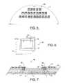
- FIG. 5is a general view of a plurality of micromodules produced together on the support wafer according to the present invention.
- FIGS. 6 and 7respectively represent a top view and a sectional view of a second example of the production of a micromodule according to the present invention
- FIGS. 8 and 9respectively represent a top view and a sectional view of a third example of the production of a micromodule according to the present invention.
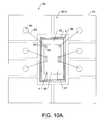
- FIGS. 10A and 10Brespectively represent a bottom view and a top view of a hybrid micromodule comprising a micromodule and contact pads according to the present invention.
- FIG. 11is a wiring diagram in block form of a contactless integrated circuit and a data transmitting/receiving station according to the present invention.
- the idea of the present inventionis to produce coils together on a support on which integrated circuit chips have previously been arranged.
- the supportis different from the silicon wafer used to manufacture the integrated circuits, and the method does not increase the cost of such.
- the coilsare produced by using low-cost technology. Thus, after cutting out the support, integrated micromodules are produced at a low cost.
- An initial step of the method according to the inventionincludes arranging a plurality of silicon chips 1 on a support wafer 2 that is preferably rigid.
- the chipsare fixed onto the support wafer 2 by any classic method, such as gluing, for example, and are arranged at a predetermined distance D from each other.
- This stepis preferably automated so that the chips are precisely positioned.
- patterns 3can be used on the support wafer 2 .
- the silicon chips 1are contactless type integrated circuits comprising metal pads 4 to be connected to a coil.
- the chipsare made out of a silicon wafer pared by a classic chemical or mechanical abrasion method.
- the thickness of the chipsmay be less than that of chips mounted onto printed circuit boards due to the rigidity of the support wafer 2 , and may be on the order of 50 to 150 micrometers.
- the support wafer 2on the support wafer 2 a plurality of integrated coils are produced to form thin integrated micromodules with the chips 1 .
- An example of implementation of the method according to the inventionis described below using polyimide/silicon dioxide/copper technology on a silicon substrate, as used in the prior art to produce integrated coils.
- the support wafer 2is a blank silicon wafer of standard thickness in the region of 675 micrometers that will be pared during a final step of the manufacturing method.
- FIGS. 3A to 3 Care partial sectional views of the support wafer 2 illustrating various steps of the method according to the invention. The thickness of the various elements is not reproduced to scale so that the diagrams remain legible.
- the support wafer 2is coated with a layer 5 of polyimide.
- the polyimideis deposited in liquid form, then spread over the wafer 2 by centrifugation and polymerized in a drying oven. Depending on the viscosity of the polyimide, several depositing, centrifugation and polymerization steps may be required to obtain a layer 5 that fully covers the silicon chips 1 .
- This stepis followed by a traditional resurfacing step (planarizing) of the polyimide layer 5 , such as by mechanical abrasion, for example.
- a traditional resurfacing stepplanarizing of the polyimide layer 5 , such as by mechanical abrasion, for example.
- the mechanical abrasionis be continued until the thickness of the polyimide layer 5 over the silicon chips 1 is quite low, such as in region of 10 micrometers, for example.
- the following stepinvolves depositing a fine layer of silicon dioxide 6 having a thickness in the region of 5 to 10 micrometers on the resurfaced area 5 .
- the silicon dioxideis deposited using a classic method, such as during a vapor phase using a chemical vapor deposition (CVD) technique, for example.
- CVDchemical vapor deposition
- the layers of polyimide 5 and silicon dioxide 6form a single insulating layer 7 in which the chip 1 is embedded.
- the cumulated deposit of these two materialsis a particular feature of the method used here, as the polyimide allows a thick insulating layer to be produced in a short space of time.
- the silicon dioxideis used as a support for a layer of copper deposited during a step described below.
- the insulating layer 7is perforated to make apertures 8 opposite the metal pads 4 of silicon chips 1 .
- apertures 8are produced by chemically etching the insulating layer 7 using a photosensitive etching resist that has first been insulated and developed.
- a photosensitive etching resistthat has first been insulated and developed.
- One particular approach to this etching phaseincludes etching the layer of silicon dioxide 6 first using an etchant that is non-aggressive for the polyimide, with interposition of an etching resist. Then, the etched layer of silicon dioxide is used as an etching resist to etch the layer of polyimide 5 using a second etchant that is non-aggressive for the silicon dioxide.
- a layer of copper 9 having a thickness of approximately 20 to 50 micrometersis deposited on the insulating layer 7 by electroplating, for example.
- the layer of copper 9penetrates into the apertures 8 and adheres to the connector areas 4 of the chip 1 .
- the layer of copper 9is then etched so that the flat windings in the form of coils 10 appear, with each winding connected to a silicon chip 1 .
- FIG. 4represents an example of a coil 10 produced according to the method of the invention method, wherein an integrated micromodule 20 is illustrated as having an embedded chip 1 therein.
- the coil 10overlaps the chip 1 in a considerably offset position allowing the ends of the inner turn and the outer turn to coincide with the connector areas 4 of the chip 1 .
- FIG. 5gives an overall view of the surface of the silicon wafer 2 . It shows that a plurality of micromodules 20 have been produced together. Before being cut into separate micromodules, wafer 2 is preferably coated with a layer of protective resin, then pared by abrasion of the rear side until a thickness in the region of 100 micrometers is obtained. At the end, the micromodules according to the invention are approximately 200 to 300 micrometers thick.
- the method according to the present inventionit is possible to produce integrated micromodules that are comparable in terms of size to those produced in the prior art on silicon wafers comprising integrated circuits.
- the surface occupied by the coilschosen according to the intended application, does not affect the cost of the integrated circuits that are produced here on an independent silicon wafer.
- the manufacturing method of the coilsis much less expensive than the manufacturing method of the integrated circuits, the cost of micromodules according to the invention does not increase in an unacceptable manner according to the surface area occupied by the coils.
- the production of a micromodule according to the inventiononly requires, in practice, 2 to 5 etching resists (depending on the embodiment chosen) while the manufacture of an integrated circuit usually requires about twenty etching resists.
- the precision required to produce the coilsis only in the region of 1 to 2 micrometers while integrated circuits are currently produced with a precision of less than a micrometer.
- the method according to the inventionoffers extensive possibilities in terms of micromodule design due to the possibility of having several conducting levels.
- several levels of copperare separated by insulating layers.
- several conducting levelscan be used to reduce the number of coil windings.
- a compromisecan be achieved between an extension of the number of windings in the plane of the support wafer and an extension of the number of windings over several conducting levels.
- FIGS. 6-7 and 8 - 9represent two other examples of the production of micromodules according to the invention.
- the micromodule 30 shown in FIGS. 6 and 7comprises a coil 31 that is larger than that of the micromodule shown in FIG. 4, and here the coil 31 surrounds the silicon chip 1 .
- the outer turn of the coil 31is connected to one of the metal pads 4 of the silicon chip by a conductor 32 in copper arranged on an initial insulating layer 33 , with the coil 31 arranged on a second insulating layer 34 .
- the conductor 32is connected to the coil 31 through an aperture 35 made in layer 34 and it is connected to the metal pad 4 through an aperture 36 made in layer 33 . Finally, the internal turn of the coil 31 is connected to the other metal pad 4 through two superimposed apertures 37 and 38 made in insulating layers 33 and 34 .
- One embodimentinverts the relative positions of the coil 31 and the conductor 32 on each of the insulating layers.
- Micromodule 40 represented in FIGS. 8 and 9comprises two insulating layers 41 , 42 and a coil 43 with two flat windings 44 , 45 that are superimposed and connected in series.
- the first winding 44represented by a dotted line in FIG. 8, is deposited on the insulating layer 41 .
- One of its endsis connected to a metal pad 4 of the chip 1 through an aperture 46 made in the first insulating layer 41 .
- the other end of the winding 44is connected to one end of the second winding 45 through an aperture 47 made in the second insulating layer 42 .
- the other end of winding 45is connected to the other metal pad 4 of the chip 1 through two superimposed apertures 48 , 49 made in the two insulating layers 41 , 42 .
- FIGS. 10A and 10Brespectively show the rear side 60 - 1 and the front 60 - 2 of a hybrid micromodule 60 for a smart card with two operating modes.
- Micromodule 60comprises a thin support wafer 61 , such as an epoxy wafer, for example.
- a micromodule 50 according to the invention of the type described in relation with FIGS. 6 or 8comprising a support wafer 2 and a coil 51 surrounding a silicon chip 52 embedded in an insulating layer 53 is stuck onto the rear side 60 - 1 of the wafer 61 .
- the coil 51produced on two first levels of insulating layer 53 , is covered with a third level of the insulating layer 53 and/or by protective resin.
- the silicon chip 52is an integrated circuit with two operating modes of a well-known type, such as, for example, the one described in the European Application WO 97/49059.
- the chip 52comprises two metal pads 4 connected to a coil 51 for contactless operation, and metal pads 54 for the operating mode with contact.
- Pads 54are accessible via apertures 55 opening onto free air made in the insulating layer 53 and, if necessary, in the protective resin.
- Pads 54are electrically connected by leads 62 made of aluminum or gold and apertures 63 made in the support wafer 61 to contact pads C 1 to C 6 of type ISO 7816 arranged on the front 60 - 2 of the hybrid micromodule (FIG. 10 B).
- the micromodule 60On the front 60 - 2 , the micromodule 60 has two other pads C 7 to C 8 as stipulated by the above referenced standard, but are generally not used.
- the integrated circuit 52can be activated through contact pads C 1 to C 6 or by electromagnetic induction.
- the place occupied by micromodule 50 on the rear side 60 - 1is represented by a dotted line in FIG. 10 B.
- pads C 1 to C 8do not cover the corresponding place on the front 60 - 2 so as not to form a screen for the circulation of a magnetic field in coil 51 .
- the hybrid micromodule 60 according to the inventiontherefore provides good magnetic permeability and pads C 1 to C 8 do not considerably reduce the communication distance.
- the hybrid micromodule described abovecan receive any type of micromodule according to the invention, such as the micromodule represented in FIG. 4 in which the coil overlaps the integrated circuit, for example.
- the insulating layers on which the upper conducting levels of a micromodule according to the invention liemay be simple layers of oxide so as to limit the number of manufacturing steps, or may comprise alternating layers of oxide and polyimide/oxide layers.
- the method according to the inventionis not limited to the technological method that has just been described and may be used with any technology allowing a silicon chip to be embedded in an insulating layer, and with which a coil can be deposited on or integrated into the insulating layer.
- FIG. 11is a schematic representation of an example of the architecture of a contactless integrated circuit IC communicating by electromagnetic induction with a data transmitting and/or receiving station RD.
- the circuit IC and the station RDare each equipped with an antenna coil, respectively Lp, Ls.
- the circuit IChas an input capacitance Cp, a central processing unit UC with a microprocessor or hard-wired logic, a memory MEM, a diode bridge Pd, a demodulator-decoder circuit DD and a modulator-coder circuit MC.
- the input capacitance Cp with the coil Lpforms a resonant circuit LpCp of natural frequency Fp.
- the demodulator DD, the modulator MC and the diode bridge Pdare connected in parallel with the antenna circuit LpCp.
- an induced voltage Vpappears at the terminals of the antenna circuit LpCp.
- This voltage Vpis adjusted by the bridge Pd to supply the circuit IC with a direct supply voltage Vcc.
- the central processing unit UCsends the data to be transmitted to the modulator circuit MC which modulates the load of the coil Lp according to the data it receives, and according to a predetermined code.
- the load modulationsare passed onto the coil Ls by inductive coupling and are detected by the station Rd.
- the data receivedare extracted by a reverse demodulation and decoding operation.
- the station RDmodulates the amplitude of the magnetic field according to the data to be transmitted, according to a predetermined code.
- the circuit DDdemodulates the voltage Vp, decodes the data received and sends the information to the central processing unit UC, which can load the information into the memory MEM.
Landscapes
- Engineering & Computer Science (AREA)
- Microelectronics & Electronic Packaging (AREA)
- Computer Hardware Design (AREA)
- Physics & Mathematics (AREA)
- General Physics & Mathematics (AREA)
- Power Engineering (AREA)
- Theoretical Computer Science (AREA)
- Condensed Matter Physics & Semiconductors (AREA)
- Manufacturing & Machinery (AREA)
- Computer Networks & Wireless Communication (AREA)
- Signal Processing (AREA)
- Semiconductor Integrated Circuits (AREA)
- Coils Or Transformers For Communication (AREA)
Abstract
Description
Claims (26)
Applications Claiming Priority (3)
| Application Number | Priority Date | Filing Date | Title |
|---|---|---|---|
| FR9808426 | 1998-06-29 | ||
| FR9808426AFR2780551B1 (en) | 1998-06-29 | 1998-06-29 | INTEGRATED ELECTRONIC MICROMODULE AND METHOD FOR MANUFACTURING SUCH A MICROMODULE |
| PCT/FR1999/001405WO2000001013A1 (en) | 1998-06-29 | 1999-06-14 | Integrated electronic micromodule and method for making same |
Publications (1)
| Publication Number | Publication Date |
|---|---|
| US6319827B1true US6319827B1 (en) | 2001-11-20 |
Family
ID=9528147
Family Applications (1)
| Application Number | Title | Priority Date | Filing Date |
|---|---|---|---|
| US09/720,701Expired - LifetimeUS6319827B1 (en) | 1998-06-29 | 1999-06-14 | Integrated electronic micromodule and method for making same |
Country Status (7)
| Country | Link |
|---|---|
| US (1) | US6319827B1 (en) |
| EP (1) | EP1097479A1 (en) |
| JP (1) | JP2002519866A (en) |
| CN (1) | CN100342536C (en) |
| AU (1) | AU4268799A (en) |
| FR (1) | FR2780551B1 (en) |
| WO (1) | WO2000001013A1 (en) |
Cited By (24)
| Publication number | Priority date | Publication date | Assignee | Title |
|---|---|---|---|---|
| US6469371B2 (en)* | 2000-01-05 | 2002-10-22 | Shinko Electric Industries Co., Ltd. | Non-contact type IC card and process for manufacturing same |
| US6677186B1 (en)* | 1999-03-12 | 2004-01-13 | Gemplus | Method for making an electronic device such as a contactless card |
| US20040128246A1 (en)* | 2002-12-27 | 2004-07-01 | Semiconductor Energy Laboratory Co., Ltd. | IC card and booking-account system using the IC card |
| US20040155114A1 (en)* | 2001-03-22 | 2004-08-12 | Manfred Rietzler | Method for producing a contactless chip card and chip card produced according to said method |
| DE10340129A1 (en)* | 2003-08-28 | 2005-04-14 | Infineon Technologies Ag | Electronic module with plug contacts, containing semiconductor chip, whose rear and sides are embedded in plastics, with active chip top side forming, with plastics |
| US20050234778A1 (en)* | 2004-04-15 | 2005-10-20 | David Sperduti | Proximity transaction apparatus and methods of use thereof |
| US20060202269A1 (en)* | 2005-03-08 | 2006-09-14 | Semiconductor Energy Laboratory Co., Ltd. | Wireless chip and electronic appliance having the same |
| US20070026659A1 (en)* | 2005-07-27 | 2007-02-01 | International Business Machines Corporation | Post last wiring level inductor using patterned plate process |
| US20070216025A1 (en)* | 2003-02-28 | 2007-09-20 | Siemens Aktiengesellschaft | Device having a contacting structure |
| US20100067200A1 (en)* | 2008-09-09 | 2010-03-18 | Henrik Ewe | Data carrier for contactless data transmission and a method for producing such a data carrier |
| US20100285634A1 (en)* | 2008-02-28 | 2010-11-11 | Broadcom Corporation | Inductively coupled integrated circuit with magnetic communication path and methods for use therewith |
| US8136725B2 (en) | 2003-08-29 | 2012-03-20 | Semiconductor Energy Laboratory Co., Ltd. | IC card |
| US8426982B2 (en) | 2001-03-30 | 2013-04-23 | Megica Corporation | Structure and manufacturing method of chip scale package |
| US8471361B2 (en) | 2001-12-31 | 2013-06-25 | Megica Corporation | Integrated chip package structure using organic substrate and method of manufacturing the same |
| US8492870B2 (en) | 2002-01-19 | 2013-07-23 | Megica Corporation | Semiconductor package with interconnect layers |
| US8535976B2 (en) | 2001-12-31 | 2013-09-17 | Megica Corporation | Method for fabricating chip package with die and substrate |
| CN103366215A (en)* | 2012-04-05 | 2013-10-23 | 英飞凌科技股份有限公司 | Data carrier for contactless data transmission and method for producing the same |
| US20140042230A1 (en)* | 2012-08-09 | 2014-02-13 | Infineon Technologies Ag | Chip card module with separate antenna and chip card inlay using same |
| US8724340B2 (en) | 2008-09-09 | 2014-05-13 | Infineon Technologies Ag | Data carrier for contactless data transmission and a method for producing such a data carrier |
| US9030029B2 (en)* | 2001-12-31 | 2015-05-12 | Qualcomm Incorporated | Chip package with die and substrate |
| US9449264B1 (en)* | 2012-11-09 | 2016-09-20 | Maxim Integrated Products, Inc. | Embedded radio frequency identification (RFID) package |
| US20170293833A1 (en)* | 2016-04-12 | 2017-10-12 | Infineon Technologies Ag | Smart card and method for producing a smart card |
| US10541529B2 (en)* | 2012-01-10 | 2020-01-21 | Hzo, Inc. | Methods, apparatuses and systems for sensing exposure of electronic devices to moisture |
| FR3123778A1 (en)* | 2021-06-07 | 2022-12-09 | Eyco | Process for manufacturing a printed circuit integrating an electronic component and smart card module obtained by said process. |
Families Citing this family (7)
| Publication number | Priority date | Publication date | Assignee | Title |
|---|---|---|---|---|
| FR2812482B1 (en) | 2000-07-28 | 2003-01-24 | Inside Technologies | PORTABLE ELECTRONIC DEVICE COMPRISING SEVERAL INTEGRATED NON-CONTACT CIRCUITS |
| US6882239B2 (en) | 2001-05-08 | 2005-04-19 | Formfactor, Inc. | Electromagnetically coupled interconnect system |
| US7466157B2 (en) | 2004-02-05 | 2008-12-16 | Formfactor, Inc. | Contactless interfacing of test signals with a device under test |
| JP4547625B2 (en)* | 2005-07-04 | 2010-09-22 | ソニー株式会社 | Communication board |
| FR3040535B1 (en) | 2015-08-28 | 2019-07-05 | Stmicroelectronics (Grenoble 2) Sas | ELECTRONIC DEVICE WITH INTEGRATED CONDUCTIVE ELEMENT AND METHOD OF MANUFACTURE |
| FR3040534A1 (en) | 2015-08-28 | 2017-03-03 | St Microelectronics Sa | ELECTRONIC DEVICE WITH CONDUCTIVE LAYER AND METHOD OF MANUFACTURE |
| FR3041859B1 (en) | 2015-09-30 | 2018-03-02 | Stmicroelectronics (Grenoble 2) Sas | ELECTRONIC DEVICE WITH INTEGRATED CONDUCTIVE WIRE AND METHOD OF MANUFACTURE |
Citations (5)
| Publication number | Priority date | Publication date | Assignee | Title |
|---|---|---|---|---|
| JPH05226506A (en) | 1992-02-18 | 1993-09-03 | Mitsubishi Materials Corp | Surface mounted composite part and manufacturing method thereof |
| JPH0714876A (en) | 1993-06-17 | 1995-01-17 | Matsushita Electron Corp | Integrated circuit device and manufacture thereof |
| JPH07106514A (en) | 1993-10-07 | 1995-04-21 | Toshiba Corp | Semiconductor integrated circuit device |
| GB2300068A (en) | 1992-07-21 | 1996-10-23 | Mitsubishi Electric Corp | Semiconductor device |
| EP0782190A2 (en) | 1995-12-27 | 1997-07-02 | Nec Corporation | Semiconductor device comprising an inductor element |
Family Cites Families (2)
| Publication number | Priority date | Publication date | Assignee | Title |
|---|---|---|---|---|
| JP3190057B2 (en)* | 1990-07-02 | 2001-07-16 | 株式会社東芝 | Composite integrated circuit device |
| DE19536464C2 (en)* | 1995-09-29 | 1998-06-04 | Siemens Ag | Transponder and method for its production |
- 1998
- 1998-06-29FRFR9808426Apatent/FR2780551B1/ennot_activeExpired - Fee Related
- 1999
- 1999-06-14AUAU42687/99Apatent/AU4268799A/ennot_activeAbandoned
- 1999-06-14EPEP99925077Apatent/EP1097479A1/ennot_activeWithdrawn
- 1999-06-14WOPCT/FR1999/001405patent/WO2000001013A1/enactiveApplication Filing
- 1999-06-14JPJP2000557500Apatent/JP2002519866A/enactivePending
- 1999-06-14CNCNB998100951Apatent/CN100342536C/ennot_activeExpired - Fee Related
- 1999-06-14USUS09/720,701patent/US6319827B1/ennot_activeExpired - Lifetime
Patent Citations (5)
| Publication number | Priority date | Publication date | Assignee | Title |
|---|---|---|---|---|
| JPH05226506A (en) | 1992-02-18 | 1993-09-03 | Mitsubishi Materials Corp | Surface mounted composite part and manufacturing method thereof |
| GB2300068A (en) | 1992-07-21 | 1996-10-23 | Mitsubishi Electric Corp | Semiconductor device |
| JPH0714876A (en) | 1993-06-17 | 1995-01-17 | Matsushita Electron Corp | Integrated circuit device and manufacture thereof |
| JPH07106514A (en) | 1993-10-07 | 1995-04-21 | Toshiba Corp | Semiconductor integrated circuit device |
| EP0782190A2 (en) | 1995-12-27 | 1997-07-02 | Nec Corporation | Semiconductor device comprising an inductor element |
Non-Patent Citations (3)
| Title |
|---|
| Patent Abstracts of Japan, vol. 017, No. 672, (E-1474), (Dec. 10, 1993) & JP 05 226506 A (Mitsubishi Materials Corp), (Sep. 3, 1993). |
| Patent Abstracts of Japan, vol. 095, No. 004, (May 31, 1995) & JP 07 014876 A (Matsushita Electron Corp), (Jan. 17, 1995). |
| Patent Abstracts of Japan, vol. 095, No. 007, (Aug. 31, 1995) & JP 07 106514 A (Toshiba Corp), (Apr. 21, 1995). |
Cited By (63)
| Publication number | Priority date | Publication date | Assignee | Title |
|---|---|---|---|---|
| US6677186B1 (en)* | 1999-03-12 | 2004-01-13 | Gemplus | Method for making an electronic device such as a contactless card |
| US20020190365A1 (en)* | 2000-01-05 | 2002-12-19 | Masatoshi Akagawa | Non-contact type IC card and process for manufacturing-same |
| US6717249B2 (en)* | 2000-01-05 | 2004-04-06 | Shinko Electric Industries Co., Ltd. | Non-contact type IC card and process for manufacturing-same |
| US6469371B2 (en)* | 2000-01-05 | 2002-10-22 | Shinko Electric Industries Co., Ltd. | Non-contact type IC card and process for manufacturing same |
| US20040155114A1 (en)* | 2001-03-22 | 2004-08-12 | Manfred Rietzler | Method for producing a contactless chip card and chip card produced according to said method |
| US7229022B2 (en)* | 2001-03-22 | 2007-06-12 | Intec Holding Gmbh | Method for producing a contactless chip card and chip card produced according to said method |
| US8912666B2 (en) | 2001-03-30 | 2014-12-16 | Qualcomm Incorporated | Structure and manufacturing method of chip scale package |
| US8426982B2 (en) | 2001-03-30 | 2013-04-23 | Megica Corporation | Structure and manufacturing method of chip scale package |
| US8748227B2 (en) | 2001-03-30 | 2014-06-10 | Megit Acquisition Corp. | Method of fabricating chip package |
| US9018774B2 (en) | 2001-03-30 | 2015-04-28 | Qualcomm Incorporated | Chip package |
| US8471361B2 (en) | 2001-12-31 | 2013-06-25 | Megica Corporation | Integrated chip package structure using organic substrate and method of manufacturing the same |
| US8835221B2 (en) | 2001-12-31 | 2014-09-16 | Qualcomm Incorporated | Integrated chip package structure using ceramic substrate and method of manufacturing the same |
| US8535976B2 (en) | 2001-12-31 | 2013-09-17 | Megica Corporation | Method for fabricating chip package with die and substrate |
| US9030029B2 (en)* | 2001-12-31 | 2015-05-12 | Qualcomm Incorporated | Chip package with die and substrate |
| US9136246B2 (en) | 2001-12-31 | 2015-09-15 | Qualcomm Incorporated | Integrated chip package structure using silicon substrate and method of manufacturing the same |
| US8492870B2 (en) | 2002-01-19 | 2013-07-23 | Megica Corporation | Semiconductor package with interconnect layers |
| US20100144070A1 (en)* | 2002-12-27 | 2010-06-10 | Semiconductor Energy Laboratory Co., Ltd. | Ic card and booking-account system using the ic card |
| US8268702B2 (en)* | 2002-12-27 | 2012-09-18 | Semiconductor Energy Laboratory Co., Ltd. | IC card and booking-account system using the IC card |
| US20040128246A1 (en)* | 2002-12-27 | 2004-07-01 | Semiconductor Energy Laboratory Co., Ltd. | IC card and booking-account system using the IC card |
| US20120171788A1 (en)* | 2002-12-27 | 2012-07-05 | Semiconductor Energy Laboratory Co., Ltd. | Ic card and booking-account system using the ic card |
| US8158491B2 (en) | 2002-12-27 | 2012-04-17 | Semiconductor Energy Laboratory Co., Ltd. | IC card and booking-account system using the IC card |
| US20110092025A1 (en)* | 2002-12-27 | 2011-04-21 | Semiconductor Energy Laboratory Co., Ltd. | Ic card and booking-account system using the ic card |
| US7652359B2 (en)* | 2002-12-27 | 2010-01-26 | Semiconductor Energy Laboratory Co., Ltd. | Article having display device |
| US7863116B2 (en) | 2002-12-27 | 2011-01-04 | Semiconductor Energy Laboratory Co., Ltd. | IC card and booking-account system using the IC card |
| US8674493B2 (en) | 2002-12-27 | 2014-03-18 | Semiconductor Energy Laboratory Co., Ltd. | IC card and booking-account system using the IC card |
| US7855451B2 (en)* | 2003-02-28 | 2010-12-21 | Siemens Aktiengesellschaft | Device having a contacting structure |
| US20070216025A1 (en)* | 2003-02-28 | 2007-09-20 | Siemens Aktiengesellschaft | Device having a contacting structure |
| US7391103B2 (en) | 2003-08-28 | 2008-06-24 | Infineon Technologies Ag | Electronic module having plug contacts and method for producing it |
| DE10340129A1 (en)* | 2003-08-28 | 2005-04-14 | Infineon Technologies Ag | Electronic module with plug contacts, containing semiconductor chip, whose rear and sides are embedded in plastics, with active chip top side forming, with plastics |
| DE10340129B4 (en)* | 2003-08-28 | 2006-07-13 | Infineon Technologies Ag | Electronic module with plug contacts and method of making the same |
| US20050087851A1 (en)* | 2003-08-28 | 2005-04-28 | Edward Fuergut | Electronic module having plug contacts and method for producing it |
| US8701988B2 (en) | 2003-08-29 | 2014-04-22 | Semiconductor Energy Laboratory Co., Ltd. | IC card |
| US8136725B2 (en) | 2003-08-29 | 2012-03-20 | Semiconductor Energy Laboratory Co., Ltd. | IC card |
| US20050234778A1 (en)* | 2004-04-15 | 2005-10-20 | David Sperduti | Proximity transaction apparatus and methods of use thereof |
| US10121140B2 (en) | 2004-04-15 | 2018-11-06 | Hand Held Products, Inc. | Proximity transaction apparatus and methods of use thereof |
| US8407097B2 (en) | 2004-04-15 | 2013-03-26 | Hand Held Products, Inc. | Proximity transaction apparatus and methods of use thereof |
| US8455954B2 (en) | 2005-03-08 | 2013-06-04 | Semiconductor Energy Laboratory Co., Ltd. | Wireless chip and electronic appliance having the same |
| CN1832169B (en)* | 2005-03-08 | 2010-09-29 | 株式会社半导体能源研究所 | Wireless chip and electronic device having the same |
| US20060202269A1 (en)* | 2005-03-08 | 2006-09-14 | Semiconductor Energy Laboratory Co., Ltd. | Wireless chip and electronic appliance having the same |
| US7410894B2 (en)* | 2005-07-27 | 2008-08-12 | International Business Machines Corporation | Post last wiring level inductor using patterned plate process |
| US20080272458A1 (en)* | 2005-07-27 | 2008-11-06 | Anil Kumar Chinthakindi | Post last wiring level inductor using patterned plate process |
| US20070026659A1 (en)* | 2005-07-27 | 2007-02-01 | International Business Machines Corporation | Post last wiring level inductor using patterned plate process |
| US7763954B2 (en) | 2005-07-27 | 2010-07-27 | International Business Machines Corporation | Post last wiring level inductor using patterned plate process |
| US7741698B2 (en) | 2005-07-27 | 2010-06-22 | International Business Machines Corporation | Post last wiring level inductor using patterned plate process |
| US7732294B2 (en) | 2005-07-27 | 2010-06-08 | International Business Machines Corporation | Post last wiring level inductor using patterned plate process |
| US20080277759A1 (en)* | 2005-07-27 | 2008-11-13 | Anil Kumar Chinthakindi | Post last wiring level inductor using patterned plate process |
| US20080290458A1 (en)* | 2005-07-27 | 2008-11-27 | Anil Kumar Chinthakindi | Post last wiring level inductor using patterned plate process |
| US7732295B2 (en) | 2005-07-27 | 2010-06-08 | International Business Machines Corporation | Post last wiring level inductor using patterned plate process |
| US20080293233A1 (en)* | 2005-07-27 | 2008-11-27 | Anil Kumar Chinthakindi | Post last wiring level inductor using patterned plate process |
| US20080293210A1 (en)* | 2005-07-27 | 2008-11-27 | Anil Kumar Chinthakindi | Post last wiring level inductor using patterned plate process |
| US7573117B2 (en) | 2005-07-27 | 2009-08-11 | International Business Machines Corporation | Post last wiring level inductor using patterned plate process |
| US8217492B2 (en)* | 2008-02-28 | 2012-07-10 | Broadcom Corporation | Inductively coupled integrated circuit with magnetic communication path and methods for use therewith |
| US20100285634A1 (en)* | 2008-02-28 | 2010-11-11 | Broadcom Corporation | Inductively coupled integrated circuit with magnetic communication path and methods for use therewith |
| US8724340B2 (en) | 2008-09-09 | 2014-05-13 | Infineon Technologies Ag | Data carrier for contactless data transmission and a method for producing such a data carrier |
| US20100067200A1 (en)* | 2008-09-09 | 2010-03-18 | Henrik Ewe | Data carrier for contactless data transmission and a method for producing such a data carrier |
| US10541529B2 (en)* | 2012-01-10 | 2020-01-21 | Hzo, Inc. | Methods, apparatuses and systems for sensing exposure of electronic devices to moisture |
| CN103366215A (en)* | 2012-04-05 | 2013-10-23 | 英飞凌科技股份有限公司 | Data carrier for contactless data transmission and method for producing the same |
| CN103366215B (en)* | 2012-04-05 | 2016-08-03 | 英飞凌科技股份有限公司 | The data medium transmitted for contactless data and production method thereof |
| US20140042230A1 (en)* | 2012-08-09 | 2014-02-13 | Infineon Technologies Ag | Chip card module with separate antenna and chip card inlay using same |
| US9449264B1 (en)* | 2012-11-09 | 2016-09-20 | Maxim Integrated Products, Inc. | Embedded radio frequency identification (RFID) package |
| US20170293833A1 (en)* | 2016-04-12 | 2017-10-12 | Infineon Technologies Ag | Smart card and method for producing a smart card |
| FR3123778A1 (en)* | 2021-06-07 | 2022-12-09 | Eyco | Process for manufacturing a printed circuit integrating an electronic component and smart card module obtained by said process. |
| WO2022258420A1 (en) | 2021-06-07 | 2022-12-15 | Eyco | Method for manufacturing a smartcard module and smartcard module obtained using this method |
Also Published As
| Publication number | Publication date |
|---|---|
| FR2780551B1 (en) | 2001-09-07 |
| CN100342536C (en) | 2007-10-10 |
| AU4268799A (en) | 2000-01-17 |
| WO2000001013A1 (en) | 2000-01-06 |
| CN1315056A (en) | 2001-09-26 |
| JP2002519866A (en) | 2002-07-02 |
| EP1097479A1 (en) | 2001-05-09 |
| FR2780551A1 (en) | 1999-12-31 |
Similar Documents
| Publication | Publication Date | Title |
|---|---|---|
| US6319827B1 (en) | Integrated electronic micromodule and method for making same | |
| US6719206B1 (en) | Data transaction card and method of manufacture thereof | |
| RU2194306C2 (en) | Electronic contactless unit for card or label | |
| US4960983A (en) | Noncontact type IC card and system for noncontact transfer of information using the same | |
| KR100416410B1 (en) | Contactless IC card and its manufacturing method | |
| US6375083B2 (en) | Smart card | |
| AU740252B2 (en) | Circuit chip mounted card and circuit chip module | |
| US5880934A (en) | Data carrier having separately provided integrated circuit and induction coil | |
| KR100416638B1 (en) | Contactless smart card | |
| US6020627A (en) | Chip card and method of manufacturing a chip card | |
| JP2002175508A (en) | Non-contact data carrier device and wiring member for booster antenna | |
| CN1296594A (en) | Contactless integrated circuit card with disabling means | |
| JP4620836B2 (en) | Wafer manufacturing method | |
| JP2001101371A (en) | IC card | |
| US7312528B2 (en) | Semiconductor device having antenna connection electrodes | |
| WO1999035691A1 (en) | An integrated circuit (ic) package including accompanying ic chip and coil and a method of production therefor | |
| JP2000285214A (en) | Non-contact data carrier | |
| JP2002109492A (en) | Non-contact data carrier device and wiring member for booster antenna | |
| JP2010028351A (en) | Booster antenna and contactless information medium | |
| JP7428958B2 (en) | IC-equipped media | |
| JP2002175511A (en) | Non-contact data carrier device and wiring member for booster antenna | |
| JP2623235B2 (en) | Contactless ID card | |
| WO2006039805A1 (en) | Radio-frequency identification tag | |
| JP2002334312A (en) | Contact / non-contact type IC module and manufacturing method thereof |
Legal Events
| Date | Code | Title | Description |
|---|---|---|---|
| AS | Assignment | Owner name:INSIDE TECHNOLOGIES, FRANCE Free format text:ASSIGNMENT OF ASSIGNORS INTEREST;ASSIGNORS:KOWALSKI, JACEK;SERRA, DIDIER;BERTHOLIO, FREDERIC;REEL/FRAME:011618/0920;SIGNING DATES FROM 20010129 TO 20010212 | |
| AS | Assignment | Owner name:INSIDE TECHNOLOGIES, FRANCE Free format text:CORRECTIVE ASSIGNMENT TO CORRECT ASSIGNEE'S ADDRESS RECORDED IN REEL 011618 FRAME 0920;ASSIGNORS:KOWALSKI, JACEK;SERRA, DIDIER;BERTHOLIO, FREDERIC;REEL/FRAME:012189/0350;SIGNING DATES FROM 20010129 TO 20010212 | |
| STCF | Information on status: patent grant | Free format text:PATENTED CASE | |
| FEPP | Fee payment procedure | Free format text:PAYOR NUMBER ASSIGNED (ORIGINAL EVENT CODE: ASPN); ENTITY STATUS OF PATENT OWNER: SMALL ENTITY | |
| FPAY | Fee payment | Year of fee payment:4 | |
| FPAY | Fee payment | Year of fee payment:8 | |
| FPAY | Fee payment | Year of fee payment:12 | |
| AS | Assignment | Owner name:INSIDE SECURE, FRANCE Free format text:CHANGE OF NAME;ASSIGNOR:INSIDE CONTACTLESS S.A.;REEL/FRAME:039542/0468 Effective date:20101231 Owner name:INSIDE CONTACTLESS S.A., FRANCE Free format text:CHANGE OF NAME;ASSIGNOR:INSIDE TECHNOLOGIES;REEL/FRAME:039542/0427 Effective date:20030828 | |
| AS | Assignment | Owner name:WISEKEY SEMICONDUCTORS, FRANCE Free format text:CHANGE OF NAME;ASSIGNOR:VAULT-IC FRANCE;REEL/FRAME:042140/0915 Effective date:20161122 Owner name:VAULT-IC FRANCE, FRANCE Free format text:ASSIGNMENT OF ASSIGNORS INTEREST;ASSIGNOR:INSIDE SECURE;REEL/FRAME:042328/0457 Effective date:20160920 |