US6319755B1 - Conductive strap attachment process that allows electrical connector between an integrated circuit die and leadframe - Google Patents
Conductive strap attachment process that allows electrical connector between an integrated circuit die and leadframeDownload PDFInfo
- Publication number
- US6319755B1 US6319755B1US09/452,545US45254599AUS6319755B1US 6319755 B1US6319755 B1US 6319755B1US 45254599 AUS45254599 AUS 45254599AUS 6319755 B1US6319755 B1US 6319755B1
- Authority
- US
- United States
- Prior art keywords
- conductive
- leadframe
- adhesive
- integrated circuit
- die
- Prior art date
- Legal status (The legal status is an assumption and is not a legal conclusion. Google has not performed a legal analysis and makes no representation as to the accuracy of the status listed.)
- Expired - Lifetime
Links
Images


Classifications
- H—ELECTRICITY
- H01—ELECTRIC ELEMENTS
- H01L—SEMICONDUCTOR DEVICES NOT COVERED BY CLASS H10
- H01L24/00—Arrangements for connecting or disconnecting semiconductor or solid-state bodies; Methods or apparatus related thereto
- H01L24/80—Methods for connecting semiconductor or other solid state bodies using means for bonding being attached to, or being formed on, the surface to be connected
- H01L24/84—Methods for connecting semiconductor or other solid state bodies using means for bonding being attached to, or being formed on, the surface to be connected using a strap connector
- H—ELECTRICITY
- H01—ELECTRIC ELEMENTS
- H01L—SEMICONDUCTOR DEVICES NOT COVERED BY CLASS H10
- H01L23/00—Details of semiconductor or other solid state devices
- H01L23/48—Arrangements for conducting electric current to or from the solid state body in operation, e.g. leads, terminal arrangements ; Selection of materials therefor
- H01L23/488—Arrangements for conducting electric current to or from the solid state body in operation, e.g. leads, terminal arrangements ; Selection of materials therefor consisting of soldered or bonded constructions
- H01L23/495—Lead-frames or other flat leads
- H01L23/49503—Lead-frames or other flat leads characterised by the die pad
- H01L23/49513—Lead-frames or other flat leads characterised by the die pad having bonding material between chip and die pad
- H—ELECTRICITY
- H01—ELECTRIC ELEMENTS
- H01L—SEMICONDUCTOR DEVICES NOT COVERED BY CLASS H10
- H01L23/00—Details of semiconductor or other solid state devices
- H01L23/48—Arrangements for conducting electric current to or from the solid state body in operation, e.g. leads, terminal arrangements ; Selection of materials therefor
- H01L23/488—Arrangements for conducting electric current to or from the solid state body in operation, e.g. leads, terminal arrangements ; Selection of materials therefor consisting of soldered or bonded constructions
- H01L23/495—Lead-frames or other flat leads
- H01L23/49517—Additional leads
- H01L23/49524—Additional leads the additional leads being a tape carrier or flat leads
- H—ELECTRICITY
- H01—ELECTRIC ELEMENTS
- H01L—SEMICONDUCTOR DEVICES NOT COVERED BY CLASS H10
- H01L23/00—Details of semiconductor or other solid state devices
- H01L23/48—Arrangements for conducting electric current to or from the solid state body in operation, e.g. leads, terminal arrangements ; Selection of materials therefor
- H01L23/488—Arrangements for conducting electric current to or from the solid state body in operation, e.g. leads, terminal arrangements ; Selection of materials therefor consisting of soldered or bonded constructions
- H01L23/495—Lead-frames or other flat leads
- H01L23/49541—Geometry of the lead-frame
- H01L23/49562—Geometry of the lead-frame for individual devices of subclass H10D
- H—ELECTRICITY
- H01—ELECTRIC ELEMENTS
- H01L—SEMICONDUCTOR DEVICES NOT COVERED BY CLASS H10
- H01L24/00—Arrangements for connecting or disconnecting semiconductor or solid-state bodies; Methods or apparatus related thereto
- H01L24/01—Means for bonding being attached to, or being formed on, the surface to be connected, e.g. chip-to-package, die-attach, "first-level" interconnects; Manufacturing methods related thereto
- H01L24/26—Layer connectors, e.g. plate connectors, solder or adhesive layers; Manufacturing methods related thereto
- H01L24/28—Structure, shape, material or disposition of the layer connectors prior to the connecting process
- H01L24/29—Structure, shape, material or disposition of the layer connectors prior to the connecting process of an individual layer connector
- H—ELECTRICITY
- H01—ELECTRIC ELEMENTS
- H01L—SEMICONDUCTOR DEVICES NOT COVERED BY CLASS H10
- H01L24/00—Arrangements for connecting or disconnecting semiconductor or solid-state bodies; Methods or apparatus related thereto
- H01L24/01—Means for bonding being attached to, or being formed on, the surface to be connected, e.g. chip-to-package, die-attach, "first-level" interconnects; Manufacturing methods related thereto
- H01L24/26—Layer connectors, e.g. plate connectors, solder or adhesive layers; Manufacturing methods related thereto
- H01L24/31—Structure, shape, material or disposition of the layer connectors after the connecting process
- H01L24/33—Structure, shape, material or disposition of the layer connectors after the connecting process of a plurality of layer connectors
- H—ELECTRICITY
- H01—ELECTRIC ELEMENTS
- H01L—SEMICONDUCTOR DEVICES NOT COVERED BY CLASS H10
- H01L24/00—Arrangements for connecting or disconnecting semiconductor or solid-state bodies; Methods or apparatus related thereto
- H01L24/01—Means for bonding being attached to, or being formed on, the surface to be connected, e.g. chip-to-package, die-attach, "first-level" interconnects; Manufacturing methods related thereto
- H01L24/34—Strap connectors, e.g. copper straps for grounding power devices; Manufacturing methods related thereto
- H01L24/36—Structure, shape, material or disposition of the strap connectors prior to the connecting process
- H01L24/37—Structure, shape, material or disposition of the strap connectors prior to the connecting process of an individual strap connector
- H—ELECTRICITY
- H01—ELECTRIC ELEMENTS
- H01L—SEMICONDUCTOR DEVICES NOT COVERED BY CLASS H10
- H01L24/00—Arrangements for connecting or disconnecting semiconductor or solid-state bodies; Methods or apparatus related thereto
- H01L24/01—Means for bonding being attached to, or being formed on, the surface to be connected, e.g. chip-to-package, die-attach, "first-level" interconnects; Manufacturing methods related thereto
- H01L24/34—Strap connectors, e.g. copper straps for grounding power devices; Manufacturing methods related thereto
- H01L24/39—Structure, shape, material or disposition of the strap connectors after the connecting process
- H01L24/40—Structure, shape, material or disposition of the strap connectors after the connecting process of an individual strap connector
- H—ELECTRICITY
- H01—ELECTRIC ELEMENTS
- H01L—SEMICONDUCTOR DEVICES NOT COVERED BY CLASS H10
- H01L2224/00—Indexing scheme for arrangements for connecting or disconnecting semiconductor or solid-state bodies and methods related thereto as covered by H01L24/00
- H01L2224/01—Means for bonding being attached to, or being formed on, the surface to be connected, e.g. chip-to-package, die-attach, "first-level" interconnects; Manufacturing methods related thereto
- H01L2224/02—Bonding areas; Manufacturing methods related thereto
- H01L2224/04—Structure, shape, material or disposition of the bonding areas prior to the connecting process
- H01L2224/06—Structure, shape, material or disposition of the bonding areas prior to the connecting process of a plurality of bonding areas
- H01L2224/0601—Structure
- H01L2224/0603—Bonding areas having different sizes, e.g. different heights or widths
- H—ELECTRICITY
- H01—ELECTRIC ELEMENTS
- H01L—SEMICONDUCTOR DEVICES NOT COVERED BY CLASS H10
- H01L2224/00—Indexing scheme for arrangements for connecting or disconnecting semiconductor or solid-state bodies and methods related thereto as covered by H01L24/00
- H01L2224/01—Means for bonding being attached to, or being formed on, the surface to be connected, e.g. chip-to-package, die-attach, "first-level" interconnects; Manufacturing methods related thereto
- H01L2224/26—Layer connectors, e.g. plate connectors, solder or adhesive layers; Manufacturing methods related thereto
- H01L2224/31—Structure, shape, material or disposition of the layer connectors after the connecting process
- H01L2224/32—Structure, shape, material or disposition of the layer connectors after the connecting process of an individual layer connector
- H01L2224/321—Disposition
- H01L2224/32151—Disposition the layer connector connecting between a semiconductor or solid-state body and an item not being a semiconductor or solid-state body, e.g. chip-to-substrate, chip-to-passive
- H01L2224/32221—Disposition the layer connector connecting between a semiconductor or solid-state body and an item not being a semiconductor or solid-state body, e.g. chip-to-substrate, chip-to-passive the body and the item being stacked
- H01L2224/32245—Disposition the layer connector connecting between a semiconductor or solid-state body and an item not being a semiconductor or solid-state body, e.g. chip-to-substrate, chip-to-passive the body and the item being stacked the item being metallic
- H—ELECTRICITY
- H01—ELECTRIC ELEMENTS
- H01L—SEMICONDUCTOR DEVICES NOT COVERED BY CLASS H10
- H01L2224/00—Indexing scheme for arrangements for connecting or disconnecting semiconductor or solid-state bodies and methods related thereto as covered by H01L24/00
- H01L2224/01—Means for bonding being attached to, or being formed on, the surface to be connected, e.g. chip-to-package, die-attach, "first-level" interconnects; Manufacturing methods related thereto
- H01L2224/34—Strap connectors, e.g. copper straps for grounding power devices; Manufacturing methods related thereto
- H01L2224/36—Structure, shape, material or disposition of the strap connectors prior to the connecting process
- H01L2224/37—Structure, shape, material or disposition of the strap connectors prior to the connecting process of an individual strap connector
- H01L2224/37001—Core members of the connector
- H01L2224/37099—Material
- H01L2224/371—Material with a principal constituent of the material being a metal or a metalloid, e.g. boron [B], silicon [Si], germanium [Ge], arsenic [As], antimony [Sb], tellurium [Te] and polonium [Po], and alloys thereof
- H01L2224/37138—Material with a principal constituent of the material being a metal or a metalloid, e.g. boron [B], silicon [Si], germanium [Ge], arsenic [As], antimony [Sb], tellurium [Te] and polonium [Po], and alloys thereof the principal constituent melting at a temperature of greater than or equal to 950°C and less than 1550°C
- H01L2224/37147—Copper [Cu] as principal constituent
- H—ELECTRICITY
- H01—ELECTRIC ELEMENTS
- H01L—SEMICONDUCTOR DEVICES NOT COVERED BY CLASS H10
- H01L2224/00—Indexing scheme for arrangements for connecting or disconnecting semiconductor or solid-state bodies and methods related thereto as covered by H01L24/00
- H01L2224/01—Means for bonding being attached to, or being formed on, the surface to be connected, e.g. chip-to-package, die-attach, "first-level" interconnects; Manufacturing methods related thereto
- H01L2224/34—Strap connectors, e.g. copper straps for grounding power devices; Manufacturing methods related thereto
- H01L2224/39—Structure, shape, material or disposition of the strap connectors after the connecting process
- H01L2224/40—Structure, shape, material or disposition of the strap connectors after the connecting process of an individual strap connector
- H01L2224/4005—Shape
- H01L2224/4009—Loop shape
- H01L2224/40095—Kinked
- H—ELECTRICITY
- H01—ELECTRIC ELEMENTS
- H01L—SEMICONDUCTOR DEVICES NOT COVERED BY CLASS H10
- H01L2224/00—Indexing scheme for arrangements for connecting or disconnecting semiconductor or solid-state bodies and methods related thereto as covered by H01L24/00
- H01L2224/01—Means for bonding being attached to, or being formed on, the surface to be connected, e.g. chip-to-package, die-attach, "first-level" interconnects; Manufacturing methods related thereto
- H01L2224/34—Strap connectors, e.g. copper straps for grounding power devices; Manufacturing methods related thereto
- H01L2224/39—Structure, shape, material or disposition of the strap connectors after the connecting process
- H01L2224/40—Structure, shape, material or disposition of the strap connectors after the connecting process of an individual strap connector
- H01L2224/401—Disposition
- H01L2224/40151—Connecting between a semiconductor or solid-state body and an item not being a semiconductor or solid-state body, e.g. chip-to-substrate, chip-to-passive
- H01L2224/40221—Connecting between a semiconductor or solid-state body and an item not being a semiconductor or solid-state body, e.g. chip-to-substrate, chip-to-passive the body and the item being stacked
- H01L2224/40245—Connecting between a semiconductor or solid-state body and an item not being a semiconductor or solid-state body, e.g. chip-to-substrate, chip-to-passive the body and the item being stacked the item being metallic
- H01L2224/40247—Connecting the strap to a bond pad of the item
- H—ELECTRICITY
- H01—ELECTRIC ELEMENTS
- H01L—SEMICONDUCTOR DEVICES NOT COVERED BY CLASS H10
- H01L2224/00—Indexing scheme for arrangements for connecting or disconnecting semiconductor or solid-state bodies and methods related thereto as covered by H01L24/00
- H01L2224/01—Means for bonding being attached to, or being formed on, the surface to be connected, e.g. chip-to-package, die-attach, "first-level" interconnects; Manufacturing methods related thereto
- H01L2224/42—Wire connectors; Manufacturing methods related thereto
- H01L2224/47—Structure, shape, material or disposition of the wire connectors after the connecting process
- H01L2224/48—Structure, shape, material or disposition of the wire connectors after the connecting process of an individual wire connector
- H01L2224/481—Disposition
- H01L2224/48151—Connecting between a semiconductor or solid-state body and an item not being a semiconductor or solid-state body, e.g. chip-to-substrate, chip-to-passive
- H01L2224/48221—Connecting between a semiconductor or solid-state body and an item not being a semiconductor or solid-state body, e.g. chip-to-substrate, chip-to-passive the body and the item being stacked
- H01L2224/48245—Connecting between a semiconductor or solid-state body and an item not being a semiconductor or solid-state body, e.g. chip-to-substrate, chip-to-passive the body and the item being stacked the item being metallic
- H01L2224/48247—Connecting between a semiconductor or solid-state body and an item not being a semiconductor or solid-state body, e.g. chip-to-substrate, chip-to-passive the body and the item being stacked the item being metallic connecting the wire to a bond pad of the item
- H—ELECTRICITY
- H01—ELECTRIC ELEMENTS
- H01L—SEMICONDUCTOR DEVICES NOT COVERED BY CLASS H10
- H01L2224/00—Indexing scheme for arrangements for connecting or disconnecting semiconductor or solid-state bodies and methods related thereto as covered by H01L24/00
- H01L2224/73—Means for bonding being of different types provided for in two or more of groups H01L2224/10, H01L2224/18, H01L2224/26, H01L2224/34, H01L2224/42, H01L2224/50, H01L2224/63, H01L2224/71
- H01L2224/732—Location after the connecting process
- H01L2224/73201—Location after the connecting process on the same surface
- H01L2224/73221—Strap and wire connectors
- H—ELECTRICITY
- H01—ELECTRIC ELEMENTS
- H01L—SEMICONDUCTOR DEVICES NOT COVERED BY CLASS H10
- H01L2224/00—Indexing scheme for arrangements for connecting or disconnecting semiconductor or solid-state bodies and methods related thereto as covered by H01L24/00
- H01L2224/73—Means for bonding being of different types provided for in two or more of groups H01L2224/10, H01L2224/18, H01L2224/26, H01L2224/34, H01L2224/42, H01L2224/50, H01L2224/63, H01L2224/71
- H01L2224/732—Location after the connecting process
- H01L2224/73251—Location after the connecting process on different surfaces
- H01L2224/73265—Layer and wire connectors
- H—ELECTRICITY
- H01—ELECTRIC ELEMENTS
- H01L—SEMICONDUCTOR DEVICES NOT COVERED BY CLASS H10
- H01L2224/00—Indexing scheme for arrangements for connecting or disconnecting semiconductor or solid-state bodies and methods related thereto as covered by H01L24/00
- H01L2224/80—Methods for connecting semiconductor or other solid state bodies using means for bonding being attached to, or being formed on, the surface to be connected
- H01L2224/83—Methods for connecting semiconductor or other solid state bodies using means for bonding being attached to, or being formed on, the surface to be connected using a layer connector
- H01L2224/8319—Arrangement of the layer connectors prior to mounting
- H01L2224/83194—Lateral distribution of the layer connectors
- H—ELECTRICITY
- H01—ELECTRIC ELEMENTS
- H01L—SEMICONDUCTOR DEVICES NOT COVERED BY CLASS H10
- H01L2224/00—Indexing scheme for arrangements for connecting or disconnecting semiconductor or solid-state bodies and methods related thereto as covered by H01L24/00
- H01L2224/80—Methods for connecting semiconductor or other solid state bodies using means for bonding being attached to, or being formed on, the surface to be connected
- H01L2224/83—Methods for connecting semiconductor or other solid state bodies using means for bonding being attached to, or being formed on, the surface to be connected using a layer connector
- H01L2224/838—Bonding techniques
- H01L2224/8385—Bonding techniques using a polymer adhesive, e.g. an adhesive based on silicone, epoxy, polyimide, polyester
- H—ELECTRICITY
- H01—ELECTRIC ELEMENTS
- H01L—SEMICONDUCTOR DEVICES NOT COVERED BY CLASS H10
- H01L2224/00—Indexing scheme for arrangements for connecting or disconnecting semiconductor or solid-state bodies and methods related thereto as covered by H01L24/00
- H01L2224/80—Methods for connecting semiconductor or other solid state bodies using means for bonding being attached to, or being formed on, the surface to be connected
- H01L2224/84—Methods for connecting semiconductor or other solid state bodies using means for bonding being attached to, or being formed on, the surface to be connected using a strap connector
- H01L2224/848—Bonding techniques
- H01L2224/8485—Bonding techniques using a polymer adhesive, e.g. an adhesive based on silicone, epoxy, polyimide, polyester
- H—ELECTRICITY
- H01—ELECTRIC ELEMENTS
- H01L—SEMICONDUCTOR DEVICES NOT COVERED BY CLASS H10
- H01L2924/00—Indexing scheme for arrangements or methods for connecting or disconnecting semiconductor or solid-state bodies as covered by H01L24/00
- H01L2924/01—Chemical elements
- H01L2924/01006—Carbon [C]
- H—ELECTRICITY
- H01—ELECTRIC ELEMENTS
- H01L—SEMICONDUCTOR DEVICES NOT COVERED BY CLASS H10
- H01L2924/00—Indexing scheme for arrangements or methods for connecting or disconnecting semiconductor or solid-state bodies as covered by H01L24/00
- H01L2924/01—Chemical elements
- H01L2924/01013—Aluminum [Al]
- H—ELECTRICITY
- H01—ELECTRIC ELEMENTS
- H01L—SEMICONDUCTOR DEVICES NOT COVERED BY CLASS H10
- H01L2924/00—Indexing scheme for arrangements or methods for connecting or disconnecting semiconductor or solid-state bodies as covered by H01L24/00
- H01L2924/01—Chemical elements
- H01L2924/01029—Copper [Cu]
- H—ELECTRICITY
- H01—ELECTRIC ELEMENTS
- H01L—SEMICONDUCTOR DEVICES NOT COVERED BY CLASS H10
- H01L2924/00—Indexing scheme for arrangements or methods for connecting or disconnecting semiconductor or solid-state bodies as covered by H01L24/00
- H01L2924/01—Chemical elements
- H01L2924/01033—Arsenic [As]
- H—ELECTRICITY
- H01—ELECTRIC ELEMENTS
- H01L—SEMICONDUCTOR DEVICES NOT COVERED BY CLASS H10
- H01L2924/00—Indexing scheme for arrangements or methods for connecting or disconnecting semiconductor or solid-state bodies as covered by H01L24/00
- H01L2924/01—Chemical elements
- H01L2924/01047—Silver [Ag]
- H—ELECTRICITY
- H01—ELECTRIC ELEMENTS
- H01L—SEMICONDUCTOR DEVICES NOT COVERED BY CLASS H10
- H01L2924/00—Indexing scheme for arrangements or methods for connecting or disconnecting semiconductor or solid-state bodies as covered by H01L24/00
- H01L2924/01—Chemical elements
- H01L2924/01078—Platinum [Pt]
- H—ELECTRICITY
- H01—ELECTRIC ELEMENTS
- H01L—SEMICONDUCTOR DEVICES NOT COVERED BY CLASS H10
- H01L2924/00—Indexing scheme for arrangements or methods for connecting or disconnecting semiconductor or solid-state bodies as covered by H01L24/00
- H01L2924/01—Chemical elements
- H01L2924/01079—Gold [Au]
- H—ELECTRICITY
- H01—ELECTRIC ELEMENTS
- H01L—SEMICONDUCTOR DEVICES NOT COVERED BY CLASS H10
- H01L2924/00—Indexing scheme for arrangements or methods for connecting or disconnecting semiconductor or solid-state bodies as covered by H01L24/00
- H01L2924/01—Chemical elements
- H01L2924/01082—Lead [Pb]
- H—ELECTRICITY
- H01—ELECTRIC ELEMENTS
- H01L—SEMICONDUCTOR DEVICES NOT COVERED BY CLASS H10
- H01L2924/00—Indexing scheme for arrangements or methods for connecting or disconnecting semiconductor or solid-state bodies as covered by H01L24/00
- H01L2924/013—Alloys
- H01L2924/0132—Binary Alloys
- H01L2924/01327—Intermediate phases, i.e. intermetallics compounds
- H—ELECTRICITY
- H01—ELECTRIC ELEMENTS
- H01L—SEMICONDUCTOR DEVICES NOT COVERED BY CLASS H10
- H01L2924/00—Indexing scheme for arrangements or methods for connecting or disconnecting semiconductor or solid-state bodies as covered by H01L24/00
- H01L2924/013—Alloys
- H01L2924/014—Solder alloys
- H—ELECTRICITY
- H01—ELECTRIC ELEMENTS
- H01L—SEMICONDUCTOR DEVICES NOT COVERED BY CLASS H10
- H01L2924/00—Indexing scheme for arrangements or methods for connecting or disconnecting semiconductor or solid-state bodies as covered by H01L24/00
- H01L2924/06—Polymers
- H01L2924/078—Adhesive characteristics other than chemical
- H—ELECTRICITY
- H01—ELECTRIC ELEMENTS
- H01L—SEMICONDUCTOR DEVICES NOT COVERED BY CLASS H10
- H01L2924/00—Indexing scheme for arrangements or methods for connecting or disconnecting semiconductor or solid-state bodies as covered by H01L24/00
- H01L2924/10—Details of semiconductor or other solid state devices to be connected
- H01L2924/11—Device type
- H01L2924/13—Discrete devices, e.g. 3 terminal devices
- H01L2924/1304—Transistor
- H01L2924/1306—Field-effect transistor [FET]
- H01L2924/13091—Metal-Oxide-Semiconductor Field-Effect Transistor [MOSFET]
- H—ELECTRICITY
- H01—ELECTRIC ELEMENTS
- H01L—SEMICONDUCTOR DEVICES NOT COVERED BY CLASS H10
- H01L2924/00—Indexing scheme for arrangements or methods for connecting or disconnecting semiconductor or solid-state bodies as covered by H01L24/00
- H01L2924/10—Details of semiconductor or other solid state devices to be connected
- H01L2924/11—Device type
- H01L2924/14—Integrated circuits
- H—ELECTRICITY
- H01—ELECTRIC ELEMENTS
- H01L—SEMICONDUCTOR DEVICES NOT COVERED BY CLASS H10
- H01L2924/00—Indexing scheme for arrangements or methods for connecting or disconnecting semiconductor or solid-state bodies as covered by H01L24/00
- H01L2924/15—Details of package parts other than the semiconductor or other solid state devices to be connected
- H01L2924/181—Encapsulation
Definitions
- the present inventionrelates to a method of making an integrated circuit package, and in particular to a process for attaching a conductive strap to an integrated circuit die and a leadframe.
- a typical integrated circuit packageincludes an integrated circuit die attached to a leadframe, the leadframe being the backbone of a typical molded plastic package.
- Leadframesserve first as a die support fixture during the assembly process, and are subsequently electrically connected to the die bond pads after die-attach by wirebonding. After molding, the leadframe becomes an integral part of the package.
- the packageincludes external terminals (e.g., leadfingers) for power and signal distribution. In addition, the package may provide for heat dissipation.
- a copper straphas been developed to eliminate the wirebonds associated with the source inputs of the power MOSFET device.
- a copper strapBy replacing the wirebonds connecting the source to the leadframe with a solid copper strap, a highly conductive (both thermally and electrically) path between the leadframe and the die is created.
- the reduction in thermal and electrical resistanceallows for, e.g., less paralleling of devices, smaller chips and package outlines and higher reliability. Circumventing wirebonding also allows a decrease in assembly time and elimination of the cratering and purple plague phenomena associated with wirebonds.
- Step 12loads a leadframe 50 into a typical die attach machine.
- Step 14dispenses a conductive adhesive epoxy 56 onto a leadframe pad 52 of leadframe 50 .
- Step 16picks a die 58 from a wafer tape (not shown) and places die 58 on top of conductive epoxy 56 on leadframe pad 52 (FIGS. 3A and 3B) using a conventional method.
- Step 18loads the die-bonded leadframe strips into transport magazines and then unloads the transport magazines from the die attach machine.
- Step 20loads the transport magazines into a conventional curing oven for a first curing step, wherein conductive epoxy 56 is cured.
- Step 22 of FIG. 1removes the magazines of die bonded leadframe strips from the oven and loads the leadframes into a solder paste dispensing system.
- Step 24dispenses a solder paste 60 onto a top surface of die 58 and input leadfingers 54 .
- Step 26 of FIG. 1singulates a copper strap 62 from a reel or a matrix reel. The copper strap 62 is then picked and placed onto the solder paste 60 on die 58 and input leadfingers 54 .
- FIGS. 5A and 5Bshow top and side views of copper strap 62 on die 58 and input leadfingers 54 .
- Step 28 of FIG. 1loads the leadframe units into a reflow oven for a second curing step wherein solder paste 60 is cured.
- a problem associated with Step 28is that, after solder paste 60 curing, the bond line thickness BLT1 at the bottom of copper strap 62 is uncontrolled.
- the leadframe unitsare then placed into another transport magazine in preparation for subsequent steps. Once the transport magazine is full, the units are unloaded from the oven in Step 30 . The process ends in Step 32 .
- FIG. 1requires the use of both an epoxy and solder paste, and accordingly requires two curing steps, namely, an epoxy cure for die attach and a solder paste cure for copper strap attach.
- an epoxy cure for die attachand a solder paste cure for copper strap attach.
- the cost of packaging an integrated circuit diedepends, in part, on the materials used and the number of steps of the packaging process.
- the present inventionlowers material costs and improves the efficiency of an integrated circuit die packaging process where a conductive strap is used to interconnect a leadframe and an integrated circuit die.
- the present inventionalso improves the reliability of the package.
- An embodiment of a method within the present inventionincludes applying a conductive first adhesive on a leadframe pad of a leadframe.
- a conductive second adhesiveis applied on a member of the leadframe that is connected to one or more input leadfingers.
- a first surface of an integrated circuit dieis placed on the leadframe pad through the first adhesive.
- a conductive third adhesiveis applied on second surface of the integrated circuit die opposite the first surface.
- a conductive strapis placed on the second surface of the integrated circuit die through the third adhesive and on the leadframe member through the second adhesive.
- the first, second and third adhesivesare simultaneously cured, which permanently attaches the die to the leadframe pad and the conductive strap to the die and the leadframe.
- the first, second and third adhesivesare conductive epoxy materials.
- the first, second and third adhesivesmay be the same material, or may be different materials provided that they can cure simultaneously.
- the integrated circuit diecomprises a power MOSFET having a source input conductively connected to input leadfingers via the conductive strap, a gate input connected to a leadfinger by a wire bond or other conductor, and a drain output conductively connected to the leadframe pad.
- the second adhesiveis applied prior to placement of the die on the first adhesive. In an alternative embodiment, the second adhesive is applied subsequent to placement of the die on the first adhesive.
- solder pastewith a conductive adhesive (e.g., silver-filled epoxy) to electrically connect the conductive strap to the die and the leadframe
- a conductive adhesivee.g., silver-filled epoxy
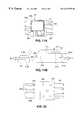
- FIG. 1is a flowchart of a conventional method of assembling an integrated circuit package having a conductive strap.
- FIG. 2is a top view of conductive epoxy dispensed on a leadframe pad.
- FIGS. 3A and 3Bare top and side views of a die attached to the leadframe pad.
- FIGS. 4A and 4Bare top and side views, respectively, of solder paste dispensed on a top face of the die.
- FIGS. 5A and 5Bare top and side views of a copper strap on the input leadfingers of the leadframe and the die.
- FIG. 6is a flowchart of a method in accordance with the present invention of assembling integrated circuit package having a conductive strap.
- FIG. 7is a top view of a conductive adhesive applied on a leadframe pad.
- FIG. 8is a top view of a conductive adhesive applied on a portion of a leadframe to which a conductive strap will be attached.
- FIGS. 9A and 9Bare top and side views of a die on the leadframe pad.
- FIGS. 10A and 10Bare top and side views of a conductive adhesive applied on a top surface of the die and the leadframe.
- FIGS. 11A and 11Bare top and side views of a conductive strap attached to the leadframe and the die.
- FIG. 12is a top view of a leadframe having unconnected input leadfingers.
- FIG. 13is a top view of a conductive strap attached to individual input leadfingers and the die.
- FIG. 14is a partially broken perspective view of an exemplary integrated circuit package assembled using the method of FIG. 6 .
- FIG. 6is a flowchart of an exemplary method within the present invention of assembling an integrated circuit package.
- FIGS. 7, 8 , 9 A, 9 B, 10 A, 10 B, 11 A and 11 Bprovide views at various stages of the process.
- Step 100a metal leadframe strip comprising an array of metal leadframes is provided. Tooling or indexing holes are located along the leadframe strip edges to mate with transfer mechanism elements and alignment pins of the assembly equipment. For ease of explanation, only one leadframe is described below.
- leadframe 202is made of a conventional leadframe metal, such as, but not limited to, copper, copper alloys, and Alloy 42 , among others.
- the leadframe 202may be plated with a variety of conventional plating metals.
- Leadframe 202includes a leadframe pad 204 and a plurality of leadfingers (e.g., input leadfingers 206 and output leadfingers 207 ).
- Leadframe pad 204provides a die mounting site while leadfingers 206 and 207 provide for electrical connections between the circuitry on an integrated circuit die 210 (FIG. 9A) and an external printed circuit board or other device (not shown).
- Input leadfingers 206 aare integrally connected at their inner ends by a conductive member 206 c that is adjacent to leadframe pad 204 .
- input leadfingers 206 aare source leads; input leadfinger 206 b is a gate lead; and output leadfingers 207 are drain leads of the package.
- Step 102 of FIG. 6loads the leadframe strip into a conventional die attach machine.
- a conventional die attach machineAs an example, an ALPHASEM SL9003 or a SL8003 die attach machine may be used. Steps 102 - 112 of FIG. 6 (i.e., up through the curing step) are performed in a single pass through the die attach machine.
- Step 104 of FIG. 6a conductive adhesive 208 is applied by the die attach machine onto leadframe pad 204 .
- a conductive adhesive 208is applied by the die attach machine onto leadframe pad 204 .
- five dots of adhesive 208are applied to leadframe pad 204 , but other arrangements of adhesive 208 also may be used.
- An alternative Step 104 shown in FIG. 8applies adhesive 208 to leadframe pad 204 and also applies adhesive 209 to leadframe member 206 c.
- Step 106 of FIG. 6picks a die 210 from a wafer tape (not shown) and places the die 210 on adhesive 208 on leadframe pad 204 .
- FIG. 9 A and FIG. 9Bshow top and side views of die 210 on adhesive 208 on leadframe pad 204 .
- Die 210has a lower first surface 210 a on adhesive 208 , and an opposite upper second surface 210 b .
- first surface 210 a an second surface 210 b of die 210are typically coated with a conductive material, such as aluminum or some other metal.
- Step 108 of FIG. 6applies conductive adhesive 212 onto second surface 210 b of die 210 .
- Step 108also applies conductive adhesive 209 to leadframe member 206 c , unless conductive adhesive 209 already was applied in Step 104 .
- FIGS. 10A and 10Bshow top and side views, respectively, after conductive adhesive 212 has been applied to second surface 210 b of die 210 and after conductive adhesive 209 has been applied to member 206 c.
- Step 110 of FIG. 6singulates a conductive strap 214 from a reel or a matrix reel and then picks and places a right-most end of conductive strap 214 onto adhesive 212 on second surface 210 b of die 210 and a left-most end of strap 214 onto adhesive 209 on leadframe member 206 c .
- FIGS. 11A and 11Bshow top and side views of a conductive strap 214 having a planar first surface 214 a on die 210 , and a planar second surface 214 b on leadframe member 206 c.
- Conductive strap 214needs to be conductive to provide electrical connection between die 210 and leadfingers 206 a .
- conductive strap 214is made of copper (Cu).
- Other conductive materialssuch as copper alloys, aluminum (Al) and aluminum alloys may also be used for strap 214 .
- the size of conductive strap 214depends on the size of die 210 and the application of the integrated circuit device. In a power MOSFET application, for example, conductive strap 214 may cover up to approximately 70% of second surface 210 b of die 210 .
- An exemplary strap 214is approximately 2667 microns by approximately 2641 microns. In general, a clearance of approximately 254 microns from the edge of die 210 should be maintained.
- Step 110is repeated until a conductive strap 214 is placed onto each die 210 and leadframe 202 of the leadframe strip through conductive adhesives 212 and 209 , respectively.
- Step 112 of FIG. 6loads the leadframe strip into a transport magazine and unloads the die attach machine.
- Step 114 of FIG. 6places the magazine of leadframe strips into a conventional convection curing oven (not shown). Subsequently, Step 114 simultaneously cures conductive adhesives 208 , 209 , and 212 .
- conductive adhesive 208is cured so that first surface 210 a of die 210 is permanently attached thereby to leadframe pad 204
- conductive adhesives 209 and 212are cured so that conductive strap 214 is permanently attached thereby to leadframe member 206 c and second surface 210 b of die 210 , respectively.
- Step 116ends the process of FIG. 6 .
- FIG. 14is a partially broken perspective view of an embodiment of an integrated circuit package 216 assembled using the method of FIG. 6 .
- package 216is a power MOSFET package. Assembly steps subsequent to the method of FIG. 6 include encapsulation of die 210 , strap 214 , wirebond 218 and the inner ends of leadfingers 206 and 207 in an insulative and protective encapsulant material 220 .
- the packageis encapsulated using conventional transfer molding techniques and materials. Examples of molding compounds include EME7200 from the Sumitomo Company and KE300 from the Toshiba Company. It is noted that the properties of the molding compound should be selected to optimize thermal, mechanical and moisture resistance of the device. The location of much of strap 214 proximate to the upper surface of package 216 allows enhanced heat dissipation.
- adhesives 208 , 209 , and 212are conductive materials that simultaneously harden upon curing and thereby permanently attach die 210 to leadframe pad 202 and conductive strap 214 to die 210 and leadframe 202 .
- Adhesives 208 , 209 and 212may be the same type of material. Alternatively, one or all of adhesive materials 208 , 209 , and 212 may differ from each other, although in such cases the materials selected should cure simultaneously in Step 114 of FIG. 6 . None of adhesives 208 , 209 , or 212 is solder. Solder paste 60 of FIGS. 4A and 4B is eliminated.
- Adhesives 208 , 209 , and 212may be any conventional conductive curable die attach adhesive such as a silver-filled conductive epoxy or other organic-based adhesives.
- epoxiessuch as 84- 1 LMISR4, LMIT1 or 8361 epoxies from the ABLESTIK Company, or A 3 from the BELLHITEC Company are some examples of adhesives 208 , 209 and 212 . It is noted that the adhesive materials should be selected such that die 210 is not subject to excessive strain during the curing step.
- the amount of material applied as adhesives 208 , 209 , and 212 in Steps 104 and 108is controlled so that the bond line thickness between die 210 and leadframe pad 204 (shown as BLT1 ), the bond line thickness between strap 214 and die 210 (shown as BLT2 ), and the bond line thickness between strap 214 and leadframe member 206 c (shown as BLT3 ) are within ranges specified for the particular packaging application.
- a typical bond line thickness rangeis 2.54 microns to 25.4 microns.
- the bond line thicknessaffects the electrical performance of the package and is generally controlled by the amount of adhesive applied and the z-travel (i.e., height travel) of the bond arm of the die attach machine.
- a bond line thickness of approximately 12.7 micronsis obtained between die 210 and leadframe pad 204 (BLT1) and between strap 214 and die 210 and leadframe member 206 c (BLT2 and BLT3, respectively).
- the curing conditions used in Step 114 of FIG. 6depend on the materials and amounts of conductive adhesives 208 , 209 , and 212 used.
- typical curing conditions for ABLESTIK 84-1LMISR4 epoxyinclude heating to a temperature in the range of approximately 170° C. to 180° C. for a time of about 60 minutes. Conventional convection curing ovens are used.
- the process of FIG. 6has the advantage of not exposing devices to high temperature reflow ovens associated with solder paste curing because solder paste is eliminated from the packaging process.
- the die attach and conductive strap attach processesare more efficient because they are performed in a single pass through the die attach machine.
- bond line thicknessmay be controlled more consistently because the same or similar adhesive materials are used for the die attach and the conductive strap attach steps and only a single adhesive curing step is used.
- the overall equipment utilizationis improved due to the removal of solder reflow process and associated cleaning processes.
- leadframe 202includes a plurality of input leadfingers 206 a connected by member 206 c .
- Conductive adhesive 209is applied onto leadframe member 206 c .
- input leadfingers 206 aneed not be connected by a conductive member, as shown in FIG. 12 .
- at least one drop of conductive adhesive 209is applied onto an inner end portion of individual leadfingers 206 a .
- Conductive strap 214is then placed onto the adhesive 209 on leadfingers 206 a and on die 210 so that, after curing, conductive strap 214 is physically and electrically connected between leadfingers 206 a and die 210 , as shown in FIG. 13 .
- Other process steps for this alternative embodimentare similar to those described above in conjunction with FIG. 6 .
Landscapes
- Engineering & Computer Science (AREA)
- Computer Hardware Design (AREA)
- Microelectronics & Electronic Packaging (AREA)
- Power Engineering (AREA)
- Physics & Mathematics (AREA)
- Condensed Matter Physics & Semiconductors (AREA)
- General Physics & Mathematics (AREA)
- Die Bonding (AREA)
Abstract
Description
Claims (20)
Priority Applications (2)
| Application Number | Priority Date | Filing Date | Title |
|---|---|---|---|
| US09/452,545US6319755B1 (en) | 1999-12-01 | 1999-12-01 | Conductive strap attachment process that allows electrical connector between an integrated circuit die and leadframe |
| US10/256,905US6707138B2 (en) | 1999-12-01 | 2002-09-26 | Semiconductor device including metal strap electrically coupled between semiconductor die and metal leadframe |
Applications Claiming Priority (1)
| Application Number | Priority Date | Filing Date | Title |
|---|---|---|---|
| US09/452,545US6319755B1 (en) | 1999-12-01 | 1999-12-01 | Conductive strap attachment process that allows electrical connector between an integrated circuit die and leadframe |
Related Child Applications (1)
| Application Number | Title | Priority Date | Filing Date |
|---|---|---|---|
| US10/256,905ContinuationUS6707138B2 (en) | 1999-12-01 | 2002-09-26 | Semiconductor device including metal strap electrically coupled between semiconductor die and metal leadframe |
Publications (1)
| Publication Number | Publication Date |
|---|---|
| US6319755B1true US6319755B1 (en) | 2001-11-20 |
Family
ID=23796897
Family Applications (1)
| Application Number | Title | Priority Date | Filing Date |
|---|---|---|---|
| US09/452,545Expired - LifetimeUS6319755B1 (en) | 1999-12-01 | 1999-12-01 | Conductive strap attachment process that allows electrical connector between an integrated circuit die and leadframe |
Country Status (1)
| Country | Link |
|---|---|
| US (1) | US6319755B1 (en) |
Cited By (34)
| Publication number | Priority date | Publication date | Assignee | Title |
|---|---|---|---|---|
| US6465276B2 (en)* | 2000-05-18 | 2002-10-15 | Siliconx (Taiwan) Ltd. | Power semiconductor package and method for making the same |
| US6589859B2 (en)* | 2000-07-07 | 2003-07-08 | Alstom | Method of manufacturing an electronic power component, and an electronic power component obtained thereby |
| US6707138B2 (en)* | 1999-12-01 | 2004-03-16 | Amkor Technology, Inc. | Semiconductor device including metal strap electrically coupled between semiconductor die and metal leadframe |
| US6723582B2 (en)* | 2000-12-07 | 2004-04-20 | Amkor Technology, Inc. | Method of making a semiconductor package having exposed metal strap |
| DE10249206B3 (en)* | 2002-10-22 | 2004-07-01 | Siemens Ag | Method of assembling a power device |
| US20050017339A1 (en)* | 2003-06-19 | 2005-01-27 | Shigeharu Yoshiba | Semiconductor device and switching element |
| US6849930B2 (en)* | 2000-08-31 | 2005-02-01 | Nec Corporation | Semiconductor device with uneven metal plate to improve adhesion to molding compound |
| US20050130350A1 (en)* | 2000-04-13 | 2005-06-16 | Estacio Maria Cristina B. | Flip clip attach and copper clip attach on MOSFET device |
| US20050167848A1 (en)* | 1999-12-16 | 2005-08-04 | Fairchild Semiconductor Corporation | Filp chip in leaded molded package and method of manufacture thereof |
| US20050212101A1 (en)* | 2001-04-18 | 2005-09-29 | Norihide Funato | Semiconductor device and method of manufacturing the same |
| US20060055011A1 (en)* | 2004-09-16 | 2006-03-16 | Semiconductor Components Industries, Llc | Robust power semiconductor package |
| US20060237814A1 (en)* | 2005-03-09 | 2006-10-26 | Khalil Hosseini | Semiconductor device having surface mountable external contact areas and method for producing the same |
| US20070040252A1 (en)* | 2005-08-17 | 2007-02-22 | Khalil Hosseini | Semiconductor power component with a vertical current path through a semiconductor power chip |
| US20070231953A1 (en)* | 2006-03-31 | 2007-10-04 | Yoshihiro Tomita | Flexible interconnect pattern on semiconductor package |
| US20070228556A1 (en)* | 2006-03-31 | 2007-10-04 | Infineon Technologies Ag | Power Semiconductor Component with a Power Semiconductor Chip and Method for Producing the Same |
| US20070241328A1 (en)* | 2006-04-12 | 2007-10-18 | Infineon Technologies Ag | Process for producing power semiconductor components using a marker |
| DE102006017101A1 (en)* | 2006-04-10 | 2007-10-18 | Phoenix Contact Gmbh & Co. Kg | Rigid-flexible printed circuit board for electrical device, has sliding bow fastened to contact of multi-contact components e.g. unpackaged power semiconductor, with conductive adhesive that is applied by dosing machine |
| US20080036078A1 (en)* | 2006-08-14 | 2008-02-14 | Ciclon Semiconductor Device Corp. | Wirebond-less semiconductor package |
| US20080044946A1 (en)* | 2005-11-18 | 2008-02-21 | Cruz Erwin Victor R | Semiconductor die package using leadframe and clip and method of manufacturing |
| US20080146010A1 (en)* | 2006-12-19 | 2008-06-19 | Khalil Hosseini | Semiconductor component comprising a semiconductor chip and method for producing the same |
| US20080150105A1 (en)* | 2005-06-13 | 2008-06-26 | Infineon Technologies Ag | Power Semiconductor Component Stack Using Lead Technology with Surface-Mountable External Contacts and a Method for Producing the Same |
| US20080246165A1 (en)* | 2007-04-04 | 2008-10-09 | Freescale Semiconductor, Inc. | Novel interconnect for chip level power distribution |
| US20090057854A1 (en)* | 2007-08-28 | 2009-03-05 | Gomez Jocel P | Self locking and aligning clip structure for semiconductor die package |
| US20090294934A1 (en)* | 2008-05-30 | 2009-12-03 | Alpha & Omega Semiconductor, Ltd. | Conductive clip for semiconductor device package |
| US20100164078A1 (en)* | 2008-12-31 | 2010-07-01 | Ruben Madrid | Package assembly for semiconductor devices |
| US20100270663A1 (en)* | 2007-05-10 | 2010-10-28 | Freescale Semiconductor, Inc. | Power Lead-on-Chip Ball Grid Array Package |
| CN103633050A (en)* | 2013-11-29 | 2014-03-12 | 华为技术有限公司 | Chip, chip packaging structure and chip welding method |
| US8791582B2 (en) | 2010-07-28 | 2014-07-29 | Freescale Semiconductor, Inc. | Integrated circuit package with voltage distributor |
| US9196598B1 (en) | 2014-06-12 | 2015-11-24 | Freescale Semiconductor, Inc. | Semiconductor device having power distribution using bond wires |
| CN108364942A (en)* | 2017-01-27 | 2018-08-03 | 瑞萨电子株式会社 | Semiconductor devices |
| CN112289779A (en)* | 2019-07-25 | 2021-01-29 | 恩智浦有限公司 | Semiconductor device and method |
| US20210062047A1 (en)* | 2018-05-16 | 2021-03-04 | Henkel Ag & Co. Kgaa | Curable adhesive composition for die attach |
| EP3813106A1 (en)* | 2019-10-21 | 2021-04-28 | Renesas Electronics Corporation | Semiconductor device |
| US11183450B2 (en)* | 2018-03-26 | 2021-11-23 | Texas Instruments Incorporated | Electronic device having inverted lead pins |
Citations (11)
| Publication number | Priority date | Publication date | Assignee | Title |
|---|---|---|---|---|
| US4189342A (en) | 1971-10-07 | 1980-02-19 | U.S. Philips Corporation | Semiconductor device comprising projecting contact layers |
| JPS60116239A (en) | 1983-11-28 | 1985-06-22 | Nec Corp | Radio communication equipment |
| US4935803A (en) | 1988-09-09 | 1990-06-19 | Motorola, Inc. | Self-centering electrode for power devices |
| US5218231A (en) | 1989-08-30 | 1993-06-08 | Kabushiki Kaisha Toshiba | Mold-type semiconductor device |
| US5266834A (en) | 1989-03-13 | 1993-11-30 | Hitachi Ltd. | Semiconductor device and an electronic device with the semiconductor devices mounted thereon |
| JPH0864634A (en) | 1994-08-23 | 1996-03-08 | Hitachi Ltd | Semiconductor device and manufacturing method thereof |
| EP0720225A2 (en) | 1994-12-30 | 1996-07-03 | SILICONIX Incorporated | Lateral power MOSFET having metal strap layer to reduce distributed resistance and method of fabricating the same |
| EP0720234A2 (en) | 1994-12-30 | 1996-07-03 | SILICONIX Incorporated | Vertical power MOSFET having thick metal layer to reduce distributed resistance and method of fabricating the same |
| US5544412A (en) | 1994-05-24 | 1996-08-13 | Motorola, Inc. | Method for coupling a power lead to a bond pad in an electronic module |
| US5814884A (en)* | 1996-10-24 | 1998-09-29 | International Rectifier Corporation | Commonly housed diverse semiconductor die |
| US6040626A (en)* | 1998-09-25 | 2000-03-21 | International Rectifier Corp. | Semiconductor package |
- 1999
- 1999-12-01USUS09/452,545patent/US6319755B1/ennot_activeExpired - Lifetime
Patent Citations (13)
| Publication number | Priority date | Publication date | Assignee | Title |
|---|---|---|---|---|
| US4189342A (en) | 1971-10-07 | 1980-02-19 | U.S. Philips Corporation | Semiconductor device comprising projecting contact layers |
| JPS60116239A (en) | 1983-11-28 | 1985-06-22 | Nec Corp | Radio communication equipment |
| US4935803A (en) | 1988-09-09 | 1990-06-19 | Motorola, Inc. | Self-centering electrode for power devices |
| US5266834A (en) | 1989-03-13 | 1993-11-30 | Hitachi Ltd. | Semiconductor device and an electronic device with the semiconductor devices mounted thereon |
| US5218231A (en) | 1989-08-30 | 1993-06-08 | Kabushiki Kaisha Toshiba | Mold-type semiconductor device |
| US5544412A (en) | 1994-05-24 | 1996-08-13 | Motorola, Inc. | Method for coupling a power lead to a bond pad in an electronic module |
| JPH0864634A (en) | 1994-08-23 | 1996-03-08 | Hitachi Ltd | Semiconductor device and manufacturing method thereof |
| EP0720225A2 (en) | 1994-12-30 | 1996-07-03 | SILICONIX Incorporated | Lateral power MOSFET having metal strap layer to reduce distributed resistance and method of fabricating the same |
| EP0720234A2 (en) | 1994-12-30 | 1996-07-03 | SILICONIX Incorporated | Vertical power MOSFET having thick metal layer to reduce distributed resistance and method of fabricating the same |
| US5665996A (en) | 1994-12-30 | 1997-09-09 | Siliconix Incorporated | Vertical power mosfet having thick metal layer to reduce distributed resistance |
| US5814884A (en)* | 1996-10-24 | 1998-09-29 | International Rectifier Corporation | Commonly housed diverse semiconductor die |
| US5814884C1 (en)* | 1996-10-24 | 2002-01-29 | Int Rectifier Corp | Commonly housed diverse semiconductor die |
| US6040626A (en)* | 1998-09-25 | 2000-03-21 | International Rectifier Corp. | Semiconductor package |
Non-Patent Citations (3)
| Title |
|---|
| http://www.siliconix.com, "New Package Technology Yields Nearly Twofold Improvement Over Previous State-of-the-art," Vishay Siliconix Press Release, Dec. 9, 1998. |
| Mannion, P., "MOSFETs Break Out Of The Shackles Of Wirebonding", Electronic Design, vol. 47, No. 6 (Mar. 22, 1999). |
| Provisional U.S. Patent application No. 60/101,810, filed Sep. 25, 1998, published Mar. 21, 2000 upon issuance of U.S. Patent No. 6,040,626. |
Cited By (72)
| Publication number | Priority date | Publication date | Assignee | Title |
|---|---|---|---|---|
| US6707138B2 (en)* | 1999-12-01 | 2004-03-16 | Amkor Technology, Inc. | Semiconductor device including metal strap electrically coupled between semiconductor die and metal leadframe |
| US7215011B2 (en) | 1999-12-16 | 2007-05-08 | Fairchild Semiconductor Corporation | Flip chip in leaded molded package and method of manufacture thereof |
| US7154168B2 (en)* | 1999-12-16 | 2006-12-26 | Fairchild Semiconductor Corporation | Flip chip in leaded molded package and method of manufacture thereof |
| US20080036056A1 (en)* | 1999-12-16 | 2008-02-14 | Rajeev Joshi | Flip chip in leaded molded package and method of manufacture thereof |
| US7582956B2 (en) | 1999-12-16 | 2009-09-01 | Fairchild Semiconductor Corporation | Flip chip in leaded molded package and method of manufacture thereof |
| US20050167848A1 (en)* | 1999-12-16 | 2005-08-04 | Fairchild Semiconductor Corporation | Filp chip in leaded molded package and method of manufacture thereof |
| US20050280126A1 (en)* | 1999-12-16 | 2005-12-22 | Rajeev Joshi | Flip chip in leaded molded package and method of manufacture thereof |
| US7052938B2 (en) | 2000-04-13 | 2006-05-30 | Fairchild Semiconductor Corporation | Flip clip attach and copper clip attach on MOSFET device |
| US20050130350A1 (en)* | 2000-04-13 | 2005-06-16 | Estacio Maria Cristina B. | Flip clip attach and copper clip attach on MOSFET device |
| US6465276B2 (en)* | 2000-05-18 | 2002-10-15 | Siliconx (Taiwan) Ltd. | Power semiconductor package and method for making the same |
| US6589859B2 (en)* | 2000-07-07 | 2003-07-08 | Alstom | Method of manufacturing an electronic power component, and an electronic power component obtained thereby |
| US6849930B2 (en)* | 2000-08-31 | 2005-02-01 | Nec Corporation | Semiconductor device with uneven metal plate to improve adhesion to molding compound |
| US6723582B2 (en)* | 2000-12-07 | 2004-04-20 | Amkor Technology, Inc. | Method of making a semiconductor package having exposed metal strap |
| US20070052075A1 (en)* | 2001-04-18 | 2007-03-08 | Norihide Funato | Semiconductor device and method of manufacturing the same |
| US7364950B2 (en) | 2001-04-18 | 2008-04-29 | Kabushiki Kaisha Toshiba | Semiconductor device and method of manufacturing the same |
| US20050212101A1 (en)* | 2001-04-18 | 2005-09-29 | Norihide Funato | Semiconductor device and method of manufacturing the same |
| US7230322B2 (en)* | 2001-04-18 | 2007-06-12 | Kabushiki Kaisha Toshiba | Semiconductor device and method of manufacturing the same |
| DE10249206B3 (en)* | 2002-10-22 | 2004-07-01 | Siemens Ag | Method of assembling a power device |
| US20050017339A1 (en)* | 2003-06-19 | 2005-01-27 | Shigeharu Yoshiba | Semiconductor device and switching element |
| US7030501B2 (en)* | 2003-06-19 | 2006-04-18 | Sanyo Electric Co., Ltd. | Semiconductor device and switching element |
| US20060055011A1 (en)* | 2004-09-16 | 2006-03-16 | Semiconductor Components Industries, Llc | Robust power semiconductor package |
| US7135761B2 (en)* | 2004-09-16 | 2006-11-14 | Semiconductor Components Industries, L.Lc | Robust power semiconductor package |
| DE102005011159B4 (en)* | 2005-03-09 | 2013-05-16 | Infineon Technologies Ag | Semiconductor device having surface mount external contact pads and method of making the same |
| US20060237814A1 (en)* | 2005-03-09 | 2006-10-26 | Khalil Hosseini | Semiconductor device having surface mountable external contact areas and method for producing the same |
| US7579675B2 (en) | 2005-03-09 | 2009-08-25 | Infineon Technologies Ag | Semiconductor device having surface mountable external contact areas and method for producing the same |
| US7728415B2 (en) | 2005-06-13 | 2010-06-01 | Infineon Technologies Ag | Power semiconductor component stack using lead technology with surface-mountable external contacts and a method for producing the same |
| US20080150105A1 (en)* | 2005-06-13 | 2008-06-26 | Infineon Technologies Ag | Power Semiconductor Component Stack Using Lead Technology with Surface-Mountable External Contacts and a Method for Producing the Same |
| US7632718B2 (en)* | 2005-08-17 | 2009-12-15 | Infineon Technologies Ag | Semiconductor power component with a vertical current path through a semiconductor power chip |
| US20070040252A1 (en)* | 2005-08-17 | 2007-02-22 | Khalil Hosseini | Semiconductor power component with a vertical current path through a semiconductor power chip |
| US8058107B2 (en) | 2005-11-18 | 2011-11-15 | Cruz Erwin Victor R | Semiconductor die package using leadframe and clip and method of manufacturing |
| US20080044946A1 (en)* | 2005-11-18 | 2008-02-21 | Cruz Erwin Victor R | Semiconductor die package using leadframe and clip and method of manufacturing |
| US8409924B2 (en) | 2006-03-31 | 2013-04-02 | Intel Corporation | Flexible interconnect pattern on semiconductor package |
| US7915081B2 (en)* | 2006-03-31 | 2011-03-29 | Intel Corporation | Flexible interconnect pattern on semiconductor package |
| US20110103438A1 (en)* | 2006-03-31 | 2011-05-05 | Intel Corporation | Flexible interconnect pattern on semiconductor package |
| US8518750B2 (en) | 2006-03-31 | 2013-08-27 | Intel Corporation | Flexible interconnect pattern on semiconductor package |
| US8227907B2 (en)* | 2006-03-31 | 2012-07-24 | Intel Corporation | Flexible interconnect pattern on semiconductor package |
| US20070228556A1 (en)* | 2006-03-31 | 2007-10-04 | Infineon Technologies Ag | Power Semiconductor Component with a Power Semiconductor Chip and Method for Producing the Same |
| US20070231953A1 (en)* | 2006-03-31 | 2007-10-04 | Yoshihiro Tomita | Flexible interconnect pattern on semiconductor package |
| US7745913B2 (en) | 2006-03-31 | 2010-06-29 | Infineon Technologies Ag | Power semiconductor component with a power semiconductor chip and method for producing the same |
| DE102006017101A1 (en)* | 2006-04-10 | 2007-10-18 | Phoenix Contact Gmbh & Co. Kg | Rigid-flexible printed circuit board for electrical device, has sliding bow fastened to contact of multi-contact components e.g. unpackaged power semiconductor, with conductive adhesive that is applied by dosing machine |
| DE102006017101B4 (en)* | 2006-04-10 | 2014-03-20 | Phoenix Contact Gmbh & Co. Kg | Printed circuit board and electrical device |
| US20070241328A1 (en)* | 2006-04-12 | 2007-10-18 | Infineon Technologies Ag | Process for producing power semiconductor components using a marker |
| US20080036078A1 (en)* | 2006-08-14 | 2008-02-14 | Ciclon Semiconductor Device Corp. | Wirebond-less semiconductor package |
| US8304903B2 (en)* | 2006-08-14 | 2012-11-06 | Texas Instruments Incorporated | Wirebond-less semiconductor package |
| US20110095411A1 (en)* | 2006-08-14 | 2011-04-28 | Texas Instruments Incorporated | Wirebond-less Semiconductor Package |
| US7851927B2 (en) | 2006-12-19 | 2010-12-14 | Infineon Technologies Ag | Semiconductor component comprising a semiconductor chip and semiconductor component carrier with external connection strips |
| US20080146010A1 (en)* | 2006-12-19 | 2008-06-19 | Khalil Hosseini | Semiconductor component comprising a semiconductor chip and method for producing the same |
| US7829997B2 (en)* | 2007-04-04 | 2010-11-09 | Freescale Semiconductor, Inc. | Interconnect for chip level power distribution |
| US20080246165A1 (en)* | 2007-04-04 | 2008-10-09 | Freescale Semiconductor, Inc. | Novel interconnect for chip level power distribution |
| US20100270663A1 (en)* | 2007-05-10 | 2010-10-28 | Freescale Semiconductor, Inc. | Power Lead-on-Chip Ball Grid Array Package |
| US8129226B2 (en) | 2007-05-10 | 2012-03-06 | Freescale Semiconductor, Inc. | Power lead-on-chip ball grid array package |
| US8067273B2 (en) | 2007-08-28 | 2011-11-29 | Fairchild Semiconductor Corporation | Self locking and aligning clip structure for semiconductor die package |
| US20110076807A1 (en)* | 2007-08-28 | 2011-03-31 | Gomez Jocel P | Self locking and aligning clip structure for semiconductor die package |
| US7902657B2 (en)* | 2007-08-28 | 2011-03-08 | Fairchild Semiconductor Corporation | Self locking and aligning clip structure for semiconductor die package |
| US20090057854A1 (en)* | 2007-08-28 | 2009-03-05 | Gomez Jocel P | Self locking and aligning clip structure for semiconductor die package |
| US20090294934A1 (en)* | 2008-05-30 | 2009-12-03 | Alpha & Omega Semiconductor, Ltd. | Conductive clip for semiconductor device package |
| US8680658B2 (en)* | 2008-05-30 | 2014-03-25 | Alpha And Omega Semiconductor Incorporated | Conductive clip for semiconductor device package |
| US20100164078A1 (en)* | 2008-12-31 | 2010-07-01 | Ruben Madrid | Package assembly for semiconductor devices |
| US8791582B2 (en) | 2010-07-28 | 2014-07-29 | Freescale Semiconductor, Inc. | Integrated circuit package with voltage distributor |
| US9331046B2 (en) | 2010-07-28 | 2016-05-03 | Freescale Semiconductor, Inc. | Integrated circuit package with voltage distributor |
| CN103633050A (en)* | 2013-11-29 | 2014-03-12 | 华为技术有限公司 | Chip, chip packaging structure and chip welding method |
| US9196598B1 (en) | 2014-06-12 | 2015-11-24 | Freescale Semiconductor, Inc. | Semiconductor device having power distribution using bond wires |
| CN108364942A (en)* | 2017-01-27 | 2018-08-03 | 瑞萨电子株式会社 | Semiconductor devices |
| US11183450B2 (en)* | 2018-03-26 | 2021-11-23 | Texas Instruments Incorporated | Electronic device having inverted lead pins |
| US20220068790A1 (en)* | 2018-03-26 | 2022-03-03 | Texas Instruments Incorporated | Electronic Device Having Inverted Lead Pins |
| US11699649B2 (en)* | 2018-03-26 | 2023-07-11 | Texas Instruments Incorporated | Electronic device having inverted lead pins |
| US20210062047A1 (en)* | 2018-05-16 | 2021-03-04 | Henkel Ag & Co. Kgaa | Curable adhesive composition for die attach |
| CN112289779A (en)* | 2019-07-25 | 2021-01-29 | 恩智浦有限公司 | Semiconductor device and method |
| CN112289779B (en)* | 2019-07-25 | 2025-06-17 | 恩智浦有限公司 | Semiconductor device and method |
| EP3813106A1 (en)* | 2019-10-21 | 2021-04-28 | Renesas Electronics Corporation | Semiconductor device |
| JP2021068783A (en)* | 2019-10-21 | 2021-04-30 | ルネサスエレクトロニクス株式会社 | Semiconductor device |
| US11444010B2 (en) | 2019-10-21 | 2022-09-13 | Renesas Electronics Corporation | Semiconductor device |
Similar Documents
| Publication | Publication Date | Title |
|---|---|---|
| US6319755B1 (en) | Conductive strap attachment process that allows electrical connector between an integrated circuit die and leadframe | |
| US7834433B2 (en) | Semiconductor power device | |
| US6501183B2 (en) | Semiconductor device and a method of manufacturing the same and an electronic device | |
| US6781243B1 (en) | Leadless leadframe package substitute and stack package | |
| US6458625B2 (en) | Multi chip semiconductor package and method of construction | |
| US6878570B2 (en) | Thin stacked package and manufacturing method thereof | |
| US7737537B2 (en) | Electronic device | |
| US8513059B2 (en) | Pre-molded clip structure | |
| CN102420217B (en) | Multi-chip semiconductor packages and assembling thereof | |
| JP2582013B2 (en) | Resin-sealed semiconductor device and method of manufacturing the same | |
| US8354303B2 (en) | Thermally enhanced low parasitic power semiconductor package | |
| US20110244633A1 (en) | Package assembly for semiconductor devices | |
| US20100193922A1 (en) | Semiconductor chip package | |
| US5822848A (en) | Lead frame having a detachable and interchangeable die-attach paddle | |
| US20090127676A1 (en) | Back to Back Die Assembly For Semiconductor Devices | |
| KR20070034438A (en) | Method of making a stacked die package | |
| JPH02285646A (en) | Resin sealed semiconductor device and formation thereof | |
| US5299091A (en) | Packaged semiconductor device having heat dissipation/electrical connection bumps and method of manufacturing same | |
| US6677665B2 (en) | Dual-die integrated circuit package | |
| US7728411B2 (en) | COL-TSOP with nonconductive material for reducing package capacitance | |
| US20060091516A1 (en) | Flexible leaded stacked semiconductor package | |
| US8097952B2 (en) | Electronic package structure having conductive strip and method | |
| EP3761360B1 (en) | Power die package | |
| JP3125891B2 (en) | Semiconductor device | |
| US20250079261A1 (en) | Semiconductor packages with thermal dissipation |
Legal Events
| Date | Code | Title | Description |
|---|---|---|---|
| AS | Assignment | Owner name:AMKOR TECHNOLOGY, INC., ARIZONA Free format text:ASSIGNMENT OF ASSIGNORS INTEREST;ASSIGNOR:MAURI, PHILIP S.;REEL/FRAME:010868/0486 Effective date:19991201 | |
| STCF | Information on status: patent grant | Free format text:PATENTED CASE | |
| CC | Certificate of correction | ||
| AS | Assignment | Owner name:CITICORP USA, INC. AS "COLLATERAL AGENT", DELAWARE Free format text:SECURITY INTEREST;ASSIGNORS:AMKOR TECHNOLOGY, INC.;GUARDIAN ASSETS, INC.;REEL/FRAME:013974/0893 Effective date:20030422 | |
| AS | Assignment | Owner name:CITICORP NORTH AMERICA, INC. AS ADMINISTRATIVE AGE Free format text:SECURITY AGREEMENT;ASSIGNORS:AMKOR TECHNOLOGY, INC.;GUARDIAN ASSETS, INC.;REEL/FRAME:014885/0691 Effective date:20040629 | |
| AS | Assignment | Owner name:AMKOR TECHNOLOGY, INC., PENNSYLVANIA Free format text:RELEASE OF LIEN ON PATENTS;ASSIGNOR:CITICORP USA, INC. AS COLLATERAL AGENT;REEL/FRAME:015603/0572 Effective date:20040629 | |
| AS | Assignment | Owner name:CITICORP NORTH AMERICA, INC. AS "AGENT", NEW YORK Free format text:SECURITY AGREEMENT;ASSIGNORS:AMKOR TECHNOLOGY, INC.;GUARDIAN ASSETS, INC.;REEL/FRAME:015942/0521 Effective date:20041027 | |
| FEPP | Fee payment procedure | Free format text:PAYOR NUMBER ASSIGNED (ORIGINAL EVENT CODE: ASPN); ENTITY STATUS OF PATENT OWNER: LARGE ENTITY | |
| FPAY | Fee payment | Year of fee payment:4 | |
| AS | Assignment | Owner name:AMKOR TECHNOLOGY, INC., ARIZONA Free format text:TERMINATION & RELEASE OF PATENT SECURITY AGREEMENT;ASSIGNOR:CITICORP NORTH AMERICA, INC.;REEL/FRAME:017388/0868 Effective date:20051128 Owner name:BANK OF AMERICA, N.A., TEXAS Free format text:SECURITY AGREEMENT;ASSIGNOR:AMKOR TECHNOLOGY, INC.;REEL/FRAME:017379/0630 Effective date:20051123 | |
| FPAY | Fee payment | Year of fee payment:8 | |
| FPAY | Fee payment | Year of fee payment:12 | |
| AS | Assignment | Owner name:BANK OF AMERICA, N.A., AS AGENT, CALIFORNIA Free format text:SECURITY INTEREST;ASSIGNOR:AMKOR TECHNOLOGY, INC.;REEL/FRAME:046683/0139 Effective date:20180713 | |
| AS | Assignment | Owner name:AMKOR TECHNOLOGY SINGAPORE HOLDING PTE.LTD., SINGAPORE Free format text:ASSIGNMENT OF ASSIGNORS INTEREST;ASSIGNOR:AMKOR TECHNOLOGY, INC.;REEL/FRAME:054036/0599 Effective date:20191119 |