US6317948B1 - Embedded thin film passive components - Google Patents
Embedded thin film passive componentsDownload PDFInfo
- Publication number
- US6317948B1 US6317948B1US09/291,781US29178199AUS6317948B1US 6317948 B1US6317948 B1US 6317948B1US 29178199 AUS29178199 AUS 29178199AUS 6317948 B1US6317948 B1US 6317948B1
- Authority
- US
- United States
- Prior art keywords
- layer
- circuit board
- printed circuit
- holes
- capacitor
- Prior art date
- Legal status (The legal status is an assumption and is not a legal conclusion. Google has not performed a legal analysis and makes no representation as to the accuracy of the status listed.)
- Expired - Lifetime
Links
- 239000010409thin filmSubstances0.000titledescription4
- 239000003990capacitorSubstances0.000claimsabstractdescription48
- 238000000034methodMethods0.000claimsabstractdescription27
- 238000004519manufacturing processMethods0.000claimsabstractdescription3
- 229910052751metalInorganic materials0.000claimsdescription10
- 239000002184metalSubstances0.000claimsdescription10
- 238000000151depositionMethods0.000claimsdescription9
- 239000000463materialSubstances0.000claimsdescription8
- 229910052782aluminiumInorganic materials0.000claimsdescription7
- XAGFODPZIPBFFR-UHFFFAOYSA-NaluminiumChemical compound[Al]XAGFODPZIPBFFR-UHFFFAOYSA-N0.000claimsdescription6
- 238000000059patterningMethods0.000claimsdescription6
- 230000015572biosynthetic processEffects0.000claimsdescription5
- 229910052715tantalumInorganic materials0.000claimsdescription5
- 238000007743anodisingMethods0.000claimsdescription4
- 229910021420polycrystalline siliconInorganic materials0.000claimsdescription4
- 229920005591polysiliconPolymers0.000claimsdescription4
- 238000000206photolithographyMethods0.000claimsdescription3
- RYGMFSIKBFXOCR-UHFFFAOYSA-NCopperChemical compound[Cu]RYGMFSIKBFXOCR-UHFFFAOYSA-N0.000claimsdescription2
- 229910052802copperInorganic materials0.000claimsdescription2
- 239000010949copperSubstances0.000claimsdescription2
- 229910052719titaniumInorganic materials0.000claimsdescription2
- 229910052726zirconiumInorganic materials0.000claimsdescription2
- 239000011248coating agentSubstances0.000claims2
- 238000000576coating methodMethods0.000claims2
- 239000004020conductorSubstances0.000description6
- XKRFYHLGVUSROY-UHFFFAOYSA-NArgonChemical compound[Ar]XKRFYHLGVUSROY-UHFFFAOYSA-N0.000description4
- 238000005516engineering processMethods0.000description4
- 238000004544sputter depositionMethods0.000description4
- GUVRBAGPIYLISA-UHFFFAOYSA-Ntantalum atomChemical compound[Ta]GUVRBAGPIYLISA-UHFFFAOYSA-N0.000description4
- KRKNYBCHXYNGOX-UHFFFAOYSA-Ncitric acidChemical compoundOC(=O)CC(O)(C(O)=O)CC(O)=OKRKNYBCHXYNGOX-UHFFFAOYSA-N0.000description3
- 230000008021depositionEffects0.000description3
- 239000010408filmSubstances0.000description3
- IJGRMHOSHXDMSA-UHFFFAOYSA-NAtomic nitrogenChemical compoundN#NIJGRMHOSHXDMSA-UHFFFAOYSA-N0.000description2
- 229910052786argonInorganic materials0.000description2
- BASFCYQUMIYNBI-UHFFFAOYSA-NplatinumChemical compound[Pt]BASFCYQUMIYNBI-UHFFFAOYSA-N0.000description2
- 229920001721polyimidePolymers0.000description2
- 239000004593EpoxySubstances0.000description1
- GRYLNZFGIOXLOG-UHFFFAOYSA-NNitric acidChemical compoundO[N+]([O-])=OGRYLNZFGIOXLOG-UHFFFAOYSA-N0.000description1
- 239000004642PolyimideSubstances0.000description1
- 239000000853adhesiveSubstances0.000description1
- 230000001070adhesive effectEffects0.000description1
- 239000003989dielectric materialSubstances0.000description1
- 239000002019doping agentSubstances0.000description1
- 238000005553drillingMethods0.000description1
- 239000003792electrolyteSubstances0.000description1
- 230000008020evaporationEffects0.000description1
- 238000001704evaporationMethods0.000description1
- 239000007943implantSubstances0.000description1
- 239000012212insulatorSubstances0.000description1
- 238000005304joiningMethods0.000description1
- 238000001459lithographyMethods0.000description1
- 230000000873masking effectEffects0.000description1
- 238000012986modificationMethods0.000description1
- 230000004048modificationEffects0.000description1
- 229910017604nitric acidInorganic materials0.000description1
- 150000004767nitridesChemical class0.000description1
- 229910052757nitrogenInorganic materials0.000description1
- BPUBBGLMJRNUCC-UHFFFAOYSA-Noxygen(2-);tantalum(5+)Chemical compound[O-2].[O-2].[O-2].[O-2].[O-2].[Ta+5].[Ta+5]BPUBBGLMJRNUCC-UHFFFAOYSA-N0.000description1
- 238000007747platingMethods0.000description1
- 229910052697platinumInorganic materials0.000description1
- 239000002861polymer materialSubstances0.000description1
- MZLGASXMSKOWSE-UHFFFAOYSA-Ntantalum nitrideChemical compound[Ta]#NMZLGASXMSKOWSE-UHFFFAOYSA-N0.000description1
- 229910001936tantalum oxideInorganic materials0.000description1
- XLYOFNOQVPJJNP-UHFFFAOYSA-NwaterSubstancesOXLYOFNOQVPJJNP-UHFFFAOYSA-N0.000description1
Images


Classifications
- H—ELECTRICITY
- H05—ELECTRIC TECHNIQUES NOT OTHERWISE PROVIDED FOR
- H05K—PRINTED CIRCUITS; CASINGS OR CONSTRUCTIONAL DETAILS OF ELECTRIC APPARATUS; MANUFACTURE OF ASSEMBLAGES OF ELECTRICAL COMPONENTS
- H05K1/00—Printed circuits
- H05K1/16—Printed circuits incorporating printed electric components, e.g. printed resistor, capacitor, inductor
- H05K1/162—Printed circuits incorporating printed electric components, e.g. printed resistor, capacitor, inductor incorporating printed capacitors
- H—ELECTRICITY
- H05—ELECTRIC TECHNIQUES NOT OTHERWISE PROVIDED FOR
- H05K—PRINTED CIRCUITS; CASINGS OR CONSTRUCTIONAL DETAILS OF ELECTRIC APPARATUS; MANUFACTURE OF ASSEMBLAGES OF ELECTRICAL COMPONENTS
- H05K1/00—Printed circuits
- H05K1/16—Printed circuits incorporating printed electric components, e.g. printed resistor, capacitor, inductor
- H05K1/165—Printed circuits incorporating printed electric components, e.g. printed resistor, capacitor, inductor incorporating printed inductors
- H—ELECTRICITY
- H05—ELECTRIC TECHNIQUES NOT OTHERWISE PROVIDED FOR
- H05K—PRINTED CIRCUITS; CASINGS OR CONSTRUCTIONAL DETAILS OF ELECTRIC APPARATUS; MANUFACTURE OF ASSEMBLAGES OF ELECTRICAL COMPONENTS
- H05K1/00—Printed circuits
- H05K1/16—Printed circuits incorporating printed electric components, e.g. printed resistor, capacitor, inductor
- H05K1/167—Printed circuits incorporating printed electric components, e.g. printed resistor, capacitor, inductor incorporating printed resistors
- H—ELECTRICITY
- H05—ELECTRIC TECHNIQUES NOT OTHERWISE PROVIDED FOR
- H05K—PRINTED CIRCUITS; CASINGS OR CONSTRUCTIONAL DETAILS OF ELECTRIC APPARATUS; MANUFACTURE OF ASSEMBLAGES OF ELECTRICAL COMPONENTS
- H05K2201/00—Indexing scheme relating to printed circuits covered by H05K1/00
- H05K2201/01—Dielectrics
- H05K2201/0137—Materials
- H05K2201/0175—Inorganic, non-metallic layer, e.g. resist or dielectric for printed capacitor
- H—ELECTRICITY
- H05—ELECTRIC TECHNIQUES NOT OTHERWISE PROVIDED FOR
- H05K—PRINTED CIRCUITS; CASINGS OR CONSTRUCTIONAL DETAILS OF ELECTRIC APPARATUS; MANUFACTURE OF ASSEMBLAGES OF ELECTRICAL COMPONENTS
- H05K2201/00—Indexing scheme relating to printed circuits covered by H05K1/00
- H05K2201/01—Dielectrics
- H05K2201/0137—Materials
- H05K2201/0179—Thin film deposited insulating layer, e.g. inorganic layer for printed capacitor
- H—ELECTRICITY
- H05—ELECTRIC TECHNIQUES NOT OTHERWISE PROVIDED FOR
- H05K—PRINTED CIRCUITS; CASINGS OR CONSTRUCTIONAL DETAILS OF ELECTRIC APPARATUS; MANUFACTURE OF ASSEMBLAGES OF ELECTRICAL COMPONENTS
- H05K2201/00—Indexing scheme relating to printed circuits covered by H05K1/00
- H05K2201/09—Shape and layout
- H05K2201/09209—Shape and layout details of conductors
- H05K2201/09654—Shape and layout details of conductors covering at least two types of conductors provided for in H05K2201/09218 - H05K2201/095
- H05K2201/09763—Printed component having superposed conductors, but integrated in one circuit layer
- H—ELECTRICITY
- H05—ELECTRIC TECHNIQUES NOT OTHERWISE PROVIDED FOR
- H05K—PRINTED CIRCUITS; CASINGS OR CONSTRUCTIONAL DETAILS OF ELECTRIC APPARATUS; MANUFACTURE OF ASSEMBLAGES OF ELECTRICAL COMPONENTS
- H05K2203/00—Indexing scheme relating to apparatus or processes for manufacturing printed circuits covered by H05K3/00
- H05K2203/03—Metal processing
- H05K2203/0315—Oxidising metal
- H—ELECTRICITY
- H05—ELECTRIC TECHNIQUES NOT OTHERWISE PROVIDED FOR
- H05K—PRINTED CIRCUITS; CASINGS OR CONSTRUCTIONAL DETAILS OF ELECTRIC APPARATUS; MANUFACTURE OF ASSEMBLAGES OF ELECTRICAL COMPONENTS
- H05K3/00—Apparatus or processes for manufacturing printed circuits
- H05K3/40—Forming printed elements for providing electric connections to or between printed circuits
- H05K3/42—Plated through-holes or plated via connections
- H05K3/429—Plated through-holes specially for multilayer circuits, e.g. having connections to inner circuit layers
- Y—GENERAL TAGGING OF NEW TECHNOLOGICAL DEVELOPMENTS; GENERAL TAGGING OF CROSS-SECTIONAL TECHNOLOGIES SPANNING OVER SEVERAL SECTIONS OF THE IPC; TECHNICAL SUBJECTS COVERED BY FORMER USPC CROSS-REFERENCE ART COLLECTIONS [XRACs] AND DIGESTS
- Y10—TECHNICAL SUBJECTS COVERED BY FORMER USPC
- Y10T—TECHNICAL SUBJECTS COVERED BY FORMER US CLASSIFICATION
- Y10T29/00—Metal working
- Y10T29/43—Electric condenser making
- Y10T29/435—Solid dielectric type
- Y—GENERAL TAGGING OF NEW TECHNOLOGICAL DEVELOPMENTS; GENERAL TAGGING OF CROSS-SECTIONAL TECHNOLOGIES SPANNING OVER SEVERAL SECTIONS OF THE IPC; TECHNICAL SUBJECTS COVERED BY FORMER USPC CROSS-REFERENCE ART COLLECTIONS [XRACs] AND DIGESTS
- Y10—TECHNICAL SUBJECTS COVERED BY FORMER USPC
- Y10T—TECHNICAL SUBJECTS COVERED BY FORMER US CLASSIFICATION
- Y10T29/00—Metal working
- Y10T29/49—Method of mechanical manufacture
- Y10T29/49002—Electrical device making
- Y10T29/49117—Conductor or circuit manufacturing
- Y10T29/49124—On flat or curved insulated base, e.g., printed circuit, etc.
- Y10T29/49155—Manufacturing circuit on or in base
- Y10T29/49156—Manufacturing circuit on or in base with selective destruction of conductive paths
- Y—GENERAL TAGGING OF NEW TECHNOLOGICAL DEVELOPMENTS; GENERAL TAGGING OF CROSS-SECTIONAL TECHNOLOGIES SPANNING OVER SEVERAL SECTIONS OF THE IPC; TECHNICAL SUBJECTS COVERED BY FORMER USPC CROSS-REFERENCE ART COLLECTIONS [XRACs] AND DIGESTS
- Y10—TECHNICAL SUBJECTS COVERED BY FORMER USPC
- Y10T—TECHNICAL SUBJECTS COVERED BY FORMER US CLASSIFICATION
- Y10T29/00—Metal working
- Y10T29/49—Method of mechanical manufacture
- Y10T29/49002—Electrical device making
- Y10T29/49117—Conductor or circuit manufacturing
- Y10T29/49124—On flat or curved insulated base, e.g., printed circuit, etc.
- Y10T29/49155—Manufacturing circuit on or in base
- Y10T29/49165—Manufacturing circuit on or in base by forming conductive walled aperture in base
Definitions
- This inventionrelates to multilevel printed circuit board (MPCB) structures with passive components embedded in interlevel sites in the MPCB.
- MPCBprinted circuit board
- Printed circuitsare formed on two or more levels and are interconnected through the board levels using through hole connections or, less typically, with edge connections. Not only is the interconnect density increased for a given board area, but crossovers are substantially simplified.
- circuit components as well as interconnectsare located in interlevel sites in the MPCB.
- these devicesare thin film passive devices such as resistors, capacitors and inductors. See e.g., T. Lenihan et al, “Embedded Thin Film Resistor, Capacitors and Inductors in Flexible Polyimide Films”, 1996 Electronic Components and Technology Conference (IEEE), pp. 119-124.
- a processhas been developed for the manufacture of buried capacitor structures using photolithography and thin film processing.
- a key to the processis the design of the upper capacitor electrode wherein the upper capacitor electrode terminates short of the edge of the lower capacitor electrode on one side of the capacitor, and extends beyond the lower electrode on the other side of the capacitor, thus allowing through hole interconnections to access the buried electrodes of the capacitor.
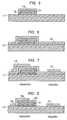
- FIGS. 1-11are schematic representations of the process steps used for forming buried capacitor multi-level printed circuit boards according to the process of the invention.
- a cutaway section 11 of a single level of a laminated PCBis shown with a layer 12 of tantalum deposited on the surface of the board.
- the board 11is shown as a single level at this stage but eventually will become multilevel as will become evident.
- Board 11can also be a multilevel board at this stage to which yet another level is being added in this process.
- the layer 12 of tantalumis deposited by sputtering or other appropriate deposition technique. Sputtering from a DC magnetron source, at a pressure of 5-20 mtorr flowing argon, and a power density of 0,1-2 W/cm 2 , are suitable sputtering conditions. The deposition rate at the high power level is approximately 2250 Angstroms/min. An appropriate thickness range for this layer is 1 to 5 ⁇ m.
- Layer 13 of tantalum nitrideis then deposited over layer 12 as shown in FIG. 2 .
- This layeris optional but does improve adhesion of layers subsequently deposited on the structure.
- a suitable thickness range for layer 13is 1 to 2 ⁇ m.
- Layer 13can be formed in the manner described for layer 12 with the added step of introducing nitrogen in the flowing argon at a concentration in the range 10-30%.
- capacitor materials designated for layer 12 and optional layer 13represents a preferred embodiment.
- Other capacitor materialsmay also be suitable, e.g. Ti, Zr, or Al. These materials can be anodized readily to form the capacitor dielectric as will be described below for the preferred choice, Ta.
- layer 12 , or layers 12 and 13are then lithographically patterned using a photomask 14 to define the first electrode of the capacitor.
- the exposed portions of layer 12 , or layers 12 and 13are removed using a 1:2:4 etch of HF, HNO 3 and water, to give the structure shown in FIG. 4 .
- the next step, represented by FIG. 5,is to form the capacitor dielectric by anodizing the first electrode of the capacitor.
- the board of FIG. 4is placed in an electrolyte of 0.1 wt. % aqueous citric acid, and anodized using a platinum cathode and a voltage that is ramped at constant current for about 10 minutes to reach 100 V, and held for approximately an hour.
- the resulting tantalum oxide filmis approximately 1800 Angstroms. Other suitable techniques or anodizing conditions can be used.
- the objectiveis to form a uniform film in the thickness range 0.05 to 0.5 ⁇ m.
- the second electrodeis formed by blanket depositing a metal layer over the structure as shown in FIG. 6 .
- this layeris aluminum, although other suitable conductor materials can be substituted.
- Aluminummay be DC magnetron sputtered using conditions similar to those given for tantalum sputtering except that higher power levels, i.e. a power density as high as 6 W/cm 2 can be used, which deposits the film at a rate of 1 ⁇ m/min.
- a suitable thickness range for layer 16is 0.3 to 1 ⁇ m.
- layer 16is patterned photolithographically using photomask 17 .
- this stepinvolves the formation of two components, a capacitor as already described, and an inductor to be formed at the site indicated.
- Etchants for aluminumare well known.
- a suitable etchantis PAE available from General Chemical Co., Parsippany, N.J.
- FIG. 8After patterning aluminum layer 16 and removing mask 17 the structure appears as in FIG. 8 .
- the counterelectrode for the capacitoris shown at 18 and a conductive strip which will become the primary element of the inductor is shown at 21 .
- the inductance of the inductoris determined by the dimensions of the spiral strip 21 .
- the formation of multiple components at this stage in the processis an optional feature of the invention.
- the primary focus of the inventionis the formation of the capacitor.
- the element designated 21 for the inductor in this sequencecan be polysilicon, with the objective of forming a buried resistor.
- the polysiliconcan be deposited e.g. by evaporation or CVD, and patterned lithographically. The same steps as described below for the inductor can be used to complete the resistor.
- the resistance valueis determined by choice of the length and cross section of the strip 21 , and/or by modifying the conductivity of the polysilicon by appropriate dopants either during the deposition or with a post deposition implant. It is also convenient and fully compatible with the process as described to form resistors of TaN.
- the electrode 18has two important features that allow effective interconnection to the buried structure.
- the firstis the extended portion 19 that extends beyond the capacitor edge laterally along the surface of the circuit board 11 as shown in FIG. 8 .
- the secondis the termination of the conductor 18 at a point spaced from the edge of the capacitor dielectric, leaving a portion 22 of the capacitor dielectric exposed. This portion will later accommodate electrical interconnection to the underlying capacitor electrode 12 (or optionally 12 and 13 ).
- the importance of the electrode extension 19 , and the exposed insulator portion 22will become apparent in subsequent processing steps.
- the capacitance of the capacitoris primarily determined by the design, i.e. area, of the capacitor plates and the thickness of the capacitor dielectric, but can be further trimmed photolithographically by adjusting the photomask laterally to expose more, or less, of the counterelectrode 18 to be etched away.
- photolithographyin the steps described is the preferred technique. However, some dimensions may be relatively large by lithography standards. Accordingly, some or all the elements may be formed by other techniques, such as lift-off, or even shadow masking.
- a upper circuit board level 23is bonded to the lower circuit board level to form the MPCB.
- the means for bonding the layersis preferably an epoxy layer although other non-conducting adhesive techniques may be found useful. Techniques for joining levels of MPCBs are well knwon.
- the various elements in the figuresare not drawn to scale, which is particularly evident in FIG. 9 .
- the layers of a typical laminate, either rigid or flexible,are substantially thicker than the elements being buried between the layers.
- the inventionwill be most effective with circuit board layers that have a moderate degree of resiliency, e.g. polyimide or other polymer materials.
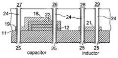
- interconnections to the buried layersare then made, as illustrated in FIG. 10, by forming via holes 24 by standard drilling, and plating the through holes with metal 25 such as copper.
- metal 25such as copper.
- the function of the extended portion 19 of electrode 18 , and the importance of the non-conductive space 22 left by incomplete coverage of aluminum layer over the capacitor dielectric,are evident in this figure.
- surface interconnection 26effectively contacts the lower plate 12 of the capacitor
- surface interconnection 27contacts the electrode tab 19 of the counterelectrode 18 of the capacitor
- surface interconnections 28 and 29contact the buried inductor 21 .
- the geometric configuration of the capacitor platesmay have a variety of forms.
- the capacitor geometry in plan viewis square or rectangular.
- the inductormay also have a variety of shapes, e.g. spiral.
- FIG. 11A plan view of a typical device at the processing stage represented by FIG. 8, i.e. with the components visible, is shown in FIG. 11 .
- the portion 11 of the boardis cutout from the interior of a large board with typical printed circuits, surface mounted active components, etc., not shown.
- the exposed portion 22 of the capacitor dielectricappears in this view, and the geometry of the counterelectrode 18 is also shown.
- the electrode extension 19is shown as a strip with a width equal to that of the capacitor, but it may have a width larger or smaller than the capacitor width.
- the interconnect regions that will later be occupied by through hole interconnections,are shown in phantom at 26-29.
- the width of the capacitorlies in the y-axis as shown and the length of the capacitor extends along the x-axis.
- the effective area of the capacitorhas a first edge 28 , and a second edge 29 parallel to the first edge.
- the contact location 26 in the first contact region 22for interconnecting the lower plate of the capacitor, is spaced from the second edge 29 as shown.
- the extended portion of the electrode 18shown at 19 , extends laterally beyond the first edge 28 of the capacitor along the surface of the printed circuit board level 11 , providing a second contact region 19 for the interconnection location 27 to interconnect the upper plate of the capacitor.
- a printed circuit board levelas meaning a single laminate or other circuit board material in a multi-level circuit board structure.
- the multi-level structuremay be part of a multi-chip module (MCM) or may be a passive interconnect board or flexible circuit.
- MCMmulti-chip module
- through hole interconnectionis meant, consistent with terminology widely used in this art, to refer to the standard plated hole that extends through at least one level of the multi-level printed circuit board so as to interconnect a conductor on one side of said board level to a conductor on the other side of that level, i.e. an interlevel conductor, or to a surface conductor on the other side of the multi-level board.
- the through hole interconnection shown in FIG. 10extends to the surface of the MPCB the interconnection could be between levels in a MPCB with three or more levels.
- the capacitor dielectric in the above descriptionis an oxide formed electrolytically by anodizing the first capacitor electrode according to well known tantalum capacitor technology.
- other dielectricsincluding nitrides or oxynitrides may also be used.
- the dielectricmay be grown by other techniques, e.g. plasma techniques, or it may be deposited by a suitable deposition technique, e.g. CVD.
Landscapes
- Engineering & Computer Science (AREA)
- Microelectronics & Electronic Packaging (AREA)
- Parts Printed On Printed Circuit Boards (AREA)
- Printing Elements For Providing Electric Connections Between Printed Circuits (AREA)
- Fixed Capacitors And Capacitor Manufacturing Machines (AREA)
- Laminated Bodies (AREA)
- Production Of Multi-Layered Print Wiring Board (AREA)
Abstract
Description
Claims (11)
Priority Applications (1)
| Application Number | Priority Date | Filing Date | Title |
|---|---|---|---|
| US09/291,781US6317948B1 (en) | 1997-08-25 | 1999-04-14 | Embedded thin film passive components |
Applications Claiming Priority (2)
| Application Number | Priority Date | Filing Date | Title |
|---|---|---|---|
| US08/918,216US6005197A (en) | 1997-08-25 | 1997-08-25 | Embedded thin film passive components |
| US09/291,781US6317948B1 (en) | 1997-08-25 | 1999-04-14 | Embedded thin film passive components |
Related Parent Applications (1)
| Application Number | Title | Priority Date | Filing Date |
|---|---|---|---|
| US08/918,216DivisionUS6005197A (en) | 1997-08-25 | 1997-08-25 | Embedded thin film passive components |
Publications (1)
| Publication Number | Publication Date |
|---|---|
| US6317948B1true US6317948B1 (en) | 2001-11-20 |
Family
ID=25440001
Family Applications (2)
| Application Number | Title | Priority Date | Filing Date |
|---|---|---|---|
| US08/918,216Expired - LifetimeUS6005197A (en) | 1997-08-25 | 1997-08-25 | Embedded thin film passive components |
| US09/291,781Expired - LifetimeUS6317948B1 (en) | 1997-08-25 | 1999-04-14 | Embedded thin film passive components |
Family Applications Before (1)
| Application Number | Title | Priority Date | Filing Date |
|---|---|---|---|
| US08/918,216Expired - LifetimeUS6005197A (en) | 1997-08-25 | 1997-08-25 | Embedded thin film passive components |
Country Status (4)
| Country | Link |
|---|---|
| US (2) | US6005197A (en) |
| EP (1) | EP0899992B1 (en) |
| JP (1) | JPH11126976A (en) |
| DE (1) | DE69835260T2 (en) |
Cited By (41)
| Publication number | Priority date | Publication date | Assignee | Title |
|---|---|---|---|---|
| US20030151905A1 (en)* | 2002-02-11 | 2003-08-14 | Adc Dsl Systems, Inc. | Electrical connections within substrates |
| US20030172526A1 (en)* | 2002-03-12 | 2003-09-18 | Nitto Denko Corporation | Production method of printed circuit board |
| US20040065471A1 (en)* | 2002-10-07 | 2004-04-08 | The Hong Kong Polytechnic University | Electronic circuit board |
| US20050263321A1 (en)* | 2002-10-07 | 2005-12-01 | The Hong Kong Polytechnic University | Electronic circuit board |
| US20070115702A1 (en)* | 2002-03-05 | 2007-05-24 | Samsung Electronics Co., Ltd. | Device having inductors and capacitors |
| US20070209178A1 (en)* | 2006-03-10 | 2007-09-13 | Motorola, Inc. | Method for forming embedded capacitors on a printed curcuit board and resultant printed circuit board |
| US20080151522A1 (en)* | 2000-09-25 | 2008-06-26 | Ibiden Co., Ltd. | Semiconductor element, method of manufacturing semiconductor element, multi-layer printed circuit board, and method of manufacturing multi-layer printed circuit board |
| US20080190656A1 (en)* | 2004-05-06 | 2008-08-14 | Microbridge Technologies Inc. | Trimming Of Embedded Passive Components Using Pulsed Heating |
| US20090070996A1 (en)* | 2000-02-25 | 2009-03-19 | Ibiden Co., Ltd. | Printed circuit board manufacturing method |
| US7920042B2 (en) | 2007-09-10 | 2011-04-05 | Enpirion, Inc. | Micromagnetic device and method of forming the same |
| US7952459B2 (en) | 2007-09-10 | 2011-05-31 | Enpirion, Inc. | Micromagnetic device and method of forming the same |
| US7955868B2 (en) | 2007-09-10 | 2011-06-07 | Enpirion, Inc. | Method of forming a micromagnetic device |
| US8018315B2 (en) | 2007-09-10 | 2011-09-13 | Enpirion, Inc. | Power converter employing a micromagnetic device |
| US8043544B2 (en) | 2004-11-10 | 2011-10-25 | Enpirion, Inc. | Method of manufacturing an encapsulated package for a magnetic device |
| US20110298554A1 (en)* | 2009-10-01 | 2011-12-08 | Stmicroelectronics Sa | Method of adjustment during manufacture of a circuit having a capacitor |
| US20120030942A1 (en)* | 2010-08-09 | 2012-02-09 | Samsung Electro-Mechanics Co., Ltd. | Method for manufacturing multi-layer printed circuit board |
| US8133529B2 (en) | 2007-09-10 | 2012-03-13 | Enpirion, Inc. | Method of forming a micromagnetic device |
| US8139362B2 (en) | 2005-10-05 | 2012-03-20 | Enpirion, Inc. | Power module with a magnetic device having a conductive clip |
| US8153473B2 (en) | 2008-10-02 | 2012-04-10 | Empirion, Inc. | Module having a stacked passive element and method of forming the same |
| US8266793B2 (en)* | 2008-10-02 | 2012-09-18 | Enpirion, Inc. | Module having a stacked magnetic device and semiconductor device and method of forming the same |
| US8339802B2 (en) | 2008-10-02 | 2012-12-25 | Enpirion, Inc. | Module having a stacked magnetic device and semiconductor device and method of forming the same |
| US8384506B2 (en) | 2005-10-05 | 2013-02-26 | Enpirion, Inc. | Magnetic device having a conductive clip |
| US20130120949A1 (en)* | 2011-11-16 | 2013-05-16 | Tien-Wei SUN | Method of manufacturing passive component module |
| US8528190B2 (en) | 2004-11-10 | 2013-09-10 | Enpirion, Inc. | Method of manufacturing a power module |
| US20130232784A1 (en)* | 2012-03-06 | 2013-09-12 | Ngk Spark Plug Co., Ltd | Method of manufacturing wiring substrate |
| US8541991B2 (en) | 2008-04-16 | 2013-09-24 | Enpirion, Inc. | Power converter with controller operable in selected modes of operation |
| US8631560B2 (en) | 2005-10-05 | 2014-01-21 | Enpirion, Inc. | Method of forming a magnetic device having a conductive clip |
| US8686698B2 (en) | 2008-04-16 | 2014-04-01 | Enpirion, Inc. | Power converter with controller operable in selected modes of operation |
| US8692532B2 (en) | 2008-04-16 | 2014-04-08 | Enpirion, Inc. | Power converter with controller operable in selected modes of operation |
| US8698463B2 (en) | 2008-12-29 | 2014-04-15 | Enpirion, Inc. | Power converter with a dynamically configurable controller based on a power conversion mode |
| US8701272B2 (en) | 2005-10-05 | 2014-04-22 | Enpirion, Inc. | Method of forming a power module with a magnetic device having a conductive clip |
| US8867295B2 (en) | 2010-12-17 | 2014-10-21 | Enpirion, Inc. | Power converter for a memory module |
| US9054086B2 (en) | 2008-10-02 | 2015-06-09 | Enpirion, Inc. | Module having a stacked passive element and method of forming the same |
| US9246390B2 (en) | 2008-04-16 | 2016-01-26 | Enpirion, Inc. | Power converter with controller operable in selected modes of operation |
| US9509217B2 (en) | 2015-04-20 | 2016-11-29 | Altera Corporation | Asymmetric power flow controller for a power converter and method of operating the same |
| US9548714B2 (en) | 2008-12-29 | 2017-01-17 | Altera Corporation | Power converter with a dynamically configurable controller and output filter |
| US20170162603A1 (en)* | 2015-12-02 | 2017-06-08 | Semiconductor Energy Laboratory Co., Ltd. | Semiconductor Device |
| US20180027647A1 (en)* | 2016-07-20 | 2018-01-25 | Hcl Technologies Limited | Interconnection between printed circuit boards |
| US10660193B2 (en)* | 2016-08-03 | 2020-05-19 | Kabushiki Kaisha Toyota Jidoshokki | Multilayer substrate |
| US20210159153A1 (en)* | 2016-12-21 | 2021-05-27 | Dai Nippon Printing Co., Ltd. | Through electrode substrate and semiconductor device |
| US11121123B2 (en) | 2017-12-27 | 2021-09-14 | Murata Manufacturing Co., Ltd. | Semiconductor composite device and package board used therein |
Families Citing this family (44)
| Publication number | Priority date | Publication date | Assignee | Title |
|---|---|---|---|---|
| US6005197A (en)* | 1997-08-25 | 1999-12-21 | Lucent Technologies Inc. | Embedded thin film passive components |
| PL339005A1 (en)* | 1997-08-27 | 2000-12-04 | Pioneer Hi Bred Int | Genes encoding enzymes of lignin synthesis track and their applications |
| EP1014399B1 (en)* | 1998-12-22 | 2006-05-17 | Matsushita Electric Industrial Co., Ltd. | Flexible thin film capacitor and method for producing the same |
| CN101232777B (en) | 1999-09-02 | 2010-06-09 | 伊比登株式会社 | printed wiring board |
| JP4554790B2 (en)* | 1999-09-02 | 2010-09-29 | イビデン株式会社 | Printed wiring board and printed wiring board manufacturing method |
| EP1137332B1 (en) | 1999-09-02 | 2006-11-22 | Ibiden Co., Ltd. | Printed wiring board and method of producing the same and capacitor to be contained in printed wiring board |
| KR100363789B1 (en)* | 1999-12-17 | 2002-12-11 | 삼성전기주식회사 | Manufacturing method of substrate for resonator |
| US20020171530A1 (en)* | 2000-03-30 | 2002-11-21 | Victor Company Of Japan, Limited | Production method of thin film passive element formed on printed circuit board and thin film passive element produced by the method |
| TW471067B (en)* | 2000-08-31 | 2002-01-01 | Advanced Semiconductor Eng | Integrated circuit package board which integrates de-coupled capacitor |
| JP2002198654A (en)* | 2000-12-25 | 2002-07-12 | Kyocera Corp | Wiring board with built-in electric element and method of manufacturing the same |
| US20020158305A1 (en)* | 2001-01-05 | 2002-10-31 | Sidharth Dalmia | Organic substrate having integrated passive components |
| JP3666411B2 (en)* | 2001-05-07 | 2005-06-29 | ソニー株式会社 | High frequency module device |
| JP4810772B2 (en)* | 2001-07-31 | 2011-11-09 | パナソニック株式会社 | Circuit module |
| JP2003158378A (en)* | 2001-11-26 | 2003-05-30 | Hitachi Ltd | Method for manufacturing electronic circuit device having multilayer circuit board |
| US7260890B2 (en)* | 2002-06-26 | 2007-08-28 | Georgia Tech Research Corporation | Methods for fabricating three-dimensional all organic interconnect structures |
| US6987307B2 (en) | 2002-06-26 | 2006-01-17 | Georgia Tech Research Corporation | Stand-alone organic-based passive devices |
| US6900708B2 (en)* | 2002-06-26 | 2005-05-31 | Georgia Tech Research Corporation | Integrated passive devices fabricated utilizing multi-layer, organic laminates |
| US20040108134A1 (en)* | 2002-10-11 | 2004-06-10 | Borland William J. | Printed wiring boards having low inductance embedded capacitors and methods of making same |
| US20040231885A1 (en)* | 2003-03-07 | 2004-11-25 | Borland William J. | Printed wiring boards having capacitors and methods of making thereof |
| US7489914B2 (en)* | 2003-03-28 | 2009-02-10 | Georgia Tech Research Corporation | Multi-band RF transceiver with passive reuse in organic substrates |
| JP2005286112A (en)* | 2004-03-30 | 2005-10-13 | Airex Inc | Printed circuit board and its manufacturing method |
| US7259077B2 (en)* | 2004-04-29 | 2007-08-21 | Sychip Inc. | Integrated passive devices |
| CN100576979C (en)* | 2004-06-25 | 2009-12-30 | 揖斐电株式会社 | Printed wiring board and method for manufacturing same |
| US7100277B2 (en)* | 2004-07-01 | 2006-09-05 | E. I. Du Pont De Nemours And Company | Methods of forming printed circuit boards having embedded thick film capacitors |
| US8345433B2 (en) | 2004-07-08 | 2013-01-01 | Avx Corporation | Heterogeneous organic laminate stack ups for high frequency applications |
| US7186919B2 (en)* | 2004-08-16 | 2007-03-06 | Samsung Electro-Mechanics Co., Ltd. | Printed circuit board including embedded capacitors and method of manufacturing the same |
| TWI315648B (en)* | 2004-11-17 | 2009-10-01 | Phoenix Prec Technology Corp | Circuit board structure with embeded adjustable passive components and method for fabricating the same |
| US20060217102A1 (en)* | 2005-03-22 | 2006-09-28 | Yinon Degani | Cellular/Wi-Fi combination devices |
| US20060220167A1 (en)* | 2005-03-31 | 2006-10-05 | Intel Corporation | IC package with prefabricated film capacitor |
| US20060289976A1 (en)* | 2005-06-23 | 2006-12-28 | Intel Corporation | Pre-patterned thin film capacitor and method for embedding same in a package substrate |
| JP4857642B2 (en)* | 2005-07-29 | 2012-01-18 | Tdk株式会社 | Method for manufacturing thin-film electronic components |
| US20070065964A1 (en)* | 2005-09-22 | 2007-03-22 | Yinon Degani | Integrated passive devices |
| US7936043B2 (en) | 2006-03-17 | 2011-05-03 | Sychip Inc. | Integrated passive device substrates |
| US7439840B2 (en) | 2006-06-27 | 2008-10-21 | Jacket Micro Devices, Inc. | Methods and apparatuses for high-performing multi-layer inductors |
| US7636242B2 (en)* | 2006-06-29 | 2009-12-22 | Intel Corporation | Integrated inductor |
| US7808434B2 (en)* | 2006-08-09 | 2010-10-05 | Avx Corporation | Systems and methods for integrated antennae structures in multilayer organic-based printed circuit devices |
| US7989895B2 (en)* | 2006-11-15 | 2011-08-02 | Avx Corporation | Integration using package stacking with multi-layer organic substrates |
| US20080151513A1 (en)* | 2006-12-21 | 2008-06-26 | Joseph Parchesky | High-frequency PCB connections that utilize blocking capacitors between the pins |
| KR101032342B1 (en)* | 2009-04-24 | 2011-05-02 | 삼화콘덴서공업주식회사 | Embedded Capacitors, Embedded Capacitor Sheets Using the Same, and Manufacturing Method Thereof |
| US8018027B2 (en)* | 2009-10-30 | 2011-09-13 | Murata Manufacturing Co., Ltd. | Flip-bonded dual-substrate inductor, flip-bonded dual-substrate inductor, and integrated passive device including a flip-bonded dual-substrate inductor |
| JP5352437B2 (en)* | 2009-11-30 | 2013-11-27 | ルネサスエレクトロニクス株式会社 | Manufacturing method of semiconductor device |
| JP4957835B2 (en)* | 2010-05-31 | 2012-06-20 | Tdk株式会社 | Thin film electronic component and method for manufacturing thin film electronic component |
| US11714143B2 (en) | 2014-04-24 | 2023-08-01 | Regents Of The University Of California | Omnidirectional MRI catheter resonator and related systems, methods and devices |
| CN105226045B (en) | 2014-05-30 | 2018-07-27 | 日月光半导体制造股份有限公司 | Semiconductor device and manufacturing method thereof |
Citations (6)
| Publication number | Priority date | Publication date | Assignee | Title |
|---|---|---|---|---|
| US4349862A (en)* | 1980-08-11 | 1982-09-14 | International Business Machines Corporation | Capacitive chip carrier and multilayer ceramic capacitors |
| US5530288A (en)* | 1994-10-12 | 1996-06-25 | International Business Machines Corporation | Passive interposer including at least one passive electronic component |
| US5636099A (en)* | 1994-05-31 | 1997-06-03 | Matsushita Electric Industrial Co., Ltd. | Variable capacitor formed by multilayer circuit board |
| US5745334A (en)* | 1996-03-25 | 1998-04-28 | International Business Machines Corporation | Capacitor formed within printed circuit board |
| US5972484A (en)* | 1997-12-01 | 1999-10-26 | Polyeitan Composites Ltd. | Ultrahigh molecular weight polyethylene composite for printed circuit board and antenna base material |
| US6005197A (en)* | 1997-08-25 | 1999-12-21 | Lucent Technologies Inc. | Embedded thin film passive components |
Family Cites Families (2)
| Publication number | Priority date | Publication date | Assignee | Title |
|---|---|---|---|---|
| JP2764745B2 (en)* | 1989-07-21 | 1998-06-11 | オムロン株式会社 | Hybrid circuit board and method of manufacturing the same |
| US5027253A (en)* | 1990-04-09 | 1991-06-25 | Ibm Corporation | Printed circuit boards and cards having buried thin film capacitors and processing techniques for fabricating said boards and cards |
- 1997
- 1997-08-25USUS08/918,216patent/US6005197A/ennot_activeExpired - Lifetime
- 1998
- 1998-08-18DEDE69835260Tpatent/DE69835260T2/ennot_activeExpired - Lifetime
- 1998-08-18EPEP98306562Apatent/EP0899992B1/ennot_activeExpired - Lifetime
- 1998-08-21JPJP10235966Apatent/JPH11126976A/enactivePending
- 1999
- 1999-04-14USUS09/291,781patent/US6317948B1/ennot_activeExpired - Lifetime
Patent Citations (7)
| Publication number | Priority date | Publication date | Assignee | Title |
|---|---|---|---|---|
| US4349862A (en)* | 1980-08-11 | 1982-09-14 | International Business Machines Corporation | Capacitive chip carrier and multilayer ceramic capacitors |
| US5636099A (en)* | 1994-05-31 | 1997-06-03 | Matsushita Electric Industrial Co., Ltd. | Variable capacitor formed by multilayer circuit board |
| US5530288A (en)* | 1994-10-12 | 1996-06-25 | International Business Machines Corporation | Passive interposer including at least one passive electronic component |
| US5770476A (en)* | 1994-10-12 | 1998-06-23 | International Business Machines Corporation | Passive interposer including at least one passive electronic component |
| US5745334A (en)* | 1996-03-25 | 1998-04-28 | International Business Machines Corporation | Capacitor formed within printed circuit board |
| US6005197A (en)* | 1997-08-25 | 1999-12-21 | Lucent Technologies Inc. | Embedded thin film passive components |
| US5972484A (en)* | 1997-12-01 | 1999-10-26 | Polyeitan Composites Ltd. | Ultrahigh molecular weight polyethylene composite for printed circuit board and antenna base material |
Cited By (79)
| Publication number | Priority date | Publication date | Assignee | Title |
|---|---|---|---|---|
| US20090070996A1 (en)* | 2000-02-25 | 2009-03-19 | Ibiden Co., Ltd. | Printed circuit board manufacturing method |
| US8438727B2 (en)* | 2000-02-25 | 2013-05-14 | Ibiden Co., Ltd. | Multilayer printed circuit board and multilayer printed circuit board manufacturing method |
| US8453323B2 (en) | 2000-02-25 | 2013-06-04 | Ibiden Co., Ltd. | Printed circuit board manufacturing method |
| US8186045B2 (en) | 2000-02-25 | 2012-05-29 | Ibiden Co., Ltd. | Multilayer printed circuit board and multilayer printed circuit board manufacturing method |
| US8079142B2 (en) | 2000-02-25 | 2011-12-20 | Ibiden Co., Ltd. | Printed circuit board manufacturing method |
| US8046914B2 (en) | 2000-02-25 | 2011-11-01 | Ibiden Co., Ltd. | Method for manufacturing multilayer printed circuit board |
| US20100031503A1 (en)* | 2000-02-25 | 2010-02-11 | Ibiden Co., Ltd. | Multilayer printed circuit board and multilayer printed circuit board manufacturing method |
| US20100018049A1 (en)* | 2000-02-25 | 2010-01-28 | Ibiden Co., Ltd. | Multilayer printed circuit board and multilayer printed circuit board manufacturing method |
| US20080151522A1 (en)* | 2000-09-25 | 2008-06-26 | Ibiden Co., Ltd. | Semiconductor element, method of manufacturing semiconductor element, multi-layer printed circuit board, and method of manufacturing multi-layer printed circuit board |
| US9245838B2 (en) | 2000-09-25 | 2016-01-26 | Ibiden Co., Ltd. | Semiconductor element |
| US8822323B2 (en) | 2000-09-25 | 2014-09-02 | Ibiden Co., Ltd. | Semiconductor element, method of manufacturing semiconductor element, multi-layer printed circuit board, and method of manufacturing multi-layer printed circuit board |
| US20080206926A1 (en)* | 2000-09-25 | 2008-08-28 | Ibiden Co., Ltd. | Semiconductor element, method of manufacturing semiconductor element, multi-layer printed circuit board, and method of manufacturing multi-layer printed circuit board |
| US8067699B2 (en) | 2000-09-25 | 2011-11-29 | Ibiden Co., Ltd. | Semiconductor element, method of manufacturing semiconductor element, multi-layer printed circuit board, and method of manufacturing multi-layer printed circuit board |
| US8524535B2 (en) | 2000-09-25 | 2013-09-03 | Ibiden Co., Ltd. | Semiconductor element, method of manufacturing semiconductor element, multi-layer printed circuit board, and method of manufacturing multi-layer printed circuit board |
| US8959756B2 (en) | 2000-09-25 | 2015-02-24 | Ibiden Co., Ltd. | Method of manufacturing a printed circuit board having an embedded electronic component |
| US8293579B2 (en) | 2000-09-25 | 2012-10-23 | Ibiden Co., Ltd. | Semiconductor element, method of manufacturing semiconductor element, multi-layer printed circuit board, and method of manufacturing multi-layer printed circuit board |
| US20100140803A1 (en)* | 2000-09-25 | 2010-06-10 | Ibiden Co., Ltd. | Semiconductor element, method of manufacturing semiconductor element, multi-layer printed circuit board, and method of manufacturing multi-layer printed circuit board |
| US20030151905A1 (en)* | 2002-02-11 | 2003-08-14 | Adc Dsl Systems, Inc. | Electrical connections within substrates |
| US7152312B2 (en)* | 2002-02-11 | 2006-12-26 | Adc Dsl Systems, Inc. | Method for transmitting current through a substrate |
| US7939909B2 (en) | 2002-03-05 | 2011-05-10 | Samsung Electronics Co., Ltd. | Device having inductors and capacitors |
| US20070115702A1 (en)* | 2002-03-05 | 2007-05-24 | Samsung Electronics Co., Ltd. | Device having inductors and capacitors |
| CN1316862C (en)* | 2002-03-12 | 2007-05-16 | 日东电工株式会社 | Printed circuit board producing method |
| US20030172526A1 (en)* | 2002-03-12 | 2003-09-18 | Nitto Denko Corporation | Production method of printed circuit board |
| US7007379B2 (en)* | 2002-03-12 | 2006-03-07 | Nitto Denko Corporation | Production method of printed circuit board |
| US7675401B2 (en) | 2002-10-07 | 2010-03-09 | The Hong Kong Polytechnic University | Electronic circuit board |
| US20050263321A1 (en)* | 2002-10-07 | 2005-12-01 | The Hong Kong Polytechnic University | Electronic circuit board |
| US20040065471A1 (en)* | 2002-10-07 | 2004-04-08 | The Hong Kong Polytechnic University | Electronic circuit board |
| US20080190656A1 (en)* | 2004-05-06 | 2008-08-14 | Microbridge Technologies Inc. | Trimming Of Embedded Passive Components Using Pulsed Heating |
| US8043544B2 (en) | 2004-11-10 | 2011-10-25 | Enpirion, Inc. | Method of manufacturing an encapsulated package for a magnetic device |
| US8528190B2 (en) | 2004-11-10 | 2013-09-10 | Enpirion, Inc. | Method of manufacturing a power module |
| US8631560B2 (en) | 2005-10-05 | 2014-01-21 | Enpirion, Inc. | Method of forming a magnetic device having a conductive clip |
| US8139362B2 (en) | 2005-10-05 | 2012-03-20 | Enpirion, Inc. | Power module with a magnetic device having a conductive clip |
| US8701272B2 (en) | 2005-10-05 | 2014-04-22 | Enpirion, Inc. | Method of forming a power module with a magnetic device having a conductive clip |
| US8384506B2 (en) | 2005-10-05 | 2013-02-26 | Enpirion, Inc. | Magnetic device having a conductive clip |
| US10304615B2 (en) | 2005-10-05 | 2019-05-28 | Enpirion, Inc. | Method of forming a power module with a magnetic device having a conductive clip |
| US20070209178A1 (en)* | 2006-03-10 | 2007-09-13 | Motorola, Inc. | Method for forming embedded capacitors on a printed curcuit board and resultant printed circuit board |
| US7444727B2 (en)* | 2006-03-10 | 2008-11-04 | Motorola, Inc. | Method for forming multi-layer embedded capacitors on a printed circuit board |
| US7920042B2 (en) | 2007-09-10 | 2011-04-05 | Enpirion, Inc. | Micromagnetic device and method of forming the same |
| US8618900B2 (en) | 2007-09-10 | 2013-12-31 | Enpirion, Inc. | Micromagnetic device and method of forming the same |
| US7952459B2 (en) | 2007-09-10 | 2011-05-31 | Enpirion, Inc. | Micromagnetic device and method of forming the same |
| US9299489B2 (en) | 2007-09-10 | 2016-03-29 | Enpirion, Inc. | Micromagnetic device and method of forming the same |
| US7955868B2 (en) | 2007-09-10 | 2011-06-07 | Enpirion, Inc. | Method of forming a micromagnetic device |
| US8339232B2 (en) | 2007-09-10 | 2012-12-25 | Enpirion, Inc. | Micromagnetic device and method of forming the same |
| US8018315B2 (en) | 2007-09-10 | 2011-09-13 | Enpirion, Inc. | Power converter employing a micromagnetic device |
| US8133529B2 (en) | 2007-09-10 | 2012-03-13 | Enpirion, Inc. | Method of forming a micromagnetic device |
| US9246390B2 (en) | 2008-04-16 | 2016-01-26 | Enpirion, Inc. | Power converter with controller operable in selected modes of operation |
| US8541991B2 (en) | 2008-04-16 | 2013-09-24 | Enpirion, Inc. | Power converter with controller operable in selected modes of operation |
| US8686698B2 (en) | 2008-04-16 | 2014-04-01 | Enpirion, Inc. | Power converter with controller operable in selected modes of operation |
| US8692532B2 (en) | 2008-04-16 | 2014-04-08 | Enpirion, Inc. | Power converter with controller operable in selected modes of operation |
| US8153473B2 (en) | 2008-10-02 | 2012-04-10 | Empirion, Inc. | Module having a stacked passive element and method of forming the same |
| US8266793B2 (en)* | 2008-10-02 | 2012-09-18 | Enpirion, Inc. | Module having a stacked magnetic device and semiconductor device and method of forming the same |
| US9054086B2 (en) | 2008-10-02 | 2015-06-09 | Enpirion, Inc. | Module having a stacked passive element and method of forming the same |
| US8339802B2 (en) | 2008-10-02 | 2012-12-25 | Enpirion, Inc. | Module having a stacked magnetic device and semiconductor device and method of forming the same |
| US9548714B2 (en) | 2008-12-29 | 2017-01-17 | Altera Corporation | Power converter with a dynamically configurable controller and output filter |
| US8698463B2 (en) | 2008-12-29 | 2014-04-15 | Enpirion, Inc. | Power converter with a dynamically configurable controller based on a power conversion mode |
| US8756778B2 (en)* | 2009-10-01 | 2014-06-24 | Stmicroelectronics Sa | Method of adjustment during manufacture of a circuit having a capacitor |
| US20110298554A1 (en)* | 2009-10-01 | 2011-12-08 | Stmicroelectronics Sa | Method of adjustment during manufacture of a circuit having a capacitor |
| US9060458B2 (en)* | 2010-08-09 | 2015-06-16 | Samsung Electro-Mechanics Co., Ltd. | Method for manufacturing multi-layer printed circuit board |
| US20120030942A1 (en)* | 2010-08-09 | 2012-02-09 | Samsung Electro-Mechanics Co., Ltd. | Method for manufacturing multi-layer printed circuit board |
| US9627028B2 (en) | 2010-12-17 | 2017-04-18 | Enpirion, Inc. | Power converter for a memory module |
| US8867295B2 (en) | 2010-12-17 | 2014-10-21 | Enpirion, Inc. | Power converter for a memory module |
| US9125320B2 (en)* | 2011-11-16 | 2015-09-01 | Dyi-chung Hu | Method of manufacturing passive component module |
| US20130120949A1 (en)* | 2011-11-16 | 2013-05-16 | Tien-Wei SUN | Method of manufacturing passive component module |
| US20130232784A1 (en)* | 2012-03-06 | 2013-09-12 | Ngk Spark Plug Co., Ltd | Method of manufacturing wiring substrate |
| US10084380B2 (en) | 2015-04-20 | 2018-09-25 | Altera Corporation | Asymmetric power flow controller for a power converter and method of operating the same |
| US9509217B2 (en) | 2015-04-20 | 2016-11-29 | Altera Corporation | Asymmetric power flow controller for a power converter and method of operating the same |
| US10714502B2 (en)* | 2015-12-02 | 2020-07-14 | Semiconductor Energy Laboratory Co., Ltd. | Semiconductor device |
| US20170162603A1 (en)* | 2015-12-02 | 2017-06-08 | Semiconductor Energy Laboratory Co., Ltd. | Semiconductor Device |
| US11056510B2 (en) | 2015-12-02 | 2021-07-06 | Semiconductor Energy Laboratory Co., Ltd. | Semiconductor device |
| US11710744B2 (en) | 2015-12-02 | 2023-07-25 | Semiconductor Energy Laboratory Co., Ltd. | Semiconductor device |
| US12396262B2 (en) | 2015-12-02 | 2025-08-19 | Semiconductor Energy Laboratory Co., Ltd. | Semiconductor device |
| US20180027647A1 (en)* | 2016-07-20 | 2018-01-25 | Hcl Technologies Limited | Interconnection between printed circuit boards |
| US10582608B2 (en)* | 2016-07-20 | 2020-03-03 | Hcl Technologies Limited | Interconnection between printed circuit boards |
| US10660193B2 (en)* | 2016-08-03 | 2020-05-19 | Kabushiki Kaisha Toyota Jidoshokki | Multilayer substrate |
| US20210159153A1 (en)* | 2016-12-21 | 2021-05-27 | Dai Nippon Printing Co., Ltd. | Through electrode substrate and semiconductor device |
| US11742273B2 (en)* | 2016-12-21 | 2023-08-29 | Dai Nippon Printing Co., Ltd. | Through electrode substrate and semiconductor device |
| US12136591B2 (en) | 2016-12-21 | 2024-11-05 | Dai Nippon Printing Co., Ltd. | Through electrode substrate and semiconductor device |
| US11121123B2 (en) | 2017-12-27 | 2021-09-14 | Murata Manufacturing Co., Ltd. | Semiconductor composite device and package board used therein |
| US11552020B2 (en) | 2017-12-27 | 2023-01-10 | Murata Manufacturing Co., Ltd. | Semiconductor composite device and package board used therein |
Also Published As
| Publication number | Publication date |
|---|---|
| EP0899992A2 (en) | 1999-03-03 |
| DE69835260D1 (en) | 2006-08-31 |
| US6005197A (en) | 1999-12-21 |
| JPH11126976A (en) | 1999-05-11 |
| DE69835260T2 (en) | 2007-06-06 |
| EP0899992B1 (en) | 2006-07-19 |
| EP0899992A3 (en) | 2000-09-06 |
Similar Documents
| Publication | Publication Date | Title |
|---|---|---|
| US6317948B1 (en) | Embedded thin film passive components | |
| JP3980658B2 (en) | Thin film capacitor forming method, thin film capacitor manufacturing method, thin film bypass capacitor manufacturing method, and thin film capacitor | |
| US3699011A (en) | Method of producing thin film integrated circuits | |
| KR100834833B1 (en) | Capacitor, circuit board with built-in capacitor and method for producting the same | |
| US6356455B1 (en) | Thin integral resistor/capacitor/inductor package, method of manufacture | |
| US6466430B2 (en) | Capacitor | |
| CN1051670C (en) | Laminar stackable circuit board structure and manufacture | |
| US6410858B1 (en) | Multilayered wiring board, a production process for, and semiconductor device using, the same | |
| JP3359865B2 (en) | Electronic interconnect structure and method for manufacturing the same | |
| US6261941B1 (en) | Method for manufacturing a multilayer wiring substrate | |
| KR20030040083A (en) | Process for manufacturing multiple layer wiring substrate onto which thin film capacitor is incorporated | |
| TW360941B (en) | Capacitors in integrated circuits | |
| US6262478B1 (en) | Electronic interconnect structure and method for manufacturing it | |
| JPH09213567A (en) | Thin film capacitor and manufacturing method thereof | |
| US4890192A (en) | Thin film capacitor | |
| WO2007075714A2 (en) | Embedded capacitors and methods for their fabrication and connection | |
| JP2002100533A (en) | Method of forming capacitor element, method of forming composite thin film element, wiring board and module board | |
| US7005722B2 (en) | RC terminator and production method therefor | |
| JP2570607B2 (en) | Method for manufacturing capacitor | |
| JP2737762B2 (en) | Method for manufacturing semiconductor device | |
| DE69827851T2 (en) | Electronic wiring structure | |
| JPH0621651A (en) | Multilayer wiring circuit board and its manufacture | |
| JP2003133669A (en) | Electronic circuit board and method of manufacturing the same | |
| WO2001056086A1 (en) | Rc terminator and production method therefor | |
| JPH1174630A (en) | Structure and manufacturing method of substrate with capacitor |
Legal Events
| Date | Code | Title | Description |
|---|---|---|---|
| AS | Assignment | Owner name:LUCENT TECHNOLOGIES INC., NEW JERSEY Free format text:ASSIGNMENT OF ASSIGNORS INTEREST;ASSIGNORS:KOLA, RATNAJI RAO;MANZIONE, LOUIS THOMAS;WATTS, RODERICK KENT;REEL/FRAME:011409/0001 Effective date:19970820 | |
| STCF | Information on status: patent grant | Free format text:PATENTED CASE | |
| FPAY | Fee payment | Year of fee payment:4 | |
| FPAY | Fee payment | Year of fee payment:8 | |
| FPAY | Fee payment | Year of fee payment:12 | |
| AS | Assignment | Owner name:DEUTSCHE BANK AG NEW YORK BRANCH, AS COLLATERAL AG Free format text:PATENT SECURITY AGREEMENT;ASSIGNORS:LSI CORPORATION;AGERE SYSTEMS LLC;REEL/FRAME:032856/0031 Effective date:20140506 | |
| AS | Assignment | Owner name:AVAGO TECHNOLOGIES GENERAL IP (SINGAPORE) PTE. LTD Free format text:ASSIGNMENT OF ASSIGNORS INTEREST;ASSIGNOR:AGERE SYSTEMS LLC;REEL/FRAME:035365/0634 Effective date:20140804 | |
| AS | Assignment | Owner name:LSI CORPORATION, CALIFORNIA Free format text:TERMINATION AND RELEASE OF SECURITY INTEREST IN PATENT RIGHTS (RELEASES RF 032856-0031);ASSIGNOR:DEUTSCHE BANK AG NEW YORK BRANCH, AS COLLATERAL AGENT;REEL/FRAME:037684/0039 Effective date:20160201 Owner name:AGERE SYSTEMS LLC, PENNSYLVANIA Free format text:TERMINATION AND RELEASE OF SECURITY INTEREST IN PATENT RIGHTS (RELEASES RF 032856-0031);ASSIGNOR:DEUTSCHE BANK AG NEW YORK BRANCH, AS COLLATERAL AGENT;REEL/FRAME:037684/0039 Effective date:20160201 | |
| AS | Assignment | Owner name:BANK OF AMERICA, N.A., AS COLLATERAL AGENT, NORTH CAROLINA Free format text:PATENT SECURITY AGREEMENT;ASSIGNOR:AVAGO TECHNOLOGIES GENERAL IP (SINGAPORE) PTE. LTD.;REEL/FRAME:037808/0001 Effective date:20160201 Owner name:BANK OF AMERICA, N.A., AS COLLATERAL AGENT, NORTH Free format text:PATENT SECURITY AGREEMENT;ASSIGNOR:AVAGO TECHNOLOGIES GENERAL IP (SINGAPORE) PTE. LTD.;REEL/FRAME:037808/0001 Effective date:20160201 | |
| AS | Assignment | Owner name:AVAGO TECHNOLOGIES GENERAL IP (SINGAPORE) PTE. LTD., SINGAPORE Free format text:TERMINATION AND RELEASE OF SECURITY INTEREST IN PATENTS;ASSIGNOR:BANK OF AMERICA, N.A., AS COLLATERAL AGENT;REEL/FRAME:041710/0001 Effective date:20170119 Owner name:AVAGO TECHNOLOGIES GENERAL IP (SINGAPORE) PTE. LTD Free format text:TERMINATION AND RELEASE OF SECURITY INTEREST IN PATENTS;ASSIGNOR:BANK OF AMERICA, N.A., AS COLLATERAL AGENT;REEL/FRAME:041710/0001 Effective date:20170119 | |
| AS | Assignment | Owner name:BELL SEMICONDUCTOR, LLC, ILLINOIS Free format text:ASSIGNMENT OF ASSIGNORS INTEREST;ASSIGNORS:AVAGO TECHNOLOGIES GENERAL IP (SINGAPORE) PTE. LTD.;BROADCOM CORPORATION;REEL/FRAME:044886/0001 Effective date:20171208 | |
| AS | Assignment | Owner name:CORTLAND CAPITAL MARKET SERVICES LLC, AS COLLATERA Free format text:SECURITY INTEREST;ASSIGNORS:HILCO PATENT ACQUISITION 56, LLC;BELL SEMICONDUCTOR, LLC;BELL NORTHERN RESEARCH, LLC;REEL/FRAME:045216/0020 Effective date:20180124 | |
| AS | Assignment | Owner name:BELL NORTHERN RESEARCH, LLC, ILLINOIS Free format text:SECURITY INTEREST;ASSIGNOR:CORTLAND CAPITAL MARKET SERVICES LLC;REEL/FRAME:060885/0001 Effective date:20220401 Owner name:BELL SEMICONDUCTOR, LLC, ILLINOIS Free format text:SECURITY INTEREST;ASSIGNOR:CORTLAND CAPITAL MARKET SERVICES LLC;REEL/FRAME:060885/0001 Effective date:20220401 Owner name:HILCO PATENT ACQUISITION 56, LLC, ILLINOIS Free format text:SECURITY INTEREST;ASSIGNOR:CORTLAND CAPITAL MARKET SERVICES LLC;REEL/FRAME:060885/0001 Effective date:20220401 |