US6316287B1 - Chip scale surface mount packages for semiconductor device and process of fabricating the same - Google Patents
Chip scale surface mount packages for semiconductor device and process of fabricating the sameDownload PDFInfo
- Publication number
- US6316287B1 US6316287B1US09/395,094US39509499AUS6316287B1US 6316287 B1US6316287 B1US 6316287B1US 39509499 AUS39509499 AUS 39509499AUS 6316287 B1US6316287 B1US 6316287B1
- Authority
- US
- United States
- Prior art keywords
- metal layer
- die
- wafer
- metal
- layer
- Prior art date
- Legal status (The legal status is an assumption and is not a legal conclusion. Google has not performed a legal analysis and makes no representation as to the accuracy of the status listed.)
- Expired - Lifetime
Links
Images


Classifications
- H—ELECTRICITY
- H01—ELECTRIC ELEMENTS
- H01L—SEMICONDUCTOR DEVICES NOT COVERED BY CLASS H10
- H01L23/00—Details of semiconductor or other solid state devices
- H01L23/28—Encapsulations, e.g. encapsulating layers, coatings, e.g. for protection
- H01L23/31—Encapsulations, e.g. encapsulating layers, coatings, e.g. for protection characterised by the arrangement or shape
- H01L23/3107—Encapsulations, e.g. encapsulating layers, coatings, e.g. for protection characterised by the arrangement or shape the device being completely enclosed
- H01L23/3114—Encapsulations, e.g. encapsulating layers, coatings, e.g. for protection characterised by the arrangement or shape the device being completely enclosed the device being a chip scale package, e.g. CSP
- H—ELECTRICITY
- H01—ELECTRIC ELEMENTS
- H01L—SEMICONDUCTOR DEVICES NOT COVERED BY CLASS H10
- H01L24/00—Arrangements for connecting or disconnecting semiconductor or solid-state bodies; Methods or apparatus related thereto
- H01L24/01—Means for bonding being attached to, or being formed on, the surface to be connected, e.g. chip-to-package, die-attach, "first-level" interconnects; Manufacturing methods related thereto
- H01L24/10—Bump connectors ; Manufacturing methods related thereto
- H01L24/12—Structure, shape, material or disposition of the bump connectors prior to the connecting process
- H—ELECTRICITY
- H01—ELECTRIC ELEMENTS
- H01L—SEMICONDUCTOR DEVICES NOT COVERED BY CLASS H10
- H01L23/00—Details of semiconductor or other solid state devices
- H01L23/52—Arrangements for conducting electric current within the device in operation from one component to another, i.e. interconnections, e.g. wires, lead frames
- H01L23/538—Arrangements for conducting electric current within the device in operation from one component to another, i.e. interconnections, e.g. wires, lead frames the interconnection structure between a plurality of semiconductor chips being formed on, or in, insulating substrates
- H—ELECTRICITY
- H01—ELECTRIC ELEMENTS
- H01L—SEMICONDUCTOR DEVICES NOT COVERED BY CLASS H10
- H01L24/00—Arrangements for connecting or disconnecting semiconductor or solid-state bodies; Methods or apparatus related thereto
- H01L24/01—Means for bonding being attached to, or being formed on, the surface to be connected, e.g. chip-to-package, die-attach, "first-level" interconnects; Manufacturing methods related thereto
- H01L24/02—Bonding areas ; Manufacturing methods related thereto
- H—ELECTRICITY
- H01—ELECTRIC ELEMENTS
- H01L—SEMICONDUCTOR DEVICES NOT COVERED BY CLASS H10
- H01L24/00—Arrangements for connecting or disconnecting semiconductor or solid-state bodies; Methods or apparatus related thereto
- H01L24/01—Means for bonding being attached to, or being formed on, the surface to be connected, e.g. chip-to-package, die-attach, "first-level" interconnects; Manufacturing methods related thereto
- H01L24/10—Bump connectors ; Manufacturing methods related thereto
- H01L24/11—Manufacturing methods
- H—ELECTRICITY
- H01—ELECTRIC ELEMENTS
- H01L—SEMICONDUCTOR DEVICES NOT COVERED BY CLASS H10
- H01L2224/00—Indexing scheme for arrangements for connecting or disconnecting semiconductor or solid-state bodies and methods related thereto as covered by H01L24/00
- H01L2224/01—Means for bonding being attached to, or being formed on, the surface to be connected, e.g. chip-to-package, die-attach, "first-level" interconnects; Manufacturing methods related thereto
- H01L2224/02—Bonding areas; Manufacturing methods related thereto
- H01L2224/023—Redistribution layers [RDL] for bonding areas
- H01L2224/0231—Manufacturing methods of the redistribution layers
- H—ELECTRICITY
- H01—ELECTRIC ELEMENTS
- H01L—SEMICONDUCTOR DEVICES NOT COVERED BY CLASS H10
- H01L2224/00—Indexing scheme for arrangements for connecting or disconnecting semiconductor or solid-state bodies and methods related thereto as covered by H01L24/00
- H01L2224/01—Means for bonding being attached to, or being formed on, the surface to be connected, e.g. chip-to-package, die-attach, "first-level" interconnects; Manufacturing methods related thereto
- H01L2224/02—Bonding areas; Manufacturing methods related thereto
- H01L2224/023—Redistribution layers [RDL] for bonding areas
- H01L2224/0236—Shape of the insulating layers therebetween
- H—ELECTRICITY
- H01—ELECTRIC ELEMENTS
- H01L—SEMICONDUCTOR DEVICES NOT COVERED BY CLASS H10
- H01L2224/00—Indexing scheme for arrangements for connecting or disconnecting semiconductor or solid-state bodies and methods related thereto as covered by H01L24/00
- H01L2224/01—Means for bonding being attached to, or being formed on, the surface to be connected, e.g. chip-to-package, die-attach, "first-level" interconnects; Manufacturing methods related thereto
- H01L2224/02—Bonding areas; Manufacturing methods related thereto
- H01L2224/023—Redistribution layers [RDL] for bonding areas
- H01L2224/0237—Disposition of the redistribution layers
- H01L2224/02377—Fan-in arrangement
- H—ELECTRICITY
- H01—ELECTRIC ELEMENTS
- H01L—SEMICONDUCTOR DEVICES NOT COVERED BY CLASS H10
- H01L2224/00—Indexing scheme for arrangements for connecting or disconnecting semiconductor or solid-state bodies and methods related thereto as covered by H01L24/00
- H01L2224/01—Means for bonding being attached to, or being formed on, the surface to be connected, e.g. chip-to-package, die-attach, "first-level" interconnects; Manufacturing methods related thereto
- H01L2224/02—Bonding areas; Manufacturing methods related thereto
- H01L2224/04—Structure, shape, material or disposition of the bonding areas prior to the connecting process
- H01L2224/0401—Bonding areas specifically adapted for bump connectors, e.g. under bump metallisation [UBM]
- H—ELECTRICITY
- H01—ELECTRIC ELEMENTS
- H01L—SEMICONDUCTOR DEVICES NOT COVERED BY CLASS H10
- H01L2224/00—Indexing scheme for arrangements for connecting or disconnecting semiconductor or solid-state bodies and methods related thereto as covered by H01L24/00
- H01L2224/01—Means for bonding being attached to, or being formed on, the surface to be connected, e.g. chip-to-package, die-attach, "first-level" interconnects; Manufacturing methods related thereto
- H01L2224/02—Bonding areas; Manufacturing methods related thereto
- H01L2224/04—Structure, shape, material or disposition of the bonding areas prior to the connecting process
- H01L2224/04026—Bonding areas specifically adapted for layer connectors
- H—ELECTRICITY
- H01—ELECTRIC ELEMENTS
- H01L—SEMICONDUCTOR DEVICES NOT COVERED BY CLASS H10
- H01L2224/00—Indexing scheme for arrangements for connecting or disconnecting semiconductor or solid-state bodies and methods related thereto as covered by H01L24/00
- H01L2224/01—Means for bonding being attached to, or being formed on, the surface to be connected, e.g. chip-to-package, die-attach, "first-level" interconnects; Manufacturing methods related thereto
- H01L2224/02—Bonding areas; Manufacturing methods related thereto
- H01L2224/04—Structure, shape, material or disposition of the bonding areas prior to the connecting process
- H01L2224/05—Structure, shape, material or disposition of the bonding areas prior to the connecting process of an individual bonding area
- H01L2224/05001—Internal layers
- H01L2224/05099—Material
- H01L2224/051—Material with a principal constituent of the material being a metal or a metalloid, e.g. boron [B], silicon [Si], germanium [Ge], arsenic [As], antimony [Sb], tellurium [Te] and polonium [Po], and alloys thereof
- H01L2224/05117—Material with a principal constituent of the material being a metal or a metalloid, e.g. boron [B], silicon [Si], germanium [Ge], arsenic [As], antimony [Sb], tellurium [Te] and polonium [Po], and alloys thereof the principal constituent melting at a temperature of greater than or equal to 400°C and less than 950°C
- H01L2224/05124—Aluminium [Al] as principal constituent
- H—ELECTRICITY
- H01—ELECTRIC ELEMENTS
- H01L—SEMICONDUCTOR DEVICES NOT COVERED BY CLASS H10
- H01L2224/00—Indexing scheme for arrangements for connecting or disconnecting semiconductor or solid-state bodies and methods related thereto as covered by H01L24/00
- H01L2224/01—Means for bonding being attached to, or being formed on, the surface to be connected, e.g. chip-to-package, die-attach, "first-level" interconnects; Manufacturing methods related thereto
- H01L2224/02—Bonding areas; Manufacturing methods related thereto
- H01L2224/04—Structure, shape, material or disposition of the bonding areas prior to the connecting process
- H01L2224/05—Structure, shape, material or disposition of the bonding areas prior to the connecting process of an individual bonding area
- H01L2224/05001—Internal layers
- H01L2224/05099—Material
- H01L2224/051—Material with a principal constituent of the material being a metal or a metalloid, e.g. boron [B], silicon [Si], germanium [Ge], arsenic [As], antimony [Sb], tellurium [Te] and polonium [Po], and alloys thereof
- H01L2224/05138—Material with a principal constituent of the material being a metal or a metalloid, e.g. boron [B], silicon [Si], germanium [Ge], arsenic [As], antimony [Sb], tellurium [Te] and polonium [Po], and alloys thereof the principal constituent melting at a temperature of greater than or equal to 950°C and less than 1550°C
- H01L2224/05139—Silver [Ag] as principal constituent
- H—ELECTRICITY
- H01—ELECTRIC ELEMENTS
- H01L—SEMICONDUCTOR DEVICES NOT COVERED BY CLASS H10
- H01L2224/00—Indexing scheme for arrangements for connecting or disconnecting semiconductor or solid-state bodies and methods related thereto as covered by H01L24/00
- H01L2224/01—Means for bonding being attached to, or being formed on, the surface to be connected, e.g. chip-to-package, die-attach, "first-level" interconnects; Manufacturing methods related thereto
- H01L2224/02—Bonding areas; Manufacturing methods related thereto
- H01L2224/04—Structure, shape, material or disposition of the bonding areas prior to the connecting process
- H01L2224/05—Structure, shape, material or disposition of the bonding areas prior to the connecting process of an individual bonding area
- H01L2224/05001—Internal layers
- H01L2224/05099—Material
- H01L2224/051—Material with a principal constituent of the material being a metal or a metalloid, e.g. boron [B], silicon [Si], germanium [Ge], arsenic [As], antimony [Sb], tellurium [Te] and polonium [Po], and alloys thereof
- H01L2224/05138—Material with a principal constituent of the material being a metal or a metalloid, e.g. boron [B], silicon [Si], germanium [Ge], arsenic [As], antimony [Sb], tellurium [Te] and polonium [Po], and alloys thereof the principal constituent melting at a temperature of greater than or equal to 950°C and less than 1550°C
- H01L2224/05144—Gold [Au] as principal constituent
- H—ELECTRICITY
- H01—ELECTRIC ELEMENTS
- H01L—SEMICONDUCTOR DEVICES NOT COVERED BY CLASS H10
- H01L2224/00—Indexing scheme for arrangements for connecting or disconnecting semiconductor or solid-state bodies and methods related thereto as covered by H01L24/00
- H01L2224/01—Means for bonding being attached to, or being formed on, the surface to be connected, e.g. chip-to-package, die-attach, "first-level" interconnects; Manufacturing methods related thereto
- H01L2224/02—Bonding areas; Manufacturing methods related thereto
- H01L2224/04—Structure, shape, material or disposition of the bonding areas prior to the connecting process
- H01L2224/05—Structure, shape, material or disposition of the bonding areas prior to the connecting process of an individual bonding area
- H01L2224/05001—Internal layers
- H01L2224/05099—Material
- H01L2224/051—Material with a principal constituent of the material being a metal or a metalloid, e.g. boron [B], silicon [Si], germanium [Ge], arsenic [As], antimony [Sb], tellurium [Te] and polonium [Po], and alloys thereof
- H01L2224/05138—Material with a principal constituent of the material being a metal or a metalloid, e.g. boron [B], silicon [Si], germanium [Ge], arsenic [As], antimony [Sb], tellurium [Te] and polonium [Po], and alloys thereof the principal constituent melting at a temperature of greater than or equal to 950°C and less than 1550°C
- H01L2224/05147—Copper [Cu] as principal constituent
- H—ELECTRICITY
- H01—ELECTRIC ELEMENTS
- H01L—SEMICONDUCTOR DEVICES NOT COVERED BY CLASS H10
- H01L2224/00—Indexing scheme for arrangements for connecting or disconnecting semiconductor or solid-state bodies and methods related thereto as covered by H01L24/00
- H01L2224/01—Means for bonding being attached to, or being formed on, the surface to be connected, e.g. chip-to-package, die-attach, "first-level" interconnects; Manufacturing methods related thereto
- H01L2224/02—Bonding areas; Manufacturing methods related thereto
- H01L2224/04—Structure, shape, material or disposition of the bonding areas prior to the connecting process
- H01L2224/05—Structure, shape, material or disposition of the bonding areas prior to the connecting process of an individual bonding area
- H01L2224/05001—Internal layers
- H01L2224/05099—Material
- H01L2224/051—Material with a principal constituent of the material being a metal or a metalloid, e.g. boron [B], silicon [Si], germanium [Ge], arsenic [As], antimony [Sb], tellurium [Te] and polonium [Po], and alloys thereof
- H01L2224/05138—Material with a principal constituent of the material being a metal or a metalloid, e.g. boron [B], silicon [Si], germanium [Ge], arsenic [As], antimony [Sb], tellurium [Te] and polonium [Po], and alloys thereof the principal constituent melting at a temperature of greater than or equal to 950°C and less than 1550°C
- H01L2224/05155—Nickel [Ni] as principal constituent
- H—ELECTRICITY
- H01—ELECTRIC ELEMENTS
- H01L—SEMICONDUCTOR DEVICES NOT COVERED BY CLASS H10
- H01L2224/00—Indexing scheme for arrangements for connecting or disconnecting semiconductor or solid-state bodies and methods related thereto as covered by H01L24/00
- H01L2224/01—Means for bonding being attached to, or being formed on, the surface to be connected, e.g. chip-to-package, die-attach, "first-level" interconnects; Manufacturing methods related thereto
- H01L2224/02—Bonding areas; Manufacturing methods related thereto
- H01L2224/04—Structure, shape, material or disposition of the bonding areas prior to the connecting process
- H01L2224/05—Structure, shape, material or disposition of the bonding areas prior to the connecting process of an individual bonding area
- H01L2224/05001—Internal layers
- H01L2224/05099—Material
- H01L2224/051—Material with a principal constituent of the material being a metal or a metalloid, e.g. boron [B], silicon [Si], germanium [Ge], arsenic [As], antimony [Sb], tellurium [Te] and polonium [Po], and alloys thereof
- H01L2224/05163—Material with a principal constituent of the material being a metal or a metalloid, e.g. boron [B], silicon [Si], germanium [Ge], arsenic [As], antimony [Sb], tellurium [Te] and polonium [Po], and alloys thereof the principal constituent melting at a temperature of greater than 1550°C
- H01L2224/05166—Titanium [Ti] as principal constituent
- H—ELECTRICITY
- H01—ELECTRIC ELEMENTS
- H01L—SEMICONDUCTOR DEVICES NOT COVERED BY CLASS H10
- H01L2224/00—Indexing scheme for arrangements for connecting or disconnecting semiconductor or solid-state bodies and methods related thereto as covered by H01L24/00
- H01L2224/01—Means for bonding being attached to, or being formed on, the surface to be connected, e.g. chip-to-package, die-attach, "first-level" interconnects; Manufacturing methods related thereto
- H01L2224/02—Bonding areas; Manufacturing methods related thereto
- H01L2224/04—Structure, shape, material or disposition of the bonding areas prior to the connecting process
- H01L2224/05—Structure, shape, material or disposition of the bonding areas prior to the connecting process of an individual bonding area
- H01L2224/0554—External layer
- H01L2224/05541—Structure
- H01L2224/05548—Bonding area integrally formed with a redistribution layer on the semiconductor or solid-state body
- H—ELECTRICITY
- H01—ELECTRIC ELEMENTS
- H01L—SEMICONDUCTOR DEVICES NOT COVERED BY CLASS H10
- H01L2224/00—Indexing scheme for arrangements for connecting or disconnecting semiconductor or solid-state bodies and methods related thereto as covered by H01L24/00
- H01L2224/01—Means for bonding being attached to, or being formed on, the surface to be connected, e.g. chip-to-package, die-attach, "first-level" interconnects; Manufacturing methods related thereto
- H01L2224/02—Bonding areas; Manufacturing methods related thereto
- H01L2224/04—Structure, shape, material or disposition of the bonding areas prior to the connecting process
- H01L2224/05—Structure, shape, material or disposition of the bonding areas prior to the connecting process of an individual bonding area
- H01L2224/0554—External layer
- H01L2224/05599—Material
- H01L2224/056—Material with a principal constituent of the material being a metal or a metalloid, e.g. boron [B], silicon [Si], germanium [Ge], arsenic [As], antimony [Sb], tellurium [Te] and polonium [Po], and alloys thereof
- H01L2224/05638—Material with a principal constituent of the material being a metal or a metalloid, e.g. boron [B], silicon [Si], germanium [Ge], arsenic [As], antimony [Sb], tellurium [Te] and polonium [Po], and alloys thereof the principal constituent melting at a temperature of greater than or equal to 950°C and less than 1550°C
- H01L2224/05644—Gold [Au] as principal constituent
- H—ELECTRICITY
- H01—ELECTRIC ELEMENTS
- H01L—SEMICONDUCTOR DEVICES NOT COVERED BY CLASS H10
- H01L2224/00—Indexing scheme for arrangements for connecting or disconnecting semiconductor or solid-state bodies and methods related thereto as covered by H01L24/00
- H01L2224/01—Means for bonding being attached to, or being formed on, the surface to be connected, e.g. chip-to-package, die-attach, "first-level" interconnects; Manufacturing methods related thereto
- H01L2224/02—Bonding areas; Manufacturing methods related thereto
- H01L2224/04—Structure, shape, material or disposition of the bonding areas prior to the connecting process
- H01L2224/06—Structure, shape, material or disposition of the bonding areas prior to the connecting process of a plurality of bonding areas
- H01L2224/0601—Structure
- H01L2224/0603—Bonding areas having different sizes, e.g. different heights or widths
- H—ELECTRICITY
- H01—ELECTRIC ELEMENTS
- H01L—SEMICONDUCTOR DEVICES NOT COVERED BY CLASS H10
- H01L2224/00—Indexing scheme for arrangements for connecting or disconnecting semiconductor or solid-state bodies and methods related thereto as covered by H01L24/00
- H01L2224/01—Means for bonding being attached to, or being formed on, the surface to be connected, e.g. chip-to-package, die-attach, "first-level" interconnects; Manufacturing methods related thereto
- H01L2224/10—Bump connectors; Manufacturing methods related thereto
- H01L2224/12—Structure, shape, material or disposition of the bump connectors prior to the connecting process
- H01L2224/13—Structure, shape, material or disposition of the bump connectors prior to the connecting process of an individual bump connector
- H01L2224/13001—Core members of the bump connector
- H01L2224/1302—Disposition
- H01L2224/13024—Disposition the bump connector being disposed on a redistribution layer on the semiconductor or solid-state body
- H—ELECTRICITY
- H01—ELECTRIC ELEMENTS
- H01L—SEMICONDUCTOR DEVICES NOT COVERED BY CLASS H10
- H01L2224/00—Indexing scheme for arrangements for connecting or disconnecting semiconductor or solid-state bodies and methods related thereto as covered by H01L24/00
- H01L2224/01—Means for bonding being attached to, or being formed on, the surface to be connected, e.g. chip-to-package, die-attach, "first-level" interconnects; Manufacturing methods related thereto
- H01L2224/10—Bump connectors; Manufacturing methods related thereto
- H01L2224/12—Structure, shape, material or disposition of the bump connectors prior to the connecting process
- H01L2224/13—Structure, shape, material or disposition of the bump connectors prior to the connecting process of an individual bump connector
- H01L2224/13001—Core members of the bump connector
- H01L2224/13099—Material
- H01L2224/131—Material with a principal constituent of the material being a metal or a metalloid, e.g. boron [B], silicon [Si], germanium [Ge], arsenic [As], antimony [Sb], tellurium [Te] and polonium [Po], and alloys thereof
- H—ELECTRICITY
- H01—ELECTRIC ELEMENTS
- H01L—SEMICONDUCTOR DEVICES NOT COVERED BY CLASS H10
- H01L2224/00—Indexing scheme for arrangements for connecting or disconnecting semiconductor or solid-state bodies and methods related thereto as covered by H01L24/00
- H01L2224/01—Means for bonding being attached to, or being formed on, the surface to be connected, e.g. chip-to-package, die-attach, "first-level" interconnects; Manufacturing methods related thereto
- H01L2224/10—Bump connectors; Manufacturing methods related thereto
- H01L2224/12—Structure, shape, material or disposition of the bump connectors prior to the connecting process
- H01L2224/14—Structure, shape, material or disposition of the bump connectors prior to the connecting process of a plurality of bump connectors
- H01L2224/141—Disposition
- H01L2224/14104—Disposition relative to the bonding areas, e.g. bond pads, of the semiconductor or solid-state body
- H01L2224/1411—Disposition relative to the bonding areas, e.g. bond pads, of the semiconductor or solid-state body the bump connectors being bonded to at least one common bonding area
- H—ELECTRICITY
- H01—ELECTRIC ELEMENTS
- H01L—SEMICONDUCTOR DEVICES NOT COVERED BY CLASS H10
- H01L2224/00—Indexing scheme for arrangements for connecting or disconnecting semiconductor or solid-state bodies and methods related thereto as covered by H01L24/00
- H01L2224/01—Means for bonding being attached to, or being formed on, the surface to be connected, e.g. chip-to-package, die-attach, "first-level" interconnects; Manufacturing methods related thereto
- H01L2224/26—Layer connectors, e.g. plate connectors, solder or adhesive layers; Manufacturing methods related thereto
- H01L2224/28—Structure, shape, material or disposition of the layer connectors prior to the connecting process
- H01L2224/29—Structure, shape, material or disposition of the layer connectors prior to the connecting process of an individual layer connector
- H01L2224/29001—Core members of the layer connector
- H01L2224/2901—Shape
- H01L2224/29012—Shape in top view
- H01L2224/29013—Shape in top view being rectangular or square
- H—ELECTRICITY
- H01—ELECTRIC ELEMENTS
- H01L—SEMICONDUCTOR DEVICES NOT COVERED BY CLASS H10
- H01L2224/00—Indexing scheme for arrangements for connecting or disconnecting semiconductor or solid-state bodies and methods related thereto as covered by H01L24/00
- H01L2224/01—Means for bonding being attached to, or being formed on, the surface to be connected, e.g. chip-to-package, die-attach, "first-level" interconnects; Manufacturing methods related thereto
- H01L2224/26—Layer connectors, e.g. plate connectors, solder or adhesive layers; Manufacturing methods related thereto
- H01L2224/28—Structure, shape, material or disposition of the layer connectors prior to the connecting process
- H01L2224/29—Structure, shape, material or disposition of the layer connectors prior to the connecting process of an individual layer connector
- H01L2224/29001—Core members of the layer connector
- H01L2224/2902—Disposition
- H01L2224/29024—Disposition the layer connector being disposed on a redistribution layer on the semiconductor or solid-state body
- H—ELECTRICITY
- H01—ELECTRIC ELEMENTS
- H01L—SEMICONDUCTOR DEVICES NOT COVERED BY CLASS H10
- H01L2224/00—Indexing scheme for arrangements for connecting or disconnecting semiconductor or solid-state bodies and methods related thereto as covered by H01L24/00
- H01L2224/01—Means for bonding being attached to, or being formed on, the surface to be connected, e.g. chip-to-package, die-attach, "first-level" interconnects; Manufacturing methods related thereto
- H01L2224/26—Layer connectors, e.g. plate connectors, solder or adhesive layers; Manufacturing methods related thereto
- H01L2224/28—Structure, shape, material or disposition of the layer connectors prior to the connecting process
- H01L2224/29—Structure, shape, material or disposition of the layer connectors prior to the connecting process of an individual layer connector
- H01L2224/29001—Core members of the layer connector
- H01L2224/29099—Material
- H01L2224/291—Material with a principal constituent of the material being a metal or a metalloid, e.g. boron [B], silicon [Si], germanium [Ge], arsenic [As], antimony [Sb], tellurium [Te] and polonium [Po], and alloys thereof
- H—ELECTRICITY
- H01—ELECTRIC ELEMENTS
- H01L—SEMICONDUCTOR DEVICES NOT COVERED BY CLASS H10
- H01L2224/00—Indexing scheme for arrangements for connecting or disconnecting semiconductor or solid-state bodies and methods related thereto as covered by H01L24/00
- H01L2224/73—Means for bonding being of different types provided for in two or more of groups H01L2224/10, H01L2224/18, H01L2224/26, H01L2224/34, H01L2224/42, H01L2224/50, H01L2224/63, H01L2224/71
- H01L2224/731—Location prior to the connecting process
- H01L2224/73101—Location prior to the connecting process on the same surface
- H01L2224/73103—Bump and layer connectors
- H—ELECTRICITY
- H01—ELECTRIC ELEMENTS
- H01L—SEMICONDUCTOR DEVICES NOT COVERED BY CLASS H10
- H01L24/00—Arrangements for connecting or disconnecting semiconductor or solid-state bodies; Methods or apparatus related thereto
- H01L24/01—Means for bonding being attached to, or being formed on, the surface to be connected, e.g. chip-to-package, die-attach, "first-level" interconnects; Manufacturing methods related thereto
- H01L24/02—Bonding areas ; Manufacturing methods related thereto
- H01L24/04—Structure, shape, material or disposition of the bonding areas prior to the connecting process
- H01L24/05—Structure, shape, material or disposition of the bonding areas prior to the connecting process of an individual bonding area
- H—ELECTRICITY
- H01—ELECTRIC ELEMENTS
- H01L—SEMICONDUCTOR DEVICES NOT COVERED BY CLASS H10
- H01L24/00—Arrangements for connecting or disconnecting semiconductor or solid-state bodies; Methods or apparatus related thereto
- H01L24/01—Means for bonding being attached to, or being formed on, the surface to be connected, e.g. chip-to-package, die-attach, "first-level" interconnects; Manufacturing methods related thereto
- H01L24/10—Bump connectors ; Manufacturing methods related thereto
- H01L24/12—Structure, shape, material or disposition of the bump connectors prior to the connecting process
- H01L24/13—Structure, shape, material or disposition of the bump connectors prior to the connecting process of an individual bump connector
- H—ELECTRICITY
- H01—ELECTRIC ELEMENTS
- H01L—SEMICONDUCTOR DEVICES NOT COVERED BY CLASS H10
- H01L24/00—Arrangements for connecting or disconnecting semiconductor or solid-state bodies; Methods or apparatus related thereto
- H01L24/01—Means for bonding being attached to, or being formed on, the surface to be connected, e.g. chip-to-package, die-attach, "first-level" interconnects; Manufacturing methods related thereto
- H01L24/26—Layer connectors, e.g. plate connectors, solder or adhesive layers; Manufacturing methods related thereto
- H01L24/28—Structure, shape, material or disposition of the layer connectors prior to the connecting process
- H01L24/29—Structure, shape, material or disposition of the layer connectors prior to the connecting process of an individual layer connector
- H—ELECTRICITY
- H01—ELECTRIC ELEMENTS
- H01L—SEMICONDUCTOR DEVICES NOT COVERED BY CLASS H10
- H01L2924/00—Indexing scheme for arrangements or methods for connecting or disconnecting semiconductor or solid-state bodies as covered by H01L24/00
- H01L2924/0001—Technical content checked by a classifier
- H—ELECTRICITY
- H01—ELECTRIC ELEMENTS
- H01L—SEMICONDUCTOR DEVICES NOT COVERED BY CLASS H10
- H01L2924/00—Indexing scheme for arrangements or methods for connecting or disconnecting semiconductor or solid-state bodies as covered by H01L24/00
- H01L2924/01—Chemical elements
- H01L2924/01004—Beryllium [Be]
- H—ELECTRICITY
- H01—ELECTRIC ELEMENTS
- H01L—SEMICONDUCTOR DEVICES NOT COVERED BY CLASS H10
- H01L2924/00—Indexing scheme for arrangements or methods for connecting or disconnecting semiconductor or solid-state bodies as covered by H01L24/00
- H01L2924/01—Chemical elements
- H01L2924/01005—Boron [B]
- H—ELECTRICITY
- H01—ELECTRIC ELEMENTS
- H01L—SEMICONDUCTOR DEVICES NOT COVERED BY CLASS H10
- H01L2924/00—Indexing scheme for arrangements or methods for connecting or disconnecting semiconductor or solid-state bodies as covered by H01L24/00
- H01L2924/01—Chemical elements
- H01L2924/01006—Carbon [C]
- H—ELECTRICITY
- H01—ELECTRIC ELEMENTS
- H01L—SEMICONDUCTOR DEVICES NOT COVERED BY CLASS H10
- H01L2924/00—Indexing scheme for arrangements or methods for connecting or disconnecting semiconductor or solid-state bodies as covered by H01L24/00
- H01L2924/01—Chemical elements
- H01L2924/01013—Aluminum [Al]
- H—ELECTRICITY
- H01—ELECTRIC ELEMENTS
- H01L—SEMICONDUCTOR DEVICES NOT COVERED BY CLASS H10
- H01L2924/00—Indexing scheme for arrangements or methods for connecting or disconnecting semiconductor or solid-state bodies as covered by H01L24/00
- H01L2924/01—Chemical elements
- H01L2924/01015—Phosphorus [P]
- H—ELECTRICITY
- H01—ELECTRIC ELEMENTS
- H01L—SEMICONDUCTOR DEVICES NOT COVERED BY CLASS H10
- H01L2924/00—Indexing scheme for arrangements or methods for connecting or disconnecting semiconductor or solid-state bodies as covered by H01L24/00
- H01L2924/01—Chemical elements
- H01L2924/01022—Titanium [Ti]
- H—ELECTRICITY
- H01—ELECTRIC ELEMENTS
- H01L—SEMICONDUCTOR DEVICES NOT COVERED BY CLASS H10
- H01L2924/00—Indexing scheme for arrangements or methods for connecting or disconnecting semiconductor or solid-state bodies as covered by H01L24/00
- H01L2924/01—Chemical elements
- H01L2924/01027—Cobalt [Co]
- H—ELECTRICITY
- H01—ELECTRIC ELEMENTS
- H01L—SEMICONDUCTOR DEVICES NOT COVERED BY CLASS H10
- H01L2924/00—Indexing scheme for arrangements or methods for connecting or disconnecting semiconductor or solid-state bodies as covered by H01L24/00
- H01L2924/01—Chemical elements
- H01L2924/01029—Copper [Cu]
- H—ELECTRICITY
- H01—ELECTRIC ELEMENTS
- H01L—SEMICONDUCTOR DEVICES NOT COVERED BY CLASS H10
- H01L2924/00—Indexing scheme for arrangements or methods for connecting or disconnecting semiconductor or solid-state bodies as covered by H01L24/00
- H01L2924/01—Chemical elements
- H01L2924/0103—Zinc [Zn]
- H—ELECTRICITY
- H01—ELECTRIC ELEMENTS
- H01L—SEMICONDUCTOR DEVICES NOT COVERED BY CLASS H10
- H01L2924/00—Indexing scheme for arrangements or methods for connecting or disconnecting semiconductor or solid-state bodies as covered by H01L24/00
- H01L2924/01—Chemical elements
- H01L2924/01033—Arsenic [As]
- H—ELECTRICITY
- H01—ELECTRIC ELEMENTS
- H01L—SEMICONDUCTOR DEVICES NOT COVERED BY CLASS H10
- H01L2924/00—Indexing scheme for arrangements or methods for connecting or disconnecting semiconductor or solid-state bodies as covered by H01L24/00
- H01L2924/01—Chemical elements
- H01L2924/01039—Yttrium [Y]
- H—ELECTRICITY
- H01—ELECTRIC ELEMENTS
- H01L—SEMICONDUCTOR DEVICES NOT COVERED BY CLASS H10
- H01L2924/00—Indexing scheme for arrangements or methods for connecting or disconnecting semiconductor or solid-state bodies as covered by H01L24/00
- H01L2924/01—Chemical elements
- H01L2924/01047—Silver [Ag]
- H—ELECTRICITY
- H01—ELECTRIC ELEMENTS
- H01L—SEMICONDUCTOR DEVICES NOT COVERED BY CLASS H10
- H01L2924/00—Indexing scheme for arrangements or methods for connecting or disconnecting semiconductor or solid-state bodies as covered by H01L24/00
- H01L2924/01—Chemical elements
- H01L2924/01078—Platinum [Pt]
- H—ELECTRICITY
- H01—ELECTRIC ELEMENTS
- H01L—SEMICONDUCTOR DEVICES NOT COVERED BY CLASS H10
- H01L2924/00—Indexing scheme for arrangements or methods for connecting or disconnecting semiconductor or solid-state bodies as covered by H01L24/00
- H01L2924/01—Chemical elements
- H01L2924/01079—Gold [Au]
- H—ELECTRICITY
- H01—ELECTRIC ELEMENTS
- H01L—SEMICONDUCTOR DEVICES NOT COVERED BY CLASS H10
- H01L2924/00—Indexing scheme for arrangements or methods for connecting or disconnecting semiconductor or solid-state bodies as covered by H01L24/00
- H01L2924/01—Chemical elements
- H01L2924/01082—Lead [Pb]
- H—ELECTRICITY
- H01—ELECTRIC ELEMENTS
- H01L—SEMICONDUCTOR DEVICES NOT COVERED BY CLASS H10
- H01L2924/00—Indexing scheme for arrangements or methods for connecting or disconnecting semiconductor or solid-state bodies as covered by H01L24/00
- H01L2924/013—Alloys
- H01L2924/014—Solder alloys
- H—ELECTRICITY
- H01—ELECTRIC ELEMENTS
- H01L—SEMICONDUCTOR DEVICES NOT COVERED BY CLASS H10
- H01L2924/00—Indexing scheme for arrangements or methods for connecting or disconnecting semiconductor or solid-state bodies as covered by H01L24/00
- H01L2924/06—Polymers
- H01L2924/078—Adhesive characteristics other than chemical
- H01L2924/07802—Adhesive characteristics other than chemical not being an ohmic electrical conductor
- H—ELECTRICITY
- H01—ELECTRIC ELEMENTS
- H01L—SEMICONDUCTOR DEVICES NOT COVERED BY CLASS H10
- H01L2924/00—Indexing scheme for arrangements or methods for connecting or disconnecting semiconductor or solid-state bodies as covered by H01L24/00
- H01L2924/10—Details of semiconductor or other solid state devices to be connected
- H01L2924/11—Device type
- H01L2924/13—Discrete devices, e.g. 3 terminal devices
- H01L2924/1304—Transistor
- H01L2924/1305—Bipolar Junction Transistor [BJT]
- H—ELECTRICITY
- H01—ELECTRIC ELEMENTS
- H01L—SEMICONDUCTOR DEVICES NOT COVERED BY CLASS H10
- H01L2924/00—Indexing scheme for arrangements or methods for connecting or disconnecting semiconductor or solid-state bodies as covered by H01L24/00
- H01L2924/10—Details of semiconductor or other solid state devices to be connected
- H01L2924/11—Device type
- H01L2924/13—Discrete devices, e.g. 3 terminal devices
- H01L2924/1304—Transistor
- H01L2924/1306—Field-effect transistor [FET]
- H01L2924/13062—Junction field-effect transistor [JFET]
- H—ELECTRICITY
- H01—ELECTRIC ELEMENTS
- H01L—SEMICONDUCTOR DEVICES NOT COVERED BY CLASS H10
- H01L2924/00—Indexing scheme for arrangements or methods for connecting or disconnecting semiconductor or solid-state bodies as covered by H01L24/00
- H01L2924/10—Details of semiconductor or other solid state devices to be connected
- H01L2924/11—Device type
- H01L2924/13—Discrete devices, e.g. 3 terminal devices
- H01L2924/1304—Transistor
- H01L2924/1306—Field-effect transistor [FET]
- H01L2924/13091—Metal-Oxide-Semiconductor Field-Effect Transistor [MOSFET]
- H—ELECTRICITY
- H01—ELECTRIC ELEMENTS
- H01L—SEMICONDUCTOR DEVICES NOT COVERED BY CLASS H10
- H01L2924/00—Indexing scheme for arrangements or methods for connecting or disconnecting semiconductor or solid-state bodies as covered by H01L24/00
- H01L2924/10—Details of semiconductor or other solid state devices to be connected
- H01L2924/11—Device type
- H01L2924/14—Integrated circuits
- Y—GENERAL TAGGING OF NEW TECHNOLOGICAL DEVELOPMENTS; GENERAL TAGGING OF CROSS-SECTIONAL TECHNOLOGIES SPANNING OVER SEVERAL SECTIONS OF THE IPC; TECHNICAL SUBJECTS COVERED BY FORMER USPC CROSS-REFERENCE ART COLLECTIONS [XRACs] AND DIGESTS
- Y10—TECHNICAL SUBJECTS COVERED BY FORMER USPC
- Y10S—TECHNICAL SUBJECTS COVERED BY FORMER USPC CROSS-REFERENCE ART COLLECTIONS [XRACs] AND DIGESTS
- Y10S438/00—Semiconductor device manufacturing: process
- Y10S438/928—Front and rear surface processing
Definitions
- the resulting integrated circuit (IC) chips or dicemust be separated and packaged in such a way that they can be connected to external circuitry.
- ICintegrated circuit
- packaging techniquesMost involve mounting the die on a leadframe, connecting the die pads to the leadframe by wire-bonding or otherwise, and then encapsulating the die and wire bonds in a plastic capsule, with the leadframe left protruding from the capsule. The encapsulation is often done by injection-molding. The leadframe is then trimmed to remove the tie bars that hold it together, and the leads are bent in such a way that the package can be mounted on a flat surface, typically a printed circuit board (PCB).
- PCBprinted circuit board
- a power MOSFETtypically has its source and gate terminals on the front side of the die and its drain terminal on the back side of the die.
- a vertical diodehas its anode terminal on one face of the die and its cathode terminal on the opposite face of the die.
- Bipolar transistors, junction field effect transistors (JFETs), and various types of integrated circuits (ICs)can also be fabricated in a “vertical” configuration.
- the process of fabricating a semiconductor device package in accordance with this inventionbegins with a semiconductor wafer having a front side and a back side and comprising a plurality of dice separated by scribe lines.
- Each diecomprises a semiconductor device.
- a surface of the front side of each diecomprises a passivation layer and at least one connection pad in electrical contact with a terminal of the semiconductor device.
- the back side of each diemay also be in electrical contact with a terminal of the semiconductor device.
- the processcomprises the following steps: forming a first metal layer in electrical contact with the connection pad, a portion of the first metal layer extending laterally beyond an edge of the die; attaching a cap to the front side of the wafer; cutting through the semiconductor wafer from the back side of the wafer in the scribe line area to form a first cut, the first cut having a first kerf W 1 and exposing a part of the first metal layer; forming a nonconductive layer on the back side of the die; forming a second metal layer, the second metal layer having a first section extending over the nonconductive layer and being in electrical contact with the first metal layer; and cutting through the cap in the scribe line area to form a second cut having a second kerf W 2 that is less than the first kerf W 1 , the second cut leaving in place an area of contact between the first and second metal layers.
- the processalso includes forming a second section of the second metal layer in electrical contact with the backside of the semiconductor wafer, the first and second sections of the second metal layer being electrically insulated from each other.
- the processmay also include grinding, lapping or etching the back side of the semiconductor wafer to reduce the thickness of the wafer after attaching the cap to the front side of the wafer.
- the inventionincludes a process for making an electrical connection between a first location on a first side of a semiconductor die and a second location on a second side of the semiconductor die.
- the processcommences while the die is a part of a semiconductor wafer.
- the processcomprises forming a first metal layer extending laterally from the first location on the first side of the die to an area of the wafer beyond an edge of the die; attaching a cap to the first side of the wafer; cutting through the semiconductor wafer from the second side of the wafer to expose a part of the first metal layer; forming a second metal layer extending laterally from the second location on the second side of the die and along an edge of the die to a region of contact with the first metal layer beyond the edge of the die; and cutting through the cap while leaving intact the region of contact between the first and second metal layers.
- This inventionalso includes package for a semiconductor device.
- the packagecomprises a cap having a width X 1 ; a semiconductor die containing a semiconductor device, the die being attached to the cap with a front side of the die facing the cap and a back side of the die facing away from the cap, the die having a width X 2 that is less than X 1 ; a connection pad in electrical contact with the semiconductor device, the contact being located between the die and the cap and having a width no greater than X 2 ; a first metal layer in electrical contact with the connection pad, a first portion of the first metal layer being located between the connection pad and the cap and a second portion of the first metal layer extending laterally beyond an edge of the connection pad; a second metal layer having first and second sections, the first section of the second metal layer being in contact with the second portion of the first metal layer, the second section being in electrical contact with the backside of the wafer, the first and second sections of the second metal layer being electrically insulated from each other.
- this inventionincludes a package for a semiconductor device comprising a semiconductor die containing a semiconductor device, a first side of the die comprising a connection pad; a cap attached to the first side of the die, an edge of the cap extending laterally beyond an edge of the die; a first metal layer in electrical contact with the connection pad, the first metal layer extending laterally and terminating in a first flange beyond an edge of the die; and a second metal layer extending from a second side of the die and along an edge of the die and terminating in a second flange beyond the edge of the die, the second flange being in contact with the first flange.
- Semiconductor packages according to this inventiondo not require an epoxy capsule or bond wires; the substrate attached to the die serves to protect the die and acts as a heat sink for the die; the packages are very small (e.g., 50% the size of molded packages) and thin; they provide a very low on-resistance for the semiconductor device, particularly if the wafer is ground thinner; they are economical to produce, since they require no molds or lead frames; and they can be used for a wide variety of semiconductor devices such as diodes, MOSFETs, JFETs, bipolar transistors and various types of integrated circuit chips.
- FIG. 1illustrates a top view of a semiconductor wafer.
- FIGS. 2A-2B through 4 A- 4 B, 5 , 6 , and 7 A- 7 B through 12 A- 12 Billustrate the steps of a process of fabricating a semiconductor package in accordance with this invention.
- FIG. 13illustrates a cross-sectional view of a semiconductor package in accordance with this invention.
- FIG. 14illustrates an embodiment of the semiconductor package which includes solder balls.
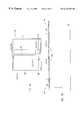
- FIG. 1shows a top view of a semiconductor wafer 100 which contains dice 100 A, 100 B through 100 N.
- wafer 100would contain hundreds or thousands of dice.
- the individual diceare separated by a perpendicular network of scribe lines, with scribe lines 108 running in the Y direction and scribe lines 110 running in the X direction.
- Metal pads for connecting to external circuit elementsare located on the top surface of each of the dice 100 A- 100 N.
- each diehas a source connection pad 106 S and a gate connection pad 106 G.
- Wafer 100is typically has a thickness in the range of 15-30 mils.
- Wafer 100is typically silicon but it could also be another semiconductor material such as silicon carbide or gallium arsenide.
- dice 100 A- 100 Nmust be packaged in a form that allows them to be connected to external circuitry.
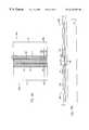
- FIGS. 2A-2B through 4 A- 4 B, 5 , 6 , and 7 A- 7 B through 12 A- 12 Bshow dice 100 A and 100 B that are part of semiconductor wafer 100 .
- the figure labeled “A”is taken from a top or bottom view of the wafer;
- the figure labeled “B”is a cross-sectional view taken at the section labeled “B—B” in the “A” figure.
- the waferis attached to a “cap”, the front side of the wafer normally facing the cap.
- the waferis positioned under the cap, although at some points in the process the structure may be inverted, with the cap under the wafer.
- “above”, “below”, “over”, “under” and other similar termsrefer to the package in its finished form with the cap above the wafer.
- This inventionwill be described with respect to a package for a vertical power MOSFET, which typically has source and gate terminals on its front side and a drain terminal on its back side. It should be understood, however, that the broad principles of this invention can be used to fabricate a package for any type of semiconductor die which has one or more terminals on both its front and back sides or on its front side alone.
- the “front side” of a die or waferrefers to the side of the die or wafer on which the electrical devices and/or a majority of the connection pads are located; “back side” refers to the opposite side of the die or wafer.
- the directional arrow labeled “Z”points to the front side of the wafer and identifies the drawings in which the wafer is inverted.
- each diesince dice 100 A and 100 B contain power MOSFETs (shown symbolically), each die has a gate metal layer 102 G and a source metal layer 102 S overlying the top surface of the silicon or other semiconductor material. Gate metal layers 102 G and source metal layers 102 S are in electrical contact with the gate and source terminals (not shown), respectively, of the power MOSFETs within dice 100 A and 100 B. In FIG. 2A, the separation between layers 102 G and 102 S is shown by the dashed lines.
- metal layers 102 G and 102 Sinclude aluminum, although copper layers are also being used.
- metal layers 102 G and 102 Sneed to be modified so that they will adhere to a solder metal such as tin/lead, for the reasons described below. If there is a native oxide layer on the metal, this native oxide layer must first be removed. Then a solderable metal, such as gold, nickel or silver, is deposited on the exposed metal. The removal of the oxide layer and deposition of a solderable metal can be accomplished by means of a number of known processes. For example, an aluminum layer can be sputter-etched to remove the native aluminum oxide layer and then gold, silver or nickel can be sputtered onto the aluminum.
- the diecan be dipped in a liquid etchant to strip away the oxide layer and the solderable metal can then be deposited by electroless or electrolytic plating.
- Electroless platingincludes the use of a “zyering” process to displace the oxide, followed by the plating of nickel to displace the zincate.
- metal layers 102 G and 102 Sinclude a 3 ⁇ m sublayer of Al overlain by a 1,000 ⁇ TiN sublayer and a 500 ⁇ Ti sublayer.
- a passivation layer 104overlies a portion of gate metal layers 102 G and source metal layers 102 S, and openings in passivation layer 104 define gate connection pads 106 G and source connection pads 106 S.
- Passivation layer 104can be formed of phosphosilicate glass (PSG) 1 mil thick, for example.
- Dice 100 A and 100 Bare separated by a Y-scribe line 108 , which can be 6 mils wide.
- X-scribe lines 110 perpendicular to scribe line 108 at the top and bottom of dice 100 A and 100 Bcan be 4 mils wide.
- a sublayer 202 of titaniumis sputtered onto the front side of wafer 100 , and a sublayer 204 of aluminum is sputtered over the titanium sublayer 202 .
- titanium sublayer 202may be 500 ⁇ thick and aluminum sublayer 204 may be 3 ⁇ m thick.
- Sublayers 202 and 204are then masked and etched, using conventional photolithographic and etching processes, so that the portions of sublayers 202 and 204 shown in FIGS. 3A-3B remain.
- Portions 202 G, 204 G of sublayers 202 , 204cover the gate connection pads 106 G and portions 202 S, 204 S of sublayers 202 , 204 cover the source connection pads 106 S.
- Portions 202 G, 204 Gare electrically insulated from portions 202 S, 204 S.
- the sublayers 202 G, 202 S and 204 G, 204 Sextend laterally into the area of Y-scribe line 108 .
- a 10 ⁇ m nickel sublayer 206is then plated electrolessly onto the top surface of aluminum sublayers 204 G and 204 S and a 0.1 ⁇ m gold sublayer 208 is plated on nickel sublayer 206 .
- the resulting structureis shown in FIGS. 4A-4B, with portions 206 G and 208 G of sublayers 206 and 208 , respectively, overlying gate connection pads 106 G and portions 206 S and 208 S of sublayers 206 and 208 , respectively, overlying source connection pads 106 S.
- Portions 206 G, 208 Gare electrically insulated from portions 206 S, 208 S.
- first metal layer 209can include fewer or more than four sublayers, and the sublayers can be deposited by any of the known processes such as sputtering, evaporation, electroless or electrolytic plating, stencil printing or screen-printing.
- Sublayers 202 , 204 , 206 and 208will sometimes be referred to herein collectively as “first metal layer 209 ”.
- a cap 212is attached to the front side of wafer 100 with a nonconductive adhesive layer 210 .
- Layer 210can be 25 ⁇ m thick and can be an epoxy.
- Cap 212can be made of glass, plastic or copper and can be 250-500 ⁇ m thick. This structure is shown in FIG. 5, with wafer 100 being inverted from the previous drawings and cap 212 being shown below wafer 100 .
- wafer 100is then optionally ground from its back side to a thickness of 3-4 mils or as thin as is possible without damaging the internal microstructure of the semiconductor devices within the dice (which can be, for example, trench-gated MOSFETs).
- a grinding machineavailable from Strausbaugh can be used. This is possible because of the support provided by cap 212 . Grinding reduces the resistance to current flow from the front side to the back side of wafer 100 .
- wafer 100can be thinned by lapping or etching the back side of the wafer.
- a cutis then made along Y-scribe line 108 from the back side of wafer 100 , leaving a thickness of about 1 mil of silicon at the location of the cut.
- the kerf of the saw cutis indicated as W 1 .
- the remaining thickness of siliconis then etched, using a known silicon etchant, to expose the portion of the first metal layer 209 that extends into the area of Y-scribe line 108 .
- the titanium sublayer 202is initially exposed.
- the cutdoes not extend all the way through the first metal layer 209 to the adhesive layer 210 and cap 212 .
- the resulting structureis shown in FIGS. 7A and 7B.
- An insulating layer 214which can be made of polyimide, PSG, nonconductive epoxy, or another nonconductive material, is deposited on the back side of wafer 100 .
- Insulating layer 214can be deposited by spin-coating, dispensing or screen-printing and can be 1 mil thick. Insulating layer 214 is masked and etched, using normal photolithographic and etching techniques, so that portions of insulating layer 214 overlying the first metal layer 209 and portions of the backside of the wafer 100 are removed, as shown in FIGS. 8A and 8B.
- an insulating layere.g., a passivation layer
- a sublayer 216 of titaniumis sputtered onto the back side of wafer 100 , and a sublayer 218 of aluminum is sputtered over the titanium sublayer 216 .
- titanium sublayer 216may be 500 ⁇ thick and aluminum sublayer 218 may be 3 ⁇ m thick.
- Sublayers 216 and 218are then masked and etched, using conventional photolithographic and etching processes, so that the portions of sublayers 216 and 218 shown in FIGS. 9A and 9B remain.
- Sections 216 G, 218 G of sublayers 216 , 218contact the first metal layers 209 in the scribe line area 108 , and by means of the first metal layers 209 sections 216 G, 218 G are in electrical contact with the gate connection pads 106 G.
- Sections 216 S, 218 S of sublayers 216 , 218contact the first metal layers 209 in the scribe line area 108 and by means of the first metal layers 209 are in electrical contact with the source connection pads 106 S.
- Sections 216 D, 218 D of sublayers 216 , 218contact the back side of dice 100 A and 100 B which represent the drain terminals of the MOSFETs.
- Sections 216 G, 218 G and 216 S, 218 Sextend over insulating layer 214 on the back side of dice 100 A and 100 B. Sections 216 G, 218 G and 216 S, 218 S and 216 D, 218 D are electrically insulated from each other.
- a 10 ⁇ m nickel sublayer 220is then plated electrolessly onto the top surface of aluminum sublayers 218 G, 218 S and 218 D, and a 0.1 ⁇ m gold sublayer 222 is plated on nickel sublayer 220 .
- the resulting structureis shown in FIGS. 10A and 10B, with sections 220 G and 222 G of sublayers 220 and 222 , respectively, overlying sections 216 G, 218 G; sections 220 S and 222 S of sublayers 220 and 222 , respectively, overlying sections 216 S, 218 S; and sections 220 D and 222 D of sublayers 220 and 222 , respectively, overlying sections 216 D, 218 D.
- the second metal layer 223can include fewer or more than four sublayers, and the sublayers can be deposited by any of the known processes such as sputtering, evaporation, electroless or electrolytic plating, or screen-printing.
- Sublayers 216 , 218 , 220 and 222will sometimes be referred to herein collectively as “second metal layer 223 ”.
- solder pasteis screen-printed on the second metal layers 224 and then reflowed to form solder posts 224 G, 224 S and 224 D.
- the solder pastecan be 4-5 mils thick.
- Solder posts 224 G, 224 S and 224 Dare electrically insulated from each other. Solder balls, studs, or layers can be used in place of solder posts.
- dice 100 A and 100 Bare separated by saw-cutting cap 212 along Y-scribe line 108 , preferably in the same direction as the first cut, from the back side to the front side of the dice.
- the kerf of the cut (W 2 )is less than W 1 so that the portions of the first and second metal layers 209 , 223 that extend into the scribe line area are left in place.
- the diceare also separated along the X-scribe lines 110 .
- cap 212can be cut using other known processes such as photolithographic patterning and etching.
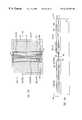
- the resulting semiconductor package 226including die 100 A, is shown in the cross-sectional view of FIG. 13 .
- Package 226is oriented with a cap 212 A over die 100 A.
- cap 212 Ahas a width X 1 .
- Die 100 Ais attached to cap 212 A, with a front side of die 100 A facing cap 212 A and a back side of 100 A die facing away from cap 212 A.
- Die 100 Ahas a width X 2 that is less than X 1 .
- Connection pad 106 Gis in electrical contact with the semiconductor device within die 100 A.
- the gate metal layer 102 G and gate connection pad 106 Gare located between die 100 A and cap 212 A.
- the first metal layer 209is in electrical contact with gate connection pad 106 G.
- a first section 209 A of the first metal layer 209is located between gate metal layer 102 G and cap 212 A, and a second section 209 B of the first metal layer 209 extends laterally beyond the edge of gate metal layer 102 G.
- a second metal layer 223has first and second sections 223 A and 223 B.
- the first section 223 A of the second metal layer 223is in contact with the second section 209 B of the first metal layer 209 at a location beyond the edge of the die 100 A and is insulated from the back side of die 100 A by insulating layer 214 .
- the first section 223 A of the second metal layer 223also includes a slanted portion 223 X that extends at an oblique angle along the edge of the die 100 A.
- the second section 223 B of the second metal layer 223is in electrical contact with the backside of the die 100 A.
- first metal layer 209terminates in a first “flange” 209 F which extends beyond the edge of the die 100 A, and that the second metal layer extends along the edge of the die 100 A and terminates in a second “flange” 223 F beyond the edge of the die 100 A, and that the first and second flanges 209 F, 223 F are in contact with each other and extend longitudinally outward from die 100 A in a direction parallel to the sides of die 100 A.
- Package 226can easily be mounted on, for example, a PCB using solder posts 224 G and 224 D. Solder post 224 S is not shown in FIG. 13 but it too would be connected to the PCB so that the source, gate, and drain terminals of the MOSFET would be connected to the external circuitry. The drain terminal is on the back side of die 100 A and is electrically connected via section 223 B of second metal layer 223 . Package 226 contains no wire bonds and, as has been shown, can be manufactured in a batch process using the entire wafer.
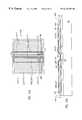
- FIG. 14shows an embodiment of semiconductor package 226 which includes solder balls 230 instead of solder posts.
- the solder ballsmay be applied in a conventional manner by depositing and reflowing solder paste or by other processes such as screen-printing or solder jetting (using, for example, equipment available from Pac Tech GmbH, Am Sch Siemenshorst 15-17, 14641 Nauen, Germany), or by using the wafer level solder ball mounter available from Shibuya Kogyo Co., Ltd., Mameda-Honmachi, Kanazawa 920-8681, Japan.
- Conductive polymer bumpsare another alternative, using for example thermosetting polymers, B-state adhesives, or thermoplastic polymers.
Landscapes
- Engineering & Computer Science (AREA)
- Microelectronics & Electronic Packaging (AREA)
- Computer Hardware Design (AREA)
- Power Engineering (AREA)
- Physics & Mathematics (AREA)
- Condensed Matter Physics & Semiconductors (AREA)
- General Physics & Mathematics (AREA)
- Manufacturing & Machinery (AREA)
- Internal Circuitry In Semiconductor Integrated Circuit Devices (AREA)
- Dicing (AREA)
Abstract
Description
Claims (43)
Priority Applications (8)
| Application Number | Priority Date | Filing Date | Title |
|---|---|---|---|
| US09/395,094US6316287B1 (en) | 1999-09-13 | 1999-09-13 | Chip scale surface mount packages for semiconductor device and process of fabricating the same |
| KR1019990055094AKR100569479B1 (en) | 1999-09-13 | 1999-12-06 | Chip scale surface mount packages for semiconductor device and process of fabricating the same |
| JP34742599AJP2001085367A (en) | 1999-09-13 | 1999-12-07 | Package for semiconductor device having foot print subsutantially the same size as that of semiconductor die, and manufactring process |
| CNB991261232ACN1320617C (en) | 1999-09-13 | 1999-12-13 | Semiconductor device chip scale surface assembling and packaging, and mfg. method therefor |
| EP19990125343EP1085569A3 (en) | 1999-09-13 | 1999-12-21 | Chip scale surface mount packages for semiconductor device and process of fabricating the same |
| TW088120331ATW442854B (en) | 1999-09-13 | 2000-01-07 | Chip scale surface mount packages for semiconductor device and process of fabricating the same |
| SG200000518ASG92671A1 (en) | 1999-09-13 | 2000-01-26 | Chip scale surface mount packages for semiconductor device and process of fabricating the same |
| US09/792,217US20010009298A1 (en) | 1999-09-13 | 2001-02-23 | Chip scale surface mount packages for semiconductor device |
Applications Claiming Priority (1)
| Application Number | Priority Date | Filing Date | Title |
|---|---|---|---|
| US09/395,094US6316287B1 (en) | 1999-09-13 | 1999-09-13 | Chip scale surface mount packages for semiconductor device and process of fabricating the same |
Related Child Applications (1)
| Application Number | Title | Priority Date | Filing Date |
|---|---|---|---|
| US09/792,217DivisionUS20010009298A1 (en) | 1999-09-13 | 2001-02-23 | Chip scale surface mount packages for semiconductor device |
Publications (1)
| Publication Number | Publication Date |
|---|---|
| US6316287B1true US6316287B1 (en) | 2001-11-13 |
Family
ID=23561662
Family Applications (2)
| Application Number | Title | Priority Date | Filing Date |
|---|---|---|---|
| US09/395,094Expired - LifetimeUS6316287B1 (en) | 1999-09-13 | 1999-09-13 | Chip scale surface mount packages for semiconductor device and process of fabricating the same |
| US09/792,217AbandonedUS20010009298A1 (en) | 1999-09-13 | 2001-02-23 | Chip scale surface mount packages for semiconductor device |
Family Applications After (1)
| Application Number | Title | Priority Date | Filing Date |
|---|---|---|---|
| US09/792,217AbandonedUS20010009298A1 (en) | 1999-09-13 | 2001-02-23 | Chip scale surface mount packages for semiconductor device |
Country Status (7)
| Country | Link |
|---|---|
| US (2) | US6316287B1 (en) |
| EP (1) | EP1085569A3 (en) |
| JP (1) | JP2001085367A (en) |
| KR (1) | KR100569479B1 (en) |
| CN (1) | CN1320617C (en) |
| SG (1) | SG92671A1 (en) |
| TW (1) | TW442854B (en) |
Cited By (37)
| Publication number | Priority date | Publication date | Assignee | Title |
|---|---|---|---|---|
| US20030235991A1 (en)* | 2002-06-21 | 2003-12-25 | Schulte Donald W. | Substrate etch method and device |
| US20040070087A1 (en)* | 2002-10-11 | 2004-04-15 | Siliconware Precision Industries Co., Ltd. | Semiconductor package with enhanced chip groundability and method of fabricating the same |
| US20040238926A1 (en)* | 2003-03-20 | 2004-12-02 | Seiko Epson Corporation | Semiconductor wafer, semiconductor device and method for manufacturing same, circuit board, and electronic apparatus |
| US20040251545A1 (en)* | 2003-06-10 | 2004-12-16 | Su Tao | Semiconductor chip with bumps and method for manufacturing the same |
| US20050048740A1 (en)* | 2003-08-06 | 2005-03-03 | Sanyo Electric Co., Ltd. | Semiconductor device and manufacturing method thereof |
| US20050067680A1 (en)* | 2003-09-30 | 2005-03-31 | Boon Suan Jeung | Castellated chip-scale packages and methods for fabricating the same |
| US20050079686A1 (en)* | 2002-02-19 | 2005-04-14 | Infineon Technologies Ag | Method for producing a cover, method for producing a packaged device |
| US20050181580A1 (en)* | 2004-02-16 | 2005-08-18 | Ryuichi Neki | Method for manufacturing mesa semiconductor device |
| US20060081976A1 (en)* | 2003-09-30 | 2006-04-20 | Patel Chirag S | Fabrication of semiconductor dies with micro-pins and structures produced therewith |
| US20060208351A1 (en)* | 2002-06-18 | 2006-09-21 | Poo Chia Y | Semiconductor devices including peripherally located bond pads, intermediates thereof, and assemblies and packages including the semiconductor devices |
| US20070026639A1 (en)* | 2002-10-30 | 2007-02-01 | Sanyo Electric Co., Ltd. | Manufacturing method of semiconductor device |
| US20070063340A1 (en)* | 2005-07-01 | 2007-03-22 | King Owyang | Complete power management system implemented in a single surface mount package |
| US7226809B2 (en) | 2002-06-18 | 2007-06-05 | Micron Technology, Inc. | Semiconductor devices and semiconductor device components with peripherally located, castellated contacts, assemblies and packages including such semiconductor devices or packages and associated methods |
| US20070235774A1 (en)* | 1999-09-13 | 2007-10-11 | Vishay-Siliconix | Chip scale surface mount package for semiconductor device and process of fabricating the same |
| US20080116573A1 (en)* | 2006-11-17 | 2008-05-22 | Mangrum Marc A | Method of packaging a device having a multi-contact elastomer connector contact area and device thereof |
| US20080116560A1 (en)* | 2006-11-17 | 2008-05-22 | Mangrum Marc A | Method of packaging a device having a tangible element and device thereof |
| US20080203513A1 (en)* | 2002-11-19 | 2008-08-28 | Sanyo Electric Co., Ltd. | Semiconductor Integrated Device Having Solid-State Image Sensor Packaged Within and Production Method for Same |
| US20080265424A1 (en)* | 2002-06-18 | 2008-10-30 | Sanyo Electric Co., Ltd. | Semiconductor device |
| US7476563B2 (en) | 2006-11-17 | 2009-01-13 | Freescale Semiconductor, Inc. | Method of packaging a device using a dielectric layer |
| US20090174055A1 (en)* | 2000-06-09 | 2009-07-09 | Vishay-Siliconix | Leadless Semiconductor Packages |
| US7608919B1 (en) | 2003-09-04 | 2009-10-27 | University Of Notre Dame Du Lac | Interconnect packaging systems |
| US20090286390A1 (en)* | 2006-11-17 | 2009-11-19 | Freescale Semiconductor, Inc. | Method of packaging a semiconductor device and a prefabricated connector |
| US20100140753A1 (en)* | 2005-04-08 | 2010-06-10 | Hembree David R | Stacked Semiconductor Component Having Through Wire Interconnect And Method Of Fabrication |
| US20100221854A1 (en)* | 2009-03-02 | 2010-09-02 | Infineon Technologies Ag | Semiconductor device |
| US7795115B2 (en) | 2005-12-28 | 2010-09-14 | Sanyo Electric Co., Ltd. | Method of manufacturing semiconductor device |
| US20110024745A1 (en)* | 2006-04-24 | 2011-02-03 | Hembree David R | System With Semiconductor Components Having Encapsulated Through Wire Interconnects (TWI) |
| US7951702B2 (en)* | 2005-05-19 | 2011-05-31 | Micron Technology, Inc. | Methods for fabricating semiconductor components with conductive interconnects having planar surfaces |
| US8105856B2 (en)* | 2002-04-23 | 2012-01-31 | Semiconductor Components Industries, Llc | Method of manufacturing semiconductor device with wiring on side surface thereof |
| US20120119354A1 (en)* | 2010-11-11 | 2012-05-17 | Taiwan Semiconductor Manufacturing Company, Ltd. | Protecting Flip-Chip Package using Pre-Applied Fillet |
| US8193646B2 (en) | 2005-12-07 | 2012-06-05 | Micron Technology, Inc. | Semiconductor component having through wire interconnect (TWI) with compressed wire |
| US8362606B2 (en) | 2010-07-29 | 2013-01-29 | Alpha & Omega Semiconductor, Inc. | Wafer level chip scale package |
| US8883562B2 (en) | 2007-07-27 | 2014-11-11 | Tessera, Inc. | Reconstituted wafer stack packaging with after-applied pad extensions |
| US8999810B2 (en) | 2006-10-10 | 2015-04-07 | Tessera, Inc. | Method of making a stacked microelectronic package |
| US9048234B2 (en) | 2006-10-10 | 2015-06-02 | Tessera, Inc. | Off-chip vias in stacked chips |
| US9620473B1 (en) | 2013-01-18 | 2017-04-11 | University Of Notre Dame Du Lac | Quilt packaging system with interdigitated interconnecting nodules for inter-chip alignment |
| USRE46549E1 (en)* | 1999-11-26 | 2017-09-12 | Conversant Intellectual Property Management Inc. | Integrated circuit chip having anti-moisture-absorption film at edge thereof and method of forming anti-moisture-absorption film |
| US11239171B2 (en) | 2019-11-07 | 2022-02-01 | Samsung Electronics Co., Ltd. | Semiconductor device and semiconductor package including the same |
Families Citing this family (5)
| Publication number | Priority date | Publication date | Assignee | Title |
|---|---|---|---|---|
| JP4342832B2 (en) | 2003-05-16 | 2009-10-14 | 株式会社東芝 | Semiconductor device and manufacturing method thereof |
| US6768189B1 (en)* | 2003-06-04 | 2004-07-27 | Northrop Grumman Corporation | High power chip scale package |
| JP4349278B2 (en)* | 2004-12-24 | 2009-10-21 | セイコーエプソン株式会社 | Manufacturing method of semiconductor device |
| US8053280B2 (en)* | 2007-11-02 | 2011-11-08 | Infineon Technologies Ag | Method of producing multiple semiconductor devices |
| CN109830890B (en)* | 2019-01-15 | 2021-10-22 | 华天慧创科技(西安)有限公司 | Chip module, wafer-level chip packaging structure and packaging method |
Citations (8)
| Publication number | Priority date | Publication date | Assignee | Title |
|---|---|---|---|---|
| US5270261A (en) | 1991-09-13 | 1993-12-14 | International Business Machines Corporation | Three dimensional multichip package methods of fabrication |
| WO1998019337A1 (en) | 1996-10-29 | 1998-05-07 | Trusi Technologies, Llc | Integrated circuits and methods for their fabrication |
| US5753529A (en) | 1994-05-05 | 1998-05-19 | Siliconix Incorporated | Surface mount and flip chip technology for total integrated circuit isolation |
| US5767578A (en) | 1994-10-12 | 1998-06-16 | Siliconix Incorporated | Surface mount and flip chip technology with diamond film passivation for total integated circuit isolation |
| US5888884A (en)* | 1998-01-02 | 1999-03-30 | General Electric Company | Electronic device pad relocation, precision placement, and packaging in arrays |
| US5998238A (en)* | 1994-10-26 | 1999-12-07 | Mitsubishi Denki Kabushiki Kaisha | Method of fabricating semiconductor device |
| US6153448A (en)* | 1997-05-14 | 2000-11-28 | Kabushiki Kaisha Toshiba | Semiconductor device manufacturing method |
| US6159767A (en)* | 1996-05-20 | 2000-12-12 | Epic Technologies, Inc. | Single chip modules, repairable multichip modules, and methods of fabrication thereof |
Family Cites Families (3)
| Publication number | Priority date | Publication date | Assignee | Title |
|---|---|---|---|---|
| US5910687A (en)* | 1997-01-24 | 1999-06-08 | Chipscale, Inc. | Wafer fabrication of die-bottom contacts for electronic devices |
| US6051489A (en)* | 1997-05-13 | 2000-04-18 | Chipscale, Inc. | Electronic component package with posts on the active side of the substrate |
| JPH1167960A (en)* | 1997-08-20 | 1999-03-09 | Nec Corp | Semiconductor package and mounting board thereof |
- 1999
- 1999-09-13USUS09/395,094patent/US6316287B1/ennot_activeExpired - Lifetime
- 1999-12-06KRKR1019990055094Apatent/KR100569479B1/ennot_activeExpired - Fee Related
- 1999-12-07JPJP34742599Apatent/JP2001085367A/enactivePending
- 1999-12-13CNCNB991261232Apatent/CN1320617C/ennot_activeExpired - Fee Related
- 1999-12-21EPEP19990125343patent/EP1085569A3/ennot_activeWithdrawn
- 2000
- 2000-01-07TWTW088120331Apatent/TW442854B/ennot_activeIP Right Cessation
- 2000-01-26SGSG200000518Apatent/SG92671A1/enunknown
- 2001
- 2001-02-23USUS09/792,217patent/US20010009298A1/ennot_activeAbandoned
Patent Citations (9)
| Publication number | Priority date | Publication date | Assignee | Title |
|---|---|---|---|---|
| US5270261A (en) | 1991-09-13 | 1993-12-14 | International Business Machines Corporation | Three dimensional multichip package methods of fabrication |
| US5753529A (en) | 1994-05-05 | 1998-05-19 | Siliconix Incorporated | Surface mount and flip chip technology for total integrated circuit isolation |
| US5757081A (en) | 1994-05-05 | 1998-05-26 | Siliconix Incorporated | Surface mount and flip chip technology for total integrated circuit isolation |
| US5767578A (en) | 1994-10-12 | 1998-06-16 | Siliconix Incorporated | Surface mount and flip chip technology with diamond film passivation for total integated circuit isolation |
| US5998238A (en)* | 1994-10-26 | 1999-12-07 | Mitsubishi Denki Kabushiki Kaisha | Method of fabricating semiconductor device |
| US6159767A (en)* | 1996-05-20 | 2000-12-12 | Epic Technologies, Inc. | Single chip modules, repairable multichip modules, and methods of fabrication thereof |
| WO1998019337A1 (en) | 1996-10-29 | 1998-05-07 | Trusi Technologies, Llc | Integrated circuits and methods for their fabrication |
| US6153448A (en)* | 1997-05-14 | 2000-11-28 | Kabushiki Kaisha Toshiba | Semiconductor device manufacturing method |
| US5888884A (en)* | 1998-01-02 | 1999-03-30 | General Electric Company | Electronic device pad relocation, precision placement, and packaging in arrays |
Non-Patent Citations (2)
| Title |
|---|
| Lawrence Kren, "The Race For Less Space", Machine Design, Jul. 8, 1999, pp. 86-89. |
| Patrick Mannion, "MOSFETs Break Out Of The Shackles Of Wirebonding", Electronic Design, Mar. 22, 1999, vol. 47, No. 6, pp. 1-5. |
Cited By (90)
| Publication number | Priority date | Publication date | Assignee | Title |
|---|---|---|---|---|
| US7589396B2 (en) | 1999-09-13 | 2009-09-15 | Vishay-Siliconix | Chip scale surface mount package for semiconductor device and process of fabricating the same |
| US20070235774A1 (en)* | 1999-09-13 | 2007-10-11 | Vishay-Siliconix | Chip scale surface mount package for semiconductor device and process of fabricating the same |
| USRE46549E1 (en)* | 1999-11-26 | 2017-09-12 | Conversant Intellectual Property Management Inc. | Integrated circuit chip having anti-moisture-absorption film at edge thereof and method of forming anti-moisture-absorption film |
| US20090174055A1 (en)* | 2000-06-09 | 2009-07-09 | Vishay-Siliconix | Leadless Semiconductor Packages |
| US8928157B2 (en) | 2000-06-09 | 2015-01-06 | Vishay-Siliconix | Encapsulation techniques for leadless semiconductor packages |
| US7288435B2 (en)* | 2002-02-19 | 2007-10-30 | Infineon Technologies Ag | Method for producing a cover, method for producing a packaged device |
| US20050079686A1 (en)* | 2002-02-19 | 2005-04-14 | Infineon Technologies Ag | Method for producing a cover, method for producing a packaged device |
| US8105856B2 (en)* | 2002-04-23 | 2012-01-31 | Semiconductor Components Industries, Llc | Method of manufacturing semiconductor device with wiring on side surface thereof |
| US20060208351A1 (en)* | 2002-06-18 | 2006-09-21 | Poo Chia Y | Semiconductor devices including peripherally located bond pads, intermediates thereof, and assemblies and packages including the semiconductor devices |
| US7226809B2 (en) | 2002-06-18 | 2007-06-05 | Micron Technology, Inc. | Semiconductor devices and semiconductor device components with peripherally located, castellated contacts, assemblies and packages including such semiconductor devices or packages and associated methods |
| US7719102B2 (en) | 2002-06-18 | 2010-05-18 | Sanyo Electric Co., Ltd. | Semiconductor device |
| US20080265424A1 (en)* | 2002-06-18 | 2008-10-30 | Sanyo Electric Co., Ltd. | Semiconductor device |
| US7285850B2 (en) | 2002-06-18 | 2007-10-23 | Micron Technology, Inc. | Support elements for semiconductor devices with peripherally located bond pads |
| US20060208350A1 (en)* | 2002-06-18 | 2006-09-21 | Poo Chia Y | Support elements for semiconductor devices with peripherally located bond pads |
| US6933237B2 (en)* | 2002-06-21 | 2005-08-23 | Hewlett-Packard Development Company, L.P. | Substrate etch method and device |
| US20030235991A1 (en)* | 2002-06-21 | 2003-12-25 | Schulte Donald W. | Substrate etch method and device |
| US20040070087A1 (en)* | 2002-10-11 | 2004-04-15 | Siliconware Precision Industries Co., Ltd. | Semiconductor package with enhanced chip groundability and method of fabricating the same |
| US6903441B2 (en) | 2002-10-11 | 2005-06-07 | Siliconware Precision Industries, Ltd. | Semiconductor package with enhanced chip groundability and method of fabricating the same |
| US20070026639A1 (en)* | 2002-10-30 | 2007-02-01 | Sanyo Electric Co., Ltd. | Manufacturing method of semiconductor device |
| US7662670B2 (en) | 2002-10-30 | 2010-02-16 | Sanyo Electric Co., Ltd. | Manufacturing method of semiconductor device |
| US7619292B2 (en)* | 2002-11-19 | 2009-11-17 | Sanyo Electric Co., Ltd. | Semiconductor integrated device having solid-state image sensor packaged within and production method for same |
| US20080203513A1 (en)* | 2002-11-19 | 2008-08-28 | Sanyo Electric Co., Ltd. | Semiconductor Integrated Device Having Solid-State Image Sensor Packaged Within and Production Method for Same |
| US20040238926A1 (en)* | 2003-03-20 | 2004-12-02 | Seiko Epson Corporation | Semiconductor wafer, semiconductor device and method for manufacturing same, circuit board, and electronic apparatus |
| US20060183313A1 (en)* | 2003-06-10 | 2006-08-17 | Su Tao | Semiconductor package and method for manufacturing the same |
| US7321168B2 (en) | 2003-06-10 | 2008-01-22 | Advanced Semiconductor Engineering, Inc. | Semiconductor package and method for manufacturing the same |
| US20040251545A1 (en)* | 2003-06-10 | 2004-12-16 | Su Tao | Semiconductor chip with bumps and method for manufacturing the same |
| US7037759B2 (en)* | 2003-06-10 | 2006-05-02 | Advanced Semiconductor Engineering, Inc. | Semiconductor package and method for manufacturing the same |
| US20050048740A1 (en)* | 2003-08-06 | 2005-03-03 | Sanyo Electric Co., Ltd. | Semiconductor device and manufacturing method thereof |
| US20080093708A1 (en)* | 2003-08-06 | 2008-04-24 | Sanyo Electric Co., Ltd. | Semiconductor device and manufacturing method thereof |
| US7312107B2 (en)* | 2003-08-06 | 2007-12-25 | Sanyo Electric Co., Ltd. | Semiconductor device and manufacturing method thereof |
| US7919875B2 (en) | 2003-08-06 | 2011-04-05 | Sanyo Electric Co., Ltd. | Semiconductor device with recess portion over pad electrode |
| US10410989B2 (en) | 2003-09-04 | 2019-09-10 | University Of Notre Dame Du Lac | Inter-chip alignment |
| US7612443B1 (en) | 2003-09-04 | 2009-11-03 | University Of Notre Dame Du Lac | Inter-chip communication |
| US8021965B1 (en) | 2003-09-04 | 2011-09-20 | University Of Norte Dame Du Lac | Inter-chip communication |
| US8623700B1 (en) | 2003-09-04 | 2014-01-07 | University Of Notre Dame Du Lac | Inter-chip communication |
| US7608919B1 (en) | 2003-09-04 | 2009-10-27 | University Of Notre Dame Du Lac | Interconnect packaging systems |
| US8063493B2 (en) | 2003-09-30 | 2011-11-22 | Micron Technology, Inc. | Semiconductor device assemblies and packages |
| US7208335B2 (en)* | 2003-09-30 | 2007-04-24 | Micron Technology, Inc. | Castellated chip-scale packages and methods for fabricating the same |
| US7633159B2 (en) | 2003-09-30 | 2009-12-15 | Micron Technology, Inc. | Semiconductor device assemblies and packages with edge contacts and sacrificial substrates and other intermediate structures used or formed in fabricating the assemblies or packages |
| US20050067680A1 (en)* | 2003-09-30 | 2005-03-31 | Boon Suan Jeung | Castellated chip-scale packages and methods for fabricating the same |
| US20100072603A1 (en)* | 2003-09-30 | 2010-03-25 | Micron Technology, Inc. | Semiconductor device assemblies and packages with edge contacts and sacrificial substrates and other intermediate structures used or formed in fabricating the assemblies or packages |
| US20060081976A1 (en)* | 2003-09-30 | 2006-04-20 | Patel Chirag S | Fabrication of semiconductor dies with micro-pins and structures produced therewith |
| US20060006521A1 (en)* | 2003-09-30 | 2006-01-12 | Boon Suan J | Semiconductor device assemblies and packages with edge contacts and sacrificial substrates and other intermediate structures used or formed in fabricating the assemblies or packages |
| US20050181580A1 (en)* | 2004-02-16 | 2005-08-18 | Ryuichi Neki | Method for manufacturing mesa semiconductor device |
| US7192848B2 (en)* | 2004-02-16 | 2007-03-20 | Rohm Co., Ltd. | Method for manufacturing mesa semiconductor device |
| US20100140753A1 (en)* | 2005-04-08 | 2010-06-10 | Hembree David R | Stacked Semiconductor Component Having Through Wire Interconnect And Method Of Fabrication |
| US7919846B2 (en) | 2005-04-08 | 2011-04-05 | Micron Technology, Inc. | Stacked semiconductor component having through wire interconnect |
| US8053909B2 (en) | 2005-04-08 | 2011-11-08 | Micron Technology, Inc. | Semiconductor component having through wire interconnect with compressed bump |
| US8546931B2 (en) | 2005-05-19 | 2013-10-01 | Micron Technology, Inc. | Stacked semiconductor components having conductive interconnects |
| US7951702B2 (en)* | 2005-05-19 | 2011-05-31 | Micron Technology, Inc. | Methods for fabricating semiconductor components with conductive interconnects having planar surfaces |
| US20070063341A1 (en)* | 2005-07-01 | 2007-03-22 | King Owyang | Complete power management system implemented in a single surface mount package |
| US8471381B2 (en) | 2005-07-01 | 2013-06-25 | Vishay-Siliconix | Complete power management system implemented in a single surface mount package |
| US20070063340A1 (en)* | 2005-07-01 | 2007-03-22 | King Owyang | Complete power management system implemented in a single surface mount package |
| US9093359B2 (en) | 2005-07-01 | 2015-07-28 | Vishay-Siliconix | Complete power management system implemented in a single surface mount package |
| US20100219519A1 (en)* | 2005-07-01 | 2010-09-02 | King Owyang | Complete power management system implemented in a single surface mount package |
| US8928138B2 (en) | 2005-07-01 | 2015-01-06 | Vishay-Siliconix | Complete power management system implemented in a single surface mount package |
| US8193646B2 (en) | 2005-12-07 | 2012-06-05 | Micron Technology, Inc. | Semiconductor component having through wire interconnect (TWI) with compressed wire |
| US8513797B2 (en) | 2005-12-07 | 2013-08-20 | Micron Technology, Inc. | Stacked semiconductor component having through wire interconnect (TWI) with compressed wire |
| US9013044B2 (en) | 2005-12-07 | 2015-04-21 | Micron Technology, Inc. | Through wire interconnect (TWI) for semiconductor components having wire in via and bonded connection with substrate contact |
| US7795115B2 (en) | 2005-12-28 | 2010-09-14 | Sanyo Electric Co., Ltd. | Method of manufacturing semiconductor device |
| US8120167B2 (en) | 2006-04-24 | 2012-02-21 | Micron Technology, Inc. | System with semiconductor components having encapsulated through wire interconnects (TWI) |
| US8217510B2 (en) | 2006-04-24 | 2012-07-10 | Micron Technology, Inc. | Semiconductor module system having stacked components with encapsulated through wire interconnects (TWI) |
| US9018751B2 (en) | 2006-04-24 | 2015-04-28 | Micron Technology, Inc. | Semiconductor module system having encapsulated through wire interconnect (TWI) |
| US8404523B2 (en) | 2006-04-24 | 2013-03-26 | Micron Technoloy, Inc. | Method for fabricating stacked semiconductor system with encapsulated through wire interconnects (TWI) |
| US20110024745A1 (en)* | 2006-04-24 | 2011-02-03 | Hembree David R | System With Semiconductor Components Having Encapsulated Through Wire Interconnects (TWI) |
| US8581387B1 (en) | 2006-04-24 | 2013-11-12 | Micron Technology, Inc. | Through wire interconnect (TWI) having bonded connection and encapsulating polymer layer |
| US8741667B2 (en) | 2006-04-24 | 2014-06-03 | Micron Technology, Inc. | Method for fabricating a through wire interconnect (TWI) on a semiconductor substrate having a bonded connection and an encapsulating polymer layer |
| US9048234B2 (en) | 2006-10-10 | 2015-06-02 | Tessera, Inc. | Off-chip vias in stacked chips |
| US9378967B2 (en) | 2006-10-10 | 2016-06-28 | Tessera, Inc. | Method of making a stacked microelectronic package |
| US9899353B2 (en) | 2006-10-10 | 2018-02-20 | Tessera, Inc. | Off-chip vias in stacked chips |
| US8999810B2 (en) | 2006-10-10 | 2015-04-07 | Tessera, Inc. | Method of making a stacked microelectronic package |
| US7476563B2 (en) | 2006-11-17 | 2009-01-13 | Freescale Semiconductor, Inc. | Method of packaging a device using a dielectric layer |
| US7696016B2 (en) | 2006-11-17 | 2010-04-13 | Freescale Semiconductor, Inc. | Method of packaging a device having a tangible element and device thereof |
| US7807511B2 (en) | 2006-11-17 | 2010-10-05 | Freescale Semiconductor, Inc. | Method of packaging a device having a multi-contact elastomer connector contact area and device thereof |
| US20080116573A1 (en)* | 2006-11-17 | 2008-05-22 | Mangrum Marc A | Method of packaging a device having a multi-contact elastomer connector contact area and device thereof |
| US20080116560A1 (en)* | 2006-11-17 | 2008-05-22 | Mangrum Marc A | Method of packaging a device having a tangible element and device thereof |
| US7655502B2 (en) | 2006-11-17 | 2010-02-02 | Freescale Semiconductor, Inc. | Method of packaging a semiconductor device and a prefabricated connector |
| US20090286390A1 (en)* | 2006-11-17 | 2009-11-19 | Freescale Semiconductor, Inc. | Method of packaging a semiconductor device and a prefabricated connector |
| US8883562B2 (en) | 2007-07-27 | 2014-11-11 | Tessera, Inc. | Reconstituted wafer stack packaging with after-applied pad extensions |
| US8323996B2 (en)* | 2009-03-02 | 2012-12-04 | Infineon Technologies Ag | Semiconductor device |
| US20100221854A1 (en)* | 2009-03-02 | 2010-09-02 | Infineon Technologies Ag | Semiconductor device |
| US8362606B2 (en) | 2010-07-29 | 2013-01-29 | Alpha & Omega Semiconductor, Inc. | Wafer level chip scale package |
| US8890296B2 (en) | 2010-07-29 | 2014-11-18 | Alpha And Omega Semiconductor Incorporated | Wafer level chip scale package |
| US20120119354A1 (en)* | 2010-11-11 | 2012-05-17 | Taiwan Semiconductor Manufacturing Company, Ltd. | Protecting Flip-Chip Package using Pre-Applied Fillet |
| US9064881B2 (en)* | 2010-11-11 | 2015-06-23 | Taiwan Semiconductor Manufacturing Company, Ltd. | Protecting flip-chip package using pre-applied fillet |
| US9620414B2 (en) | 2010-11-11 | 2017-04-11 | Taiwan Semiconductor Manufacturing Company, Ltd. | Protecting flip-chip package using pre-applied fillet |
| US9620473B1 (en) | 2013-01-18 | 2017-04-11 | University Of Notre Dame Du Lac | Quilt packaging system with interdigitated interconnecting nodules for inter-chip alignment |
| US11239171B2 (en) | 2019-11-07 | 2022-02-01 | Samsung Electronics Co., Ltd. | Semiconductor device and semiconductor package including the same |
| US11694963B2 (en) | 2019-11-07 | 2023-07-04 | Samsung Electronics Co., Ltd. | Semiconductor device and semiconductor package including the same |
| US11996367B2 (en) | 2019-11-07 | 2024-05-28 | Samsung Electronics Co., Ltd. | Semiconductor device and semiconductor package including the same |
Also Published As
| Publication number | Publication date |
|---|---|
| TW442854B (en) | 2001-06-23 |
| KR100569479B1 (en) | 2006-04-07 |
| KR20010029428A (en) | 2001-04-06 |
| EP1085569A3 (en) | 2003-04-02 |
| US20010009298A1 (en) | 2001-07-26 |
| JP2001085367A (en) | 2001-03-30 |
| CN1320617C (en) | 2007-06-06 |
| SG92671A1 (en) | 2002-11-19 |
| EP1085569A2 (en) | 2001-03-21 |
| CN1288257A (en) | 2001-03-21 |
Similar Documents
| Publication | Publication Date | Title |
|---|---|---|
| US6316287B1 (en) | Chip scale surface mount packages for semiconductor device and process of fabricating the same | |
| US6562647B2 (en) | Chip scale surface mount package for semiconductor device and process of fabricating the same | |
| US6441475B2 (en) | Chip scale surface mount package for semiconductor device and process of fabricating the same | |
| US7589396B2 (en) | Chip scale surface mount package for semiconductor device and process of fabricating the same | |
| US9824949B2 (en) | Packaging solutions for devices and systems comprising lateral GaN power transistors | |
| US7838978B2 (en) | Semiconductor device | |
| US20250157857A1 (en) | Component and method of manufacturing a component using an ultrathin carrier | |
| US10049994B2 (en) | Contact pads with sidewall spacers and method of making contact pads with sidewall spacers | |
| US8736062B2 (en) | Pad sidewall spacers and method of making pad sidewall spacers | |
| US20240213202A1 (en) | Encapsulant-defined land grid array (lga) package and method for making the same | |
| JP2000100864A (en) | Semiconductor device and assembly thereof | |
| HK1034806A (en) | Chip scale surface mount packages for semiconductor device and process of fabricating the same | |
| HK1034805B (en) | Chip scale surface mount package for semiconductor device and process of fabricating the same |
Legal Events
| Date | Code | Title | Description |
|---|---|---|---|
| AS | Assignment | Owner name:VISHAY INTERTECHNOLOGY, INC., PENNSYLVANIA Free format text:ASSIGNMENT OF ASSIGNORS INTEREST;ASSIGNORS:ZANDMAN, FELIX;KASEM, Y. MOHAMMED;HO, YUEH-SE;REEL/FRAME:010669/0366;SIGNING DATES FROM 20000209 TO 20000222 | |
| STCF | Information on status: patent grant | Free format text:PATENTED CASE | |
| FPAY | Fee payment | Year of fee payment:4 | |
| FPAY | Fee payment | Year of fee payment:8 | |
| AS | Assignment | Owner name:COMERICA BANK, AS AGENT,MICHIGAN Free format text:SECURITY AGREEMENT;ASSIGNORS:VISHAY SPRAGUE, INC., SUCCESSOR IN INTEREST TO VISHAY EFI, INC. AND VISHAY THIN FILM, LLC;VISHAY DALE ELECTRONICS, INC.;VISHAY INTERTECHNOLOGY, INC.;AND OTHERS;REEL/FRAME:024006/0515 Effective date:20100212 Owner name:COMERICA BANK, AS AGENT, MICHIGAN Free format text:SECURITY AGREEMENT;ASSIGNORS:VISHAY SPRAGUE, INC., SUCCESSOR IN INTEREST TO VISHAY EFI, INC. AND VISHAY THIN FILM, LLC;VISHAY DALE ELECTRONICS, INC.;VISHAY INTERTECHNOLOGY, INC.;AND OTHERS;REEL/FRAME:024006/0515 Effective date:20100212 | |
| AS | Assignment | Owner name:SILICONIX INCORPORATED, A DELAWARE CORPORATION, PE Free format text:RELEASE BY SECURED PARTY;ASSIGNOR:COMERICA BANK, AS AGENT, A TEXAS BANKING ASSOCIATION (FORMERLY A MICHIGAN BANKING CORPORATION);REEL/FRAME:025489/0184 Effective date:20101201 Owner name:VISHAY MEASUREMENTS GROUP, INC., A DELAWARE CORPOR Free format text:RELEASE BY SECURED PARTY;ASSIGNOR:COMERICA BANK, AS AGENT, A TEXAS BANKING ASSOCIATION (FORMERLY A MICHIGAN BANKING CORPORATION);REEL/FRAME:025489/0184 Effective date:20101201 Owner name:VISHAY INTERTECHNOLOGY, INC., A DELAWARE CORPORATI Free format text:RELEASE BY SECURED PARTY;ASSIGNOR:COMERICA BANK, AS AGENT, A TEXAS BANKING ASSOCIATION (FORMERLY A MICHIGAN BANKING CORPORATION);REEL/FRAME:025489/0184 Effective date:20101201 Owner name:VISHAY VITRAMON, INCORPORATED, A DELAWARE CORPORAT Free format text:RELEASE BY SECURED PARTY;ASSIGNOR:COMERICA BANK, AS AGENT, A TEXAS BANKING ASSOCIATION (FORMERLY A MICHIGAN BANKING CORPORATION);REEL/FRAME:025489/0184 Effective date:20101201 Owner name:YOSEMITE INVESTMENT, INC., AN INDIANA CORPORATION, Free format text:RELEASE BY SECURED PARTY;ASSIGNOR:COMERICA BANK, AS AGENT, A TEXAS BANKING ASSOCIATION (FORMERLY A MICHIGAN BANKING CORPORATION);REEL/FRAME:025489/0184 Effective date:20101201 Owner name:VISHAY DALE ELECTRONICS, INC., A DELAWARE CORPORAT Free format text:RELEASE BY SECURED PARTY;ASSIGNOR:COMERICA BANK, AS AGENT, A TEXAS BANKING ASSOCIATION (FORMERLY A MICHIGAN BANKING CORPORATION);REEL/FRAME:025489/0184 Effective date:20101201 Owner name:VISHAY SPRAGUE, INC., SUCCESSOR-IN-INTEREST TO VIS Free format text:RELEASE BY SECURED PARTY;ASSIGNOR:COMERICA BANK, AS AGENT, A TEXAS BANKING ASSOCIATION (FORMERLY A MICHIGAN BANKING CORPORATION);REEL/FRAME:025489/0184 Effective date:20101201 Owner name:VISHAY GENERAL SEMICONDUCTOR, LLC, F/K/A GENERAL S Free format text:RELEASE BY SECURED PARTY;ASSIGNOR:COMERICA BANK, AS AGENT, A TEXAS BANKING ASSOCIATION (FORMERLY A MICHIGAN BANKING CORPORATION);REEL/FRAME:025489/0184 Effective date:20101201 | |
| AS | Assignment | Owner name:JPMORGAN CHASE BANK, N.A., AS ADMINISTRATIVE AGENT, TEXAS Free format text:SECURITY AGREEMENT;ASSIGNORS:VISHAY INTERTECHNOLOGY, INC.;VISHAY DALE ELECTRONICS, INC.;SILICONIX INCORPORATED;AND OTHERS;REEL/FRAME:025675/0001 Effective date:20101201 Owner name:JPMORGAN CHASE BANK, N.A., AS ADMINISTRATIVE AGENT Free format text:SECURITY AGREEMENT;ASSIGNORS:VISHAY INTERTECHNOLOGY, INC.;VISHAY DALE ELECTRONICS, INC.;SILICONIX INCORPORATED;AND OTHERS;REEL/FRAME:025675/0001 Effective date:20101201 | |
| FPAY | Fee payment | Year of fee payment:12 | |
| AS | Assignment | Owner name:JPMORGAN CHASE BANK, N.A., AS ADMINISTRATIVE AGENT Free format text:SECURITY INTEREST;ASSIGNORS:VISHAY DALE ELECTRONICS, INC.;DALE ELECTRONICS, INC.;VISHAY DALE ELECTRONICS, LLC;AND OTHERS;REEL/FRAME:049440/0876 Effective date:20190605 Owner name:JPMORGAN CHASE BANK, N.A., AS ADMINISTRATIVE AGENT, ILLINOIS Free format text:SECURITY INTEREST;ASSIGNORS:VISHAY DALE ELECTRONICS, INC.;DALE ELECTRONICS, INC.;VISHAY DALE ELECTRONICS, LLC;AND OTHERS;REEL/FRAME:049440/0876 Effective date:20190605 | |
| AS | Assignment | Owner name:VISHAY INTERTECHNOLOGY, INC., PENNSYLVANIA Free format text:RELEASE BY SECURED PARTY;ASSIGNOR:JPMORGAN CHASE BANK, N.A., AS ADMINISTRATIVE AGENT;REEL/FRAME:049826/0312 Effective date:20190716 Owner name:VISHAY DALE ELECTRONICS, INC., NEBRASKA Free format text:RELEASE BY SECURED PARTY;ASSIGNOR:JPMORGAN CHASE BANK, N.A., AS ADMINISTRATIVE AGENT;REEL/FRAME:049826/0312 Effective date:20190716 Owner name:SPRAGUE ELECTRIC COMPANY, VERMONT Free format text:RELEASE BY SECURED PARTY;ASSIGNOR:JPMORGAN CHASE BANK, N.A., AS ADMINISTRATIVE AGENT;REEL/FRAME:049826/0312 Effective date:20190716 Owner name:DALE ELECTRONICS, INC., NEBRASKA Free format text:RELEASE BY SECURED PARTY;ASSIGNOR:JPMORGAN CHASE BANK, N.A., AS ADMINISTRATIVE AGENT;REEL/FRAME:049826/0312 Effective date:20190716 Owner name:VISHAY VITRAMON, INC., VERMONT Free format text:RELEASE BY SECURED PARTY;ASSIGNOR:JPMORGAN CHASE BANK, N.A., AS ADMINISTRATIVE AGENT;REEL/FRAME:049826/0312 Effective date:20190716 Owner name:VISHAY EFI, INC., VERMONT Free format text:RELEASE BY SECURED PARTY;ASSIGNOR:JPMORGAN CHASE BANK, N.A., AS ADMINISTRATIVE AGENT;REEL/FRAME:049826/0312 Effective date:20190716 Owner name:VISHAY SPRAGUE, INC., VERMONT Free format text:RELEASE BY SECURED PARTY;ASSIGNOR:JPMORGAN CHASE BANK, N.A., AS ADMINISTRATIVE AGENT;REEL/FRAME:049826/0312 Effective date:20190716 Owner name:SILICONIX INCORPORATED, CALIFORNIA Free format text:RELEASE BY SECURED PARTY;ASSIGNOR:JPMORGAN CHASE BANK, N.A., AS ADMINISTRATIVE AGENT;REEL/FRAME:049826/0312 Effective date:20190716 Owner name:VISHAY TECHNO COMPONENTS, LLC, VERMONT Free format text:RELEASE BY SECURED PARTY;ASSIGNOR:JPMORGAN CHASE BANK, N.A., AS ADMINISTRATIVE AGENT;REEL/FRAME:049826/0312 Effective date:20190716 |