US6316275B2 - Method for fabricating a semiconductor component - Google Patents
Method for fabricating a semiconductor componentDownload PDFInfo
- Publication number
- US6316275B2 US6316275B2US09/793,351US79335101AUS6316275B2US 6316275 B2US6316275 B2US 6316275B2US 79335101 AUS79335101 AUS 79335101AUS 6316275 B2US6316275 B2US 6316275B2
- Authority
- US
- United States
- Prior art keywords
- oxide layer
- capacitor
- doping
- oxide
- plasma
- Prior art date
- Legal status (The legal status is an assumption and is not a legal conclusion. Google has not performed a legal analysis and makes no representation as to the accuracy of the status listed.)
- Expired - Lifetime
Links
Images


Classifications
- H—ELECTRICITY
- H10—SEMICONDUCTOR DEVICES; ELECTRIC SOLID-STATE DEVICES NOT OTHERWISE PROVIDED FOR
- H10B—ELECTRONIC MEMORY DEVICES
- H10B12/00—Dynamic random access memory [DRAM] devices
- H—ELECTRICITY
- H01—ELECTRIC ELEMENTS
- H01L—SEMICONDUCTOR DEVICES NOT COVERED BY CLASS H10
- H01L21/00—Processes or apparatus adapted for the manufacture or treatment of semiconductor or solid state devices or of parts thereof
- H01L21/02—Manufacture or treatment of semiconductor devices or of parts thereof
- H01L21/04—Manufacture or treatment of semiconductor devices or of parts thereof the devices having potential barriers, e.g. a PN junction, depletion layer or carrier concentration layer
- H01L21/18—Manufacture or treatment of semiconductor devices or of parts thereof the devices having potential barriers, e.g. a PN junction, depletion layer or carrier concentration layer the devices having semiconductor bodies comprising elements of Group IV of the Periodic Table or AIIIBV compounds with or without impurities, e.g. doping materials
- H01L21/30—Treatment of semiconductor bodies using processes or apparatus not provided for in groups H01L21/20 - H01L21/26
- H01L21/31—Treatment of semiconductor bodies using processes or apparatus not provided for in groups H01L21/20 - H01L21/26 to form insulating layers thereon, e.g. for masking or by using photolithographic techniques; After treatment of these layers; Selection of materials for these layers
- H01L21/3105—After-treatment
- H—ELECTRICITY
- H10—SEMICONDUCTOR DEVICES; ELECTRIC SOLID-STATE DEVICES NOT OTHERWISE PROVIDED FOR
- H10B—ELECTRONIC MEMORY DEVICES
- H10B53/00—Ferroelectric RAM [FeRAM] devices comprising ferroelectric memory capacitors
- H—ELECTRICITY
- H10—SEMICONDUCTOR DEVICES; ELECTRIC SOLID-STATE DEVICES NOT OTHERWISE PROVIDED FOR
- H10B—ELECTRONIC MEMORY DEVICES
- H10B53/00—Ferroelectric RAM [FeRAM] devices comprising ferroelectric memory capacitors
- H10B53/30—Ferroelectric RAM [FeRAM] devices comprising ferroelectric memory capacitors characterised by the memory core region
- H—ELECTRICITY
- H10—SEMICONDUCTOR DEVICES; ELECTRIC SOLID-STATE DEVICES NOT OTHERWISE PROVIDED FOR
- H10D—INORGANIC ELECTRIC SEMICONDUCTOR DEVICES
- H10D1/00—Resistors, capacitors or inductors
- H10D1/60—Capacitors
- H10D1/68—Capacitors having no potential barriers
- H10D1/682—Capacitors having no potential barriers having dielectrics comprising perovskite structures
- H—ELECTRICITY
- H10—SEMICONDUCTOR DEVICES; ELECTRIC SOLID-STATE DEVICES NOT OTHERWISE PROVIDED FOR
- H10B—ELECTRONIC MEMORY DEVICES
- H10B12/00—Dynamic random access memory [DRAM] devices
- H10B12/01—Manufacture or treatment
- H10B12/02—Manufacture or treatment for one transistor one-capacitor [1T-1C] memory cells
- H10B12/03—Making the capacitor or connections thereto
- H10B12/033—Making the capacitor or connections thereto the capacitor extending over the transistor
- H10B12/0335—Making a connection between the transistor and the capacitor, e.g. plug
Definitions
- the inventionrelates to a method for fabricating a semiconductor component having a first oxide layer above a substrate and a capacitor formed above the first oxide layer, in which the capacitor has a metal-oxide-containing capacitor material layer deposited between a bottom electrode and a top electrode.
- DRAMsDynamic Random Access Memories
- CMOScomplementary metal-oxide-semiconductor
- CMOScomplementary metal-oxide-semiconductor
- the charge state of a (volatile) DRAM memory cellmust be continually renewed.
- Oxide or nitride layers having a dielectric constant of at most about 8are usually used as capacitor dielectrics in DRAMs.
- “novel”, metal-oxide-containing capacitor materials (paraelectrics or ferroelectrics) with significantly higher dielectric constantsare required.
- ferroelectric capacitor materialsare SrBi 2 (Ta,Nb) 2 O 9 (SBT or SBTN), Pb (Zr,Ti)O 3 (PZT), Bi 4 Ti 3 O 12 (BTO), and a known example of a paraelectric high-epsilon capacitor material is (Ba,Sr)TiO 3 (BST).
- novel capacitor materialspose technological difficulties.
- these novel materialscan no longer be combined with polycrystalline silicon, the traditional electrode material. Therefore, it is necessary to use inert electrode materials such as, for example, platinum (Pt) or conductive metal oxides (e.g. RuO 2 ).
- Ptplatinum
- RuO 2conductive metal oxides
- a further difficulty in the fabrication of such storage capacitorsstems from the fact that metal-oxide-containing capacitor materials generally have a high sensitivity to hydrogen.
- metal-oxide-containing capacitor materialsgenerally have a high sensitivity to hydrogen.
- the Pt electrodesare permeable to hydrogen and do not, therefore, form effective protection against hydrogen damage to the capacitor material.
- a method for fabricating a semiconductor componentthat includes: providing a substrate; producing a first oxide layer above the substrate; with a plasma doping method, doping the first oxide layer with a barrier substance to form a hydrogen diffusion barrier in the first oxide layer; subsequent to performing the plasma doping method, producing a capacitor above the first oxide layer; and producing the capacitor to include a bottom electrode, a top electrode, and a metal-oxide-containing capacitor material layer deposited between the bottom electrode and the top electrode.
- a method for fabricating a semiconductor componentthat includes: providing a substrate; producing a first insulation layer above the substrate; producing a capacitor above the first insulation layer; producing the capacitor to include a bottom electrode, a top electrode, and a metal-oxide-containing capacitor material layer deposited between the bottom electrode and the top electrode; producing an oxide layer above the capacitor; and with a plasma doping method, doping the oxide layer above the capacitor with a barrier substance to form a hydrogen diffusion barrier in the oxide layer.
- An essential standpoint of the inventionis that, in order to afford protection against the penetration of hydrogen into the capacitor material, an oxide layer is doped with a barrier substance.
- the barrier substanceatoms that are introduced into the oxide layer, the doped oxide layer is made impermeable to hydrogen to the greatest possible extent.
- the term “doping”does not mean the introduction of impurity atoms in order to alter the conductivity (so-called p- or n-doping) but rather the introduction of impurity atoms in order to reduce the diffusibility of hydrogen (in an oxide layer).
- a (first) doped oxide layeris formed below the capacitor.
- Another possibilityconsists in depositing a thin (second) oxide layer above the capacitor and doping it—at least in sections.
- one method variantis characterized in that the first doped oxide layer and the second doped oxide layer enclose the capacitor on all sides.
- the barrier substanceis preferably nitrogen.
- the dopingresults in nitriding of the first or second oxide layer.
- suitable substancese.g. noble gases
- the doping (or nitriding) of the oxide layersis effected with the aid of a plasma discharge containing the barrier substance.
- the plasma dischargemakes it possible for a sufficiently high barrier substance concentration to be produced in the first and/or second oxide layer in a short time (for instance 60 s), without exceeding a maximum substrate temperature in the range of 50-120° C. in the process.
- the plasma dopingis therefore compatible with conventional photoresist masking techniques. Accordingly, an advantageous method sequence is characterized in that, prior to the plasma doping, a mask is applied on the first and/or second oxide layer, which mask is used to pattern the doping of the oxide layer; and in that an oxide etching step is subsequently carried out.
- the changing layer compositionwould result in the occurrence of undercuts and/or overhangs in the region of the layer transitions, which have a pronounced disturbing effect during subsequent process steps (e.g. the filling of an etched-out contact hole).
- an advantageous method variantin the case of the discussed oxide etching of a contact hole using a previously applied (resist) mask, is characterized in that the structure created is exposed once more to plasma doping with a barrier substance.
- the walls of the contact holeare doped (e.g. nitrided) during this process.
- the advantage of this measureis that no hydrogen can pass through the walls of the contact hole and diffuse toward the capacitor material. This is important because it is precisely during the subsequent process of filling the contact hole, for example with tungsten (W), that relatively large quantities of hydrogen are liberated.
- the plasma dopingcan expediently be brought about either by means of a PIII (plasma immersion ion implantation) method or by means of a PLAD (so-called plasma doping) method. Both of the methods mentioned enable the targeted setting of an isotropic (“plasma cloud”) and an anisotropic (“ballistic implantation”) doping component as a function of the method parameters chosen. By increasing the isotropic doping component, it is possible, for example, for even irregular surface topologies (e.g. trenches, holes, etc.) to be doped uniformly.
- FIG. 1shows a cross-sectional view illustrating two structural configurations used for memory cells which are known in the prior art
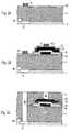
- FIGS. 2A to 2 Eshow cross-sectional views, at different stages of fabrication, of a semiconductor component with an offset memory cell configuration.
- FIG. 1there is shown two known structural concepts for memory cells.
- the method according to the inventioncan be employed in each of the concepts. What is common to both structural concepts is that a switching transistor S 1 , S 2 is formed in a lower plane directly on a semiconductor substrate 1 and a storage capacitor K 1 , K 2 is configured in an upper plane. The two planes are isolated from one another by an intervening insulation layer 4 .
- the switching transistor S 1 and the storage capacitor K 1are essentially configured directly above one another.
- the bottom electrode 31 of the storage capacitor S 1is electrically connected to a drain region 21 of the MOS transistor S 1 (the components of the transistor are also designated by reference numeral 2 ) through the insulation layer 4 via a contact hole 41 (“plug”) filled with a conductive material.
- the switching transistor S 2 and the storage capacitor K 2are configured offset from one another.
- the top electrode 33 of the storage capacitor K 2is electrically connected to the drain region 21 of the MOS transistor S 2 (the components of the transistor are also designated by reference numeral 2 ) through two contact holes.
- the MOS transistor 2 already mentionedis fabricated on a semiconductor substrate 1 as follows: an n- or p-doping is carried out to form the drain region 21 and a source region 23 , between which there is a channel whose conductivity can be controlled by a gate 22 configured above the channel.
- the gate 22may be formed by, or connected to, a word line WL of the memory component.
- the source region 23is connected to a bit line BL of the memory component.
- the MOS transistor 2is subsequently covered with the planarizing insulation layer, for example a first oxide layer 4 .
- a storage capacitor 3is formed on the first oxide layer 4 .
- first of all the contact hole 41is etched into the first oxide layer 4 and filled with a conductive material, for example polycrystalline silicon.
- the bottom electrode 31is then applied above the filled contact hole 41 (possibly isolated from the “plug” by a barrier layer (not illustrated)).
- a dielectric layer 32 of a ferroelectric or paraelectric materialis deposited onto the bottom electrode 31 , for example by metalorganic chemical vapor deposition (MOCVD) or by a sputtering method.
- the dielectric layer 32forms the capacitor dielectric.
- a top electrode 33is deposited over the whole area above the dielectric layer 32 .
- the resulting structureis finally covered with a further planarizing insulation layer 5 , for example likewise including SiO 2 .
- a further contact hole 51is formed in the upper insulation layer 5 , through which hole the top electrode 33 of the storage capacitor 3 can be connected to an external electrical connection p (common capacitor plate) by a suitable conductive material.
- the source region 23 of the MOS transistor 2is connected to the bit line BL as follows: a contact hole 45 extending through both insulation layers 4 and 5 is formed and filled with a conductive material.
- a contact hole 46 comparable to the contact hole 45is formed in order to connect the drain region 21 of the MOS transistor S 2 to the top electrode 33 of the storage capacitor k 2 , 3 by a conductive cross-connection 8 and a further contact hole 52 extending through the upper insulation layer 5 .
- first of all the first oxide layer 4is deposited by customary techniques in the manner already explained with reference to FIG. 1 .
- the oxide layer 4is subsequently planarized by CMP (chemical mechanical polishing).
- the oxide layer 4is coated with a resist mask layer, which is then patterned photolithographically, for example. In this case, care is taken to ensure that a mask structure 6 remains at that location at which the contact hole 46 is to be subsequently formed.
- the low-temperature nitriding step according to the inventionis thereupon carried out.
- the nitriding steptakes place at a substrate temperature of from 50° C. to at most 120° C. and is therefore compatible with the photomask technology used.
- the plasma nitridinghas the effect that nitrogen atoms are incorporated in the first oxide layer 4 outside the mask structure 6 in a region near the surface.
- the nitrided surface region of the first oxide layer 4 thus createdis designated by the reference symbol 7 A.
- the storage capacitor K 2is constructed immediately.
- first of all the bottom Pt electrode 31is applied on the nitrided surface region 7 A of the first oxide layer 4 (See FIG. 2 B).
- the dielectric, in particular paraelectric or ferroelectric, layer 32including, for example, BST or other suitable materials such as e.g. SBTN, PZT, BTO, etc., is then deposited.
- the top Pt electrode 33is deposited onto the dielectric layer 32 and patterned together with the dielectric layer 32 by photolithography and etching technology.
- the dielectric layer 32 and the top Pt electrode 33are preferably deposited and patterned in such a way that both layers extend beyond the bottom electrode 31 at least on one side thereof in the lateral direction and are present in the form of a step on the bottom electrode 31 .
- the step regionenlarges the effective capacitor area.
- This structureis then coated with a thin second oxide layer including e.g. SiO 2 .
- photoresist mask structures 9 . 1 and 9 . 2are produced lithographically on the second oxide layer at suitable locations.
- the mask structure 9 . 2is preferably provided centrally above the storage capacitor K 2 .
- the mask structure 9 . 1covers a region of the second oxide layer which lies directly above the non-nitrided region of the first nitrided oxide layer 7 A.
- the thin second oxide layeris then likewise subjected to plasma nitriding.
- the layeris nitrided in its entire thickness or merely in a region near the surface.
- the nitrided second oxide layer 7 B shown in FIG. 2Bis formed, which continues to include non-nitrided oxide material underneath the photoresist mask structures 9 . 1 and 9 . 2 .
- the planarizing upper insulation layer 5preferably likewise an SiO 2 layer, is then deposited above the structure described (See FIG. 2 C). In this process, which may be carried out with the participation of hydrogen, the capacitor 3 is already protected by the second nitrided oxide layer 7 B.
- both contact holes 46 and 52are etched. Because of the patterning of the nitrided oxide layers 7 A and 7 B which is produced by the masking 6 , 9 . 1 and 9 . 2 , both contact holes 46 and 52 can be formed by customary oxide etching. Etching of different layer materials is not necessary. Consequently, the contact holes 46 and 52 have pronounced dimensionally accurate and planar inner wall surfaces, thereby promoting lateral structural size reduction.
- the contact holes 46 , 52can be formed jointly in a single etching step or else in two individual etching steps.
- a third plasma nitriding stepcan now be carried out.
- near-surface inner wall surface regions 7 C of the two contact holes 46 and 52 and also a surface region of the upper oxide layer 5are nitrided.
- the contact holes 46 and 52are then filled with a suitable conductive material, for example tungsten (W), in the manner already described. Afterward, in a manner not illustrated, a CMP step may be carried out in order to produce a planar surface.
- a suitable conductive materialfor example tungsten (W)
- the PIII methodis usually carried out in an installation including two chambers.
- a continuously burning nitrogen plasma having a high plasma densityis produced in one chamber.
- a magnetic fieldmay be used to control the plasma density.
- the substrate with the oxide layers to be nitridedis situated in the other chamber.
- the two chambersare connected to one another by a perforated screen.
- a voltageis then applied to the substrate for a short time, as a result of which nitrogen ions are extracted from the plasma, accelerated through the perforated screen toward the substrate 1 and stopped in the respectively exposed oxide layer.
- the degree of anisotropy of the nitridingcan be influenced to a great extent by the setting of the plasma and extraction conditions. At a high extraction voltage, anisotropic ion implantation occurs.
- the effect that can be achieved e.g. by decreasing the extraction voltage, increasing the plasma density and also by changing the geometrical ratiosis that the nitriding is brought about by an extended “plasma cloud”. In this case, uniform nitriding of the oxide layers can be achieved even in the case of irregular surface topologies, and it has been shown that contact holes having an aperture ratio of up to about 1:12 can be nitrided to their full length without difficulty.
- the PLAD methodis usually carried out in a single plasma chamber.
- the installationis constructed similarly to a sputtering installation.
- a high-frequency voltageis applied between two electrodes and a nitrogen plasma is ignited.
- the substrateis situated on that electrode toward which the nitrogen ions are accelerated.
- the systemoperates analogously to a sputtering installation that has undergone polarity reversal.
- the degree of anisotropy of the nitridingcan be set as desired by way of the installation geometry and the configuration of the nitrogen plasma.
- Typical nitriding energieslie in the range from 1 to 12 keV.
Landscapes
- Engineering & Computer Science (AREA)
- Physics & Mathematics (AREA)
- Condensed Matter Physics & Semiconductors (AREA)
- General Physics & Mathematics (AREA)
- Manufacturing & Machinery (AREA)
- Computer Hardware Design (AREA)
- Microelectronics & Electronic Packaging (AREA)
- Power Engineering (AREA)
- Semiconductor Memories (AREA)
- Formation Of Insulating Films (AREA)
- Semiconductor Integrated Circuits (AREA)
Abstract
Description
Claims (18)
Applications Claiming Priority (3)
| Application Number | Priority Date | Filing Date | Title |
|---|---|---|---|
| DE10010284.0 | 2000-02-25 | ||
| DE10010284 | 2000-02-25 | ||
| DE10010284ADE10010284C2 (en) | 2000-02-25 | 2000-02-25 | Method for producing a semiconductor component with a capacitor |
Publications (2)
| Publication Number | Publication Date |
|---|---|
| US20010021554A1 US20010021554A1 (en) | 2001-09-13 |
| US6316275B2true US6316275B2 (en) | 2001-11-13 |
Family
ID=7633315
Family Applications (1)
| Application Number | Title | Priority Date | Filing Date |
|---|---|---|---|
| US09/793,351Expired - LifetimeUS6316275B2 (en) | 2000-02-25 | 2001-02-26 | Method for fabricating a semiconductor component |
Country Status (7)
| Country | Link |
|---|---|
| US (1) | US6316275B2 (en) |
| EP (1) | EP1128428B1 (en) |
| JP (1) | JP3990542B2 (en) |
| KR (1) | KR100397881B1 (en) |
| CN (1) | CN1174472C (en) |
| DE (2) | DE10065976A1 (en) |
| TW (1) | TW502399B (en) |
Cited By (8)
| Publication number | Priority date | Publication date | Assignee | Title |
|---|---|---|---|---|
| US20030013263A1 (en)* | 2001-07-11 | 2003-01-16 | Cem Basceri | Capacitor with high dielectric constant materials and method of making |
| US20030089954A1 (en)* | 2001-11-15 | 2003-05-15 | Fujitsu Limited | Semiconductor device and method of manufacturing the same |
| US20050012133A1 (en)* | 2003-05-27 | 2005-01-20 | Matsushita Electric Industrial Co., Ltd | Semiconductor device and method for fabricating the same |
| US20050218443A1 (en)* | 2004-03-26 | 2005-10-06 | Hiroaki Tamura | Ferroelectric memory element and its manufacturing method |
| US20050239251A1 (en)* | 2002-11-13 | 2005-10-27 | Matsushita Electric Industrial Co., Ltd. | Semiconductor device and method for fabricating the same |
| US20050239219A1 (en)* | 2004-04-26 | 2005-10-27 | Moon Bum-Ki | Process for fabrication of a ferrocapacitor with a large effective area |
| US20070018342A1 (en)* | 2005-07-20 | 2007-01-25 | Micron Technology, Inc. | Devices with nanocrystals and methods of formation |
| US20080093658A1 (en)* | 2004-12-28 | 2008-04-24 | Tokyo Electron Limited | Method for Nitriding Tunnel Oxide Film, Method for Manufacturing Non-Volatile Memory Device, Non-Volatile Memory Device, Control Program and Computer-Readable Recording Medium |
Families Citing this family (16)
| Publication number | Priority date | Publication date | Assignee | Title |
|---|---|---|---|---|
| DE10121657B4 (en)* | 2001-05-03 | 2010-02-11 | Qimonda Ag | Microelectronic structure with hydrogen barrier layer |
| US7270573B2 (en)* | 2002-08-30 | 2007-09-18 | Fci Americas Technology, Inc. | Electrical connector with load bearing features |
| JP4636834B2 (en)* | 2002-11-13 | 2011-02-23 | パナソニック株式会社 | Semiconductor device and manufacturing method thereof |
| US7101785B2 (en)* | 2003-07-22 | 2006-09-05 | Infineon Technologies Ag | Formation of a contact in a device, and the device including the contact |
| JP2005229001A (en) | 2004-02-16 | 2005-08-25 | Toshiba Corp | Semiconductor device and manufacturing method of semiconductor device |
| JP4803995B2 (en)* | 2004-06-28 | 2011-10-26 | 富士通セミコンダクター株式会社 | Semiconductor device and manufacturing method thereof |
| JP4042730B2 (en)* | 2004-09-02 | 2008-02-06 | セイコーエプソン株式会社 | Ferroelectric memory and manufacturing method thereof |
| JP2006222389A (en)* | 2005-02-14 | 2006-08-24 | Toshiba Corp | Semiconductor memory device and manufacturing method thereof |
| JP4953580B2 (en)* | 2005-03-03 | 2012-06-13 | 富士通セミコンダクター株式会社 | Manufacturing method of semiconductor device |
| JP2007067066A (en) | 2005-08-30 | 2007-03-15 | Toshiba Corp | Semiconductor device and manufacturing method thereof |
| WO2007060735A1 (en)* | 2005-11-25 | 2007-05-31 | Fujitsu Limited | Semiconductor device and method for manufacturing same |
| JP2006157062A (en)* | 2006-03-10 | 2006-06-15 | Toshiba Corp | Semiconductor device and manufacturing method of semiconductor device |
| JP4567026B2 (en)* | 2007-05-24 | 2010-10-20 | 富士通セミコンダクター株式会社 | Manufacturing method of semiconductor device |
| KR101481574B1 (en)* | 2008-02-13 | 2015-01-14 | 삼성전자주식회사 | Method of manufacturing semiconductor device |
| US10128016B2 (en)* | 2016-01-12 | 2018-11-13 | Asml Netherlands B.V. | EUV element having barrier to hydrogen transport |
| US20230097184A1 (en)* | 2021-09-24 | 2023-03-30 | Intel Corporation | Integrated circuits with high dielectric constant interfacial layering |
Citations (5)
| Publication number | Priority date | Publication date | Assignee | Title |
|---|---|---|---|---|
| US5523595A (en) | 1990-08-21 | 1996-06-04 | Ramtron International Corporation | Semiconductor device having a transistor, a ferroelectric capacitor and a hydrogen barrier film |
| JPH09219498A (en) | 1996-02-13 | 1997-08-19 | Nec Corp | Manufacture of semiconductor device |
| EP0847079A2 (en) | 1996-12-05 | 1998-06-10 | Texas Instruments Incorporated | Method of manufacturing an MIS electrode |
| US6008103A (en) | 1998-02-27 | 1999-12-28 | Siemens Aktiengesellschaft | Method for forming trench capacitors in an integrated circuit |
| US6225656B1 (en)* | 1998-12-01 | 2001-05-01 | Symetrix Corporation | Ferroelectric integrated circuit with protective layer incorporating oxygen and method for fabricating same |
Family Cites Families (3)
| Publication number | Priority date | Publication date | Assignee | Title |
|---|---|---|---|---|
| EP0862203A1 (en)* | 1997-01-31 | 1998-09-02 | Texas Instruments Incorporated | Method for fabricating a semiconductor memory capacitor |
| KR100269314B1 (en)* | 1997-02-17 | 2000-10-16 | 윤종용 | Method for manufacturing a capacitor of a semiconductor device using a plasma processing |
| JP3098474B2 (en)* | 1997-10-31 | 2000-10-16 | 日本電気株式会社 | Method for manufacturing semiconductor device |
- 2000
- 2000-02-25DEDE10065976Apatent/DE10065976A1/ennot_activeCeased
- 2001
- 2001-02-09TWTW090102893Apatent/TW502399B/ennot_activeIP Right Cessation
- 2001-02-22EPEP01104254Apatent/EP1128428B1/ennot_activeExpired - Lifetime
- 2001-02-22DEDE50113179Tpatent/DE50113179D1/ennot_activeExpired - Lifetime
- 2001-02-23CNCNB011049421Apatent/CN1174472C/ennot_activeExpired - Fee Related
- 2001-02-23JPJP2001049279Apatent/JP3990542B2/ennot_activeExpired - Fee Related
- 2001-02-24KRKR10-2001-0009483Apatent/KR100397881B1/ennot_activeExpired - Fee Related
- 2001-02-26USUS09/793,351patent/US6316275B2/ennot_activeExpired - Lifetime
Patent Citations (6)
| Publication number | Priority date | Publication date | Assignee | Title |
|---|---|---|---|---|
| US5523595A (en) | 1990-08-21 | 1996-06-04 | Ramtron International Corporation | Semiconductor device having a transistor, a ferroelectric capacitor and a hydrogen barrier film |
| JPH09219498A (en) | 1996-02-13 | 1997-08-19 | Nec Corp | Manufacture of semiconductor device |
| US6048764A (en) | 1996-02-13 | 2000-04-11 | Nec Corporation | Method for producing semiconductor device with capacitor stacked |
| EP0847079A2 (en) | 1996-12-05 | 1998-06-10 | Texas Instruments Incorporated | Method of manufacturing an MIS electrode |
| US6008103A (en) | 1998-02-27 | 1999-12-28 | Siemens Aktiengesellschaft | Method for forming trench capacitors in an integrated circuit |
| US6225656B1 (en)* | 1998-12-01 | 2001-05-01 | Symetrix Corporation | Ferroelectric integrated circuit with protective layer incorporating oxygen and method for fabricating same |
Cited By (24)
| Publication number | Priority date | Publication date | Assignee | Title |
|---|---|---|---|---|
| US20030013263A1 (en)* | 2001-07-11 | 2003-01-16 | Cem Basceri | Capacitor with high dielectric constant materials and method of making |
| US20060154382A1 (en)* | 2001-07-11 | 2006-07-13 | Cem Basceri | Capacitor with high dielectric constant materials and method of making |
| US20030089954A1 (en)* | 2001-11-15 | 2003-05-15 | Fujitsu Limited | Semiconductor device and method of manufacturing the same |
| US7745232B2 (en) | 2001-11-15 | 2010-06-29 | Fujitsu Semiconductor Limited | Semiconductor device and method of manufacturing the same |
| US20090068764A1 (en)* | 2001-11-15 | 2009-03-12 | Fujitsu Limited | Semiconductor device and method of manufacturing the same |
| US7456454B2 (en) | 2001-11-15 | 2008-11-25 | Fujitsu Limited | Ferroelectric semiconductor device and method of manufacturing the same |
| US7288456B2 (en) | 2002-11-13 | 2007-10-30 | Matsushita Electric Industrial Co., Ltd. | Semiconductor device and method for fabricating the same |
| US7550344B2 (en) | 2002-11-13 | 2009-06-23 | Panasonic Corporation | Semiconductor device and method for fabricating the same |
| US20050239251A1 (en)* | 2002-11-13 | 2005-10-27 | Matsushita Electric Industrial Co., Ltd. | Semiconductor device and method for fabricating the same |
| US20070293007A1 (en)* | 2002-11-13 | 2007-12-20 | Matsushita Electric Industrial Co., Ltd. | Semiconductor device and method for fabricating the same |
| US20060079066A1 (en)* | 2003-05-27 | 2006-04-13 | Matsushita Electric Industrial Co., Ltd. | Semiconductor device and method for fabricating the same |
| US7557011B2 (en) | 2003-05-27 | 2009-07-07 | Panasonic Corporation | Semiconductor device and method for fabricating the same |
| US20050012133A1 (en)* | 2003-05-27 | 2005-01-20 | Matsushita Electric Industrial Co., Ltd | Semiconductor device and method for fabricating the same |
| US7326990B2 (en) | 2003-05-27 | 2008-02-05 | Matsushita Electric Industrial Co., Ltd. | Semiconductor device and method for fabricating the same |
| US7180122B2 (en)* | 2003-05-27 | 2007-02-20 | Matsushita Electric Industrial Co., Ltd. | Semiconductor device and method for fabricating the same |
| US20060220091A1 (en)* | 2003-05-27 | 2006-10-05 | Matsushita Electric Industrial Co., Ltd. | Semiconductor device and method for fabricating the same |
| US20050218443A1 (en)* | 2004-03-26 | 2005-10-06 | Hiroaki Tamura | Ferroelectric memory element and its manufacturing method |
| US20050239219A1 (en)* | 2004-04-26 | 2005-10-27 | Moon Bum-Ki | Process for fabrication of a ferrocapacitor with a large effective area |
| US20080093658A1 (en)* | 2004-12-28 | 2008-04-24 | Tokyo Electron Limited | Method for Nitriding Tunnel Oxide Film, Method for Manufacturing Non-Volatile Memory Device, Non-Volatile Memory Device, Control Program and Computer-Readable Recording Medium |
| US20070018342A1 (en)* | 2005-07-20 | 2007-01-25 | Micron Technology, Inc. | Devices with nanocrystals and methods of formation |
| US7927948B2 (en) | 2005-07-20 | 2011-04-19 | Micron Technology, Inc. | Devices with nanocrystals and methods of formation |
| US8288818B2 (en) | 2005-07-20 | 2012-10-16 | Micron Technology, Inc. | Devices with nanocrystals and methods of formation |
| US8501563B2 (en) | 2005-07-20 | 2013-08-06 | Micron Technology, Inc. | Devices with nanocrystals and methods of formation |
| US8921914B2 (en) | 2005-07-20 | 2014-12-30 | Micron Technology, Inc. | Devices with nanocrystals and methods of formation |
Also Published As
| Publication number | Publication date |
|---|---|
| JP2001291843A (en) | 2001-10-19 |
| KR100397881B1 (en) | 2003-09-13 |
| KR20010085573A (en) | 2001-09-07 |
| JP3990542B2 (en) | 2007-10-17 |
| EP1128428A3 (en) | 2004-10-27 |
| DE10065976A1 (en) | 2002-02-21 |
| EP1128428A2 (en) | 2001-08-29 |
| EP1128428B1 (en) | 2007-10-31 |
| TW502399B (en) | 2002-09-11 |
| US20010021554A1 (en) | 2001-09-13 |
| CN1174472C (en) | 2004-11-03 |
| CN1310468A (en) | 2001-08-29 |
| DE50113179D1 (en) | 2007-12-13 |
Similar Documents
| Publication | Publication Date | Title |
|---|---|---|
| US6316275B2 (en) | Method for fabricating a semiconductor component | |
| US5478772A (en) | Method for forming a storage cell capacitor compatible with high dielectric constant materials | |
| US5834357A (en) | Fabricating method of making a fin shaped capacitor | |
| US6338994B1 (en) | Semiconductor device and method of fabricating thereof | |
| US7253052B2 (en) | Method for forming a storage cell capacitor compatible with high dielectric constant materials | |
| US20030062558A1 (en) | Memory cell capacitor structure and method of formation | |
| US20010026988A1 (en) | Method of manufacturing semiconductor devices utilizing underlayer-dependency of deposition of capacitor electrode film, and semiconductor device | |
| US6432767B2 (en) | Method of fabricating semiconductor device | |
| US7015532B2 (en) | Capacitor compatible with high dielectric constant materials having a low contact resistance layer and the method for forming same | |
| KR19980066285A (en) | Contact wiring method of semiconductor device and capacitor manufacturing method using same | |
| KR20030035815A (en) | Capacitor, method for fabricating the capacitor, and method for fabricating semiconductor device | |
| US6503792B2 (en) | Method for fabricating a patterned metal-oxide-containing layer | |
| US6812042B2 (en) | Capacitor and method for fabricating ferroelectric memory device with the same | |
| US20020061604A1 (en) | Method for fabricating a ferroelectric or paraelectric metal oxide-containing layer and a memory component therefrom | |
| US7157371B2 (en) | Barrier layer and a method for suppressing diffusion processes during the production of semiconductor devices | |
| KR100424710B1 (en) | Fabricating method of semiconductor device | |
| KR100519514B1 (en) | Method of forming capacitor provied with TaON dielectric layer | |
| KR100432986B1 (en) | Method for producing specific local openings in a layer | |
| KR100633330B1 (en) | Capacitor Manufacturing Method of Semiconductor Device | |
| KR100338822B1 (en) | Method of forming storage node electorde in semiconductor device | |
| US6891211B2 (en) | Ferroelectric random access memory device and method for fabricating the same | |
| KR100476380B1 (en) | Method for fabricating cylindrical capacitor in semiconductor device | |
| KR100846368B1 (en) | Memory device and manufacturing method thereof | |
| KR100636661B1 (en) | High reliability capacitor manufacturing method | |
| KR20010008584A (en) | Method of forming capacitor in high integrated semiconductor device |
Legal Events
| Date | Code | Title | Description |
|---|---|---|---|
| AS | Assignment | Owner name:INFINEON TECHNOLOGIES AG, GERMANY Free format text:ASSIGNMENT OF ASSIGNORS INTEREST;ASSIGNOR:HOPFNER, JOACHIM;REEL/FRAME:012190/0623 Effective date:20010314 | |
| STCF | Information on status: patent grant | Free format text:PATENTED CASE | |
| FPAY | Fee payment | Year of fee payment:4 | |
| FPAY | Fee payment | Year of fee payment:8 | |
| AS | Assignment | Owner name:QIMONDA AG, GERMANY Free format text:ASSIGNMENT OF ASSIGNORS INTEREST;ASSIGNOR:INFINEON TECHNOLOGIES AG;REEL/FRAME:023828/0001 Effective date:20060425 | |
| FPAY | Fee payment | Year of fee payment:12 | |
| AS | Assignment | Owner name:INFINEON TECHNOLOGIES AG, GERMANY Free format text:ASSIGNMENT OF ASSIGNORS INTEREST;ASSIGNOR:QIMONDA AG;REEL/FRAME:035623/0001 Effective date:20141009 | |
| AS | Assignment | Owner name:POLARIS INNOVATIONS LIMITED, IRELAND Free format text:ASSIGNMENT OF ASSIGNORS INTEREST;ASSIGNOR:INFINEON TECHNOLOGIES AG;REEL/FRAME:036539/0196 Effective date:20150708 |