US6316162B1 - Polymer and a forming method of a micro pattern using the same - Google Patents
Polymer and a forming method of a micro pattern using the sameDownload PDFInfo
- Publication number
- US6316162B1 US6316162B1US09/301,945US30194599AUS6316162B1US 6316162 B1US6316162 B1US 6316162B1US 30194599 AUS30194599 AUS 30194599AUS 6316162 B1US6316162 B1US 6316162B1
- Authority
- US
- United States
- Prior art keywords
- photoresist
- pattern
- carboxylate
- forming
- polymer
- Prior art date
- Legal status (The legal status is an assumption and is not a legal conclusion. Google has not performed a legal analysis and makes no representation as to the accuracy of the status listed.)
- Expired - Fee Related
Links
- 238000000034methodMethods0.000titleclaimsabstractdescription50
- 229920000642polymerPolymers0.000titleabstractdescription44
- 229920002120photoresistant polymerPolymers0.000claimsabstractdescription99
- 125000000075primary alcohol groupChemical group0.000claimsabstractdescription4
- 125000003198secondary alcohol groupChemical group0.000claimsabstractdescription4
- 238000006884silylation reactionMethods0.000claimsdescription28
- 238000006243chemical reactionMethods0.000claimsdescription16
- -1tetramethyldisiazaneChemical compound0.000claimsdescription14
- FFUAGWLWBBFQJT-UHFFFAOYSA-NhexamethyldisilazaneChemical compoundC[Si](C)(C)N[Si](C)(C)CFFUAGWLWBBFQJT-UHFFFAOYSA-N0.000claimsdescription13
- 238000005530etchingMethods0.000claimsdescription11
- 239000003795chemical substances by applicationSubstances0.000claimsdescription10
- 238000006116polymerization reactionMethods0.000claimsdescription8
- 125000002843carboxylic acid groupChemical group0.000claimsdescription5
- 239000000178monomerSubstances0.000claimsdescription4
- KZFNONVXCZVHRD-UHFFFAOYSA-Ndimethylamino(dimethyl)siliconChemical compoundCN(C)[Si](C)CKZFNONVXCZVHRD-UHFFFAOYSA-N0.000claimsdescription3
- JOOMLFKONHCLCJ-UHFFFAOYSA-NN-(trimethylsilyl)diethylamineChemical compoundCCN(CC)[Si](C)(C)CJOOMLFKONHCLCJ-UHFFFAOYSA-N0.000claimsdescription2
- 239000011248coating agentSubstances0.000claimsdescription2
- 238000000576coating methodMethods0.000claimsdescription2
- 238000001312dry etchingMethods0.000claimsdescription2
- KAHVZNKZQFSBFW-UHFFFAOYSA-Nn-methyl-n-trimethylsilylmethanamineChemical compoundCN(C)[Si](C)(C)CKAHVZNKZQFSBFW-UHFFFAOYSA-N0.000claimsdescription2
- 239000000758substrateSubstances0.000claims2
- JMBUOHCQHAPBFY-UHFFFAOYSA-NCN(C)C[SiH3]Chemical compoundCN(C)C[SiH3]JMBUOHCQHAPBFY-UHFFFAOYSA-N0.000claims1
- 230000001678irradiating effectEffects0.000claims1
- 239000003960organic solventSubstances0.000claims1
- 238000005507sprayingMethods0.000claims1
- 239000004065semiconductorSubstances0.000abstractdescription9
- 238000010884ion-beam techniqueMethods0.000abstractdescription3
- WYURNTSHIVDZCO-UHFFFAOYSA-NTetrahydrofuranChemical compoundC1CCOC1WYURNTSHIVDZCO-UHFFFAOYSA-N0.000description34
- FPYJFEHAWHCUMM-UHFFFAOYSA-Nmaleic anhydrideChemical compoundO=C1OC(=O)C=C1FPYJFEHAWHCUMM-UHFFFAOYSA-N0.000description27
- OZAIFHULBGXAKX-UHFFFAOYSA-N2,2'-azo-bis-isobutyronitrileSubstancesN#CC(C)(C)N=NC(C)(C)C#NOZAIFHULBGXAKX-UHFFFAOYSA-N0.000description26
- 238000002360preparation methodMethods0.000description26
- YLQBMQCUIZJEEH-UHFFFAOYSA-NtetrahydrofuranNatural productsC=1C=COC=1YLQBMQCUIZJEEH-UHFFFAOYSA-N0.000description17
- 239000010410layerSubstances0.000description16
- 239000002904solventSubstances0.000description15
- RTZKZFJDLAIYFH-UHFFFAOYSA-NDiethyl etherChemical compoundCCOCCRTZKZFJDLAIYFH-UHFFFAOYSA-N0.000description14
- BZBMBZJUNPMEBD-UHFFFAOYSA-Ntert-butyl bicyclo[2.2.1]hept-2-ene-5-carboxylateChemical compoundC1C2C(C(=O)OC(C)(C)C)CC1C=C2BZBMBZJUNPMEBD-UHFFFAOYSA-N0.000description13
- PFDKMHNKWZYRPM-UHFFFAOYSA-Ntert-butyl bicyclo[2.2.2]oct-2-ene-5-carboxylateChemical compoundC1CC2C(C(=O)OC(C)(C)C)CC1C=C2PFDKMHNKWZYRPM-UHFFFAOYSA-N0.000description12
- PHSXOZKMZYKHLY-UHFFFAOYSA-N2-hydroxyethyl bicyclo[2.2.1]hept-2-ene-5-carboxylateChemical compoundC1C2C(C(=O)OCCO)CC1C=C2PHSXOZKMZYKHLY-UHFFFAOYSA-N0.000description9
- MYBZOQDIRORKOI-UHFFFAOYSA-N3-hydroxypropyl bicyclo[2.2.1]hept-2-ene-5-carboxylateChemical compoundC1C2C(C(=O)OCCCO)CC1C=C2MYBZOQDIRORKOI-UHFFFAOYSA-N0.000description9
- OZAIFHULBGXAKX-VAWYXSNFSA-NAIBNSubstancesN#CC(C)(C)\N=N\C(C)(C)C#NOZAIFHULBGXAKX-VAWYXSNFSA-N0.000description9
- 230000015572biosynthetic processEffects0.000description9
- 150000001875compoundsChemical class0.000description8
- 239000002244precipitateSubstances0.000description8
- 239000000047productSubstances0.000description8
- 238000003786synthesis reactionMethods0.000description8
- 0*C(=O)C1CC2CC1C(C)C2C1C2CC(CC2C(=O)C(C)(C)C)C1C1C(=O)OC(=O)C1CChemical compound*C(=O)C1CC2CC1C(C)C2C1C2CC(CC2C(=O)C(C)(C)C)C1C1C(=O)OC(=O)C1C0.000description7
- VYPSYNLAJGMNEJ-UHFFFAOYSA-NSilicium dioxideChemical compoundO=[Si]=OVYPSYNLAJGMNEJ-UHFFFAOYSA-N0.000description7
- 239000012299nitrogen atmosphereSubstances0.000description7
- 229910052814silicon oxideInorganic materials0.000description7
- AQTMPYCVJDXCIR-UHFFFAOYSA-N2-hydroxyethyl bicyclo[2.2.2]oct-2-ene-5-carboxylateChemical compoundC1CC2C(C(=O)OCCO)CC1C=C2AQTMPYCVJDXCIR-UHFFFAOYSA-N0.000description6
- FIAUVBFWUHSYMM-UHFFFAOYSA-N3-hydroxypropyl bicyclo[2.2.2]oct-2-ene-5-carboxylateChemical compoundC1CC2C(C(=O)OCCCO)CC1C=C2FIAUVBFWUHSYMM-UHFFFAOYSA-N0.000description6
- 238000000655nuclear magnetic resonance spectrumMethods0.000description6
- IJGRMHOSHXDMSA-UHFFFAOYSA-NAtomic nitrogenChemical compoundN#NIJGRMHOSHXDMSA-UHFFFAOYSA-N0.000description4
- VQTUBCCKSQIDNK-UHFFFAOYSA-NIsobuteneChemical compoundCC(C)=CVQTUBCCKSQIDNK-UHFFFAOYSA-N0.000description4
- 229920005989resinPolymers0.000description4
- 239000011347resinSubstances0.000description4
- ZWEHNKRNPOVVGH-UHFFFAOYSA-N2-ButanoneChemical compoundCCC(C)=OZWEHNKRNPOVVGH-UHFFFAOYSA-N0.000description3
- UHOVQNZJYSORNB-UHFFFAOYSA-NBenzeneChemical compoundC1=CC=CC=C1UHOVQNZJYSORNB-UHFFFAOYSA-N0.000description3
- OKKJLVBELUTLKV-UHFFFAOYSA-NMethanolChemical groupOCOKKJLVBELUTLKV-UHFFFAOYSA-N0.000description3
- ZMXDDKWLCZADIW-UHFFFAOYSA-NN,N-DimethylformamideChemical compoundCN(C)C=OZMXDDKWLCZADIW-UHFFFAOYSA-N0.000description3
- XUIMIQQOPSSXEZ-UHFFFAOYSA-NSiliconChemical group[Si]XUIMIQQOPSSXEZ-UHFFFAOYSA-N0.000description3
- YXFVVABEGXRONW-UHFFFAOYSA-NTolueneChemical compoundCC1=CC=CC=C1YXFVVABEGXRONW-UHFFFAOYSA-N0.000description3
- 238000004519manufacturing processMethods0.000description3
- VLKZOEOYAKHREP-UHFFFAOYSA-Nn-HexaneChemical compoundCCCCCCVLKZOEOYAKHREP-UHFFFAOYSA-N0.000description3
- 229910052757nitrogenInorganic materials0.000description3
- 125000000999tert-butyl groupChemical group[H]C([H])([H])C(*)(C([H])([H])[H])C([H])([H])[H]0.000description3
- 1250000009542-hydroxyethyl groupChemical group[H]C([*])([H])C([H])([H])O[H]0.000description2
- LFQSCWFLJHTTHZ-UHFFFAOYSA-NEthanolChemical groupCCOLFQSCWFLJHTTHZ-UHFFFAOYSA-N0.000description2
- LRHPLDYGYMQRHN-UHFFFAOYSA-NN-ButanolChemical groupCCCCOLRHPLDYGYMQRHN-UHFFFAOYSA-N0.000description2
- 229910014299N-SiInorganic materials0.000description2
- GJWAPAVRQYYSTK-UHFFFAOYSA-N[(dimethyl-$l^{3}-silanyl)amino]-dimethylsiliconChemical compoundC[Si](C)N[Si](C)CGJWAPAVRQYYSTK-UHFFFAOYSA-N0.000description2
- 239000002253acidSubstances0.000description2
- VBQBQIPNKHQYAF-UHFFFAOYSA-Nbutyl bicyclo[2.2.1]hept-2-ene-5-carboxylate;furan-2,5-dioneChemical compoundO=C1OC(=O)C=C1.C1C2C(C(=O)OCCCC)CC1C=C2VBQBQIPNKHQYAF-UHFFFAOYSA-N0.000description2
- ZQMIGQNCOMNODD-UHFFFAOYSA-Ndiacetyl peroxideChemical compoundCC(=O)OOC(C)=OZQMIGQNCOMNODD-UHFFFAOYSA-N0.000description2
- BHXIWUJLHYHGSJ-UHFFFAOYSA-Nethyl 3-ethoxypropanoateChemical compoundCCOCCC(=O)OCCBHXIWUJLHYHGSJ-UHFFFAOYSA-N0.000description2
- 239000003505polymerization initiatorSubstances0.000description2
- BDERNNFJNOPAEC-UHFFFAOYSA-Npropan-1-olChemical groupCCCOBDERNNFJNOPAEC-UHFFFAOYSA-N0.000description2
- 229910052710siliconInorganic materials0.000description2
- FAYMLNNRGCYLSR-UHFFFAOYSA-Mtriphenylsulfonium triflateChemical compound[O-]S(=O)(=O)C(F)(F)F.C1=CC=CC=C1[S+](C=1C=CC=CC=1)C1=CC=CC=C1FAYMLNNRGCYLSR-UHFFFAOYSA-M0.000description2
- RYHBNJHYFVUHQT-UHFFFAOYSA-N1,4-DioxaneChemical compoundC1COCCO1RYHBNJHYFVUHQT-UHFFFAOYSA-N0.000description1
- LGJCFVYMIJLQJO-UHFFFAOYSA-N1-dodecylperoxydodecaneChemical compoundCCCCCCCCCCCCOOCCCCCCCCCCCCLGJCFVYMIJLQJO-UHFFFAOYSA-N0.000description1
- VUBUXALTYMBEQO-UHFFFAOYSA-N2,2,3,3,3-pentafluoro-1-phenylpropan-1-oneChemical compoundFC(F)(F)C(F)(F)C(=O)C1=CC=CC=C1VUBUXALTYMBEQO-UHFFFAOYSA-N0.000description1
- 239000004342Benzoyl peroxideSubstances0.000description1
- OMPJBNCRMGITSC-UHFFFAOYSA-NBenzoylperoxideChemical compoundC=1C=CC=CC=1C(=O)OOC(=O)C1=CC=CC=C1OMPJBNCRMGITSC-UHFFFAOYSA-N0.000description1
- XCZSBCXFDCJQPX-UHFFFAOYSA-NC12C(CC(C=C1)CC2)C(=O)OCCCC.C2(C=C/C(=O)O2)=OChemical compoundC12C(CC(C=C1)CC2)C(=O)OCCCC.C2(C=C/C(=O)O2)=OXCZSBCXFDCJQPX-UHFFFAOYSA-N0.000description1
- WTBUHEYPAAYRAN-UHFFFAOYSA-NCC(C)(C)C(=O)C1CC2C=CC1C2Chemical compoundCC(C)(C)C(=O)C1CC2C=CC1C2WTBUHEYPAAYRAN-UHFFFAOYSA-N0.000description1
- COPHRUNGFZHJBZ-UHFFFAOYSA-NCC1C(=O)OC(=O)C1C1C2CC(C(=O)C(C)(C)C)C(C2)C1C1C2CC(C(=O)CCCO)C(C2)C1CChemical compoundCC1C(=O)OC(=O)C1C1C2CC(C(=O)C(C)(C)C)C(C2)C1C1C2CC(C(=O)CCCO)C(C2)C1CCOPHRUNGFZHJBZ-UHFFFAOYSA-N0.000description1
- OUZUBEGCQRDTQH-UHFFFAOYSA-NCC1C(=O)OC(=O)C1C1C2CC(C(=O)C(C)(C)C)C(C2)C1C1C2CC(C(=O)CCO)C(C2)C1CChemical compoundCC1C(=O)OC(=O)C1C1C2CC(C(=O)C(C)(C)C)C(C2)C1C1C2CC(C(=O)CCO)C(C2)C1COUZUBEGCQRDTQH-UHFFFAOYSA-N0.000description1
- NBWNBQBALFTFRR-UHFFFAOYSA-NCC1C(=O)OC(=O)C1C1C2CC(C(=O)C(C)(C)C)C(C2)C1C1C2CCC(C(C(=O)CCCO)C2)C1CChemical compoundCC1C(=O)OC(=O)C1C1C2CC(C(=O)C(C)(C)C)C(C2)C1C1C2CCC(C(C(=O)CCCO)C2)C1CNBWNBQBALFTFRR-UHFFFAOYSA-N0.000description1
- FXPKOXDPUFCPPW-UHFFFAOYSA-NCC1C(=O)OC(=O)C1C1C2CC(C(=O)C(C)(C)C)C(C2)C1CC1(C)CC2CCC1C(C(=O)CCO)C2Chemical compoundCC1C(=O)OC(=O)C1C1C2CC(C(=O)C(C)(C)C)C(C2)C1CC1(C)CC2CCC1C(C(=O)CCO)C2FXPKOXDPUFCPPW-UHFFFAOYSA-N0.000description1
- LDRDMIYUZZRONW-UHFFFAOYSA-NCC1C(=O)OC(=O)C1C1C2CCC(C(C(=O)C(C)(C)C)C2)C1C1C2CC(C(=O)CCO)C(C2)C1CChemical compoundCC1C(=O)OC(=O)C1C1C2CCC(C(C(=O)C(C)(C)C)C2)C1C1C2CC(C(=O)CCO)C(C2)C1CLDRDMIYUZZRONW-UHFFFAOYSA-N0.000description1
- UXVQLULAHRBZOG-UHFFFAOYSA-NCC1C(=O)OC(=O)C1C1C2CCC(C(C(=O)C(C)(C)C)C2)C1C1C2CCC(C(C(=O)CCCO)C2)C1CChemical compoundCC1C(=O)OC(=O)C1C1C2CCC(C(C(=O)C(C)(C)C)C2)C1C1C2CCC(C(C(=O)CCCO)C2)C1CUXVQLULAHRBZOG-UHFFFAOYSA-N0.000description1
- DSGKRGLWHPUSKQ-UHFFFAOYSA-NCC1C(=O)OC(=O)C1C1C2CCC(C(C(=O)C(C)(C)C)C2)C1C1C2CCC(C(C(=O)CCO)C2)C1CChemical compoundCC1C(=O)OC(=O)C1C1C2CCC(C(C(=O)C(C)(C)C)C2)C1C1C2CCC(C(C(=O)CCO)C2)C1CDSGKRGLWHPUSKQ-UHFFFAOYSA-N0.000description1
- QYLBEMPGQAUENX-UHFFFAOYSA-NCC1C(=O)OC(=O)C1CC1(C2C3CC(C(=O)CCCO)C(C3)C2C)CC2CCC1C(C(=O)C(C)(C)C)C2Chemical compoundCC1C(=O)OC(=O)C1CC1(C2C3CC(C(=O)CCCO)C(C3)C2C)CC2CCC1C(C(=O)C(C)(C)C)C2QYLBEMPGQAUENX-UHFFFAOYSA-N0.000description1
- 229920000089Cyclic olefin copolymerPolymers0.000description1
- XDTMQSROBMDMFD-UHFFFAOYSA-NCyclohexaneChemical compoundC1CCCCC1XDTMQSROBMDMFD-UHFFFAOYSA-N0.000description1
- AMQJEAYHLZJPGS-UHFFFAOYSA-NN-PentanolChemical groupCCCCCOAMQJEAYHLZJPGS-UHFFFAOYSA-N0.000description1
- 229910003849O-SiInorganic materials0.000description1
- 229910003872O—SiInorganic materials0.000description1
- 229920001665Poly-4-vinylphenolPolymers0.000description1
- 229910018557Si OInorganic materials0.000description1
- NINIDFKCEFEMDL-UHFFFAOYSA-NSulfurChemical group[S]NINIDFKCEFEMDL-UHFFFAOYSA-N0.000description1
- 150000007513acidsChemical class0.000description1
- 125000003158alcohol groupChemical group0.000description1
- 150000001412aminesChemical class0.000description1
- 239000012300argon atmosphereSubstances0.000description1
- 235000019400benzoyl peroxideNutrition0.000description1
- RZQRFJYKWMUYLB-UHFFFAOYSA-Nbicyclo[2.2.2]oct-2-ene-5-carboxylic acidChemical compoundC1CC2C(C(=O)O)CC1C=C2RZQRFJYKWMUYLB-UHFFFAOYSA-N0.000description1
- 238000012662bulk polymerizationMethods0.000description1
- 239000006227byproductSubstances0.000description1
- 230000007812deficiencyEffects0.000description1
- LSXWFXONGKSEMY-UHFFFAOYSA-Ndi-tert-butyl peroxideChemical compoundCC(C)(C)OOC(C)(C)CLSXWFXONGKSEMY-UHFFFAOYSA-N0.000description1
- 238000009792diffusion processMethods0.000description1
- 235000019441ethanolNutrition0.000description1
- 238000010528free radical solution polymerization reactionMethods0.000description1
- 239000007789gasSubstances0.000description1
- 125000002887hydroxy groupChemical group[H]O*0.000description1
- 230000010354integrationEffects0.000description1
- BDJSOPWXYLFTNW-UHFFFAOYSA-Nmethyl 3-methoxypropanoateChemical compoundCOCCC(=O)OCBDJSOPWXYLFTNW-UHFFFAOYSA-N0.000description1
- 238000002156mixingMethods0.000description1
- 238000012986modificationMethods0.000description1
- 230000004048modificationEffects0.000description1
- 125000004433nitrogen atomChemical groupN*0.000description1
- 229920003986novolacPolymers0.000description1
- 239000012466permeateSubstances0.000description1
- 239000005011phenolic resinSubstances0.000description1
- 230000000379polymerizing effectEffects0.000description1
- LLHKCFNBLRBOGN-UHFFFAOYSA-Npropylene glycol methyl ether acetateChemical compoundCOCC(C)OC(C)=OLLHKCFNBLRBOGN-UHFFFAOYSA-N0.000description1
- 230000005855radiationEffects0.000description1
- 150000003839saltsChemical class0.000description1
- 238000001878scanning electron micrographMethods0.000description1
- 230000035945sensitivityEffects0.000description1
- 239000010703siliconSubstances0.000description1
- LIVNPJMFVYWSIS-UHFFFAOYSA-Nsilicon monoxideInorganic materials[Si-]#[O+]LIVNPJMFVYWSIS-UHFFFAOYSA-N0.000description1
- 239000002356single layerSubstances0.000description1
- LXAWHMFHGHNIHC-UHFFFAOYSA-Nsulfanyl trifluoromethanesulfonateChemical compoundFC(F)(F)S(=O)(=O)OSLXAWHMFHGHNIHC-UHFFFAOYSA-N0.000description1
- 125000001650tertiary alcohol groupChemical group0.000description1
Images


Classifications
- C—CHEMISTRY; METALLURGY
- C08—ORGANIC MACROMOLECULAR COMPOUNDS; THEIR PREPARATION OR CHEMICAL WORKING-UP; COMPOSITIONS BASED THEREON
- C08F—MACROMOLECULAR COMPOUNDS OBTAINED BY REACTIONS ONLY INVOLVING CARBON-TO-CARBON UNSATURATED BONDS
- C08F8/00—Chemical modification by after-treatment
- C08F8/42—Introducing metal atoms or metal-containing groups
- C—CHEMISTRY; METALLURGY
- C08—ORGANIC MACROMOLECULAR COMPOUNDS; THEIR PREPARATION OR CHEMICAL WORKING-UP; COMPOSITIONS BASED THEREON
- C08F—MACROMOLECULAR COMPOUNDS OBTAINED BY REACTIONS ONLY INVOLVING CARBON-TO-CARBON UNSATURATED BONDS
- C08F222/00—Copolymers of compounds having one or more unsaturated aliphatic radicals, each having only one carbon-to-carbon double bond, and at least one being terminated by a carboxyl radical and containing at least one other carboxyl radical in the molecule; Salts, anhydrides, esters, amides, imides, or nitriles thereof
- C08F222/04—Anhydrides, e.g. cyclic anhydrides
- C08F222/06—Maleic anhydride
- C—CHEMISTRY; METALLURGY
- C08—ORGANIC MACROMOLECULAR COMPOUNDS; THEIR PREPARATION OR CHEMICAL WORKING-UP; COMPOSITIONS BASED THEREON
- C08F—MACROMOLECULAR COMPOUNDS OBTAINED BY REACTIONS ONLY INVOLVING CARBON-TO-CARBON UNSATURATED BONDS
- C08F232/00—Copolymers of cyclic compounds containing no unsaturated aliphatic radicals in a side chain, and having one or more carbon-to-carbon double bonds in a carbocyclic ring system
- C08F232/02—Copolymers of cyclic compounds containing no unsaturated aliphatic radicals in a side chain, and having one or more carbon-to-carbon double bonds in a carbocyclic ring system having no condensed rings
- C08F232/04—Copolymers of cyclic compounds containing no unsaturated aliphatic radicals in a side chain, and having one or more carbon-to-carbon double bonds in a carbocyclic ring system having no condensed rings having one carbon-to-carbon double bond
- G—PHYSICS
- G03—PHOTOGRAPHY; CINEMATOGRAPHY; ANALOGOUS TECHNIQUES USING WAVES OTHER THAN OPTICAL WAVES; ELECTROGRAPHY; HOLOGRAPHY
- G03F—PHOTOMECHANICAL PRODUCTION OF TEXTURED OR PATTERNED SURFACES, e.g. FOR PRINTING, FOR PROCESSING OF SEMICONDUCTOR DEVICES; MATERIALS THEREFOR; ORIGINALS THEREFOR; APPARATUS SPECIALLY ADAPTED THEREFOR
- G03F7/00—Photomechanical, e.g. photolithographic, production of textured or patterned surfaces, e.g. printing surfaces; Materials therefor, e.g. comprising photoresists; Apparatus specially adapted therefor
- G03F7/004—Photosensitive materials
- G03F7/0045—Photosensitive materials with organic non-macromolecular light-sensitive compounds not otherwise provided for, e.g. dissolution inhibitors
- G—PHYSICS
- G03—PHOTOGRAPHY; CINEMATOGRAPHY; ANALOGOUS TECHNIQUES USING WAVES OTHER THAN OPTICAL WAVES; ELECTROGRAPHY; HOLOGRAPHY
- G03F—PHOTOMECHANICAL PRODUCTION OF TEXTURED OR PATTERNED SURFACES, e.g. FOR PRINTING, FOR PROCESSING OF SEMICONDUCTOR DEVICES; MATERIALS THEREFOR; ORIGINALS THEREFOR; APPARATUS SPECIALLY ADAPTED THEREFOR
- G03F7/00—Photomechanical, e.g. photolithographic, production of textured or patterned surfaces, e.g. printing surfaces; Materials therefor, e.g. comprising photoresists; Apparatus specially adapted therefor
- G03F7/004—Photosensitive materials
- G03F7/039—Macromolecular compounds which are photodegradable, e.g. positive electron resists
- G—PHYSICS
- G03—PHOTOGRAPHY; CINEMATOGRAPHY; ANALOGOUS TECHNIQUES USING WAVES OTHER THAN OPTICAL WAVES; ELECTROGRAPHY; HOLOGRAPHY
- G03F—PHOTOMECHANICAL PRODUCTION OF TEXTURED OR PATTERNED SURFACES, e.g. FOR PRINTING, FOR PROCESSING OF SEMICONDUCTOR DEVICES; MATERIALS THEREFOR; ORIGINALS THEREFOR; APPARATUS SPECIALLY ADAPTED THEREFOR
- G03F7/00—Photomechanical, e.g. photolithographic, production of textured or patterned surfaces, e.g. printing surfaces; Materials therefor, e.g. comprising photoresists; Apparatus specially adapted therefor
- G03F7/26—Processing photosensitive materials; Apparatus therefor
- G03F7/38—Treatment before imagewise removal, e.g. prebaking
- Y—GENERAL TAGGING OF NEW TECHNOLOGICAL DEVELOPMENTS; GENERAL TAGGING OF CROSS-SECTIONAL TECHNOLOGIES SPANNING OVER SEVERAL SECTIONS OF THE IPC; TECHNICAL SUBJECTS COVERED BY FORMER USPC CROSS-REFERENCE ART COLLECTIONS [XRACs] AND DIGESTS
- Y10—TECHNICAL SUBJECTS COVERED BY FORMER USPC
- Y10S—TECHNICAL SUBJECTS COVERED BY FORMER USPC CROSS-REFERENCE ART COLLECTIONS [XRACs] AND DIGESTS
- Y10S430/00—Radiation imagery chemistry: process, composition, or product thereof
- Y10S430/1053—Imaging affecting physical property or radiation sensitive material, or producing nonplanar or printing surface - process, composition, or product: radiation sensitive composition or product or process of making binder containing
- Y10S430/1055—Radiation sensitive composition or product or process of making
- Y10S430/106—Binder containing
Definitions
- the present inventionrelates to a polymer useful as a photoresist in a lithographic process for fabricating a semiconductor device, and a method of forming a micro pattern using the same. More specifically, the present invention relates to a polymer which can be used in a photoresist composition for forming an ultra-micro pattern in the manufacture of 4G and 16G DRAM semiconductor chips using short wavelength light sources, such as KrF (248 mn), ArF (193 nm), an E-beam, or an ion-beam.
- the polymer of the present inventionis particularity useful in a photoresist composition for the top surface image (TSI) process using silylation.
- a photoresistis generally used to form a pattern with a fixed form on a semiconductor element.
- a photoresist solutionis coated on a surface of a semiconductor wafer, the coated photoresist is exposed to patterned light, and then the wafer undergoes a developing process. As a result, a photoresist pattern is formed on the wafer.
- the photoresist patternis manufactured using a conventional silylation process
- the photoresistis usually composed of diazonaphtoquinones compounds and a novolac resin, or a photo acid generator and polyvinyl phenol resin.
- the photoresist resinis exposed to the patterned light source (e.g. ArF, KrF, or I line) and then baked, an alcohol group (R—O—H) is formed in the resin at the exposed regions.
- the photoresist resinis silylated with a silylation agent such as hexamethyl disilazane or tetramethyl disilazane.
- an N—Si bondis first formed, but since the N—Si bond is weak, it then reacts with the R—O—H group in the photoresist polymer to form a R—O—Si bond.
- the photoresist resin with bonded silicon atomsthen undergoes a dry developing using O 2 plasma to form a silicon oxide film. The lower portions of the silicon oxide film remain even after the development of the photoresist and as a result, the desired pattern is formed.
- the above-described silylation process for forming a photoresist patternhas several deficiencies when it is used with shorter wavelength radiation.
- a KrF eximer laseris used as the light source to expose known photoresist polymers
- the lens of the exposercan be damaged due to the high energy level of the ArF light. Therefore, the photoresist must be exposed to a lower amount of energy, for example, less than 10 mJ/cm 2 . If the photoresist is not exposed sufficiently to this lower energy, the desired pattern is not formed.
- the unique photoresist polymers of the present inventionsolve the above-described problems of the prior art.
- the heat-resistant character of the polymers of this inventionallow the high temperatures required by the post-exposure baking and silylation steps of the TSI process to be obtained.
- the polymers of the present inventionare particularity suited for use in chemically amplied photoresists wherein a photoresist pattern can be resolved even using a small amount of energy (e.g., 10 mJ/cm 2 ), thereby preventing the damage to the lens of the exposer and the photoresist pattern collapse or insufficient resolution which occurs in the prior art during the formation of the micro pattern using an ArF (193 nm) light source.
- the polymers of the present inventionare advantageously used in the silylation process wherein a chemically amplified photoresist and O 2 plasma are used to form a silicon oxide film which increases the etching and heat resistance of the photoresist such that an acceptable micro pattern can be formed using the dry developing process.
- the present inventionrelates to a polymer which is suitable for use as a single layer photoresist, and preferably as a photoresist in the TSI process.
- Preferred photoresist polymers of the present inventionare represented by the following Formula 1:
- Ris a C 1 -C 10 primary or secondary alcohol group; m and n independently represent a number from 1 to 3; and the ratio of a:b:c is (10-100):(10-90):(10-90).
- Another embodiment of the present inventionrelates to a preparation method for the polymer represented by the above Formula 1.
- the present inventionrelates to a photoresist composition containing the polymer represented by the above Formula 1, a solvent, and a photoacid generator.
- the present inventionrelates to a method of forming a micro pattern using the above-described photoresist composition.
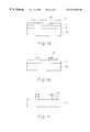
- FIGS. 1 a to 1 fare schematic cross-sectional views showing a process for forming a photoresist pattern using a polymer of the present invention.
- FIGS. 2 to 6are NMR spectra of polymers of the present invention (represented by Formulas 5 to 9) prepared in the Preparation Examples herein.
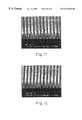
- FIGS. 7 to 14are SEM micrographs showing the appearance of photoresist patterns formed according to the present invention.
- the polymer represented by Formula 1 abovecan be prepared according to the present invention by polymerizing the following three monomers in the presence of a polymerization initiator:
- Ris a C 1 -C 10 primary, secondary or tertiary alcohol group; and m and n independently represent a number from 1 to 3.
- Preferred compounds of Formula 3are t-butyl 5-norbornene-2-carboxylate and t-butyl bicyclo[2,2,2]oct-5-ene-2-carboxylate.
- Preferred compounds of Formula 4are compounds in which R is a methyl alcohol, ethyl alcohol, propyl alcohol, butyl alcohol, or pentyl alcohol group.
- the most preferred compounds of Formula 4are 2-hydroxyethyl 5-norbornene-2-carboxylate, 3-hydroxypropyl 5-norbornene-2-carboxylate, 2-hydroxyethyl-bicyclo [2,2,2]oct-5-ene-2-carboxylate, and 3-hydroxypropyl-bicyclo[2,2,2]oct-5-ene-2-carboxylate.
- the compounds of Formula 2, Formula 3 and Formula 4are reacted in a mole ratio of 1:(0.2-0.8):(0.2-0.8) respectively.
- the polymers of the present inventioncan be manufactured at low cost, and with olefin copolymers that are easily combined using a conventional polymerization process such as bulk polymerization or solution polymerization.
- Benzoyl peroxide, 2,2-azobisisobutyronitrile (AIBN), acetyl peroxide, lauryl peroxide, or t-butyl peroxidecan be used as a polymerization initiator.
- Tetrahydrofuran (THF), cyclohexane, methyl ethyl ketone, benzene, toluene, dioxane, or dimethyl formamidecan be used as a polymerization solvent.
- the polymerizationis typically carried out at a temperature between 60° C. and 80° C. in a nitrogen or an argon atmosphere for 5 to 25 hours.
- polymerization conditionsare not limited to the above conditions.
- a photoresist compositioncan be prepared by mixing a polymer of Formula 1, a solvent, and a photoacid generator in a conventional manner.
- the photoacid generatoris preferably a sulfur salt or onium salt which is selected from the group consisting of diphenyliodo hexafluorophosphate, diphenyliodo hexafluoroarsenate, diphenyliodo hexafluoroantimonate, diphenyl p-methoxyphenyl triflate, diphenyl p-toluenyl triflate, diphenyl p-isobutylphenyl triflate, diphenyl p-t-butylphenyl triflate, triphenylsulfonium hexafluorophosphate, triphenylsulfonium hexafluoroarsenate, triphenylsulfonium hexafluoroantimonate, triphenylsulfonium triflate, and dibutylnaphthyl sulfonium triflate.
- the photoacid generatoris used in a quantity equal to about 1 to 20 wt % of the photoresist polymer used in the process.
- the sensitivity of the photoresist compositionis insufficient at quantities of photoacid generator below 1 wt % and etching resistance is insufficient at quantities over 20 wt %.
- the solvent used in the compositionmay be conventional solvents such as methyl-3-methoxypropionate, ethyl-3-ethoxypropionate, propylene glycol methyl ether acetate.
- the solventis used in a quantity equal to about 100 to 700 wt % of the polymer used in the process.
- the photoresist compositionis preferably formed into a layer with a thickness of 0.3-3 ⁇ m.
- the present inventionalso contemplates a method of forming a micro pattern using the above-described photoresist composition in a TSI process.
- a layer of the photoresist composition ( 2 )which is coated on the upper part of etching layer ( 3 ) on the surface of a wafer ( 10 ), is first hardened by methods know in the art.
- a mask ( 1 )is used to form exposed regions ( 12 ) on the hardened photoresist layer ( 2 ), and the photoresist is hardened again.
- a silylation agentis sprayed on the element to form a silylation film ( 14 ) on the exposed areas.
- Silylation film ( 14 )is subsequently developed by a dry developing process using O 2 plasma to form silicon oxide film ( 16 ).
- Etching layer ( 3 )is then etched using the silicon oxide film ( 16 ) as an etching mask to form a pattern on etching layer ( 3 ).
- FIGS. 1 a-fare cross-sectional views illustrating the method of forming a silylation photoresist pattern in a semiconductor element according to the present invention using the TSI process.
- the photoresistis baked at a temperature between 110° C. to 150° C. for 30 to 300 seconds in a first hardening step. Because the photoresist composition does not flow at high temperatures (150° C. to 190° C.) in silylation, it can form an ultra-micro pattern below 100 nm.
- the hardened photoresist layer ( 2 )is exposed through mask ( 1 ) using a light source, such as ArF, EUV, an E-beam, or an ion-beam, having an exposing energy of 1-50 mJ/cm 2 .
- a light sourcesuch as ArF, EUV, an E-beam, or an ion-beam, having an exposing energy of 1-50 mJ/cm 2 .
- the photoresistis again baked at a temperature between 110° C. and 150° C. for 30 to 300 seconds in a second hardening step.
- Reaction Foimula 1the t-butyl group of the polymer is converted to a carboxylic acid group at the exposed regions through a diffusion of acids, and isobutene gas is discharged from the photoresist as a side product.
- silylation agentIn a continuous silylation process, the discharge of isobutene allows the silylation agent to be easily permeated into the photoresist.
- suitable silylation agents for the practice of this inventionare hexamethyldisilazane, tetramethyldisilazane, dimethylaminodimethylsilane, dimethylaminoethylsilane,dimethylsilyldimethylamine, trimethylsilyldimethylamine, trimethylsilyldiethylamine, dimethylaminopentamethylsilane, and the like.
- the most preferred silylation agentis hexmethyldisilazane (HMDS).
- HMDShexmethyldisilazane
- the silylation processis preferably carried out at a temperature between 100° C. to 170° C. for 30 to 300 seconds.
- Silylation agentssuch as hexamethyldisilazane are a type of amine in which the silicon atom bound to the nitrogen atom has a powerful electron donating capacity, thereby making the silylation agent a strong base.
- hexamethyldisilazanereacts with the carboxylic acid group generated in the exposed regions of the photoresist ( 2 ) in the silylation process to form the amine salt shown in Part A of Reaction Formula 2.
- This amine salteasily reacts with a hydroxy group of a polymer to form the Si—O bond shown in the Part B of Reaction Formula 2.
- the reaction shown in Reaction Formula 2does not occur therein.
- the hexamethyldisilazaneit is not easy for the hexamethyldisilazane to permeate into the photoresist and act as a silylation agent in unexposed regions because the photoresist hardens in those regions.
- the photoresistis developed through a dry developing process using the O 2 plasma, the silicon bound to the polymer in the photoresist becomes a silicon oxide film which adheres to the wafer to form a pattern.
- the resultant productwas precipitated in an ethyl ether solvent, then the gathered precipitate was dried, and 150 gms of the desired poly(maleic anhydride/t-butyl bicyclo[2,2,2]oct-5-ene-2-carboxylate/3-hydroxypropyl bicyclo[2,2,2]oct-5-ene-2-carboxylate) polymer was obtained ata yield of about 49%.
- an etching layer ( 3 )was formed on a surface of a wafer ( 10 ), the photoresist composition prepared above was coated on the etching layer ( 3 ), and the wafer was hardened to form a photoresist layer ( 2 ) (the first hardening step).
- the photoresist compositionwas hardened by baking at 150° C. for 120 seconds after coating.
- the hardened photoresist layer ( 2 )was exposed to an exposing mask using an ArF light source. In this case, an exposing energy of 8 mJ/cm 2 was used. After exposure, the wafer was baked at 130° C. for 90 seconds.
- hexarnethyldisilazanewas sprayed at 170° C. for 150 seconds on the photoresist layer ( 2 ) to form a silylation layer ( 16 ). Then, a dry etching process using O 2 plasma was performed. A pattern of the exposed regions remained, but the photoresist layer ( 2 ) of the unexposed regions was removed. As a result, a photoresist pattern was obtained, as illustrated in FIG. 7 . As shown therein, a micro pattern having a high resolution (0.13 ⁇ m) was obtained using a low level of exposing energy and an ultra short wave light source (ArF: 193 nm).
- the photoresist pattern shown in FIG. 8(resolution 0.14 ⁇ m) was obtained using 10 gms of the poly(maleic anhydride/t-butyl 5-norbornene-2-carboxylate/3-hydroxypropyl 5-norbornene-2-carboxylate) prepared according to Preparation Example 2.
- the photoresist pattern shown in FIG. 9(resolution 0.14 ⁇ m) was obtained using 10 gms of the poly(maleic anhydride/t-butyl bicyclo[2,2,2]oct-5-ene-2-carboxylate/2-hydroxy ethyl 5-norbornene-2-carboxylate) prepared according to Preparation Example 3.
- the photoresist pattern shown in FIG. 10(resolution 0.14 ⁇ m) was obtained using 10 gms of the poly(maleic anhydridelt-butyl bicyclo[2,2,2]oct-5-ene-2-arboxylate/3-hydroxypropyl 5-norbornene-2-carboxylate) prepared according to Preparation Example 4.
- the photoresist pattern shown in FIG. 11(resolution 0.14 ⁇ m) was obtained using 10 gms of the poly (maleic anhydride/t-butyl 5-norbornene-2-carboxylate/2-hydroxyethyl bicyclo[2,2,2]oct-5-ene-2-carboxylate) prepared according to Preparation Example 5 (10 g).
- the photoresist pattern shown in FIG. 12(resolution 0.14 ⁇ m) was obtained using 10 gms of the poly (maleic anhydride/t-butyl 5-norbomene-2-carboxylate/3-hydroxypropyl bicyclo[2,2,2]oct-5-ene-2-carboxylate) prepared according to Preparation Example 6.
- the photoresist pattern shown in FIG. 13(resolution 0.14 ⁇ m) was obtained using 10 gms of the poly(maleic anhydride/t-butyl bicyclo[2,2,2]oct-5-ene-2-arboxylate/2-hydroxyethyl bicyclo[2,2,2]oct-5-ene-2-carboxylate) prepared according to Preparation Example 7.
- the photoresist pattern shown in FIG. 14(resolution 0.14 ⁇ m) was obtained using 10 gms of the poly (maleic anhydride/t-butyl bicyclo[2,2,2]oct-5-ene-2-carboxylate/3-hydroxy propyl bicyclo[2,2,2]oct-5-ene-2-carboxylate) prepared according to Preparation Example 8.
- an ArF photoresistis provided in accordance with the present invention which has heat resistance sufficient to endure the post-baking and silylation processes which are carried out at a high temperature in the TSI process.
- the pattern using a chemically amplified photoresist of the present inventionis resolved through the usage of a small energy level of 10 mJ/cm 2 thereby preventing the damage that occurs to the lens of an exposer when an ArF light source is used.
- O 2 plasmais used in the silylation process with a polymer of the present invention, a silicon oxide film is formed thereby increasing etching resistance and heat resistance of the photoresist.
- a micro patterncan be formed through the dry developing process and high integration of a semiconductor element is possible through the use of a photoresist employing a polymer of the present invention.
Landscapes
- Chemical & Material Sciences (AREA)
- Physics & Mathematics (AREA)
- Medicinal Chemistry (AREA)
- Health & Medical Sciences (AREA)
- Chemical Kinetics & Catalysis (AREA)
- Polymers & Plastics (AREA)
- Organic Chemistry (AREA)
- General Physics & Mathematics (AREA)
- Spectroscopy & Molecular Physics (AREA)
- General Chemical & Material Sciences (AREA)
- Materials For Photolithography (AREA)
- Addition Polymer Or Copolymer, Post-Treatments, Or Chemical Modifications (AREA)
- Exposure And Positioning Against Photoresist Photosensitive Materials (AREA)
- Photosensitive Polymer And Photoresist Processing (AREA)
Abstract
The present invention relates to a polymer represented by following Formula 1 and a method of forming a micro pattern using the same:

wherein, R is C1-C10primary or secondary alcohol group; m and n independently represent a number from 1 to 3; and the ratio a:b:c is (10-80)mol %:(10-80)mol %:(10-80)mol %, respectively.
The photoresist polymer according to the present invention is suitable for forming an ultra-micro pattern such as used in 4G or 16G DRAM semiconductor devices using a light source such as ArF, an E-beam, EUV, or an ion-beam.
Description
The present invention relates to a polymer useful as a photoresist in a lithographic process for fabricating a semiconductor device, and a method of forming a micro pattern using the same. More specifically, the present invention relates to a polymer which can be used in a photoresist composition for forming an ultra-micro pattern in the manufacture of 4G and 16G DRAM semiconductor chips using short wavelength light sources, such as KrF (248 mn), ArF (193 nm), an E-beam, or an ion-beam. The polymer of the present invention is particularity useful in a photoresist composition for the top surface image (TSI) process using silylation.
In the manufacturing process of a semiconductor element, a photoresist is generally used to form a pattern with a fixed form on a semiconductor element. To obtain the desired photoresist pattern, a photoresist solution is coated on a surface of a semiconductor wafer, the coated photoresist is exposed to patterned light, and then the wafer undergoes a developing process. As a result, a photoresist pattern is formed on the wafer.
If the photoresist pattern is manufactured using a conventional silylation process, the photoresist is usually composed of diazonaphtoquinones compounds and a novolac resin, or a photo acid generator and polyvinyl phenol resin. When the photoresist resin is exposed to the patterned light source (e.g. ArF, KrF, or I line) and then baked, an alcohol group (R—O—H) is formed in the resin at the exposed regions. After baking, the photoresist resin is silylated with a silylation agent such as hexamethyl disilazane or tetramethyl disilazane. In the silylation process, an N—Si bond is first formed, but since the N—Si bond is weak, it then reacts with the R—O—H group in the photoresist polymer to form a R—O—Si bond. The photoresist resin with bonded silicon atoms then undergoes a dry developing using O2plasma to form a silicon oxide film. The lower portions of the silicon oxide film remain even after the development of the photoresist and as a result, the desired pattern is formed.
The above-described silylation process for forming a photoresist pattern has several deficiencies when it is used with shorter wavelength radiation. In particular, when a KrF eximer laser is used as the light source to expose known photoresist polymers, it is impossible to form an ultra-micro pattern less than 0.10 μm L/S using the silylation process. When an ArF light source is used, the lens of the exposer can be damaged due to the high energy level of the ArF light. Therefore, the photoresist must be exposed to a lower amount of energy, for example, less than 10 mJ/cm2. If the photoresist is not exposed sufficiently to this lower energy, the desired pattern is not formed.
It has been found that the unique photoresist polymers of the present invention solve the above-described problems of the prior art. The heat-resistant character of the polymers of this invention allow the high temperatures required by the post-exposure baking and silylation steps of the TSI process to be obtained. The polymers of the present invention are particularity suited for use in chemically amplied photoresists wherein a photoresist pattern can be resolved even using a small amount of energy (e.g., 10 mJ/cm2), thereby preventing the damage to the lens of the exposer and the photoresist pattern collapse or insufficient resolution which occurs in the prior art during the formation of the micro pattern using an ArF (193 nm) light source. In addition, the polymers of the present invention are advantageously used in the silylation process wherein a chemically amplified photoresist and O2plasma are used to form a silicon oxide film which increases the etching and heat resistance of the photoresist such that an acceptable micro pattern can be formed using the dry developing process.
In one embodiment, the present invention relates to a polymer which is suitable for use as a single layer photoresist, and preferably as a photoresist in the TSI process. Preferred photoresist polymers of the present invention are represented by the following Formula 1:

wherein, R is a C1-C10primary or secondary alcohol group; m and n independently represent a number from 1 to 3; and the ratio of a:b:c is (10-100):(10-90):(10-90).
Another embodiment of the present invention relates to a preparation method for the polymer represented by the above Formula 1.
In still another embodiment, the present invention relates to a photoresist composition containing the polymer represented by theabove Formula 1, a solvent, and a photoacid generator.
In a further embodiment, the present invention relates to a method of forming a micro pattern using the above-described photoresist composition.
FIGS. 1ato1fare schematic cross-sectional views showing a process for forming a photoresist pattern using a polymer of the present invention.
FIGS. 2 to6 are NMR spectra of polymers of the present invention (represented by Formulas 5 to 9) prepared in the Preparation Examples herein.
FIGS. 7 to14 are SEM micrographs showing the appearance of photoresist patterns formed according to the present invention.
The polymer represented by Formula 1 above can be prepared according to the present invention by polymerizing the following three monomers in the presence of a polymerization initiator:


wherein, R is a C1-C10primary, secondary or tertiary alcohol group; and m and n independently represent a number from 1 to 3.
Preferred compounds of Formula 3 are t-butyl 5-norbornene-2-carboxylate and t-butyl bicyclo[2,2,2]oct-5-ene-2-carboxylate.
Preferred compounds of Formula 4 are compounds in which R is a methyl alcohol, ethyl alcohol, propyl alcohol, butyl alcohol, or pentyl alcohol group. The most preferred compounds ofFormula 4 are 2-hydroxyethyl 5-norbornene-2-carboxylate, 3-hydroxypropyl 5-norbornene-2-carboxylate, 2-hydroxyethyl-bicyclo [2,2,2]oct-5-ene-2-carboxylate, and 3-hydroxypropyl-bicyclo[2,2,2]oct-5-ene-2-carboxylate.
According to a preferred embodiment of the present invention, the compounds of Formula 2, Formula 3 and Formula 4 are reacted in a mole ratio of 1:(0.2-0.8):(0.2-0.8) respectively.
The polymers of the present invention can be manufactured at low cost, and with olefin copolymers that are easily combined using a conventional polymerization process such as bulk polymerization or solution polymerization. Benzoyl peroxide, 2,2-azobisisobutyronitrile (AIBN), acetyl peroxide, lauryl peroxide, or t-butyl peroxide can be used as a polymerization initiator. Tetrahydrofuran (THF), cyclohexane, methyl ethyl ketone, benzene, toluene, dioxane, or dimethyl formamide can be used as a polymerization solvent. The polymerization is typically carried out at a temperature between 60° C. and 80° C. in a nitrogen or an argon atmosphere for 5 to 25 hours. However, polymerization conditions are not limited to the above conditions.
The polymers of Formula 1, prepared according to the above polymerization process, are useful as photoresists for forming a micro pattern in the fabrication of a semiconductor element. According to the present invention, a photoresist composition can be prepared by mixing a polymer of Formula 1, a solvent, and a photoacid generator in a conventional manner. The photoacid generator is preferably a sulfur salt or onium salt which is selected from the group consisting of diphenyliodo hexafluorophosphate, diphenyliodo hexafluoroarsenate, diphenyliodo hexafluoroantimonate, diphenyl p-methoxyphenyl triflate, diphenyl p-toluenyl triflate, diphenyl p-isobutylphenyl triflate, diphenyl p-t-butylphenyl triflate, triphenylsulfonium hexafluorophosphate, triphenylsulfonium hexafluoroarsenate, triphenylsulfonium hexafluoroantimonate, triphenylsulfonium triflate, and dibutylnaphthyl sulfonium triflate. The photoacid generator is used in a quantity equal to about 1 to 20 wt % of the photoresist polymer used in the process. The sensitivity of the photoresist composition is insufficient at quantities of photoacid generator below 1 wt % and etching resistance is insufficient at quantities over 20 wt %. The solvent used in the composition may be conventional solvents such as methyl-3-methoxypropionate, ethyl-3-ethoxypropionate, propylene glycol methyl ether acetate. The solvent is used in a quantity equal to about 100 to 700 wt % of the polymer used in the process. The photoresist composition is preferably formed into a layer with a thickness of 0.3-3 μm.
The present invention also contemplates a method of forming a micro pattern using the above-described photoresist composition in a TSI process. Generally in this process, as illustrated in FIGS. 1ato1f, a layer of the photoresist composition (2), which is coated on the upper part of etching layer (3) on the surface of a wafer (10), is first hardened by methods know in the art. A mask (1) is used to form exposed regions (12) on the hardened photoresist layer (2), and the photoresist is hardened again. Then, a silylation agent is sprayed on the element to form a silylation film (14) on the exposed areas. Silylation film (14) is subsequently developed by a dry developing process using O2plasma to form silicon oxide film (16). Etching layer (3) is then etched using the silicon oxide film (16) as an etching mask to form a pattern on etching layer (3).
The present invention is explained in more detail below, referring to the attached figures.
As stated, FIGS. 1a-fare cross-sectional views illustrating the method of forming a silylation photoresist pattern in a semiconductor element according to the present invention using the TSI process. After etching layer (3) and photoresist layer (2) are coated on the surface of wafer (10), the photoresist is baked at a temperature between 110° C. to 150° C. for 30 to 300 seconds in a first hardening step. Because the photoresist composition does not flow at high temperatures (150° C. to 190° C.) in silylation, it can form an ultra-micro pattern below 100 nm. The hardened photoresist layer (2) is exposed through mask (1) using a light source, such as ArF, EUV, an E-beam, or an ion-beam, having an exposing energy of 1-50 mJ/cm2. After exposure, the photoresist is again baked at a temperature between 110° C. and 150° C. for 30 to 300 seconds in a second hardening step. As a result, as illustrated inReaction Foimula 1 below, the t-butyl group of the polymer is converted to a carboxylic acid group at the exposed regions through a diffusion of acids, and isobutene gas is discharged from the photoresist as a side product.

In a continuous silylation process, the discharge of isobutene allows the silylation agent to be easily permeated into the photoresist. Examples of suitable silylation agents for the practice of this invention are hexamethyldisilazane, tetramethyldisilazane, dimethylaminodimethylsilane, dimethylaminoethylsilane,dimethylsilyldimethylamine, trimethylsilyldimethylamine, trimethylsilyldiethylamine, dimethylaminopentamethylsilane, and the like. The most preferred silylation agent is hexmethyldisilazane (HMDS). The silylation process is preferably carried out at a temperature between 100° C. to 170° C. for 30 to 300 seconds.
Where the photoresist is used in the TSI process according to the present invention, the silylation reaction is facilitated by the carboxylic acid group formed on the photoresist polymer. This reaction principle is illustrated inReaction Formula 2.

Silylation agents such as hexamethyldisilazane are a type of amine in which the silicon atom bound to the nitrogen atom has a powerful electron donating capacity, thereby making the silylation agent a strong base. For example, hexamethyldisilazane reacts with the carboxylic acid group generated in the exposed regions of the photoresist (2) in the silylation process to form the amine salt shown in Part A ofReaction Formula 2. This amine salt easily reacts with a hydroxy group of a polymer to form the Si—O bond shown in the Part B ofReaction Formula 2. However, because the carboxylic acid group is not generated in unexposed regions of the photoresist polymer, the reaction shown inReaction Formula 2 does not occur therein. Furthermore, it is not easy for the hexamethyldisilazane to permeate into the photoresist and act as a silylation agent in unexposed regions because the photoresist hardens in those regions. When the photoresist is developed through a dry developing process using the O2plasma, the silicon bound to the polymer in the photoresist becomes a silicon oxide film which adheres to the wafer to form a pattern.
A better understanding of the present invention may be obtained by reference to the following examples which are set forth to illustrate, but not limit, the present invention.

Maleic anhydride (1 mol.), t-butyl 5-norbornene-2-carboxylate (0.5 mol.) and 2-hydroxyethyl 5-norbornene-2-carboxylate (0.5 mol) were dissolved in 220 gms of tetrahydrofuran (THF), 5.7 gms of 2,2′-azobisisobutyronitrile (AIBN) was added thereto, and the resulting solution was reacted at a temperature of 67° C. in a nitrogen atmosphere for 10 hours. After a high molecular weight was achieved by the reaction, the resultant product was precipitated in an ethyl ether solvent. The gathered precipitate was dried, and about 170 gms of the desired poly(maleic anhydride-butyl 5-norbornene-2-carboxylate/2-hydroxyethyl 5-norbornene-2-carboxylate) polymer was obtained at a yield of about 60%. NMR spectra of the polymer is illustrated in FIG.2.

Maleic anhydride (1 mol.), t-butyl 5-norbornene-2-carboxylate (0.5 mol.), and 3-hydroxy propyl 5-norbornene-2-carboxylate (0.5 mol.) were dissolved in 200 gms. of tetrahydrofuran (THF), 6 gms. of 2,2′-azobisisobutyronitrile (AIBN) were added thereto, then the resultant solution was reacted at a temperature of 67° C. in a nitrogen atmosphere for 10 hours. After a high molecular weight was achieved by the reaction, the resultant product was precipitated in an ethyl ether solvent. The gathered precipitate was dried, and about 167 grams of the desired poly (maleic anhydride/t-butyl 5-norbornene-2-carboxylate/3-hydroxypropyl 5-norbornene-2-carboxylate) polymer was obtained at a yield of about 57%. NMR spectra of the polymer is illustrated in FIG.3.


Maleic anhydride (1 mol.), t-butyl bicyclo[2,2,2]oct-5-ene-2-carboxylate (0.5 mol.), and 3-hydroxy propyl 5-norbornene-2-carboxylate (0.5 mol.) were dissolved in 200 gms of tetrahydrofuran (THF), 6 gms of 2,2′-azobisisobutyronitrile (AIBN) was added thereto, and then the resultant solution was reacted at a temperature of 67° C. in a nitrogen atmosphere for 10 hours. After a high molecule weight was achieved by the reaction, the resultant product was precipitated in an ethyl ether solvent. The gathered precipitate was dried, and 150 gms of the desirable poly(maleic anhydride/t-butyl bicyclo[2,2,2]oct-5-ene-2-carboxylate/3-hydroxypropyl 5-norbornene-2-carboxylate) polymer was obtained at a yield of about 50%. NMR spectra of the polymer is illustrated in FIG.5.

Maleic anhydride (1 mol.), t-butyl 5-norbornene-2-carboxylate (0.5 mol.) and 2-hydroxy ethyl bicyclo[2,2,2]oct-5-ene-2-carboxylate (0.5 mol.) were dissolved in 200 gms of tetrahydrofuran (THF), 6 gms of 2,2′-azobisisobutyronitrile (AIBN) was added thereto, then the resultant solution was reacted at a temperature of 67° C. in a nitrogen atmosphere for 10 hours. After a high molecule weight was achieved by the reaction, the resultant product was precipitated in an ethyl ether solvent. The gathered precipitate was dried, and 150 gms of the desired poly(maleic anhydride/t-butyl 5-norbornene-2-carboxylate/2-hydroxyethyl bicyclo[2,2,2]oct-5-ene-2-carboxylate) polymer was obtained at a yield of about 51%. NMR spectra of the polymer is illustrated in FIG.6.

Maleic anhydride (1 mol.), t-butyl 5-norbornene-2-carboxylate (0.5 mol.) and 3-hydroxypropylbicyclo[2,2,2]oct-5-ene-2-carboxylate (0.5 mol.) were dissolved in 200 gms of tetrahydrofuran (THF), 6 gms of 2,2′-azobisisobutyronitrile (AIBN) was added thereto, then the resultant solution was reacted at a temperature between 60° C. and 70° C. in a nitrogen atnosphere for 10 hours. After a high molecule weight was achieved by the reaction, the resultant product was precipitated in an ethyl ether solvent. The gathered precipitate was dried, and 168 gms of the desired poly(maleic anhydride-butyl 5-norbornene-2-carboxylate/3-hydoxyproply bicyclo[2,2,2]oct-5-ene-2-carboxylate) polymer was obtained at a yield of about 56%.

Maleic anhydride (1 mol.), t-butyl bicyclo[2,2,2]oct-5-ene-2-carboxylate (0.5 mol.), and 2-hydroxyethyl bicyclo[2,2,2]oct-5-ened-2-carboxylate (0.5 mol.) were dissolved in 200 gms of tetrrhydrofuran (THF), 6 gms of 2,2′-azobisisobutyronitrile (AIBN) was added thereto, then the resultant solution was reacted at a temperature of 67° C. in a nitrogen atmosphere for 10 hours. After a high molecular weight was achieved by the reaction, the resultant product was precipitated in an ethyl ether solvent. The gathered precipitate was dried, and 156 gms of the desired poly(maleic anhydride/t-butyl bicyclo[2,2,2]oct-5-ene-2-carboxylate/2-hydroxyethyl bicyclo[2,2,2]oct-5-ene-2-carboxylate) polymer was obtained at a yield of about 52%.

Maleic anhydride (1 mol.), t-butyl bicyclo[2,2,2]oct-5-ene-2-carboxylate (0.5 mol.), and 3-hydroxypropyl bicyclo[2,2,2]oct-5-ene-2-carboxylate (0.5 mol.) were dissolved in 200 gins of tetrahydrofuran (THF), 6 gms of 2,2′-azobisisobutyronitrile (AIBN) was added thereto, then the resultant solution was reacted at a temperature of 67° C. in a nitrogen atmosphere for 10 hours. After a high molecular weight was achievd by reaction, the resultant product was precipitated in an ethyl ether solvent, then the gathered precipitate was dried, and 150 gms of the desired poly(maleic anhydride/t-butyl bicyclo[2,2,2]oct-5-ene-2-carboxylate/3-hydroxypropyl bicyclo[2,2,2]oct-5-ene-2-carboxylate) polymer was obtained ata yield of about 49%.
10 gms of poly (maleic anhydride/t-butyl 5-norbornene-2-carboxylate/2-hydroxy ethyl 5-norbornene-2-carboxylate), prepared according to Preparation Example 1, were dissolved in 40 gms of ethyl 3-ethoxypropionate as a solvent,and 0.4 gms of triphenylsulfonium triflate were added thereto. Then the resultant solution was filtered through filter of 0.10 μm to prepare a photoresist composition.
Referring to FIGS. 1ato1f, an etching layer (3) was formed on a surface of a wafer (10), the photoresist composition prepared above was coated on the etching layer (3), and the wafer was hardened to form a photoresist layer (2) (the first hardening step). In this case, the photoresist composition was hardened by baking at 150° C. for 120 seconds after coating. Subsequently, the hardened photoresist layer (2) was exposed to an exposing mask using an ArF light source. In this case, an exposing energy of 8 mJ/cm2was used. After exposure, the wafer was baked at 130° C. for 90 seconds. Subsequently, hexarnethyldisilazane was sprayed at 170° C. for 150 seconds on the photoresist layer (2) to form a silylation layer (16). Then, a dry etching process using O2plasma was performed. A pattern of the exposed regions remained, but the photoresist layer (2) of the unexposed regions was removed. As a result, a photoresist pattern was obtained, as illustrated in FIG.7. As shown therein, a micro pattern having a high resolution (0.13 μm) was obtained using a low level of exposing energy and an ultra short wave light source (ArF: 193 nm).
According to the method of Example 1 above, the photoresist pattern shown in FIG. 8 (resolution 0.14 μm) was obtained using 10 gms of the poly(maleic anhydride/t-butyl 5-norbornene-2-carboxylate/3-hydroxypropyl 5-norbornene-2-carboxylate) prepared according to Preparation Example 2.
According to the method of Example 1 above, the photoresist pattern shown in FIG. 9 (resolution 0.14 μm) was obtained using 10 gms of the poly(maleic anhydride/t-butyl bicyclo[2,2,2]oct-5-ene-2-carboxylate/2-hydroxy ethyl 5-norbornene-2-carboxylate) prepared according to Preparation Example 3.
According to the method of Example 1 above, the photoresist pattern shown in FIG. 10 (resolution 0.14 μm) was obtained using 10 gms of the poly(maleic anhydridelt-butyl bicyclo[2,2,2]oct-5-ene-2-arboxylate/3-hydroxypropyl 5-norbornene-2-carboxylate) prepared according to Preparation Example 4.
According to the method of Example 1 above, the photoresist pattern shown in FIG. 11 (resolution 0.14 μm) was obtained using 10 gms of the poly (maleic anhydride/t-butyl 5-norbornene-2-carboxylate/2-hydroxyethyl bicyclo[2,2,2]oct-5-ene-2-carboxylate) prepared according to Preparation Example 5 (10 g).
According to the method of Example 1, the photoresist pattern shown in FIG. 12 (resolution 0.14 μm) was obtained using 10 gms of the poly (maleic anhydride/t-butyl 5-norbomene-2-carboxylate/3-hydroxypropyl bicyclo[2,2,2]oct-5-ene-2-carboxylate) prepared according to Preparation Example 6.
According to the method of Example 1, the photoresist pattern shown in FIG. 13 (resolution 0.14 μm) was obtained using 10 gms of the poly(maleic anhydride/t-butyl bicyclo[2,2,2]oct-5-ene-2-arboxylate/2-hydroxyethyl bicyclo[2,2,2]oct-5-ene-2-carboxylate) prepared according to Preparation Example 7.
According to the method of Example 1, the photoresist pattern shown in FIG. 14 (resolution 0.14 μm) was obtained using 10 gms of the poly (maleic anhydride/t-butyl bicyclo[2,2,2]oct-5-ene-2-carboxylate/3-hydroxy propyl bicyclo[2,2,2]oct-5-ene-2-carboxylate) prepared according to Preparation Example 8.
As described above, an ArF photoresist is provided in accordance with the present invention which has heat resistance sufficient to endure the post-baking and silylation processes which are carried out at a high temperature in the TSI process. Also, the pattern using a chemically amplified photoresist of the present invention is resolved through the usage of a small energy level of 10 mJ/cm2thereby preventing the damage that occurs to the lens of an exposer when an ArF light source is used. When O2plasma is used in the silylation process with a polymer of the present invention, a silicon oxide film is formed thereby increasing etching resistance and heat resistance of the photoresist. Thus, a micro pattern can be formed through the dry developing process and high integration of a semiconductor element is possible through the use of a photoresist employing a polymer of the present invention.
Other features, such as other advantages and embodiments, of the invention disclosed herein will be readily apparent to those of ordinary skill in the art after reading the foregoing disclosures. In this regard, while specific embodiments of the invention have been described in considerable detail, variations and modifications of these embodiments can be effected without departing from the spirit and scope of the invention as described and claimed.
Claims (7)
1. A method of forming a photoresist pattern, comprising the steps of:
a) preparing a photoresist composition comprising:

wherein, R is a C1-C10primary or secondary alcohol group; m and n independently represent a number from 1 to 3; and a, b and c are the respective polymerization ratios of the co-monomers; wherein each of a:b:c: is greater than 0 AND represent polymerization ratios of the co-monomers.
(ii) a photoacid generator, and,
(iii) an organic solvent.
b) coating the photoresist composition on a substrate having an etching layer coated on the surface thereof;
c) exposing the photoresist layer to a light source using an exposer to form a pattern of exposed regions in the photoresist layer wherein the photoresist polymer contains free carboxylic acid groups;
d) spraying a silylation agent on the pattern in photoresist layer;
e) dry etching the resultant pattern to form a pattern in the substrate.

3. A method of forming a photoresist pattern in accordance with claim1, which further comprises abaking step before and/or after the (c) step, wherein the baking is carried out at 110° C. to 150° C. for 30 to 300 seconds.
4. A method of forming a photoresist pattern in accordance with claim1, wherein the (c) step is carried out by using an ArF, EUV, E-beam, ion-bearn, or X-ray light source.
5. A method of forming a photoresist pattern in accordance with claim1, wherein the (c) step is carried out using irradiating energy of 1-50 mJ/cm2.
6. A method of forming a photoresist pattern in accordance with claim1, wherein the silylation agent is selected from the group consisting of hexamethyldisilazane, tetramethyldisiazane, dimethylaminomethylsilane, dimethylaaminomethylsilane, dimethylsilyldimethylamine, trimethylsilyldimethylamine, trimethylsilyldiethylamine and dimethylaminopentamethylsilane.
7. A method of forming a photoresist pattern in accordance with claim1, wherein the (d) step is carried out at 100° C. to 170° C. for 30 to 300 seconds.
Applications Claiming Priority (2)
| Application Number | Priority Date | Filing Date | Title |
|---|---|---|---|
| KR98-16221 | 1998-04-30 | ||
| KR1019980016221AKR100376983B1 (en) | 1998-04-30 | 1998-04-30 | Photoresist polymer and method for forming micropattern by using the same |
Publications (1)
| Publication Number | Publication Date |
|---|---|
| US6316162B1true US6316162B1 (en) | 2001-11-13 |
Family
ID=19537080
Family Applications (1)
| Application Number | Title | Priority Date | Filing Date |
|---|---|---|---|
| US09/301,945Expired - Fee RelatedUS6316162B1 (en) | 1998-04-30 | 1999-04-29 | Polymer and a forming method of a micro pattern using the same |
Country Status (6)
| Country | Link |
|---|---|
| US (1) | US6316162B1 (en) |
| JP (1) | JP3895886B2 (en) |
| KR (1) | KR100376983B1 (en) |
| CN (1) | CN1221856C (en) |
| DE (1) | DE19919794A1 (en) |
| GB (1) | GB2336845B (en) |
Cited By (362)
| Publication number | Priority date | Publication date | Assignee | Title |
|---|---|---|---|---|
| US6472120B1 (en)* | 1999-07-29 | 2002-10-29 | Samsung Electronics Co., Ltd. | Photosensitive polymer and chemically amplified photoresist composition containing the same |
| US20030091927A1 (en)* | 2001-08-24 | 2003-05-15 | Hynix Semiconductor Inc. | Photoresist monomers, polymers and photoresist compositions for preventing acid diffusion |
| US6586619B2 (en) | 1998-08-26 | 2003-07-01 | Hyundai Electronics Industries Co., Ltd. | Photoresist monomer having hydroxy group and carboxy group, copolymer thereof and photoresist composition using the same |
| US20030191259A1 (en)* | 1998-08-27 | 2003-10-09 | Hyundai Electronics Industries Co., Ltd. | Novel polymers for photoresist and photoresist compositions using the same |
| US6642336B1 (en)* | 1999-08-24 | 2003-11-04 | Samsung Electronics Co., Ltd. | Photosensitive polymer |
| US20040131968A1 (en)* | 1996-12-21 | 2004-07-08 | Hyundai Electronics Industries Co., Ltd. | Novel ArF photoresist copolymers |
| US20050019693A1 (en)* | 1999-07-29 | 2005-01-27 | Dong-Won Jung | Photosensitive polymer and chemically amplified photoresist composition containing the same |
| US20090191709A1 (en)* | 2005-06-02 | 2009-07-30 | Hynix Semiconductor Inc. | Method for Manufacturing a Semiconductor Device |
| US8980537B2 (en) | 2011-09-05 | 2015-03-17 | Stmicroelectronics (Crolles 2) Sas | Photolithography method using a chemically-amplified resist |
| WO2018167170A1 (en)* | 2017-03-15 | 2018-09-20 | Flexenable Limited | Cross-linked polymers |
| US10083836B2 (en) | 2015-07-24 | 2018-09-25 | Asm Ip Holding B.V. | Formation of boron-doped titanium metal films with high work function |
| US10134757B2 (en) | 2016-11-07 | 2018-11-20 | Asm Ip Holding B.V. | Method of processing a substrate and a device manufactured by using the method |
| US10229833B2 (en) | 2016-11-01 | 2019-03-12 | Asm Ip Holding B.V. | Methods for forming a transition metal nitride film on a substrate by atomic layer deposition and related semiconductor device structures |
| US10249524B2 (en) | 2017-08-09 | 2019-04-02 | Asm Ip Holding B.V. | Cassette holder assembly for a substrate cassette and holding member for use in such assembly |
| US10249577B2 (en) | 2016-05-17 | 2019-04-02 | Asm Ip Holding B.V. | Method of forming metal interconnection and method of fabricating semiconductor apparatus using the method |
| US10262859B2 (en) | 2016-03-24 | 2019-04-16 | Asm Ip Holding B.V. | Process for forming a film on a substrate using multi-port injection assemblies |
| US10269558B2 (en) | 2016-12-22 | 2019-04-23 | Asm Ip Holding B.V. | Method of forming a structure on a substrate |
| US10276355B2 (en) | 2015-03-12 | 2019-04-30 | Asm Ip Holding B.V. | Multi-zone reactor, system including the reactor, and method of using the same |
| US10283353B2 (en) | 2017-03-29 | 2019-05-07 | Asm Ip Holding B.V. | Method of reforming insulating film deposited on substrate with recess pattern |
| US10290508B1 (en) | 2017-12-05 | 2019-05-14 | Asm Ip Holding B.V. | Method for forming vertical spacers for spacer-defined patterning |
| US10312055B2 (en) | 2017-07-26 | 2019-06-04 | Asm Ip Holding B.V. | Method of depositing film by PEALD using negative bias |
| US10312129B2 (en) | 2015-09-29 | 2019-06-04 | Asm Ip Holding B.V. | Variable adjustment for precise matching of multiple chamber cavity housings |
| US10319588B2 (en) | 2017-10-10 | 2019-06-11 | Asm Ip Holding B.V. | Method for depositing a metal chalcogenide on a substrate by cyclical deposition |
| US10322384B2 (en) | 2015-11-09 | 2019-06-18 | Asm Ip Holding B.V. | Counter flow mixer for process chamber |
| US10340135B2 (en) | 2016-11-28 | 2019-07-02 | Asm Ip Holding B.V. | Method of topologically restricted plasma-enhanced cyclic deposition of silicon or metal nitride |
| US10340125B2 (en) | 2013-03-08 | 2019-07-02 | Asm Ip Holding B.V. | Pulsed remote plasma method and system |
| US10343920B2 (en) | 2016-03-18 | 2019-07-09 | Asm Ip Holding B.V. | Aligned carbon nanotubes |
| US10361201B2 (en) | 2013-09-27 | 2019-07-23 | Asm Ip Holding B.V. | Semiconductor structure and device formed using selective epitaxial process |
| US10366864B2 (en) | 2013-03-08 | 2019-07-30 | Asm Ip Holding B.V. | Method and system for in-situ formation of intermediate reactive species |
| US10367080B2 (en) | 2016-05-02 | 2019-07-30 | Asm Ip Holding B.V. | Method of forming a germanium oxynitride film |
| US10364496B2 (en) | 2011-06-27 | 2019-07-30 | Asm Ip Holding B.V. | Dual section module having shared and unshared mass flow controllers |
| US10381226B2 (en) | 2016-07-27 | 2019-08-13 | Asm Ip Holding B.V. | Method of processing substrate |
| US10378106B2 (en) | 2008-11-14 | 2019-08-13 | Asm Ip Holding B.V. | Method of forming insulation film by modified PEALD |
| US10381219B1 (en) | 2018-10-25 | 2019-08-13 | Asm Ip Holding B.V. | Methods for forming a silicon nitride film |
| US10388509B2 (en) | 2016-06-28 | 2019-08-20 | Asm Ip Holding B.V. | Formation of epitaxial layers via dislocation filtering |
| US10388513B1 (en) | 2018-07-03 | 2019-08-20 | Asm Ip Holding B.V. | Method for depositing silicon-free carbon-containing film as gap-fill layer by pulse plasma-assisted deposition |
| US10395919B2 (en) | 2016-07-28 | 2019-08-27 | Asm Ip Holding B.V. | Method and apparatus for filling a gap |
| US10403504B2 (en) | 2017-10-05 | 2019-09-03 | Asm Ip Holding B.V. | Method for selectively depositing a metallic film on a substrate |
| US10410943B2 (en) | 2016-10-13 | 2019-09-10 | Asm Ip Holding B.V. | Method for passivating a surface of a semiconductor and related systems |
| US10438965B2 (en) | 2014-12-22 | 2019-10-08 | Asm Ip Holding B.V. | Semiconductor device and manufacturing method thereof |
| US10435790B2 (en) | 2016-11-01 | 2019-10-08 | Asm Ip Holding B.V. | Method of subatmospheric plasma-enhanced ALD using capacitively coupled electrodes with narrow gap |
| US10446393B2 (en) | 2017-05-08 | 2019-10-15 | Asm Ip Holding B.V. | Methods for forming silicon-containing epitaxial layers and related semiconductor device structures |
| US10458018B2 (en) | 2015-06-26 | 2019-10-29 | Asm Ip Holding B.V. | Structures including metal carbide material, devices including the structures, and methods of forming same |
| US10468261B2 (en) | 2017-02-15 | 2019-11-05 | Asm Ip Holding B.V. | Methods for forming a metallic film on a substrate by cyclical deposition and related semiconductor device structures |
| US10468251B2 (en) | 2016-02-19 | 2019-11-05 | Asm Ip Holding B.V. | Method for forming spacers using silicon nitride film for spacer-defined multiple patterning |
| US10483099B1 (en) | 2018-07-26 | 2019-11-19 | Asm Ip Holding B.V. | Method for forming thermally stable organosilicon polymer film |
| US10480072B2 (en) | 2009-04-06 | 2019-11-19 | Asm Ip Holding B.V. | Semiconductor processing reactor and components thereof |
| US10504742B2 (en) | 2017-05-31 | 2019-12-10 | Asm Ip Holding B.V. | Method of atomic layer etching using hydrogen plasma |
| US10501866B2 (en) | 2016-03-09 | 2019-12-10 | Asm Ip Holding B.V. | Gas distribution apparatus for improved film uniformity in an epitaxial system |
| US10510536B2 (en) | 2018-03-29 | 2019-12-17 | Asm Ip Holding B.V. | Method of depositing a co-doped polysilicon film on a surface of a substrate within a reaction chamber |
| US10529554B2 (en) | 2016-02-19 | 2020-01-07 | Asm Ip Holding B.V. | Method for forming silicon nitride film selectively on sidewalls or flat surfaces of trenches |
| US10529563B2 (en) | 2017-03-29 | 2020-01-07 | Asm Ip Holdings B.V. | Method for forming doped metal oxide films on a substrate by cyclical deposition and related semiconductor device structures |
| US10529542B2 (en) | 2015-03-11 | 2020-01-07 | Asm Ip Holdings B.V. | Cross-flow reactor and method |
| US10535516B2 (en) | 2018-02-01 | 2020-01-14 | Asm Ip Holdings B.V. | Method for depositing a semiconductor structure on a surface of a substrate and related semiconductor structures |
| US10541333B2 (en) | 2017-07-19 | 2020-01-21 | Asm Ip Holding B.V. | Method for depositing a group IV semiconductor and related semiconductor device structures |
| US10541173B2 (en) | 2016-07-08 | 2020-01-21 | Asm Ip Holding B.V. | Selective deposition method to form air gaps |
| US10559458B1 (en) | 2018-11-26 | 2020-02-11 | Asm Ip Holding B.V. | Method of forming oxynitride film |
| US10566223B2 (en) | 2012-08-28 | 2020-02-18 | Asm Ip Holdings B.V. | Systems and methods for dynamic semiconductor process scheduling |
| US10561975B2 (en) | 2014-10-07 | 2020-02-18 | Asm Ip Holdings B.V. | Variable conductance gas distribution apparatus and method |
| US10590535B2 (en) | 2017-07-26 | 2020-03-17 | Asm Ip Holdings B.V. | Chemical treatment, deposition and/or infiltration apparatus and method for using the same |
| US10600673B2 (en) | 2015-07-07 | 2020-03-24 | Asm Ip Holding B.V. | Magnetic susceptor to baseplate seal |
| US10605530B2 (en) | 2017-07-26 | 2020-03-31 | Asm Ip Holding B.V. | Assembly of a liner and a flange for a vertical furnace as well as the liner and the vertical furnace |
| US10607895B2 (en) | 2017-09-18 | 2020-03-31 | Asm Ip Holdings B.V. | Method for forming a semiconductor device structure comprising a gate fill metal |
| US10604847B2 (en) | 2014-03-18 | 2020-03-31 | Asm Ip Holding B.V. | Gas distribution system, reactor including the system, and methods of using the same |
| US10612136B2 (en) | 2018-06-29 | 2020-04-07 | ASM IP Holding, B.V. | Temperature-controlled flange and reactor system including same |
| US10612137B2 (en) | 2016-07-08 | 2020-04-07 | Asm Ip Holdings B.V. | Organic reactants for atomic layer deposition |
| USD880437S1 (en) | 2018-02-01 | 2020-04-07 | Asm Ip Holding B.V. | Gas supply plate for semiconductor manufacturing apparatus |
| US10643826B2 (en) | 2016-10-26 | 2020-05-05 | Asm Ip Holdings B.V. | Methods for thermally calibrating reaction chambers |
| US10643904B2 (en) | 2016-11-01 | 2020-05-05 | Asm Ip Holdings B.V. | Methods for forming a semiconductor device and related semiconductor device structures |
| US10655221B2 (en) | 2017-02-09 | 2020-05-19 | Asm Ip Holding B.V. | Method for depositing oxide film by thermal ALD and PEALD |
| US10658205B2 (en) | 2017-09-28 | 2020-05-19 | Asm Ip Holdings B.V. | Chemical dispensing apparatus and methods for dispensing a chemical to a reaction chamber |
| US10658181B2 (en) | 2018-02-20 | 2020-05-19 | Asm Ip Holding B.V. | Method of spacer-defined direct patterning in semiconductor fabrication |
| US10665452B2 (en) | 2016-05-02 | 2020-05-26 | Asm Ip Holdings B.V. | Source/drain performance through conformal solid state doping |
| US10685834B2 (en) | 2017-07-05 | 2020-06-16 | Asm Ip Holdings B.V. | Methods for forming a silicon germanium tin layer and related semiconductor device structures |
| US10683571B2 (en) | 2014-02-25 | 2020-06-16 | Asm Ip Holding B.V. | Gas supply manifold and method of supplying gases to chamber using same |
| US10692741B2 (en) | 2017-08-08 | 2020-06-23 | Asm Ip Holdings B.V. | Radiation shield |
| US10707106B2 (en) | 2011-06-06 | 2020-07-07 | Asm Ip Holding B.V. | High-throughput semiconductor-processing apparatus equipped with multiple dual-chamber modules |
| US10714385B2 (en) | 2016-07-19 | 2020-07-14 | Asm Ip Holding B.V. | Selective deposition of tungsten |
| US10714350B2 (en) | 2016-11-01 | 2020-07-14 | ASM IP Holdings, B.V. | Methods for forming a transition metal niobium nitride film on a substrate by atomic layer deposition and related semiconductor device structures |
| US10714315B2 (en) | 2012-10-12 | 2020-07-14 | Asm Ip Holdings B.V. | Semiconductor reaction chamber showerhead |
| US10714335B2 (en) | 2017-04-25 | 2020-07-14 | Asm Ip Holding B.V. | Method of depositing thin film and method of manufacturing semiconductor device |
| US10734497B2 (en) | 2017-07-18 | 2020-08-04 | Asm Ip Holding B.V. | Methods for forming a semiconductor device structure and related semiconductor device structures |
| US10734244B2 (en) | 2017-11-16 | 2020-08-04 | Asm Ip Holding B.V. | Method of processing a substrate and a device manufactured by the same |
| US10731249B2 (en) | 2018-02-15 | 2020-08-04 | Asm Ip Holding B.V. | Method of forming a transition metal containing film on a substrate by a cyclical deposition process, a method for supplying a transition metal halide compound to a reaction chamber, and related vapor deposition apparatus |
| US10741385B2 (en) | 2016-07-28 | 2020-08-11 | Asm Ip Holding B.V. | Method and apparatus for filling a gap |
| US10755922B2 (en) | 2018-07-03 | 2020-08-25 | Asm Ip Holding B.V. | Method for depositing silicon-free carbon-containing film as gap-fill layer by pulse plasma-assisted deposition |
| US10770286B2 (en) | 2017-05-08 | 2020-09-08 | Asm Ip Holdings B.V. | Methods for selectively forming a silicon nitride film on a substrate and related semiconductor device structures |
| US10770336B2 (en) | 2017-08-08 | 2020-09-08 | Asm Ip Holding B.V. | Substrate lift mechanism and reactor including same |
| US10767789B2 (en) | 2018-07-16 | 2020-09-08 | Asm Ip Holding B.V. | Diaphragm valves, valve components, and methods for forming valve components |
| US10787741B2 (en) | 2014-08-21 | 2020-09-29 | Asm Ip Holding B.V. | Method and system for in situ formation of gas-phase compounds |
| US10797133B2 (en) | 2018-06-21 | 2020-10-06 | Asm Ip Holding B.V. | Method for depositing a phosphorus doped silicon arsenide film and related semiconductor device structures |
| US10804098B2 (en) | 2009-08-14 | 2020-10-13 | Asm Ip Holding B.V. | Systems and methods for thin-film deposition of metal oxides using excited nitrogen-oxygen species |
| US10811256B2 (en) | 2018-10-16 | 2020-10-20 | Asm Ip Holding B.V. | Method for etching a carbon-containing feature |
| USD900036S1 (en) | 2017-08-24 | 2020-10-27 | Asm Ip Holding B.V. | Heater electrical connector and adapter |
| US10818758B2 (en) | 2018-11-16 | 2020-10-27 | Asm Ip Holding B.V. | Methods for forming a metal silicate film on a substrate in a reaction chamber and related semiconductor device structures |
| US10829852B2 (en) | 2018-08-16 | 2020-11-10 | Asm Ip Holding B.V. | Gas distribution device for a wafer processing apparatus |
| US10832903B2 (en) | 2011-10-28 | 2020-11-10 | Asm Ip Holding B.V. | Process feed management for semiconductor substrate processing |
| US10847366B2 (en) | 2018-11-16 | 2020-11-24 | Asm Ip Holding B.V. | Methods for depositing a transition metal chalcogenide film on a substrate by a cyclical deposition process |
| US10844484B2 (en) | 2017-09-22 | 2020-11-24 | Asm Ip Holding B.V. | Apparatus for dispensing a vapor phase reactant to a reaction chamber and related methods |
| US10847365B2 (en) | 2018-10-11 | 2020-11-24 | Asm Ip Holding B.V. | Method of forming conformal silicon carbide film by cyclic CVD |
| US10847371B2 (en) | 2018-03-27 | 2020-11-24 | Asm Ip Holding B.V. | Method of forming an electrode on a substrate and a semiconductor device structure including an electrode |
| US10854498B2 (en) | 2011-07-15 | 2020-12-01 | Asm Ip Holding B.V. | Wafer-supporting device and method for producing same |
| USD903477S1 (en) | 2018-01-24 | 2020-12-01 | Asm Ip Holdings B.V. | Metal clamp |
| US10851456B2 (en) | 2016-04-21 | 2020-12-01 | Asm Ip Holding B.V. | Deposition of metal borides |
| US10858737B2 (en) | 2014-07-28 | 2020-12-08 | Asm Ip Holding B.V. | Showerhead assembly and components thereof |
| US10865475B2 (en) | 2016-04-21 | 2020-12-15 | Asm Ip Holding B.V. | Deposition of metal borides and silicides |
| US10867786B2 (en) | 2018-03-30 | 2020-12-15 | Asm Ip Holding B.V. | Substrate processing method |
| US10867788B2 (en) | 2016-12-28 | 2020-12-15 | Asm Ip Holding B.V. | Method of forming a structure on a substrate |
| US10872771B2 (en) | 2018-01-16 | 2020-12-22 | Asm Ip Holding B. V. | Method for depositing a material film on a substrate within a reaction chamber by a cyclical deposition process and related device structures |
| US10886123B2 (en) | 2017-06-02 | 2021-01-05 | Asm Ip Holding B.V. | Methods for forming low temperature semiconductor layers and related semiconductor device structures |
| US10883175B2 (en) | 2018-08-09 | 2021-01-05 | Asm Ip Holding B.V. | Vertical furnace for processing substrates and a liner for use therein |
| US10892156B2 (en) | 2017-05-08 | 2021-01-12 | Asm Ip Holding B.V. | Methods for forming a silicon nitride film on a substrate and related semiconductor device structures |
| US10896820B2 (en) | 2018-02-14 | 2021-01-19 | Asm Ip Holding B.V. | Method for depositing a ruthenium-containing film on a substrate by a cyclical deposition process |
| US10910262B2 (en) | 2017-11-16 | 2021-02-02 | Asm Ip Holding B.V. | Method of selectively depositing a capping layer structure on a semiconductor device structure |
| US10914004B2 (en) | 2018-06-29 | 2021-02-09 | Asm Ip Holding B.V. | Thin-film deposition method and manufacturing method of semiconductor device |
| US10923344B2 (en) | 2017-10-30 | 2021-02-16 | Asm Ip Holding B.V. | Methods for forming a semiconductor structure and related semiconductor structures |
| US10928731B2 (en) | 2017-09-21 | 2021-02-23 | Asm Ip Holding B.V. | Method of sequential infiltration synthesis treatment of infiltrateable material and structures and devices formed using same |
| US10934619B2 (en) | 2016-11-15 | 2021-03-02 | Asm Ip Holding B.V. | Gas supply unit and substrate processing apparatus including the gas supply unit |
| US10941490B2 (en) | 2014-10-07 | 2021-03-09 | Asm Ip Holding B.V. | Multiple temperature range susceptor, assembly, reactor and system including the susceptor, and methods of using the same |
| US10975470B2 (en) | 2018-02-23 | 2021-04-13 | Asm Ip Holding B.V. | Apparatus for detecting or monitoring for a chemical precursor in a high temperature environment |
| US11001925B2 (en) | 2016-12-19 | 2021-05-11 | Asm Ip Holding B.V. | Substrate processing apparatus |
| US11018002B2 (en) | 2017-07-19 | 2021-05-25 | Asm Ip Holding B.V. | Method for selectively depositing a Group IV semiconductor and related semiconductor device structures |
| US11018047B2 (en) | 2018-01-25 | 2021-05-25 | Asm Ip Holding B.V. | Hybrid lift pin |
| US11015245B2 (en) | 2014-03-19 | 2021-05-25 | Asm Ip Holding B.V. | Gas-phase reactor and system having exhaust plenum and components thereof |
| US11024523B2 (en) | 2018-09-11 | 2021-06-01 | Asm Ip Holding B.V. | Substrate processing apparatus and method |
| US11022879B2 (en) | 2017-11-24 | 2021-06-01 | Asm Ip Holding B.V. | Method of forming an enhanced unexposed photoresist layer |
| US11031242B2 (en) | 2018-11-07 | 2021-06-08 | Asm Ip Holding B.V. | Methods for depositing a boron doped silicon germanium film |
| USD922229S1 (en) | 2019-06-05 | 2021-06-15 | Asm Ip Holding B.V. | Device for controlling a temperature of a gas supply unit |
| US11049751B2 (en) | 2018-09-14 | 2021-06-29 | Asm Ip Holding B.V. | Cassette supply system to store and handle cassettes and processing apparatus equipped therewith |
| US11053591B2 (en) | 2018-08-06 | 2021-07-06 | Asm Ip Holding B.V. | Multi-port gas injection system and reactor system including same |
| US11056567B2 (en) | 2018-05-11 | 2021-07-06 | Asm Ip Holding B.V. | Method of forming a doped metal carbide film on a substrate and related semiconductor device structures |
| US11056344B2 (en) | 2017-08-30 | 2021-07-06 | Asm Ip Holding B.V. | Layer forming method |
| US11069510B2 (en) | 2017-08-30 | 2021-07-20 | Asm Ip Holding B.V. | Substrate processing apparatus |
| US11081345B2 (en) | 2018-02-06 | 2021-08-03 | Asm Ip Holding B.V. | Method of post-deposition treatment for silicon oxide film |
| US11088002B2 (en) | 2018-03-29 | 2021-08-10 | Asm Ip Holding B.V. | Substrate rack and a substrate processing system and method |
| US11087997B2 (en) | 2018-10-31 | 2021-08-10 | Asm Ip Holding B.V. | Substrate processing apparatus for processing substrates |
| US11114283B2 (en) | 2018-03-16 | 2021-09-07 | Asm Ip Holding B.V. | Reactor, system including the reactor, and methods of manufacturing and using same |
| US11114294B2 (en) | 2019-03-08 | 2021-09-07 | Asm Ip Holding B.V. | Structure including SiOC layer and method of forming same |
| USD930782S1 (en) | 2019-08-22 | 2021-09-14 | Asm Ip Holding B.V. | Gas distributor |
| US11127589B2 (en) | 2019-02-01 | 2021-09-21 | Asm Ip Holding B.V. | Method of topology-selective film formation of silicon oxide |
| US11127617B2 (en) | 2017-11-27 | 2021-09-21 | Asm Ip Holding B.V. | Storage device for storing wafer cassettes for use with a batch furnace |
| USD931978S1 (en) | 2019-06-27 | 2021-09-28 | Asm Ip Holding B.V. | Showerhead vacuum transport |
| US11139308B2 (en) | 2015-12-29 | 2021-10-05 | Asm Ip Holding B.V. | Atomic layer deposition of III-V compounds to form V-NAND devices |
| US11139191B2 (en) | 2017-08-09 | 2021-10-05 | Asm Ip Holding B.V. | Storage apparatus for storing cassettes for substrates and processing apparatus equipped therewith |
| US11158513B2 (en) | 2018-12-13 | 2021-10-26 | Asm Ip Holding B.V. | Methods for forming a rhenium-containing film on a substrate by a cyclical deposition process and related semiconductor device structures |
| US11171025B2 (en) | 2019-01-22 | 2021-11-09 | Asm Ip Holding B.V. | Substrate processing device |
| USD935572S1 (en) | 2019-05-24 | 2021-11-09 | Asm Ip Holding B.V. | Gas channel plate |
| US11205585B2 (en) | 2016-07-28 | 2021-12-21 | Asm Ip Holding B.V. | Substrate processing apparatus and method of operating the same |
| US11217444B2 (en) | 2018-11-30 | 2022-01-04 | Asm Ip Holding B.V. | Method for forming an ultraviolet radiation responsive metal oxide-containing film |
| US11222772B2 (en) | 2016-12-14 | 2022-01-11 | Asm Ip Holding B.V. | Substrate processing apparatus |
| USD940837S1 (en) | 2019-08-22 | 2022-01-11 | Asm Ip Holding B.V. | Electrode |
| US11227782B2 (en) | 2019-07-31 | 2022-01-18 | Asm Ip Holding B.V. | Vertical batch furnace assembly |
| US11227789B2 (en) | 2019-02-20 | 2022-01-18 | Asm Ip Holding B.V. | Method and apparatus for filling a recess formed within a substrate surface |
| US11232963B2 (en) | 2018-10-03 | 2022-01-25 | Asm Ip Holding B.V. | Substrate processing apparatus and method |
| US11233133B2 (en) | 2015-10-21 | 2022-01-25 | Asm Ip Holding B.V. | NbMC layers |
| US11230766B2 (en) | 2018-03-29 | 2022-01-25 | Asm Ip Holding B.V. | Substrate processing apparatus and method |
| US11251040B2 (en) | 2019-02-20 | 2022-02-15 | Asm Ip Holding B.V. | Cyclical deposition method including treatment step and apparatus for same |
| US11251068B2 (en) | 2018-10-19 | 2022-02-15 | Asm Ip Holding B.V. | Substrate processing apparatus and substrate processing method |
| USD944946S1 (en) | 2019-06-14 | 2022-03-01 | Asm Ip Holding B.V. | Shower plate |
| US11270899B2 (en) | 2018-06-04 | 2022-03-08 | Asm Ip Holding B.V. | Wafer handling chamber with moisture reduction |
| US11274369B2 (en) | 2018-09-11 | 2022-03-15 | Asm Ip Holding B.V. | Thin film deposition method |
| US11282698B2 (en) | 2019-07-19 | 2022-03-22 | Asm Ip Holding B.V. | Method of forming topology-controlled amorphous carbon polymer film |
| US11289326B2 (en) | 2019-05-07 | 2022-03-29 | Asm Ip Holding B.V. | Method for reforming amorphous carbon polymer film |
| US11286558B2 (en) | 2019-08-23 | 2022-03-29 | Asm Ip Holding B.V. | Methods for depositing a molybdenum nitride film on a surface of a substrate by a cyclical deposition process and related semiconductor device structures including a molybdenum nitride film |
| US11286562B2 (en) | 2018-06-08 | 2022-03-29 | Asm Ip Holding B.V. | Gas-phase chemical reactor and method of using same |
| US11295980B2 (en) | 2017-08-30 | 2022-04-05 | Asm Ip Holding B.V. | Methods for depositing a molybdenum metal film over a dielectric surface of a substrate by a cyclical deposition process and related semiconductor device structures |
| USD947913S1 (en) | 2019-05-17 | 2022-04-05 | Asm Ip Holding B.V. | Susceptor shaft |
| USD948463S1 (en) | 2018-10-24 | 2022-04-12 | Asm Ip Holding B.V. | Susceptor for semiconductor substrate supporting apparatus |
| USD949319S1 (en) | 2019-08-22 | 2022-04-19 | Asm Ip Holding B.V. | Exhaust duct |
| US11306395B2 (en) | 2017-06-28 | 2022-04-19 | Asm Ip Holding B.V. | Methods for depositing a transition metal nitride film on a substrate by atomic layer deposition and related deposition apparatus |
| US11315794B2 (en) | 2019-10-21 | 2022-04-26 | Asm Ip Holding B.V. | Apparatus and methods for selectively etching films |
| US11339476B2 (en) | 2019-10-08 | 2022-05-24 | Asm Ip Holding B.V. | Substrate processing device having connection plates, substrate processing method |
| US11342216B2 (en) | 2019-02-20 | 2022-05-24 | Asm Ip Holding B.V. | Cyclical deposition method and apparatus for filling a recess formed within a substrate surface |
| US11345999B2 (en) | 2019-06-06 | 2022-05-31 | Asm Ip Holding B.V. | Method of using a gas-phase reactor system including analyzing exhausted gas |
| US11355338B2 (en) | 2019-05-10 | 2022-06-07 | Asm Ip Holding B.V. | Method of depositing material onto a surface and structure formed according to the method |
| US11361990B2 (en) | 2018-05-28 | 2022-06-14 | Asm Ip Holding B.V. | Substrate processing method and device manufactured by using the same |
| US11374112B2 (en) | 2017-07-19 | 2022-06-28 | Asm Ip Holding B.V. | Method for depositing a group IV semiconductor and related semiconductor device structures |
| US11378337B2 (en) | 2019-03-28 | 2022-07-05 | Asm Ip Holding B.V. | Door opener and substrate processing apparatus provided therewith |
| US11393690B2 (en) | 2018-01-19 | 2022-07-19 | Asm Ip Holding B.V. | Deposition method |
| US11390945B2 (en) | 2019-07-03 | 2022-07-19 | Asm Ip Holding B.V. | Temperature control assembly for substrate processing apparatus and method of using same |
| US11390946B2 (en) | 2019-01-17 | 2022-07-19 | Asm Ip Holding B.V. | Methods of forming a transition metal containing film on a substrate by a cyclical deposition process |
| US11401605B2 (en) | 2019-11-26 | 2022-08-02 | Asm Ip Holding B.V. | Substrate processing apparatus |
| US11414760B2 (en) | 2018-10-08 | 2022-08-16 | Asm Ip Holding B.V. | Substrate support unit, thin film deposition apparatus including the same, and substrate processing apparatus including the same |
| US11424119B2 (en) | 2019-03-08 | 2022-08-23 | Asm Ip Holding B.V. | Method for selective deposition of silicon nitride layer and structure including selectively-deposited silicon nitride layer |
| US11430674B2 (en) | 2018-08-22 | 2022-08-30 | Asm Ip Holding B.V. | Sensor array, apparatus for dispensing a vapor phase reactant to a reaction chamber and related methods |
| US11430640B2 (en) | 2019-07-30 | 2022-08-30 | Asm Ip Holding B.V. | Substrate processing apparatus |
| US11437241B2 (en) | 2020-04-08 | 2022-09-06 | Asm Ip Holding B.V. | Apparatus and methods for selectively etching silicon oxide films |
| US11443926B2 (en) | 2019-07-30 | 2022-09-13 | Asm Ip Holding B.V. | Substrate processing apparatus |
| US11447861B2 (en) | 2016-12-15 | 2022-09-20 | Asm Ip Holding B.V. | Sequential infiltration synthesis apparatus and a method of forming a patterned structure |
| US11447864B2 (en) | 2019-04-19 | 2022-09-20 | Asm Ip Holding B.V. | Layer forming method and apparatus |
| US11453943B2 (en) | 2016-05-25 | 2022-09-27 | Asm Ip Holding B.V. | Method for forming carbon-containing silicon/metal oxide or nitride film by ALD using silicon precursor and hydrocarbon precursor |
| USD965044S1 (en) | 2019-08-19 | 2022-09-27 | Asm Ip Holding B.V. | Susceptor shaft |
| USD965524S1 (en) | 2019-08-19 | 2022-10-04 | Asm Ip Holding B.V. | Susceptor support |
| US11469098B2 (en) | 2018-05-08 | 2022-10-11 | Asm Ip Holding B.V. | Methods for depositing an oxide film on a substrate by a cyclical deposition process and related device structures |
| US11473195B2 (en) | 2018-03-01 | 2022-10-18 | Asm Ip Holding B.V. | Semiconductor processing apparatus and a method for processing a substrate |
| US11476109B2 (en) | 2019-06-11 | 2022-10-18 | Asm Ip Holding B.V. | Method of forming an electronic structure using reforming gas, system for performing the method, and structure formed using the method |
| US11482412B2 (en) | 2018-01-19 | 2022-10-25 | Asm Ip Holding B.V. | Method for depositing a gap-fill layer by plasma-assisted deposition |
| US11482533B2 (en) | 2019-02-20 | 2022-10-25 | Asm Ip Holding B.V. | Apparatus and methods for plug fill deposition in 3-D NAND applications |
| US11482418B2 (en) | 2018-02-20 | 2022-10-25 | Asm Ip Holding B.V. | Substrate processing method and apparatus |
| US11488819B2 (en) | 2018-12-04 | 2022-11-01 | Asm Ip Holding B.V. | Method of cleaning substrate processing apparatus |
| US11488854B2 (en) | 2020-03-11 | 2022-11-01 | Asm Ip Holding B.V. | Substrate handling device with adjustable joints |
| US11492703B2 (en) | 2018-06-27 | 2022-11-08 | Asm Ip Holding B.V. | Cyclic deposition methods for forming metal-containing material and films and structures including the metal-containing material |
| US11495459B2 (en) | 2019-09-04 | 2022-11-08 | Asm Ip Holding B.V. | Methods for selective deposition using a sacrificial capping layer |
| US11499222B2 (en) | 2018-06-27 | 2022-11-15 | Asm Ip Holding B.V. | Cyclic deposition methods for forming metal-containing material and films and structures including the metal-containing material |
| US11499226B2 (en) | 2018-11-02 | 2022-11-15 | Asm Ip Holding B.V. | Substrate supporting unit and a substrate processing device including the same |
| US11501968B2 (en) | 2019-11-15 | 2022-11-15 | Asm Ip Holding B.V. | Method for providing a semiconductor device with silicon filled gaps |
| US11515187B2 (en) | 2020-05-01 | 2022-11-29 | Asm Ip Holding B.V. | Fast FOUP swapping with a FOUP handler |
| US11515188B2 (en) | 2019-05-16 | 2022-11-29 | Asm Ip Holding B.V. | Wafer boat handling device, vertical batch furnace and method |
| US11521851B2 (en) | 2020-02-03 | 2022-12-06 | Asm Ip Holding B.V. | Method of forming structures including a vanadium or indium layer |
| US11527400B2 (en) | 2019-08-23 | 2022-12-13 | Asm Ip Holding B.V. | Method for depositing silicon oxide film having improved quality by peald using bis(diethylamino)silane |
| US11527403B2 (en) | 2019-12-19 | 2022-12-13 | Asm Ip Holding B.V. | Methods for filling a gap feature on a substrate surface and related semiconductor structures |
| US11532757B2 (en) | 2016-10-27 | 2022-12-20 | Asm Ip Holding B.V. | Deposition of charge trapping layers |
| US11530483B2 (en) | 2018-06-21 | 2022-12-20 | Asm Ip Holding B.V. | Substrate processing system |
| US11530876B2 (en) | 2020-04-24 | 2022-12-20 | Asm Ip Holding B.V. | Vertical batch furnace assembly comprising a cooling gas supply |
| US11551925B2 (en) | 2019-04-01 | 2023-01-10 | Asm Ip Holding B.V. | Method for manufacturing a semiconductor device |
| US11551912B2 (en) | 2020-01-20 | 2023-01-10 | Asm Ip Holding B.V. | Method of forming thin film and method of modifying surface of thin film |
| USD975665S1 (en) | 2019-05-17 | 2023-01-17 | Asm Ip Holding B.V. | Susceptor shaft |
| US11557474B2 (en) | 2019-07-29 | 2023-01-17 | Asm Ip Holding B.V. | Methods for selective deposition utilizing n-type dopants and/or alternative dopants to achieve high dopant incorporation |
| US11562901B2 (en) | 2019-09-25 | 2023-01-24 | Asm Ip Holding B.V. | Substrate processing method |
| US11572620B2 (en) | 2018-11-06 | 2023-02-07 | Asm Ip Holding B.V. | Methods for selectively depositing an amorphous silicon film on a substrate |
| US11581186B2 (en) | 2016-12-15 | 2023-02-14 | Asm Ip Holding B.V. | Sequential infiltration synthesis apparatus |
| US11587815B2 (en) | 2019-07-31 | 2023-02-21 | Asm Ip Holding B.V. | Vertical batch furnace assembly |
| US11587814B2 (en) | 2019-07-31 | 2023-02-21 | Asm Ip Holding B.V. | Vertical batch furnace assembly |
| USD979506S1 (en) | 2019-08-22 | 2023-02-28 | Asm Ip Holding B.V. | Insulator |
| US11594600B2 (en) | 2019-11-05 | 2023-02-28 | Asm Ip Holding B.V. | Structures with doped semiconductor layers and methods and systems for forming same |
| US11594450B2 (en) | 2019-08-22 | 2023-02-28 | Asm Ip Holding B.V. | Method for forming a structure with a hole |
| US11605528B2 (en) | 2019-07-09 | 2023-03-14 | Asm Ip Holding B.V. | Plasma device using coaxial waveguide, and substrate treatment method |
| USD980814S1 (en) | 2021-05-11 | 2023-03-14 | Asm Ip Holding B.V. | Gas distributor for substrate processing apparatus |
| USD980813S1 (en) | 2021-05-11 | 2023-03-14 | Asm Ip Holding B.V. | Gas flow control plate for substrate processing apparatus |
| US11610774B2 (en) | 2019-10-02 | 2023-03-21 | Asm Ip Holding B.V. | Methods for forming a topographically selective silicon oxide film by a cyclical plasma-enhanced deposition process |
| US11610775B2 (en) | 2016-07-28 | 2023-03-21 | Asm Ip Holding B.V. | Method and apparatus for filling a gap |
| USD981973S1 (en) | 2021-05-11 | 2023-03-28 | Asm Ip Holding B.V. | Reactor wall for substrate processing apparatus |
| US11615970B2 (en) | 2019-07-17 | 2023-03-28 | Asm Ip Holding B.V. | Radical assist ignition plasma system and method |
| US11626308B2 (en) | 2020-05-13 | 2023-04-11 | Asm Ip Holding B.V. | Laser alignment fixture for a reactor system |
| US11626316B2 (en) | 2019-11-20 | 2023-04-11 | Asm Ip Holding B.V. | Method of depositing carbon-containing material on a surface of a substrate, structure formed using the method, and system for forming the structure |
| US11629406B2 (en) | 2018-03-09 | 2023-04-18 | Asm Ip Holding B.V. | Semiconductor processing apparatus comprising one or more pyrometers for measuring a temperature of a substrate during transfer of the substrate |
| US11629407B2 (en) | 2019-02-22 | 2023-04-18 | Asm Ip Holding B.V. | Substrate processing apparatus and method for processing substrates |
| US11637011B2 (en) | 2019-10-16 | 2023-04-25 | Asm Ip Holding B.V. | Method of topology-selective film formation of silicon oxide |
| US11637014B2 (en) | 2019-10-17 | 2023-04-25 | Asm Ip Holding B.V. | Methods for selective deposition of doped semiconductor material |
| US11639811B2 (en) | 2017-11-27 | 2023-05-02 | Asm Ip Holding B.V. | Apparatus including a clean mini environment |
| US11639548B2 (en) | 2019-08-21 | 2023-05-02 | Asm Ip Holding B.V. | Film-forming material mixed-gas forming device and film forming device |
| US11646204B2 (en) | 2020-06-24 | 2023-05-09 | Asm Ip Holding B.V. | Method for forming a layer provided with silicon |
| US11646184B2 (en) | 2019-11-29 | 2023-05-09 | Asm Ip Holding B.V. | Substrate processing apparatus |
| US11643724B2 (en) | 2019-07-18 | 2023-05-09 | Asm Ip Holding B.V. | Method of forming structures using a neutral beam |
| US11646205B2 (en) | 2019-10-29 | 2023-05-09 | Asm Ip Holding B.V. | Methods of selectively forming n-type doped material on a surface, systems for selectively forming n-type doped material, and structures formed using same |
| US11644758B2 (en) | 2020-07-17 | 2023-05-09 | Asm Ip Holding B.V. | Structures and methods for use in photolithography |
| US11658029B2 (en) | 2018-12-14 | 2023-05-23 | Asm Ip Holding B.V. | Method of forming a device structure using selective deposition of gallium nitride and system for same |
| US11658035B2 (en) | 2020-06-30 | 2023-05-23 | Asm Ip Holding B.V. | Substrate processing method |
| US11664245B2 (en) | 2019-07-16 | 2023-05-30 | Asm Ip Holding B.V. | Substrate processing device |
| US11664267B2 (en) | 2019-07-10 | 2023-05-30 | Asm Ip Holding B.V. | Substrate support assembly and substrate processing device including the same |
| US11664199B2 (en) | 2018-10-19 | 2023-05-30 | Asm Ip Holding B.V. | Substrate processing apparatus and substrate processing method |
| US11674220B2 (en) | 2020-07-20 | 2023-06-13 | Asm Ip Holding B.V. | Method for depositing molybdenum layers using an underlayer |
| US11680839B2 (en) | 2019-08-05 | 2023-06-20 | Asm Ip Holding B.V. | Liquid level sensor for a chemical source vessel |
| USD990534S1 (en) | 2020-09-11 | 2023-06-27 | Asm Ip Holding B.V. | Weighted lift pin |
| US11688603B2 (en) | 2019-07-17 | 2023-06-27 | Asm Ip Holding B.V. | Methods of forming silicon germanium structures |
| USD990441S1 (en) | 2021-09-07 | 2023-06-27 | Asm Ip Holding B.V. | Gas flow control plate |
| US11685991B2 (en) | 2018-02-14 | 2023-06-27 | Asm Ip Holding B.V. | Method for depositing a ruthenium-containing film on a substrate by a cyclical deposition process |
| US11705333B2 (en) | 2020-05-21 | 2023-07-18 | Asm Ip Holding B.V. | Structures including multiple carbon layers and methods of forming and using same |
| US11718913B2 (en) | 2018-06-04 | 2023-08-08 | Asm Ip Holding B.V. | Gas distribution system and reactor system including same |
| US11725277B2 (en) | 2011-07-20 | 2023-08-15 | Asm Ip Holding B.V. | Pressure transmitter for a semiconductor processing environment |
| US11725280B2 (en) | 2020-08-26 | 2023-08-15 | Asm Ip Holding B.V. | Method for forming metal silicon oxide and metal silicon oxynitride layers |
| US11735422B2 (en) | 2019-10-10 | 2023-08-22 | Asm Ip Holding B.V. | Method of forming a photoresist underlayer and structure including same |
| US11742198B2 (en) | 2019-03-08 | 2023-08-29 | Asm Ip Holding B.V. | Structure including SiOCN layer and method of forming same |
| US11767589B2 (en) | 2020-05-29 | 2023-09-26 | Asm Ip Holding B.V. | Substrate processing device |
| US11769682B2 (en) | 2017-08-09 | 2023-09-26 | Asm Ip Holding B.V. | Storage apparatus for storing cassettes for substrates and processing apparatus equipped therewith |
| US11776846B2 (en) | 2020-02-07 | 2023-10-03 | Asm Ip Holding B.V. | Methods for depositing gap filling fluids and related systems and devices |
| US11781243B2 (en) | 2020-02-17 | 2023-10-10 | Asm Ip Holding B.V. | Method for depositing low temperature phosphorous-doped silicon |
| US11781221B2 (en) | 2019-05-07 | 2023-10-10 | Asm Ip Holding B.V. | Chemical source vessel with dip tube |
| US11804364B2 (en) | 2020-05-19 | 2023-10-31 | Asm Ip Holding B.V. | Substrate processing apparatus |
| US11814747B2 (en) | 2019-04-24 | 2023-11-14 | Asm Ip Holding B.V. | Gas-phase reactor system-with a reaction chamber, a solid precursor source vessel, a gas distribution system, and a flange assembly |
| US11823876B2 (en) | 2019-09-05 | 2023-11-21 | Asm Ip Holding B.V. | Substrate processing apparatus |
| US11821078B2 (en) | 2020-04-15 | 2023-11-21 | Asm Ip Holding B.V. | Method for forming precoat film and method for forming silicon-containing film |
| US11823866B2 (en) | 2020-04-02 | 2023-11-21 | Asm Ip Holding B.V. | Thin film forming method |
| US11830730B2 (en) | 2017-08-29 | 2023-11-28 | Asm Ip Holding B.V. | Layer forming method and apparatus |
| US11828707B2 (en) | 2020-02-04 | 2023-11-28 | Asm Ip Holding B.V. | Method and apparatus for transmittance measurements of large articles |
| US11827981B2 (en) | 2020-10-14 | 2023-11-28 | Asm Ip Holding B.V. | Method of depositing material on stepped structure |
| US11830738B2 (en) | 2020-04-03 | 2023-11-28 | Asm Ip Holding B.V. | Method for forming barrier layer and method for manufacturing semiconductor device |
| US11840761B2 (en) | 2019-12-04 | 2023-12-12 | Asm Ip Holding B.V. | Substrate processing apparatus |
| US11873557B2 (en) | 2020-10-22 | 2024-01-16 | Asm Ip Holding B.V. | Method of depositing vanadium metal |
| US11876356B2 (en) | 2020-03-11 | 2024-01-16 | Asm Ip Holding B.V. | Lockout tagout assembly and system and method of using same |
| US11887857B2 (en) | 2020-04-24 | 2024-01-30 | Asm Ip Holding B.V. | Methods and systems for depositing a layer comprising vanadium, nitrogen, and a further element |
| US11885020B2 (en) | 2020-12-22 | 2024-01-30 | Asm Ip Holding B.V. | Transition metal deposition method |
| USD1012873S1 (en) | 2020-09-24 | 2024-01-30 | Asm Ip Holding B.V. | Electrode for semiconductor processing apparatus |
| US11885013B2 (en) | 2019-12-17 | 2024-01-30 | Asm Ip Holding B.V. | Method of forming vanadium nitride layer and structure including the vanadium nitride layer |
| US11885023B2 (en) | 2018-10-01 | 2024-01-30 | Asm Ip Holding B.V. | Substrate retaining apparatus, system including the apparatus, and method of using same |
| US11891696B2 (en) | 2020-11-30 | 2024-02-06 | Asm Ip Holding B.V. | Injector configured for arrangement within a reaction chamber of a substrate processing apparatus |
| US11901179B2 (en) | 2020-10-28 | 2024-02-13 | Asm Ip Holding B.V. | Method and device for depositing silicon onto substrates |
| US11898243B2 (en) | 2020-04-24 | 2024-02-13 | Asm Ip Holding B.V. | Method of forming vanadium nitride-containing layer |
| US11915929B2 (en) | 2019-11-26 | 2024-02-27 | Asm Ip Holding B.V. | Methods for selectively forming a target film on a substrate comprising a first dielectric surface and a second metallic surface |
| US11923181B2 (en) | 2019-11-29 | 2024-03-05 | Asm Ip Holding B.V. | Substrate processing apparatus for minimizing the effect of a filling gas during substrate processing |
| US11929251B2 (en) | 2019-12-02 | 2024-03-12 | Asm Ip Holding B.V. | Substrate processing apparatus having electrostatic chuck and substrate processing method |
| US11946137B2 (en) | 2020-12-16 | 2024-04-02 | Asm Ip Holding B.V. | Runout and wobble measurement fixtures |
| US11961741B2 (en) | 2020-03-12 | 2024-04-16 | Asm Ip Holding B.V. | Method for fabricating layer structure having target topological profile |
| US11959168B2 (en) | 2020-04-29 | 2024-04-16 | Asm Ip Holding B.V. | Solid source precursor vessel |
| USD1023959S1 (en) | 2021-05-11 | 2024-04-23 | Asm Ip Holding B.V. | Electrode for substrate processing apparatus |
| US11967488B2 (en) | 2013-02-01 | 2024-04-23 | Asm Ip Holding B.V. | Method for treatment of deposition reactor |
| US11976359B2 (en) | 2020-01-06 | 2024-05-07 | Asm Ip Holding B.V. | Gas supply assembly, components thereof, and reactor system including same |
| US11987881B2 (en) | 2020-05-22 | 2024-05-21 | Asm Ip Holding B.V. | Apparatus for depositing thin films using hydrogen peroxide |
| US11986868B2 (en) | 2020-02-28 | 2024-05-21 | Asm Ip Holding B.V. | System dedicated for parts cleaning |
| US11993847B2 (en) | 2020-01-08 | 2024-05-28 | Asm Ip Holding B.V. | Injector |
| US11996289B2 (en) | 2020-04-16 | 2024-05-28 | Asm Ip Holding B.V. | Methods of forming structures including silicon germanium and silicon layers, devices formed using the methods, and systems for performing the methods |
| US11993843B2 (en) | 2017-08-31 | 2024-05-28 | Asm Ip Holding B.V. | Substrate processing apparatus |
| US11996292B2 (en) | 2019-10-25 | 2024-05-28 | Asm Ip Holding B.V. | Methods for filling a gap feature on a substrate surface and related semiconductor structures |
| US11996309B2 (en) | 2019-05-16 | 2024-05-28 | Asm Ip Holding B.V. | Wafer boat handling device, vertical batch furnace and method |
| US12009224B2 (en) | 2020-09-29 | 2024-06-11 | Asm Ip Holding B.V. | Apparatus and method for etching metal nitrides |
| US12009241B2 (en) | 2019-10-14 | 2024-06-11 | Asm Ip Holding B.V. | Vertical batch furnace assembly with detector to detect cassette |
| US12006572B2 (en) | 2019-10-08 | 2024-06-11 | Asm Ip Holding B.V. | Reactor system including a gas distribution assembly for use with activated species and method of using same |
| US12020934B2 (en) | 2020-07-08 | 2024-06-25 | Asm Ip Holding B.V. | Substrate processing method |
| US12027365B2 (en) | 2020-11-24 | 2024-07-02 | Asm Ip Holding B.V. | Methods for filling a gap and related systems and devices |
| US12025484B2 (en) | 2018-05-08 | 2024-07-02 | Asm Ip Holding B.V. | Thin film forming method |
| US12033885B2 (en) | 2020-01-06 | 2024-07-09 | Asm Ip Holding B.V. | Channeled lift pin |
| US12040200B2 (en) | 2017-06-20 | 2024-07-16 | Asm Ip Holding B.V. | Semiconductor processing apparatus and methods for calibrating a semiconductor processing apparatus |
| US12040177B2 (en) | 2020-08-18 | 2024-07-16 | Asm Ip Holding B.V. | Methods for forming a laminate film by cyclical plasma-enhanced deposition processes |
| US12040199B2 (en) | 2018-11-28 | 2024-07-16 | Asm Ip Holding B.V. | Substrate processing apparatus for processing substrates |
| US12043899B2 (en) | 2017-01-10 | 2024-07-23 | Asm Ip Holding B.V. | Reactor system and method to reduce residue buildup during a film deposition process |
| US12051567B2 (en) | 2020-10-07 | 2024-07-30 | Asm Ip Holding B.V. | Gas supply unit and substrate processing apparatus including gas supply unit |
| US12051602B2 (en) | 2020-05-04 | 2024-07-30 | Asm Ip Holding B.V. | Substrate processing system for processing substrates with an electronics module located behind a door in a front wall of the substrate processing system |
| US12057314B2 (en) | 2020-05-15 | 2024-08-06 | Asm Ip Holding B.V. | Methods for silicon germanium uniformity control using multiple precursors |
| US12074022B2 (en) | 2020-08-27 | 2024-08-27 | Asm Ip Holding B.V. | Method and system for forming patterned structures using multiple patterning process |
| US12087586B2 (en) | 2020-04-15 | 2024-09-10 | Asm Ip Holding B.V. | Method of forming chromium nitride layer and structure including the chromium nitride layer |
| US12106944B2 (en) | 2020-06-02 | 2024-10-01 | Asm Ip Holding B.V. | Rotating substrate support |
| US12107005B2 (en) | 2020-10-06 | 2024-10-01 | Asm Ip Holding B.V. | Deposition method and an apparatus for depositing a silicon-containing material |
| US12112940B2 (en) | 2019-07-19 | 2024-10-08 | Asm Ip Holding B.V. | Method of forming topology-controlled amorphous carbon polymer film |
| US12125700B2 (en) | 2020-01-16 | 2024-10-22 | Asm Ip Holding B.V. | Method of forming high aspect ratio features |
| US12131885B2 (en) | 2020-12-22 | 2024-10-29 | Asm Ip Holding B.V. | Plasma treatment device having matching box |
| US12129545B2 (en) | 2020-12-22 | 2024-10-29 | Asm Ip Holding B.V. | Precursor capsule, a vessel and a method |
| US12148609B2 (en) | 2020-09-16 | 2024-11-19 | Asm Ip Holding B.V. | Silicon oxide deposition method |
| US12154824B2 (en) | 2020-08-14 | 2024-11-26 | Asm Ip Holding B.V. | Substrate processing method |
| US12159788B2 (en) | 2020-12-14 | 2024-12-03 | Asm Ip Holding B.V. | Method of forming structures for threshold voltage control |
| US12169361B2 (en) | 2019-07-30 | 2024-12-17 | Asm Ip Holding B.V. | Substrate processing apparatus and method |
| US12173404B2 (en) | 2020-03-17 | 2024-12-24 | Asm Ip Holding B.V. | Method of depositing epitaxial material, structure formed using the method, and system for performing the method |
| US12195852B2 (en) | 2020-11-23 | 2025-01-14 | Asm Ip Holding B.V. | Substrate processing apparatus with an injector |
| US12203166B2 (en) | 2020-05-07 | 2025-01-21 | Asm Ip Holding B.V. | Apparatus and methods for performing an in-situ etch of reaction chambers with fluorine-based radicals |
| US12209308B2 (en) | 2020-11-12 | 2025-01-28 | Asm Ip Holding B.V. | Reactor and related methods |
| US12211742B2 (en) | 2020-09-10 | 2025-01-28 | Asm Ip Holding B.V. | Methods for depositing gap filling fluid |
| US12217954B2 (en) | 2020-08-25 | 2025-02-04 | Asm Ip Holding B.V. | Method of cleaning a surface |
| US12218269B2 (en) | 2020-02-13 | 2025-02-04 | Asm Ip Holding B.V. | Substrate processing apparatus including light receiving device and calibration method of light receiving device |
| US12218000B2 (en) | 2020-09-25 | 2025-02-04 | Asm Ip Holding B.V. | Semiconductor processing method |
| US12217946B2 (en) | 2020-10-15 | 2025-02-04 | Asm Ip Holding B.V. | Method of manufacturing semiconductor device, and substrate treatment apparatus using ether-CAT |
| USD1060598S1 (en) | 2021-12-03 | 2025-02-04 | Asm Ip Holding B.V. | Split showerhead cover |
| US12221357B2 (en) | 2020-04-24 | 2025-02-11 | Asm Ip Holding B.V. | Methods and apparatus for stabilizing vanadium compounds |
| US12230531B2 (en) | 2018-04-09 | 2025-02-18 | Asm Ip Holding B.V. | Substrate supporting apparatus, substrate processing apparatus including the same, and substrate processing method |
| US12243742B2 (en) | 2020-04-21 | 2025-03-04 | Asm Ip Holding B.V. | Method for processing a substrate |
| US12241158B2 (en) | 2020-07-20 | 2025-03-04 | Asm Ip Holding B.V. | Method for forming structures including transition metal layers |
| US12243747B2 (en) | 2020-04-24 | 2025-03-04 | Asm Ip Holding B.V. | Methods of forming structures including vanadium boride and vanadium phosphide layers |
| US12243757B2 (en) | 2020-05-21 | 2025-03-04 | Asm Ip Holding B.V. | Flange and apparatus for processing substrates |
| US12247286B2 (en) | 2019-08-09 | 2025-03-11 | Asm Ip Holding B.V. | Heater assembly including cooling apparatus and method of using same |
| US12255053B2 (en) | 2020-12-10 | 2025-03-18 | Asm Ip Holding B.V. | Methods and systems for depositing a layer |
| US12252785B2 (en) | 2019-06-10 | 2025-03-18 | Asm Ip Holding B.V. | Method for cleaning quartz epitaxial chambers |
| US12266524B2 (en) | 2020-06-16 | 2025-04-01 | Asm Ip Holding B.V. | Method for depositing boron containing silicon germanium layers |
| US12272527B2 (en) | 2018-05-09 | 2025-04-08 | Asm Ip Holding B.V. | Apparatus for use with hydrogen radicals and method of using same |
| US12278129B2 (en) | 2020-03-04 | 2025-04-15 | Asm Ip Holding B.V. | Alignment fixture for a reactor system |
| US12276023B2 (en) | 2017-08-04 | 2025-04-15 | Asm Ip Holding B.V. | Showerhead assembly for distributing a gas within a reaction chamber |
| US12288710B2 (en) | 2020-12-18 | 2025-04-29 | Asm Ip Holding B.V. | Wafer processing apparatus with a rotatable table |
| US12322591B2 (en) | 2020-07-27 | 2025-06-03 | Asm Ip Holding B.V. | Thin film deposition process |
| US12378665B2 (en) | 2018-10-26 | 2025-08-05 | Asm Ip Holding B.V. | High temperature coatings for a preclean and etch apparatus and related methods |
| US12406846B2 (en) | 2020-05-26 | 2025-09-02 | Asm Ip Holding B.V. | Method for depositing boron and gallium containing silicon germanium layers |
| US12410515B2 (en) | 2020-01-29 | 2025-09-09 | Asm Ip Holding B.V. | Contaminant trap system for a reactor system |
| US12431334B2 (en) | 2020-02-13 | 2025-09-30 | Asm Ip Holding B.V. | Gas distribution assembly |
| US12431354B2 (en) | 2020-07-01 | 2025-09-30 | Asm Ip Holding B.V. | Silicon nitride and silicon oxide deposition methods using fluorine inhibitor |
| US12428726B2 (en) | 2019-10-08 | 2025-09-30 | Asm Ip Holding B.V. | Gas injection system and reactor system including same |
| US12442082B2 (en) | 2021-05-04 | 2025-10-14 | Asm Ip Holding B.V. | Reactor system comprising a tuning circuit |
Families Citing this family (9)
| Publication number | Priority date | Publication date | Assignee | Title |
|---|---|---|---|---|
| KR100321080B1 (en) | 1997-12-29 | 2002-11-22 | 주식회사 하이닉스반도체 | Copolymer resin, method for preparing the same, and photoresist using the same |
| KR20000015014A (en) | 1998-08-26 | 2000-03-15 | 김영환 | New photoresist monomer, polymer, and photoresist compound |
| KR20000056355A (en)* | 1999-02-19 | 2000-09-15 | 김영환 | Photoresist composition having superior characteristics in the presence of high concentration of amine |
| US6777157B1 (en)* | 2000-02-26 | 2004-08-17 | Shipley Company, L.L.C. | Copolymers and photoresist compositions comprising same |
| KR100398312B1 (en)* | 2000-06-30 | 2003-09-19 | 한국과학기술원 | Organometal-containing norbornene monomer, photoresist containing its polymer, manufacturing methods thereof, and method of forming photoresist patterns |
| KR20020088581A (en)* | 2001-05-18 | 2002-11-29 | 인더스트리얼 테크놀로지 리써치 인스티튜트 | Silicon-containing copolymer and photosensitive resin composition containing the same |
| KR100849619B1 (en)* | 2005-11-08 | 2008-07-31 | 주식회사 네패스 | Alkali-soluble polymers and compositions having photosensitivity and insulation comprising the same |
| WO2008001679A1 (en) | 2006-06-27 | 2008-01-03 | Jsr Corporation | Method of forming pattern and composition for forming of organic thin-film for use therein |
| JP6875811B2 (en)* | 2016-09-16 | 2021-05-26 | 株式会社Screenホールディングス | Pattern collapse recovery method, board processing method and board processing equipment |
Citations (26)
| Publication number | Priority date | Publication date | Assignee | Title |
|---|---|---|---|---|
| NL128164C (en) | ||||
| US3370047A (en) | 1964-09-03 | 1968-02-20 | Union Carbide Corp | Pour point depressants and lubricating compositions thereof |
| GB1329997A (en) | 1969-09-24 | 1973-09-12 | Shell Int Research | Process for the preparation of polymers with processability from cyclic olefinically unsaturated hydrocarbons |
| GB1342112A (en) | 1970-05-20 | 1973-12-25 | Asahi Chemical Ind | Self-thermosetting unsaturated polyesters and method for preparation thereof |
| US4011386A (en) | 1973-09-05 | 1977-03-08 | Japan Synthetic Rubber Co., Ltd. | Process for producing polymers or copolymers of norbornene-carboxylic acid amides |
| US4106943A (en) | 1973-09-27 | 1978-08-15 | Japan Synthetic Rubber Co., Ltd. | Photosensitive cross-linkable azide containing polymeric composition |
| EP0071571A1 (en) | 1981-07-23 | 1983-02-09 | Ciba-Geigy Ag | Photopolymerisation process |
| US4491628A (en) | 1982-08-23 | 1985-01-01 | International Business Machines Corporation | Positive- and negative-working resist compositions with acid generating photoinitiator and polymer with acid labile groups pendant from polymer backbone |
| US4883740A (en) | 1987-07-01 | 1989-11-28 | Basf Aktiengesellschaft | Radiation-sensitive mixture for photosensitive coating materials |
| JPH0251511A (en) | 1988-08-15 | 1990-02-21 | Mitsui Petrochem Ind Ltd | Polar cyclic olefin copolymer and production thereof |
| US5087677A (en) | 1989-07-08 | 1992-02-11 | Hoechst Aktiengesellschaft | Process for the preparation of cycloolefin polymers |
| JPH0499967A (en) | 1990-08-20 | 1992-03-31 | Yokogawa Electric Corp | RMS DC converter |
| US5212043A (en) | 1988-02-17 | 1993-05-18 | Tosho Corporation | Photoresist composition comprising a non-aromatic resin having no aromatic structures derived from units of an aliphatic cyclic hydrocarbon and units of maleic anhydride and/or maleimide and a photosensitive agent |
| US5252427A (en) | 1990-04-10 | 1993-10-12 | E. I. Du Pont De Nemours And Company | Positive photoresist compositions |
| US5278214A (en) | 1990-06-06 | 1994-01-11 | Mitsui Petrochemical Industries, Ltd. | Polyolefin resin composition |
| WO1996037526A1 (en) | 1995-05-25 | 1996-11-28 | The B.F. Goodrich Company | Addition polymers of polycycloolefins containing functional substituents |
| US5585219A (en) | 1991-09-19 | 1996-12-17 | Fujitsu Limited | Resist composition and process for forming resist pattern |
| EP0789278A2 (en) | 1996-02-09 | 1997-08-13 | Japan Synthetic Rubber Co., Ltd. | Radiation-sensitive resin composition |
| EP0794458A2 (en) | 1996-03-08 | 1997-09-10 | Lucent Technologies Inc. | An energy-sensitive resist material and a process for device fabrication using an energy-sensitive resist material |
| WO1997033198A1 (en) | 1996-03-07 | 1997-09-12 | The B.F. Goodrich Company | Photoresist compositions comprising polycyclic polymers with acid labile pendant groups |
| EP0836119A1 (en) | 1996-10-11 | 1998-04-15 | Samsung Electronics Co., Ltd. | Chemically amplified resist composition |
| GB2320501A (en) | 1996-12-20 | 1998-06-24 | Hyundai Electronics Ind | A photoresist alicyclic olefin copolymer |
| GB2320718A (en) | 1996-12-31 | 1998-07-01 | Hyundai Electronics Industries Co Ltd | Bicycloalkene photoresist copolymers |
| GB2320717A (en) | 1996-12-31 | 1998-07-01 | Hyundai Electronics Ind | Copolymer for photoresist |
| GB2321060A (en) | 1997-01-10 | 1998-07-15 | Hyundai Electronics Ind | Amine-containing alicyclic photoresist copolymer |
| JPH10316720A (en) | 1997-04-08 | 1998-12-02 | Korea Kumho Petrochem Co Ltd | Copolymer for production of positive photoresist and chemically amplified positive photoresist composition containing the same |
Family Cites Families (1)
| Publication number | Priority date | Publication date | Assignee | Title |
|---|---|---|---|---|
| US2336845A (en)* | 1942-09-15 | 1943-12-14 | Michigan Tool Co | Checking device |
- 1998
- 1998-04-30KRKR1019980016221Apatent/KR100376983B1/ennot_activeExpired - Fee Related
- 1999
- 1999-04-29USUS09/301,945patent/US6316162B1/ennot_activeExpired - Fee Related
- 1999-04-30DEDE19919794Apatent/DE19919794A1/ennot_activeWithdrawn
- 1999-04-30GBGB9909916Apatent/GB2336845B/ennot_activeExpired - Fee Related
- 1999-04-30CNCNB991053656Apatent/CN1221856C/ennot_activeExpired - Fee Related
- 1999-04-30JPJP12538099Apatent/JP3895886B2/ennot_activeExpired - Fee Related
Patent Citations (27)
| Publication number | Priority date | Publication date | Assignee | Title |
|---|---|---|---|---|
| NL128164C (en) | ||||
| US3370047A (en) | 1964-09-03 | 1968-02-20 | Union Carbide Corp | Pour point depressants and lubricating compositions thereof |
| GB1329997A (en) | 1969-09-24 | 1973-09-12 | Shell Int Research | Process for the preparation of polymers with processability from cyclic olefinically unsaturated hydrocarbons |
| GB1342112A (en) | 1970-05-20 | 1973-12-25 | Asahi Chemical Ind | Self-thermosetting unsaturated polyesters and method for preparation thereof |
| US4011386A (en) | 1973-09-05 | 1977-03-08 | Japan Synthetic Rubber Co., Ltd. | Process for producing polymers or copolymers of norbornene-carboxylic acid amides |
| US4106943A (en) | 1973-09-27 | 1978-08-15 | Japan Synthetic Rubber Co., Ltd. | Photosensitive cross-linkable azide containing polymeric composition |
| EP0071571A1 (en) | 1981-07-23 | 1983-02-09 | Ciba-Geigy Ag | Photopolymerisation process |
| US4491628A (en) | 1982-08-23 | 1985-01-01 | International Business Machines Corporation | Positive- and negative-working resist compositions with acid generating photoinitiator and polymer with acid labile groups pendant from polymer backbone |
| US4883740A (en) | 1987-07-01 | 1989-11-28 | Basf Aktiengesellschaft | Radiation-sensitive mixture for photosensitive coating materials |
| US5212043A (en) | 1988-02-17 | 1993-05-18 | Tosho Corporation | Photoresist composition comprising a non-aromatic resin having no aromatic structures derived from units of an aliphatic cyclic hydrocarbon and units of maleic anhydride and/or maleimide and a photosensitive agent |
| JPH0251511A (en) | 1988-08-15 | 1990-02-21 | Mitsui Petrochem Ind Ltd | Polar cyclic olefin copolymer and production thereof |
| US5087677A (en) | 1989-07-08 | 1992-02-11 | Hoechst Aktiengesellschaft | Process for the preparation of cycloolefin polymers |
| US5252427A (en) | 1990-04-10 | 1993-10-12 | E. I. Du Pont De Nemours And Company | Positive photoresist compositions |
| US5278214A (en) | 1990-06-06 | 1994-01-11 | Mitsui Petrochemical Industries, Ltd. | Polyolefin resin composition |
| JPH0499967A (en) | 1990-08-20 | 1992-03-31 | Yokogawa Electric Corp | RMS DC converter |
| US5585219A (en) | 1991-09-19 | 1996-12-17 | Fujitsu Limited | Resist composition and process for forming resist pattern |
| WO1996037526A1 (en) | 1995-05-25 | 1996-11-28 | The B.F. Goodrich Company | Addition polymers of polycycloolefins containing functional substituents |
| EP0789278A2 (en) | 1996-02-09 | 1997-08-13 | Japan Synthetic Rubber Co., Ltd. | Radiation-sensitive resin composition |
| WO1997033198A1 (en) | 1996-03-07 | 1997-09-12 | The B.F. Goodrich Company | Photoresist compositions comprising polycyclic polymers with acid labile pendant groups |
| EP0794458A2 (en) | 1996-03-08 | 1997-09-10 | Lucent Technologies Inc. | An energy-sensitive resist material and a process for device fabrication using an energy-sensitive resist material |
| EP0836119A1 (en) | 1996-10-11 | 1998-04-15 | Samsung Electronics Co., Ltd. | Chemically amplified resist composition |
| GB2320501A (en) | 1996-12-20 | 1998-06-24 | Hyundai Electronics Ind | A photoresist alicyclic olefin copolymer |
| GB2320718A (en) | 1996-12-31 | 1998-07-01 | Hyundai Electronics Industries Co Ltd | Bicycloalkene photoresist copolymers |
| GB2320717A (en) | 1996-12-31 | 1998-07-01 | Hyundai Electronics Ind | Copolymer for photoresist |
| US6132926A (en) | 1996-12-31 | 2000-10-17 | Hyundai Electronics Industries Co., Ltd. | ArF photoresist copolymers |
| GB2321060A (en) | 1997-01-10 | 1998-07-15 | Hyundai Electronics Ind | Amine-containing alicyclic photoresist copolymer |
| JPH10316720A (en) | 1997-04-08 | 1998-12-02 | Korea Kumho Petrochem Co Ltd | Copolymer for production of positive photoresist and chemically amplified positive photoresist composition containing the same |
Non-Patent Citations (27)
| Title |
|---|
| Abstract J. Photopolym. Sci. Technol., 10(4), 529-534 (1997). |
| Abstract. Jpn. J. Appl. Phys., Part 1, 37 (12B), 6888-6893 (1998). |
| Alexander A. Dobrev, Emile Perez, Jean Claud Ader, Armand Lattes, "First Application of Functionalized in the Ester Moiety Acrylates in Diels-Alder Reaction: Invluence of Solvents on Stereochemistry"; Bulgarian Chemical Communications, vol. 28, No. 2 (1995) pp. 253-258. |
| CA Abstarct No. 124:203171 & Macromolecules 29(8) 2755-63 (1996). |
| CA Abstract No. 104:149512 & Macromolecules 19(4) 1266-8 (1986). |
| CA Abstract No. 113:24734 & JP 02 051511. |
| CA Abstract No. 124:317926 & Marcomol. Rapid Commun. 17(3) 173-180 (1996). |
| CA Abstract No. 127:227269 & J Photopolym. Sci. Technol. 10(4) 529-534 (1997). |
| CA Abstract No. 127:227308 & Proc. SPIE-Int. Soc. Opt. Eng. (1997) 3049 Advances in Resist Technology and Processing XIV 92-103. |
| CA Abstract No. 199328-07-9. |
| CA Abstract No. 66:18889 & Magy. Kem. Foly. (1966) 72(11)491-3. |
| CA Abstract No. 91:124064 & Makromol. Chem. 180(8) 1975-88 (1979). |
| CA Register No. 100207-98-5. |
| CA Register No. 174659-58-6. |
| CA Register No. 194997-59-6. |
| CA Register No. 27056-70-8. |
| CA Register No. 28503-41-5. |
| CA Register No. 32759-57-2. |
| F.M. Houlihan et al., "A Commercially Viable 193nm single Layer Resist Platform", 1997, Journal of Photopolymer Science and Technology, vol. 10, 511-520. |
| J.C. Jung et al., "ArF Single Layer Resist Composed of Allicyclic Main Chain Containing Maleic Anhydride", 1997, Journal of Photopolymer Science and Technology, vol. 10, 529-533. |
| K. Nakano et al., "Chemically Amplified Resist Based on High Etch-Resistant Polymer for 193-nm Lithography", 1997, Journal of Photopolymer Science and Technology, vol. 10, 561-569. |
| K. Nozaki and Ei Yaro, "New Protective Groups in Methacrylate Polymer for 193-nm Resists", 1997, Journal of Photopolymer Science and Technology, vol. 10, 545-550. |
| R.D. Allen et al., "The Influence of Photoacid Structure on the Design and Performance of 193nm Resists", 1997, Journal of Photopolymer Science and Technology, vol. 10, 503-510. |
| S. J. Choi et al., "New ArF Single-layer Resist for 193-nm Lithography", 1997, Journal of Photopolymer Science and Technology, vol. 10, 521-528. |
| T. Hattori et al., "Synthesis and Dissolution Characteristics of Novel Alicyclic Polymer With Monoacid Ester Structures". 1997, Journal of Photopolymer Science and Technology, vol. 10, 535-544. |
| T.P. McGovern and C.E. Schreck, "Mosquito Repellents: Monocarboxylic Esters of Aliphatic Diols", Journal of the American Mosquito Control Association, vol. 4, No. 3, pp. 314-321. |
| Thomas I. Wallow, et al., "Evaluation of Cycloolefin-Maleic Anhydride Alternating Copolymers as Single-Layer Photoresist for 193nm Photolithography", 1996, Proc. SPIE, vol. 2724, 355-364. |
Cited By (470)
| Publication number | Priority date | Publication date | Assignee | Title |
|---|---|---|---|---|
| US20040131968A1 (en)* | 1996-12-21 | 2004-07-08 | Hyundai Electronics Industries Co., Ltd. | Novel ArF photoresist copolymers |
| US6866984B2 (en) | 1996-12-31 | 2005-03-15 | Hyundai Electronics Industries Co., Ltd. | ArF photoresist copolymers |
| US6808859B1 (en)* | 1996-12-31 | 2004-10-26 | Hyundai Electronics Industries Co., Ltd. | ArF photoresist copolymers |
| US6586619B2 (en) | 1998-08-26 | 2003-07-01 | Hyundai Electronics Industries Co., Ltd. | Photoresist monomer having hydroxy group and carboxy group, copolymer thereof and photoresist composition using the same |
| US6987155B2 (en) | 1998-08-27 | 2006-01-17 | Hyundai Electronics Industries Co., Ltd. | Polymers for photoresist and photoresist compositions using the same |
| US20030191259A1 (en)* | 1998-08-27 | 2003-10-09 | Hyundai Electronics Industries Co., Ltd. | Novel polymers for photoresist and photoresist compositions using the same |
| US6593441B2 (en) | 1999-07-29 | 2003-07-15 | Samsung Electronics Co., Ltd. | Photosensitive polymer and chemically amplified photoresist composition containing the same |
| US20050019693A1 (en)* | 1999-07-29 | 2005-01-27 | Dong-Won Jung | Photosensitive polymer and chemically amplified photoresist composition containing the same |
| US6893793B2 (en) | 1999-07-29 | 2005-05-17 | Samsung Electronics Co., Ltd. | Photosensitive polymer and chemically amplified photoresist composition containing the same |
| US6472120B1 (en)* | 1999-07-29 | 2002-10-29 | Samsung Electronics Co., Ltd. | Photosensitive polymer and chemically amplified photoresist composition containing the same |
| US7084227B2 (en) | 1999-07-29 | 2006-08-01 | Samsung Electronics Co., Ltd. | Photosensitive polymer and chemically amplified photoresist composition containing the same |
| US6642336B1 (en)* | 1999-08-24 | 2003-11-04 | Samsung Electronics Co., Ltd. | Photosensitive polymer |
| US20030091927A1 (en)* | 2001-08-24 | 2003-05-15 | Hynix Semiconductor Inc. | Photoresist monomers, polymers and photoresist compositions for preventing acid diffusion |
| US6924078B2 (en) | 2001-08-24 | 2005-08-02 | Hynix Semiconductor Inc. | Photoresist monomers, polymers and photoresist compositions for preventing acid diffusion |
| US20090191709A1 (en)* | 2005-06-02 | 2009-07-30 | Hynix Semiconductor Inc. | Method for Manufacturing a Semiconductor Device |
| US7838201B2 (en) | 2005-06-02 | 2010-11-23 | Hynix Semiconductor Inc. | Method for manufacturing a semiconductor device |
| US10378106B2 (en) | 2008-11-14 | 2019-08-13 | Asm Ip Holding B.V. | Method of forming insulation film by modified PEALD |
| US10480072B2 (en) | 2009-04-06 | 2019-11-19 | Asm Ip Holding B.V. | Semiconductor processing reactor and components thereof |
| US10844486B2 (en) | 2009-04-06 | 2020-11-24 | Asm Ip Holding B.V. | Semiconductor processing reactor and components thereof |
| US10804098B2 (en) | 2009-08-14 | 2020-10-13 | Asm Ip Holding B.V. | Systems and methods for thin-film deposition of metal oxides using excited nitrogen-oxygen species |
| US10707106B2 (en) | 2011-06-06 | 2020-07-07 | Asm Ip Holding B.V. | High-throughput semiconductor-processing apparatus equipped with multiple dual-chamber modules |
| US10364496B2 (en) | 2011-06-27 | 2019-07-30 | Asm Ip Holding B.V. | Dual section module having shared and unshared mass flow controllers |
| US10854498B2 (en) | 2011-07-15 | 2020-12-01 | Asm Ip Holding B.V. | Wafer-supporting device and method for producing same |
| US11725277B2 (en) | 2011-07-20 | 2023-08-15 | Asm Ip Holding B.V. | Pressure transmitter for a semiconductor processing environment |
| US8980537B2 (en) | 2011-09-05 | 2015-03-17 | Stmicroelectronics (Crolles 2) Sas | Photolithography method using a chemically-amplified resist |
| US10832903B2 (en) | 2011-10-28 | 2020-11-10 | Asm Ip Holding B.V. | Process feed management for semiconductor substrate processing |
| US10566223B2 (en) | 2012-08-28 | 2020-02-18 | Asm Ip Holdings B.V. | Systems and methods for dynamic semiconductor process scheduling |
| US10714315B2 (en) | 2012-10-12 | 2020-07-14 | Asm Ip Holdings B.V. | Semiconductor reaction chamber showerhead |
| US11501956B2 (en) | 2012-10-12 | 2022-11-15 | Asm Ip Holding B.V. | Semiconductor reaction chamber showerhead |
| US11967488B2 (en) | 2013-02-01 | 2024-04-23 | Asm Ip Holding B.V. | Method for treatment of deposition reactor |
| US10340125B2 (en) | 2013-03-08 | 2019-07-02 | Asm Ip Holding B.V. | Pulsed remote plasma method and system |
| US10366864B2 (en) | 2013-03-08 | 2019-07-30 | Asm Ip Holding B.V. | Method and system for in-situ formation of intermediate reactive species |
| US10361201B2 (en) | 2013-09-27 | 2019-07-23 | Asm Ip Holding B.V. | Semiconductor structure and device formed using selective epitaxial process |
| US10683571B2 (en) | 2014-02-25 | 2020-06-16 | Asm Ip Holding B.V. | Gas supply manifold and method of supplying gases to chamber using same |
| US10604847B2 (en) | 2014-03-18 | 2020-03-31 | Asm Ip Holding B.V. | Gas distribution system, reactor including the system, and methods of using the same |
| US11015245B2 (en) | 2014-03-19 | 2021-05-25 | Asm Ip Holding B.V. | Gas-phase reactor and system having exhaust plenum and components thereof |
| US10858737B2 (en) | 2014-07-28 | 2020-12-08 | Asm Ip Holding B.V. | Showerhead assembly and components thereof |
| US10787741B2 (en) | 2014-08-21 | 2020-09-29 | Asm Ip Holding B.V. | Method and system for in situ formation of gas-phase compounds |
| US11795545B2 (en) | 2014-10-07 | 2023-10-24 | Asm Ip Holding B.V. | Multiple temperature range susceptor, assembly, reactor and system including the susceptor, and methods of using the same |
| US10561975B2 (en) | 2014-10-07 | 2020-02-18 | Asm Ip Holdings B.V. | Variable conductance gas distribution apparatus and method |
| US10941490B2 (en) | 2014-10-07 | 2021-03-09 | Asm Ip Holding B.V. | Multiple temperature range susceptor, assembly, reactor and system including the susceptor, and methods of using the same |
| US10438965B2 (en) | 2014-12-22 | 2019-10-08 | Asm Ip Holding B.V. | Semiconductor device and manufacturing method thereof |
| US10529542B2 (en) | 2015-03-11 | 2020-01-07 | Asm Ip Holdings B.V. | Cross-flow reactor and method |
| US11742189B2 (en) | 2015-03-12 | 2023-08-29 | Asm Ip Holding B.V. | Multi-zone reactor, system including the reactor, and method of using the same |
| US10276355B2 (en) | 2015-03-12 | 2019-04-30 | Asm Ip Holding B.V. | Multi-zone reactor, system including the reactor, and method of using the same |
| US11242598B2 (en) | 2015-06-26 | 2022-02-08 | Asm Ip Holding B.V. | Structures including metal carbide material, devices including the structures, and methods of forming same |
| US10458018B2 (en) | 2015-06-26 | 2019-10-29 | Asm Ip Holding B.V. | Structures including metal carbide material, devices including the structures, and methods of forming same |
| US10600673B2 (en) | 2015-07-07 | 2020-03-24 | Asm Ip Holding B.V. | Magnetic susceptor to baseplate seal |
| US10083836B2 (en) | 2015-07-24 | 2018-09-25 | Asm Ip Holding B.V. | Formation of boron-doped titanium metal films with high work function |
| US10312129B2 (en) | 2015-09-29 | 2019-06-04 | Asm Ip Holding B.V. | Variable adjustment for precise matching of multiple chamber cavity housings |
| US11233133B2 (en) | 2015-10-21 | 2022-01-25 | Asm Ip Holding B.V. | NbMC layers |
| US10322384B2 (en) | 2015-11-09 | 2019-06-18 | Asm Ip Holding B.V. | Counter flow mixer for process chamber |
| US11956977B2 (en) | 2015-12-29 | 2024-04-09 | Asm Ip Holding B.V. | Atomic layer deposition of III-V compounds to form V-NAND devices |
| US11139308B2 (en) | 2015-12-29 | 2021-10-05 | Asm Ip Holding B.V. | Atomic layer deposition of III-V compounds to form V-NAND devices |
| US11676812B2 (en) | 2016-02-19 | 2023-06-13 | Asm Ip Holding B.V. | Method for forming silicon nitride film selectively on top/bottom portions |
| US10529554B2 (en) | 2016-02-19 | 2020-01-07 | Asm Ip Holding B.V. | Method for forming silicon nitride film selectively on sidewalls or flat surfaces of trenches |
| US10468251B2 (en) | 2016-02-19 | 2019-11-05 | Asm Ip Holding B.V. | Method for forming spacers using silicon nitride film for spacer-defined multiple patterning |
| US10720322B2 (en) | 2016-02-19 | 2020-07-21 | Asm Ip Holding B.V. | Method for forming silicon nitride film selectively on top surface |
| US10501866B2 (en) | 2016-03-09 | 2019-12-10 | Asm Ip Holding B.V. | Gas distribution apparatus for improved film uniformity in an epitaxial system |
| US12240760B2 (en) | 2016-03-18 | 2025-03-04 | Asm Ip Holding B.V. | Aligned carbon nanotubes |
| US10343920B2 (en) | 2016-03-18 | 2019-07-09 | Asm Ip Holding B.V. | Aligned carbon nanotubes |
| US10262859B2 (en) | 2016-03-24 | 2019-04-16 | Asm Ip Holding B.V. | Process for forming a film on a substrate using multi-port injection assemblies |
| US10851456B2 (en) | 2016-04-21 | 2020-12-01 | Asm Ip Holding B.V. | Deposition of metal borides |
| US10865475B2 (en) | 2016-04-21 | 2020-12-15 | Asm Ip Holding B.V. | Deposition of metal borides and silicides |
| US10367080B2 (en) | 2016-05-02 | 2019-07-30 | Asm Ip Holding B.V. | Method of forming a germanium oxynitride film |
| US11101370B2 (en) | 2016-05-02 | 2021-08-24 | Asm Ip Holding B.V. | Method of forming a germanium oxynitride film |
| US10665452B2 (en) | 2016-05-02 | 2020-05-26 | Asm Ip Holdings B.V. | Source/drain performance through conformal solid state doping |
| US10249577B2 (en) | 2016-05-17 | 2019-04-02 | Asm Ip Holding B.V. | Method of forming metal interconnection and method of fabricating semiconductor apparatus using the method |
| US11453943B2 (en) | 2016-05-25 | 2022-09-27 | Asm Ip Holding B.V. | Method for forming carbon-containing silicon/metal oxide or nitride film by ALD using silicon precursor and hydrocarbon precursor |
| US10388509B2 (en) | 2016-06-28 | 2019-08-20 | Asm Ip Holding B.V. | Formation of epitaxial layers via dislocation filtering |
| US11094582B2 (en) | 2016-07-08 | 2021-08-17 | Asm Ip Holding B.V. | Selective deposition method to form air gaps |
| US11649546B2 (en) | 2016-07-08 | 2023-05-16 | Asm Ip Holding B.V. | Organic reactants for atomic layer deposition |
| US11749562B2 (en) | 2016-07-08 | 2023-09-05 | Asm Ip Holding B.V. | Selective deposition method to form air gaps |
| US10612137B2 (en) | 2016-07-08 | 2020-04-07 | Asm Ip Holdings B.V. | Organic reactants for atomic layer deposition |
| US10541173B2 (en) | 2016-07-08 | 2020-01-21 | Asm Ip Holding B.V. | Selective deposition method to form air gaps |
| US10714385B2 (en) | 2016-07-19 | 2020-07-14 | Asm Ip Holding B.V. | Selective deposition of tungsten |
| US10381226B2 (en) | 2016-07-27 | 2019-08-13 | Asm Ip Holding B.V. | Method of processing substrate |
| US11107676B2 (en) | 2016-07-28 | 2021-08-31 | Asm Ip Holding B.V. | Method and apparatus for filling a gap |
| US11205585B2 (en) | 2016-07-28 | 2021-12-21 | Asm Ip Holding B.V. | Substrate processing apparatus and method of operating the same |
| US11694892B2 (en) | 2016-07-28 | 2023-07-04 | Asm Ip Holding B.V. | Method and apparatus for filling a gap |
| US10741385B2 (en) | 2016-07-28 | 2020-08-11 | Asm Ip Holding B.V. | Method and apparatus for filling a gap |
| US10395919B2 (en) | 2016-07-28 | 2019-08-27 | Asm Ip Holding B.V. | Method and apparatus for filling a gap |
| US11610775B2 (en) | 2016-07-28 | 2023-03-21 | Asm Ip Holding B.V. | Method and apparatus for filling a gap |
| US10410943B2 (en) | 2016-10-13 | 2019-09-10 | Asm Ip Holding B.V. | Method for passivating a surface of a semiconductor and related systems |
| US10943771B2 (en) | 2016-10-26 | 2021-03-09 | Asm Ip Holding B.V. | Methods for thermally calibrating reaction chambers |
| US10643826B2 (en) | 2016-10-26 | 2020-05-05 | Asm Ip Holdings B.V. | Methods for thermally calibrating reaction chambers |
| US11532757B2 (en) | 2016-10-27 | 2022-12-20 | Asm Ip Holding B.V. | Deposition of charge trapping layers |
| US11810788B2 (en) | 2016-11-01 | 2023-11-07 | Asm Ip Holding B.V. | Methods for forming a transition metal niobium nitride film on a substrate by atomic layer deposition and related semiconductor device structures |
| US10714350B2 (en) | 2016-11-01 | 2020-07-14 | ASM IP Holdings, B.V. | Methods for forming a transition metal niobium nitride film on a substrate by atomic layer deposition and related semiconductor device structures |
| US10435790B2 (en) | 2016-11-01 | 2019-10-08 | Asm Ip Holding B.V. | Method of subatmospheric plasma-enhanced ALD using capacitively coupled electrodes with narrow gap |
| US10229833B2 (en) | 2016-11-01 | 2019-03-12 | Asm Ip Holding B.V. | Methods for forming a transition metal nitride film on a substrate by atomic layer deposition and related semiconductor device structures |
| US10720331B2 (en) | 2016-11-01 | 2020-07-21 | ASM IP Holdings, B.V. | Methods for forming a transition metal nitride film on a substrate by atomic layer deposition and related semiconductor device structures |
| US10643904B2 (en) | 2016-11-01 | 2020-05-05 | Asm Ip Holdings B.V. | Methods for forming a semiconductor device and related semiconductor device structures |
| US10622375B2 (en) | 2016-11-07 | 2020-04-14 | Asm Ip Holding B.V. | Method of processing a substrate and a device manufactured by using the method |
| US10644025B2 (en) | 2016-11-07 | 2020-05-05 | Asm Ip Holding B.V. | Method of processing a substrate and a device manufactured by using the method |
| US10134757B2 (en) | 2016-11-07 | 2018-11-20 | Asm Ip Holding B.V. | Method of processing a substrate and a device manufactured by using the method |
| US10934619B2 (en) | 2016-11-15 | 2021-03-02 | Asm Ip Holding B.V. | Gas supply unit and substrate processing apparatus including the gas supply unit |
| US11396702B2 (en) | 2016-11-15 | 2022-07-26 | Asm Ip Holding B.V. | Gas supply unit and substrate processing apparatus including the gas supply unit |
| US10340135B2 (en) | 2016-11-28 | 2019-07-02 | Asm Ip Holding B.V. | Method of topologically restricted plasma-enhanced cyclic deposition of silicon or metal nitride |
| US11222772B2 (en) | 2016-12-14 | 2022-01-11 | Asm Ip Holding B.V. | Substrate processing apparatus |
| US11970766B2 (en) | 2016-12-15 | 2024-04-30 | Asm Ip Holding B.V. | Sequential infiltration synthesis apparatus |
| US12000042B2 (en) | 2016-12-15 | 2024-06-04 | Asm Ip Holding B.V. | Sequential infiltration synthesis apparatus and a method of forming a patterned structure |
| US11447861B2 (en) | 2016-12-15 | 2022-09-20 | Asm Ip Holding B.V. | Sequential infiltration synthesis apparatus and a method of forming a patterned structure |
| US11851755B2 (en) | 2016-12-15 | 2023-12-26 | Asm Ip Holding B.V. | Sequential infiltration synthesis apparatus and a method of forming a patterned structure |
| US11581186B2 (en) | 2016-12-15 | 2023-02-14 | Asm Ip Holding B.V. | Sequential infiltration synthesis apparatus |
| US11001925B2 (en) | 2016-12-19 | 2021-05-11 | Asm Ip Holding B.V. | Substrate processing apparatus |
| US10269558B2 (en) | 2016-12-22 | 2019-04-23 | Asm Ip Holding B.V. | Method of forming a structure on a substrate |
| US11251035B2 (en) | 2016-12-22 | 2022-02-15 | Asm Ip Holding B.V. | Method of forming a structure on a substrate |
| US10784102B2 (en) | 2016-12-22 | 2020-09-22 | Asm Ip Holding B.V. | Method of forming a structure on a substrate |
| US10867788B2 (en) | 2016-12-28 | 2020-12-15 | Asm Ip Holding B.V. | Method of forming a structure on a substrate |
| US12043899B2 (en) | 2017-01-10 | 2024-07-23 | Asm Ip Holding B.V. | Reactor system and method to reduce residue buildup during a film deposition process |
| US10655221B2 (en) | 2017-02-09 | 2020-05-19 | Asm Ip Holding B.V. | Method for depositing oxide film by thermal ALD and PEALD |
| US10468261B2 (en) | 2017-02-15 | 2019-11-05 | Asm Ip Holding B.V. | Methods for forming a metallic film on a substrate by cyclical deposition and related semiconductor device structures |
| US12106965B2 (en) | 2017-02-15 | 2024-10-01 | Asm Ip Holding B.V. | Methods for forming a metallic film on a substrate by cyclical deposition and related semiconductor device structures |
| US10468262B2 (en) | 2017-02-15 | 2019-11-05 | Asm Ip Holding B.V. | Methods for forming a metallic film on a substrate by a cyclical deposition and related semiconductor device structures |
| US11410851B2 (en) | 2017-02-15 | 2022-08-09 | Asm Ip Holding B.V. | Methods for forming a metallic film on a substrate by cyclical deposition and related semiconductor device structures |
| WO2018167170A1 (en)* | 2017-03-15 | 2018-09-20 | Flexenable Limited | Cross-linked polymers |
| US10529563B2 (en) | 2017-03-29 | 2020-01-07 | Asm Ip Holdings B.V. | Method for forming doped metal oxide films on a substrate by cyclical deposition and related semiconductor device structures |
| US11658030B2 (en) | 2017-03-29 | 2023-05-23 | Asm Ip Holding B.V. | Method for forming doped metal oxide films on a substrate by cyclical deposition and related semiconductor device structures |
| US10283353B2 (en) | 2017-03-29 | 2019-05-07 | Asm Ip Holding B.V. | Method of reforming insulating film deposited on substrate with recess pattern |
| US10714335B2 (en) | 2017-04-25 | 2020-07-14 | Asm Ip Holding B.V. | Method of depositing thin film and method of manufacturing semiconductor device |
| US10950432B2 (en) | 2017-04-25 | 2021-03-16 | Asm Ip Holding B.V. | Method of depositing thin film and method of manufacturing semiconductor device |
| US10892156B2 (en) | 2017-05-08 | 2021-01-12 | Asm Ip Holding B.V. | Methods for forming a silicon nitride film on a substrate and related semiconductor device structures |
| US10446393B2 (en) | 2017-05-08 | 2019-10-15 | Asm Ip Holding B.V. | Methods for forming silicon-containing epitaxial layers and related semiconductor device structures |
| US11848200B2 (en) | 2017-05-08 | 2023-12-19 | Asm Ip Holding B.V. | Methods for selectively forming a silicon nitride film on a substrate and related semiconductor device structures |
| US10770286B2 (en) | 2017-05-08 | 2020-09-08 | Asm Ip Holdings B.V. | Methods for selectively forming a silicon nitride film on a substrate and related semiconductor device structures |
| US10504742B2 (en) | 2017-05-31 | 2019-12-10 | Asm Ip Holding B.V. | Method of atomic layer etching using hydrogen plasma |
| US10886123B2 (en) | 2017-06-02 | 2021-01-05 | Asm Ip Holding B.V. | Methods for forming low temperature semiconductor layers and related semiconductor device structures |
| US12040200B2 (en) | 2017-06-20 | 2024-07-16 | Asm Ip Holding B.V. | Semiconductor processing apparatus and methods for calibrating a semiconductor processing apparatus |
| US11976361B2 (en) | 2017-06-28 | 2024-05-07 | Asm Ip Holding B.V. | Methods for depositing a transition metal nitride film on a substrate by atomic layer deposition and related deposition apparatus |
| US11306395B2 (en) | 2017-06-28 | 2022-04-19 | Asm Ip Holding B.V. | Methods for depositing a transition metal nitride film on a substrate by atomic layer deposition and related deposition apparatus |
| US10685834B2 (en) | 2017-07-05 | 2020-06-16 | Asm Ip Holdings B.V. | Methods for forming a silicon germanium tin layer and related semiconductor device structures |
| US11164955B2 (en) | 2017-07-18 | 2021-11-02 | Asm Ip Holding B.V. | Methods for forming a semiconductor device structure and related semiconductor device structures |
| US10734497B2 (en) | 2017-07-18 | 2020-08-04 | Asm Ip Holding B.V. | Methods for forming a semiconductor device structure and related semiconductor device structures |
| US11695054B2 (en) | 2017-07-18 | 2023-07-04 | Asm Ip Holding B.V. | Methods for forming a semiconductor device structure and related semiconductor device structures |
| US11018002B2 (en) | 2017-07-19 | 2021-05-25 | Asm Ip Holding B.V. | Method for selectively depositing a Group IV semiconductor and related semiconductor device structures |
| US10541333B2 (en) | 2017-07-19 | 2020-01-21 | Asm Ip Holding B.V. | Method for depositing a group IV semiconductor and related semiconductor device structures |
| US11004977B2 (en) | 2017-07-19 | 2021-05-11 | Asm Ip Holding B.V. | Method for depositing a group IV semiconductor and related semiconductor device structures |
| US11374112B2 (en) | 2017-07-19 | 2022-06-28 | Asm Ip Holding B.V. | Method for depositing a group IV semiconductor and related semiconductor device structures |
| US12363960B2 (en) | 2017-07-19 | 2025-07-15 | Asm Ip Holding B.V. | Method for depositing a Group IV semiconductor and related semiconductor device structures |
| US10605530B2 (en) | 2017-07-26 | 2020-03-31 | Asm Ip Holding B.V. | Assembly of a liner and a flange for a vertical furnace as well as the liner and the vertical furnace |
| US11802338B2 (en) | 2017-07-26 | 2023-10-31 | Asm Ip Holding B.V. | Chemical treatment, deposition and/or infiltration apparatus and method for using the same |
| US10312055B2 (en) | 2017-07-26 | 2019-06-04 | Asm Ip Holding B.V. | Method of depositing film by PEALD using negative bias |
| US10590535B2 (en) | 2017-07-26 | 2020-03-17 | Asm Ip Holdings B.V. | Chemical treatment, deposition and/or infiltration apparatus and method for using the same |
| US12276023B2 (en) | 2017-08-04 | 2025-04-15 | Asm Ip Holding B.V. | Showerhead assembly for distributing a gas within a reaction chamber |
| US10692741B2 (en) | 2017-08-08 | 2020-06-23 | Asm Ip Holdings B.V. | Radiation shield |
| US11417545B2 (en) | 2017-08-08 | 2022-08-16 | Asm Ip Holding B.V. | Radiation shield |
| US10770336B2 (en) | 2017-08-08 | 2020-09-08 | Asm Ip Holding B.V. | Substrate lift mechanism and reactor including same |
| US11587821B2 (en) | 2017-08-08 | 2023-02-21 | Asm Ip Holding B.V. | Substrate lift mechanism and reactor including same |
| US10249524B2 (en) | 2017-08-09 | 2019-04-02 | Asm Ip Holding B.V. | Cassette holder assembly for a substrate cassette and holding member for use in such assembly |
| US11769682B2 (en) | 2017-08-09 | 2023-09-26 | Asm Ip Holding B.V. | Storage apparatus for storing cassettes for substrates and processing apparatus equipped therewith |
| US10672636B2 (en) | 2017-08-09 | 2020-06-02 | Asm Ip Holding B.V. | Cassette holder assembly for a substrate cassette and holding member for use in such assembly |
| US11139191B2 (en) | 2017-08-09 | 2021-10-05 | Asm Ip Holding B.V. | Storage apparatus for storing cassettes for substrates and processing apparatus equipped therewith |
| USD900036S1 (en) | 2017-08-24 | 2020-10-27 | Asm Ip Holding B.V. | Heater electrical connector and adapter |
| US11830730B2 (en) | 2017-08-29 | 2023-11-28 | Asm Ip Holding B.V. | Layer forming method and apparatus |
| US11581220B2 (en) | 2017-08-30 | 2023-02-14 | Asm Ip Holding B.V. | Methods for depositing a molybdenum metal film over a dielectric surface of a substrate by a cyclical deposition process and related semiconductor device structures |
| US11069510B2 (en) | 2017-08-30 | 2021-07-20 | Asm Ip Holding B.V. | Substrate processing apparatus |
| US11056344B2 (en) | 2017-08-30 | 2021-07-06 | Asm Ip Holding B.V. | Layer forming method |
| US11295980B2 (en) | 2017-08-30 | 2022-04-05 | Asm Ip Holding B.V. | Methods for depositing a molybdenum metal film over a dielectric surface of a substrate by a cyclical deposition process and related semiconductor device structures |
| US11993843B2 (en) | 2017-08-31 | 2024-05-28 | Asm Ip Holding B.V. | Substrate processing apparatus |
| US10607895B2 (en) | 2017-09-18 | 2020-03-31 | Asm Ip Holdings B.V. | Method for forming a semiconductor device structure comprising a gate fill metal |
| US10928731B2 (en) | 2017-09-21 | 2021-02-23 | Asm Ip Holding B.V. | Method of sequential infiltration synthesis treatment of infiltrateable material and structures and devices formed using same |
| US10844484B2 (en) | 2017-09-22 | 2020-11-24 | Asm Ip Holding B.V. | Apparatus for dispensing a vapor phase reactant to a reaction chamber and related methods |
| US10658205B2 (en) | 2017-09-28 | 2020-05-19 | Asm Ip Holdings B.V. | Chemical dispensing apparatus and methods for dispensing a chemical to a reaction chamber |
| US11387120B2 (en) | 2017-09-28 | 2022-07-12 | Asm Ip Holding B.V. | Chemical dispensing apparatus and methods for dispensing a chemical to a reaction chamber |
| US10403504B2 (en) | 2017-10-05 | 2019-09-03 | Asm Ip Holding B.V. | Method for selectively depositing a metallic film on a substrate |
| US11094546B2 (en) | 2017-10-05 | 2021-08-17 | Asm Ip Holding B.V. | Method for selectively depositing a metallic film on a substrate |
| US12033861B2 (en) | 2017-10-05 | 2024-07-09 | Asm Ip Holding B.V. | Method for selectively depositing a metallic film on a substrate |
| US10734223B2 (en) | 2017-10-10 | 2020-08-04 | Asm Ip Holding B.V. | Method for depositing a metal chalcogenide on a substrate by cyclical deposition |
| US10319588B2 (en) | 2017-10-10 | 2019-06-11 | Asm Ip Holding B.V. | Method for depositing a metal chalcogenide on a substrate by cyclical deposition |
| US10923344B2 (en) | 2017-10-30 | 2021-02-16 | Asm Ip Holding B.V. | Methods for forming a semiconductor structure and related semiconductor structures |
| US12040184B2 (en) | 2017-10-30 | 2024-07-16 | Asm Ip Holding B.V. | Methods for forming a semiconductor structure and related semiconductor structures |
| US10910262B2 (en) | 2017-11-16 | 2021-02-02 | Asm Ip Holding B.V. | Method of selectively depositing a capping layer structure on a semiconductor device structure |
| US10734244B2 (en) | 2017-11-16 | 2020-08-04 | Asm Ip Holding B.V. | Method of processing a substrate and a device manufactured by the same |
| US11022879B2 (en) | 2017-11-24 | 2021-06-01 | Asm Ip Holding B.V. | Method of forming an enhanced unexposed photoresist layer |
| US11127617B2 (en) | 2017-11-27 | 2021-09-21 | Asm Ip Holding B.V. | Storage device for storing wafer cassettes for use with a batch furnace |
| US11639811B2 (en) | 2017-11-27 | 2023-05-02 | Asm Ip Holding B.V. | Apparatus including a clean mini environment |
| US11682572B2 (en) | 2017-11-27 | 2023-06-20 | Asm Ip Holdings B.V. | Storage device for storing wafer cassettes for use with a batch furnace |
| US10290508B1 (en) | 2017-12-05 | 2019-05-14 | Asm Ip Holding B.V. | Method for forming vertical spacers for spacer-defined patterning |
| US10872771B2 (en) | 2018-01-16 | 2020-12-22 | Asm Ip Holding B. V. | Method for depositing a material film on a substrate within a reaction chamber by a cyclical deposition process and related device structures |
| US11501973B2 (en) | 2018-01-16 | 2022-11-15 | Asm Ip Holding B.V. | Method for depositing a material film on a substrate within a reaction chamber by a cyclical deposition process and related device structures |
| US12119228B2 (en) | 2018-01-19 | 2024-10-15 | Asm Ip Holding B.V. | Deposition method |
| US11393690B2 (en) | 2018-01-19 | 2022-07-19 | Asm Ip Holding B.V. | Deposition method |
| US11482412B2 (en) | 2018-01-19 | 2022-10-25 | Asm Ip Holding B.V. | Method for depositing a gap-fill layer by plasma-assisted deposition |
| US11972944B2 (en) | 2018-01-19 | 2024-04-30 | Asm Ip Holding B.V. | Method for depositing a gap-fill layer by plasma-assisted deposition |
| USD903477S1 (en) | 2018-01-24 | 2020-12-01 | Asm Ip Holdings B.V. | Metal clamp |
| US11018047B2 (en) | 2018-01-25 | 2021-05-25 | Asm Ip Holding B.V. | Hybrid lift pin |
| USD913980S1 (en) | 2018-02-01 | 2021-03-23 | Asm Ip Holding B.V. | Gas supply plate for semiconductor manufacturing apparatus |
| US10535516B2 (en) | 2018-02-01 | 2020-01-14 | Asm Ip Holdings B.V. | Method for depositing a semiconductor structure on a surface of a substrate and related semiconductor structures |
| USD880437S1 (en) | 2018-02-01 | 2020-04-07 | Asm Ip Holding B.V. | Gas supply plate for semiconductor manufacturing apparatus |
| US11081345B2 (en) | 2018-02-06 | 2021-08-03 | Asm Ip Holding B.V. | Method of post-deposition treatment for silicon oxide film |
| US11735414B2 (en) | 2018-02-06 | 2023-08-22 | Asm Ip Holding B.V. | Method of post-deposition treatment for silicon oxide film |
| US11387106B2 (en) | 2018-02-14 | 2022-07-12 | Asm Ip Holding B.V. | Method for depositing a ruthenium-containing film on a substrate by a cyclical deposition process |
| US10896820B2 (en) | 2018-02-14 | 2021-01-19 | Asm Ip Holding B.V. | Method for depositing a ruthenium-containing film on a substrate by a cyclical deposition process |
| US11685991B2 (en) | 2018-02-14 | 2023-06-27 | Asm Ip Holding B.V. | Method for depositing a ruthenium-containing film on a substrate by a cyclical deposition process |
| US12173402B2 (en) | 2018-02-15 | 2024-12-24 | Asm Ip Holding B.V. | Method of forming a transition metal containing film on a substrate by a cyclical deposition process, a method for supplying a transition metal halide compound to a reaction chamber, and related vapor deposition apparatus |
| US10731249B2 (en) | 2018-02-15 | 2020-08-04 | Asm Ip Holding B.V. | Method of forming a transition metal containing film on a substrate by a cyclical deposition process, a method for supplying a transition metal halide compound to a reaction chamber, and related vapor deposition apparatus |
| US10658181B2 (en) | 2018-02-20 | 2020-05-19 | Asm Ip Holding B.V. | Method of spacer-defined direct patterning in semiconductor fabrication |
| US11482418B2 (en) | 2018-02-20 | 2022-10-25 | Asm Ip Holding B.V. | Substrate processing method and apparatus |
| US11939673B2 (en) | 2018-02-23 | 2024-03-26 | Asm Ip Holding B.V. | Apparatus for detecting or monitoring for a chemical precursor in a high temperature environment |
| US10975470B2 (en) | 2018-02-23 | 2021-04-13 | Asm Ip Holding B.V. | Apparatus for detecting or monitoring for a chemical precursor in a high temperature environment |
| US11473195B2 (en) | 2018-03-01 | 2022-10-18 | Asm Ip Holding B.V. | Semiconductor processing apparatus and a method for processing a substrate |
| US11629406B2 (en) | 2018-03-09 | 2023-04-18 | Asm Ip Holding B.V. | Semiconductor processing apparatus comprising one or more pyrometers for measuring a temperature of a substrate during transfer of the substrate |
| US11114283B2 (en) | 2018-03-16 | 2021-09-07 | Asm Ip Holding B.V. | Reactor, system including the reactor, and methods of manufacturing and using same |
| US10847371B2 (en) | 2018-03-27 | 2020-11-24 | Asm Ip Holding B.V. | Method of forming an electrode on a substrate and a semiconductor device structure including an electrode |
| US11398382B2 (en) | 2018-03-27 | 2022-07-26 | Asm Ip Holding B.V. | Method of forming an electrode on a substrate and a semiconductor device structure including an electrode |
| US12020938B2 (en) | 2018-03-27 | 2024-06-25 | Asm Ip Holding B.V. | Method of forming an electrode on a substrate and a semiconductor device structure including an electrode |
| US10510536B2 (en) | 2018-03-29 | 2019-12-17 | Asm Ip Holding B.V. | Method of depositing a co-doped polysilicon film on a surface of a substrate within a reaction chamber |
| US11088002B2 (en) | 2018-03-29 | 2021-08-10 | Asm Ip Holding B.V. | Substrate rack and a substrate processing system and method |
| US11230766B2 (en) | 2018-03-29 | 2022-01-25 | Asm Ip Holding B.V. | Substrate processing apparatus and method |
| US10867786B2 (en) | 2018-03-30 | 2020-12-15 | Asm Ip Holding B.V. | Substrate processing method |
| US12230531B2 (en) | 2018-04-09 | 2025-02-18 | Asm Ip Holding B.V. | Substrate supporting apparatus, substrate processing apparatus including the same, and substrate processing method |
| US11469098B2 (en) | 2018-05-08 | 2022-10-11 | Asm Ip Holding B.V. | Methods for depositing an oxide film on a substrate by a cyclical deposition process and related device structures |
| US12025484B2 (en) | 2018-05-08 | 2024-07-02 | Asm Ip Holding B.V. | Thin film forming method |
| US12272527B2 (en) | 2018-05-09 | 2025-04-08 | Asm Ip Holding B.V. | Apparatus for use with hydrogen radicals and method of using same |
| US11056567B2 (en) | 2018-05-11 | 2021-07-06 | Asm Ip Holding B.V. | Method of forming a doped metal carbide film on a substrate and related semiconductor device structures |
| US11361990B2 (en) | 2018-05-28 | 2022-06-14 | Asm Ip Holding B.V. | Substrate processing method and device manufactured by using the same |
| US11908733B2 (en) | 2018-05-28 | 2024-02-20 | Asm Ip Holding B.V. | Substrate processing method and device manufactured by using the same |
| US11270899B2 (en) | 2018-06-04 | 2022-03-08 | Asm Ip Holding B.V. | Wafer handling chamber with moisture reduction |
| US11837483B2 (en) | 2018-06-04 | 2023-12-05 | Asm Ip Holding B.V. | Wafer handling chamber with moisture reduction |
| US11718913B2 (en) | 2018-06-04 | 2023-08-08 | Asm Ip Holding B.V. | Gas distribution system and reactor system including same |
| US11286562B2 (en) | 2018-06-08 | 2022-03-29 | Asm Ip Holding B.V. | Gas-phase chemical reactor and method of using same |
| US10797133B2 (en) | 2018-06-21 | 2020-10-06 | Asm Ip Holding B.V. | Method for depositing a phosphorus doped silicon arsenide film and related semiconductor device structures |
| US11296189B2 (en) | 2018-06-21 | 2022-04-05 | Asm Ip Holding B.V. | Method for depositing a phosphorus doped silicon arsenide film and related semiconductor device structures |
| US11530483B2 (en) | 2018-06-21 | 2022-12-20 | Asm Ip Holding B.V. | Substrate processing system |
| US11499222B2 (en) | 2018-06-27 | 2022-11-15 | Asm Ip Holding B.V. | Cyclic deposition methods for forming metal-containing material and films and structures including the metal-containing material |
| US11492703B2 (en) | 2018-06-27 | 2022-11-08 | Asm Ip Holding B.V. | Cyclic deposition methods for forming metal-containing material and films and structures including the metal-containing material |
| US11814715B2 (en) | 2018-06-27 | 2023-11-14 | Asm Ip Holding B.V. | Cyclic deposition methods for forming metal-containing material and films and structures including the metal-containing material |
| US11952658B2 (en) | 2018-06-27 | 2024-04-09 | Asm Ip Holding B.V. | Cyclic deposition methods for forming metal-containing material and films and structures including the metal-containing material |
| US10612136B2 (en) | 2018-06-29 | 2020-04-07 | ASM IP Holding, B.V. | Temperature-controlled flange and reactor system including same |
| US10914004B2 (en) | 2018-06-29 | 2021-02-09 | Asm Ip Holding B.V. | Thin-film deposition method and manufacturing method of semiconductor device |
| US11168395B2 (en) | 2018-06-29 | 2021-11-09 | Asm Ip Holding B.V. | Temperature-controlled flange and reactor system including same |
| US11923190B2 (en) | 2018-07-03 | 2024-03-05 | Asm Ip Holding B.V. | Method for depositing silicon-free carbon-containing film as gap-fill layer by pulse plasma-assisted deposition |
| US10755923B2 (en) | 2018-07-03 | 2020-08-25 | Asm Ip Holding B.V. | Method for depositing silicon-free carbon-containing film as gap-fill layer by pulse plasma-assisted deposition |
| US10388513B1 (en) | 2018-07-03 | 2019-08-20 | Asm Ip Holding B.V. | Method for depositing silicon-free carbon-containing film as gap-fill layer by pulse plasma-assisted deposition |
| US10755922B2 (en) | 2018-07-03 | 2020-08-25 | Asm Ip Holding B.V. | Method for depositing silicon-free carbon-containing film as gap-fill layer by pulse plasma-assisted deposition |
| US11646197B2 (en) | 2018-07-03 | 2023-05-09 | Asm Ip Holding B.V. | Method for depositing silicon-free carbon-containing film as gap-fill layer by pulse plasma-assisted deposition |
| US10767789B2 (en) | 2018-07-16 | 2020-09-08 | Asm Ip Holding B.V. | Diaphragm valves, valve components, and methods for forming valve components |
| US10483099B1 (en) | 2018-07-26 | 2019-11-19 | Asm Ip Holding B.V. | Method for forming thermally stable organosilicon polymer film |
| US11053591B2 (en) | 2018-08-06 | 2021-07-06 | Asm Ip Holding B.V. | Multi-port gas injection system and reactor system including same |
| US10883175B2 (en) | 2018-08-09 | 2021-01-05 | Asm Ip Holding B.V. | Vertical furnace for processing substrates and a liner for use therein |
| US10829852B2 (en) | 2018-08-16 | 2020-11-10 | Asm Ip Holding B.V. | Gas distribution device for a wafer processing apparatus |
| US11430674B2 (en) | 2018-08-22 | 2022-08-30 | Asm Ip Holding B.V. | Sensor array, apparatus for dispensing a vapor phase reactant to a reaction chamber and related methods |
| US11024523B2 (en) | 2018-09-11 | 2021-06-01 | Asm Ip Holding B.V. | Substrate processing apparatus and method |
| US11804388B2 (en) | 2018-09-11 | 2023-10-31 | Asm Ip Holding B.V. | Substrate processing apparatus and method |
| US11274369B2 (en) | 2018-09-11 | 2022-03-15 | Asm Ip Holding B.V. | Thin film deposition method |
| US11049751B2 (en) | 2018-09-14 | 2021-06-29 | Asm Ip Holding B.V. | Cassette supply system to store and handle cassettes and processing apparatus equipped therewith |
| US11885023B2 (en) | 2018-10-01 | 2024-01-30 | Asm Ip Holding B.V. | Substrate retaining apparatus, system including the apparatus, and method of using same |
| US11232963B2 (en) | 2018-10-03 | 2022-01-25 | Asm Ip Holding B.V. | Substrate processing apparatus and method |
| US11414760B2 (en) | 2018-10-08 | 2022-08-16 | Asm Ip Holding B.V. | Substrate support unit, thin film deposition apparatus including the same, and substrate processing apparatus including the same |
| US10847365B2 (en) | 2018-10-11 | 2020-11-24 | Asm Ip Holding B.V. | Method of forming conformal silicon carbide film by cyclic CVD |
| US10811256B2 (en) | 2018-10-16 | 2020-10-20 | Asm Ip Holding B.V. | Method for etching a carbon-containing feature |
| US11251068B2 (en) | 2018-10-19 | 2022-02-15 | Asm Ip Holding B.V. | Substrate processing apparatus and substrate processing method |
| US11664199B2 (en) | 2018-10-19 | 2023-05-30 | Asm Ip Holding B.V. | Substrate processing apparatus and substrate processing method |
| USD948463S1 (en) | 2018-10-24 | 2022-04-12 | Asm Ip Holding B.V. | Susceptor for semiconductor substrate supporting apparatus |
| US10381219B1 (en) | 2018-10-25 | 2019-08-13 | Asm Ip Holding B.V. | Methods for forming a silicon nitride film |
| US12378665B2 (en) | 2018-10-26 | 2025-08-05 | Asm Ip Holding B.V. | High temperature coatings for a preclean and etch apparatus and related methods |
| US11087997B2 (en) | 2018-10-31 | 2021-08-10 | Asm Ip Holding B.V. | Substrate processing apparatus for processing substrates |
| US11735445B2 (en) | 2018-10-31 | 2023-08-22 | Asm Ip Holding B.V. | Substrate processing apparatus for processing substrates |
| US11499226B2 (en) | 2018-11-02 | 2022-11-15 | Asm Ip Holding B.V. | Substrate supporting unit and a substrate processing device including the same |
| US11866823B2 (en) | 2018-11-02 | 2024-01-09 | Asm Ip Holding B.V. | Substrate supporting unit and a substrate processing device including the same |
| US11572620B2 (en) | 2018-11-06 | 2023-02-07 | Asm Ip Holding B.V. | Methods for selectively depositing an amorphous silicon film on a substrate |
| US11031242B2 (en) | 2018-11-07 | 2021-06-08 | Asm Ip Holding B.V. | Methods for depositing a boron doped silicon germanium film |
| US10847366B2 (en) | 2018-11-16 | 2020-11-24 | Asm Ip Holding B.V. | Methods for depositing a transition metal chalcogenide film on a substrate by a cyclical deposition process |
| US11411088B2 (en) | 2018-11-16 | 2022-08-09 | Asm Ip Holding B.V. | Methods for forming a metal silicate film on a substrate in a reaction chamber and related semiconductor device structures |
| US10818758B2 (en) | 2018-11-16 | 2020-10-27 | Asm Ip Holding B.V. | Methods for forming a metal silicate film on a substrate in a reaction chamber and related semiconductor device structures |
| US11244825B2 (en) | 2018-11-16 | 2022-02-08 | Asm Ip Holding B.V. | Methods for depositing a transition metal chalcogenide film on a substrate by a cyclical deposition process |
| US11798999B2 (en) | 2018-11-16 | 2023-10-24 | Asm Ip Holding B.V. | Methods for forming a metal silicate film on a substrate in a reaction chamber and related semiconductor device structures |
| US10559458B1 (en) | 2018-11-26 | 2020-02-11 | Asm Ip Holding B.V. | Method of forming oxynitride film |
| US12040199B2 (en) | 2018-11-28 | 2024-07-16 | Asm Ip Holding B.V. | Substrate processing apparatus for processing substrates |
| US11217444B2 (en) | 2018-11-30 | 2022-01-04 | Asm Ip Holding B.V. | Method for forming an ultraviolet radiation responsive metal oxide-containing film |
| US11488819B2 (en) | 2018-12-04 | 2022-11-01 | Asm Ip Holding B.V. | Method of cleaning substrate processing apparatus |
| US11158513B2 (en) | 2018-12-13 | 2021-10-26 | Asm Ip Holding B.V. | Methods for forming a rhenium-containing film on a substrate by a cyclical deposition process and related semiconductor device structures |
| US11769670B2 (en) | 2018-12-13 | 2023-09-26 | Asm Ip Holding B.V. | Methods for forming a rhenium-containing film on a substrate by a cyclical deposition process and related semiconductor device structures |
| US11658029B2 (en) | 2018-12-14 | 2023-05-23 | Asm Ip Holding B.V. | Method of forming a device structure using selective deposition of gallium nitride and system for same |
| US11390946B2 (en) | 2019-01-17 | 2022-07-19 | Asm Ip Holding B.V. | Methods of forming a transition metal containing film on a substrate by a cyclical deposition process |
| US11959171B2 (en) | 2019-01-17 | 2024-04-16 | Asm Ip Holding B.V. | Methods of forming a transition metal containing film on a substrate by a cyclical deposition process |
| US11171025B2 (en) | 2019-01-22 | 2021-11-09 | Asm Ip Holding B.V. | Substrate processing device |
| US11127589B2 (en) | 2019-02-01 | 2021-09-21 | Asm Ip Holding B.V. | Method of topology-selective film formation of silicon oxide |
| US11798834B2 (en) | 2019-02-20 | 2023-10-24 | Asm Ip Holding B.V. | Cyclical deposition method and apparatus for filling a recess formed within a substrate surface |
| US12176243B2 (en) | 2019-02-20 | 2024-12-24 | Asm Ip Holding B.V. | Method and apparatus for filling a recess formed within a substrate surface |
| US11342216B2 (en) | 2019-02-20 | 2022-05-24 | Asm Ip Holding B.V. | Cyclical deposition method and apparatus for filling a recess formed within a substrate surface |
| US11227789B2 (en) | 2019-02-20 | 2022-01-18 | Asm Ip Holding B.V. | Method and apparatus for filling a recess formed within a substrate surface |
| US11251040B2 (en) | 2019-02-20 | 2022-02-15 | Asm Ip Holding B.V. | Cyclical deposition method including treatment step and apparatus for same |
| US11615980B2 (en) | 2019-02-20 | 2023-03-28 | Asm Ip Holding B.V. | Method and apparatus for filling a recess formed within a substrate surface |
| US11482533B2 (en) | 2019-02-20 | 2022-10-25 | Asm Ip Holding B.V. | Apparatus and methods for plug fill deposition in 3-D NAND applications |
| US11629407B2 (en) | 2019-02-22 | 2023-04-18 | Asm Ip Holding B.V. | Substrate processing apparatus and method for processing substrates |
| US12410522B2 (en) | 2019-02-22 | 2025-09-09 | Asm Ip Holding B.V. | Substrate processing apparatus and method for processing substrates |
| US11424119B2 (en) | 2019-03-08 | 2022-08-23 | Asm Ip Holding B.V. | Method for selective deposition of silicon nitride layer and structure including selectively-deposited silicon nitride layer |
| US11114294B2 (en) | 2019-03-08 | 2021-09-07 | Asm Ip Holding B.V. | Structure including SiOC layer and method of forming same |
| US11742198B2 (en) | 2019-03-08 | 2023-08-29 | Asm Ip Holding B.V. | Structure including SiOCN layer and method of forming same |
| US11901175B2 (en) | 2019-03-08 | 2024-02-13 | Asm Ip Holding B.V. | Method for selective deposition of silicon nitride layer and structure including selectively-deposited silicon nitride layer |
| US11378337B2 (en) | 2019-03-28 | 2022-07-05 | Asm Ip Holding B.V. | Door opener and substrate processing apparatus provided therewith |
| US11551925B2 (en) | 2019-04-01 | 2023-01-10 | Asm Ip Holding B.V. | Method for manufacturing a semiconductor device |
| US11447864B2 (en) | 2019-04-19 | 2022-09-20 | Asm Ip Holding B.V. | Layer forming method and apparatus |
| US11814747B2 (en) | 2019-04-24 | 2023-11-14 | Asm Ip Holding B.V. | Gas-phase reactor system-with a reaction chamber, a solid precursor source vessel, a gas distribution system, and a flange assembly |
| US11289326B2 (en) | 2019-05-07 | 2022-03-29 | Asm Ip Holding B.V. | Method for reforming amorphous carbon polymer film |
| US11781221B2 (en) | 2019-05-07 | 2023-10-10 | Asm Ip Holding B.V. | Chemical source vessel with dip tube |
| US11355338B2 (en) | 2019-05-10 | 2022-06-07 | Asm Ip Holding B.V. | Method of depositing material onto a surface and structure formed according to the method |
| US11515188B2 (en) | 2019-05-16 | 2022-11-29 | Asm Ip Holding B.V. | Wafer boat handling device, vertical batch furnace and method |
| US11996309B2 (en) | 2019-05-16 | 2024-05-28 | Asm Ip Holding B.V. | Wafer boat handling device, vertical batch furnace and method |
| USD975665S1 (en) | 2019-05-17 | 2023-01-17 | Asm Ip Holding B.V. | Susceptor shaft |
| USD947913S1 (en) | 2019-05-17 | 2022-04-05 | Asm Ip Holding B.V. | Susceptor shaft |
| USD935572S1 (en) | 2019-05-24 | 2021-11-09 | Asm Ip Holding B.V. | Gas channel plate |
| USD922229S1 (en) | 2019-06-05 | 2021-06-15 | Asm Ip Holding B.V. | Device for controlling a temperature of a gas supply unit |
| US11453946B2 (en) | 2019-06-06 | 2022-09-27 | Asm Ip Holding B.V. | Gas-phase reactor system including a gas detector |
| US12195855B2 (en) | 2019-06-06 | 2025-01-14 | Asm Ip Holding B.V. | Gas-phase reactor system including a gas detector |
| US11345999B2 (en) | 2019-06-06 | 2022-05-31 | Asm Ip Holding B.V. | Method of using a gas-phase reactor system including analyzing exhausted gas |
| US12252785B2 (en) | 2019-06-10 | 2025-03-18 | Asm Ip Holding B.V. | Method for cleaning quartz epitaxial chambers |
| US11476109B2 (en) | 2019-06-11 | 2022-10-18 | Asm Ip Holding B.V. | Method of forming an electronic structure using reforming gas, system for performing the method, and structure formed using the method |
| US11908684B2 (en) | 2019-06-11 | 2024-02-20 | Asm Ip Holding B.V. | Method of forming an electronic structure using reforming gas, system for performing the method, and structure formed using the method |
| USD944946S1 (en) | 2019-06-14 | 2022-03-01 | Asm Ip Holding B.V. | Shower plate |
| USD931978S1 (en) | 2019-06-27 | 2021-09-28 | Asm Ip Holding B.V. | Showerhead vacuum transport |
| US11390945B2 (en) | 2019-07-03 | 2022-07-19 | Asm Ip Holding B.V. | Temperature control assembly for substrate processing apparatus and method of using same |
| US11746414B2 (en) | 2019-07-03 | 2023-09-05 | Asm Ip Holding B.V. | Temperature control assembly for substrate processing apparatus and method of using same |
| US11605528B2 (en) | 2019-07-09 | 2023-03-14 | Asm Ip Holding B.V. | Plasma device using coaxial waveguide, and substrate treatment method |
| US12107000B2 (en) | 2019-07-10 | 2024-10-01 | Asm Ip Holding B.V. | Substrate support assembly and substrate processing device including the same |
| US11664267B2 (en) | 2019-07-10 | 2023-05-30 | Asm Ip Holding B.V. | Substrate support assembly and substrate processing device including the same |
| US11664245B2 (en) | 2019-07-16 | 2023-05-30 | Asm Ip Holding B.V. | Substrate processing device |
| US11996304B2 (en) | 2019-07-16 | 2024-05-28 | Asm Ip Holding B.V. | Substrate processing device |
| US11615970B2 (en) | 2019-07-17 | 2023-03-28 | Asm Ip Holding B.V. | Radical assist ignition plasma system and method |
| US11688603B2 (en) | 2019-07-17 | 2023-06-27 | Asm Ip Holding B.V. | Methods of forming silicon germanium structures |
| US11643724B2 (en) | 2019-07-18 | 2023-05-09 | Asm Ip Holding B.V. | Method of forming structures using a neutral beam |
| US12129548B2 (en) | 2019-07-18 | 2024-10-29 | Asm Ip Holding B.V. | Method of forming structures using a neutral beam |
| US12112940B2 (en) | 2019-07-19 | 2024-10-08 | Asm Ip Holding B.V. | Method of forming topology-controlled amorphous carbon polymer film |
| US11282698B2 (en) | 2019-07-19 | 2022-03-22 | Asm Ip Holding B.V. | Method of forming topology-controlled amorphous carbon polymer film |
| US11557474B2 (en) | 2019-07-29 | 2023-01-17 | Asm Ip Holding B.V. | Methods for selective deposition utilizing n-type dopants and/or alternative dopants to achieve high dopant incorporation |
| US11430640B2 (en) | 2019-07-30 | 2022-08-30 | Asm Ip Holding B.V. | Substrate processing apparatus |
| US11443926B2 (en) | 2019-07-30 | 2022-09-13 | Asm Ip Holding B.V. | Substrate processing apparatus |
| US12169361B2 (en) | 2019-07-30 | 2024-12-17 | Asm Ip Holding B.V. | Substrate processing apparatus and method |
| US11587814B2 (en) | 2019-07-31 | 2023-02-21 | Asm Ip Holding B.V. | Vertical batch furnace assembly |
| US11227782B2 (en) | 2019-07-31 | 2022-01-18 | Asm Ip Holding B.V. | Vertical batch furnace assembly |
| US11587815B2 (en) | 2019-07-31 | 2023-02-21 | Asm Ip Holding B.V. | Vertical batch furnace assembly |
| US11876008B2 (en) | 2019-07-31 | 2024-01-16 | Asm Ip Holding B.V. | Vertical batch furnace assembly |
| US11680839B2 (en) | 2019-08-05 | 2023-06-20 | Asm Ip Holding B.V. | Liquid level sensor for a chemical source vessel |
| US12247286B2 (en) | 2019-08-09 | 2025-03-11 | Asm Ip Holding B.V. | Heater assembly including cooling apparatus and method of using same |
| USD965524S1 (en) | 2019-08-19 | 2022-10-04 | Asm Ip Holding B.V. | Susceptor support |
| USD965044S1 (en) | 2019-08-19 | 2022-09-27 | Asm Ip Holding B.V. | Susceptor shaft |
| US11639548B2 (en) | 2019-08-21 | 2023-05-02 | Asm Ip Holding B.V. | Film-forming material mixed-gas forming device and film forming device |
| US11594450B2 (en) | 2019-08-22 | 2023-02-28 | Asm Ip Holding B.V. | Method for forming a structure with a hole |
| USD979506S1 (en) | 2019-08-22 | 2023-02-28 | Asm Ip Holding B.V. | Insulator |
| US12040229B2 (en) | 2019-08-22 | 2024-07-16 | Asm Ip Holding B.V. | Method for forming a structure with a hole |
| USD949319S1 (en) | 2019-08-22 | 2022-04-19 | Asm Ip Holding B.V. | Exhaust duct |
| USD940837S1 (en) | 2019-08-22 | 2022-01-11 | Asm Ip Holding B.V. | Electrode |
| USD930782S1 (en) | 2019-08-22 | 2021-09-14 | Asm Ip Holding B.V. | Gas distributor |
| US11898242B2 (en) | 2019-08-23 | 2024-02-13 | Asm Ip Holding B.V. | Methods for forming a polycrystalline molybdenum film over a surface of a substrate and related structures including a polycrystalline molybdenum film |
| US11527400B2 (en) | 2019-08-23 | 2022-12-13 | Asm Ip Holding B.V. | Method for depositing silicon oxide film having improved quality by peald using bis(diethylamino)silane |
| US12033849B2 (en) | 2019-08-23 | 2024-07-09 | Asm Ip Holding B.V. | Method for depositing silicon oxide film having improved quality by PEALD using bis(diethylamino)silane |
| US11286558B2 (en) | 2019-08-23 | 2022-03-29 | Asm Ip Holding B.V. | Methods for depositing a molybdenum nitride film on a surface of a substrate by a cyclical deposition process and related semiconductor device structures including a molybdenum nitride film |
| US11827978B2 (en) | 2019-08-23 | 2023-11-28 | Asm Ip Holding B.V. | Methods for depositing a molybdenum nitride film on a surface of a substrate by a cyclical deposition process and related semiconductor device structures including a molybdenum nitride film |
| US11495459B2 (en) | 2019-09-04 | 2022-11-08 | Asm Ip Holding B.V. | Methods for selective deposition using a sacrificial capping layer |
| US11823876B2 (en) | 2019-09-05 | 2023-11-21 | Asm Ip Holding B.V. | Substrate processing apparatus |
| US11562901B2 (en) | 2019-09-25 | 2023-01-24 | Asm Ip Holding B.V. | Substrate processing method |
| US11610774B2 (en) | 2019-10-02 | 2023-03-21 | Asm Ip Holding B.V. | Methods for forming a topographically selective silicon oxide film by a cyclical plasma-enhanced deposition process |
| US12230497B2 (en) | 2019-10-02 | 2025-02-18 | Asm Ip Holding B.V. | Methods for forming a topographically selective silicon oxide film by a cyclical plasma-enhanced deposition process |
| US12006572B2 (en) | 2019-10-08 | 2024-06-11 | Asm Ip Holding B.V. | Reactor system including a gas distribution assembly for use with activated species and method of using same |
| US11339476B2 (en) | 2019-10-08 | 2022-05-24 | Asm Ip Holding B.V. | Substrate processing device having connection plates, substrate processing method |
| US12428726B2 (en) | 2019-10-08 | 2025-09-30 | Asm Ip Holding B.V. | Gas injection system and reactor system including same |
| US11735422B2 (en) | 2019-10-10 | 2023-08-22 | Asm Ip Holding B.V. | Method of forming a photoresist underlayer and structure including same |
| US12009241B2 (en) | 2019-10-14 | 2024-06-11 | Asm Ip Holding B.V. | Vertical batch furnace assembly with detector to detect cassette |
| US11637011B2 (en) | 2019-10-16 | 2023-04-25 | Asm Ip Holding B.V. | Method of topology-selective film formation of silicon oxide |
| US11637014B2 (en) | 2019-10-17 | 2023-04-25 | Asm Ip Holding B.V. | Methods for selective deposition of doped semiconductor material |
| US11315794B2 (en) | 2019-10-21 | 2022-04-26 | Asm Ip Holding B.V. | Apparatus and methods for selectively etching films |
| US11996292B2 (en) | 2019-10-25 | 2024-05-28 | Asm Ip Holding B.V. | Methods for filling a gap feature on a substrate surface and related semiconductor structures |
| US11646205B2 (en) | 2019-10-29 | 2023-05-09 | Asm Ip Holding B.V. | Methods of selectively forming n-type doped material on a surface, systems for selectively forming n-type doped material, and structures formed using same |
| US11594600B2 (en) | 2019-11-05 | 2023-02-28 | Asm Ip Holding B.V. | Structures with doped semiconductor layers and methods and systems for forming same |
| US12266695B2 (en) | 2019-11-05 | 2025-04-01 | Asm Ip Holding B.V. | Structures with doped semiconductor layers and methods and systems for forming same |
| US11501968B2 (en) | 2019-11-15 | 2022-11-15 | Asm Ip Holding B.V. | Method for providing a semiconductor device with silicon filled gaps |
| US11626316B2 (en) | 2019-11-20 | 2023-04-11 | Asm Ip Holding B.V. | Method of depositing carbon-containing material on a surface of a substrate, structure formed using the method, and system for forming the structure |
| US11915929B2 (en) | 2019-11-26 | 2024-02-27 | Asm Ip Holding B.V. | Methods for selectively forming a target film on a substrate comprising a first dielectric surface and a second metallic surface |
| US11401605B2 (en) | 2019-11-26 | 2022-08-02 | Asm Ip Holding B.V. | Substrate processing apparatus |
| US11923181B2 (en) | 2019-11-29 | 2024-03-05 | Asm Ip Holding B.V. | Substrate processing apparatus for minimizing the effect of a filling gas during substrate processing |
| US11646184B2 (en) | 2019-11-29 | 2023-05-09 | Asm Ip Holding B.V. | Substrate processing apparatus |
| US11929251B2 (en) | 2019-12-02 | 2024-03-12 | Asm Ip Holding B.V. | Substrate processing apparatus having electrostatic chuck and substrate processing method |
| US11840761B2 (en) | 2019-12-04 | 2023-12-12 | Asm Ip Holding B.V. | Substrate processing apparatus |
| US11885013B2 (en) | 2019-12-17 | 2024-01-30 | Asm Ip Holding B.V. | Method of forming vanadium nitride layer and structure including the vanadium nitride layer |
| US11527403B2 (en) | 2019-12-19 | 2022-12-13 | Asm Ip Holding B.V. | Methods for filling a gap feature on a substrate surface and related semiconductor structures |
| US12119220B2 (en) | 2019-12-19 | 2024-10-15 | Asm Ip Holding B.V. | Methods for filling a gap feature on a substrate surface and related semiconductor structures |
| US12033885B2 (en) | 2020-01-06 | 2024-07-09 | Asm Ip Holding B.V. | Channeled lift pin |
| US11976359B2 (en) | 2020-01-06 | 2024-05-07 | Asm Ip Holding B.V. | Gas supply assembly, components thereof, and reactor system including same |
| US11993847B2 (en) | 2020-01-08 | 2024-05-28 | Asm Ip Holding B.V. | Injector |
| US12125700B2 (en) | 2020-01-16 | 2024-10-22 | Asm Ip Holding B.V. | Method of forming high aspect ratio features |
| US11551912B2 (en) | 2020-01-20 | 2023-01-10 | Asm Ip Holding B.V. | Method of forming thin film and method of modifying surface of thin film |
| US12410515B2 (en) | 2020-01-29 | 2025-09-09 | Asm Ip Holding B.V. | Contaminant trap system for a reactor system |
| US11521851B2 (en) | 2020-02-03 | 2022-12-06 | Asm Ip Holding B.V. | Method of forming structures including a vanadium or indium layer |
| US11828707B2 (en) | 2020-02-04 | 2023-11-28 | Asm Ip Holding B.V. | Method and apparatus for transmittance measurements of large articles |
| US11776846B2 (en) | 2020-02-07 | 2023-10-03 | Asm Ip Holding B.V. | Methods for depositing gap filling fluids and related systems and devices |
| US12218269B2 (en) | 2020-02-13 | 2025-02-04 | Asm Ip Holding B.V. | Substrate processing apparatus including light receiving device and calibration method of light receiving device |
| US12431334B2 (en) | 2020-02-13 | 2025-09-30 | Asm Ip Holding B.V. | Gas distribution assembly |
| US11781243B2 (en) | 2020-02-17 | 2023-10-10 | Asm Ip Holding B.V. | Method for depositing low temperature phosphorous-doped silicon |
| US11986868B2 (en) | 2020-02-28 | 2024-05-21 | Asm Ip Holding B.V. | System dedicated for parts cleaning |
| US12278129B2 (en) | 2020-03-04 | 2025-04-15 | Asm Ip Holding B.V. | Alignment fixture for a reactor system |
| US11837494B2 (en) | 2020-03-11 | 2023-12-05 | Asm Ip Holding B.V. | Substrate handling device with adjustable joints |
| US11488854B2 (en) | 2020-03-11 | 2022-11-01 | Asm Ip Holding B.V. | Substrate handling device with adjustable joints |
| US11876356B2 (en) | 2020-03-11 | 2024-01-16 | Asm Ip Holding B.V. | Lockout tagout assembly and system and method of using same |
| US11961741B2 (en) | 2020-03-12 | 2024-04-16 | Asm Ip Holding B.V. | Method for fabricating layer structure having target topological profile |
| US12173404B2 (en) | 2020-03-17 | 2024-12-24 | Asm Ip Holding B.V. | Method of depositing epitaxial material, structure formed using the method, and system for performing the method |
| US11823866B2 (en) | 2020-04-02 | 2023-11-21 | Asm Ip Holding B.V. | Thin film forming method |
| US11830738B2 (en) | 2020-04-03 | 2023-11-28 | Asm Ip Holding B.V. | Method for forming barrier layer and method for manufacturing semiconductor device |
| US11437241B2 (en) | 2020-04-08 | 2022-09-06 | Asm Ip Holding B.V. | Apparatus and methods for selectively etching silicon oxide films |
| US11821078B2 (en) | 2020-04-15 | 2023-11-21 | Asm Ip Holding B.V. | Method for forming precoat film and method for forming silicon-containing film |
| US12087586B2 (en) | 2020-04-15 | 2024-09-10 | Asm Ip Holding B.V. | Method of forming chromium nitride layer and structure including the chromium nitride layer |
| US11996289B2 (en) | 2020-04-16 | 2024-05-28 | Asm Ip Holding B.V. | Methods of forming structures including silicon germanium and silicon layers, devices formed using the methods, and systems for performing the methods |
| US12243742B2 (en) | 2020-04-21 | 2025-03-04 | Asm Ip Holding B.V. | Method for processing a substrate |
| US12243747B2 (en) | 2020-04-24 | 2025-03-04 | Asm Ip Holding B.V. | Methods of forming structures including vanadium boride and vanadium phosphide layers |
| US11898243B2 (en) | 2020-04-24 | 2024-02-13 | Asm Ip Holding B.V. | Method of forming vanadium nitride-containing layer |
| US12130084B2 (en) | 2020-04-24 | 2024-10-29 | Asm Ip Holding B.V. | Vertical batch furnace assembly comprising a cooling gas supply |
| US11530876B2 (en) | 2020-04-24 | 2022-12-20 | Asm Ip Holding B.V. | Vertical batch furnace assembly comprising a cooling gas supply |
| US12221357B2 (en) | 2020-04-24 | 2025-02-11 | Asm Ip Holding B.V. | Methods and apparatus for stabilizing vanadium compounds |
| US11887857B2 (en) | 2020-04-24 | 2024-01-30 | Asm Ip Holding B.V. | Methods and systems for depositing a layer comprising vanadium, nitrogen, and a further element |
| US11959168B2 (en) | 2020-04-29 | 2024-04-16 | Asm Ip Holding B.V. | Solid source precursor vessel |
| US11515187B2 (en) | 2020-05-01 | 2022-11-29 | Asm Ip Holding B.V. | Fast FOUP swapping with a FOUP handler |
| US11798830B2 (en) | 2020-05-01 | 2023-10-24 | Asm Ip Holding B.V. | Fast FOUP swapping with a FOUP handler |
| US12051602B2 (en) | 2020-05-04 | 2024-07-30 | Asm Ip Holding B.V. | Substrate processing system for processing substrates with an electronics module located behind a door in a front wall of the substrate processing system |
| US12203166B2 (en) | 2020-05-07 | 2025-01-21 | Asm Ip Holding B.V. | Apparatus and methods for performing an in-situ etch of reaction chambers with fluorine-based radicals |
| US11626308B2 (en) | 2020-05-13 | 2023-04-11 | Asm Ip Holding B.V. | Laser alignment fixture for a reactor system |
| US12057314B2 (en) | 2020-05-15 | 2024-08-06 | Asm Ip Holding B.V. | Methods for silicon germanium uniformity control using multiple precursors |
| US11804364B2 (en) | 2020-05-19 | 2023-10-31 | Asm Ip Holding B.V. | Substrate processing apparatus |
| US12243757B2 (en) | 2020-05-21 | 2025-03-04 | Asm Ip Holding B.V. | Flange and apparatus for processing substrates |
| US11705333B2 (en) | 2020-05-21 | 2023-07-18 | Asm Ip Holding B.V. | Structures including multiple carbon layers and methods of forming and using same |
| US11987881B2 (en) | 2020-05-22 | 2024-05-21 | Asm Ip Holding B.V. | Apparatus for depositing thin films using hydrogen peroxide |
| US12406846B2 (en) | 2020-05-26 | 2025-09-02 | Asm Ip Holding B.V. | Method for depositing boron and gallium containing silicon germanium layers |
| US11767589B2 (en) | 2020-05-29 | 2023-09-26 | Asm Ip Holding B.V. | Substrate processing device |
| US12106944B2 (en) | 2020-06-02 | 2024-10-01 | Asm Ip Holding B.V. | Rotating substrate support |
| US12266524B2 (en) | 2020-06-16 | 2025-04-01 | Asm Ip Holding B.V. | Method for depositing boron containing silicon germanium layers |
| US11646204B2 (en) | 2020-06-24 | 2023-05-09 | Asm Ip Holding B.V. | Method for forming a layer provided with silicon |
| US11658035B2 (en) | 2020-06-30 | 2023-05-23 | Asm Ip Holding B.V. | Substrate processing method |
| US12431354B2 (en) | 2020-07-01 | 2025-09-30 | Asm Ip Holding B.V. | Silicon nitride and silicon oxide deposition methods using fluorine inhibitor |
| US12020934B2 (en) | 2020-07-08 | 2024-06-25 | Asm Ip Holding B.V. | Substrate processing method |
| US12055863B2 (en) | 2020-07-17 | 2024-08-06 | Asm Ip Holding B.V. | Structures and methods for use in photolithography |
| US11644758B2 (en) | 2020-07-17 | 2023-05-09 | Asm Ip Holding B.V. | Structures and methods for use in photolithography |
| US11674220B2 (en) | 2020-07-20 | 2023-06-13 | Asm Ip Holding B.V. | Method for depositing molybdenum layers using an underlayer |
| US12241158B2 (en) | 2020-07-20 | 2025-03-04 | Asm Ip Holding B.V. | Method for forming structures including transition metal layers |
| US12322591B2 (en) | 2020-07-27 | 2025-06-03 | Asm Ip Holding B.V. | Thin film deposition process |
| US12154824B2 (en) | 2020-08-14 | 2024-11-26 | Asm Ip Holding B.V. | Substrate processing method |
| US12040177B2 (en) | 2020-08-18 | 2024-07-16 | Asm Ip Holding B.V. | Methods for forming a laminate film by cyclical plasma-enhanced deposition processes |
| US12217954B2 (en) | 2020-08-25 | 2025-02-04 | Asm Ip Holding B.V. | Method of cleaning a surface |
| US11725280B2 (en) | 2020-08-26 | 2023-08-15 | Asm Ip Holding B.V. | Method for forming metal silicon oxide and metal silicon oxynitride layers |
| US12074022B2 (en) | 2020-08-27 | 2024-08-27 | Asm Ip Holding B.V. | Method and system for forming patterned structures using multiple patterning process |
| US12211742B2 (en) | 2020-09-10 | 2025-01-28 | Asm Ip Holding B.V. | Methods for depositing gap filling fluid |
| USD990534S1 (en) | 2020-09-11 | 2023-06-27 | Asm Ip Holding B.V. | Weighted lift pin |
| US12148609B2 (en) | 2020-09-16 | 2024-11-19 | Asm Ip Holding B.V. | Silicon oxide deposition method |
| USD1012873S1 (en) | 2020-09-24 | 2024-01-30 | Asm Ip Holding B.V. | Electrode for semiconductor processing apparatus |
| US12218000B2 (en) | 2020-09-25 | 2025-02-04 | Asm Ip Holding B.V. | Semiconductor processing method |
| US12009224B2 (en) | 2020-09-29 | 2024-06-11 | Asm Ip Holding B.V. | Apparatus and method for etching metal nitrides |
| US12107005B2 (en) | 2020-10-06 | 2024-10-01 | Asm Ip Holding B.V. | Deposition method and an apparatus for depositing a silicon-containing material |
| US12051567B2 (en) | 2020-10-07 | 2024-07-30 | Asm Ip Holding B.V. | Gas supply unit and substrate processing apparatus including gas supply unit |
| US11827981B2 (en) | 2020-10-14 | 2023-11-28 | Asm Ip Holding B.V. | Method of depositing material on stepped structure |
| US12217946B2 (en) | 2020-10-15 | 2025-02-04 | Asm Ip Holding B.V. | Method of manufacturing semiconductor device, and substrate treatment apparatus using ether-CAT |
| US11873557B2 (en) | 2020-10-22 | 2024-01-16 | Asm Ip Holding B.V. | Method of depositing vanadium metal |
| US11901179B2 (en) | 2020-10-28 | 2024-02-13 | Asm Ip Holding B.V. | Method and device for depositing silicon onto substrates |
| US12209308B2 (en) | 2020-11-12 | 2025-01-28 | Asm Ip Holding B.V. | Reactor and related methods |
| US12195852B2 (en) | 2020-11-23 | 2025-01-14 | Asm Ip Holding B.V. | Substrate processing apparatus with an injector |
| US12027365B2 (en) | 2020-11-24 | 2024-07-02 | Asm Ip Holding B.V. | Methods for filling a gap and related systems and devices |
| US11891696B2 (en) | 2020-11-30 | 2024-02-06 | Asm Ip Holding B.V. | Injector configured for arrangement within a reaction chamber of a substrate processing apparatus |
| US12255053B2 (en) | 2020-12-10 | 2025-03-18 | Asm Ip Holding B.V. | Methods and systems for depositing a layer |
| US12159788B2 (en) | 2020-12-14 | 2024-12-03 | Asm Ip Holding B.V. | Method of forming structures for threshold voltage control |
| US11946137B2 (en) | 2020-12-16 | 2024-04-02 | Asm Ip Holding B.V. | Runout and wobble measurement fixtures |
| US12288710B2 (en) | 2020-12-18 | 2025-04-29 | Asm Ip Holding B.V. | Wafer processing apparatus with a rotatable table |
| US11885020B2 (en) | 2020-12-22 | 2024-01-30 | Asm Ip Holding B.V. | Transition metal deposition method |
| US12131885B2 (en) | 2020-12-22 | 2024-10-29 | Asm Ip Holding B.V. | Plasma treatment device having matching box |
| US12129545B2 (en) | 2020-12-22 | 2024-10-29 | Asm Ip Holding B.V. | Precursor capsule, a vessel and a method |
| US12442082B2 (en) | 2021-05-04 | 2025-10-14 | Asm Ip Holding B.V. | Reactor system comprising a tuning circuit |
| USD1023959S1 (en) | 2021-05-11 | 2024-04-23 | Asm Ip Holding B.V. | Electrode for substrate processing apparatus |
| USD981973S1 (en) | 2021-05-11 | 2023-03-28 | Asm Ip Holding B.V. | Reactor wall for substrate processing apparatus |
| USD980813S1 (en) | 2021-05-11 | 2023-03-14 | Asm Ip Holding B.V. | Gas flow control plate for substrate processing apparatus |
| USD980814S1 (en) | 2021-05-11 | 2023-03-14 | Asm Ip Holding B.V. | Gas distributor for substrate processing apparatus |
| USD990441S1 (en) | 2021-09-07 | 2023-06-27 | Asm Ip Holding B.V. | Gas flow control plate |
| USD1060598S1 (en) | 2021-12-03 | 2025-02-04 | Asm Ip Holding B.V. | Split showerhead cover |
| US12444599B2 (en) | 2021-12-08 | 2025-10-14 | Asm Ip Holding B.V. | Method for forming an ultraviolet radiation responsive metal oxide-containing film |
Also Published As
| Publication number | Publication date |
|---|---|
| JP3895886B2 (en) | 2007-03-22 |
| KR19990081720A (en) | 1999-11-15 |
| DE19919794A1 (en) | 1999-12-09 |
| GB9909916D0 (en) | 1999-06-30 |
| CN1235171A (en) | 1999-11-17 |
| CN1221856C (en) | 2005-10-05 |
| GB2336845B (en) | 2002-09-04 |
| JPH11349639A (en) | 1999-12-21 |
| KR100376983B1 (en) | 2003-08-02 |
| GB2336845A (en) | 1999-11-03 |
Similar Documents
| Publication | Publication Date | Title |
|---|---|---|
| US6316162B1 (en) | Polymer and a forming method of a micro pattern using the same | |
| US6225020B1 (en) | Polymer and a forming method of a micro pattern using the same | |
| JP3946449B2 (en) | Photoresist polymer, photoresist composition, and photoresist pattern forming method | |
| US6987155B2 (en) | Polymers for photoresist and photoresist compositions using the same | |
| KR100419028B1 (en) | Oxabicyclo compounds useful as photoreactive monomer of photoresist polymer, preparation method thereof, photoresist polymer containing the same, and method for preparing photoresist micro-pattern using the same | |
| US6235448B1 (en) | Photoresist monomers, polymers thereof, and photoresist compositions containing the same | |
| US6569599B2 (en) | Partially crosslinked polymer for bilayer photoresist | |
| GB2345286A (en) | Cross-linking monomers for photoresist, and process for preparing photoresist polymers using the same | |
| JP3587739B2 (en) | Photoresist monomer, photoresist copolymer, method for producing photoresist copolymer, photoresist composition, method for forming photoresist pattern, and semiconductor device | |
| US6322948B1 (en) | Photoresist cross-linker and photoresist composition comprising the same | |
| US6368771B1 (en) | Photoresist polymers and photoresist compositions containing the same | |
| US6465147B1 (en) | Cross-linker for photoresist, and process for forming a photoresist pattern using the same | |
| KR100647379B1 (en) | Novel photoresist monomers, copolymers thereof and photoresist compositions using the same | |
| US6737217B2 (en) | Photoresist monomers containing fluorine-substituted benzylcarboxylate and photoresist polymers comprising the same | |
| US6653047B2 (en) | Photoresist monomers containing fluorine-substituted benzylcarboxylate and photoresist polymers comprising the same | |
| US20020061461A1 (en) | Photoresist polymer for top-surface imaging process by silylation and photoresist composition containing the same | |
| US7208260B2 (en) | Cross-linking monomers for photoresist, and process for preparing photoresist polymers using the same | |
| KR100682168B1 (en) | Novel Photoresist Copolymer and Photoresist Composition Using the Same | |
| US6416926B1 (en) | Thiabicyclo compound, a polymer-containing said compound, and a photoresist micro pattern forming method using the same | |
| KR100390987B1 (en) | Cross-linker for photoresist, and process for forming a photoresist pattern using the same | |
| US20020164541A1 (en) | Maleimide-photoresist polymers containing fluorine and photoresist compositions comprising the same | |
| KR20000014580A (en) | New photoresist polymer and photoresist compound using the polymer | |
| KR20000015410A (en) | New photoresist polymer and a composition using the new photoresist polymer | |
| KR20010011771A (en) | Novel photoresist polymer and photoresist composition containing it |
Legal Events
| Date | Code | Title | Description |
|---|---|---|---|
| AS | Assignment | Owner name:HYUNDAI ELECTRONICS INDUSTRIES CO., LTD., KOREA, R Free format text:ASSIGNMENT OF ASSIGNORS INTEREST;ASSIGNORS:JUNG, JAE CHANG;KIM, MYOUNG SOO;KIM, HYUNG GI;AND OTHERS;REEL/FRAME:010049/0319 Effective date:19990521 | |
| FEPP | Fee payment procedure | Free format text:PAYOR NUMBER ASSIGNED (ORIGINAL EVENT CODE: ASPN); ENTITY STATUS OF PATENT OWNER: LARGE ENTITY | |
| FPAY | Fee payment | Year of fee payment:4 | |
| REMI | Maintenance fee reminder mailed | ||
| LAPS | Lapse for failure to pay maintenance fees | ||
| STCH | Information on status: patent discontinuation | Free format text:PATENT EXPIRED DUE TO NONPAYMENT OF MAINTENANCE FEES UNDER 37 CFR 1.362 | |
| FP | Lapsed due to failure to pay maintenance fee | Effective date:20091113 |