US6313998B1 - Circuit board assembly having a three dimensional array of integrated circuit packages - Google Patents
Circuit board assembly having a three dimensional array of integrated circuit packagesDownload PDFInfo
- Publication number
- US6313998B1 US6313998B1US09/285,354US28535499AUS6313998B1US 6313998 B1US6313998 B1US 6313998B1US 28535499 AUS28535499 AUS 28535499AUS 6313998 B1US6313998 B1US 6313998B1
- Authority
- US
- United States
- Prior art keywords
- carrier
- circuit board
- package
- primary
- leads
- Prior art date
- Legal status (The legal status is an assumption and is not a legal conclusion. Google has not performed a legal analysis and makes no representation as to the accuracy of the status listed.)
- Expired - Lifetime
Links
Images


Classifications
- H—ELECTRICITY
- H01—ELECTRIC ELEMENTS
- H01L—SEMICONDUCTOR DEVICES NOT COVERED BY CLASS H10
- H01L23/00—Details of semiconductor or other solid state devices
- H01L23/48—Arrangements for conducting electric current to or from the solid state body in operation, e.g. leads, terminal arrangements ; Selection of materials therefor
- H01L23/488—Arrangements for conducting electric current to or from the solid state body in operation, e.g. leads, terminal arrangements ; Selection of materials therefor consisting of soldered or bonded constructions
- H01L23/498—Leads, i.e. metallisations or lead-frames on insulating substrates, e.g. chip carriers
- H01L23/49861—Lead-frames fixed on or encapsulated in insulating substrates
- H—ELECTRICITY
- H01—ELECTRIC ELEMENTS
- H01L—SEMICONDUCTOR DEVICES NOT COVERED BY CLASS H10
- H01L25/00—Assemblies consisting of a plurality of semiconductor or other solid state devices
- H01L25/03—Assemblies consisting of a plurality of semiconductor or other solid state devices all the devices being of a type provided for in a single subclass of subclasses H10B, H10D, H10F, H10H, H10K or H10N, e.g. assemblies of rectifier diodes
- H01L25/10—Assemblies consisting of a plurality of semiconductor or other solid state devices all the devices being of a type provided for in a single subclass of subclasses H10B, H10D, H10F, H10H, H10K or H10N, e.g. assemblies of rectifier diodes the devices having separate containers
- H01L25/105—Assemblies consisting of a plurality of semiconductor or other solid state devices all the devices being of a type provided for in a single subclass of subclasses H10B, H10D, H10F, H10H, H10K or H10N, e.g. assemblies of rectifier diodes the devices having separate containers the devices being integrated devices of class H10
- H—ELECTRICITY
- H05—ELECTRIC TECHNIQUES NOT OTHERWISE PROVIDED FOR
- H05K—PRINTED CIRCUITS; CASINGS OR CONSTRUCTIONAL DETAILS OF ELECTRIC APPARATUS; MANUFACTURE OF ASSEMBLAGES OF ELECTRICAL COMPONENTS
- H05K1/00—Printed circuits
- H05K1/02—Details
- H05K1/14—Structural association of two or more printed circuits
- H05K1/141—One or more single auxiliary printed circuits mounted on a main printed circuit, e.g. modules, adapters
- H—ELECTRICITY
- H05—ELECTRIC TECHNIQUES NOT OTHERWISE PROVIDED FOR
- H05K—PRINTED CIRCUITS; CASINGS OR CONSTRUCTIONAL DETAILS OF ELECTRIC APPARATUS; MANUFACTURE OF ASSEMBLAGES OF ELECTRICAL COMPONENTS
- H05K3/00—Apparatus or processes for manufacturing printed circuits
- H05K3/40—Forming printed elements for providing electric connections to or between printed circuits
- H05K3/4092—Integral conductive tabs, i.e. conductive parts partly detached from the substrate
- H—ELECTRICITY
- H05—ELECTRIC TECHNIQUES NOT OTHERWISE PROVIDED FOR
- H05K—PRINTED CIRCUITS; CASINGS OR CONSTRUCTIONAL DETAILS OF ELECTRIC APPARATUS; MANUFACTURE OF ASSEMBLAGES OF ELECTRICAL COMPONENTS
- H05K7/00—Constructional details common to different types of electric apparatus
- H05K7/02—Arrangements of circuit components or wiring on supporting structure
- H05K7/10—Plug-in assemblages of components, e.g. IC sockets
- H05K7/1092—Plug-in assemblages of components, e.g. IC sockets with built-in components, e.g. intelligent sockets
- H—ELECTRICITY
- H01—ELECTRIC ELEMENTS
- H01L—SEMICONDUCTOR DEVICES NOT COVERED BY CLASS H10
- H01L2225/00—Details relating to assemblies covered by the group H01L25/00 but not provided for in its subgroups
- H01L2225/03—All the devices being of a type provided for in the same main group of the same subclass of class H10, e.g. assemblies of rectifier diodes
- H01L2225/10—All the devices being of a type provided for in the same main group of the same subclass of class H10, e.g. assemblies of rectifier diodes the devices having separate containers
- H01L2225/1005—All the devices being of a type provided for in the same main group of the same subclass of class H10, e.g. assemblies of rectifier diodes the devices having separate containers the devices being integrated devices of class H10
- H01L2225/1011—All the devices being of a type provided for in the same main group of the same subclass of class H10, e.g. assemblies of rectifier diodes the devices having separate containers the devices being integrated devices of class H10 the containers being in a stacked arrangement
- H01L2225/1017—All the devices being of a type provided for in the same main group of the same subclass of class H10, e.g. assemblies of rectifier diodes the devices having separate containers the devices being integrated devices of class H10 the containers being in a stacked arrangement the lowermost container comprising a device support
- H01L2225/1029—All the devices being of a type provided for in the same main group of the same subclass of class H10, e.g. assemblies of rectifier diodes the devices having separate containers the devices being integrated devices of class H10 the containers being in a stacked arrangement the lowermost container comprising a device support the support being a lead frame
- H—ELECTRICITY
- H01—ELECTRIC ELEMENTS
- H01L—SEMICONDUCTOR DEVICES NOT COVERED BY CLASS H10
- H01L2225/00—Details relating to assemblies covered by the group H01L25/00 but not provided for in its subgroups
- H01L2225/03—All the devices being of a type provided for in the same main group of the same subclass of class H10, e.g. assemblies of rectifier diodes
- H01L2225/10—All the devices being of a type provided for in the same main group of the same subclass of class H10, e.g. assemblies of rectifier diodes the devices having separate containers
- H01L2225/1005—All the devices being of a type provided for in the same main group of the same subclass of class H10, e.g. assemblies of rectifier diodes the devices having separate containers the devices being integrated devices of class H10
- H01L2225/1011—All the devices being of a type provided for in the same main group of the same subclass of class H10, e.g. assemblies of rectifier diodes the devices having separate containers the devices being integrated devices of class H10 the containers being in a stacked arrangement
- H01L2225/1047—Details of electrical connections between containers
- H01L2225/107—Indirect electrical connections, e.g. via an interposer, a flexible substrate, using TAB
- H—ELECTRICITY
- H01—ELECTRIC ELEMENTS
- H01L—SEMICONDUCTOR DEVICES NOT COVERED BY CLASS H10
- H01L2924/00—Indexing scheme for arrangements or methods for connecting or disconnecting semiconductor or solid-state bodies as covered by H01L24/00
- H01L2924/0001—Technical content checked by a classifier
- H01L2924/0002—Not covered by any one of groups H01L24/00, H01L24/00 and H01L2224/00
- H—ELECTRICITY
- H01—ELECTRIC ELEMENTS
- H01L—SEMICONDUCTOR DEVICES NOT COVERED BY CLASS H10
- H01L2924/00—Indexing scheme for arrangements or methods for connecting or disconnecting semiconductor or solid-state bodies as covered by H01L24/00
- H01L2924/30—Technical effects
- H01L2924/301—Electrical effects
- H01L2924/3011—Impedance
- H—ELECTRICITY
- H05—ELECTRIC TECHNIQUES NOT OTHERWISE PROVIDED FOR
- H05K—PRINTED CIRCUITS; CASINGS OR CONSTRUCTIONAL DETAILS OF ELECTRIC APPARATUS; MANUFACTURE OF ASSEMBLAGES OF ELECTRICAL COMPONENTS
- H05K1/00—Printed circuits
- H05K1/02—Details
- H05K1/0213—Electrical arrangements not otherwise provided for
- H05K1/0216—Reduction of cross-talk, noise or electromagnetic interference
- H05K1/023—Reduction of cross-talk, noise or electromagnetic interference using auxiliary mounted passive components or auxiliary substances
- H05K1/0231—Capacitors or dielectric substances
- H—ELECTRICITY
- H05—ELECTRIC TECHNIQUES NOT OTHERWISE PROVIDED FOR
- H05K—PRINTED CIRCUITS; CASINGS OR CONSTRUCTIONAL DETAILS OF ELECTRIC APPARATUS; MANUFACTURE OF ASSEMBLAGES OF ELECTRICAL COMPONENTS
- H05K2201/00—Indexing scheme relating to printed circuits covered by H05K1/00
- H05K2201/04—Assemblies of printed circuits
- H05K2201/049—PCB for one component, e.g. for mounting onto mother PCB
- H—ELECTRICITY
- H05—ELECTRIC TECHNIQUES NOT OTHERWISE PROVIDED FOR
- H05K—PRINTED CIRCUITS; CASINGS OR CONSTRUCTIONAL DETAILS OF ELECTRIC APPARATUS; MANUFACTURE OF ASSEMBLAGES OF ELECTRICAL COMPONENTS
- H05K2201/00—Indexing scheme relating to printed circuits covered by H05K1/00
- H05K2201/09—Shape and layout
- H05K2201/09209—Shape and layout details of conductors
- H05K2201/09654—Shape and layout details of conductors covering at least two types of conductors provided for in H05K2201/09218 - H05K2201/095
- H05K2201/09754—Connector integrally incorporated in the printed circuit board [PCB] or in housing
- H—ELECTRICITY
- H05—ELECTRIC TECHNIQUES NOT OTHERWISE PROVIDED FOR
- H05K—PRINTED CIRCUITS; CASINGS OR CONSTRUCTIONAL DETAILS OF ELECTRIC APPARATUS; MANUFACTURE OF ASSEMBLAGES OF ELECTRICAL COMPONENTS
- H05K2201/00—Indexing scheme relating to printed circuits covered by H05K1/00
- H05K2201/10—Details of components or other objects attached to or integrated in a printed circuit board
- H05K2201/10431—Details of mounted components
- H05K2201/10507—Involving several components
- H05K2201/10515—Stacked components
- H—ELECTRICITY
- H05—ELECTRIC TECHNIQUES NOT OTHERWISE PROVIDED FOR
- H05K—PRINTED CIRCUITS; CASINGS OR CONSTRUCTIONAL DETAILS OF ELECTRIC APPARATUS; MANUFACTURE OF ASSEMBLAGES OF ELECTRICAL COMPONENTS
- H05K2201/00—Indexing scheme relating to printed circuits covered by H05K1/00
- H05K2201/10—Details of components or other objects attached to or integrated in a printed circuit board
- H05K2201/10613—Details of electrical connections of non-printed components, e.g. special leads
- H05K2201/10621—Components characterised by their electrical contacts
- H05K2201/10689—Leaded Integrated Circuit [IC] package, e.g. dual-in-line [DIL]
- H—ELECTRICITY
- H05—ELECTRIC TECHNIQUES NOT OTHERWISE PROVIDED FOR
- H05K—PRINTED CIRCUITS; CASINGS OR CONSTRUCTIONAL DETAILS OF ELECTRIC APPARATUS; MANUFACTURE OF ASSEMBLAGES OF ELECTRICAL COMPONENTS
- H05K3/00—Apparatus or processes for manufacturing printed circuits
- H05K3/30—Assembling printed circuits with electric components, e.g. with resistor
- H05K3/32—Assembling printed circuits with electric components, e.g. with resistor electrically connecting electric components or wires to printed circuits
- H05K3/34—Assembling printed circuits with electric components, e.g. with resistor electrically connecting electric components or wires to printed circuits by soldering
- H05K3/341—Surface mounted components
- H05K3/3421—Leaded components
- H—ELECTRICITY
- H05—ELECTRIC TECHNIQUES NOT OTHERWISE PROVIDED FOR
- H05K—PRINTED CIRCUITS; CASINGS OR CONSTRUCTIONAL DETAILS OF ELECTRIC APPARATUS; MANUFACTURE OF ASSEMBLAGES OF ELECTRICAL COMPONENTS
- H05K3/00—Apparatus or processes for manufacturing printed circuits
- H05K3/36—Assembling printed circuits with other printed circuits
- H05K3/368—Assembling printed circuits with other printed circuits parallel to each other
Definitions
- This inventionrelates to the production of circuit board assemblies and electronic modules, such as memory modules, and more particularly to a method and apparatus for attaching integrated circuit packages to printed circuit boards. It also relates to high-density memory modules having three-dimensional arrangements of integrated circuit packages.
- DIPPsdual in-line pin packages
- Small Outline J-lead (SOJ) packageshave lead to Thin Small Outline Packages (TSOPs). Because the pitch or spacing between centers of adjacent surface mount pins is significantly less than the conventional 0.10-inch spacing for conventional through-hole components, surface mount chips tend to be considerably smaller than corresponding conventional chips, thus taking up less space on a printed circuit board. Additionally, as through holes are no longer needed, surface mount technology lends itself to the mounting of components on both sides of a printed circuit board. Memory modules utilizing surface-mount packages on both sides have become the standard. Both the earlier single in-line memory modules (SIMMs) and the currently used dual in-line memory modules (DIMMs) are inserted into sockets on the motherboard.
- SIMMssingle in-line memory modules
- DIMMsdual in-line memory modules
- Packaging densitymay be increased rather dramatically fabricating modules in which a plurality of integrated circuit (IC) chips, such as memory chips, are stacked in a three dimensional arrangement. As a general rule, the three-dimensional stacking of chips requires complex, non-standard packaging methods.
- ICintegrated circuit
- U.S. Pat. No. 5,313,096, also issued to Floyd Eide and titled IC CHIP PACKAGE HAVING CHIP ATTACHED TO AND WIRE BONDED WITHIN AN OVERLYING SUBSTRATE,is another example.
- Such a packageincludes a chip having an upper active surface bonded to the lower surface of a lower substrate layer having conductive traces on its upper surface which terminate in conductive pads on its periphery. Connection between terminals on the active surface and the traces is made with wire bonds through apertures within the lower substrate layer.
- An upper substrate layer, which is bonded to the lower substrate layerhas apertures which coincide with those of the lower substrate layer and provide space in which the wire bonding may occur. After wire bonding has occurred, the apertures are filled with epoxy to form an individually testable sub-module. Multiple sub-modules can be stacked and interconnected with metal strips attached to their edges.
- a final example of a stacked-chip moduleis disclosed in U.S. Pat. No. 5,869,353 to A. U. Levy, et al. titled MODULAR PANEL STACKING PROCESS.
- a plurality of panelsare fabricated having apertures therein, an array of chip-mounting pads at the bottom of the apertures, and interfacing conductive pads. Both the chip-mounting pads and the interfacing conductive pads are coated with solder paste.
- Plastic-encapsulated surface-mount IC chipsare positioned on the paste-covered mounting pads, multiple panels are stacked in a layered arrangement and the stack is heated to solder the chip leads to the mounting pads and the interfacing pads of adjacent panels together. Individual chip package stacks are then separated from the panel stack by a cutting and cleaving operation.
- the present inventionprovides for an improved circuit board assembly having increased chip density.
- a preferred embodiment of the improved assemblyis fabricated with standard plastic-encapsulated, surface-mount IC chips using conventional circuit board assembly techniques.
- the assemblyincludes a printed circuit board having at least one primary mounting pad array affixed thereto, each pad of said primary array having first and second portions; a first integrated circuit (IC) package having a package body and a plurality of primary leads attached to the package body, each of which is conductively bonded to the first portion of a different mounting pad of said primary array; a package carrier positioned above the first IC package, the carrier having a carrier body with a package mounting surface thereon, a plurality of carrier leads attached to the carrier body, and a secondary mounting pad array affixed to the package mounting surface, each carrier lead being coupled to a different pad of said secondary mounting pad array, each carrier lead being conductively bonded to the second portion of a different mounting pad of said primary array; and a second integrated circuit package having a plurality of secondary leads, each
- the inventionmay be utilized to increase memory density on memory modules. For other types of IC packages, it may be employed to more efficiently utilize available real estate on a printed circuit board.
- each leadwith the exception of chip select leads, is directly coupled to a corresponding lead on the other package.
- the first and second portions of the chip select pad on the first arrayare not coextensive, but rather are insulated from one another.
- the leads of surface mount IC packagesmay vary. Two types of leads are most commonly used for surface mount components. One lead is “J”-shaped; the other is “S”-shaped. The “S”-shaped leads are becoming increasingly widespread. Other types of leads for surface-mount components may also be developed. The invention should not be considered limited by the type of leads which are utilized on any of the constituent components. Lead types may also be mixed between components. Thus, assemblies having a number of different lead combinations are possible. At one end of the spectrum, both packages and the carrier may utilize “J”-shaped leads. At the other end, all components will use “S”-shaped leads. Between those two extremes, each of the components may utilize either of the two leads currently available for surface-mount components.
- FIG. 1is an exploded isometric view of a first embodiment of the new multi-chip module in which the carrier has standoffs and both IC packages and the package carrier have “S”-shaped leads;
- FIG. 2is an isometric partially-assembled view of the first embodiment of the multi-chip module of FIG. 1;
- FIG. 3is an isometric fully-assembled view of the first embodiment of the multi-chip module of FIG. 1;
- FIG. 4is an exploded isometric view of a variant of the first embodiment of the new multi-chip module, employing a package carrier having no standoffs;
- FIG. 5is an exploded isometric view of a first embodiment of the new multi-chip module in which both IC packages have “S”-shaped leads and the package carrier has “J”-shaped leads;
- FIG. 6is an isometric assembled view of the first embodiment of the multi-chip module of FIG. 5;
- FIG. 7is a cross-sectional view through a single embedded lead of a carrier in which direct connection is made between a carrier mounting pad and the lead;
- FIG. 8is a cross-sectional view through a single embedded lead of a carrier in which indirect connection is made between a carrier mounting pad and the lead;
- FIG. 9is a cross-sectional view through a single attached lead of a carrier in which direct connection is made between a carrier mounting pad and the lead;
- FIG. 10is a cross-sectional view through a single attached lead of a carrier in which indirect connection is made between a carrier mounting pad and the lead.
- the present inventionpermits the manufacture of circuit board assemblies having increased circuit density.
- the inventionmay be used for a variety of applications.
- One very obvious usageis in the manufacture of memory modules.
- memory modulestypically incorporate a printed circuit board having rigidly prescribed dimensions, more efficient use of the board real estate will result in a module having greater total memory capacity.
- the inventionmay also be utilized to closely couple related, but dissimilar, IC packages. For example, it may be desirable to mount an IC package containing high-speed cache memory on top of an IC package containing a microprocessor chip.
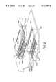
- FIG. 1shows an exploded component view of a first embodiment of the new circuit board assembly
- a laminar printed circuit board 101is equipped with at least one conductive mounting pad array 102 .
- the arrayis arranged in two parallel rows.
- the mounting padsare coupled to conductive traces (not shown) which are routed through various levels in the board.
- Each mounting pad 103 within array 102has an inner portion 103 A and an outer portion 103 B. It will be noted that the inner and outer portions of the next to the last pad 103 C on the left row of array 102 are insulated from one another to provide independent chip select signals on each pad portion.
- This viewshows a first IC package 104 L is positioned directly above the mounting pad array 102 .
- An IC package carrier I Osis positioned above the first IC package 104 L.
- a second IC package 104 Uidentical to IC package 104 L, is positioned above the carrier 105 .
- Both IC packages 104 L and 104 Uare of the TSOP (Thin Small Outline Package). It should be noted that hereafter, that sub-components of IC package 104 L will be labeled with an item number followed by the letter “L”, while sub-components of IC package 104 U will be labeled with an item number followed by the letter “U”. Still referring to FIG. 1, each IC package 104 L and 104 U has a package body 106 L and 106 U made of injection-molded plastic material in which is embedded an IC chip (not shown).
- Each package 104 L and 104 Uhas a plurality of leads 107 L and 107 U.
- An upper end of each lead 104 L and 104 Uis embedded in the package body 106 L and 106 U, respectively.
- the embedded end of each leadis coupled to a single bonding pad on the embedded IC chip via one of many available processes such as wire-bonding or ball-bonding.
- Each exposed end of the leads 107 L of the lower IC package 104 Lis aligned with the inner portion 103 A of a mounting pad 103 .
- the package carrier 105has a carrier body 108 , a plurality of carrier leads 109 , and an array of carrier mounting pads 110 on an upper surface 111 of the carrier body 108 .
- the upper surface 111also incorporates two pair of decoupling capacitor bonding pads 112 A and 112 B.
- a decoupling capacitor 113will be conductively attached to each pair.
- Each carrier lead 109is coupled to a single carrier mounting pad 110 .
- the carrier 105may be fabricated in the same manner used to fabricate plastic encapsulated packages. That is, all interior ends of the carrier leads 109 are embedded within the carrier body 108 . The exterior ends of the leads 109 are attached to a lead frame.
- the frameis removed, thereby singulating and bending each of the leads 109 into the proper final shape.
- the carrier 105is equipped with a stand-off tower 114 at each corner.
- One or more conductive layers 115which may be a metal such as copper or aluminum, may be held at any potential for impedance control of the active signals of ground. Impedance control may be achieved using either stripline or microstrip structures.
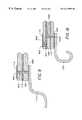
- the circuit board assembly fabrication processis most easily accomplished in a multi-step process.
- the lower IC package 104 Lis mounted on the circuit board 101 and the upper IC package and the decoupling capacitors 113 are mounted on the carrier 105 .
- FIG. 2depicts this stage of component assembly.
- the package-laden carrieris mounted on the circuit board on top of the lower IC package 104 L.
- FIG. 3depicts this final stage of component assembly.
- the leads 107 L off lower IC package 104 Lhave been conductively bonded (e.g., via soldering) to the inner portions 103 A of the bonding pads 103 of bonding pad array 102 .
- the leads 107 U of upper IC package 104 Uhave been conductively bonded to the carrier mounting pads 110 on the upper surface 111 of carrier body 108
- the decoupling capacitors 113have been conductively bonded to the capacitor bonding pads 112 A and 112 B.
- each of the carrier leads 109has been conductively bonded (via soldering or conductive epoxy, for example) to the outer portion 103 B of a bonding pad 103 of bonding pad array 102 .
- each stand-off tower 114is sized so that its base mount flush against the upper surface of the circuit board 101 when the carrier leads 109 are soldered to the bonding pads 103 .
- two IC packagesare now mounted on the circuit board 101 using only slightly more board real estate than that required for a single IC package.
- the lower and upper IC packagesare identical IC memory packages such as synchronous dynamic random access memory (SDRAM), conventional dynamic random access memory (DRAM), or static random access memory
- SDRAMsynchronous dynamic random access memory
- DRAMconventional dynamic random access memory
- static random access memorythe different chip select signals on the inner and outer portions of bonding pad 103 C provide each, of the packages to be accessed individually.
- this variant of the first embodiment circuit board assembly of FIG. 1lacks the stand-off towers 114 . It relies only on the carrier leads 109 for support.
- FIG. 5shows the module of FIG. 5 in a fully assembled state.
- FIGS. 7 through 10show various carrier designs.
- the carrier portions of FIGS. 7 and 8have embedded leads, while those of FIGS. 9 and 10 have leads attached, to a mounting pad.
- FIG. 7shows an S-shaped carrier lead 109 which is embedded within a carrier body 108 , which may be fabricated from injection molded plastic material.
- a laminar carrier mounting pad 110which attached to the carrier body 108 , is directly coupled to the lead 109 via a hole 701 , which has been plated with a conductive material 702 such as copper.
- the copper platingmakes electrical contact with both the lead 109 and the mounting pad 110 .
- Conductive layer 115is visible in this view.
- a conductive routing layer 801from which conductive traces are formed, provides indirect contact with the mounting pad 110 .
- the mounting pad 110is coupled directly to the routing conductive layer 801 via a first hole 802 plated with conductive material 803 .
- the routing conductive layer 801is, in turn, coupled directly to a J-shaped lead 502 via a second hole 804 plated with conductive material 805 .
- Conductive layer 115is also visible in this view.
- a carrier lead 110is conductively bonded (e.g., with solder or with a powdered metal filled epoxy) to a lower carrier mounting pad 902 . Electrical contact is made to a carrier mounting pad 110 , to which a lead of an IC package will be conductively bonded, via a conductively plated hole 903 plated with a conductive material 904 . It will be noted that conductive material 904 is insulated from conductive layer 115 , which is embedded within the carrier body 108 .
- electrical connectionis made between a carrier mounting pad 110 and a conductive routing layer 801 via a first hole 802 plated with conductive material 803 .
- Electrical connectionis made between the routing layer 801 and a lower carrier mounting pad 902 via a second hole 1002 that is also plated with conductive material 1003 .
- conductive material 1003is insulated from conductive layer 115 .
- the leads of surface mount IC packagesmay vary. Two types of leads are most commonly used for surface mount components. One lead is “J”-shaped; the other is “S”-shaped. The “S”-shaped leads are becoming increasingly widespread. Other types of leads for surface-mount components may also be developed. The invention should not be considered limited by the type of leads which are utilized on any of the constituent components. Lead types may also be mixed between components comprising an assembly. Thus, assemblies having a number of different lead combinations are possible. At one end of the spectrum, both packages and the carrier may utilize “J”-shaped leads. At the other end, all components will use “S”-shaped leads. Between those two extremes, each of the components may utilize either of the two leads currently available for surface-mount components.
Landscapes
- Engineering & Computer Science (AREA)
- Microelectronics & Electronic Packaging (AREA)
- Power Engineering (AREA)
- Physics & Mathematics (AREA)
- Condensed Matter Physics & Semiconductors (AREA)
- General Physics & Mathematics (AREA)
- Computer Hardware Design (AREA)
- Manufacturing & Machinery (AREA)
- Structures For Mounting Electric Components On Printed Circuit Boards (AREA)
Abstract
Description
This invention relates to the production of circuit board assemblies and electronic modules, such as memory modules, and more particularly to a method and apparatus for attaching integrated circuit packages to printed circuit boards. It also relates to high-density memory modules having three-dimensional arrangements of integrated circuit packages.
Demand for semiconductor memory is highly elastic. When such memory is relatively inexpensive compared to the overall cost of a computer system, an almost unsatiable demand results, with computer manufacturers tending to install an amount of main memory in each system that greatly exceeds the amount required for average program use. On the other hand, when it is costly, manufacturers typically install an amount in each system that only marginally fulfills the requirement of the average program. Although the sales prices of computers may, thus, be maintained at low levels, the end user may soon find that he must upgrade his computer's main memory.
The ever increasing demand for large random access computer memories, and the growing demand for increasingly compact computers, coupled with an incentive on the part of the semiconductor manufactureres to reduce the cost per bit, has lead to not only a quadrupling of circuit density approximately every three years, but to increasingly efficient techniques for packaging and mounting the circuit chips. Up until the late 1980's, semiconductor memory chips were usually packaged as dual in-line pin packages (DIPPs). The pins of these DIPP packages were generally soldered directly within through-holes in a main circuit board (e.g., the motherboard), or they were inserted in sockets which were, in turn, soldered within through-holes in the main circuit board. With the advent of surface mount technology, conventional plated through-holes on printed circuit boards have been replace with conductive mounting pads. Small Outline J-lead (SOJ) packages have lead to Thin Small Outline Packages (TSOPs). Because the pitch or spacing between centers of adjacent surface mount pins is significantly less than the conventional 0.10-inch spacing for conventional through-hole components, surface mount chips tend to be considerably smaller than corresponding conventional chips, thus taking up less space on a printed circuit board. Additionally, as through holes are no longer needed, surface mount technology lends itself to the mounting of components on both sides of a printed circuit board. Memory modules utilizing surface-mount packages on both sides have become the standard. Both the earlier single in-line memory modules (SIMMs) and the currently used dual in-line memory modules (DIMMs) are inserted into sockets on the motherboard.
Packaging density may be increased rather dramatically fabricating modules in which a plurality of integrated circuit (IC) chips, such as memory chips, are stacked in a three dimensional arrangement. As a general rule, the three-dimensional stacking of chips requires complex, non-standard packaging methods.
One example of a vertical stack of IC chips is provided by U.S. Pat. No. 4,956,694 to Floyd Eide, titled INTEGRATED CIRCUIT CHIP STACKING. A plurality of integrated circuits are packaged within chip carriers and stacked, one on top of the other, on a printed circuit board. Except for the chip select terminal, all other like terminals on the chips are connected in parallel.
Another example of chip stacking is given in U.S. Pat. No. 5,128,831 to Fox, et al. titled HIGH-DENSITY ELECTRONIC PACKAGE COMPRISING STACKED SUB-MODULES WHICH ARE ELECTRICALLY INTERCONNECTED BY SOLDER-FILLED VIAS. The package is assembled from individually testable sub-modules, each of which has a single chip bonded thereto. The sub-modules are interleaved with frame-like spacers. Both the sub-modules and the spacers have alignable vias which provide interconnection between the various sub-modules.
U.S. Pat. No. 5,313,096, also issued to Floyd Eide and titled IC CHIP PACKAGE HAVING CHIP ATTACHED TO AND WIRE BONDED WITHIN AN OVERLYING SUBSTRATE, is another example. Such a package includes a chip having an upper active surface bonded to the lower surface of a lower substrate layer having conductive traces on its upper surface which terminate in conductive pads on its periphery. Connection between terminals on the active surface and the traces is made with wire bonds through apertures within the lower substrate layer. An upper substrate layer, which is bonded to the lower substrate layer, has apertures which coincide with those of the lower substrate layer and provide space in which the wire bonding may occur. After wire bonding has occurred, the apertures are filled with epoxy to form an individually testable sub-module. Multiple sub-modules can be stacked and interconnected with metal strips attached to their edges.
A final example of a stacked-chip module is disclosed in U.S. Pat. No. 5,869,353 to A. U. Levy, et al. titled MODULAR PANEL STACKING PROCESS. A plurality of panels are fabricated having apertures therein, an array of chip-mounting pads at the bottom of the apertures, and interfacing conductive pads. Both the chip-mounting pads and the interfacing conductive pads are coated with solder paste. Plastic-encapsulated surface-mount IC chips are positioned on the paste-covered mounting pads, multiple panels are stacked in a layered arrangement and the stack is heated to solder the chip leads to the mounting pads and the interfacing pads of adjacent panels together. Individual chip package stacks are then separated from the panel stack by a cutting and cleaving operation.
As can be seen by the foregoing examples, increased chip density is achieved through the use of complicated packaging and stacking arrangements, which must necessarily be reflected in a higher costs per bit of storage.
The present invention provides for an improved circuit board assembly having increased chip density. A preferred embodiment of the improved assembly is fabricated with standard plastic-encapsulated, surface-mount IC chips using conventional circuit board assembly techniques. The assembly includes a printed circuit board having at least one primary mounting pad array affixed thereto, each pad of said primary array having first and second portions; a first integrated circuit (IC) package having a package body and a plurality of primary leads attached to the package body, each of which is conductively bonded to the first portion of a different mounting pad of said primary array; a package carrier positioned above the first IC package, the carrier having a carrier body with a package mounting surface thereon, a plurality of carrier leads attached to the carrier body, and a secondary mounting pad array affixed to the package mounting surface, each carrier lead being coupled to a different pad of said secondary mounting pad array, each carrier lead being conductively bonded to the second portion of a different mounting pad of said primary array; and a second integrated circuit package having a plurality of secondary leads, each of which is conductively bonded to a different mounting pad of said secondary array. The first and second IC packages are of identical shape and configuration.
The invention may be utilized to increase memory density on memory modules. For other types of IC packages, it may be employed to more efficiently utilize available real estate on a printed circuit board. In the case of packages containing memory chips, each lead, with the exception of chip select leads, is directly coupled to a corresponding lead on the other package. In order maintain chip select signals separate for each package, the first and second portions of the chip select pad on the first array are not coextensive, but rather are insulated from one another.
Variations of both basic embodiments are possible. For example, the leads of surface mount IC packages may vary. Two types of leads are most commonly used for surface mount components. One lead is “J”-shaped; the other is “S”-shaped. The “S”-shaped leads are becoming increasingly widespread. Other types of leads for surface-mount components may also be developed. The invention should not be considered limited by the type of leads which are utilized on any of the constituent components. Lead types may also be mixed between components. Thus, assemblies having a number of different lead combinations are possible. At one end of the spectrum, both packages and the carrier may utilize “J”-shaped leads. At the other end, all components will use “S”-shaped leads. Between those two extremes, each of the components may utilize either of the two leads currently available for surface-mount components.
FIG. 1 is an exploded isometric view of a first embodiment of the new multi-chip module in which the carrier has standoffs and both IC packages and the package carrier have “S”-shaped leads;
FIG. 2 is an isometric partially-assembled view of the first embodiment of the multi-chip module of FIG. 1;
FIG. 3 is an isometric fully-assembled view of the first embodiment of the multi-chip module of FIG. 1;
FIG. 4 is an exploded isometric view of a variant of the first embodiment of the new multi-chip module, employing a package carrier having no standoffs;
FIG. 5 is an exploded isometric view of a first embodiment of the new multi-chip module in which both IC packages have “S”-shaped leads and the package carrier has “J”-shaped leads;
FIG. 6 is an isometric assembled view of the first embodiment of the multi-chip module of FIG. 5;
FIG. 7 is a cross-sectional view through a single embedded lead of a carrier in which direct connection is made between a carrier mounting pad and the lead;
FIG. 8 is a cross-sectional view through a single embedded lead of a carrier in which indirect connection is made between a carrier mounting pad and the lead;
FIG. 9 is a cross-sectional view through a single attached lead of a carrier in which direct connection is made between a carrier mounting pad and the lead; and
FIG. 10 is a cross-sectional view through a single attached lead of a carrier in which indirect connection is made between a carrier mounting pad and the lead.
As will be evident from the attached drawing figures, the present invention permits the manufacture of circuit board assemblies having increased circuit density. The invention may be used for a variety of applications. One very obvious usage is in the manufacture of memory modules. As memory modules typically incorporate a printed circuit board having rigidly prescribed dimensions, more efficient use of the board real estate will result in a module having greater total memory capacity. The invention may also be utilized to closely couple related, but dissimilar, IC packages. For example, it may be desirable to mount an IC package containing high-speed cache memory on top of an IC package containing a microprocessor chip. The various embodiments of the improved circuit board assembly will now be described in detail with reference to the accompanying drawings.
Referring now to FIG. 1, which shows an exploded component view of a first embodiment of the new circuit board assembly, a laminar printedcircuit board 101 is equipped with at least one conductivemounting pad array 102. In this case, the array is arranged in two parallel rows. As with conventional circuit board design, the mounting pads are coupled to conductive traces (not shown) which are routed through various levels in the board. Each mountingpad 103 withinarray 102 has aninner portion 103A and anouter portion 103B. It will be noted that the inner and outer portions of the next to thelast pad 103C on the left row ofarray 102 are insulated from one another to provide independent chip select signals on each pad portion. This view shows afirst IC package 104L is positioned directly above the mountingpad array 102. An IC package carrier I Os is positioned above thefirst IC package 104L. Asecond IC package 104U, identical toIC package 104L, is positioned above thecarrier 105. Both IC packages104L and104U are of the TSOP (Thin Small Outline Package). It should be noted that hereafter, that sub-components ofIC package 104L will be labeled with an item number followed by the letter “L”, while sub-components ofIC package 104U will be labeled with an item number followed by the letter “U”. Still referring to FIG. 1, eachIC package package body package leads package body leads 107L of thelower IC package 104L is aligned with theinner portion 103A of amounting pad 103.
Still referring to FIG. 1 thepackage carrier 105 has acarrier body 108, a plurality of carrier leads109, and an array ofcarrier mounting pads 110 on anupper surface 111 of thecarrier body 108. Theupper surface 111 also incorporates two pair of decouplingcapacitor bonding pads decoupling capacitor 113 will be conductively attached to each pair. Eachcarrier lead 109 is coupled to a singlecarrier mounting pad 110. Thecarrier 105 may be fabricated in the same manner used to fabricate plastic encapsulated packages. That is, all interior ends of the carrier leads109 are embedded within thecarrier body 108. The exterior ends of theleads 109 are attached to a lead frame. During a trim and form operation, the frame is removed, thereby singulating and bending each of theleads 109 into the proper final shape. It will be noted that thecarrier 105 is equipped with a stand-off tower 114 at each corner. One or moreconductive layers 115, which may be a metal such as copper or aluminum, may be held at any potential for impedance control of the active signals of ground. Impedance control may be achieved using either stripline or microstrip structures.
The circuit board assembly fabrication process is most easily accomplished in a multi-step process. Thelower IC package 104L is mounted on thecircuit board 101 and the upper IC package and thedecoupling capacitors 113 are mounted on thecarrier 105. FIG. 2 depicts this stage of component assembly. Finally, the package-laden carrier is mounted on the circuit board on top of thelower IC package 104L. FIG. 3 depicts this final stage of component assembly. Referring now to FIG. 2, theleads 107L offlower IC package 104L have been conductively bonded (e.g., via soldering) to theinner portions 103A of thebonding pads 103 ofbonding pad array 102. Likewise, theleads 107U ofupper IC package 104U have been conductively bonded to thecarrier mounting pads 110 on theupper surface 111 ofcarrier body 108, and thedecoupling capacitors 113 have been conductively bonded to thecapacitor bonding pads
Referring now to FIG. 3, each of the carrier leads109 has been conductively bonded (via soldering or conductive epoxy, for example) to theouter portion 103B of abonding pad 103 ofbonding pad array 102. It will be noted that each stand-off tower 114 is sized so that its base mount flush against the upper surface of thecircuit board 101 when the carrier leads109 are soldered to thebonding pads 103. For this embodiment of the carrier, it will also be noted that two IC packages are now mounted on thecircuit board 101 using only slightly more board real estate than that required for a single IC package. If the lower and upper IC packages (104L and104U, respectively) are identical IC memory packages such as synchronous dynamic random access memory (SDRAM), conventional dynamic random access memory (DRAM), or static random access memory, the different chip select signals on the inner and outer portions ofbonding pad 103C provide each, of the packages to be accessed individually.
Referring now to the exploded view of FIG. 4, this variant of the first embodiment circuit board assembly of FIG. 1 lacks the stand-offtowers 114. It relies only on the carrier leads109 for support.
Referring now to the exploded view of FIG. 5, another variant of the first embodiment of the new circuit board assembly is similar in most respects to the assembly of FIGS. 1,2 and3. The primary difference is thepackage carrier 501, which is equipped with “J”-shapedleads 502, rather than with “S”-shapedleads 109, as onpackage carrier 105. The “J”-shaped leads allow a slightly narrower mounting footprint for thepackage carrier 501, as the solderable portion of each lead curves inwardly (i.e., toward the package body), rather than outwardly (i.e., away from the package body). This means that theouter portion 103B of each mounting pad503 of mounting pad array504 may be somewhat shorter than the mountingpad array 102 of FIGS. 1,2 and3. In all other respects the two assemblies are identical. Therefore, identical items of the two modules share identical item numbers. FIG. 6 shows the module of FIG. 5 in a fully assembled state.
FIGS. 7 through 10 show various carrier designs. The carrier portions of FIGS. 7 and 8 have embedded leads, while those of FIGS. 9 and 10 have leads attached, to a mounting pad. FIG. 7 shows an S-shapedcarrier lead 109 which is embedded within acarrier body 108, which may be fabricated from injection molded plastic material. A laminarcarrier mounting pad 110, which attached to thecarrier body 108, is directly coupled to thelead 109 via ahole 701, which has been plated with aconductive material 702 such as copper. The copper plating makes electrical contact with both thelead 109 and the mountingpad 110.Conductive layer 115 is visible in this view.
In FIG. 8, aconductive routing layer 801, from which conductive traces are formed, provides indirect contact with the mountingpad 110. In this case, the mountingpad 110 is coupled directly to the routingconductive layer 801 via afirst hole 802 plated withconductive material 803. The routingconductive layer 801 is, in turn, coupled directly to a J-shapedlead 502 via asecond hole 804 plated withconductive material 805.Conductive layer 115 is also visible in this view.
Referring now to FIG. 9, acarrier lead 110 is conductively bonded (e.g., with solder or with a powdered metal filled epoxy) to a lowercarrier mounting pad 902. Electrical contact is made to acarrier mounting pad 110, to which a lead of an IC package will be conductively bonded, via a conductively platedhole 903 plated with aconductive material 904. It will be noted thatconductive material 904 is insulated fromconductive layer 115, which is embedded within thecarrier body 108.
Referring now to FIG. 10, electrical connection is made between acarrier mounting pad 110 and aconductive routing layer 801 via afirst hole 802 plated withconductive material 803. Electrical connection is made between therouting layer 801 and a lowercarrier mounting pad 902 via asecond hole 1002 that is also plated withconductive material 1003. It will be noted thatconductive material 1003 is insulated fromconductive layer 115.
Although only several single embodiments of the invention have been heretofore described, it will be obvious to those having ordinary skill in the art that changes and modifications may be made thereto without departing from the scope and the spirit of the invention as hereinafter claimed. For example, many variations of two basic embodiments are possible. For example, the leads of surface mount IC packages may vary. Two types of leads are most commonly used for surface mount components. One lead is “J”-shaped; the other is “S”-shaped. The “S”-shaped leads are becoming increasingly widespread. Other types of leads for surface-mount components may also be developed. The invention should not be considered limited by the type of leads which are utilized on any of the constituent components. Lead types may also be mixed between components comprising an assembly. Thus, assemblies having a number of different lead combinations are possible. At one end of the spectrum, both packages and the carrier may utilize “J”-shaped leads. At the other end, all components will use “S”-shaped leads. Between those two extremes, each of the components may utilize either of the two leads currently available for surface-mount components.
Claims (34)
1. A circuit board assembly comprising:
a printed circuit board having at least one principal mounting pad array affixed thereto, each pad of said array having first and second portions, not more than one of said principal mounting pads having noncontiguous first and second portions;
a first integrated circuit package having a plurality of primary leads, each of which is conductively bonded to the first portion of a different mounting pad of said array;
a package carrier having a plurality of carrier leads, each of which is conductively bonded to the second portion of a different mounting pad of said principal mounting pad array, said carrier having an auxilliary mounting pad array thereon, wherein each auxilliary mounting pad can be coupled to a different carrier lead;
a second integrated circuit package having a plurality of secondary leads, each of which is conductively bonded to a corresponding auxilliary mounting pad of said auxilliary mounting pad array; and
means for selecting between said first and second integrated circuit packages.
2. The circuit board assembly of claim1, wherein said first and second integrated circuit packages are identically configured with respect to lead position and function, and wherein corresponding leads of said first and second packages are, generally, electrically coupled to first and second portions, respectively, of the same mounting pads.
3. The circuit board assembly of claim2, wherein said means of selecting comprises one principal mounting pad having non-contiguous, dielectrically-insulated first and second portions, each portion receiving a different chip select signal for each of said first and second integrated circuit packages.
4. The circuit board assembly of claim1, wherein both first and second packages are of the TSOP type.
5. The circuit board assembly of claim1, wherein both first and second packages are of the SOJ type.
6. The circuit board assembly of claim1, wherein said first and second packages are of dissimilar types, being selected from the group consisting of TSOP and SOJ types.
7. The circuit board assembly of claim1, wherein said carrier leads and said auxilliary mounting pads are formed from lead frame elements which are partially embedded within said package carrier.
8. The circuit board assembly of claim1, wherein said carrier is positioned above said first integrated circuit package, and said second integrated circuit package is positioned on an upper surface of said carrier.
9. The circuit board assembly of claim1, wherein said means for selecting comprises a rerouting of signal inputs to the second integrated circuit package via a routing layer in said package carrier.
10. A circuit board assembly comprising:
a printed circuit board having at least one primary mounting pad array affixed thereto, each pad of said primary array having first and second portions, not more than one of said primary mounting pads having noncontiguous first and second portions;
a first integrated circuit package having a plurality of primary leads, each of which is attached to the first portion of a different mounting pad of said primary array;
a package carrier having a plurality of carrier leads attached thereto and a package mounting surface thereon, said package mounting surface having a secondary mounting pad array attached thereto, wherein each pad of the secondary mounting pad array can be coupled to at least one carrier lead, each carrier lead being attached to the second portion of a different mounting pad of said primary array;
a second integrated circuit package having a plurality of secondary leads, each of which is attached to a different mounting pad of said secondary array; and
means for selecting between said first and second integrated circuit packages.
11. The circuit board assembly of claim10, wherein said first and second integrated circuit packages are identically configured with respect to lead position and function, and wherein corresponding leads of said first and second packages are, generally, electrically coupled to first and second portions, respectively, of the same primary bonding pads.
12. The circuit board assembly of claim11, wherein said means of selecting comprises one primary mounting pad having non-contiguous, dielectrically-insulated first and second portions, each portion receiving a different chip select signal.
13. The circuit board assembly of claim10, wherein both first and second integrated circuit packages are of the TSOP type.
14. The circuit board assembly of claim10, wherein both first and second integrated circuit packages are of the SOJ type.
15. The circuit board assembly of claim10, wherein said first and second integrated circuit packages have leads of dissimilar types.
16. The circuit board assembly of claim10, wherein said carrier leads and said secondary mounting pads are formed from lead frame elements which are partially embedded within said package carrier.
17. The circuit board assembly of claim10, wherein said carrier body is positioned above said first integrated circuit package, and said second integrated circuit package is positioned on an upper surface of said carrier body.
18. The circuit board assembly of claim10, wherein said means for selecting comprises a rerouting of signal inputs to the second integrated circuit package via a routing layer in said package carrier.
19. A circuit board assembly comprising:
a printed circuit board having at least one primary mounting pad array affixed thereto, said primary array having a center point, each pad of said primary array having inner and outer portions, the inner portion of each pad being nearer said center point than the outer portion of the same pad, not more than one of said primary mounting pads having noncontiguous first and second portions;
a first integrated circuit package having a plurality of primary leads, each of which is conductively bonded to the inner portion of a different mounting pad of said primary array;
a package carrier having a carrier body having a package mounting surface on an upper surface thereof, said package mounting surface having a secondary mounting pad array attached thereto, said carrier body positioned above said first package, said package carrier also having a plurality of carrier leads attached to said carrier body, wherein each carrier lead can be coupled to a different pad of said secondary mounting pad array, each carrier lead being conductively bonded to the outer portion of a different mounting pad of said primary array;
a second integrated circuit package having a plurality of secondary leads, each of which is conductively bonded to a different mounting pad of said secondary array; and
means for selecting between said first and second integrated circuit packages.
20. The circuit board assembly of claim19, wherein said first and second integrated circuit packages are identically configured with respect to lead position and function, and wherein corresponding leads of said first and second packages are, generally, electrically coupled to first and second portions, respectively, of the same primary bonding pads.
21. The circuit board assembly of claim20, wherein said means of selecting comprises one primary mounting pad having dielectrically insulated first and second portions, each portion receiving a different chip select signal for each of said first and second integrated circuit packages.
22. The circuit board assembly of claim19, wherein said carrier leads and said secondary mounting pads are formed from lead frame elements which are partially embedded within said package carrier body.
23. The circuit board assembly of claim19, wherein said means for selecting comprises a rerouting of signal inputs to the second integrated circuit package via a routing layer in said package carrier.
24. A circuit board assembly comprising:
a printed circuit board having at least one primary mounting pad array affixed thereto, each array having at least first and second parallel rows of spaced-apart primary mounting pads, each primary mounting pad having inner and outer portions, not more than one of said primary mounting pads having noncontiguous inner and outer portions;
a first integrated circuit package having a first package body in which is embedded a first integrated circuit chip, at least first and second parallel rows of primary electrical leads, each lead having an exposed first portion and a second portion embedded within said first body and electrically interconnected to said first integrated circuit chip, each lead of said first row of primary leads being conductively bonded to the inner portion of a different mounting pad within said first row of primary mounting pads, each lead of said second row of primary leads being conductively bonded to the inner portion of a different mounting pad within said second row of primary mounting pads;
a package carrier having a carrier body having a package mounting surface, first and second parallel rows of carrier electrical leads attached to said carrier body, each lead of said first row of carrier leads being conductively bonded to the outer portion of a different mounting pad within said first row of primary mounting pads, each lead of said second row of leads being conductively bonded to the outer portion of a different mounting pad within said second row of primary mounting pads, said package carrier also having a secondary mounting pad array affixed to said package-mounting surface, said secondary array having at least first and second parallel rows of spaced-apart secondary mounting pads, wherein each secondary mounting pad can be electrically coupled to a different carrier lead;
second integrated circuit package having a second package body in which is embedded a second integrated circuit chip, at least first and second parallel rows of secondary electrical leads, each lead having an exposed first portion and a second portion embedded within said second body and electrically interconnected to said second integrated circuit chip, each lead of said first row of secondary leads being conductively bonded to a different pad of said first row of said secondary mounting pads, each lead of said second row of secondary leads being conductively bonded to a different pad of said second row said secondary mounting pads; and
means for selecting between said first and second integrated circuit packages.
25. The circuit board assembly of claim24, wherein said first and second integrated circuit packages are identically configured with respect to lead position and function, and wherein corresponding leads of said first and second packages are, generally, electrically coupled to inner and outer portions, respectively, of the same primary bonding pads.
26. The circuit board assembly of claim25, wherein said means of selecting comprises one primary mounting pad having noncontiguous, dielectrically-insulated inner and outer portions, each portion receiving a different chip select signal for each of said first and second integrated circuit packages.
27. The circuit board assembly of claim26, wherein dielectrically insulated inner and outer portions of a single primary mounting pad provide separate chip select signals for said first and second integrated circuit packages.
28. The circuit board assembly of claim24, wherein both first and second packages are of the TSOP type.
29. The circuit board assembly of claim24, wherein both first and second packages are of the SOJ type.
30. The circuit board assembly of claim24, wherein said first and second packages are of dissimilar types, being selected from the group consisting of TSOP and SOJ types.
31. The circuit board assembly of claim24, wherein said carrier leads and said secondary mounting pads are formed from lead frame members which are partially embedded within said carrier body.
32. The circuit board assembly of claim24, wherein said carrier body is positioned above said first integrated circuit package, and said second integrated circuit package is positioned on an upper surface of said carrier body.
33. The circuit board assembly of claim24, which further comprises: third and fourth mutually parallel rows of spaced-apart primary mounting pads affixed to said circuit board, said third and fourth rows being perpendicular to said first and second rows, each primary mounting pad within said third and fourth rows having inner and outer portions;
third and fourth parallel rows of primary electrical leads, said third and fourth rows of primary electrical leads being perpendicular to said first and second rows of primary electrical leads, each lead within said third and fourth rows of primary electrical leads having an exposed first portion and a second portion embedded within said first body and electrically interconnected to said first integrated circuit chip, each lead of said third row of primary leads being conductively bonded to the inner portion of a different mounting pad within said third row of primary mounting pads, each lead of said fourth row of primary leads being conductively bonded to a the inner portion of a different mounting pad within said fourth row of primary mounting pads;
third and fourth parallel rows of carrier electrical leads attached to said carrier body, each lead of said third row of carrier leads being conductively bonded to the outer portion of a different mounting pad within said third row of primary mounting pads, each lead of said fourth row of leads being conductively bonded to the outer portion of a different mounting pad within said fourth row of primary mounting pads;
third and fourth parallel rows of spaced-apart secondary mounting pads on said secondary mounting pad array, wherein each secondary mounting pad of said first, second, third and fourth rows can be electrically coupled to a different carrier lead; and
third and fourth parallel rows of secondary electrical leads, each such lead having an exposed first portion and a second portion embedded within said second body and electrically interconnected to said second integrated circuit chip, each lead of said third row of secondary leads being conductively bonded to a different pad of said third row of said secondary mounting pads, each lead of said fourth row of secondary leads being conductively bonded to a different pad of said fourth row of said secondary mounting pads.
34. The circuit board assembly of claim24, wherein said means for selecting comprises a rerouting of signal inputs to the second integrated circuit package via a routing layer in said package carrier.
Priority Applications (1)
| Application Number | Priority Date | Filing Date | Title |
|---|---|---|---|
| US09/285,354US6313998B1 (en) | 1999-04-02 | 1999-04-02 | Circuit board assembly having a three dimensional array of integrated circuit packages |
Applications Claiming Priority (1)
| Application Number | Priority Date | Filing Date | Title |
|---|---|---|---|
| US09/285,354US6313998B1 (en) | 1999-04-02 | 1999-04-02 | Circuit board assembly having a three dimensional array of integrated circuit packages |
Publications (1)
| Publication Number | Publication Date |
|---|---|
| US6313998B1true US6313998B1 (en) | 2001-11-06 |
Family
ID=23093873
Family Applications (1)
| Application Number | Title | Priority Date | Filing Date |
|---|---|---|---|
| US09/285,354Expired - LifetimeUS6313998B1 (en) | 1999-04-02 | 1999-04-02 | Circuit board assembly having a three dimensional array of integrated circuit packages |
Country Status (1)
| Country | Link |
|---|---|
| US (1) | US6313998B1 (en) |
Cited By (50)
| Publication number | Priority date | Publication date | Assignee | Title |
|---|---|---|---|---|
| US20020167802A1 (en)* | 2001-04-24 | 2002-11-14 | Kozo Wada | Printed circuit board |
| US6501664B1 (en)* | 2000-06-30 | 2002-12-31 | Intel Corporation | Decoupling structure and method for printed circuit board component |
| US6542393B1 (en) | 2002-04-24 | 2003-04-01 | Ma Laboratories, Inc. | Dual-bank memory module with stacked DRAM chips having a concave-shaped re-route PCB in-between |
| US6572387B2 (en) | 1999-09-24 | 2003-06-03 | Staktek Group, L.P. | Flexible circuit connector for stacked chip module |
| WO2003058719A1 (en)* | 2002-01-11 | 2003-07-17 | Societe Novatec | Monolithic interconnection interface for the stacking of electronic components and the production method thereof |
| US6611434B1 (en)* | 2000-10-30 | 2003-08-26 | Siliconware Precision Industries Co., Ltd. | Stacked multi-chip package structure with on-chip integration of passive component |
| US20030173679A1 (en)* | 2002-03-13 | 2003-09-18 | Levardo Melvin N. | Stacked dice standoffs |
| US6643142B2 (en)* | 2000-10-11 | 2003-11-04 | Koninklijke Philips Electronics N.V. | Module having a lead frame equipped with components on both sides |
| US6717824B2 (en)* | 1999-07-09 | 2004-04-06 | Fujitsu Limited | Printed wiring board unit, auxiliary substrate for hierarchical mounting, and electronic apparatus |
| US20040108590A1 (en)* | 2000-10-16 | 2004-06-10 | Kledzik Kenneth J. | Carrier-based electronic module |
| US6801440B2 (en)* | 2001-03-14 | 2004-10-05 | Murata Manufacturing Co., Ltd. | Mounting structure for module substrates |
| US20040252474A1 (en)* | 2002-11-25 | 2004-12-16 | Kwanghak Lee | Integrated circuit stack with lead frames |
| US6873035B2 (en)* | 2000-12-15 | 2005-03-29 | Renesas Technology Corp. | Semiconductor device having capacitors for reducing power source noise |
| US6919626B2 (en) | 1992-12-11 | 2005-07-19 | Staktek Group L.P. | High density integrated circuit module |
| US7026708B2 (en) | 2001-10-26 | 2006-04-11 | Staktek Group L.P. | Low profile chip scale stacking system and method |
| US7033861B1 (en) | 2005-05-18 | 2006-04-25 | Staktek Group L.P. | Stacked module systems and method |
| US7053478B2 (en) | 2001-10-26 | 2006-05-30 | Staktek Group L.P. | Pitch change and chip scale stacking system |
| US7081373B2 (en) | 2001-12-14 | 2006-07-25 | Staktek Group, L.P. | CSP chip stack with flex circuit |
| US20060220257A1 (en)* | 2005-03-21 | 2006-10-05 | Dae-Ho Lee | Multi-chip package and method for manufacturing the same |
| US7180167B2 (en) | 2001-10-26 | 2007-02-20 | Staktek Group L. P. | Low profile stacking system and method |
| US7202555B2 (en) | 2001-10-26 | 2007-04-10 | Staktek Group L.P. | Pitch change and chip scale stacking system and method |
| US20070080470A1 (en)* | 2005-10-11 | 2007-04-12 | Staktek Group L.P. | Leaded package integrated circuit stacking |
| USRE39628E1 (en) | 1999-05-05 | 2007-05-15 | Stakick Group, L.P. | Stackable flex circuit IC package and method of making same |
| US7256484B2 (en) | 2001-10-26 | 2007-08-14 | Staktek Group L.P. | Memory expansion and chip scale stacking system and method |
| US7304382B2 (en) | 2006-01-11 | 2007-12-04 | Staktek Group L.P. | Managed memory component |
| US7309914B2 (en) | 2005-01-20 | 2007-12-18 | Staktek Group L.P. | Inverted CSP stacking system and method |
| US7310458B2 (en) | 2001-10-26 | 2007-12-18 | Staktek Group L.P. | Stacked module systems and methods |
| US20080012110A1 (en)* | 2006-07-17 | 2008-01-17 | Micron Technology, Inc. | Microelectronic packages with leadframes, including leadframes configured for stacked die packages, and associated systems and methods |
| US7335975B2 (en) | 2001-10-26 | 2008-02-26 | Staktek Group L.P. | Integrated circuit stacking system and method |
| US20080054437A1 (en)* | 2006-09-06 | 2008-03-06 | Samsung Electronics Co., Ltd. | Pop package and method of fabricating the same |
| US7371609B2 (en) | 2001-10-26 | 2008-05-13 | Staktek Group L.P. | Stacked module systems and methods |
| US7417310B2 (en) | 2006-11-02 | 2008-08-26 | Entorian Technologies, Lp | Circuit module having force resistant construction |
| US7468553B2 (en) | 2006-10-20 | 2008-12-23 | Entorian Technologies, Lp | Stackable micropackages and stacked modules |
| US7485951B2 (en) | 2001-10-26 | 2009-02-03 | Entorian Technologies, Lp | Modularized die stacking system and method |
| US20090057862A1 (en)* | 2007-08-31 | 2009-03-05 | Jong-Woo Ha | Integrated circuit package-in-package system with carrier interposer |
| US7508058B2 (en) | 2006-01-11 | 2009-03-24 | Entorian Technologies, Lp | Stacked integrated circuit module |
| US7508069B2 (en) | 2006-01-11 | 2009-03-24 | Entorian Technologies, Lp | Managed memory component |
| US7524703B2 (en) | 2001-10-26 | 2009-04-28 | Entorian Technologies, Lp | Integrated circuit stacking system and method |
| US7542304B2 (en) | 2003-09-15 | 2009-06-02 | Entorian Technologies, Lp | Memory expansion and integrated circuit stacking system and method |
| US7576995B2 (en) | 2005-11-04 | 2009-08-18 | Entorian Technologies, Lp | Flex circuit apparatus and method for adding capacitance while conserving circuit board surface area |
| US7605454B2 (en) | 2006-01-11 | 2009-10-20 | Entorian Technologies, Lp | Memory card and method for devising |
| US7608920B2 (en) | 2006-01-11 | 2009-10-27 | Entorian Technologies, Lp | Memory card and method for devising |
| USRE41039E1 (en) | 2000-01-13 | 2009-12-15 | Entorian Technologies, Lp | Stackable chip package with flex carrier |
| US7656678B2 (en) | 2001-10-26 | 2010-02-02 | Entorian Technologies, Lp | Stacked module systems |
| US7719098B2 (en) | 2001-10-26 | 2010-05-18 | Entorian Technologies Lp | Stacked modules and method |
| US20100164084A1 (en)* | 2008-12-26 | 2010-07-01 | Jun-Ho Lee | Semiconductor device and semiconductor package including the same |
| US7843050B2 (en) | 2007-07-24 | 2010-11-30 | Micron Technology, Inc. | Microelectronic die packages with metal leads, including metal leads for stacked die packages, and associated systems and methods |
| US7947529B2 (en) | 2007-08-16 | 2011-05-24 | Micron Technology, Inc. | Microelectronic die packages with leadframes, including leadframe-based interposer for stacked die packages, and associated systems and methods |
| US20130081266A1 (en)* | 2007-08-31 | 2013-04-04 | Intersil Americas LLC | Stackable electronic component |
| RU2584180C2 (en)* | 2014-07-17 | 2016-05-20 | Открытое акционерное общество "Научно-исследовательский институт электронной техники" | Method of assembling three-dimensional integrated 3d bis circuits |
Citations (12)
| Publication number | Priority date | Publication date | Assignee | Title |
|---|---|---|---|---|
| US4437235A (en)* | 1980-12-29 | 1984-03-20 | Honeywell Information Systems Inc. | Integrated circuit package |
| US4956694A (en) | 1988-11-04 | 1990-09-11 | Dense-Pac Microsystems, Inc. | Integrated circuit chip stacking |
| US5128831A (en) | 1991-10-31 | 1992-07-07 | Micron Technology, Inc. | High-density electronic package comprising stacked sub-modules which are electrically interconnected by solder-filled vias |
| US5239447A (en)* | 1991-09-13 | 1993-08-24 | International Business Machines Corporation | Stepped electronic device package |
| US5311401A (en)* | 1991-07-09 | 1994-05-10 | Hughes Aircraft Company | Stacked chip assembly and manufacturing method therefor |
| US5313096A (en) | 1992-03-16 | 1994-05-17 | Dense-Pac Microsystems, Inc. | IC chip package having chip attached to and wire bonded within an overlying substrate |
| US5742097A (en)* | 1993-04-05 | 1998-04-21 | Matsushita Electric Industrial Co., Ltd. | Multilevel semiconductor integrated circuit device |
| US5744827A (en)* | 1995-11-28 | 1998-04-28 | Samsung Electronics Co., Ltd. | Three dimensional stack package device having exposed coupling lead portions and vertical interconnection elements |
| US5754408A (en)* | 1995-11-29 | 1998-05-19 | Mitsubishi Semiconductor America, Inc. | Stackable double-density integrated circuit assemblies |
| US5869353A (en) | 1997-11-17 | 1999-02-09 | Dense-Pac Microsystems, Inc. | Modular panel stacking process |
| US6084780A (en)* | 1996-02-06 | 2000-07-04 | Kabushiki Kaisha Toshiba | Printed circuit board with high electronic component density |
| US6084293A (en)* | 1997-07-25 | 2000-07-04 | Oki Electric Industry Co., Ltd. | Stacked semiconductor device |
- 1999
- 1999-04-02USUS09/285,354patent/US6313998B1/ennot_activeExpired - Lifetime
Patent Citations (12)
| Publication number | Priority date | Publication date | Assignee | Title |
|---|---|---|---|---|
| US4437235A (en)* | 1980-12-29 | 1984-03-20 | Honeywell Information Systems Inc. | Integrated circuit package |
| US4956694A (en) | 1988-11-04 | 1990-09-11 | Dense-Pac Microsystems, Inc. | Integrated circuit chip stacking |
| US5311401A (en)* | 1991-07-09 | 1994-05-10 | Hughes Aircraft Company | Stacked chip assembly and manufacturing method therefor |
| US5239447A (en)* | 1991-09-13 | 1993-08-24 | International Business Machines Corporation | Stepped electronic device package |
| US5128831A (en) | 1991-10-31 | 1992-07-07 | Micron Technology, Inc. | High-density electronic package comprising stacked sub-modules which are electrically interconnected by solder-filled vias |
| US5313096A (en) | 1992-03-16 | 1994-05-17 | Dense-Pac Microsystems, Inc. | IC chip package having chip attached to and wire bonded within an overlying substrate |
| US5742097A (en)* | 1993-04-05 | 1998-04-21 | Matsushita Electric Industrial Co., Ltd. | Multilevel semiconductor integrated circuit device |
| US5744827A (en)* | 1995-11-28 | 1998-04-28 | Samsung Electronics Co., Ltd. | Three dimensional stack package device having exposed coupling lead portions and vertical interconnection elements |
| US5754408A (en)* | 1995-11-29 | 1998-05-19 | Mitsubishi Semiconductor America, Inc. | Stackable double-density integrated circuit assemblies |
| US6084780A (en)* | 1996-02-06 | 2000-07-04 | Kabushiki Kaisha Toshiba | Printed circuit board with high electronic component density |
| US6084293A (en)* | 1997-07-25 | 2000-07-04 | Oki Electric Industry Co., Ltd. | Stacked semiconductor device |
| US5869353A (en) | 1997-11-17 | 1999-02-09 | Dense-Pac Microsystems, Inc. | Modular panel stacking process |
Cited By (88)
| Publication number | Priority date | Publication date | Assignee | Title |
|---|---|---|---|---|
| US6919626B2 (en) | 1992-12-11 | 2005-07-19 | Staktek Group L.P. | High density integrated circuit module |
| USRE39628E1 (en) | 1999-05-05 | 2007-05-15 | Stakick Group, L.P. | Stackable flex circuit IC package and method of making same |
| US6717824B2 (en)* | 1999-07-09 | 2004-04-06 | Fujitsu Limited | Printed wiring board unit, auxiliary substrate for hierarchical mounting, and electronic apparatus |
| US6572387B2 (en) | 1999-09-24 | 2003-06-03 | Staktek Group, L.P. | Flexible circuit connector for stacked chip module |
| US7066741B2 (en) | 1999-09-24 | 2006-06-27 | Staktek Group L.P. | Flexible circuit connector for stacked chip module |
| USRE41039E1 (en) | 2000-01-13 | 2009-12-15 | Entorian Technologies, Lp | Stackable chip package with flex carrier |
| US6501664B1 (en)* | 2000-06-30 | 2002-12-31 | Intel Corporation | Decoupling structure and method for printed circuit board component |
| US6643142B2 (en)* | 2000-10-11 | 2003-11-04 | Koninklijke Philips Electronics N.V. | Module having a lead frame equipped with components on both sides |
| US7405471B2 (en)* | 2000-10-16 | 2008-07-29 | Legacy Electronics, Inc. | Carrier-based electronic module |
| US20040108590A1 (en)* | 2000-10-16 | 2004-06-10 | Kledzik Kenneth J. | Carrier-based electronic module |
| US6611434B1 (en)* | 2000-10-30 | 2003-08-26 | Siliconware Precision Industries Co., Ltd. | Stacked multi-chip package structure with on-chip integration of passive component |
| US20070205505A1 (en)* | 2000-12-15 | 2007-09-06 | Renesas Technology Corp. | Semiconductor device having capacitors for reducing power source noise |
| US7233065B2 (en) | 2000-12-15 | 2007-06-19 | Renesas Technology Corp. | Semiconductor device having capacitors for reducing power source noise |
| US6873035B2 (en)* | 2000-12-15 | 2005-03-29 | Renesas Technology Corp. | Semiconductor device having capacitors for reducing power source noise |
| US20050151252A1 (en)* | 2000-12-15 | 2005-07-14 | Renesas Technology Corp. | Semiconductor device having capacitors for reducing power source noise |
| US7319268B2 (en) | 2000-12-15 | 2008-01-15 | Renesas Technology Corp | Semiconductor device having capacitors for reducing power source noise |
| US20070023895A1 (en)* | 2000-12-15 | 2007-02-01 | Renesas Technology Corp. | Semiconductor device having capacitors for reducing power source noise |
| US6801440B2 (en)* | 2001-03-14 | 2004-10-05 | Murata Manufacturing Co., Ltd. | Mounting structure for module substrates |
| US20020167802A1 (en)* | 2001-04-24 | 2002-11-14 | Kozo Wada | Printed circuit board |
| US7586758B2 (en) | 2001-10-26 | 2009-09-08 | Entorian Technologies, Lp | Integrated circuit stacking system |
| US7053478B2 (en) | 2001-10-26 | 2006-05-30 | Staktek Group L.P. | Pitch change and chip scale stacking system |
| US7310458B2 (en) | 2001-10-26 | 2007-12-18 | Staktek Group L.P. | Stacked module systems and methods |
| US7094632B2 (en) | 2001-10-26 | 2006-08-22 | Staktek Group L.P. | Low profile chip scale stacking system and method |
| US7572671B2 (en) | 2001-10-26 | 2009-08-11 | Entorian Technologies, Lp | Stacked module systems and methods |
| US7026708B2 (en) | 2001-10-26 | 2006-04-11 | Staktek Group L.P. | Low profile chip scale stacking system and method |
| US7180167B2 (en) | 2001-10-26 | 2007-02-20 | Staktek Group L. P. | Low profile stacking system and method |
| US7524703B2 (en) | 2001-10-26 | 2009-04-28 | Entorian Technologies, Lp | Integrated circuit stacking system and method |
| US7202555B2 (en) | 2001-10-26 | 2007-04-10 | Staktek Group L.P. | Pitch change and chip scale stacking system and method |
| US7495334B2 (en) | 2001-10-26 | 2009-02-24 | Entorian Technologies, Lp | Stacking system and method |
| US7485951B2 (en) | 2001-10-26 | 2009-02-03 | Entorian Technologies, Lp | Modularized die stacking system and method |
| US7595550B2 (en) | 2001-10-26 | 2009-09-29 | Entorian Technologies, Lp | Flex-based circuit module |
| US7606048B2 (en) | 2001-10-26 | 2009-10-20 | Enthorian Technologies, LP | Integrated circuit stacking system |
| US7256484B2 (en) | 2001-10-26 | 2007-08-14 | Staktek Group L.P. | Memory expansion and chip scale stacking system and method |
| US7626273B2 (en) | 2001-10-26 | 2009-12-01 | Entorian Technologies, L.P. | Low profile stacking system and method |
| US7656678B2 (en) | 2001-10-26 | 2010-02-02 | Entorian Technologies, Lp | Stacked module systems |
| US7371609B2 (en) | 2001-10-26 | 2008-05-13 | Staktek Group L.P. | Stacked module systems and methods |
| US7335975B2 (en) | 2001-10-26 | 2008-02-26 | Staktek Group L.P. | Integrated circuit stacking system and method |
| US7719098B2 (en) | 2001-10-26 | 2010-05-18 | Entorian Technologies Lp | Stacked modules and method |
| US7081373B2 (en) | 2001-12-14 | 2006-07-25 | Staktek Group, L.P. | CSP chip stack with flex circuit |
| US7193310B2 (en) | 2001-12-14 | 2007-03-20 | Stuktek Group L.P. | Stacking system and method |
| WO2003058719A1 (en)* | 2002-01-11 | 2003-07-17 | Societe Novatec | Monolithic interconnection interface for the stacking of electronic components and the production method thereof |
| FR2834822A1 (en)* | 2002-01-11 | 2003-07-18 | Novatec Sa Soc | MONOLITHIC INTERCONNECTION INTERFACE FOR STACKING ELECTRONIC COMPONENTS |
| US6753613B2 (en)* | 2002-03-13 | 2004-06-22 | Intel Corporation | Stacked dice standoffs |
| US20030173679A1 (en)* | 2002-03-13 | 2003-09-18 | Levardo Melvin N. | Stacked dice standoffs |
| US6542393B1 (en) | 2002-04-24 | 2003-04-01 | Ma Laboratories, Inc. | Dual-bank memory module with stacked DRAM chips having a concave-shaped re-route PCB in-between |
| US20040252474A1 (en)* | 2002-11-25 | 2004-12-16 | Kwanghak Lee | Integrated circuit stack with lead frames |
| US7542304B2 (en) | 2003-09-15 | 2009-06-02 | Entorian Technologies, Lp | Memory expansion and integrated circuit stacking system and method |
| US7309914B2 (en) | 2005-01-20 | 2007-12-18 | Staktek Group L.P. | Inverted CSP stacking system and method |
| US20060220257A1 (en)* | 2005-03-21 | 2006-10-05 | Dae-Ho Lee | Multi-chip package and method for manufacturing the same |
| US7033861B1 (en) | 2005-05-18 | 2006-04-25 | Staktek Group L.P. | Stacked module systems and method |
| US7323364B2 (en) | 2005-05-18 | 2008-01-29 | Staktek Group L.P. | Stacked module systems and method |
| US20070080470A1 (en)* | 2005-10-11 | 2007-04-12 | Staktek Group L.P. | Leaded package integrated circuit stacking |
| WO2007044019A1 (en)* | 2005-10-11 | 2007-04-19 | Staktek Group L.P. | Leaded package integrated circuit stacking |
| US7259452B2 (en)* | 2005-10-11 | 2007-08-21 | Staktek Group L.P. | Leaded package integrated circuit stacking |
| US20070257349A1 (en)* | 2005-10-11 | 2007-11-08 | Staktek Group L.P. | Leaded Package Integrated Circuit Stacking |
| US7576995B2 (en) | 2005-11-04 | 2009-08-18 | Entorian Technologies, Lp | Flex circuit apparatus and method for adding capacitance while conserving circuit board surface area |
| US7508058B2 (en) | 2006-01-11 | 2009-03-24 | Entorian Technologies, Lp | Stacked integrated circuit module |
| US7605454B2 (en) | 2006-01-11 | 2009-10-20 | Entorian Technologies, Lp | Memory card and method for devising |
| US7608920B2 (en) | 2006-01-11 | 2009-10-27 | Entorian Technologies, Lp | Memory card and method for devising |
| US7508069B2 (en) | 2006-01-11 | 2009-03-24 | Entorian Technologies, Lp | Managed memory component |
| US7304382B2 (en) | 2006-01-11 | 2007-12-04 | Staktek Group L.P. | Managed memory component |
| US8869387B2 (en) | 2006-07-17 | 2014-10-28 | Micron Technology, Inc. | Methods for making microelectronic die systems |
| US7692931B2 (en)* | 2006-07-17 | 2010-04-06 | Micron Technology, Inc. | Microelectronic packages with leadframes, including leadframes configured for stacked die packages, and associated systems and methods |
| US20080012110A1 (en)* | 2006-07-17 | 2008-01-17 | Micron Technology, Inc. | Microelectronic packages with leadframes, including leadframes configured for stacked die packages, and associated systems and methods |
| US7723834B2 (en)* | 2006-09-06 | 2010-05-25 | Samsung Electronics Co., Ltd. | POP package and method of fabricating the same |
| US20080054437A1 (en)* | 2006-09-06 | 2008-03-06 | Samsung Electronics Co., Ltd. | Pop package and method of fabricating the same |
| US20100136745A1 (en)* | 2006-09-06 | 2010-06-03 | Sung-Wook Hwang | Pop package and method of fabricating the same |
| US7468553B2 (en) | 2006-10-20 | 2008-12-23 | Entorian Technologies, Lp | Stackable micropackages and stacked modules |
| US7804985B2 (en) | 2006-11-02 | 2010-09-28 | Entorian Technologies Lp | Circuit module having force resistant construction |
| US7417310B2 (en) | 2006-11-02 | 2008-08-26 | Entorian Technologies, Lp | Circuit module having force resistant construction |
| US8198720B2 (en) | 2007-07-24 | 2012-06-12 | Micron Technology, Inc. | Microelectronic die packages with metal leads, including metal leads for stacked die packages, and associated systems and methods |
| US9165910B2 (en) | 2007-07-24 | 2015-10-20 | Micron Technology, Inc. | Microelectronic die packages with metal leads, including metal leads for stacked die packages, and associated systems and methods |
| US7843050B2 (en) | 2007-07-24 | 2010-11-30 | Micron Technology, Inc. | Microelectronic die packages with metal leads, including metal leads for stacked die packages, and associated systems and methods |
| US20110068454A1 (en)* | 2007-07-24 | 2011-03-24 | Micron Technology, Inc. | Microelectronic die packages with metal leads, including metal leads for stacked die packages, and associated systems and methods |
| US10396059B2 (en) | 2007-07-24 | 2019-08-27 | Micron Technology, Inc. | Microelectronic die packages with metal leads, including metal leads for stacked die packages, and associated systems and methods |
| US10056359B2 (en) | 2007-07-24 | 2018-08-21 | Micron Technology, Inc. | Microelectronic die packages with metal leads, including metal leads for stacked die packages, and associated systems and methods |
| US9653444B2 (en) | 2007-07-24 | 2017-05-16 | Micron Technology, Inc. | Microelectronic die packages with metal leads, including metal leads for stacked die packages, and associated systems and methods |
| US8906744B2 (en) | 2007-07-24 | 2014-12-09 | Micron Technology, Inc. | Microelectronic die packages with metal leads, including metal leads for stacked die packages, and associated systems and methods |
| US8536702B2 (en) | 2007-07-24 | 2013-09-17 | Micron Technology, Inc. | Microelectronic die packages with metal leads, including metal leads for stacked die packages, and associated systems and methods |
| US8525320B2 (en) | 2007-08-16 | 2013-09-03 | Micron Technology, Inc. | Microelectronic die packages with leadframes, including leadframe-based interposer for stacked die packages, and associated systems and methods |
| US20110215453A1 (en)* | 2007-08-16 | 2011-09-08 | Micron Technology, Inc. | Microelectronic die packages with leadframes, including leadframe-based interposer for stacked die packages, and associated systems and methods |
| US7947529B2 (en) | 2007-08-16 | 2011-05-24 | Micron Technology, Inc. | Microelectronic die packages with leadframes, including leadframe-based interposer for stacked die packages, and associated systems and methods |
| US20090057862A1 (en)* | 2007-08-31 | 2009-03-05 | Jong-Woo Ha | Integrated circuit package-in-package system with carrier interposer |
| US7659609B2 (en) | 2007-08-31 | 2010-02-09 | Stats Chippac Ltd. | Integrated circuit package-in-package system with carrier interposer |
| US20130081266A1 (en)* | 2007-08-31 | 2013-04-04 | Intersil Americas LLC | Stackable electronic component |
| US20100164084A1 (en)* | 2008-12-26 | 2010-07-01 | Jun-Ho Lee | Semiconductor device and semiconductor package including the same |
| US8035194B2 (en)* | 2008-12-26 | 2011-10-11 | Hynix Semiconductor Inc. | Semiconductor device and semiconductor package including the same |
| RU2584180C2 (en)* | 2014-07-17 | 2016-05-20 | Открытое акционерное общество "Научно-исследовательский институт электронной техники" | Method of assembling three-dimensional integrated 3d bis circuits |
Similar Documents
| Publication | Publication Date | Title |
|---|---|---|
| US6313998B1 (en) | Circuit board assembly having a three dimensional array of integrated circuit packages | |
| US6487078B2 (en) | Electronic module having a three dimensional array of carrier-mounted integrated circuit packages | |
| US6713854B1 (en) | Electronic circuit module with a carrier having a mounting pad array | |
| EP1327265B1 (en) | Electronic module having canopy-type carriers | |
| USRE36916E (en) | Apparatus for stacking semiconductor chips | |
| US7821127B2 (en) | Semiconductor device package having buffered memory module and method thereof | |
| US5343075A (en) | Composite stacked semiconductor device with contact plates | |
| US4763188A (en) | Packaging system for multiple semiconductor devices | |
| US7321164B2 (en) | Stack structure with semiconductor chip embedded in carrier | |
| KR0120921B1 (en) | Semiconductor device | |
| US8344518B2 (en) | Apparatus for stacking integrated circuits | |
| US5227995A (en) | High density semiconductor memory module using split finger lead frame | |
| US6943454B1 (en) | Memory module | |
| EP0221496A2 (en) | Integrated circuit package | |
| US20030067082A1 (en) | Apparatus and methods for stacking integrated circuit devices with interconnected stacking structure | |
| KR100713898B1 (en) | Laminated package | |
| KR20080029273A (en) | Stacked Packages and High-Density Multi-Packages Using the Same | |
| JPS62104149A (en) | Integrated circuit chip module | |
| HK1057645B (en) | Electronic module having canopy-type carriers | |
| HK1055015B (en) | Electronic module having a three dimensional array of carrier-mounted integrated circuit packages | |
| KR20040046020A (en) | Stacked semiconductor package and method for fabricating the same | |
| HK1077460B (en) | A high-density circuit module | |
| HK1077460A1 (en) | A high-density circuit module |
Legal Events
| Date | Code | Title | Description |
|---|---|---|---|
| AS | Assignment | Owner name:LEGACY ELECTRONICS, INC., CALIFORNIA Free format text:ASSIGNMENT OF ASSIGNORS INTEREST;ASSIGNORS:KLEDZIK, KENNETH J.;ENGLE, JASON C.;REEL/FRAME:009884/0178 Effective date:19990401 | |
| STCF | Information on status: patent grant | Free format text:PATENTED CASE | |
| FPAY | Fee payment | Year of fee payment:4 | |
| FPAY | Fee payment | Year of fee payment:8 | |
| AS | Assignment | Owner name:LEGACY ELECTRONICS, INC., SOUTH DAKOTA Free format text:ASSIGNMENT OF ASSIGNORS INTEREST;ASSIGNOR:LEGACY ELECTRONICS, INC.;REEL/FRAME:029215/0894 Effective date:20110503 | |
| REMI | Maintenance fee reminder mailed | ||
| FPAY | Fee payment | Year of fee payment:12 | |
| SULP | Surcharge for late payment | Year of fee payment:11 | |
| AS | Assignment | Owner name:GIBRALTAR BUSINESS CAPITAL, LLC, ILLINOIS Free format text:SECURITY INTEREST;ASSIGNOR:LEGACY ELECTRONICS, INC.;REEL/FRAME:033430/0982 Effective date:20140715 |