US6313688B1 - Mixer structure and method of using same - Google Patents
Mixer structure and method of using sameDownload PDFInfo
- Publication number
- US6313688B1 US6313688B1US09/709,315US70931500AUS6313688B1US 6313688 B1US6313688 B1US 6313688B1US 70931500 AUS70931500 AUS 70931500AUS 6313688 B1US6313688 B1US 6313688B1
- Authority
- US
- United States
- Prior art keywords
- signals
- coupled
- circuit
- frequency
- input
- Prior art date
- Legal status (The legal status is an assumption and is not a legal conclusion. Google has not performed a legal analysis and makes no representation as to the accuracy of the status listed.)
- Expired - Lifetime
Links
- 238000000034methodMethods0.000titleclaimsabstractdescription13
- 238000006243chemical reactionMethods0.000claimsdescription4
- 230000009467reductionEffects0.000abstractdescription6
- 238000010586diagramMethods0.000description12
- 238000004891communicationMethods0.000description9
- 239000000758substrateSubstances0.000description9
- 238000005516engineering processMethods0.000description8
- 230000003321amplificationEffects0.000description3
- 238000003199nucleic acid amplification methodMethods0.000description3
- 239000004065semiconductorSubstances0.000description3
- 230000010354integrationEffects0.000description2
- 230000003071parasitic effectEffects0.000description2
- 238000003491arrayMethods0.000description1
- 239000003990capacitorSubstances0.000description1
- 230000008878couplingEffects0.000description1
- 238000010168coupling processMethods0.000description1
- 238000005859coupling reactionMethods0.000description1
- 230000007423decreaseEffects0.000description1
- 230000001419dependent effectEffects0.000description1
- 230000000694effectsEffects0.000description1
- 230000007246mechanismEffects0.000description1
- 238000012986modificationMethods0.000description1
- 230000004048modificationEffects0.000description1
- 230000002265preventionEffects0.000description1
Images


Classifications
- H—ELECTRICITY
- H04—ELECTRIC COMMUNICATION TECHNIQUE
- H04B—TRANSMISSION
- H04B1/00—Details of transmission systems, not covered by a single one of groups H04B3/00 - H04B13/00; Details of transmission systems not characterised by the medium used for transmission
- H04B1/38—Transceivers, i.e. devices in which transmitter and receiver form a structural unit and in which at least one part is used for functions of transmitting and receiving
- H04B1/40—Circuits
- H—ELECTRICITY
- H03—ELECTRONIC CIRCUITRY
- H03D—DEMODULATION OR TRANSFERENCE OF MODULATION FROM ONE CARRIER TO ANOTHER
- H03D7/00—Transference of modulation from one carrier to another, e.g. frequency-changing
- H03D7/14—Balanced arrangements
- H03D7/1425—Balanced arrangements with transistors
- H03D7/1441—Balanced arrangements with transistors using field-effect transistors
- H—ELECTRICITY
- H03—ELECTRONIC CIRCUITRY
- H03H—IMPEDANCE NETWORKS, e.g. RESONANT CIRCUITS; RESONATORS
- H03H11/00—Networks using active elements
- H03H11/02—Multiple-port networks
- H03H11/16—Networks for phase shifting
- H03H11/22—Networks for phase shifting providing two or more phase shifted output signals, e.g. n-phase output
- H—ELECTRICITY
- H03—ELECTRONIC CIRCUITRY
- H03K—PULSE TECHNIQUE
- H03K9/00—Demodulating pulses which have been modulated with a continuously-variable signal
- H—ELECTRICITY
- H03—ELECTRONIC CIRCUITRY
- H03L—AUTOMATIC CONTROL, STARTING, SYNCHRONISATION OR STABILISATION OF GENERATORS OF ELECTRONIC OSCILLATIONS OR PULSES
- H03L7/00—Automatic control of frequency or phase; Synchronisation
- H03L7/06—Automatic control of frequency or phase; Synchronisation using a reference signal applied to a frequency- or phase-locked loop
- H03L7/08—Details of the phase-locked loop
- H03L7/099—Details of the phase-locked loop concerning mainly the controlled oscillator of the loop
- H03L7/0995—Details of the phase-locked loop concerning mainly the controlled oscillator of the loop the oscillator comprising a ring oscillator
- H—ELECTRICITY
- H03—ELECTRONIC CIRCUITRY
- H03L—AUTOMATIC CONTROL, STARTING, SYNCHRONISATION OR STABILISATION OF GENERATORS OF ELECTRONIC OSCILLATIONS OR PULSES
- H03L7/00—Automatic control of frequency or phase; Synchronisation
- H03L7/06—Automatic control of frequency or phase; Synchronisation using a reference signal applied to a frequency- or phase-locked loop
- H03L7/16—Indirect frequency synthesis, i.e. generating a desired one of a number of predetermined frequencies using a frequency- or phase-locked loop
- H03L7/18—Indirect frequency synthesis, i.e. generating a desired one of a number of predetermined frequencies using a frequency- or phase-locked loop using a frequency divider or counter in the loop
- H03L7/197—Indirect frequency synthesis, i.e. generating a desired one of a number of predetermined frequencies using a frequency- or phase-locked loop using a frequency divider or counter in the loop a time difference being used for locking the loop, the counter counting between numbers which are variable in time or the frequency divider dividing by a factor variable in time, e.g. for obtaining fractional frequency division
- H03L7/1974—Indirect frequency synthesis, i.e. generating a desired one of a number of predetermined frequencies using a frequency- or phase-locked loop using a frequency divider or counter in the loop a time difference being used for locking the loop, the counter counting between numbers which are variable in time or the frequency divider dividing by a factor variable in time, e.g. for obtaining fractional frequency division for fractional frequency division
- H—ELECTRICITY
- H04—ELECTRIC COMMUNICATION TECHNIQUE
- H04B—TRANSMISSION
- H04B1/00—Details of transmission systems, not covered by a single one of groups H04B3/00 - H04B13/00; Details of transmission systems not characterised by the medium used for transmission
- H04B1/06—Receivers
- H04B1/16—Circuits
- H04B1/26—Circuits for superheterodyne receivers
- H04B1/28—Circuits for superheterodyne receivers the receiver comprising at least one semiconductor device having three or more electrodes
- H—ELECTRICITY
- H04—ELECTRIC COMMUNICATION TECHNIQUE
- H04B—TRANSMISSION
- H04B1/00—Details of transmission systems, not covered by a single one of groups H04B3/00 - H04B13/00; Details of transmission systems not characterised by the medium used for transmission
- H04B1/38—Transceivers, i.e. devices in which transmitter and receiver form a structural unit and in which at least one part is used for functions of transmitting and receiving
- H04B1/40—Circuits
- H04B1/403—Circuits using the same oscillator for generating both the transmitter frequency and the receiver local oscillator frequency
- H—ELECTRICITY
- H03—ELECTRONIC CIRCUITRY
- H03F—AMPLIFIERS
- H03F2200/00—Indexing scheme relating to amplifiers
- H03F2200/372—Noise reduction and elimination in amplifier
- H—ELECTRICITY
- H03—ELECTRONIC CIRCUITRY
- H03H—IMPEDANCE NETWORKS, e.g. RESONANT CIRCUITS; RESONATORS
- H03H11/00—Networks using active elements
- H03H11/02—Multiple-port networks
- H03H11/04—Frequency selective two-port networks
- H03H2011/0494—Complex filters
- H—ELECTRICITY
- H03—ELECTRONIC CIRCUITRY
- H03L—AUTOMATIC CONTROL, STARTING, SYNCHRONISATION OR STABILISATION OF GENERATORS OF ELECTRONIC OSCILLATIONS OR PULSES
- H03L7/00—Automatic control of frequency or phase; Synchronisation
- H03L7/06—Automatic control of frequency or phase; Synchronisation using a reference signal applied to a frequency- or phase-locked loop
- H03L7/08—Details of the phase-locked loop
- H03L7/085—Details of the phase-locked loop concerning mainly the frequency- or phase-detection arrangement including the filtering or amplification of its output signal
- H03L7/089—Details of the phase-locked loop concerning mainly the frequency- or phase-detection arrangement including the filtering or amplification of its output signal the phase or frequency detector generating up-down pulses
- H03L7/0891—Details of the phase-locked loop concerning mainly the frequency- or phase-detection arrangement including the filtering or amplification of its output signal the phase or frequency detector generating up-down pulses the up-down pulses controlling source and sink current generators, e.g. a charge pump
Definitions
- the present inventionrelates to a mixer, and more particularly, to a multi-phase mixer and methods for using same.
- a radio frequency (RF) communications systemhas a variety of applications including PCS communication and IMT systems.
- a CMOS chip integration of the systemhas been pursued to reduce the cost, size and power consumption.
- the RF communication systemis composed of RF front-end block and base-band digital signal processing (DSP) block.
- DSPdigital signal processing
- the base-band DSP blockcan be implemented with low cost and low power CMOS technology.
- the RF front-endcannot be implemented by CMOS technology due to fundamental limits in speed and noise characteristics, which are below the speed and noise specification of popular RF communication systems.
- the PCS hand-phone systemoperate at a frequency over 2.0 GHz, but current CMOS technology can support reliably operation only up to a frequency of 1.0 GHz in terms of speed and noise.
- the RF front-end blockis implemented using bipolar or bi-CMOS technology that has better speed and noise characteristics than CMOS technology, but is more expensive and consumes more power.
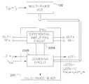
- FIG. 1is a circuit diagram of the VCO-mixer according to a background art.
- the VCO 10includes four differential delay cells 12 , 14 , 16 and 18 and has a structure similar to a ring oscillator.
- the four delay cells 12 - 18are serially connected and generate a clock signal LO+ and an inverted clock signal LO ⁇ , each having a frequency of f 0 .
- a control circuit for the VCO 10 that generates a frequency control signalincludes a phase frequency detector 4 , a charge pump 6 and a loop filter 8 that outputs the frequency control signal to each of the delay cells 12 - 18 .
- the phase frequency detector 4receives a reference clock signal f ref and a VCO clock signal f VCO from a reference clock divider circuit 2 and a VCO clock divider circuit 3 , respectively.
- the frequency f 0is based on the reference clock signal f ref and the divider circuits 2 and 3 .
- the mixer 20such as Gilbert—Multiplier, multiplies the input signals, such as radio frequency (RF) signals RF+ and RF ⁇ , with the clock signals LO+ and LO ⁇ .
- the mixer 20includes two load resistors R 1 and R 2 coupled to a source voltage V DD , eight NMOS transistors 21 - 28 , and a current source I S1 .
- the gates of the NMOS transistors 21 and 22are coupled to receive the clock signal LO+, and the gates of the NMOS transistors 23 and 24 are coupled to receive the inverted clock signal LO ⁇ .
- the gates of the NMOS transistors 25 and 26receive a common bias voltage V Bias .
- the gates of the NMOS transistors 27 and 28receive the RF signals RF+ and RF ⁇ , respectively. Therefore, the clock signals LO+ and LO ⁇ are multiplied with the RF signals RF+ and RF ⁇ only when the transistors 25 and 27 or the transistors 26 and 28 are turned on together.
- the output signals OUT+ and OUT ⁇ of the mixer 20has a frequency lower than its original frequency by the frequency f 0 of the clock signals LO+, LO ⁇ .
- the VCO-mixer structure 10 and 20can only support up to a frequency 1 GHz with reliable phase noise and frequency range.
- the performance of the VCO-mixer structure 10 and 20becomes worse in terms of phase noise and frequency range and is unacceptable as the frequency of the clock signals LO+ and LO ⁇ from the VCO increases.
- the VCO 10 and the mixer 20cannot be readily implemented when the frequency f 0 of the clock signals LO+ and LO ⁇ is over 1 GHz.
- An object of the inventionis to solve at least the above problems and/or disadvantages and to provide at least the advantages described hereinafter.
- a further object of the present inventionis to provide a VCO-mixer and method for using same on a single substrate.
- Another object of the present inventionis to increase the frequency range of a apparatus mixer and method.
- Still another object of the present inventionis to provide a mixer and method for using same having reduced noise.
- Another object of the present inventionis to increase a performance of the mixer structure.
- a further object of the present inventionis to provide a single/double balanced mixer and method having a symmetric switch structure.
- a further object of the present inventionis to fabricate a RF communications receiver on a single substrate.
- a further object of the present inventionis to provide a RF communications transceiver and method including a multi-phase mixer on a single substrate.
- a circuitthat includes a mixer that receives a plurality of first clock signals having different phases, each first clock signal having a first frequency which is less than a reference frequency, wherein the mixer mixes the plurality of first clock signals to generate a plurality of local oscillator signals therein having a higher second frequency, and wherein the mixer multiplies the plurality of local oscillator signals with input signals to provide output signals at output terminals.
- a method for modulating input signalsthat includes generating a plurality of first clock signals having different phases, each first clock signal having a first frequency that is less than a reference frequency of an input signal, combining the plurality of first clock signals to generate a plurality of local oscillator signals having a second frequency higher than the first frequency and mixing the plurality of local oscillator signals with the input signal to provide an output signal.
- a receiverthat includes an antenna that receives input signals being analog RF signals, a low noise amplifier coupled to the antenna, a clock generator that receives a reference signal having a reference frequency that generates a plurality of first clock signals having N different phases, N being an integer greater than two, each first clock signal having a first frequency substantially equal to double the reference frequency divided by N, a mixer coupled to the clock generator and the low noise amplifier that receives the plurality of first clock signals to generate at least one local oscillator signal therein having approximately the second frequency, wherein the mixer multiplies the at least one local oscillator signal with input signals to provide output signals at output terminals, a channel selection filter that removes an out-of-band signal from the demodulated baseband signal and an analog-to-digital converter that converts the demodulated baseband signal to a digital data stream.
- FIG. 1is a circuit diagram of a related art VCO-mixer structure
- FIG. 2Ais a block diagram showing a VCO-mixer structure according to a preferred embodiment of the present invention.
- FIG. 2Bis a circuit diagram showing a VCO-mixer structure of FIG. 2A;
- FIG. 3is a circuit diagram showing the VCO-mixer according to another preferred embodiment of the present invention.
- FIGS. 4A-4Hare operational timing diagrams showing a mixer of FIG. 3;
- FIG. 5is a circuit diagram showing yet another preferred embodiment of a mixer according to the present invention.
- FIG. 6is a circuit diagram showing an exemplary quadrature down converter according to the third preferred embodiment.
- FIG. 7is a circuit diagram showing still yet another preferred embodiment of a mixer according to the present invention.
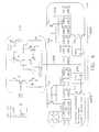
- FIG. 2Ais a block diagram that illustrates a VCO-mixer structure in accordance with a first preferred embodiment of the present invention.
- the structurecan be used for a RF communications system.
- the structureincludes a multi-phase voltage controlled oscillator VCO 100 and a multi-phase mixer 200 .
- the multi-phase mixer 200includes a differential amplifying circuit 200 A and a combining circuit 200 B.
- the plurality of N-phase intermediate clock signals LO( 0 ), LO( 1 ), . . . ,LO(N ⁇ 1) having a frequency of 2*f 0 /Nis inputted into the combining circuit 200 B of the multi-phase mixer 200 , and the input signals, for example, RF signals RF+ and RF ⁇ are inputted into the differential amplifying circuit 200 A.
- the differential amplifying circuit 200 Bdifferentially amplifies the radio frequency signals RF+ and RF ⁇ .
- the combining circuit 200 Bis responsive to a bias voltage V Bias and preferably combines the N-phase intermediate clock signals LO( 0 )-LO(N ⁇ 1) to generate the output clock signals LOT+ and LOT ⁇ having the original frequency f 0 .
- the mixer 200then accomplishes a multiplication of the output clock signals LOT+ and LOT ⁇ and the RF signals RF+ and RF ⁇ .
- FIG. 2Billustrates a circuit diagram of the VCO-mixer structure 100 , 200 in accordance with a first preferred embodiment.
- the multi-phase VCO 100includes N D number of delay cells 100 1 - 100 ND coupled in series. Based on such configuration, the multi-phase VCO generates a plurality of N-phase intermediate clock signals LO( 0 )-LO(N ⁇ 1) having a frequency of 2*f 0 /N.
- a control circuit for the VCO 100 that generates a frequency control signalincludes a phase frequency detector 54 , a charge pump 56 and a loop filter 58 that outputs the frequency control signal to each of the delay cells 100 1 - 100 ND .
- the phase frequency detector 54receives a reference clock signal f ref and a VCO clock signal f VCO from a reference clock divider circuit 52 and a VCO clock divider circuit 53 , respectively.
- the frequency f 0is based on the reference clock signal f ref and the divider circuits 52 and 53 .
- f VCOcan be 2f 0 /N by setting M′/K′ of the divider circuits 52 and 53 .
- the differential amplifying circuit 200 A of the multi-phase mixer 200includes two load resistors R 1 ′ and R 2 ′ coupled to two differential amplifiers 200 A 1 and 200 A 2 , respectively.
- the differential amplifier 200 A 1includes two NMOS transistors 210 and 212
- the differential amplifier 200 A 2includes two NMOS transistors 214 and 216 .
- the drains of the NMOS transistor 210 and 216are coupled to the load resistors R 1 ′ and R 2 ′, respectively, and the gates of the NMOS transistors 210 and 216 are coupled for receiving the RF signal RF+.
- the drains of the NMOS transistors 212 and 214are coupled to the load resistors R 2 ′ and R 1 ′, respectively, and the gates are coupled for receiving the RF signal RF ⁇ .
- the sources of NMOS transistors 210 and 212 and NMOS transistors 214 and 216are coupled to each other and to the combining circuit 200 B of the multi-phase mixer.
- the differential amplifiers 200 A 1 and 200 A 2differentially amplifies the RF signals RF+ and RF ⁇ , respectively, such that a more accurate output signals OUT ⁇ and OUT+ can be obtained. Further, the differential amplification removes noise that may have been added to the RF signals RF+ and RF ⁇ .
- the mixer 200is a type of multi-phase double-balanced mixer. In this preferred embodiment, two differential amplifiers 200 A 1 and 200 A 2 are included, however, the present invention may be also accomplished using only one of the differential amplifiers in alternative embodiments.
- the combining circuit 200 Bincludes bias NMOS transistors 232 and 234 , first combining unit 200 B 1 and second combining unit 200 B 2 coupled to the bias NMOS transistors 232 and 234 , respectively, and a current source I s1′ coupled to the first and second combining units 200 B 1 and 200 B 2 .
- the first combining unit 200 B 1includes a plurality of transistor units 220 0 , 220 2 . . . 220 N ⁇ 2
- the second combining unitincludes a second plurality of transistor units 220 1 , 220 3 . . . 220 N ⁇ 1 .
- each of the plurality of transistor unitsincludes a plurality of serially connected transistors, wherein the serially connected transistors are coupled in parallel with the serially connected transistors of the plurality of transistor units.
- each transistor unitincludes two (2) serially connected transistors.
- the bias NMOS transistors 232 and 234are included for prevention of error, however, such transistors may be omitted in alternative embodiments.
- the sequential ON-OFF operation of the 2*N number NMOS transistors of the combining circuit 200 Bis equivalent to a NAND logic circuit, which can be interchanged with other equivalent logic circuits and structure in alternative embodiments.
- the generic FIG. 2B structureallows integration of the multi-phase VCO 100 and multi-phase mixer 200 on a single chip, i.e., on a single semiconductor substrate using CMOS technology. Such structure and layout reduce noise including noise caused by parasitic capacitances. As described above, the differential amplification using the RF signals RF+ and RF ⁇ in the differential amplifying circuit 200 A reduces noise.
- the reduction of the reference frequency f 0 to N-phase intermediate clock signals LO(i) having a frequency of 2*f 0 /Nalso reduces noise.
- a plurality of transistorsare formed on the same substrate, such as a semiconductor substrate for CMOS technology, a plurality of P-N junctions are formed in the substrate.
- the parasitic capacitancesmostly exist at the P-N junctions. If the frequency of a signal applied to the gate of the transistor is very high, the higher frequency of f 0 causes much more noise compared to a reduced frequency of 2*f 0 /N.
- the operation of the differential amplifier circuit 200 A and the combining circuit 200 Bis dependent on the output clock signals LOT+ and LOT ⁇ having a frequency of f 0 , which are provided by the first combining unit 200 B 1 and second combining unit 200 B 2 , respectively, by combining the N-phase intermediate clock signals LO(i) having a frequency of 2*f 0 /N.
- the bias voltage V Biasis applied, the NMOS transistors 232 and 234 are turned ON and OFF based on the output clock signals LOT+ and LOT ⁇ .
- the NMOS transistors 210 , 212 , 214 and 216are turned ON by the RF signals RF+ and RF ⁇ applied to the gate electrodes, the amplification of the RF signals RF+ and RF ⁇ and the output clock signals LOT+ and LOT ⁇ for generating the output signals OUT+ and OUT ⁇ is performed when the bias NMOS transistors 232 and 234 are turned on by the clock signals LOT+ and LOT ⁇ .
- the multi-phase VCO 110includes three delay cells 110 1 - 110 3 to generate 6-phase intermediate clock signals LO( 0 )-LO( 5 ).
- An exemplary circuit including five transistors for the delay cells 110 1 - 110 3i.e., the delay cell 110 1
- the 6-phase intermediate clock signals LO( 0 )-LO( 5 )will have a frequency of 0.5 GHz.
- the 6-phase mixer 250includes a differential amplifying circuit 250 A and a combining circuit 250 B.
- the differential amplifying circuit 250 Aincludes a first differential amplifier 250 A 1 having NMOS transistors 260 and 262 and a second differential amplifier 250 A 2 having NMOS transistors 264 and 266 , which are coupled to load resistors R 3 and R 4 , respectively.
- the combining circuit 250 Bincludes a first combining unit 250 B 1 and 250 B 2 , which are commonly coupled to a current source I S2 .
- the first and second combining units 250 B 1 and 250 B 2are coupled to the first and second differential amplifiers 250 A 1 and 250 A 2 through bias NMOS transistors 282 and 284 , respectively, which are biased by a bias voltage V Bias .
- the first and second combining units 250 B 1 and 250 B 2includes six transistor units 270 0 - 270 5 with a total of twelve transistors.
- the 6-phase VCO 110generates 6-phase intermediate clock signals LO( 1 )-LO( 5 ) having the reduced frequency f 0 /3.
- the 6-phase mixer 250receives the 6-phase intermediate clock signals LO( 1 )-LO( 5 ) and the RF signals RF+ and RF ⁇ .
- the first and second combining units 250 B 1 and 250 B 2combine the 6-phase intermediate clock signals LO( 0 ), LO( 1 ), . . . LO( 4 ), LO( 5 ) having the frequency f 0 /3 to generate the output clock signals LOT+ and LOT ⁇ having the frequency f 0 .
- Each pair of NMOS transistors in the combining circuitare turned on in order, thereby producing the output signals LOT+ and LOT ⁇ , as shown in FIGS. 4G and 4H.
- FIG. 5illustrates a third preferred embodiment of a multi-phase single balanced mixer according to the present invention.
- the third preferred embodiment of a multi-phase mixer 500is a type of single balanced mixer.
- the multi-phase mixer 500preferably receives N-phase, 2*f 0 /N MHz LO clocks (LO ( 0 :N ⁇ 1)) and an RF signal and performs multiplication equivalent a single balanced mixer, which receives a single-phase f 0 MHz LO clock and the RF signal.
- LO2*f 0 /N MHz LO clocks
- the multi-phase single balanced mixer 500preferably includes four functional blocks being a load block 510 , a switch array block 520 , a noise reduction block 530 and an input block 540 .
- load block 510preferably includes two PMOS transistors 511 , 512 and two load resistors 513 , 514 .
- the two PMOS transistors 511 , 512have source electrodes coupled to a source voltage V DD and gate electrodes commonly coupled together.
- the load resistors 513 , 514are respectively coupled between the gate electrodes and drain electrodes of the PMOS transistors 511 , 512 .
- the PMOS transistors 511 , 512preferably are operating on a saturation region to provide high-impedance, and the resistors 513 , 514 serve as a load resistance.
- the parallel combination of the resistor 513 and the output impedance of PMOS transistor 511operates close to just the resistance of the resistor 513 because the output impedance of transistor 511 is large compared with the resistor 513 .
- the parallel combination of the resistor 514 and the output impedance of transistor 512is close to just the resistor 516 .
- the drain electrodes of the transistors 511 and 512are respectively coupled to first and second switch networks 520 A and 520 B of a switch array block 520 that perform multiplication of the multi-phase clock.
- a first switch network 520 Aincludes a plurality of transistor units 522 0 , 522 2 , . . . , 522 N ⁇ 2
- a second switch network 520 Bincludes a second plurality of transistor units 522 1 , 522 3 , . . . , 522 N ⁇ 1 .
- the N-phase single-balanced mixer 500receives N-phase clock signals LO[ 0 :N ⁇ 1] and the RF signal.
- the LO signalswould be LO[ 0 : 5 ].
- the switch array block 520provides a mechanism to obtain the resultant effect equivalent to applying a single phase signal whose frequency is F 0 by using the N-phase LO signals whose frequency is 2*f 0 /N.
- the N-phase single-balanced mixer 500according to the third preferred embodiment includes N switches controlled by N-phase LO signals. One of the N 2
- switches 522 j in the second switch network 520 Bis alternately turned on at every phase interval as shown in FIGS. 4A-4F.
- virtual waveforms LOT+ and LOT ⁇ as shown in FIGS. 4G-4Hare obtained by the multi-phase operation at output terminal IOUT ⁇ and IOUT+, respectively.
- each of the switches 522 0 - 522 N ⁇ 1includes at least first and second pluralities of serially coupled transistors.
- each of the switches 522 0 - 522 Nincludes transistor 524 A coupled in series with transistor 524 C and transistor 524 B connected in series with transistor 524 D.
- gate electrodes of the transistors 524 A and 524 Dare commonly coupled to receive a corresponding multi-phase clock signal LO (e.g., LO( 0 ))
- gate electrodes of the transistors 524 B and 524 Care commonly coupled to receive a corresponding multi-phase clock signal LO (e.g., LO( 1 )B).
- the transistors 524 A and 524 Bfurther have source electrodes coupled to the load block 510 at the output terminal IOUT ⁇
- the transistors 524 C and 524 Dhave source electrodes coupled to a node 526 .
- each of the switches 522 0 - 522 N ⁇ 1includes four NMOS transistors.
- each of the switches 522 0 - 522 N ⁇ 1includes symmetric NMOS transistors to provide an equivalent or symmetric electrical conditions to the two input ports 525 A, 525 B of each of the switches 522 0 - 522 N ⁇ 1 .
- a noise reduction block 530preferably includes a cascode NMOS transistor 531 whose gate electrode is coupled to a bias voltage V Bias .
- the noise reduction blockoperates to isolate the input block from the switch network 520 to prohibit noise coupling to an input RF signal 550 .
- the bias NMOS transistor 531is included to prevent error, however, such transistors enabled by the bias voltage V Bias can be omitted in alternative embodiments.
- An input block 540includes NMOS transistor 541 coupled to receive the RF input signal 550 preferably from a low noise amplifier at a gate electrode.
- the transistor 541is coupled between the transistor 531 and the ground voltage.
- the input voltage of the transistor 540is converted to a current level by the transconductance of the transistor 541 .
- the plurality of N-phase clock signals LO( 0 ), LO( 1 ), . . . ,LO(N ⁇ 1) having a frequency of 2*f 0 /Nis inputted into the switch array block 520 of the multi-phase mixer 500 , and the RF input signal 550 is inputted into the transistor 541 .
- the load block 510can amplify the RF input signal 500 when the switch array block 520 preferably combines the N-phase clock signals LO( 0 )-LO(N ⁇ 1) to generate the output clock signals LOT+ and LOT ⁇ having the original frequency f 0 responsive to the transistor 531 receiving the bias voltage V Bias at the output terminals IOUT ⁇ , IOUT+.
- the mixer 500then accomplishes a multiplication of the output clock signals LOT+ and LOT ⁇ and the RF input signal 550 .
- the multi-phase single-balanced mixer 500can perform the operation equivalent to applying the high-frequency f 0 signal by using the reduced-frequency multi-phase LO clock signals.
- a 12-phase quadrature down converter as shown in FIG. 6can be composed of two six-phase single-balanced mixers 600 A, 600 B according to the third preferred embodiment.
- six-phase LO signals(LO[ 0 , 2 , 4 , 6 , 8 , 10 ]) are used for an I-channel down conversion and the remaining six-phase LO signals (LO[ 1 , 3 , 5 , 7 , 9 , 11 ]) are used for Q-channel down conversion.
- LO[ 0 , 2 , 4 , 6 , 8 , 10 ]are used for an I-channel down conversion
- the remaining six-phase LO signals(LO[ 1 , 3 , 5 , 7 , 9 , 11 ]) are used for Q-channel down conversion.
- the third preferred embodiment of the mixer structureallows the use of a large amplitude LO[ 0 : 11 ] signals having reduced rise/fall times, and thus increases mixer conversion gains and decreases noise.
- resistor and capacitor pairs 670can be added to an input path of an RF signal 650 .
- a load block 610can be shared by the mixers 600 A, 600 B in alternative embodiments.
- two double-balanced mixerscan be used to construct a quadrature down converter as shown in FIG. 7.
- a double-balanced mixer 700receives a differential RF input RF+, RF ⁇ in contrast to the single-balanced mixers 500 , 600 that can receive a single-ended RF input.
- the multi-phase double-balanced mixer 700incorporates a single load block 710 commonly coupled to first and second switch arrays 720 .
- Each switch 722 iuses a structure similar to the second preferred embodiment.
- a current source 780 coupled between the differential RF input and the ground voltagecan be incorporated to improve performance characteristics.
- preferred embodiments of a mixer and methods of using samehave various advantages.
- the preferred embodimentsallow robust and low noise VCO and mixer to be fabricated on a single substrate, preferably on a semiconductor substrate using CMOS technology.
- the preferred embodimentsreduce interference caused by the input signal and the input clock signal because the frequency of the multi-phase intermediate clock signals deviate from the carrier signal frequency and the modulation frequency.
- a phase locked loop (PLL) frequency rangecan be increased because the PLL frequency range is based on the reduced frequency multi-phase clock signal frequency condition.
- PLLphase locked loop
Landscapes
- Engineering & Computer Science (AREA)
- Computer Networks & Wireless Communication (AREA)
- Signal Processing (AREA)
- Power Engineering (AREA)
- Superheterodyne Receivers (AREA)
Abstract
Description


Claims (20)
Priority Applications (2)
| Application Number | Priority Date | Filing Date | Title |
|---|---|---|---|
| US09/709,315US6313688B1 (en) | 1998-07-24 | 2000-11-13 | Mixer structure and method of using same |
| US09/985,897US6512408B2 (en) | 1998-07-24 | 2001-11-06 | Mixer structure and method for using same |
Applications Claiming Priority (4)
| Application Number | Priority Date | Filing Date | Title |
|---|---|---|---|
| US09/121,863US6194947B1 (en) | 1998-07-24 | 1998-07-24 | VCO-mixer structure |
| US09/121,601US6335952B1 (en) | 1998-07-24 | 1998-07-24 | Single chip CMOS transmitter/receiver |
| US16487499P | 1999-11-12 | 1999-11-12 | |
| US09/709,315US6313688B1 (en) | 1998-07-24 | 2000-11-13 | Mixer structure and method of using same |
Related Parent Applications (2)
| Application Number | Title | Priority Date | Filing Date |
|---|---|---|---|
| US09/121,863Continuation-In-PartUS6194947B1 (en) | 1998-07-24 | 1998-07-24 | VCO-mixer structure |
| US09/121,601Continuation-In-PartUS6335952B1 (en) | 1998-07-24 | 1998-07-24 | Single chip CMOS transmitter/receiver |
Related Child Applications (1)
| Application Number | Title | Priority Date | Filing Date |
|---|---|---|---|
| US09/985,897ContinuationUS6512408B2 (en) | 1998-07-24 | 2001-11-06 | Mixer structure and method for using same |
Publications (1)
| Publication Number | Publication Date |
|---|---|
| US6313688B1true US6313688B1 (en) | 2001-11-06 |
Family
ID=27494369
Family Applications (2)
| Application Number | Title | Priority Date | Filing Date |
|---|---|---|---|
| US09/709,315Expired - LifetimeUS6313688B1 (en) | 1998-07-24 | 2000-11-13 | Mixer structure and method of using same |
| US09/985,897Expired - LifetimeUS6512408B2 (en) | 1998-07-24 | 2001-11-06 | Mixer structure and method for using same |
Family Applications After (1)
| Application Number | Title | Priority Date | Filing Date |
|---|---|---|---|
| US09/985,897Expired - LifetimeUS6512408B2 (en) | 1998-07-24 | 2001-11-06 | Mixer structure and method for using same |
Country Status (1)
| Country | Link |
|---|---|
| US (2) | US6313688B1 (en) |
Cited By (21)
| Publication number | Priority date | Publication date | Assignee | Title |
|---|---|---|---|---|
| US6462626B1 (en)* | 1998-09-22 | 2002-10-08 | Texax Instruments Incorporated | Quadrature output oscillator device |
| US6639447B2 (en)* | 2002-03-08 | 2003-10-28 | Sirific Wireless Corporation | High linearity Gilbert I Q dual mixer |
| US6687494B1 (en)* | 2000-06-30 | 2004-02-03 | International Business Machines Corporation | Low power radio telephone image reject mixer |
| US20040092241A1 (en)* | 2002-10-31 | 2004-05-13 | Bon-Kee Kim | Local oscillator using I/Q mismatch compensating circuit through LO path receiver using thereof |
| US6748204B1 (en)* | 2000-10-17 | 2004-06-08 | Rf Micro Devices, Inc. | Mixer noise reduction technique |
| US20040108916A1 (en)* | 2001-04-27 | 2004-06-10 | Kwong Kam Choon | Switch in uhf bandpass |
| US20050110554A1 (en)* | 2003-11-21 | 2005-05-26 | Micron Technology, Inc. | Digital phase mixers with enhanced speed |
| US20050110539A1 (en)* | 2003-11-26 | 2005-05-26 | Micron Technology, Inc. | Digital delay-locked loop circuits with hierarchical delay adjustment |
| US20050127965A1 (en)* | 2003-12-12 | 2005-06-16 | Micron Technology, Inc. | Generating multi-phase clock signals using hierarchical delays |
| US20050127964A1 (en)* | 2003-12-11 | 2005-06-16 | Micron Technology, Inc. | Digital frequency-multiplying DLLs |
| US20060066362A1 (en)* | 2004-09-28 | 2006-03-30 | Sharp Kabushiki Kaisha | Voltage-current conversion circuit, amplifier, mixer circuit, and mobile appliance using the circuit |
| US20060232315A1 (en)* | 2005-04-15 | 2006-10-19 | Seong-Hoon Lee | Variable delay line with multiple hierarchy |
| US20070033560A1 (en)* | 2005-08-04 | 2007-02-08 | Freescale Semiconductor Inc. | Clock tree adjustable buffer |
| US20070040588A1 (en)* | 2005-08-17 | 2007-02-22 | Brandt Braswell | Amplifier circuit for double sampled architectures |
| US20070116105A1 (en)* | 2005-11-16 | 2007-05-24 | Tero John P | Multiple receiver rf integrated circuit architecture |
| US20090116602A1 (en)* | 2007-11-07 | 2009-05-07 | Micron Technology, Inc. | High speed, wide frequency-range, digital phase mixer and methods of operation |
| WO2009083713A1 (en)* | 2007-12-28 | 2009-07-09 | Wolfson Microelectronics Plc | Frequency synthesiser apparatus and method |
| US20090268849A1 (en)* | 2008-04-23 | 2009-10-29 | Fenghao Mu | Passive Miser and Four-Phase Clocking Method and Apparatus |
| US20090270062A1 (en)* | 2008-04-23 | 2009-10-29 | Fenghao Mu | Passive Miser and Four-Phase Clocking Method and Apparatus |
| US20120196554A1 (en)* | 2004-01-28 | 2012-08-02 | Mediatek Inc. | High Dynamic Range Time-Varying Integrated Receiver for Elimination of Off-Chip Filters |
| US9984732B2 (en)* | 2016-04-19 | 2018-05-29 | Samsung Electronics Co., Ltd. | Voltage monitor for generating delay codes |
Families Citing this family (27)
| Publication number | Priority date | Publication date | Assignee | Title |
|---|---|---|---|---|
| US8126779B2 (en)* | 1999-04-11 | 2012-02-28 | William Paul Wanker | Machine implemented methods of ranking merchants |
| US7302429B1 (en)* | 1999-04-11 | 2007-11-27 | William Paul Wanker | Customizable electronic commerce comparison system and method |
| US6658066B1 (en)* | 2000-02-17 | 2003-12-02 | Skyworks Solutions, Inc. | Method and apparatus for multiple phase splitting for dual band IQ subharmonic mixer |
| TW484257B (en)* | 2000-10-06 | 2002-04-21 | Macronix Int Co Ltd | Frequency mixer of communication system |
| KR20050007617A (en)* | 2003-07-11 | 2005-01-21 | 윤광호 | Frequency Converter having Multi-Phase Mixer |
| KR101051568B1 (en)* | 2003-12-10 | 2011-07-22 | 텔레폰악티에볼라겟엘엠에릭슨(펍) | Mixing device |
| EP1542356B1 (en)* | 2003-12-10 | 2008-04-02 | Telefonaktiebolaget LM Ericsson (publ) | Mixer arrangement |
| US7099646B1 (en) | 2004-01-27 | 2006-08-29 | Marvell International Ltd. | Signal mixer having a single-ended input and a differential output |
| US7340233B2 (en)* | 2004-03-29 | 2008-03-04 | Intel Corporation | Integrated circuit and methods for third sub harmonic up conversion and down conversion of signals |
| US7187917B2 (en)* | 2004-03-29 | 2007-03-06 | Texas Instruments Incorporated | Current interpolation in multi-phase local oscillator for use with harmonic rejection mixer |
| JP2005328109A (en)* | 2004-05-12 | 2005-11-24 | Thine Electronics Inc | Equiphase multi-phase clock signal generator circuit and serial digital data receiving circuit using the same |
| WO2007109744A2 (en)* | 2006-03-21 | 2007-09-27 | Multigig Inc. | Dual pll loop for phase noise filtering |
| US7769361B2 (en)* | 2006-07-19 | 2010-08-03 | Qualcomm Incorporated | Systems, methods, and apparatus for frequency conversion |
| ATE512498T1 (en)* | 2006-08-09 | 2011-06-15 | St Ericsson Sa | SIGNAL PROCESSOR WITH A FREQUENCY CONVERTER |
| US8385475B2 (en)* | 2007-05-08 | 2013-02-26 | Nxp, B.V. | Calibration-free local oscillator signal generation for a harmonic-rejection mixer |
| US20090138329A1 (en)* | 2007-11-26 | 2009-05-28 | William Paul Wanker | Application of query weights input to an electronic commerce information system to target advertising |
| US8072255B2 (en)* | 2008-01-07 | 2011-12-06 | Qualcomm Incorporated | Quadrature radio frequency mixer with low noise and low conversion loss |
| JP2009232451A (en)* | 2008-02-29 | 2009-10-08 | Seiko Epson Corp | Mixer circuit and communication device including the same |
| JP2009284466A (en)* | 2008-04-21 | 2009-12-03 | Seiko Epson Corp | Mixer circuit, communication device, and electronic apparatus |
| US8467760B2 (en)* | 2009-07-02 | 2013-06-18 | Broadcom Corporation | Frequency translated filters for wideband applications |
| US8285241B2 (en) | 2009-07-30 | 2012-10-09 | Broadcom Corporation | Receiver apparatus having filters implemented using frequency translation techniques |
| KR101077228B1 (en)* | 2009-09-17 | 2011-10-27 | (주)에프씨아이 | mixer circuit |
| US8237485B2 (en)* | 2010-07-08 | 2012-08-07 | Quintic Holdings | System and method for multiple-phase clock generation |
| US8766719B2 (en) | 2011-10-17 | 2014-07-01 | Mediatek Inc. | Digitally-controlled power amplifier with bandpass filtering/transient waveform control and related digitally-controlled power amplifier cell |
| US8618837B2 (en) | 2011-10-17 | 2013-12-31 | Mediatek Inc. | Multi-stage digitally-controlled power amplifier |
| US11171608B2 (en)* | 2019-01-11 | 2021-11-09 | Academia Sinica | Mixing circuit |
| TWI719891B (en)* | 2020-04-22 | 2021-02-21 | 瑞昱半導體股份有限公司 | Bias compensation device and method for operating a bias compensation device |
Citations (23)
| Publication number | Priority date | Publication date | Assignee | Title |
|---|---|---|---|---|
| US5175729A (en) | 1991-06-05 | 1992-12-29 | Motorola, Inc. | Radio with fast lock phase-locked loop |
| US5408201A (en) | 1993-05-24 | 1995-04-18 | Nec Corporation | Frequency synthesizer using three subfrequency synthesizers for generating two different frequencies |
| US5418815A (en) | 1992-06-12 | 1995-05-23 | Kabushiki Kaisha Toshiba | Receiver adaptively operable for multiple signal transmission systems |
| US5438591A (en) | 1991-07-31 | 1995-08-01 | Kabushiki Kaisha Toshiba | Quadrature amplitude modulation type digital radio communication device and method for preventing abnormal synchronization in demodulation system |
| US5448772A (en) | 1994-08-29 | 1995-09-05 | Motorola, Inc. | Stacked double balanced mixer circuit |
| US5507025A (en) | 1993-11-02 | 1996-04-09 | Winegard Company | Method and apparatus for satellite receiver with variable predetection bandwidth |
| US5555182A (en) | 1995-05-04 | 1996-09-10 | Cyberex, Inc. | Source quality monitoring system |
| US5584062A (en) | 1994-01-24 | 1996-12-10 | Motorola, Inc. | Method and apparatus for compensating phase locked receivers |
| US5614868A (en) | 1995-10-24 | 1997-03-25 | Vlsi Technology, Inc. | Phase locked loop having voltage controlled oscillator utilizing combinational logic |
| US5640146A (en)* | 1995-02-24 | 1997-06-17 | Ntp Incorporated | Radio tracking system and method of operation thereof |
| US5734970A (en) | 1995-02-08 | 1998-03-31 | Sony Corporation | Single oscillator transceiver with multiple frequency converters |
| US5761617A (en) | 1994-06-30 | 1998-06-02 | Nec Corporation | PLL synthesizer radio paging receiver capable of reducing an average power consumption |
| US5794119A (en) | 1995-11-21 | 1998-08-11 | Stanford Telecommunications, Inc. | Subscriber frequency control system and method in point-to-multipoint RF communication system |
| US5861773A (en) | 1995-07-06 | 1999-01-19 | Sgs-Thomson Microelectronics S.A. | Circuit for detecting the locked condition of PSK or QAM |
| US5872810A (en) | 1996-01-26 | 1999-02-16 | Imec Co. | Programmable modem apparatus for transmitting and receiving digital data, design method and use method for said modem |
| US5880613A (en) | 1996-10-11 | 1999-03-09 | Kabushiki Kaisha Toshiba | Logic storing circuit and logic circuit |
| US5894592A (en) | 1997-04-17 | 1999-04-13 | Motorala, Inc. | Wideband frequency synthesizer for direct conversion transceiver |
| US5950119A (en) | 1994-12-21 | 1999-09-07 | University Of Bristol | Image-reject mixers |
| US5963855A (en) | 1996-01-17 | 1999-10-05 | Nokia Mobile Phones Limited | Method for extending the RSSI range and radio transceiver operating in accordance with this method |
| US6029059A (en)* | 1997-06-30 | 2000-02-22 | Lucent Technologies, Inc. | Quadrature mixer method and apparatus |
| US6084905A (en) | 1995-04-27 | 2000-07-04 | Hitachi, Ltd. | Frequency hopped wireless communication system and communication equipment using a preamble field and information transfer field succeeding the preamble field |
| US6097768A (en) | 1996-11-21 | 2000-08-01 | Dps Group, Inc. | Phase detector for carrier recovery in a DQPSK receiver |
| US6194947B1 (en)* | 1998-07-24 | 2001-02-27 | Global Communication Technology Inc. | VCO-mixer structure |
Family Cites Families (7)
| Publication number | Priority date | Publication date | Assignee | Title |
|---|---|---|---|---|
| US4755774A (en) | 1985-07-15 | 1988-07-05 | Motorola Inc. | Two-port synthesizer modulation system employing an improved reference phase modulator |
| US5012142A (en) | 1989-07-28 | 1991-04-30 | At&T Bell Laboratories | Differential controlled delay elements and skew correcting detector for delay-locked loops and the like |
| US5180994A (en) | 1991-02-14 | 1993-01-19 | The Regents Of The University Of California | Differential-logic ring oscillator with quadrature outputs |
| US5179303A (en) | 1991-10-24 | 1993-01-12 | Northern Telecom Limited | Signal delay apparatus employing a phase locked loop |
| JP2705538B2 (en) | 1993-09-22 | 1998-01-28 | 日本電気株式会社 | Shared receiver for CDMA mode and FM mode |
| DE19729634A1 (en) | 1997-07-10 | 1999-01-14 | Lg Semicon Co Ltd | Frequency synthesiser |
| US6175279B1 (en) | 1997-12-09 | 2001-01-16 | Qualcomm Incorporated | Amplifier with adjustable bias current |
- 2000
- 2000-11-13USUS09/709,315patent/US6313688B1/ennot_activeExpired - Lifetime
- 2001
- 2001-11-06USUS09/985,897patent/US6512408B2/ennot_activeExpired - Lifetime
Patent Citations (23)
| Publication number | Priority date | Publication date | Assignee | Title |
|---|---|---|---|---|
| US5175729A (en) | 1991-06-05 | 1992-12-29 | Motorola, Inc. | Radio with fast lock phase-locked loop |
| US5438591A (en) | 1991-07-31 | 1995-08-01 | Kabushiki Kaisha Toshiba | Quadrature amplitude modulation type digital radio communication device and method for preventing abnormal synchronization in demodulation system |
| US5418815A (en) | 1992-06-12 | 1995-05-23 | Kabushiki Kaisha Toshiba | Receiver adaptively operable for multiple signal transmission systems |
| US5408201A (en) | 1993-05-24 | 1995-04-18 | Nec Corporation | Frequency synthesizer using three subfrequency synthesizers for generating two different frequencies |
| US5507025A (en) | 1993-11-02 | 1996-04-09 | Winegard Company | Method and apparatus for satellite receiver with variable predetection bandwidth |
| US5584062A (en) | 1994-01-24 | 1996-12-10 | Motorola, Inc. | Method and apparatus for compensating phase locked receivers |
| US5761617A (en) | 1994-06-30 | 1998-06-02 | Nec Corporation | PLL synthesizer radio paging receiver capable of reducing an average power consumption |
| US5448772A (en) | 1994-08-29 | 1995-09-05 | Motorola, Inc. | Stacked double balanced mixer circuit |
| US5950119A (en) | 1994-12-21 | 1999-09-07 | University Of Bristol | Image-reject mixers |
| US5734970A (en) | 1995-02-08 | 1998-03-31 | Sony Corporation | Single oscillator transceiver with multiple frequency converters |
| US5640146A (en)* | 1995-02-24 | 1997-06-17 | Ntp Incorporated | Radio tracking system and method of operation thereof |
| US6084905A (en) | 1995-04-27 | 2000-07-04 | Hitachi, Ltd. | Frequency hopped wireless communication system and communication equipment using a preamble field and information transfer field succeeding the preamble field |
| US5555182A (en) | 1995-05-04 | 1996-09-10 | Cyberex, Inc. | Source quality monitoring system |
| US5861773A (en) | 1995-07-06 | 1999-01-19 | Sgs-Thomson Microelectronics S.A. | Circuit for detecting the locked condition of PSK or QAM |
| US5614868A (en) | 1995-10-24 | 1997-03-25 | Vlsi Technology, Inc. | Phase locked loop having voltage controlled oscillator utilizing combinational logic |
| US5794119A (en) | 1995-11-21 | 1998-08-11 | Stanford Telecommunications, Inc. | Subscriber frequency control system and method in point-to-multipoint RF communication system |
| US5963855A (en) | 1996-01-17 | 1999-10-05 | Nokia Mobile Phones Limited | Method for extending the RSSI range and radio transceiver operating in accordance with this method |
| US5872810A (en) | 1996-01-26 | 1999-02-16 | Imec Co. | Programmable modem apparatus for transmitting and receiving digital data, design method and use method for said modem |
| US5880613A (en) | 1996-10-11 | 1999-03-09 | Kabushiki Kaisha Toshiba | Logic storing circuit and logic circuit |
| US6097768A (en) | 1996-11-21 | 2000-08-01 | Dps Group, Inc. | Phase detector for carrier recovery in a DQPSK receiver |
| US5894592A (en) | 1997-04-17 | 1999-04-13 | Motorala, Inc. | Wideband frequency synthesizer for direct conversion transceiver |
| US6029059A (en)* | 1997-06-30 | 2000-02-22 | Lucent Technologies, Inc. | Quadrature mixer method and apparatus |
| US6194947B1 (en)* | 1998-07-24 | 2001-02-27 | Global Communication Technology Inc. | VCO-mixer structure |
Cited By (49)
| Publication number | Priority date | Publication date | Assignee | Title |
|---|---|---|---|---|
| US6462626B1 (en)* | 1998-09-22 | 2002-10-08 | Texax Instruments Incorporated | Quadrature output oscillator device |
| US6687494B1 (en)* | 2000-06-30 | 2004-02-03 | International Business Machines Corporation | Low power radio telephone image reject mixer |
| US6748204B1 (en)* | 2000-10-17 | 2004-06-08 | Rf Micro Devices, Inc. | Mixer noise reduction technique |
| US20040108916A1 (en)* | 2001-04-27 | 2004-06-10 | Kwong Kam Choon | Switch in uhf bandpass |
| US7209726B2 (en)* | 2001-04-27 | 2007-04-24 | Pxp B.V. | Switch in UHF bandpass |
| US6639447B2 (en)* | 2002-03-08 | 2003-10-28 | Sirific Wireless Corporation | High linearity Gilbert I Q dual mixer |
| US20040092241A1 (en)* | 2002-10-31 | 2004-05-13 | Bon-Kee Kim | Local oscillator using I/Q mismatch compensating circuit through LO path receiver using thereof |
| US7116953B2 (en)* | 2002-10-31 | 2006-10-03 | Integrant Technologies Inc. | Local oscillator using I/Q mismatch compensating circuit through LO path receiver using thereof |
| US20060038603A1 (en)* | 2003-11-21 | 2006-02-23 | Micron Technology, Inc. | Digital phase mixers with enhanced speed |
| US20050110554A1 (en)* | 2003-11-21 | 2005-05-26 | Micron Technology, Inc. | Digital phase mixers with enhanced speed |
| US7161394B2 (en) | 2003-11-21 | 2007-01-09 | Micron Technology, Inc. | Digital phase mixers with enhanced speed |
| US6952127B2 (en) | 2003-11-21 | 2005-10-04 | Micron Technology, Inc. | Digital phase mixers with enhanced speed |
| US20050110539A1 (en)* | 2003-11-26 | 2005-05-26 | Micron Technology, Inc. | Digital delay-locked loop circuits with hierarchical delay adjustment |
| US7129761B2 (en) | 2003-11-26 | 2006-10-31 | Micron Technology, Inc. | Digital delay-locked loop circuits with hierarchical delay adjustment |
| US6982578B2 (en) | 2003-11-26 | 2006-01-03 | Micron Technology, Inc. | Digital delay-locked loop circuits with hierarchical delay adjustment |
| US20060071696A1 (en)* | 2003-11-26 | 2006-04-06 | Micron Technology, Inc. | Digital delay-locked loop circuits with hierarchical delay adjustment |
| US20050127964A1 (en)* | 2003-12-11 | 2005-06-16 | Micron Technology, Inc. | Digital frequency-multiplying DLLs |
| US6982579B2 (en) | 2003-12-11 | 2006-01-03 | Micron Technology, Inc. | Digital frequency-multiplying DLLs |
| US7372310B2 (en) | 2003-12-11 | 2008-05-13 | Micron Technology, Inc. | Digital frequency-multiplying DLLs |
| US20050285643A1 (en)* | 2003-12-11 | 2005-12-29 | Micron Technology, Inc. | Digital frequency-multiplying DLLs |
| US7173463B2 (en) | 2003-12-12 | 2007-02-06 | Micron Technology, Inc. | Generating multi-phase clock signals using hierarchical delays |
| US7009434B2 (en) | 2003-12-12 | 2006-03-07 | Micron Technology, Inc. | Generating multi-phase clock signals using hierarchical delays |
| US20060164140A1 (en)* | 2003-12-12 | 2006-07-27 | Micron Technology, Inc. | Generating multi-phase clock signals using hierarchical delays |
| US20050127965A1 (en)* | 2003-12-12 | 2005-06-16 | Micron Technology, Inc. | Generating multi-phase clock signals using hierarchical delays |
| US20070115036A1 (en)* | 2003-12-12 | 2007-05-24 | Micron Technology, Inc. | Generating multi-phase clock signals using hierarchical delays |
| US7339408B2 (en) | 2003-12-12 | 2008-03-04 | Micron Technology | Generating multi-phase clock signals using hierarchical delays |
| US8577323B2 (en)* | 2004-01-28 | 2013-11-05 | Mediatek, Inc. | High dynamic range time-varying integrated receiver for elimination of off-chip filters |
| US20120196554A1 (en)* | 2004-01-28 | 2012-08-02 | Mediatek Inc. | High Dynamic Range Time-Varying Integrated Receiver for Elimination of Off-Chip Filters |
| US20060066362A1 (en)* | 2004-09-28 | 2006-03-30 | Sharp Kabushiki Kaisha | Voltage-current conversion circuit, amplifier, mixer circuit, and mobile appliance using the circuit |
| US20060232315A1 (en)* | 2005-04-15 | 2006-10-19 | Seong-Hoon Lee | Variable delay line with multiple hierarchy |
| US7274236B2 (en) | 2005-04-15 | 2007-09-25 | Micron Technology, Inc. | Variable delay line with multiple hierarchy |
| US20070033560A1 (en)* | 2005-08-04 | 2007-02-08 | Freescale Semiconductor Inc. | Clock tree adjustable buffer |
| US7571406B2 (en)* | 2005-08-04 | 2009-08-04 | Freescale Semiconductor, Inc. | Clock tree adjustable buffer |
| US7917875B1 (en) | 2005-08-04 | 2011-03-29 | Freescale Semiconductor, Inc. | Clock tree adjustable buffer |
| US7449923B2 (en)* | 2005-08-17 | 2008-11-11 | Freescale Semiconductor, Inc. | Amplifier circuit for double sampled architectures |
| US20090033371A1 (en)* | 2005-08-17 | 2009-02-05 | Freescale Semiconductor, Inc. | Amplifier circuit for double sampled architectures |
| US20070040588A1 (en)* | 2005-08-17 | 2007-02-22 | Brandt Braswell | Amplifier circuit for double sampled architectures |
| US7595666B2 (en) | 2005-08-17 | 2009-09-29 | Freescale Semiconductor, Inc. | Amplifier circuit for double sampled architectures |
| US20070116105A1 (en)* | 2005-11-16 | 2007-05-24 | Tero John P | Multiple receiver rf integrated circuit architecture |
| US7907928B2 (en) | 2007-11-07 | 2011-03-15 | Micron Technology, Inc. | High speed, wide frequency-range, digital phase mixer and methods of operation |
| US8437726B2 (en) | 2007-11-07 | 2013-05-07 | Micron Technology, Inc. | High speed, wide frequency-range, digital phase mixer and methods of operation |
| US20090116602A1 (en)* | 2007-11-07 | 2009-05-07 | Micron Technology, Inc. | High speed, wide frequency-range, digital phase mixer and methods of operation |
| US8989692B2 (en) | 2007-11-07 | 2015-03-24 | Micron Technology, Inc. | High speed, wide frequency-range, digital phase mixer and methods of operation |
| WO2009083713A1 (en)* | 2007-12-28 | 2009-07-09 | Wolfson Microelectronics Plc | Frequency synthesiser apparatus and method |
| US20090270062A1 (en)* | 2008-04-23 | 2009-10-29 | Fenghao Mu | Passive Miser and Four-Phase Clocking Method and Apparatus |
| US20090268849A1 (en)* | 2008-04-23 | 2009-10-29 | Fenghao Mu | Passive Miser and Four-Phase Clocking Method and Apparatus |
| US8099070B2 (en) | 2008-04-23 | 2012-01-17 | Telefonaktiebolaget Lm Ericsson (Publ) | Passive mixer and four phase clocking method and apparatus |
| US8433277B2 (en) | 2008-04-23 | 2013-04-30 | Telefonaktiebolaget Lm Ericsson (Publ) | Passive mixer and four-phase clocking method and apparatus |
| US9984732B2 (en)* | 2016-04-19 | 2018-05-29 | Samsung Electronics Co., Ltd. | Voltage monitor for generating delay codes |
Also Published As
| Publication number | Publication date |
|---|---|
| US20020030529A1 (en) | 2002-03-14 |
| US6512408B2 (en) | 2003-01-28 |
Similar Documents
| Publication | Publication Date | Title |
|---|---|---|
| US6313688B1 (en) | Mixer structure and method of using same | |
| US6194947B1 (en) | VCO-mixer structure | |
| US6510185B2 (en) | Single chip CMOS transmitter/receiver | |
| US7519348B2 (en) | Harmonic suppression mixer and tuner | |
| US7248850B2 (en) | Passive subharmonic mixer design | |
| US8525573B2 (en) | Quadrature radio frequency mixer with low noise and low conversion loss | |
| US6144236A (en) | Structure and method for super FET mixer having logic-gate generated FET square-wave switching signal | |
| US8140044B2 (en) | Mixer circuit and method of operation | |
| US5768700A (en) | High conversion gain CMOS mixer | |
| US7792215B2 (en) | Direct-conversion receiver and sub-harmonic frequency mixer thereof | |
| KR100799473B1 (en) | Chopping Mixer and Direct Conversion Wireless Receiver | |
| CA2338564C (en) | Single chip cmos transmitter/receiver and vco-mixer structure | |
| JPH10135744A (en) | Method for mixing a plurality of frequency dependent input signal and mixer circuit | |
| US7039383B2 (en) | Quadrature mixer circuit including three-input local mixers | |
| EP2263308B1 (en) | A combined mixer and balun design | |
| US6937849B2 (en) | Mixing apparatus | |
| US8478219B2 (en) | Heterodyne receiver | |
| EP1425845B1 (en) | Harmonic mixer | |
| Liu et al. | A 60 GHz down-conversion passive mixer in 65 nm CMOS technology | |
| US7538596B2 (en) | Low distortion quadrature mixer and method therefor | |
| US6970687B1 (en) | Mixer | |
| WO2009059831A2 (en) | Mixing apparatus | |
| KR100872252B1 (en) | Harmonic rejection mixer | |
| US20040029544A1 (en) | Direct conversion circuit capable of eliminating distortion of base band signals |
Legal Events
| Date | Code | Title | Description |
|---|---|---|---|
| AS | Assignment | Owner name:GLOBAL COMMUNICATION TECHNOLOGY, INC., CALIFORNIA Free format text:ASSIGNMENT OF ASSIGNORS INTEREST;ASSIGNORS:LEE, KYEONGHO;JEONG, DEOG-KYOON;REEL/FRAME:011296/0001 Effective date:20001110 | |
| AS | Assignment | Owner name:GCT SEMICONDUCTOR, INC., CALIFORNIA Free format text:MERGER;ASSIGNOR:GLOBAL COMMUNICATION TECHNOLOGY, INC.;REEL/FRAME:011856/0127 Effective date:20010221 | |
| FPAY | Fee payment | Year of fee payment:4 | |
| SULP | Surcharge for late payment | ||
| REMI | Maintenance fee reminder mailed | ||
| REIN | Reinstatement after maintenance fee payment confirmed | ||
| FEPP | Fee payment procedure | Free format text:PETITION RELATED TO MAINTENANCE FEES FILED (ORIGINAL EVENT CODE: PMFP); ENTITY STATUS OF PATENT OWNER: SMALL ENTITY Free format text:PETITION RELATED TO MAINTENANCE FEES GRANTED (ORIGINAL EVENT CODE: PMFG); ENTITY STATUS OF PATENT OWNER: SMALL ENTITY | |
| FP | Lapsed due to failure to pay maintenance fee | Effective date:20091106 | |
| PRDP | Patent reinstated due to the acceptance of a late maintenance fee | Effective date:20100429 | |
| FPAY | Fee payment | Year of fee payment:8 | |
| STCF | Information on status: patent grant | Free format text:PATENTED CASE | |
| SULP | Surcharge for late payment | ||
| AS | Assignment | Owner name:COMERICA BANK, CALIFORNIA Free format text:INTELLECTUAL PROPERTY SECURITY AGREEMENT;ASSIGNOR:GCT SEMICONDUCTOR, INC.;REEL/FRAME:030112/0447 Effective date:20130313 | |
| FPAY | Fee payment | Year of fee payment:12 | |
| AS | Assignment | Owner name:GCT SEMICONDUCTOR, INC., CALIFORNIA Free format text:RELEASE BY SECURED PARTY;ASSIGNOR:COMERICA BANK;REEL/FRAME:037327/0085 Effective date:20151211 |