US6313498B1 - Flash memory cell with thin floating gate with rounded side wall, and fabrication process - Google Patents
Flash memory cell with thin floating gate with rounded side wall, and fabrication processDownload PDFInfo
- Publication number
- US6313498B1 US6313498B1US09/322,126US32212699AUS6313498B1US 6313498 B1US6313498 B1US 6313498B1US 32212699 AUS32212699 AUS 32212699AUS 6313498 B1US6313498 B1US 6313498B1
- Authority
- US
- United States
- Prior art keywords
- gate
- floating gate
- memory cell
- oxide
- control gate
- Prior art date
- Legal status (The legal status is an assumption and is not a legal conclusion. Google has not performed a legal analysis and makes no representation as to the accuracy of the status listed.)
- Expired - Lifetime
Links
- 238000000034methodMethods0.000titleabstractdescription21
- 230000008569processEffects0.000titleabstractdescription17
- 238000004519manufacturing processMethods0.000titledescription4
- 239000000758substrateSubstances0.000claimsabstractdescription12
- 229910021420polycrystalline siliconInorganic materials0.000claimsdescription6
- OAICVXFJPJFONN-UHFFFAOYSA-NPhosphorusChemical compound[P]OAICVXFJPJFONN-UHFFFAOYSA-N0.000claimsdescription5
- 229910052785arsenicInorganic materials0.000claimsdescription5
- RQNWIZPPADIBDY-UHFFFAOYSA-Narsenic atomChemical compound[As]RQNWIZPPADIBDY-UHFFFAOYSA-N0.000claimsdescription5
- 230000008878couplingEffects0.000claimsdescription5
- 238000010168coupling processMethods0.000claimsdescription5
- 238000005859coupling reactionMethods0.000claimsdescription5
- 229910052698phosphorusInorganic materials0.000claimsdescription5
- 239000011574phosphorusSubstances0.000claimsdescription5
- 229920005591polysiliconPolymers0.000claimsdescription5
- ZOXJGFHDIHLPTG-UHFFFAOYSA-NBoronChemical compound[B]ZOXJGFHDIHLPTG-UHFFFAOYSA-N0.000claimsdescription4
- 229910052796boronInorganic materials0.000claimsdescription4
- 229910021417amorphous siliconInorganic materials0.000claimsdescription3
- 150000004767nitridesChemical class0.000claimsdescription2
- 239000002210silicon-based materialSubstances0.000claims4
- 239000002019doping agentSubstances0.000claims2
- XUIMIQQOPSSXEZ-UHFFFAOYSA-NSiliconChemical compound[Si]XUIMIQQOPSSXEZ-UHFFFAOYSA-N0.000abstractdescription5
- 229910052710siliconInorganic materials0.000abstractdescription5
- 239000010703siliconSubstances0.000abstractdescription5
- 230000005684electric fieldEffects0.000description10
- 230000005689Fowler Nordheim tunnelingEffects0.000description5
- 238000003491arrayMethods0.000description5
- 230000003647oxidationEffects0.000description4
- 238000007254oxidation reactionMethods0.000description4
- 230000005641tunnelingEffects0.000description4
- 230000004888barrier functionEffects0.000description3
- 238000009792diffusion processMethods0.000description3
- 239000002784hot electronSubstances0.000description3
- 238000002347injectionMethods0.000description3
- 239000007924injectionSubstances0.000description3
- 238000013461designMethods0.000description2
- 238000010586diagramMethods0.000description2
- 238000005530etchingMethods0.000description2
- 239000000463materialSubstances0.000description2
- 229910052751metalInorganic materials0.000description2
- 239000002184metalSubstances0.000description2
- 125000006850spacer groupChemical group0.000description2
- 230000015572biosynthetic processEffects0.000description1
- 230000015556catabolic processEffects0.000description1
- 230000005465channelingEffects0.000description1
- 230000008021depositionEffects0.000description1
- 230000000694effectsEffects0.000description1
- 230000006870functionEffects0.000description1
- 238000011065in-situ storageMethods0.000description1
- 238000005468ion implantationMethods0.000description1
- 150000002500ionsChemical class0.000description1
- 238000002955isolationMethods0.000description1
- 230000000873masking effectEffects0.000description1
- 230000005012migrationEffects0.000description1
- 238000013508migrationMethods0.000description1
- 238000012986modificationMethods0.000description1
- 230000004048modificationEffects0.000description1
- 229910021421monocrystalline siliconInorganic materials0.000description1
- 238000012545processingMethods0.000description1
- 239000004065semiconductorSubstances0.000description1
Images


Classifications
- H—ELECTRICITY
- H10—SEMICONDUCTOR DEVICES; ELECTRIC SOLID-STATE DEVICES NOT OTHERWISE PROVIDED FOR
- H10D—INORGANIC ELECTRIC SEMICONDUCTOR DEVICES
- H10D30/00—Field-effect transistors [FET]
- H10D30/01—Manufacture or treatment
- H10D30/021—Manufacture or treatment of FETs having insulated gates [IGFET]
- H10D30/0411—Manufacture or treatment of FETs having insulated gates [IGFET] of FETs having floating gates
- H—ELECTRICITY
- H10—SEMICONDUCTOR DEVICES; ELECTRIC SOLID-STATE DEVICES NOT OTHERWISE PROVIDED FOR
- H10B—ELECTRONIC MEMORY DEVICES
- H10B69/00—Erasable-and-programmable ROM [EPROM] devices not provided for in groups H10B41/00 - H10B63/00, e.g. ultraviolet erasable-and-programmable ROM [UVEPROM] devices
- H—ELECTRICITY
- H10—SEMICONDUCTOR DEVICES; ELECTRIC SOLID-STATE DEVICES NOT OTHERWISE PROVIDED FOR
- H10D—INORGANIC ELECTRIC SEMICONDUCTOR DEVICES
- H10D30/00—Field-effect transistors [FET]
- H10D30/60—Insulated-gate field-effect transistors [IGFET]
- H10D30/68—Floating-gate IGFETs
- H10D30/681—Floating-gate IGFETs having only two programming levels
- H10D30/684—Floating-gate IGFETs having only two programming levels programmed by hot carrier injection
- H10D30/685—Floating-gate IGFETs having only two programming levels programmed by hot carrier injection from the channel
- H—ELECTRICITY
- H10—SEMICONDUCTOR DEVICES; ELECTRIC SOLID-STATE DEVICES NOT OTHERWISE PROVIDED FOR
- H10D—INORGANIC ELECTRIC SEMICONDUCTOR DEVICES
- H10D30/00—Field-effect transistors [FET]
- H10D30/60—Insulated-gate field-effect transistors [IGFET]
- H10D30/68—Floating-gate IGFETs
- H10D30/6891—Floating-gate IGFETs characterised by the shapes, relative sizes or dispositions of the floating gate electrode
- H—ELECTRICITY
- H10—SEMICONDUCTOR DEVICES; ELECTRIC SOLID-STATE DEVICES NOT OTHERWISE PROVIDED FOR
- H10D—INORGANIC ELECTRIC SEMICONDUCTOR DEVICES
- H10D64/00—Electrodes of devices having potential barriers
- H10D64/01—Manufacture or treatment
- H10D64/031—Manufacture or treatment of data-storage electrodes
- H10D64/035—Manufacture or treatment of data-storage electrodes comprising conductor-insulator-conductor-insulator-semiconductor structures
Definitions
- This inventionpertains generally to semiconductor devices and, more particularly, to a nonvolatile memory device and fabrication process.
- EPROMElectrically programmable read only memory
- UVUltra-Violet
- Electrically erasable programmable read only memoryovercomes this problem and permits data to be erased electrically in a much shorter period of time, typically less than 2 seconds. However, it still has a disadvantage in that the data must be erased on a byte-by-byte basis.
- Flash EEPROMis similar to EEPROM in that data is erased electrically and relatively quickly. However, with flash EEPROM, the data is erased in blocks which typically range in size from 128 to 64K bytes per block, rather than on a byte-by-byte basis.
- stack-gateIn general, there are two basic types of nonvolatile memory cell structures: stack-gate and split-gate.
- the stack-gate memory cellusually has a floating gate and a control gate, with the control gate being positioned directly above the floating gate.
- the control gateIn a split-gate cell the control gate is still positioned above the floating gate, but it is offset laterally from it.
- the fabrication process for a stack-gate cellis generally simpler than that for a split-gate cell.
- a stack-gate cellhas an over-erase problem which a split-gate cell does not have. This problem is commonly addressed by maintaining the threshold voltage of the cell in a range of about 0.5-2.0 volts after an erase cycle, which adds complexity to the circuit design.
- split-gate memory cellAlthough a split-gate memory cell has no over erase problem, it generally includes an additional gate known as a select gate. Such cells are typically fabricated in double-poly or triple-poly processes which involve relatively complex processing steps. In addition, split-gate cells are generally larger than stack-gate cells. Nevertheless, because of the relatively simple circuit design which is possible when there is no over-erase problem, split-gate cells are used widely, particularly in embedded nonvolatile memory applications.
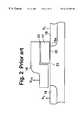
- FIG. 1illustrates split-gate memory cell having a control gate 16 which only partially overlies the floating gate 17 .
- the source 18is biased at a relatively high voltage of about 12 volts
- the control gateis biased at about 3 volts
- the drain 19is grounded.
- most of source-to-drain voltageis applied across the mid-channel region 21 between the control gate and the floating gate, creating a strong electric field in that region.
- the floating gateis coupled to the source node and is therefore at a higher voltage level than the mid-channel region, which produces a second electric field which extends vertically.
- That fieldaccelerates some of the hot electrons in the mid-channel region so that they exceed the energy barrier of the oxide layer 22 (about 3.1 eV) and are injected into floating gate. This technique is described in greater detail in U.S. Pat. Nos. 4,794,565, 5,029,130 and 5,455,792.
- the control gateIn the erase mode, the control gate is biased at a high voltage of about 15 volts, the source and drain nodes are biased at 0 volts, and the drain node is open. A high voltage is now formed across the inter-poly dielectric 23 between the floating gate and the control gate.
- the edge 17 a of the floating gatefunctions as a cathode electrode where Fowler-Nordheim tunneling takes place, and electrons flow from the floating gate to control gate, leaving the floating gate charged with positive ions.
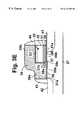
- FIG. 2illustrates a split-gate memory cell in which the control gate 16 completely overlies the floating gate 17 .
- the floating gateis coupled more closely to the control gate than to the source region, and the control gate is used for coupling voltages to the floating gate.
- hot carrier injectionis once again utilized for injecting electrons into the floating gate, with the control gate being biased at about 12 volts, drain 19 biased at 0 volts, and source 18 biased at about 7 volts.
- the control gatebeing biased at about 12 volts, drain 19 biased at 0 volts, and source 18 biased at about 7 volts.
- Some of the hot electronscan exceed the oxide barrier height and are injected into floating gate.
- Fowler-Nordheim tunnelingis utilized to force electrons to tunnel from the floating gate to the overlapped portion of the source region 18 a under the floating gate.
- a high electric fieldgreater than 10 mV/cm
- a high electric fieldis established across the thin oxide layer 22 by applying about 15 volts to the source node, 0 volts to the control gate, letting the drain node float.
- most of the voltage difference between the source and the control gateis applied across the thin oxide, triggering Fowler-Nordheim tunneling and forcing electrons to tunnel from the floating gate to the overlapped portion of the source region.
- This techniqueis also utilized in stack-gate cells, and is described in greater detail in U.S. Pat. Nos. 5,402,371, 5,284,784 and 5,445,792.
- U.S. Pat. No. 5,029,130shows a split-gate memory cell in which a sharp, upwardly curved edge is formed on the floating gate to create a well-defined charge injection edge in order to provide a high probability of electron tunneling.
- a third polycrystalline silicon layeras an erase layer which crosses over, or overlies, the floating gate and the control gate, an erase path can be formed between the side wall of floating gate and the erase layer. This technique is disclosed in U.S. Pat. Nos. 5,847,996 and 5,643,812.
- Fowler-Nordheim tunnelinghas also been utilized with both split-gate cells and stack-gate cells to form a negative charge on the floating gate in the programming mode, and U.S. Pat. No. 5,402,371 shows one example of a device in which electrons are forced to tunnel into the floating gate from the channel region beneath it.
- Another object of the inventionis to provide a memory cell and process of the above character which overcome the limitations and disadvantages of the prior art.
- a nonvolatile memory cell and processin which a thin floating gate is formed with a rounded lateral edge and a thickness on the order of 100-1000 ⁇ over a gate oxide in an active area on a silicon substrate.
- a tunnel oxideis formed adjacent to the rounded edge of the floating gate, and a control gate is formed with a lower portion next to the tunnel oxide and an upper portion overlying the floating gate.
- the upper portion of the control gatecompletely overlies the floating gate, and in others it only partially overlies it.
- FIGS. 1 and 2are cross-sectional views of split-gate memory cells of the prior art.
- FIGS. 3A-3Eare schematic cross sectional views illustrating the steps in one embodiment of a process for fabricating a flash memory cell in accordance with the invention.
- FIGS. 4A-4Dare schematic cross sectional views illustrating the steps in another embodiment of a process for fabricating a flash memory cell in accordance with the invention.
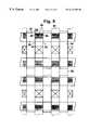
- FIG. 5is a top plan view of a NOR-type memory cell array fabricated in accordance with the process of either FIGS. 3A-3E or the process of FIGS. 4A-4D with self-aligned floating gates.
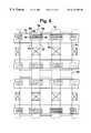
- FIG. 6is a top plan view of a NOR-type memory cell array fabricated in accordance with the process of either FIGS. 3A-3E or the process of FIGS. 4A-4D without self-aligned floating gates.
- FIG. 7is a circuit diagram of the NOR-type memory cell arrays illustrated in FIGS. 5 and 6 .
- an oxide layer 26 having a thickness on the order of 70-250 ⁇is thermally grown on a monocrystalline silicon substrate 27 for use as a gate oxide of a floating gate transistor.
- the substratecan be either a P-well or a P-substrate material.
- a layer 28 of polysilicon or amorphous silicon (the poly- 1 layer)is deposited on the oxide layer for use as a floating gate.
- the poly- 1 layerhas a thickness on the order of 100-1000 ⁇ , which is substantially thinner than the floating gates in prior art devices which are typically about 2000 ⁇ thick.
- the poly- 1 layeris preferably doped with phosphorus, arsenic or boron to a level on the order of 10 17 to 10 20 per cm 3 . The doping can be done in-situ during deposition of the silicon or by ion implantation.
- a dielectric film 29is then formed on the poly- 1 layer.
- this filmconsists of a bottom oxide layer 31 having a thickness on the order of 50-300 ⁇ , a central nitride layer 32 having a thickness on the order of 500-2000 ⁇ , and a top oxide layer 33 having a thickness on the order of 50-500 ⁇ .
- a photolithographic mask(not shown) is formed over the dielectric film to define the floating gate pattern, and the unmasked portions of the dielectric film and the poly- 1 layer are then etched away anisotropically, as illustrated in FIG. 3B to form a vertical edge 28 a along one side of the floating gate.
- a thermal oxidation stepis performed to form a gate oxide 36 on the silicon substrate and tunnel oxide 37 on the side wall or edge 28 a of the floating gate, as illustrated in FIG. 3 C.
- This portion of the gate oxidehas a thickness on the order of 100-400 ⁇ , and the tunnel oxide has a preferred thickness on the order of 50-300 ⁇ .
- a relatively thin CVD oxide 37 a(about 50-200 ⁇ ) can be deposited on the thermal oxide to improve the quality of the oxide films and reduce disturbances between the control gate and the floating gate.
- the lateral edge or side wall 28 a of the floating gatebecomes rounded because the oxidation rate for the poly- 1 layer is faster near the interfaces with oxide layers 26 , 31 .
- This rounded curvatureprovides an electric field enhancement which makes it much easier for electrons to tunnel out of the floating gate through this area.
- iteliminates the localized trapping effect which occurs in a tunnel oxide near square corners of poly- 1 . This enhances performance of the memory cell during both the program cycle and the erase cycle.
- the relatively thin poly- 1 layerprovides a correspondingly small tunneling window at the rounded edge of the floating gate. With a smaller tunneling window, the coupling ratio from the source region becomes larger, and that makes operation more efficient during erase cycles.
- a second polysilicon layer 39(the poly- 2 layer) is deposited over dielectric film 29 and gate oxide 36 , as illustrated in FIG. 3 D.
- This layerhas a thickness on the order of 1500-3000 ⁇ , and is doped with phosphorus, arsenic or boron to a level on the order of 10 20 to 10 21 per cm 3 .
- polycidecan be used in this layer to reduce the sheet resistance of the control gate.
- a second photolithographic mask(not shown) is formed on the poly- 2 layer to define the control gate and the previously undefined side of the floating gate.
- the unmasked portions of the poly- 2 layer, the dielectric film, and the poly- 1 layerare then etched away anisotropically, as shown in FIG. 3 E.
- the control gatehas a lower portion 39 a which is positioned to one side of the floating gate and an upper portion 39 b which overlies the floating gate.
- the lower portion of the control gateis separated from the rounded edge 28 a of the floating gate by tunnel oxide 37 , 37 a and the upper portion is separated from the floating gate by dielectric film 29 .
- the control gatecompletely overlies the floating gate, and the lateral edges of the two gates are self-aligned.
- a source region 41 and a drain region 42are formed in the active area of the substrate, and oxide spacers 43 , 44 are formed at the sides of the control gate. Both the source region and the drain region are heavily doped with an N-type material such as phosphorus or arsenic, and the source region is made with a deeper junction than the drain region. The deeper junction results in wider lateral diffusion of the source region and a larger area of overlap beneath the floating gate. It also provides a larger junction breakdown voltage which permits the source node to be biased to higher voltages during programming operations.
- FIGS. 4A-4Dis similar to the embodiment of FIGS. 3A-3E except that the control gate only partially overlies the floating gate, and the floating gate has two rounded side edges which serve as cathodes for electron tunneling.
- Like reference numeralsdesignate corresponding elements in the two embodiments.
- both side edges 28 a of the floating gateare delineated during the initial masking and etching steps. Both of these edges are rounded during the oxidation step, and tunnel oxide 37 , 37 a is formed on each side of the floating gate, as illustrated in FIG. 4 B.
- the poly- 2 layer 39is formed over the tunnel oxide on both sides of the floating gate, and with both side edges of the floating gate already formed, only the poly- 2 layer is etched during the second etching step.
- control gate 39overlies or covers only about one-half of the floating gate, and oxide spacer 44 covers the edge of the dielectric film, but not the control gate.
- FIGS. 5 and 6illustrate memory cell arrays which are made up of devices fabricated by the process of FIGS. 3A-3E, with the edges 46 of the floating gates aligned with the edges 47 of the control gates. Similar arrays can also be constructed with devices fabricated by the process of FIGS. 4A-4D, in which case the edges 46 of the floating gates will be offset from the edges 47 of the control gates, rather than being aligned with them.
- the memory cell array shown in FIG. 5has self-aligned floating gates, with the edges 48 , 49 of the floating gates being aligned with the edges 51 , 52 of the active areas.
- Preferred techniques for aligning the edges of the floating gates with the edges of the active areasare disclosed in Ser. No. 09/255,360, filed Feb. 23, 1999, incorporated herein by reference.
- the memory cell array illustrated in FIG. 6differs from the array of FIG. 5 in that it does not have self-aligned floating gates.
- the floating gates in this embodimenthave end caps 58 which extend over isolation oxide regions 54 . The end caps prevent short channeling or punchthrough which can occur because of pattern shifting or corner rounding during formation of the floating gate.
- bit lines 53which are typically made of metal and isolated from each other by oxide regions 54 .
- the sources of the memory cells in each roware connected together by a source line 56 which typically consists of an N+ diffusion layer in the silicon substrate.
- FIG. 7A circuit diagram for the memory cell arrays of FIGS. 5 and 6 is shown in FIG. 7 .
- all of the memory cells in a given columnhave their drains 42 connected to a metal bit line 53 that crosses over the active areas, and all of the cells in a given row have their sources 41 connected to a source line 56 which is typically an N+ diffusion layer in the substrate.
- All of the control gates 39 in a given roware connected together by the poly- 2 layer 39 from which the control gates are formed.
- a positive voltage on the order of 12 to 15 voltsis applied to the control gates, the drain nodes float, and the source nodes are biased to 0 volts.
- the coupling ratio between the source node and the floating gateis on the order of 70 to 85 percent, which means that about 70 to 85 percent of the source voltage is applied to the floating gate.
- Most of the voltage difference between the control gate and the sourceis therefore concentrated across the tunnel oxide between the curved edge(s) of the floating gate and the control gate, triggering Fowler-Nordheim tunneling and migration of electrons from the floating gate to the control gate.
- the floating gateis positively charged, and the threshold voltage of the memory cell drops to the range of ⁇ 5 to ⁇ 1 volts. This permits an inversion layer to form in the channel beneath the floating gate when the control gate is biased at 1.0 to 3.0 volts during a read operation. Thus, the cell is in a conducting, or logic “1”, state following the erase operation.
- the control gateis biased at 1.5 to 3.0 volts
- the drainis biased at about 0 volts
- the sourceis biased at 10 to 13 volts.
- Thisturns on the channel regions 59 a , 59 b beneath the control gate and the floating gate, which causes most of the source-to-drain voltage to be applied across the mid-channel region 59 c between the control gate and the floating gate.
- Thisproduces a strong electric field across the mid-channel region. Since the high voltage applied to the source is coupled to the floating gate, a strong electric field is also established across the oxide layer 26 between the floating gate and the mid-channel region.
- Electrons flowing from the drain toward the source during programmingare accelerated by the electric field in the mid-channel region, and some of them become heated.
- the hot electronsare also accelerated by the vertical electric field between the mid-channel region, and some of them exceed the barrier height (about 3.1 eV) of the oxide layer and are injected into the floating gate.
- This hot carrier injectioncauses the floating gate to become negatively charged, and the threshold voltage of the cell rises to a level of about 3.0 to 6.0 volts.
- the channel beneath the floating gateis now turned off, and the cell is in a non-conducting, or logic “0”, state.
- the sourceis biased to 0 volts
- the drainis biased to 1.5 to 3.0 volts
- the control gateis biased to 1.0 to 3.0 volts.
- the readshows a conduction state because both the floating gate and the control gate channels are turned on, and the sense amplifier reads a logic “1”.
- the readshows a non.conducting state because the floating gate channel is turned off, and the sense amplifier reads a logic “0”.
- the bias voltages applied to the terminal nodesare set forth in Table 2.
- the coupling ratiobecomes larger, e.g. 80 to 90 percent, and more voltage can be coupled from the source and P-well nodes to the floating gate.
Landscapes
- Non-Volatile Memory (AREA)
- Semiconductor Memories (AREA)
Abstract
Description
| TABLE 1 | ||||||||
| Mode | Control Gate | Drain | Source | |||||
| Erase | 12-15 | volts | Floating | 0 | volts |
| Program | 1.5-3 | volts | 0 | volts | 10-13 | volts | ||
| Read | 1-3 | volts | 1.5-3 | volts | 0 | volts | ||
| TABLE 2 | ||||
| Mode | Control Gate | Drain | Source | P-Well |
| Erase | 6 to 9 | volts | Floating | −9 to −6 | volts | −9 to |
| −6 volts |
| Program | 1.5 to 3 | volts | 0 | volts | 10 to 13 | volts | 0 volts |
| or | |||||||
| Floating | |||||||
| 1 to 3 | volts | 1.5 to 3 | volts | 0 | volts | 0 volts | |
| or | |||||||
| Floating | |||||||
Claims (13)
Priority Applications (1)
| Application Number | Priority Date | Filing Date | Title |
|---|---|---|---|
| US09/322,126US6313498B1 (en) | 1999-05-27 | 1999-05-27 | Flash memory cell with thin floating gate with rounded side wall, and fabrication process |
Applications Claiming Priority (1)
| Application Number | Priority Date | Filing Date | Title |
|---|---|---|---|
| US09/322,126US6313498B1 (en) | 1999-05-27 | 1999-05-27 | Flash memory cell with thin floating gate with rounded side wall, and fabrication process |
Publications (1)
| Publication Number | Publication Date |
|---|---|
| US6313498B1true US6313498B1 (en) | 2001-11-06 |
Family
ID=23253549
Family Applications (1)
| Application Number | Title | Priority Date | Filing Date |
|---|---|---|---|
| US09/322,126Expired - LifetimeUS6313498B1 (en) | 1999-05-27 | 1999-05-27 | Flash memory cell with thin floating gate with rounded side wall, and fabrication process |
Country Status (1)
| Country | Link |
|---|---|
| US (1) | US6313498B1 (en) |
Cited By (16)
| Publication number | Priority date | Publication date | Assignee | Title |
|---|---|---|---|---|
| US6642571B2 (en)* | 2001-10-18 | 2003-11-04 | Sanyo Electric Co., Ltd. | Nonvolatile semiconductor memory |
| US20050093055A1 (en)* | 2003-11-05 | 2005-05-05 | Leo Wang | Flash memory and method thereof |
| US20050164453A1 (en)* | 2004-01-22 | 2005-07-28 | Hiroyuki Fukunaga | Method of manufacturing nonvolatile semiconductor storage device |
| CN1302553C (en)* | 2003-04-16 | 2007-02-28 | 力晶半导体股份有限公司 | Split gate flash memory cell and manufacturing method thereof |
| US20070262368A1 (en)* | 2006-04-20 | 2007-11-15 | Ko-Hsing Chang | Non-volatile memory and manufacturing method thereof |
| US20080061348A1 (en)* | 2006-09-08 | 2008-03-13 | Samsung Electronics Co., Ltd. | Nonvolatile memory structure and method of forming the same |
| US20080182889A1 (en)* | 2002-06-11 | 2008-07-31 | Eric David Moher | Prodrugs of excitatory amino acids |
| US20080290394A1 (en)* | 2007-05-23 | 2008-11-27 | Xiangfeng Duan | Gate electrode for a nonvolatile memory cell |
| CN101170064B (en)* | 2006-10-23 | 2010-05-12 | 上海华虹Nec电子有限公司 | Method for flash technology high-voltage bar oxygen and tunnel-penetration oxidation layer |
| US20100163965A1 (en)* | 2008-12-31 | 2010-07-01 | Young Jun Kwon | Flash memory device and manufacturing method of the same |
| US20100207196A1 (en)* | 2009-02-16 | 2010-08-19 | Shin Min Jung | Semiconductor device having internal gate structure and method for manufacturing the same |
| US20110165749A1 (en)* | 2010-01-07 | 2011-07-07 | Winstead Brian A | Method of making a semiconductor structure useful in making a split gate non-volatile memory cell |
| US8502296B1 (en) | 2008-07-07 | 2013-08-06 | National Semiconductor Corporation | Non-volatile memory cell with asymmetrical split gate and related system and method |
| US8643123B2 (en) | 2011-04-13 | 2014-02-04 | Freescale Semiconductor, Inc. | Method of making a semiconductor structure useful in making a split gate non-volatile memory cell |
| US8648406B2 (en)* | 2011-12-29 | 2014-02-11 | Dongbu Hitek Co., Ltd. | Single poly EEPROM having a tunnel oxide layer |
| US10644011B1 (en) | 2018-11-09 | 2020-05-05 | Iotmemory Technology Inc. | Non-volatile memory |
Citations (14)
| Publication number | Priority date | Publication date | Assignee | Title |
|---|---|---|---|---|
| US4698787A (en) | 1984-11-21 | 1987-10-06 | Exel Microelectronics, Inc. | Single transistor electrically programmable memory device and method |
| US4794565A (en) | 1986-09-15 | 1988-12-27 | The Regents Of The University Of California | Electrically programmable memory device employing source side injection |
| US5029130A (en) | 1990-01-22 | 1991-07-02 | Silicon Storage Technology, Inc. | Single transistor non-valatile electrically alterable semiconductor memory device |
| US5095344A (en)* | 1988-06-08 | 1992-03-10 | Eliyahou Harari | Highly compact eprom and flash eeprom devices |
| US5284784A (en) | 1991-10-02 | 1994-02-08 | National Semiconductor Corporation | Buried bit-line source-side injection flash memory cell |
| US5286994A (en)* | 1991-08-22 | 1994-02-15 | Rohm Co., Ltd. | Semiconductor memory trap film assembly having plural laminated gate insulating films |
| US5402371A (en) | 1992-10-09 | 1995-03-28 | Oki Electric Industry Co., Ltd. | Method of writing data into and erasing the same from semiconductor nonvolatile memory |
| US5455792A (en) | 1994-09-09 | 1995-10-03 | Yi; Yong-Wan | Flash EEPROM devices employing mid channel injection |
| US5500384A (en) | 1993-09-08 | 1996-03-19 | Siemens Aktiengesellschaft | Method for manufacturing a bit line via hole in a memory cell |
| US5643812A (en) | 1993-10-28 | 1997-07-01 | Goldstar Electron Co., Ltd. | Method of making EEPROM flash memory cell with erase gate |
| US5767005A (en) | 1993-07-27 | 1998-06-16 | Micron Technology, Inc. | Method for fabricating a flash EEPROM |
| US5770501A (en) | 1995-12-22 | 1998-06-23 | United Microelectronics Corporation | Process of fabricating NAND-structure flash EEPROM using liquid phase deposition |
| US5792670A (en) | 1993-02-19 | 1998-08-11 | Sgs-Thomson Microelectronics S.R.L. | Method of manufacturing double polysilicon EEPROM cell and access transistor |
| US5847996A (en) | 1992-01-14 | 1998-12-08 | Sandisk Corporation | Eeprom with split gate source side injection |
- 1999
- 1999-05-27USUS09/322,126patent/US6313498B1/ennot_activeExpired - Lifetime
Patent Citations (14)
| Publication number | Priority date | Publication date | Assignee | Title |
|---|---|---|---|---|
| US4698787A (en) | 1984-11-21 | 1987-10-06 | Exel Microelectronics, Inc. | Single transistor electrically programmable memory device and method |
| US4794565A (en) | 1986-09-15 | 1988-12-27 | The Regents Of The University Of California | Electrically programmable memory device employing source side injection |
| US5095344A (en)* | 1988-06-08 | 1992-03-10 | Eliyahou Harari | Highly compact eprom and flash eeprom devices |
| US5029130A (en) | 1990-01-22 | 1991-07-02 | Silicon Storage Technology, Inc. | Single transistor non-valatile electrically alterable semiconductor memory device |
| US5286994A (en)* | 1991-08-22 | 1994-02-15 | Rohm Co., Ltd. | Semiconductor memory trap film assembly having plural laminated gate insulating films |
| US5284784A (en) | 1991-10-02 | 1994-02-08 | National Semiconductor Corporation | Buried bit-line source-side injection flash memory cell |
| US5847996A (en) | 1992-01-14 | 1998-12-08 | Sandisk Corporation | Eeprom with split gate source side injection |
| US5402371A (en) | 1992-10-09 | 1995-03-28 | Oki Electric Industry Co., Ltd. | Method of writing data into and erasing the same from semiconductor nonvolatile memory |
| US5792670A (en) | 1993-02-19 | 1998-08-11 | Sgs-Thomson Microelectronics S.R.L. | Method of manufacturing double polysilicon EEPROM cell and access transistor |
| US5767005A (en) | 1993-07-27 | 1998-06-16 | Micron Technology, Inc. | Method for fabricating a flash EEPROM |
| US5500384A (en) | 1993-09-08 | 1996-03-19 | Siemens Aktiengesellschaft | Method for manufacturing a bit line via hole in a memory cell |
| US5643812A (en) | 1993-10-28 | 1997-07-01 | Goldstar Electron Co., Ltd. | Method of making EEPROM flash memory cell with erase gate |
| US5455792A (en) | 1994-09-09 | 1995-10-03 | Yi; Yong-Wan | Flash EEPROM devices employing mid channel injection |
| US5770501A (en) | 1995-12-22 | 1998-06-23 | United Microelectronics Corporation | Process of fabricating NAND-structure flash EEPROM using liquid phase deposition |
Cited By (21)
| Publication number | Priority date | Publication date | Assignee | Title |
|---|---|---|---|---|
| US6642571B2 (en)* | 2001-10-18 | 2003-11-04 | Sanyo Electric Co., Ltd. | Nonvolatile semiconductor memory |
| US20080182889A1 (en)* | 2002-06-11 | 2008-07-31 | Eric David Moher | Prodrugs of excitatory amino acids |
| CN1302553C (en)* | 2003-04-16 | 2007-02-28 | 力晶半导体股份有限公司 | Split gate flash memory cell and manufacturing method thereof |
| US20050093055A1 (en)* | 2003-11-05 | 2005-05-05 | Leo Wang | Flash memory and method thereof |
| US20050164453A1 (en)* | 2004-01-22 | 2005-07-28 | Hiroyuki Fukunaga | Method of manufacturing nonvolatile semiconductor storage device |
| US7329577B2 (en) | 2004-01-22 | 2008-02-12 | Oki Electric Industry Co., Ltd. | Method of manufacturing nonvolatile semiconductor storage device |
| US7446370B2 (en) | 2006-04-20 | 2008-11-04 | Powerchip Semiconductor Corp. | Non-volatile memory |
| US20070262368A1 (en)* | 2006-04-20 | 2007-11-15 | Ko-Hsing Chang | Non-volatile memory and manufacturing method thereof |
| US7592664B2 (en)* | 2006-09-08 | 2009-09-22 | Samsung Electronics Co., Ltd. | Nonvolatile memory structure and method of forming the same |
| US20080061348A1 (en)* | 2006-09-08 | 2008-03-13 | Samsung Electronics Co., Ltd. | Nonvolatile memory structure and method of forming the same |
| CN101170064B (en)* | 2006-10-23 | 2010-05-12 | 上海华虹Nec电子有限公司 | Method for flash technology high-voltage bar oxygen and tunnel-penetration oxidation layer |
| US20080290394A1 (en)* | 2007-05-23 | 2008-11-27 | Xiangfeng Duan | Gate electrode for a nonvolatile memory cell |
| US8030161B2 (en) | 2007-05-23 | 2011-10-04 | Nanosys, Inc. | Gate electrode for a nonvolatile memory cell |
| US8502296B1 (en) | 2008-07-07 | 2013-08-06 | National Semiconductor Corporation | Non-volatile memory cell with asymmetrical split gate and related system and method |
| US20100163965A1 (en)* | 2008-12-31 | 2010-07-01 | Young Jun Kwon | Flash memory device and manufacturing method of the same |
| US20100207196A1 (en)* | 2009-02-16 | 2010-08-19 | Shin Min Jung | Semiconductor device having internal gate structure and method for manufacturing the same |
| US20110165749A1 (en)* | 2010-01-07 | 2011-07-07 | Winstead Brian A | Method of making a semiconductor structure useful in making a split gate non-volatile memory cell |
| US7985649B1 (en)* | 2010-01-07 | 2011-07-26 | Freescale Semiconductor, Inc. | Method of making a semiconductor structure useful in making a split gate non-volatile memory cell |
| US8643123B2 (en) | 2011-04-13 | 2014-02-04 | Freescale Semiconductor, Inc. | Method of making a semiconductor structure useful in making a split gate non-volatile memory cell |
| US8648406B2 (en)* | 2011-12-29 | 2014-02-11 | Dongbu Hitek Co., Ltd. | Single poly EEPROM having a tunnel oxide layer |
| US10644011B1 (en) | 2018-11-09 | 2020-05-05 | Iotmemory Technology Inc. | Non-volatile memory |
Similar Documents
| Publication | Publication Date | Title |
|---|---|---|
| US6291297B1 (en) | Flash memory cell with self-aligned gates and fabrication process | |
| US6426896B1 (en) | Flash memory cell with contactless bit line, and process of fabrication | |
| US6747310B2 (en) | Flash memory cells with separated self-aligned select and erase gates, and process of fabrication | |
| US6222227B1 (en) | Memory cell with self-aligned floating gate and separate select gate, and fabrication process | |
| US6885586B2 (en) | Self-aligned split-gate NAND flash memory and fabrication process | |
| US6326265B1 (en) | Device with embedded flash and EEPROM memories | |
| US5652447A (en) | Flash EEPROM memory with reduced column leakage current | |
| EP0360504B1 (en) | One transistor flash eprom cell | |
| US5049515A (en) | Method of making a three-dimensional memory cell with integral select transistor | |
| US5284785A (en) | Diffusionless source/drain conductor electrically-erasable, electrically-programmable read-only memory and methods for making and using the same | |
| US6143607A (en) | Method for forming flash memory of ETOX-cell programmed by band-to-band tunneling induced substrate hot electron and read by gate induced drain leakage current | |
| US4814286A (en) | EEPROM cell with integral select transistor | |
| US4949140A (en) | EEPROM cell with integral select transistor | |
| EP0389721A2 (en) | Flash EPROM cell and method of making such cell | |
| US6313498B1 (en) | Flash memory cell with thin floating gate with rounded side wall, and fabrication process | |
| US6190968B1 (en) | Method for forming EPROM and flash memory cells with source-side injection | |
| US6590253B2 (en) | Memory cell with self-aligned floating gate and separate select gate, and fabrication process | |
| WO1994014196A1 (en) | High density contactless flash eprom array using channel erase | |
| US6306737B1 (en) | Method to reduce source-line resistance in flash memory with sti | |
| US6043122A (en) | Three-dimensional non-volatile memory | |
| JPS63271973A (en) | Electrically programmable and electrically erasable memory cell and method for manufacturing the same | |
| WO2000051188A1 (en) | Flash memory cell with self-aligned gates and fabrication process | |
| US6600188B1 (en) | EEPROM with a neutralized doping at tunnel window edge | |
| KR100273705B1 (en) | Method for fabricating of nonvolatile memory device and well structure thereof | |
| US20020055228A1 (en) | Sidewall process to improve the flash memory cell performance |
Legal Events
| Date | Code | Title | Description |
|---|---|---|---|
| AS | Assignment | Owner name:ACTRANS SYSTEM INC., CALIFORNIA Free format text:ASSIGNMENT OF ASSIGNORS INTEREST;ASSIGNOR:CHEN, CHIOU-FENG;REEL/FRAME:010874/0349 Effective date:20000607 | |
| STCF | Information on status: patent grant | Free format text:PATENTED CASE | |
| FEPP | Fee payment procedure | Free format text:PAT HOLDER NO LONGER CLAIMS SMALL ENTITY STATUS, ENTITY STATUS SET TO UNDISCOUNTED (ORIGINAL EVENT CODE: STOL); ENTITY STATUS OF PATENT OWNER: LARGE ENTITY | |
| FPAY | Fee payment | Year of fee payment:4 | |
| AS | Assignment | Owner name:ACTRANS SYSTEM INCORPORATION, USA, CALIFORNIA Free format text:CHANGE OF NAME;ASSIGNOR:ACTRANS SYSTEM INC.;REEL/FRAME:017656/0883 Effective date:20010124 | |
| AS | Assignment | Owner name:SILICON STORAGE TECHNOLOGY, INC.,CALIFORNIA Free format text:NUNC PRO TUNC ASSIGNMENT;ASSIGNOR:ACTRANS SYSTEM INCORPORATION, USA;REEL/FRAME:017776/0759 Effective date:20060531 Owner name:SILICON STORAGE TECHNOLOGY, INC., CALIFORNIA Free format text:NUNC PRO TUNC ASSIGNMENT;ASSIGNOR:ACTRANS SYSTEM INCORPORATION, USA;REEL/FRAME:017776/0759 Effective date:20060531 | |
| FPAY | Fee payment | Year of fee payment:8 | |
| FPAY | Fee payment | Year of fee payment:12 | |
| AS | Assignment | Owner name:JPMORGAN CHASE BANK, N.A., AS ADMINISTRATIVE AGENT, ILLINOIS Free format text:SECURITY INTEREST;ASSIGNOR:SILICON STORAGE TECHNOLOGY, INC.;REEL/FRAME:041675/0316 Effective date:20170208 Owner name:JPMORGAN CHASE BANK, N.A., AS ADMINISTRATIVE AGENT Free format text:SECURITY INTEREST;ASSIGNOR:SILICON STORAGE TECHNOLOGY, INC.;REEL/FRAME:041675/0316 Effective date:20170208 | |
| AS | Assignment | Owner name:JPMORGAN CHASE BANK, N.A., AS ADMINISTRATIVE AGENT, ILLINOIS Free format text:SECURITY INTEREST;ASSIGNORS:MICROCHIP TECHNOLOGY INCORPORATED;SILICON STORAGE TECHNOLOGY, INC.;ATMEL CORPORATION;AND OTHERS;REEL/FRAME:046426/0001 Effective date:20180529 Owner name:JPMORGAN CHASE BANK, N.A., AS ADMINISTRATIVE AGENT Free format text:SECURITY INTEREST;ASSIGNORS:MICROCHIP TECHNOLOGY INCORPORATED;SILICON STORAGE TECHNOLOGY, INC.;ATMEL CORPORATION;AND OTHERS;REEL/FRAME:046426/0001 Effective date:20180529 | |
| AS | Assignment | Owner name:WELLS FARGO BANK, NATIONAL ASSOCIATION, AS NOTES COLLATERAL AGENT, CALIFORNIA Free format text:SECURITY INTEREST;ASSIGNORS:MICROCHIP TECHNOLOGY INCORPORATED;SILICON STORAGE TECHNOLOGY, INC.;ATMEL CORPORATION;AND OTHERS;REEL/FRAME:047103/0206 Effective date:20180914 Owner name:WELLS FARGO BANK, NATIONAL ASSOCIATION, AS NOTES C Free format text:SECURITY INTEREST;ASSIGNORS:MICROCHIP TECHNOLOGY INCORPORATED;SILICON STORAGE TECHNOLOGY, INC.;ATMEL CORPORATION;AND OTHERS;REEL/FRAME:047103/0206 Effective date:20180914 | |
| AS | Assignment | Owner name:MICROSEMI STORAGE SOLUTIONS, INC., ARIZONA Free format text:RELEASE BY SECURED PARTY;ASSIGNOR:JPMORGAN CHASE BANK, N.A., AS ADMINISTRATIVE AGENT;REEL/FRAME:059333/0222 Effective date:20220218 Owner name:MICROSEMI CORPORATION, ARIZONA Free format text:RELEASE BY SECURED PARTY;ASSIGNOR:JPMORGAN CHASE BANK, N.A., AS ADMINISTRATIVE AGENT;REEL/FRAME:059333/0222 Effective date:20220218 Owner name:ATMEL CORPORATION, ARIZONA Free format text:RELEASE BY SECURED PARTY;ASSIGNOR:JPMORGAN CHASE BANK, N.A., AS ADMINISTRATIVE AGENT;REEL/FRAME:059333/0222 Effective date:20220218 Owner name:SILICON STORAGE TECHNOLOGY, INC., ARIZONA Free format text:RELEASE BY SECURED PARTY;ASSIGNOR:JPMORGAN CHASE BANK, N.A., AS ADMINISTRATIVE AGENT;REEL/FRAME:059333/0222 Effective date:20220218 Owner name:MICROCHIP TECHNOLOGY INCORPORATED, ARIZONA Free format text:RELEASE BY SECURED PARTY;ASSIGNOR:JPMORGAN CHASE BANK, N.A., AS ADMINISTRATIVE AGENT;REEL/FRAME:059333/0222 Effective date:20220218 | |
| AS | Assignment | Owner name:SILICON STORAGE TECHNOLOGY, INC., ARIZONA Free format text:RELEASE BY SECURED PARTY;ASSIGNOR:JPMORGAN CHASE BANK, N.A., AS ADMINISTRATIVE AGENT;REEL/FRAME:059687/0344 Effective date:20220218 | |
| AS | Assignment | Owner name:MICROSEMI STORAGE SOLUTIONS, INC., ARIZONA Free format text:RELEASE BY SECURED PARTY;ASSIGNOR:WELLS FARGO BANK, NATIONAL ASSOCIATION, AS NOTES COLLATERAL AGENT;REEL/FRAME:059358/0001 Effective date:20220228 Owner name:MICROSEMI CORPORATION, ARIZONA Free format text:RELEASE BY SECURED PARTY;ASSIGNOR:WELLS FARGO BANK, NATIONAL ASSOCIATION, AS NOTES COLLATERAL AGENT;REEL/FRAME:059358/0001 Effective date:20220228 Owner name:ATMEL CORPORATION, ARIZONA Free format text:RELEASE BY SECURED PARTY;ASSIGNOR:WELLS FARGO BANK, NATIONAL ASSOCIATION, AS NOTES COLLATERAL AGENT;REEL/FRAME:059358/0001 Effective date:20220228 Owner name:SILICON STORAGE TECHNOLOGY, INC., ARIZONA Free format text:RELEASE BY SECURED PARTY;ASSIGNOR:WELLS FARGO BANK, NATIONAL ASSOCIATION, AS NOTES COLLATERAL AGENT;REEL/FRAME:059358/0001 Effective date:20220228 Owner name:MICROCHIP TECHNOLOGY INCORPORATED, ARIZONA Free format text:RELEASE BY SECURED PARTY;ASSIGNOR:WELLS FARGO BANK, NATIONAL ASSOCIATION, AS NOTES COLLATERAL AGENT;REEL/FRAME:059358/0001 Effective date:20220228 |