US6313487B1 - Vertical channel floating gate transistor having silicon germanium channel layer - Google Patents
Vertical channel floating gate transistor having silicon germanium channel layerDownload PDFInfo
- Publication number
- US6313487B1 US6313487B1US09/596,006US59600600AUS6313487B1US 6313487 B1US6313487 B1US 6313487B1US 59600600 AUS59600600 AUS 59600600AUS 6313487 B1US6313487 B1US 6313487B1
- Authority
- US
- United States
- Prior art keywords
- layer
- silicon germanium
- substrate
- germanium layer
- silicon
- Prior art date
- Legal status (The legal status is an assumption and is not a legal conclusion. Google has not performed a legal analysis and makes no representation as to the accuracy of the status listed.)
- Expired - Lifetime
Links
- 229910000577Silicon-germaniumInorganic materials0.000titleclaimsabstractdescription49
- LEVVHYCKPQWKOP-UHFFFAOYSA-N[Si].[Ge]Chemical compound[Si].[Ge]LEVVHYCKPQWKOP-UHFFFAOYSA-N0.000titleclaimsabstractdescription42
- 239000000758substrateSubstances0.000claimsabstractdescription36
- XUIMIQQOPSSXEZ-UHFFFAOYSA-NSiliconChemical compound[Si]XUIMIQQOPSSXEZ-UHFFFAOYSA-N0.000claimsabstractdescription33
- 229910052710siliconInorganic materials0.000claimsabstractdescription33
- 239000010703siliconSubstances0.000claimsabstractdescription33
- 229910045601alloyInorganic materials0.000claimsabstractdescription15
- 239000000956alloySubstances0.000claimsabstractdescription15
- 230000005669field effectEffects0.000claimsdescription17
- 229910020751SixGe1-xInorganic materials0.000claimsdescription13
- 238000002347injectionMethods0.000abstractdescription21
- 239000007924injectionSubstances0.000abstractdescription21
- 230000015654memoryEffects0.000abstractdescription8
- 238000005530etchingMethods0.000abstractdescription4
- 238000004519manufacturing processMethods0.000abstractdescription2
- 230000007246mechanismEffects0.000description5
- 238000005468ion implantationMethods0.000description4
- 238000000034methodMethods0.000description4
- 229910008062Si-SiO2Inorganic materials0.000description3
- 229910006403Si—SiO2Inorganic materials0.000description3
- 238000005516engineering processMethods0.000description3
- 239000002784hot electronSubstances0.000description3
- 239000000463materialSubstances0.000description3
- 229910008310Si—GeInorganic materials0.000description2
- 238000003491arrayMethods0.000description2
- 230000015556catabolic processEffects0.000description2
- 229910021420polycrystalline siliconInorganic materials0.000description2
- 229920005591polysiliconPolymers0.000description2
- 238000000342Monte Carlo simulationMethods0.000description1
- VYPSYNLAJGMNEJ-UHFFFAOYSA-NSilicium dioxideChemical compoundO=[Si]=OVYPSYNLAJGMNEJ-UHFFFAOYSA-N0.000description1
- 238000004458analytical methodMethods0.000description1
- 230000006870functionEffects0.000description1
- 229910052732germaniumInorganic materials0.000description1
- GNPVGFCGXDBREM-UHFFFAOYSA-Ngermanium atomChemical compound[Ge]GNPVGFCGXDBREM-UHFFFAOYSA-N0.000description1
- 150000002500ionsChemical group0.000description1
- 230000006386memory functionEffects0.000description1
- 229910044991metal oxideInorganic materials0.000description1
- 150000004706metal oxidesChemical class0.000description1
- 239000000203mixtureSubstances0.000description1
- 238000012986modificationMethods0.000description1
- 230000004048modificationEffects0.000description1
- RJCRUVXAWQRZKQ-UHFFFAOYSA-Noxosilicon;siliconChemical compound[Si].[Si]=ORJCRUVXAWQRZKQ-UHFFFAOYSA-N0.000description1
- 239000004065semiconductorSubstances0.000description1
- 229910052814silicon oxideInorganic materials0.000description1
- 238000004088simulationMethods0.000description1
Images


Classifications
- H—ELECTRICITY
- H10—SEMICONDUCTOR DEVICES; ELECTRIC SOLID-STATE DEVICES NOT OTHERWISE PROVIDED FOR
- H10D—INORGANIC ELECTRIC SEMICONDUCTOR DEVICES
- H10D30/00—Field-effect transistors [FET]
- H10D30/60—Insulated-gate field-effect transistors [IGFET]
- H10D30/68—Floating-gate IGFETs
- H10D30/681—Floating-gate IGFETs having only two programming levels
- H10D30/684—Floating-gate IGFETs having only two programming levels programmed by hot carrier injection
- H10D30/685—Floating-gate IGFETs having only two programming levels programmed by hot carrier injection from the channel
- H—ELECTRICITY
- H10—SEMICONDUCTOR DEVICES; ELECTRIC SOLID-STATE DEVICES NOT OTHERWISE PROVIDED FOR
- H10D—INORGANIC ELECTRIC SEMICONDUCTOR DEVICES
- H10D30/00—Field-effect transistors [FET]
- H10D30/60—Insulated-gate field-effect transistors [IGFET]
- H10D30/68—Floating-gate IGFETs
- H10D30/6891—Floating-gate IGFETs characterised by the shapes, relative sizes or dispositions of the floating gate electrode
Definitions
- This inventionrelates generally to insulated gate field effect transistors (IGFET) and metal oxide silicon transistors (MOSFET), and more particularly the invention relates to such transistors having a floating gate for use in electrically erasable, programmable read only memory (EEPROM) cells and flash EEPROM cells.
- IGFETinsulated gate field effect transistors
- MOSFETmetal oxide silicon transistors
- the MOSFET transistorhas source and drain regions separated by a channel region with the conduction of the channel region controlled by voltage biasing an overlying control gate.
- the flash EEPROM devicehas the structure of a MOSFET but includes an electrically isolated gate, or floating gate, between the control gate and the channel region for storing charge. Controlling the amount of charge on the floating gate alters the threshold voltage and creates a nonvolatile memory function. Flash memory development is therefore driven by some of the same concerns as MOS technology, but in addition to the demands for scalable devices with high access times and low leakage currents it adds to the requirement of efficient, controllable gate currents and channel hot electron (CHE) programming as used in conventional flash cells. However, as the drain and gate voltages are lowered the CHE programming becomes less efficient.
- CHEchannel hot electron
- a negative substrate voltagemay be applied that produces a different programming mechanism that is more effective than the CHE programming at the lower voltages.
- Channel initiated secondary electron (CHISEL) injectionoccurs when a substrate bias is applied, and the mechanism is also known as substrate current induced hot electron (SCHE) injection.
- SCHEsubstrate current induced hot electron
- Channel electronsgain energy as they travel to the drain and produce primary impact ionization.
- the holes generated in the drainthen travel back across the drain junction and gain energy as they pass through the depletion region where they can produce a secondary impact ionization (SII).
- SIIsecondary impact ionization
- the secondary electrons created by SIIcan travel back to the Si-SiO 2 interface and be injected into the floating gate.
- the present inventionis directed to a flash memory cell and EEPROM device having a vertical channel and employing channel initiated secondary electron injection for programming.
- a field effect transistorcomprises a semiconductor body with source and drain regions separated vertically by a channel region comprising a Si x Ge 1 ⁇ x layer.
- the deviceis fabricated by epitaxially growing a silicon germanium alloy layer on a silicon substrate, and then growing a layer of silicon on the silicon germanium alloy layer to form a heterojunction with the alloy layer.
- a trench, mesa, pillar or like structureis then formed by etching to expose a sidewall of the silicon germanium layer.
- a gate dielectricis grown or deposited on the sidewall, and a floating gate material is then deposited and patterned.
- An inter-gate dielectricis then grown or deposited, and a source and drain are formed such as by ion implantation.
- a control gateis then formed on the inter-gate dielectric over the floating gate.
- the epitaxial silicon germanium layeris compressively strained with the mole fraction, 1 ⁇ x, either uniform or graded.
- a silicon layercan be epitaxially grown on the sidewall and function as a cap layer for the channel.
- the heterojunction of the vertical channelenhances secondary electron injection due to the smaller Si—Ge bandgap, thus requiring less energy in creating electron-hole pairs. Further, holes generated by primary impact ionization in the drain and traveling toward the substrate gain additional energy from the valence band offset at the heterostructure interface and therefore are more likely to produce a greater amount of secondary ion injection closer to the silicon-silicon oxide surface.
- the silicon germanium layeralso helps by producing a heterostructure that redirects the flow of the substrate current away from the source junction, and thus avoids a bipolar-type breakdown that occurs when holes of the substrate current are injected into the source region.
- FIG. 1is a section view illustrating channel initiated secondary electron injection in a vertical channel flash memory device.
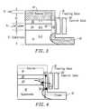
- FIG. 2is a section view of a vertical channel floating gate field effect transistor device in accordance with one embodiment of the invention.
- FIG. 3is a section view of a vertical channel floating gate field effect transistor in accordance with another embodiment of the invention.
- FIG. 4illustrates secondary electron injection in the device of FIG. 3 .
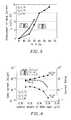
- FIG. 5is a plot of enhancement of gate current to percentage of germanium in the silicon germanium layer in the channel region.
- FIG. 6is a plot of gate current and current ratios versus lateral extent of the silicon germanium layer illustrating dependence of gate injection on the placement of the silicon germanium layer.
- FIG. 1is a section view illustrating a prior art vertical channel field effect transistor device comprising a P-doped silicon substrate 10 in which an N-doped drain region 12 and an N-doped source region 14 are formed with a channel region shown generally at 16 therebetween.
- a floating gate 18is spaced from channel 16 by a gate dielectric layer, and a control gate 20 is spaced from floating gate 18 by an inter-gate dielectric such as silicon oxide.
- Channel initiated secondary electron (CHISEL) injection in the vertical channel of the deviceoccurs when channel electrons at (a) gain energy and produce primary impact ionization at the drain (b), and the resulting holes in the substrate current may produce secondary impact ionization at (c).
- the generated secondary electronscan form a secondary electron gate current (d) that is significantly enhanced by a negative substrate bias.
- FIG. 1The structure of FIG. 1 is formed by etching a trench, mesa, or pillar in substrate 10 and then forming floating gate 18 over a gate dielectric on the sidewall. Drain 12 and source 14 are then formed by ion implantation, and gate 20 is then formed over an inter-gate dielectric on the floating gate 18 .
- the length of the channelis determined by depth of the trench, mesa or pillar.
- FIG. 2is a section view of a vertical channel FET transistor with floating gate and control gate in accordance with one embodiment of the invention.
- a Si x Ge 1 ⁇ x layer 24is epitaxially grown on the surface of substrate 10 and then a silicon layer 26 is epitaxially grown on the top of the silicon germanium layer.
- a trench, mesa, pillar, or like structureis formed by etching to expose a sidewall including the SiGe layer 24 , and then gate oxide is formed over the sidewall and floating gate 18 of doped polysilicon, for example, is then formed.
- Drain 12 and source 14are then formed by ion implantation, an inter-gate dielectric is formed over floating gate 18 , and then control gate 20 is formed by a second doped polysilicon layer, for example.
- the silicon germanium layer 24is compressively strained with the Si x Ge 1 ⁇ x layer of uniform composition or the mole fraction 1 ⁇ x may be graded. The whole layer is kept below a critical thickness and maintains pseudomorphic strain.
- FIG. 3is a section view illustrating another embodiment of the floating gate field effect transistor device in accordance with the invention in which an additional thin layer 30 of silicon is epitaxially grown on the sidewall over the exposed SiGe layer substrate 10 and silicon layer 26 .
- Silicon layer 30serves as a cap layer for the channel region of the transistor.
- Silicon layer 30is strained with an unusual configuration in which all three sides of the unit cell are different lengths, which is called orthorhombic strain.
- a gate dielectricis grown or deposited over the exposed sidewall, the floating gate material is deposited and patterned, an inter-gate dielectric is grown or deposited, the drain 12 and source 14 are formed by ion implantation, and a control gate material is deposited over an inter-gate dielectric.
- FIG. 4is a section view of the device of FIG. 3 and illustrates enhancement of the secondary electron injection mechanism in the transistor in accordance with the invention.
- Channel electrons (a)produce primary impact ionization (b) in the silicon drain region, and the resulting holes gain energy in the silicon region 30 and produce secondary electron injection in the SiGe layer 24 .
- the secondary electronsthen may be injected into the floating gate (d) as the holes escape into the negatively biased substrate 10 .
- the heterostructure formed with the silicon germanium alloy layer 24enhances secondary electron injection gate current since the silicon germanium bandgap is smaller and the energy needed to create electron hole pairs can be smaller.
- the lower threshold for impact ionization in the SiGe layerproduces more secondary electrons closer to the Si—SiO 2 than a device without the alloy layer.
- the holes generated by primary impact ionization in the drain and traveling toward the substrategain additional energy from the valence band offset at the heterostructure interface and therefore are more likely to produce a greater amount of secondary electron injection closer to the Si—SiO 2 surface near the floating gate.
- Simulation of the channel initiated secondary electron injectionindicates an enhanced gate current with the device in accordance with the invention.
- a multiple stage Monte Carlo simulation method(IEEE IEDM Technology Digest, p. 889, 1998) was modified with simple models to account for Si x Ge 1 ⁇ x offsets, and scattering mechanisms. Devices with 0.18 ⁇ m gate lengths were simulated. The devices were simulated with uniform substrate doping of 6 ⁇ 10 17 cm ⁇ 3 thin 40 ⁇ gate oxides, and shallow drain junctions (50 nm) that had lateral junctions 25 nm away from the beginning of the Si x Ge 1 ⁇ x layer.
- Si x Ge 1 ⁇ x critical layer thicknesses120, 60, 20, 10, and 5 nm were assumed for uniform mole fractions, x, of 20, 30,40,50, and 60%, respectively.
- Deviceswere simulated with and without a 15 nm Si cap thickness. These devices were simulated with 1.8 V on the gate, 2.7 V on the drain, and ⁇ 2.7 V on the substrate.
- the Si x Ge 1 ⁇ x flash devicesshowed improved gate injection up to 4.7 times (FIG. 5 ).
- an analysis of the injection mechanismshowed that the majority (84%) of the CHISEL injection was formed by secondary electrons originating in the Si x Ge 1 ⁇ x layer.
- the silicon germanium epitaxial layer in the vertical channel field effect transistor in accordance with the inventionprovides better device characteristics as cell size scales down.
- the offset in the valence band of the alloy layergives holes in the substrate current a greater energy to produce secondary impact ionization and has a smaller bandgap which further enhances impact ionization.
- the alloy layercan be optimized in position and thickness to better control the programming gate current as illustrated in FIG. 6 .
- dependence on the gate injection on the placement of Si x Ge 1 ⁇ x layeris illustrated by a solid line.
- the Ge mole fraction layer of the layeris 0.4.
- the ratios of total primary to secondary impact ionization (circles) and gate current to total secondary impact ionization (triangles)are also shown.
- the alloy layerredirects substrate current away from the source junction, thus preventing the injection of holes that can initiate bipolar breakdown.
- the separate silicon cap grown on the sidewallcan be separately engineered from the region where secondary electrons are created.
- the sidewall silicon regioncan be orthorhombically strained and have higher mobility in the channel direction as a higher saturation velocity, thus giving the device higher read currents as well as producing impact ionization in the drain at lower voltages. Since alloy scattering has been theoretically seen to prevent the enhancement of impact ionization in SiGe alloys, the provision of the silicon cap layer alloys holes to gain energy before they cross into the SiGe layer. Thus, holes accelerate in the silicon region but produce the silicon impact ionization in the separate silicon germanium alloy region.
- the heterostructuresolves some problems of flash memory arrays as size and voltages are scaled. At lower drain voltages, channel hot electron (CHE) programming becomes less effective, but the structure in accordance with the invention allows secondary electron injection to be used instead. In addition, leakage currents become magnified as more devices are included in larger arrays, but the lower voltages and the substrate voltage used in the invention produce less leakage current during programming.
- CHEchannel hot electron
- the strained heterostructure layersadd some complexity to the fabrication process since the epitaxial layers require more processing. However, these additional steps are taken at the beginning of the process flow, and as strained layer technology becomes widespread, such steps will become routine. An important limitation is that the subsequent thermal budget should be restricted to avoid relaxation in the metastable strained SiGe alloy layer.
Landscapes
- Non-Volatile Memory (AREA)
- Semiconductor Memories (AREA)
- Insulated Gate Type Field-Effect Transistor (AREA)
Abstract
Description
Claims (20)
Priority Applications (3)
| Application Number | Priority Date | Filing Date | Title |
|---|---|---|---|
| US09/596,006US6313487B1 (en) | 2000-06-15 | 2000-06-15 | Vertical channel floating gate transistor having silicon germanium channel layer |
| PCT/US2001/019273WO2001097292A1 (en) | 2000-06-15 | 2001-06-15 | Vertical channel floating gate transistor having silicon germanium channel layer |
| AU2001269858AAU2001269858A1 (en) | 2000-06-15 | 2001-06-15 | Vertical channel floating gate transistor having silicon germanium channel layer |
Applications Claiming Priority (1)
| Application Number | Priority Date | Filing Date | Title |
|---|---|---|---|
| US09/596,006US6313487B1 (en) | 2000-06-15 | 2000-06-15 | Vertical channel floating gate transistor having silicon germanium channel layer |
Publications (1)
| Publication Number | Publication Date |
|---|---|
| US6313487B1true US6313487B1 (en) | 2001-11-06 |
Family
ID=24385618
Family Applications (1)
| Application Number | Title | Priority Date | Filing Date |
|---|---|---|---|
| US09/596,006Expired - LifetimeUS6313487B1 (en) | 2000-06-15 | 2000-06-15 | Vertical channel floating gate transistor having silicon germanium channel layer |
Country Status (3)
| Country | Link |
|---|---|
| US (1) | US6313487B1 (en) |
| AU (1) | AU2001269858A1 (en) |
| WO (1) | WO2001097292A1 (en) |
Cited By (33)
| Publication number | Priority date | Publication date | Assignee | Title |
|---|---|---|---|---|
| US6580124B1 (en)* | 2000-08-14 | 2003-06-17 | Matrix Semiconductor Inc. | Multigate semiconductor device with vertical channel current and method of fabrication |
| US20030227072A1 (en)* | 2002-06-10 | 2003-12-11 | Leonard Forbes | Output prediction logic circuits with ultra-thin vertical transistors and methods of formation |
| US20040079989A1 (en)* | 2002-10-11 | 2004-04-29 | Nissan Motor Co., Ltd. | Insulated gate tunnel-injection device having heterojunction and method for manufacturing the same |
| KR100458595B1 (en)* | 2002-12-05 | 2004-12-03 | 아남반도체 주식회사 | Non-volatile memory and fabrication method thereof |
| US20050050971A1 (en)* | 2003-01-06 | 2005-03-10 | Horning Robert D. | Methods and structure for improving wafer bow control |
| KR100472008B1 (en)* | 2002-12-05 | 2005-03-10 | 동부아남반도체 주식회사 | Non-volatile memory and fabrication method thereof |
| KR100472009B1 (en)* | 2002-12-05 | 2005-03-10 | 동부아남반도체 주식회사 | Non-volatile memory and fabrication method thereof |
| US20050201150A1 (en)* | 2003-06-06 | 2005-09-15 | Chih-Hsin Wang | Method and apparatus for semiconductor device and semiconductor memory device |
| US20050276117A1 (en)* | 2004-05-26 | 2005-12-15 | Micron Technology, Inc. | Ballistic direct injection flash memory cell on strained silicon structures |
| US20060008960A1 (en)* | 2004-07-09 | 2006-01-12 | Chaudhry Muhammad I | Fabrication of an EEPROM cell with SiGe source/drain regions |
| US20060017091A1 (en)* | 2004-07-01 | 2006-01-26 | Chih-Hsin Wang | Method and apparatus for nonvolatile memory |
| US20060186456A1 (en)* | 2005-02-18 | 2006-08-24 | Burnett James D | NVM cell on SOI and method of manufacture |
| US20060249783A1 (en)* | 2005-05-06 | 2006-11-09 | Bohumil Lojek | Ultrascalable vertical MOS transistor with planar contacts |
| US20060289924A1 (en)* | 2005-06-28 | 2006-12-28 | Chih-Hsin Wang | Low power electrically alterable nonvolatile memory cells and arrays |
| US20070087550A1 (en)* | 2004-05-18 | 2007-04-19 | Atmel Corporation | Low-voltage single-layer polysilicon eeprom memory cell |
| US20070281425A1 (en)* | 2003-06-06 | 2007-12-06 | Chih-Hsin Wang | Method and apparatus transporting charges in semiconductor device and semiconductor memory device |
| CN100365819C (en)* | 2005-12-06 | 2008-01-30 | 北京大学 | A kind of flash memory structure and preparation method thereof |
| US7352631B2 (en) | 2005-02-18 | 2008-04-01 | Freescale Semiconductor, Inc. | Methods for programming a floating body nonvolatile memory |
| US20080179636A1 (en)* | 2007-01-27 | 2008-07-31 | International Business Machines Corporation | N-fets with tensilely strained semiconductor channels, and method for fabricating same using buried pseudomorphic layers |
| US20080296652A1 (en)* | 2004-05-18 | 2008-12-04 | Leonard Forbes | Split gate flash memory cell with ballistic injection |
| US20090236657A1 (en)* | 2008-03-24 | 2009-09-24 | Micron Technology, Inc. | Impact ionization devices and methods of making the same |
| US7613041B2 (en) | 2003-06-06 | 2009-11-03 | Chih-Hsin Wang | Methods for operating semiconductor device and semiconductor memory device |
| US7759719B2 (en) | 2004-07-01 | 2010-07-20 | Chih-Hsin Wang | Electrically alterable memory cell |
| US8072023B1 (en) | 2007-11-12 | 2011-12-06 | Marvell International Ltd. | Isolation for non-volatile memory cell array |
| US8120088B1 (en) | 2007-12-07 | 2012-02-21 | Marvell International Ltd. | Non-volatile memory cell and array |
| WO2012051824A1 (en)* | 2010-10-22 | 2012-04-26 | 北京大学 | Flash memory and fabricating and operating method thereof |
| CN102623505A (en)* | 2012-04-01 | 2012-08-01 | 北京大学 | Radiation resistant transistor based on vertical double gate and its preparation method |
| US8431961B2 (en) | 2011-02-03 | 2013-04-30 | Micron Technology, Inc. | Memory devices with a connecting region having a band gap lower than a band gap of a body region |
| US9466731B2 (en)* | 2014-08-12 | 2016-10-11 | Empire Technology Development Llc | Dual channel memory |
| US10020317B2 (en) | 2015-08-31 | 2018-07-10 | Cypress Semiconductor Corporation | Memory device with multi-layer channel and charge trapping layer |
| US10515801B2 (en) | 2007-06-04 | 2019-12-24 | Micron Technology, Inc. | Pitch multiplication using self-assembling materials |
| US10923493B2 (en) | 2018-09-06 | 2021-02-16 | Micron Technology, Inc. | Microelectronic devices, electronic systems, and related methods |
| US11557663B2 (en)* | 2017-08-29 | 2023-01-17 | International Business Machines Corporation | Twin gate tunnel field-effect transistor (FET) |
Families Citing this family (1)
| Publication number | Priority date | Publication date | Assignee | Title |
|---|---|---|---|---|
| CN110416085A (en)* | 2019-07-10 | 2019-11-05 | 复旦大学 | Semi-floating gate transistor with SiGe channel structure and manufacturing method thereof |
Citations (27)
| Publication number | Priority date | Publication date | Assignee | Title |
|---|---|---|---|---|
| US4499557A (en) | 1980-10-28 | 1985-02-12 | Energy Conversion Devices, Inc. | Programmable cell for use in programmable electronic arrays |
| US4599705A (en) | 1979-12-13 | 1986-07-08 | Energy Conversion Devices, Inc. | Programmable cell for use in programmable electronic arrays |
| US4870470A (en) | 1987-10-16 | 1989-09-26 | International Business Machines Corporation | Non-volatile memory cell having Si rich silicon nitride charge trapping layer |
| US5162880A (en) | 1989-09-27 | 1992-11-10 | Kabushiki Kaisha Toshiba | Nonvolatile memory cell having gate insulation film with carrier traps therein |
| US5272365A (en)* | 1990-03-29 | 1993-12-21 | Kabushiki Kaisha Toshiba | Silicon transistor device with silicon-germanium electron gas hetero structure channel |
| US5334855A (en) | 1992-08-24 | 1994-08-02 | Motorola, Inc. | Diamond/phosphor polycrystalline led and display |
| US5341328A (en) | 1991-01-18 | 1994-08-23 | Energy Conversion Devices, Inc. | Electrically erasable memory elements having reduced switching current requirements and increased write/erase cycle life |
| US5349209A (en) | 1992-07-30 | 1994-09-20 | Motorola, Inc. | Diamond/organic LED |
| US5432356A (en) | 1993-04-02 | 1995-07-11 | Fujitsu Limited | Semiconductor heterojunction floating layer memory device and method for storing information in the same |
| US5451800A (en)* | 1992-12-02 | 1995-09-19 | International Business Machines Corporation | Metal oxide semiconductor heterojunction field effect transistor (MOSHFET) |
| US5534712A (en) | 1991-01-18 | 1996-07-09 | Energy Conversion Devices, Inc. | Electrically erasable memory elements characterized by reduced current and improved thermal stability |
| US5534713A (en)* | 1994-05-20 | 1996-07-09 | International Business Machines Corporation | Complementary metal-oxide semiconductor transistor logic using strained SI/SIGE heterostructure layers |
| US5546340A (en) | 1995-06-13 | 1996-08-13 | Advanced Micro Devices, Inc. | Non-volatile memory array with over-erase correction |
| US5659504A (en) | 1995-05-25 | 1997-08-19 | Lucent Technologies Inc. | Method and apparatus for hot carrier injection |
| US5698869A (en) | 1994-09-13 | 1997-12-16 | Kabushiki Kaisha Toshiba | Insulated-gate transistor having narrow-bandgap-source |
| US5801396A (en) | 1989-01-18 | 1998-09-01 | Stmicroelectronics, Inc. | Inverted field-effect device with polycrystalline silicon/germanium channel |
| US5818761A (en) | 1996-09-10 | 1998-10-06 | Mitsubishi Denki Kabushiki Kaisha | Non-volatile semiconductor memory device capable of high speed programming/erasure |
| US5821577A (en)* | 1991-01-10 | 1998-10-13 | International Business Machines Corporation | Graded channel field effect transistor |
| US5901084A (en) | 1997-03-10 | 1999-05-04 | Mitsubishi Denki Kabushiki Kaisha | Nonvolatile semiconductor memory device having floating gate electrode |
| US5926414A (en) | 1997-04-04 | 1999-07-20 | Magnetic Semiconductors | High-efficiency miniature magnetic integrated circuit structures |
| US5969384A (en)* | 1996-06-08 | 1999-10-19 | United Microelectronics Corp. | Flash memory having separate data programming and erasing terminals |
| US5986581A (en) | 1998-01-13 | 1999-11-16 | The United States Of America As Represented By The Secretary Of The Air Force | Programmable infrared marker (PIRM) |
| US5991200A (en) | 1989-02-06 | 1999-11-23 | Hitachi, Ltd. | Nonvolatile semiconductor memory device |
| US6013950A (en) | 1994-05-19 | 2000-01-11 | Sandia Corporation | Semiconductor diode with external field modulation |
| US6031263A (en) | 1997-07-29 | 2000-02-29 | Micron Technology, Inc. | DEAPROM and transistor with gallium nitride or gallium aluminum nitride gate |
| US6204123B1 (en)* | 1998-10-30 | 2001-03-20 | Sony Corporation | Vertical floating gate transistor with epitaxial channel |
| US6207978B1 (en)* | 2000-03-01 | 2001-03-27 | Advanced Micro Devices, Inc. | Flash memory cells having a modulation doped heterojunction structure |
- 2000
- 2000-06-15USUS09/596,006patent/US6313487B1/ennot_activeExpired - Lifetime
- 2001
- 2001-06-15AUAU2001269858Apatent/AU2001269858A1/ennot_activeAbandoned
- 2001-06-15WOPCT/US2001/019273patent/WO2001097292A1/enactiveApplication Filing
Patent Citations (28)
| Publication number | Priority date | Publication date | Assignee | Title |
|---|---|---|---|---|
| US4599705A (en) | 1979-12-13 | 1986-07-08 | Energy Conversion Devices, Inc. | Programmable cell for use in programmable electronic arrays |
| US4499557A (en) | 1980-10-28 | 1985-02-12 | Energy Conversion Devices, Inc. | Programmable cell for use in programmable electronic arrays |
| US4870470A (en) | 1987-10-16 | 1989-09-26 | International Business Machines Corporation | Non-volatile memory cell having Si rich silicon nitride charge trapping layer |
| US5801396A (en) | 1989-01-18 | 1998-09-01 | Stmicroelectronics, Inc. | Inverted field-effect device with polycrystalline silicon/germanium channel |
| US5821136A (en) | 1989-01-18 | 1998-10-13 | Stmicroelectronics, Inc. | Inverted field-effect device with polycrystalline silicon/germanium channel |
| US5991200A (en) | 1989-02-06 | 1999-11-23 | Hitachi, Ltd. | Nonvolatile semiconductor memory device |
| US5162880A (en) | 1989-09-27 | 1992-11-10 | Kabushiki Kaisha Toshiba | Nonvolatile memory cell having gate insulation film with carrier traps therein |
| US5272365A (en)* | 1990-03-29 | 1993-12-21 | Kabushiki Kaisha Toshiba | Silicon transistor device with silicon-germanium electron gas hetero structure channel |
| US5821577A (en)* | 1991-01-10 | 1998-10-13 | International Business Machines Corporation | Graded channel field effect transistor |
| US5341328A (en) | 1991-01-18 | 1994-08-23 | Energy Conversion Devices, Inc. | Electrically erasable memory elements having reduced switching current requirements and increased write/erase cycle life |
| US5534712A (en) | 1991-01-18 | 1996-07-09 | Energy Conversion Devices, Inc. | Electrically erasable memory elements characterized by reduced current and improved thermal stability |
| US5349209A (en) | 1992-07-30 | 1994-09-20 | Motorola, Inc. | Diamond/organic LED |
| US5334855A (en) | 1992-08-24 | 1994-08-02 | Motorola, Inc. | Diamond/phosphor polycrystalline led and display |
| US5451800A (en)* | 1992-12-02 | 1995-09-19 | International Business Machines Corporation | Metal oxide semiconductor heterojunction field effect transistor (MOSHFET) |
| US5432356A (en) | 1993-04-02 | 1995-07-11 | Fujitsu Limited | Semiconductor heterojunction floating layer memory device and method for storing information in the same |
| US6013950A (en) | 1994-05-19 | 2000-01-11 | Sandia Corporation | Semiconductor diode with external field modulation |
| US5534713A (en)* | 1994-05-20 | 1996-07-09 | International Business Machines Corporation | Complementary metal-oxide semiconductor transistor logic using strained SI/SIGE heterostructure layers |
| US5698869A (en) | 1994-09-13 | 1997-12-16 | Kabushiki Kaisha Toshiba | Insulated-gate transistor having narrow-bandgap-source |
| US5659504A (en) | 1995-05-25 | 1997-08-19 | Lucent Technologies Inc. | Method and apparatus for hot carrier injection |
| US5546340A (en) | 1995-06-13 | 1996-08-13 | Advanced Micro Devices, Inc. | Non-volatile memory array with over-erase correction |
| US5969384A (en)* | 1996-06-08 | 1999-10-19 | United Microelectronics Corp. | Flash memory having separate data programming and erasing terminals |
| US5818761A (en) | 1996-09-10 | 1998-10-06 | Mitsubishi Denki Kabushiki Kaisha | Non-volatile semiconductor memory device capable of high speed programming/erasure |
| US5901084A (en) | 1997-03-10 | 1999-05-04 | Mitsubishi Denki Kabushiki Kaisha | Nonvolatile semiconductor memory device having floating gate electrode |
| US5926414A (en) | 1997-04-04 | 1999-07-20 | Magnetic Semiconductors | High-efficiency miniature magnetic integrated circuit structures |
| US6031263A (en) | 1997-07-29 | 2000-02-29 | Micron Technology, Inc. | DEAPROM and transistor with gallium nitride or gallium aluminum nitride gate |
| US5986581A (en) | 1998-01-13 | 1999-11-16 | The United States Of America As Represented By The Secretary Of The Air Force | Programmable infrared marker (PIRM) |
| US6204123B1 (en)* | 1998-10-30 | 2001-03-20 | Sony Corporation | Vertical floating gate transistor with epitaxial channel |
| US6207978B1 (en)* | 2000-03-01 | 2001-03-27 | Advanced Micro Devices, Inc. | Flash memory cells having a modulation doped heterojunction structure |
Cited By (69)
| Publication number | Priority date | Publication date | Assignee | Title |
|---|---|---|---|---|
| US6677204B2 (en) | 2000-08-14 | 2004-01-13 | Matrix Semiconductor, Inc. | Multigate semiconductor device with vertical channel current and method of fabrication |
| US6580124B1 (en)* | 2000-08-14 | 2003-06-17 | Matrix Semiconductor Inc. | Multigate semiconductor device with vertical channel current and method of fabrication |
| US7217974B2 (en) | 2002-06-10 | 2007-05-15 | Micron Technology, Inc. | Output prediction logic circuits with ultra-thin vertical transistors and methods of formation |
| US20050156230A1 (en)* | 2002-06-10 | 2005-07-21 | Leonard Forbes | Output prediction logic circuits with ultra-thin vertical transistors and methods of formation |
| US20040147079A1 (en)* | 2002-06-10 | 2004-07-29 | Leonard Forbes | Output prediction logic circuits with ultra-thin vertical transistors and methods of formation |
| US20030227072A1 (en)* | 2002-06-10 | 2003-12-11 | Leonard Forbes | Output prediction logic circuits with ultra-thin vertical transistors and methods of formation |
| US6998311B2 (en) | 2002-06-10 | 2006-02-14 | Micron Technology, Inc. | Methods of forming output prediction logic circuits with ultra-thin vertical transistors |
| US6900521B2 (en)* | 2002-06-10 | 2005-05-31 | Micron Technology, Inc. | Vertical transistors and output prediction logic circuits containing same |
| US20040079989A1 (en)* | 2002-10-11 | 2004-04-29 | Nissan Motor Co., Ltd. | Insulated gate tunnel-injection device having heterojunction and method for manufacturing the same |
| US7217950B2 (en)* | 2002-10-11 | 2007-05-15 | Nissan Motor Co., Ltd. | Insulated gate tunnel-injection device having heterojunction and method for manufacturing the same |
| KR100472008B1 (en)* | 2002-12-05 | 2005-03-10 | 동부아남반도체 주식회사 | Non-volatile memory and fabrication method thereof |
| KR100472009B1 (en)* | 2002-12-05 | 2005-03-10 | 동부아남반도체 주식회사 | Non-volatile memory and fabrication method thereof |
| KR100458595B1 (en)* | 2002-12-05 | 2004-12-03 | 아남반도체 주식회사 | Non-volatile memory and fabrication method thereof |
| US20050050971A1 (en)* | 2003-01-06 | 2005-03-10 | Horning Robert D. | Methods and structure for improving wafer bow control |
| US20050201150A1 (en)* | 2003-06-06 | 2005-09-15 | Chih-Hsin Wang | Method and apparatus for semiconductor device and semiconductor memory device |
| US20080070390A1 (en)* | 2003-06-06 | 2008-03-20 | Chih-Hsin Wang | Method and apparatus for semiconductor device and semiconductor memory device |
| US7824981B2 (en) | 2003-06-06 | 2010-11-02 | Chih-Hsin Wang | Method and apparatus for semiconductor device and semiconductor memory device |
| US7550800B2 (en) | 2003-06-06 | 2009-06-23 | Chih-Hsin Wang | Method and apparatus transporting charges in semiconductor device and semiconductor memory device |
| US7613041B2 (en) | 2003-06-06 | 2009-11-03 | Chih-Hsin Wang | Methods for operating semiconductor device and semiconductor memory device |
| US7745286B2 (en) | 2003-06-06 | 2010-06-29 | Chih-Hsin Wang | Methods of forming semiconductor devices |
| US7741177B2 (en) | 2003-06-06 | 2010-06-22 | Chih-Hsin Wang | Method and apparatus transporting charges in semiconductor device and semiconductor memory device |
| US20070281425A1 (en)* | 2003-06-06 | 2007-12-06 | Chih-Hsin Wang | Method and apparatus transporting charges in semiconductor device and semiconductor memory device |
| US20070087550A1 (en)* | 2004-05-18 | 2007-04-19 | Atmel Corporation | Low-voltage single-layer polysilicon eeprom memory cell |
| US20070133301A1 (en)* | 2004-05-18 | 2007-06-14 | Atmel Corporation | Low-voltage single-layer polysilicon eeprom memory cell |
| US7697328B2 (en)* | 2004-05-18 | 2010-04-13 | Micron Technology, Inc. | Split gate flash memory cell with ballistic injection |
| US7408812B2 (en) | 2004-05-18 | 2008-08-05 | Atmel Corporation | Low-voltage single-layer polysilicon EEPROM memory cell |
| US20080296652A1 (en)* | 2004-05-18 | 2008-12-04 | Leonard Forbes | Split gate flash memory cell with ballistic injection |
| US7221597B2 (en) | 2004-05-26 | 2007-05-22 | Micron Technology, Inc. | Ballistic direct injection flash memory cell on strained silicon structures |
| US20050276117A1 (en)* | 2004-05-26 | 2005-12-15 | Micron Technology, Inc. | Ballistic direct injection flash memory cell on strained silicon structures |
| US7759719B2 (en) | 2004-07-01 | 2010-07-20 | Chih-Hsin Wang | Electrically alterable memory cell |
| US7115942B2 (en) | 2004-07-01 | 2006-10-03 | Chih-Hsin Wang | Method and apparatus for nonvolatile memory |
| US20060017091A1 (en)* | 2004-07-01 | 2006-01-26 | Chih-Hsin Wang | Method and apparatus for nonvolatile memory |
| US7091075B2 (en) | 2004-07-09 | 2006-08-15 | Atmel Corporation | Fabrication of an EEPROM cell with SiGe source/drain regions |
| US20060244073A1 (en)* | 2004-07-09 | 2006-11-02 | Atmel Corporation | FABRICATION OF AN EEPROM CELL WITH SiGe SOURCE/DRAIN REGIONS |
| US20060008960A1 (en)* | 2004-07-09 | 2006-01-12 | Chaudhry Muhammad I | Fabrication of an EEPROM cell with SiGe source/drain regions |
| CN100492615C (en)* | 2004-07-09 | 2009-05-27 | 爱特梅尔公司 | Fabrication of EEPROM cell with SiGe source/drain regions |
| US7352631B2 (en) | 2005-02-18 | 2008-04-01 | Freescale Semiconductor, Inc. | Methods for programming a floating body nonvolatile memory |
| US20060186456A1 (en)* | 2005-02-18 | 2006-08-24 | Burnett James D | NVM cell on SOI and method of manufacture |
| US20060249783A1 (en)* | 2005-05-06 | 2006-11-09 | Bohumil Lojek | Ultrascalable vertical MOS transistor with planar contacts |
| US7335943B2 (en)* | 2005-05-06 | 2008-02-26 | Atmel Corporation | Ultrascalable vertical MOS transistor with planar contacts |
| US20060289924A1 (en)* | 2005-06-28 | 2006-12-28 | Chih-Hsin Wang | Low power electrically alterable nonvolatile memory cells and arrays |
| US7719050B1 (en) | 2005-06-28 | 2010-05-18 | Chih-Hsin Wang | Low power electrically alterable nonvolatile memory cells and arrays |
| US7547601B2 (en) | 2005-06-28 | 2009-06-16 | Marvell World Trade Ltd. | Low power electrically alterable nonvolatile memory cells and arrays |
| US7411244B2 (en) | 2005-06-28 | 2008-08-12 | Chih-Hsin Wang | Low power electrically alterable nonvolatile memory cells and arrays |
| CN100365819C (en)* | 2005-12-06 | 2008-01-30 | 北京大学 | A kind of flash memory structure and preparation method thereof |
| US20080179636A1 (en)* | 2007-01-27 | 2008-07-31 | International Business Machines Corporation | N-fets with tensilely strained semiconductor channels, and method for fabricating same using buried pseudomorphic layers |
| US10515801B2 (en) | 2007-06-04 | 2019-12-24 | Micron Technology, Inc. | Pitch multiplication using self-assembling materials |
| US8072023B1 (en) | 2007-11-12 | 2011-12-06 | Marvell International Ltd. | Isolation for non-volatile memory cell array |
| US8120088B1 (en) | 2007-12-07 | 2012-02-21 | Marvell International Ltd. | Non-volatile memory cell and array |
| US20090236657A1 (en)* | 2008-03-24 | 2009-09-24 | Micron Technology, Inc. | Impact ionization devices and methods of making the same |
| US9373716B2 (en) | 2008-03-24 | 2016-06-21 | Micron Technology, Inc. | Impact ionization devices, and methods of forming impact ionization devices |
| US8674434B2 (en)* | 2008-03-24 | 2014-03-18 | Micron Technology, Inc. | Impact ionization devices |
| WO2012051824A1 (en)* | 2010-10-22 | 2012-04-26 | 北京大学 | Flash memory and fabricating and operating method thereof |
| CN102456745A (en)* | 2010-10-22 | 2012-05-16 | 北京大学 | Flash memory as well as preparation method and operation method thereof |
| US8526242B2 (en) | 2010-10-22 | 2013-09-03 | Peking University | Flash memory and fabrication method and operation method for the same |
| US9640260B2 (en)* | 2011-02-03 | 2017-05-02 | Micron Technology, Inc. | Memory devices with a connecting region having a band gap lower than a band gap of a body region |
| US20140313833A1 (en)* | 2011-02-03 | 2014-10-23 | Micron Technology, Inc. | Memory devices with a connecting region having a band gap lower than a band gap of a body region |
| US8766320B2 (en) | 2011-02-03 | 2014-07-01 | Micron Technology, Inc. | Memory devices with a connecting region having a band gap lower than a band gap of a body region |
| US8431961B2 (en) | 2011-02-03 | 2013-04-30 | Micron Technology, Inc. | Memory devices with a connecting region having a band gap lower than a band gap of a body region |
| US9953710B2 (en) | 2011-02-03 | 2018-04-24 | Micron Technology, Inc. | Memory devices with a connecting region having a band gap lower than a band gap of a body region |
| CN102623505B (en)* | 2012-04-01 | 2014-07-02 | 北京大学 | Vertical dual-gate-based anti-radiation transistor and manufacturing method thereof |
| CN102623505A (en)* | 2012-04-01 | 2012-08-01 | 北京大学 | Radiation resistant transistor based on vertical double gate and its preparation method |
| US9997640B2 (en) | 2014-08-12 | 2018-06-12 | Empire Technology Development Llc | Dual channel memory |
| US9466731B2 (en)* | 2014-08-12 | 2016-10-11 | Empire Technology Development Llc | Dual channel memory |
| US10020317B2 (en) | 2015-08-31 | 2018-07-10 | Cypress Semiconductor Corporation | Memory device with multi-layer channel and charge trapping layer |
| US11557663B2 (en)* | 2017-08-29 | 2023-01-17 | International Business Machines Corporation | Twin gate tunnel field-effect transistor (FET) |
| US10923493B2 (en) | 2018-09-06 | 2021-02-16 | Micron Technology, Inc. | Microelectronic devices, electronic systems, and related methods |
| US11778824B2 (en) | 2018-09-06 | 2023-10-03 | Micron Technology, Inc. | Apparatuses including band offset materials, and related systems |
| US12342544B2 (en) | 2018-09-06 | 2025-06-24 | Lodestar Licensing Group, Llc | Apparatuses including band offset materials, and related memory devices |
Also Published As
| Publication number | Publication date |
|---|---|
| WO2001097292A1 (en) | 2001-12-20 |
| AU2001269858A1 (en) | 2001-12-24 |
Similar Documents
| Publication | Publication Date | Title |
|---|---|---|
| US6313487B1 (en) | Vertical channel floating gate transistor having silicon germanium channel layer | |
| US6313486B1 (en) | Floating gate transistor having buried strained silicon germanium channel layer | |
| KR101097416B1 (en) | Recess channel flash architecture for reduced short channel effects | |
| JP4439593B2 (en) | Fermi threshold field effect transistor and method of manufacturing the same | |
| US6617643B1 (en) | Low power tunneling metal-oxide-semiconductor (MOS) device | |
| US7332386B2 (en) | Methods of fabricating fin field transistors | |
| US6734063B2 (en) | Non-volatile memory cell and fabrication method | |
| US5424567A (en) | Protected programmable transistor with reduced parasitic capacitances and method of fabrication | |
| US7838401B2 (en) | Semiconductor device and manufacturing method thereof | |
| US8466505B2 (en) | Multi-level flash memory cell capable of fast programming | |
| US20050239254A1 (en) | Quasi-plannar and FinFET-like transistors on bulk silicon | |
| US20090184369A1 (en) | Finfet devices and methods for manufacturing the same | |
| JPH1065162A (en) | Insulated gate semiconductor device and method of manufacturing the same | |
| US6963108B1 (en) | Recessed channel | |
| US6207978B1 (en) | Flash memory cells having a modulation doped heterojunction structure | |
| US6605845B1 (en) | Asymmetric MOSFET using spacer gate technique | |
| US6180502B1 (en) | Self-aligned process for making asymmetric MOSFET using spacer gate technique | |
| US20110284934A1 (en) | Semiconductor device and method of fabricating the same | |
| US6475863B1 (en) | Method for fabricating self-aligned gate of flash memory cell | |
| CN104701263B (en) | A kind of manufacture method of half floating-gate device | |
| US5672524A (en) | Three-dimensional complementary field effect transistor process | |
| CN112002694B (en) | SONOS memory and its manufacturing method | |
| US7030465B2 (en) | Semiconductor device that can increase the carrier mobility and method for fabricating the same | |
| Banerjee et al. | Vertical channel floating gate transistor having silicon germanium channel layer | |
| US6646326B1 (en) | Method and system for providing source/drain-gate spatial overlap engineering for low-power devices |
Legal Events
| Date | Code | Title | Description |
|---|---|---|---|
| AS | Assignment | Owner name:BOARD OF REGENTS, THE UNIVERSITY OF TEXAS SYSTEM, Free format text:ASSIGNMENT OF ASSIGNORS INTEREST;ASSIGNORS:KENCKE, DAVID L.;BANERJEE, SANJAY K.;REEL/FRAME:010911/0259;SIGNING DATES FROM 20000607 TO 20000612 | |
| STCF | Information on status: patent grant | Free format text:PATENTED CASE | |
| FPAY | Fee payment | Year of fee payment:4 | |
| AS | Assignment | Owner name:INTELLECTUAL VENTURES HOLDING 40 LLC, NEVADA Free format text:ASSIGNMENT OF ASSIGNORS INTEREST;ASSIGNOR:THE BOARD OF REGENTS, THE UNIVERSITY OF TEXAS SYSTEM;REEL/FRAME:020919/0506 Effective date:20080411 Owner name:INTELLECTUAL VENTURES HOLDING 40 LLC,NEVADA Free format text:ASSIGNMENT OF ASSIGNORS INTEREST;ASSIGNOR:THE BOARD OF REGENTS, THE UNIVERSITY OF TEXAS SYSTEM;REEL/FRAME:020919/0506 Effective date:20080411 | |
| FPAY | Fee payment | Year of fee payment:8 | |
| FPAY | Fee payment | Year of fee payment:12 | |
| AS | Assignment | Owner name:INTELLECTUAL VENTURES ASSETS 157 LLC, DELAWARE Free format text:ASSIGNMENT OF ASSIGNORS INTEREST;ASSIGNOR:INTELLECTUAL VENTURES HOLDING 40 LLC;REEL/FRAME:051411/0527 Effective date:20191223 | |
| AS | Assignment | Owner name:LIBERTY PATENTS LLC, TEXAS Free format text:ASSIGNMENT OF ASSIGNORS INTEREST;ASSIGNOR:INTELLECTUAL VENTURES ASSETS 157 LLC;REEL/FRAME:051630/0115 Effective date:20191230 |