US6313486B1 - Floating gate transistor having buried strained silicon germanium channel layer - Google Patents
Floating gate transistor having buried strained silicon germanium channel layerDownload PDFInfo
- Publication number
- US6313486B1 US6313486B1US09/595,366US59536600AUS6313486B1US 6313486 B1US6313486 B1US 6313486B1US 59536600 AUS59536600 AUS 59536600AUS 6313486 B1US6313486 B1US 6313486B1
- Authority
- US
- United States
- Prior art keywords
- layer
- silicon
- field effect
- effect transistor
- floating gate
- Prior art date
- Legal status (The legal status is an assumption and is not a legal conclusion. Google has not performed a legal analysis and makes no representation as to the accuracy of the status listed.)
- Expired - Lifetime
Links
- 238000007667floatingMethods0.000titleclaimsabstractdescription27
- 229910000577Silicon-germaniumInorganic materials0.000titleclaimsabstractdescription20
- LEVVHYCKPQWKOP-UHFFFAOYSA-N[Si].[Ge]Chemical compound[Si].[Ge]LEVVHYCKPQWKOP-UHFFFAOYSA-N0.000titleabstractdescription8
- XUIMIQQOPSSXEZ-UHFFFAOYSA-NSiliconChemical compound[Si]XUIMIQQOPSSXEZ-UHFFFAOYSA-N0.000claimsabstractdescription29
- 229910052710siliconInorganic materials0.000claimsabstractdescription29
- 239000010703siliconSubstances0.000claimsabstractdescription29
- 239000000758substrateSubstances0.000claimsabstractdescription26
- 229910045601alloyInorganic materials0.000claimsabstractdescription25
- 239000000956alloySubstances0.000claimsabstractdescription25
- 230000005669field effectEffects0.000claimsabstractdescription18
- 229910020751SixGe1-xInorganic materials0.000claimsdescription22
- 238000002347injectionMethods0.000claimsdescription18
- 239000007924injectionSubstances0.000claimsdescription18
- 239000004065semiconductorSubstances0.000claimsdescription5
- 229910021421monocrystalline siliconInorganic materials0.000claims1
- 229910052732germaniumInorganic materials0.000abstractdescription3
- GNPVGFCGXDBREM-UHFFFAOYSA-Ngermanium atomChemical compound[Ge]GNPVGFCGXDBREM-UHFFFAOYSA-N0.000abstractdescription3
- 230000007246mechanismEffects0.000description8
- 239000002784hot electronSubstances0.000description5
- 229910008062Si-SiO2Inorganic materials0.000description4
- 229910006403Si—SiO2Inorganic materials0.000description4
- 238000000034methodMethods0.000description3
- 238000003491arrayMethods0.000description2
- 238000010586diagramMethods0.000description2
- 238000005516engineering processMethods0.000description2
- 238000012545processingMethods0.000description2
- 238000000342Monte Carlo simulationMethods0.000description1
- 229910006990Si1-xGexInorganic materials0.000description1
- 229910007020Si1−xGexInorganic materials0.000description1
- VYPSYNLAJGMNEJ-UHFFFAOYSA-NSilicium dioxideChemical compoundO=[Si]=OVYPSYNLAJGMNEJ-UHFFFAOYSA-N0.000description1
- 229910008310Si—GeInorganic materials0.000description1
- 238000004458analytical methodMethods0.000description1
- 230000015556catabolic processEffects0.000description1
- 238000007796conventional methodMethods0.000description1
- 230000008878couplingEffects0.000description1
- 238000010168coupling processMethods0.000description1
- 238000005859coupling reactionMethods0.000description1
- 238000011161developmentMethods0.000description1
- 230000000694effectsEffects0.000description1
- 238000004519manufacturing processMethods0.000description1
- 230000006386memory functionEffects0.000description1
- 229910044991metal oxideInorganic materials0.000description1
- 150000004706metal oxidesChemical class0.000description1
- 238000012986modificationMethods0.000description1
- 230000004048modificationEffects0.000description1
- 238000001451molecular beam epitaxyMethods0.000description1
- 230000008569processEffects0.000description1
- 229910052814silicon oxideInorganic materials0.000description1
- 238000004088simulationMethods0.000description1
- 230000007704transitionEffects0.000description1
Images


Classifications
- H—ELECTRICITY
- H10—SEMICONDUCTOR DEVICES; ELECTRIC SOLID-STATE DEVICES NOT OTHERWISE PROVIDED FOR
- H10D—INORGANIC ELECTRIC SEMICONDUCTOR DEVICES
- H10D30/00—Field-effect transistors [FET]
- H10D30/60—Insulated-gate field-effect transistors [IGFET]
- H10D30/68—Floating-gate IGFETs
- H10D30/681—Floating-gate IGFETs having only two programming levels
- H10D30/684—Floating-gate IGFETs having only two programming levels programmed by hot carrier injection
- H10D30/685—Floating-gate IGFETs having only two programming levels programmed by hot carrier injection from the channel
Definitions
- This inventionrelates generally to field effect transistors, and more particularly the invention relates to insulated field effect transistors (IGFETS) and metal oxide silicon transistors (MOS) having a floating gate for use in electrically erasable, programmable read-only memory (EEPROM) cells as Flash EEPROM cells.
- IGFETSinsulated field effect transistors
- MOSmetal oxide silicon transistors
- EEPROMelectrically erasable, programmable read-only memory
- the MOS transistorhas source and drain regions separated by a channel region with the conduction of the channel region controlled by voltage biasing an overlying gate.
- the Flash EEPROM devicehas the structure of a metal-oxide-semiconductor field effect transistor (MOSFET) but additionally includes an electrically isolated gate, or floating gate, to store charge. Controlling the amount of charge on the floating gate alters the threshold voltage and creates a nonvolatile memory function. The cell is read in the same manner as a MOSFET. Flash memory development is therefore driven by some of the same concerns as MOS technology, but to the demands for scalable devices with high access times and low leakage currents, it adds the requirement of efficient, controllable gate currents, and channel hot electron (CHE) programming used in conventional flash cells. As the drain and gate voltages are lowered, however, this method becomes less efficient.
- CHEchannel hot electron
- CHISELChannel initiated secondary electron
- SCHEsubstrate current induced hot electron
- the present inventionis directed to a floating gate field effect transistor in which secondary electron injection is enhanced when programming the floating gate.
- a field effect transistorcomprises a semiconductor body having source and drain regions formed in spaced surface regions of the semiconductor.
- a channel region between the source and drain regionsincludes a compressively strained Si x Ge 1 ⁇ x alloy layer with a silicon cap layer over the alloy layer. Conduction in the channel region is controlled by a gate structure including a control gate over the channel region and a floating gate between the control gate and the channel region.
- the voltage threshold of the transistoris programmed by selectively injecting electrons from the channel region into the floating gate. Lower programming voltages are realized due to increased secondary impact ionization with the presence of the heterostructure interface in the channel and the smaller bandgap of the silicon-germanium layer.
- the Si x Ge 1 ⁇ x layeris grown on a silicon substrate with a graded mole fraction, 1 ⁇ x, increasing from 0 to a desired maximum end of growth direction. The maximum value is then maintained during the remainder of the Si x Ge 1 ⁇ x layer growth, and the whole alloy layer is kept below a critical thickness that maintains pseudomorphic strain.
- a cap layer of siliconis then epitaxially grown on top of the alloy layer that serves as a channel for the device.
- FIG. 1is a section view of a flash memory device illustrating the programming of the floating gate by primary and secondary impact ionization.
- FIG. 2is a section view of a flash memory device in accordance with one embodiment of the invention.
- FIG. 3is the section view of FIG. 2 and further illustrates the electron injection mechanism of the invention.
- FIG. 4illustrates a valence/conduction band diagram of the electron injection mechanism in accordance with the invention.
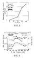
- FIG. 5is a graph of enhancement of gate current versus percentage of germanium for varying maximum mole fractions.
- FIG. 6is a graph of gate current and current ratios versus silicon cap thickness which illustrates dependence of the gate injection on the placement of the silicon germanium alloy layer.
- FIG. 1is a section view of a field effect transistor formed in a P-doped noncrystalline silicon substrate 10 having spaced N-doped source region 12 and N-doped drain region 14 with channel region 16 therebetween.
- a floating gate 18 and control gate 20are positioned above the channel region for controlling conduction thereof.
- Floating gate 18is formed on a gate silicon oxide layer
- control gate 20is formed on an intergate oxide layer.
- channel hot electron (CHE) injectionmay occur at (a) when channel electrons gain energy and are redirected into the floating gate.
- Channel electronsmay also produce primary impact ionization at the drain (b) and the resulting holes in the substrate current may produce secondary impact ionization (c).
- the generated secondary electronscan form a channel-initiated secondary electron (CHISEL) gate current at (d) that is significantly enhanced by a negative substrate bias.
- CHISELchannel-initiated secondary electron
- FIG. 2is a section view of a field effect transistor having a floating gate and control gate in accordance with one embodiment of the invention which addresses this limitation.
- a silicon substrate 10includes a source region 12 and drain region 14 with a floating gate 18 and a control gate 20 overlying the channel region.
- channel region 16includes a silicon-germanium alloy layer (Si 1 ⁇ x Ge x ) 24 which is epitaxially grown on substrate 10 by molecular beam epitaxy (MBE) or other conventional techniques with a silicon cap layer 26 epitaxially grown on the alloy layer 24 .
- MBEmolecular beam epitaxy
- the mole fraction of Ge in the Si x Ge 1 ⁇ x layeris graded from zero to a maximum in the region (b) and then the mole fraction is maintained for the rest of the layer (c).
- FIG. 3illustrates the charge injection mechanism of the device of FIG. 2 .
- Channel electrons (a)again produce primary impact ionization at (b) in the silicon cap layer 26 .
- the holescan gain energy in the silicon cap and then produce secondary impact ionization (SII) in the Si x Ge 1 ⁇ x layer 24 at (c).
- SIIsecondary impact ionization
- the secondary electronsthen may be injected into the floating gate 18 at (d) as the holes escape into the substrate.
- the heterostructure of FIG. 2enhances the channel initiated secondary electron injection (CHISEL) since the holes generated by primary impact ionization in the drain and traveling toward the substrate gain additional energy from the valence band offset at the heterostructure interface and therefore are more likely to produce a greater amount of secondary impact ionization closer to the Si ⁇ SiO 2 surface between silicon layer 26 and floating gate 18 , as illustrated by the valence-conduction band diagram of the injection mechanism shown in FIG. 4 .
- channel electrons in the conduction band (a)produce holes by impact ionization (b).
- the holes traveling to the substrategain energy at the valence band offset and have higher input ionization rates in the Si x Ge 1 ⁇ x region (c) before escaping to the substrate through the grading of the SiGe alloy region.
- the secondary electronsmay be injected into the floating gate at (d).
- Secondary impact ionizationis further enhanced by the smaller energy needed to create electron-hole pairs because the silicon-germanium bandgap is smaller.
- the lower threshold for impact ionization in the SiGe layeragain produces more secondary electrons closer to the Si ⁇ SiO 2 surface than a device without a Si x Ge 1 ⁇ x layer.
- the SiGe layermay also help by widening the flow of the substrate current and producing secondary input ionization further in the channel toward the source side, where the secondary electrons are more likely to be directed toward the Si ⁇ SiO 2 interface.
- Simulation of CHISEL injectionhas indicated an enhanced gate current in the device according to the invention.
- a multiple stage Monte Carlo simulation method(IEEE IEDM Technical Digest, p. 889, 1998) was modified with simple models to account for Si x Ge 1 ⁇ x bandgaps, offsets, and scattering mechanisms.
- Devices with 0.18 ⁇ m gate lengthswere simulated. The devices were simulated with uniform substrate doping of 6 ⁇ 10 17 cm ⁇ 3 , thin 40 ⁇ gate oxides, shallow source/drain extensions (50 nm) and a 60 nm silicon cap thickness.
- Si x Ge 1 ⁇ x critical layer thicknesses120, 60, 20, 10, and 5 nm were assumed for maximum mole fractions, 1 ⁇ x, of 20, 30, 40, 50, and 60%, respectively.
- these deviceswere simulated with 1.8 V on the gate, 2.7 V on the drain, and ⁇ 2.7 V on the substrate.
- the Si x Ge 1 ⁇ x ., flash devicesshowed improved gate injection up to 4.7 times (FIG. 5 ).
- FIG. 5For layers with a maximum Ge mole fraction of 0.4, an analysis of the injection mechanism showed that 93% of the CHISEL injection was formed by secondary electrons originating in the Si x Ge 1 ⁇ layer.
- the silicon-germanium epitaxial layer in the device in accordance with the inventionprovides better device characteristics as cell size scales down since offset in the valence band gives holes in the substrate current a greater energy to produce secondary impact ionization.
- the smaller bandgapfurther enhances impact ionization, and the alloy layer can be optimized in position and thickness to better control the programming gate current as illustrated in FIG. 6 .
- dependence on the gate injection (solid line) on the placement of the Si ⁇ Ge 1 ⁇ x layeris illustrated.
- the maximum mole fraction in the layerwas 0.4, and the ratios of total primary to secondary impact ionization (circles) and gate current to total secondary impact ionization (triangles) are also shown.
- the SiGe alloy layeralso allows a separate silicon cap to be grown on top so that the channel can be separately engineered from the region where secondary electrons are created.
- the channelmight be low doped for high mobility and read current, and the SiGe layer heavily doped to generate secondary impact ionization.
- the silicon capis an important feature of the device. While the use of SiGe epitaxial layers has previously been suggested for enhanced secondary electron injection, alloy scattering has been theoretically seen to prevent the enhancement of impact ionization in Si x Ge l ⁇ x alloys. However, the device in accordance with the invention allows holes to gain energy in the silicon cap layer before they cross into the Si x Ge 1 ⁇ x layer. The holes thus accelerate in the silicon cap region but produce secondary impact ionization in the separate Si x Ge 1 ⁇ x region.
- the grading of the Si x Ge 1 ⁇ x layeris an important feature of the device.
- the grading of Ge contentprovides a smooth transition from the Si x Ge 1 ⁇ x layer and the silicon substrate, without a valence band discontinuity that might trap the escaping holes in the SiGe layer or redirect them towards the source. If the holes were injected into the source junction, they would forward-bias the junction and could initiate a bipolar breakdown effect that would prevent the coupling of the substrate voltage into the channel.
- the heterostructure of the channelsolves problems that flash memory arrays face as size and voltages are scaled.
- channel hot electron (CHE) programmingbecomes less effective, and the structure in accordance with the invention alloys secondary electron injection to be used.
- leakage currentsbecome magnified as more devices are included in larger arrays, and the lower voltages together with a substrate voltage used in the device according to the invention produces less leakage current during programming.
- the device in accordance with the inventionis fabricated using conventional semiconductor processing, the epitaxial layers require more processing and therefore can increase the cost of production.
- these additional stepsare taken at the beginning of the process flow, and as strained layer technology becomes more widespread, such steps will become routine.
- An important limitationis that the subsequent thermal budget be restricted to avoid relaxation in the metastable strained Si x Ge 1 ⁇ layer.
Landscapes
- Non-Volatile Memory (AREA)
- Insulated Gate Type Field-Effect Transistor (AREA)
Abstract
Description
Claims (14)
Priority Applications (3)
| Application Number | Priority Date | Filing Date | Title |
|---|---|---|---|
| US09/595,366US6313486B1 (en) | 2000-06-15 | 2000-06-15 | Floating gate transistor having buried strained silicon germanium channel layer |
| AU2001268482AAU2001268482A1 (en) | 2000-06-15 | 2001-06-15 | Floating gate transistor having buried strained silicon germanium channel layer |
| PCT/US2001/019307WO2001097293A1 (en) | 2000-06-15 | 2001-06-15 | Floating gate transistor having buried strained silicon germanium channel layer |
Applications Claiming Priority (1)
| Application Number | Priority Date | Filing Date | Title |
|---|---|---|---|
| US09/595,366US6313486B1 (en) | 2000-06-15 | 2000-06-15 | Floating gate transistor having buried strained silicon germanium channel layer |
Publications (1)
| Publication Number | Publication Date |
|---|---|
| US6313486B1true US6313486B1 (en) | 2001-11-06 |
Family
ID=24382960
Family Applications (1)
| Application Number | Title | Priority Date | Filing Date |
|---|---|---|---|
| US09/595,366Expired - LifetimeUS6313486B1 (en) | 2000-06-15 | 2000-06-15 | Floating gate transistor having buried strained silicon germanium channel layer |
Country Status (3)
| Country | Link |
|---|---|
| US (1) | US6313486B1 (en) |
| AU (1) | AU2001268482A1 (en) |
| WO (1) | WO2001097293A1 (en) |
Cited By (94)
| Publication number | Priority date | Publication date | Assignee | Title |
|---|---|---|---|---|
| US6493497B1 (en) | 2000-09-26 | 2002-12-10 | Motorola, Inc. | Electro-optic structure and process for fabricating same |
| US6498358B1 (en) | 2001-07-20 | 2002-12-24 | Motorola, Inc. | Structure and method for fabricating an electro-optic system having an electrochromic diffraction grating |
| US6501121B1 (en) | 2000-11-15 | 2002-12-31 | Motorola, Inc. | Semiconductor structure |
| US6531740B2 (en) | 2001-07-17 | 2003-03-11 | Motorola, Inc. | Integrated impedance matching and stability network |
| US6555946B1 (en) | 2000-07-24 | 2003-04-29 | Motorola, Inc. | Acoustic wave device and process for forming the same |
| US6559471B2 (en) | 2000-12-08 | 2003-05-06 | Motorola, Inc. | Quantum well infrared photodetector and method for fabricating same |
| US6583034B2 (en)* | 2000-11-22 | 2003-06-24 | Motorola, Inc. | Semiconductor structure including a compliant substrate having a graded monocrystalline layer and methods for fabricating the structure and semiconductor devices including the structure |
| US20030126525A1 (en)* | 2001-12-06 | 2003-07-03 | Koji Miyashita | Semiconductor device, method of testing the same and electronic instrument |
| US6589856B2 (en) | 2001-08-06 | 2003-07-08 | Motorola, Inc. | Method and apparatus for controlling anti-phase domains in semiconductor structures and devices |
| US6590236B1 (en) | 2000-07-24 | 2003-07-08 | Motorola, Inc. | Semiconductor structure for use with high-frequency signals |
| US6600170B1 (en) | 2001-12-17 | 2003-07-29 | Advanced Micro Devices, Inc. | CMOS with strained silicon channel NMOS and silicon germanium channel PMOS |
| US6639249B2 (en) | 2001-08-06 | 2003-10-28 | Motorola, Inc. | Structure and method for fabrication for a solid-state lighting device |
| US6638838B1 (en) | 2000-10-02 | 2003-10-28 | Motorola, Inc. | Semiconductor structure including a partially annealed layer and method of forming the same |
| US6642536B1 (en) | 2001-12-17 | 2003-11-04 | Advanced Micro Devices, Inc. | Hybrid silicon on insulator/bulk strained silicon technology |
| US6646293B2 (en) | 2001-07-18 | 2003-11-11 | Motorola, Inc. | Structure for fabricating high electron mobility transistors utilizing the formation of complaint substrates |
| US6667196B2 (en) | 2001-07-25 | 2003-12-23 | Motorola, Inc. | Method for real-time monitoring and controlling perovskite oxide film growth and semiconductor structure formed using the method |
| US6673646B2 (en) | 2001-02-28 | 2004-01-06 | Motorola, Inc. | Growth of compound semiconductor structures on patterned oxide films and process for fabricating same |
| US6673667B2 (en) | 2001-08-15 | 2004-01-06 | Motorola, Inc. | Method for manufacturing a substantially integral monolithic apparatus including a plurality of semiconductor materials |
| US6680496B1 (en)* | 2002-07-08 | 2004-01-20 | Amberwave Systems Corp. | Back-biasing to populate strained layer quantum wells |
| US6689671B1 (en) | 2002-05-22 | 2004-02-10 | Advanced Micro Devices, Inc. | Low temperature solid-phase epitaxy fabrication process for MOS devices built on strained semiconductor substrate |
| US6693033B2 (en) | 2000-02-10 | 2004-02-17 | Motorola, Inc. | Method of removing an amorphous oxide from a monocrystalline surface |
| US6693298B2 (en) | 2001-07-20 | 2004-02-17 | Motorola, Inc. | Structure and method for fabricating epitaxial semiconductor on insulator (SOI) structures and devices utilizing the formation of a compliant substrate for materials used to form same |
| US20040045499A1 (en)* | 2002-06-10 | 2004-03-11 | Amberwave Systems Corporation | Source and drain elements |
| US6709989B2 (en) | 2001-06-21 | 2004-03-23 | Motorola, Inc. | Method for fabricating a semiconductor structure including a metal oxide interface with silicon |
| US20040077136A1 (en)* | 2002-02-07 | 2004-04-22 | Yanjun Ma | Integrated circuit metal oxide semiconductor transistor |
| US6787423B1 (en) | 2002-12-09 | 2004-09-07 | Advanced Micro Devices, Inc. | Strained-silicon semiconductor device |
| US20040217444A1 (en)* | 2001-10-17 | 2004-11-04 | Motorola, Inc. | Method and apparatus utilizing monocrystalline insulator |
| KR100458595B1 (en)* | 2002-12-05 | 2004-12-03 | 아남반도체 주식회사 | Non-volatile memory and fabrication method thereof |
| US6855992B2 (en) | 2001-07-24 | 2005-02-15 | Motorola Inc. | Structure and method for fabricating configurable transistor devices utilizing the formation of a compliant substrate for materials used to form the same |
| KR100472009B1 (en)* | 2002-12-05 | 2005-03-10 | 동부아남반도체 주식회사 | Non-volatile memory and fabrication method thereof |
| KR100472008B1 (en)* | 2002-12-05 | 2005-03-10 | 동부아남반도체 주식회사 | Non-volatile memory and fabrication method thereof |
| US20050059214A1 (en)* | 2003-09-16 | 2005-03-17 | International Business Machines Corporation | Method and structure of vertical strained silicon devices |
| US20050077574A1 (en)* | 2003-10-08 | 2005-04-14 | Chandra Mouli | 1T/0C RAM cell with a wrapped-around gate device structure |
| US6885065B2 (en) | 2002-11-20 | 2005-04-26 | Freescale Semiconductor, Inc. | Ferromagnetic semiconductor structure and method for forming the same |
| US6916717B2 (en) | 2002-05-03 | 2005-07-12 | Motorola, Inc. | Method for growing a monocrystalline oxide layer and for fabricating a semiconductor device on a monocrystalline substrate |
| US20050247972A1 (en)* | 2004-05-06 | 2005-11-10 | Micron Technology, Inc. | Ballistic direct injection NROM cell on strained silicon structures |
| US6965128B2 (en) | 2003-02-03 | 2005-11-15 | Freescale Semiconductor, Inc. | Structure and method for fabricating semiconductor microresonator devices |
| US20050276117A1 (en)* | 2004-05-26 | 2005-12-15 | Micron Technology, Inc. | Ballistic direct injection flash memory cell on strained silicon structures |
| US6982474B2 (en) | 2002-06-25 | 2006-01-03 | Amberwave Systems Corporation | Reacted conductive gate electrodes |
| US6992321B2 (en) | 2001-07-13 | 2006-01-31 | Motorola, Inc. | Structure and method for fabricating semiconductor structures and devices utilizing piezoelectric materials |
| US7005717B2 (en) | 2000-05-31 | 2006-02-28 | Freescale Semiconductor, Inc. | Semiconductor device and method |
| US20060043482A1 (en)* | 2004-08-31 | 2006-03-02 | Burnett James D | Programming and erasing structure for an NVM cell |
| US20060046406A1 (en)* | 2004-08-31 | 2006-03-02 | Chindalore Gowrishankar L | Programming, erasing, and reading structure for an NVM cell |
| US7019332B2 (en) | 2001-07-20 | 2006-03-28 | Freescale Semiconductor, Inc. | Fabrication of a wavelength locker within a semiconductor structure |
| US7020374B2 (en) | 2003-02-03 | 2006-03-28 | Freescale Semiconductor, Inc. | Optical waveguide structure and method for fabricating the same |
| US7045815B2 (en) | 2001-04-02 | 2006-05-16 | Freescale Semiconductor, Inc. | Semiconductor structure exhibiting reduced leakage current and method of fabricating same |
| US7067856B2 (en) | 2000-02-10 | 2006-06-27 | Freescale Semiconductor, Inc. | Semiconductor structure, semiconductor device, communicating device, integrated circuit, and process for fabricating the same |
| US20060157751A1 (en)* | 2004-12-30 | 2006-07-20 | Soo Cho Y | Metal oxide semiconductor field effect transistor and method of fabricating the same |
| US7105866B2 (en) | 2000-07-24 | 2006-09-12 | Freescale Semiconductor, Inc. | Heterojunction tunneling diodes and process for fabricating same |
| US20060214236A1 (en)* | 2005-03-22 | 2006-09-28 | Chin-Cheng Chien | Semiconductor transistor and method for making the same |
| US7161227B2 (en) | 2001-08-14 | 2007-01-09 | Motorola, Inc. | Structure and method for fabricating semiconductor structures and devices for detecting an object |
| US7169619B2 (en) | 2002-11-19 | 2007-01-30 | Freescale Semiconductor, Inc. | Method for fabricating semiconductor structures on vicinal substrates using a low temperature, low pressure, alkaline earth metal-rich process |
| US7211852B2 (en) | 2001-01-19 | 2007-05-01 | Freescale Semiconductor, Inc. | Structure and method for fabricating GaN devices utilizing the formation of a compliant substrate |
| US20070096193A1 (en)* | 2005-10-27 | 2007-05-03 | Micron Technology, Inc. | Non-volatile memory device with tensile strained silicon layer |
| US7256142B2 (en) | 2001-03-02 | 2007-08-14 | Amberwave Systems Corporation | Relaxed SiGe platform for high speed CMOS electronics and high speed analog circuits |
| US20080079054A1 (en)* | 2006-06-30 | 2008-04-03 | Hynix Semiconductor Inc. | Nonvolatile memory device and method of manufacturing the same |
| US7504704B2 (en) | 2003-03-07 | 2009-03-17 | Amberwave Systems Corporation | Shallow trench isolation process |
| US7615829B2 (en) | 2002-06-07 | 2009-11-10 | Amberwave Systems Corporation | Elevated source and drain elements for strained-channel heterojuntion field-effect transistors |
| CN101916770A (en)* | 2010-07-13 | 2010-12-15 | 清华大学 | Si-Ge-Si semiconductor structure with double graded junction and method for forming the same |
| US20100315884A1 (en)* | 2009-06-16 | 2010-12-16 | Chartered Semiconductor Manufacturing, Ltd. | Non-volatile memory utilizing impact ionization and tunnelling and method of manufacturing thereof |
| CN101976667A (en)* | 2010-09-06 | 2011-02-16 | 清华大学 | High-performance complementary metal oxide semiconductor (CMOS) device |
| US20110233610A1 (en)* | 2010-03-23 | 2011-09-29 | Byung-Kyu Cho | Nonvolatile Memory Devices Having Memory Cell Transistors Therein with Lower Bandgap Source/Drain Regions |
| US20110260215A1 (en)* | 2006-01-10 | 2011-10-27 | Ahn Kie Y | Gallium lathanide oxide films |
| WO2013053085A1 (en)* | 2011-10-09 | 2013-04-18 | 中国科学院微电子研究所 | Semiconductor device and manufacturing method thereof |
| US8462556B1 (en)* | 2011-12-15 | 2013-06-11 | Nanjing University | Method for operating a high density multi-level cell non-volatile flash memory device |
| US8541276B2 (en) | 2004-08-31 | 2013-09-24 | Micron Technology, Inc. | Methods of forming an insulating metal oxide |
| US20130264656A1 (en)* | 2012-04-08 | 2013-10-10 | Yuniarto Widjaja | Memory Device Having Electrically Floating Body Transistor |
| US20140203337A1 (en)* | 2012-03-19 | 2014-07-24 | SK Hynix Inc. | Method of forming gate dielectric layer and method of fabricating semiconductor device |
| US8791502B2 (en) | 2011-10-09 | 2014-07-29 | The Institute of Microelectronics Chinese Academy of Science | Semiconductor device and method of manufacturing the same |
| US8822282B2 (en) | 2001-03-02 | 2014-09-02 | Taiwan Semiconductor Manufacturing Company, Ltd. | Methods of fabricating contact regions for FET incorporating SiGe |
| CN105374823A (en)* | 2014-08-12 | 2016-03-02 | 英派尔科技开发有限公司 | Dual channel memory |
| US9653580B2 (en) | 2015-06-08 | 2017-05-16 | International Business Machines Corporation | Semiconductor device including strained finFET |
| DE112008000721B4 (en)* | 2007-03-30 | 2017-07-27 | Intel Corporation | Hetero-BiMOS injection system, its MOS transistor and a method for providing a hetero-BiMOS injection system |
| US10170549B2 (en) | 2014-10-21 | 2019-01-01 | Samsung Electronics Co., Ltd. | Strained stacked nanosheet FETs and/or quantum well stacked nanosheet |
| US20190244662A1 (en)* | 2018-02-02 | 2019-08-08 | Macronix International Co., Ltd. | Sum-of-products array for neuromorphic computing system |
| US10635398B2 (en) | 2018-03-15 | 2020-04-28 | Macronix International Co., Ltd. | Voltage sensing type of matrix multiplication method for neuromorphic computing system |
| US10672469B1 (en) | 2018-11-30 | 2020-06-02 | Macronix International Co., Ltd. | In-memory convolution for machine learning |
| US10719296B2 (en) | 2018-01-17 | 2020-07-21 | Macronix International Co., Ltd. | Sum-of-products accelerator array |
| US10777566B2 (en) | 2017-11-10 | 2020-09-15 | Macronix International Co., Ltd. | 3D array arranged for memory and in-memory sum-of-products operations |
| US10783963B1 (en) | 2019-03-08 | 2020-09-22 | Macronix International Co., Ltd. | In-memory computation device with inter-page and intra-page data circuits |
| US10910393B2 (en) | 2019-04-25 | 2021-02-02 | Macronix International Co., Ltd. | 3D NOR memory having vertical source and drain structures |
| US10957392B2 (en) | 2018-01-17 | 2021-03-23 | Macronix International Co., Ltd. | 2D and 3D sum-of-products array for neuromorphic computing system |
| US11119674B2 (en) | 2019-02-19 | 2021-09-14 | Macronix International Co., Ltd. | Memory devices and methods for operating the same |
| US11132176B2 (en) | 2019-03-20 | 2021-09-28 | Macronix International Co., Ltd. | Non-volatile computing method in flash memory |
| US11138497B2 (en) | 2018-07-17 | 2021-10-05 | Macronix International Co., Ltd | In-memory computing devices for neural networks |
| US11562229B2 (en) | 2018-11-30 | 2023-01-24 | Macronix International Co., Ltd. | Convolution accelerator using in-memory computation |
| US11636325B2 (en) | 2018-10-24 | 2023-04-25 | Macronix International Co., Ltd. | In-memory data pooling for machine learning |
| US11710519B2 (en) | 2021-07-06 | 2023-07-25 | Macronix International Co., Ltd. | High density memory with reference memory using grouped cells and corresponding operations |
| US11737274B2 (en) | 2021-02-08 | 2023-08-22 | Macronix International Co., Ltd. | Curved channel 3D memory device |
| US11916011B2 (en) | 2021-04-14 | 2024-02-27 | Macronix International Co., Ltd. | 3D virtual ground memory and manufacturing methods for same |
| US11934480B2 (en) | 2018-12-18 | 2024-03-19 | Macronix International Co., Ltd. | NAND block architecture for in-memory multiply-and-accumulate operations |
| US12299597B2 (en) | 2021-08-27 | 2025-05-13 | Macronix International Co., Ltd. | Reconfigurable AI system |
| US12321603B2 (en) | 2023-02-22 | 2025-06-03 | Macronix International Co., Ltd. | High bandwidth non-volatile memory for AI inference system |
| US12417170B2 (en) | 2023-05-10 | 2025-09-16 | Macronix International Co., Ltd. | Computing system and method of operation thereof |
Citations (25)
| Publication number | Priority date | Publication date | Assignee | Title |
|---|---|---|---|---|
| US4499557A (en) | 1980-10-28 | 1985-02-12 | Energy Conversion Devices, Inc. | Programmable cell for use in programmable electronic arrays |
| US4599705A (en) | 1979-12-13 | 1986-07-08 | Energy Conversion Devices, Inc. | Programmable cell for use in programmable electronic arrays |
| US4870470A (en) | 1987-10-16 | 1989-09-26 | International Business Machines Corporation | Non-volatile memory cell having Si rich silicon nitride charge trapping layer |
| US5162880A (en) | 1989-09-27 | 1992-11-10 | Kabushiki Kaisha Toshiba | Nonvolatile memory cell having gate insulation film with carrier traps therein |
| US5272365A (en)* | 1990-03-29 | 1993-12-21 | Kabushiki Kaisha Toshiba | Silicon transistor device with silicon-germanium electron gas hetero structure channel |
| US5334855A (en) | 1992-08-24 | 1994-08-02 | Motorola, Inc. | Diamond/phosphor polycrystalline led and display |
| US5341328A (en) | 1991-01-18 | 1994-08-23 | Energy Conversion Devices, Inc. | Electrically erasable memory elements having reduced switching current requirements and increased write/erase cycle life |
| US5349209A (en) | 1992-07-30 | 1994-09-20 | Motorola, Inc. | Diamond/organic LED |
| US5432356A (en) | 1993-04-02 | 1995-07-11 | Fujitsu Limited | Semiconductor heterojunction floating layer memory device and method for storing information in the same |
| US5451800A (en)* | 1992-12-02 | 1995-09-19 | International Business Machines Corporation | Metal oxide semiconductor heterojunction field effect transistor (MOSHFET) |
| US5534713A (en)* | 1994-05-20 | 1996-07-09 | International Business Machines Corporation | Complementary metal-oxide semiconductor transistor logic using strained SI/SIGE heterostructure layers |
| US5534712A (en) | 1991-01-18 | 1996-07-09 | Energy Conversion Devices, Inc. | Electrically erasable memory elements characterized by reduced current and improved thermal stability |
| US5546340A (en) | 1995-06-13 | 1996-08-13 | Advanced Micro Devices, Inc. | Non-volatile memory array with over-erase correction |
| US5659504A (en) | 1995-05-25 | 1997-08-19 | Lucent Technologies Inc. | Method and apparatus for hot carrier injection |
| US5698869A (en) | 1994-09-13 | 1997-12-16 | Kabushiki Kaisha Toshiba | Insulated-gate transistor having narrow-bandgap-source |
| US5801396A (en) | 1989-01-18 | 1998-09-01 | Stmicroelectronics, Inc. | Inverted field-effect device with polycrystalline silicon/germanium channel |
| US5818761A (en) | 1996-09-10 | 1998-10-06 | Mitsubishi Denki Kabushiki Kaisha | Non-volatile semiconductor memory device capable of high speed programming/erasure |
| US5821577A (en)* | 1991-01-10 | 1998-10-13 | International Business Machines Corporation | Graded channel field effect transistor |
| US5901084A (en) | 1997-03-10 | 1999-05-04 | Mitsubishi Denki Kabushiki Kaisha | Nonvolatile semiconductor memory device having floating gate electrode |
| US5926414A (en) | 1997-04-04 | 1999-07-20 | Magnetic Semiconductors | High-efficiency miniature magnetic integrated circuit structures |
| US5986581A (en) | 1998-01-13 | 1999-11-16 | The United States Of America As Represented By The Secretary Of The Air Force | Programmable infrared marker (PIRM) |
| US5991200A (en) | 1989-02-06 | 1999-11-23 | Hitachi, Ltd. | Nonvolatile semiconductor memory device |
| US6013950A (en) | 1994-05-19 | 2000-01-11 | Sandia Corporation | Semiconductor diode with external field modulation |
| US6031263A (en) | 1997-07-29 | 2000-02-29 | Micron Technology, Inc. | DEAPROM and transistor with gallium nitride or gallium aluminum nitride gate |
| US6207978B1 (en)* | 2000-03-01 | 2001-03-27 | Advanced Micro Devices, Inc. | Flash memory cells having a modulation doped heterojunction structure |
- 2000
- 2000-06-15USUS09/595,366patent/US6313486B1/ennot_activeExpired - Lifetime
- 2001
- 2001-06-15WOPCT/US2001/019307patent/WO2001097293A1/enactiveApplication Filing
- 2001-06-15AUAU2001268482Apatent/AU2001268482A1/ennot_activeAbandoned
Patent Citations (26)
| Publication number | Priority date | Publication date | Assignee | Title |
|---|---|---|---|---|
| US4599705A (en) | 1979-12-13 | 1986-07-08 | Energy Conversion Devices, Inc. | Programmable cell for use in programmable electronic arrays |
| US4499557A (en) | 1980-10-28 | 1985-02-12 | Energy Conversion Devices, Inc. | Programmable cell for use in programmable electronic arrays |
| US4870470A (en) | 1987-10-16 | 1989-09-26 | International Business Machines Corporation | Non-volatile memory cell having Si rich silicon nitride charge trapping layer |
| US5801396A (en) | 1989-01-18 | 1998-09-01 | Stmicroelectronics, Inc. | Inverted field-effect device with polycrystalline silicon/germanium channel |
| US5821136A (en) | 1989-01-18 | 1998-10-13 | Stmicroelectronics, Inc. | Inverted field-effect device with polycrystalline silicon/germanium channel |
| US5991200A (en) | 1989-02-06 | 1999-11-23 | Hitachi, Ltd. | Nonvolatile semiconductor memory device |
| US5162880A (en) | 1989-09-27 | 1992-11-10 | Kabushiki Kaisha Toshiba | Nonvolatile memory cell having gate insulation film with carrier traps therein |
| US5272365A (en)* | 1990-03-29 | 1993-12-21 | Kabushiki Kaisha Toshiba | Silicon transistor device with silicon-germanium electron gas hetero structure channel |
| US5821577A (en)* | 1991-01-10 | 1998-10-13 | International Business Machines Corporation | Graded channel field effect transistor |
| US5341328A (en) | 1991-01-18 | 1994-08-23 | Energy Conversion Devices, Inc. | Electrically erasable memory elements having reduced switching current requirements and increased write/erase cycle life |
| US5534712A (en) | 1991-01-18 | 1996-07-09 | Energy Conversion Devices, Inc. | Electrically erasable memory elements characterized by reduced current and improved thermal stability |
| US5349209A (en) | 1992-07-30 | 1994-09-20 | Motorola, Inc. | Diamond/organic LED |
| US5334855A (en) | 1992-08-24 | 1994-08-02 | Motorola, Inc. | Diamond/phosphor polycrystalline led and display |
| US5451800A (en)* | 1992-12-02 | 1995-09-19 | International Business Machines Corporation | Metal oxide semiconductor heterojunction field effect transistor (MOSHFET) |
| US5432356A (en) | 1993-04-02 | 1995-07-11 | Fujitsu Limited | Semiconductor heterojunction floating layer memory device and method for storing information in the same |
| US6013950A (en) | 1994-05-19 | 2000-01-11 | Sandia Corporation | Semiconductor diode with external field modulation |
| US5534713A (en)* | 1994-05-20 | 1996-07-09 | International Business Machines Corporation | Complementary metal-oxide semiconductor transistor logic using strained SI/SIGE heterostructure layers |
| US5698869A (en) | 1994-09-13 | 1997-12-16 | Kabushiki Kaisha Toshiba | Insulated-gate transistor having narrow-bandgap-source |
| US5659504A (en) | 1995-05-25 | 1997-08-19 | Lucent Technologies Inc. | Method and apparatus for hot carrier injection |
| US5546340A (en) | 1995-06-13 | 1996-08-13 | Advanced Micro Devices, Inc. | Non-volatile memory array with over-erase correction |
| US5818761A (en) | 1996-09-10 | 1998-10-06 | Mitsubishi Denki Kabushiki Kaisha | Non-volatile semiconductor memory device capable of high speed programming/erasure |
| US5901084A (en) | 1997-03-10 | 1999-05-04 | Mitsubishi Denki Kabushiki Kaisha | Nonvolatile semiconductor memory device having floating gate electrode |
| US5926414A (en) | 1997-04-04 | 1999-07-20 | Magnetic Semiconductors | High-efficiency miniature magnetic integrated circuit structures |
| US6031263A (en) | 1997-07-29 | 2000-02-29 | Micron Technology, Inc. | DEAPROM and transistor with gallium nitride or gallium aluminum nitride gate |
| US5986581A (en) | 1998-01-13 | 1999-11-16 | The United States Of America As Represented By The Secretary Of The Air Force | Programmable infrared marker (PIRM) |
| US6207978B1 (en)* | 2000-03-01 | 2001-03-27 | Advanced Micro Devices, Inc. | Flash memory cells having a modulation doped heterojunction structure |
Cited By (140)
| Publication number | Priority date | Publication date | Assignee | Title |
|---|---|---|---|---|
| US6693033B2 (en) | 2000-02-10 | 2004-02-17 | Motorola, Inc. | Method of removing an amorphous oxide from a monocrystalline surface |
| US7067856B2 (en) | 2000-02-10 | 2006-06-27 | Freescale Semiconductor, Inc. | Semiconductor structure, semiconductor device, communicating device, integrated circuit, and process for fabricating the same |
| US7005717B2 (en) | 2000-05-31 | 2006-02-28 | Freescale Semiconductor, Inc. | Semiconductor device and method |
| US6555946B1 (en) | 2000-07-24 | 2003-04-29 | Motorola, Inc. | Acoustic wave device and process for forming the same |
| US7105866B2 (en) | 2000-07-24 | 2006-09-12 | Freescale Semiconductor, Inc. | Heterojunction tunneling diodes and process for fabricating same |
| US6590236B1 (en) | 2000-07-24 | 2003-07-08 | Motorola, Inc. | Semiconductor structure for use with high-frequency signals |
| US6493497B1 (en) | 2000-09-26 | 2002-12-10 | Motorola, Inc. | Electro-optic structure and process for fabricating same |
| US6638838B1 (en) | 2000-10-02 | 2003-10-28 | Motorola, Inc. | Semiconductor structure including a partially annealed layer and method of forming the same |
| US6501121B1 (en) | 2000-11-15 | 2002-12-31 | Motorola, Inc. | Semiconductor structure |
| US6583034B2 (en)* | 2000-11-22 | 2003-06-24 | Motorola, Inc. | Semiconductor structure including a compliant substrate having a graded monocrystalline layer and methods for fabricating the structure and semiconductor devices including the structure |
| US6559471B2 (en) | 2000-12-08 | 2003-05-06 | Motorola, Inc. | Quantum well infrared photodetector and method for fabricating same |
| US7211852B2 (en) | 2001-01-19 | 2007-05-01 | Freescale Semiconductor, Inc. | Structure and method for fabricating GaN devices utilizing the formation of a compliant substrate |
| US6673646B2 (en) | 2001-02-28 | 2004-01-06 | Motorola, Inc. | Growth of compound semiconductor structures on patterned oxide films and process for fabricating same |
| US7501351B2 (en) | 2001-03-02 | 2009-03-10 | Amberwave Systems Corporation | Relaxed SiGe platform for high speed CMOS electronics and high speed analog circuits |
| US7256142B2 (en) | 2001-03-02 | 2007-08-14 | Amberwave Systems Corporation | Relaxed SiGe platform for high speed CMOS electronics and high speed analog circuits |
| US8822282B2 (en) | 2001-03-02 | 2014-09-02 | Taiwan Semiconductor Manufacturing Company, Ltd. | Methods of fabricating contact regions for FET incorporating SiGe |
| US7045815B2 (en) | 2001-04-02 | 2006-05-16 | Freescale Semiconductor, Inc. | Semiconductor structure exhibiting reduced leakage current and method of fabricating same |
| US6709989B2 (en) | 2001-06-21 | 2004-03-23 | Motorola, Inc. | Method for fabricating a semiconductor structure including a metal oxide interface with silicon |
| US6992321B2 (en) | 2001-07-13 | 2006-01-31 | Motorola, Inc. | Structure and method for fabricating semiconductor structures and devices utilizing piezoelectric materials |
| US6531740B2 (en) | 2001-07-17 | 2003-03-11 | Motorola, Inc. | Integrated impedance matching and stability network |
| US6646293B2 (en) | 2001-07-18 | 2003-11-11 | Motorola, Inc. | Structure for fabricating high electron mobility transistors utilizing the formation of complaint substrates |
| US6498358B1 (en) | 2001-07-20 | 2002-12-24 | Motorola, Inc. | Structure and method for fabricating an electro-optic system having an electrochromic diffraction grating |
| US6693298B2 (en) | 2001-07-20 | 2004-02-17 | Motorola, Inc. | Structure and method for fabricating epitaxial semiconductor on insulator (SOI) structures and devices utilizing the formation of a compliant substrate for materials used to form same |
| US7019332B2 (en) | 2001-07-20 | 2006-03-28 | Freescale Semiconductor, Inc. | Fabrication of a wavelength locker within a semiconductor structure |
| US6855992B2 (en) | 2001-07-24 | 2005-02-15 | Motorola Inc. | Structure and method for fabricating configurable transistor devices utilizing the formation of a compliant substrate for materials used to form the same |
| US6667196B2 (en) | 2001-07-25 | 2003-12-23 | Motorola, Inc. | Method for real-time monitoring and controlling perovskite oxide film growth and semiconductor structure formed using the method |
| US6589856B2 (en) | 2001-08-06 | 2003-07-08 | Motorola, Inc. | Method and apparatus for controlling anti-phase domains in semiconductor structures and devices |
| US6639249B2 (en) | 2001-08-06 | 2003-10-28 | Motorola, Inc. | Structure and method for fabrication for a solid-state lighting device |
| US7161227B2 (en) | 2001-08-14 | 2007-01-09 | Motorola, Inc. | Structure and method for fabricating semiconductor structures and devices for detecting an object |
| US6673667B2 (en) | 2001-08-15 | 2004-01-06 | Motorola, Inc. | Method for manufacturing a substantially integral monolithic apparatus including a plurality of semiconductor materials |
| US20040217444A1 (en)* | 2001-10-17 | 2004-11-04 | Motorola, Inc. | Method and apparatus utilizing monocrystalline insulator |
| US7342276B2 (en) | 2001-10-17 | 2008-03-11 | Freescale Semiconductor, Inc. | Method and apparatus utilizing monocrystalline insulator |
| US20030126525A1 (en)* | 2001-12-06 | 2003-07-03 | Koji Miyashita | Semiconductor device, method of testing the same and electronic instrument |
| US6600170B1 (en) | 2001-12-17 | 2003-07-29 | Advanced Micro Devices, Inc. | CMOS with strained silicon channel NMOS and silicon germanium channel PMOS |
| US6642536B1 (en) | 2001-12-17 | 2003-11-04 | Advanced Micro Devices, Inc. | Hybrid silicon on insulator/bulk strained silicon technology |
| US7217608B1 (en) | 2001-12-17 | 2007-05-15 | Advanced Micro Devices, Inc. | CMOS with strained silicon channel NMOS and silicon germanium channel PMOS |
| US20040077136A1 (en)* | 2002-02-07 | 2004-04-22 | Yanjun Ma | Integrated circuit metal oxide semiconductor transistor |
| US6759695B2 (en)* | 2002-02-07 | 2004-07-06 | Sharp Laboratories Of America, Inc. | Integrated circuit metal oxide semiconductor transistor |
| US6916717B2 (en) | 2002-05-03 | 2005-07-12 | Motorola, Inc. | Method for growing a monocrystalline oxide layer and for fabricating a semiconductor device on a monocrystalline substrate |
| US6689671B1 (en) | 2002-05-22 | 2004-02-10 | Advanced Micro Devices, Inc. | Low temperature solid-phase epitaxy fabrication process for MOS devices built on strained semiconductor substrate |
| US7615829B2 (en) | 2002-06-07 | 2009-11-10 | Amberwave Systems Corporation | Elevated source and drain elements for strained-channel heterojuntion field-effect transistors |
| US6946371B2 (en) | 2002-06-10 | 2005-09-20 | Amberwave Systems Corporation | Methods of fabricating semiconductor structures having epitaxially grown source and drain elements |
| US7439164B2 (en) | 2002-06-10 | 2008-10-21 | Amberwave Systems Corporation | Methods of fabricating semiconductor structures having epitaxially grown source and drain elements |
| US7122449B2 (en) | 2002-06-10 | 2006-10-17 | Amberwave Systems Corporation | Methods of fabricating semiconductor structures having epitaxially grown source and drain elements |
| US20040045499A1 (en)* | 2002-06-10 | 2004-03-11 | Amberwave Systems Corporation | Source and drain elements |
| US7217603B2 (en) | 2002-06-25 | 2007-05-15 | Amberwave Systems Corporation | Methods of forming reacted conductive gate electrodes |
| US6982474B2 (en) | 2002-06-25 | 2006-01-03 | Amberwave Systems Corporation | Reacted conductive gate electrodes |
| US8129821B2 (en) | 2002-06-25 | 2012-03-06 | Taiwan Semiconductor Manufacturing Co., Ltd. | Reacted conductive gate electrodes |
| US6680496B1 (en)* | 2002-07-08 | 2004-01-20 | Amberwave Systems Corp. | Back-biasing to populate strained layer quantum wells |
| US7169619B2 (en) | 2002-11-19 | 2007-01-30 | Freescale Semiconductor, Inc. | Method for fabricating semiconductor structures on vicinal substrates using a low temperature, low pressure, alkaline earth metal-rich process |
| US6885065B2 (en) | 2002-11-20 | 2005-04-26 | Freescale Semiconductor, Inc. | Ferromagnetic semiconductor structure and method for forming the same |
| KR100458595B1 (en)* | 2002-12-05 | 2004-12-03 | 아남반도체 주식회사 | Non-volatile memory and fabrication method thereof |
| KR100472009B1 (en)* | 2002-12-05 | 2005-03-10 | 동부아남반도체 주식회사 | Non-volatile memory and fabrication method thereof |
| KR100472008B1 (en)* | 2002-12-05 | 2005-03-10 | 동부아남반도체 주식회사 | Non-volatile memory and fabrication method thereof |
| US6787423B1 (en) | 2002-12-09 | 2004-09-07 | Advanced Micro Devices, Inc. | Strained-silicon semiconductor device |
| US7020374B2 (en) | 2003-02-03 | 2006-03-28 | Freescale Semiconductor, Inc. | Optical waveguide structure and method for fabricating the same |
| US6965128B2 (en) | 2003-02-03 | 2005-11-15 | Freescale Semiconductor, Inc. | Structure and method for fabricating semiconductor microresonator devices |
| US7504704B2 (en) | 2003-03-07 | 2009-03-17 | Amberwave Systems Corporation | Shallow trench isolation process |
| US20050059214A1 (en)* | 2003-09-16 | 2005-03-17 | International Business Machines Corporation | Method and structure of vertical strained silicon devices |
| US7170126B2 (en) | 2003-09-16 | 2007-01-30 | International Business Machines Corporation | Structure of vertical strained silicon devices |
| US20050128787A1 (en)* | 2003-10-08 | 2005-06-16 | Chandra Mouli | Method of forming a memory device having a storage transistor |
| US20050077574A1 (en)* | 2003-10-08 | 2005-04-14 | Chandra Mouli | 1T/0C RAM cell with a wrapped-around gate device structure |
| US7605028B2 (en) | 2003-10-08 | 2009-10-20 | Micron Technology, Inc. | Method of forming a memory device having a storage transistor |
| US20100013013A1 (en)* | 2003-10-08 | 2010-01-21 | Chandra Mouli | 1t/0c ram cell with a wrapped-around gate device structure |
| US8247871B2 (en) | 2003-10-08 | 2012-08-21 | Micron Technology, Inc. | 1T/0C RAM cell with a wrapped-around gate device structure |
| US7859046B2 (en) | 2004-05-06 | 2010-12-28 | Micron Technology, Inc. | Ballistic direct injection NROM cell on strained silicon structures |
| US7274068B2 (en)* | 2004-05-06 | 2007-09-25 | Micron Technology, Inc. | Ballistic direct injection NROM cell on strained silicon structures |
| US20060214220A1 (en)* | 2004-05-06 | 2006-09-28 | Micron Technology, Inc. | Ballistic direct injection NROM cell on strained silicon structures |
| US7683424B2 (en)* | 2004-05-06 | 2010-03-23 | Micron Technology, Inc. | Ballistic direct injection NROM cell on strained silicon structures |
| US20050247972A1 (en)* | 2004-05-06 | 2005-11-10 | Micron Technology, Inc. | Ballistic direct injection NROM cell on strained silicon structures |
| US20050276117A1 (en)* | 2004-05-26 | 2005-12-15 | Micron Technology, Inc. | Ballistic direct injection flash memory cell on strained silicon structures |
| US7221597B2 (en)* | 2004-05-26 | 2007-05-22 | Micron Technology, Inc. | Ballistic direct injection flash memory cell on strained silicon structures |
| US20060043482A1 (en)* | 2004-08-31 | 2006-03-02 | Burnett James D | Programming and erasing structure for an NVM cell |
| US8541276B2 (en) | 2004-08-31 | 2013-09-24 | Micron Technology, Inc. | Methods of forming an insulating metal oxide |
| US20060046406A1 (en)* | 2004-08-31 | 2006-03-02 | Chindalore Gowrishankar L | Programming, erasing, and reading structure for an NVM cell |
| US7105395B2 (en) | 2004-08-31 | 2006-09-12 | Freescale Semiconductor, Inc. | Programming and erasing structure for an NVM cell |
| US7195983B2 (en) | 2004-08-31 | 2007-03-27 | Freescale Semiconductor, Inc. | Programming, erasing, and reading structure for an NVM cell |
| US7432541B2 (en)* | 2004-12-30 | 2008-10-07 | Dongbuanam Semiconductor Inc. | Metal oxide semiconductor field effect transistor |
| US20060157751A1 (en)* | 2004-12-30 | 2006-07-20 | Soo Cho Y | Metal oxide semiconductor field effect transistor and method of fabricating the same |
| US20080318386A1 (en)* | 2004-12-30 | 2008-12-25 | Dongbu Electronics Co., Ltd. | Metal oxide semiconductor field effect transistor and method of fabricating the same |
| US7622356B2 (en) | 2004-12-30 | 2009-11-24 | Dongbu Electronics Co., Ltd. | Method of fabricating metal oxide semiconductor field effect transistor |
| US7545023B2 (en)* | 2005-03-22 | 2009-06-09 | United Microelectronics Corp. | Semiconductor transistor |
| US20070254439A1 (en)* | 2005-03-22 | 2007-11-01 | Chin-Cheng Chien | Method for making semiconductor transistor |
| US20060214236A1 (en)* | 2005-03-22 | 2006-09-28 | Chin-Cheng Chien | Semiconductor transistor and method for making the same |
| US7772635B2 (en)* | 2005-10-27 | 2010-08-10 | Micron Technology, Inc. | Non-volatile memory device with tensile strained silicon layer |
| US20070096193A1 (en)* | 2005-10-27 | 2007-05-03 | Micron Technology, Inc. | Non-volatile memory device with tensile strained silicon layer |
| US20110260215A1 (en)* | 2006-01-10 | 2011-10-27 | Ahn Kie Y | Gallium lathanide oxide films |
| US9583334B2 (en) | 2006-01-10 | 2017-02-28 | Micron Technology, Inc. | Gallium lanthanide oxide films |
| US9129961B2 (en)* | 2006-01-10 | 2015-09-08 | Micron Technology, Inc. | Gallium lathanide oxide films |
| US20080079054A1 (en)* | 2006-06-30 | 2008-04-03 | Hynix Semiconductor Inc. | Nonvolatile memory device and method of manufacturing the same |
| DE112008000721B4 (en)* | 2007-03-30 | 2017-07-27 | Intel Corporation | Hetero-BiMOS injection system, its MOS transistor and a method for providing a hetero-BiMOS injection system |
| US8750037B2 (en)* | 2009-06-16 | 2014-06-10 | Globalfoundries Singapore Pte. Ltd. | Non-volatile memory utilizing impact ionization and tunnelling and method of manufacturing thereof |
| US20100315884A1 (en)* | 2009-06-16 | 2010-12-16 | Chartered Semiconductor Manufacturing, Ltd. | Non-volatile memory utilizing impact ionization and tunnelling and method of manufacturing thereof |
| US8441062B2 (en) | 2010-03-23 | 2013-05-14 | Samsung Electronics Co., Ltd. | Nonvolatile memory devices having memory cell transistors therein with lower bandgap source/drain regions |
| US20110233610A1 (en)* | 2010-03-23 | 2011-09-29 | Byung-Kyu Cho | Nonvolatile Memory Devices Having Memory Cell Transistors Therein with Lower Bandgap Source/Drain Regions |
| CN101916770B (en)* | 2010-07-13 | 2012-01-18 | 清华大学 | Si-Ge-Si semiconductor structure with double graded junctions and forming method thereof |
| CN101916770A (en)* | 2010-07-13 | 2010-12-15 | 清华大学 | Si-Ge-Si semiconductor structure with double graded junction and method for forming the same |
| CN101976667B (en)* | 2010-09-06 | 2012-07-18 | 清华大学 | High-performance complementary metal oxide semiconductor (CMOS) device |
| CN101976667A (en)* | 2010-09-06 | 2011-02-16 | 清华大学 | High-performance complementary metal oxide semiconductor (CMOS) device |
| WO2013053085A1 (en)* | 2011-10-09 | 2013-04-18 | 中国科学院微电子研究所 | Semiconductor device and manufacturing method thereof |
| US8791502B2 (en) | 2011-10-09 | 2014-07-29 | The Institute of Microelectronics Chinese Academy of Science | Semiconductor device and method of manufacturing the same |
| US8462556B1 (en)* | 2011-12-15 | 2013-06-11 | Nanjing University | Method for operating a high density multi-level cell non-volatile flash memory device |
| US9318595B2 (en)* | 2012-03-19 | 2016-04-19 | SK Hynix Inc. | Method of forming gate dielectric layer and method of fabricating semiconductor device |
| US20140203337A1 (en)* | 2012-03-19 | 2014-07-24 | SK Hynix Inc. | Method of forming gate dielectric layer and method of fabricating semiconductor device |
| US9576962B2 (en) | 2012-04-08 | 2017-02-21 | Zeno Semiconductor, Inc. | Memory device having electrically floating body transistor |
| US20130264656A1 (en)* | 2012-04-08 | 2013-10-10 | Yuniarto Widjaja | Memory Device Having Electrically Floating Body Transistor |
| US10978455B2 (en) | 2012-04-08 | 2021-04-13 | Zeno Semiconductor, Inc. | Memory device having electrically floating body transistor |
| US9230651B2 (en)* | 2012-04-08 | 2016-01-05 | Zeno Semiconductor, Inc. | Memory device having electrically floating body transitor |
| US9893067B2 (en) | 2012-04-08 | 2018-02-13 | Zeno Semiconductor, Inc. | Memory device having electrically floating body transistor |
| US11417657B2 (en) | 2012-04-08 | 2022-08-16 | Zeno Semiconductor, Inc. | Memory device having electrically floating body transistor |
| US10192872B2 (en) | 2012-04-08 | 2019-01-29 | Zeno Semiconductor, Inc. | Memory device having electrically floating body transistor |
| US11985809B2 (en) | 2012-04-08 | 2024-05-14 | Zeno Semiconductor, Inc. | Memory device having electrically floating body transistor |
| US10629599B2 (en) | 2012-04-08 | 2020-04-21 | Zeno Semiconductor, Inc. | Memory device having electrically floating body transistor |
| US9466731B2 (en)* | 2014-08-12 | 2016-10-11 | Empire Technology Development Llc | Dual channel memory |
| CN105374823A (en)* | 2014-08-12 | 2016-03-02 | 英派尔科技开发有限公司 | Dual channel memory |
| US9997640B2 (en) | 2014-08-12 | 2018-06-12 | Empire Technology Development Llc | Dual channel memory |
| CN105374823B (en)* | 2014-08-12 | 2019-12-17 | 英派尔科技开发有限公司 | dual channel memory |
| US10170549B2 (en) | 2014-10-21 | 2019-01-01 | Samsung Electronics Co., Ltd. | Strained stacked nanosheet FETs and/or quantum well stacked nanosheet |
| US9653580B2 (en) | 2015-06-08 | 2017-05-16 | International Business Machines Corporation | Semiconductor device including strained finFET |
| US10777566B2 (en) | 2017-11-10 | 2020-09-15 | Macronix International Co., Ltd. | 3D array arranged for memory and in-memory sum-of-products operations |
| US10719296B2 (en) | 2018-01-17 | 2020-07-21 | Macronix International Co., Ltd. | Sum-of-products accelerator array |
| US10957392B2 (en) | 2018-01-17 | 2021-03-23 | Macronix International Co., Ltd. | 2D and 3D sum-of-products array for neuromorphic computing system |
| US20190244662A1 (en)* | 2018-02-02 | 2019-08-08 | Macronix International Co., Ltd. | Sum-of-products array for neuromorphic computing system |
| US10635398B2 (en) | 2018-03-15 | 2020-04-28 | Macronix International Co., Ltd. | Voltage sensing type of matrix multiplication method for neuromorphic computing system |
| US11138497B2 (en) | 2018-07-17 | 2021-10-05 | Macronix International Co., Ltd | In-memory computing devices for neural networks |
| US11636325B2 (en) | 2018-10-24 | 2023-04-25 | Macronix International Co., Ltd. | In-memory data pooling for machine learning |
| US10672469B1 (en) | 2018-11-30 | 2020-06-02 | Macronix International Co., Ltd. | In-memory convolution for machine learning |
| US11562229B2 (en) | 2018-11-30 | 2023-01-24 | Macronix International Co., Ltd. | Convolution accelerator using in-memory computation |
| US11934480B2 (en) | 2018-12-18 | 2024-03-19 | Macronix International Co., Ltd. | NAND block architecture for in-memory multiply-and-accumulate operations |
| US11119674B2 (en) | 2019-02-19 | 2021-09-14 | Macronix International Co., Ltd. | Memory devices and methods for operating the same |
| US10783963B1 (en) | 2019-03-08 | 2020-09-22 | Macronix International Co., Ltd. | In-memory computation device with inter-page and intra-page data circuits |
| US11132176B2 (en) | 2019-03-20 | 2021-09-28 | Macronix International Co., Ltd. | Non-volatile computing method in flash memory |
| US10910393B2 (en) | 2019-04-25 | 2021-02-02 | Macronix International Co., Ltd. | 3D NOR memory having vertical source and drain structures |
| US11737274B2 (en) | 2021-02-08 | 2023-08-22 | Macronix International Co., Ltd. | Curved channel 3D memory device |
| US11916011B2 (en) | 2021-04-14 | 2024-02-27 | Macronix International Co., Ltd. | 3D virtual ground memory and manufacturing methods for same |
| US11710519B2 (en) | 2021-07-06 | 2023-07-25 | Macronix International Co., Ltd. | High density memory with reference memory using grouped cells and corresponding operations |
| US12198752B2 (en) | 2021-07-06 | 2025-01-14 | Macronix International Co., Ltd. | High density memory with reference memory using grouped cells and corresponding operations |
| US12299597B2 (en) | 2021-08-27 | 2025-05-13 | Macronix International Co., Ltd. | Reconfigurable AI system |
| US12321603B2 (en) | 2023-02-22 | 2025-06-03 | Macronix International Co., Ltd. | High bandwidth non-volatile memory for AI inference system |
| US12417170B2 (en) | 2023-05-10 | 2025-09-16 | Macronix International Co., Ltd. | Computing system and method of operation thereof |
Also Published As
| Publication number | Publication date |
|---|---|
| AU2001268482A1 (en) | 2001-12-24 |
| WO2001097293A1 (en) | 2001-12-20 |
Similar Documents
| Publication | Publication Date | Title |
|---|---|---|
| US6313486B1 (en) | Floating gate transistor having buried strained silicon germanium channel layer | |
| US6313487B1 (en) | Vertical channel floating gate transistor having silicon germanium channel layer | |
| US6617643B1 (en) | Low power tunneling metal-oxide-semiconductor (MOS) device | |
| US9117893B1 (en) | Tunneling transistor suitable for low voltage operation | |
| US8368127B2 (en) | Method of fabricating a silicon tunneling field effect transistor (TFET) with high drive current | |
| US6744083B2 (en) | Submicron MOSFET having asymmetric channel profile | |
| Long et al. | Dual-material gate (DMG) field effect transistor | |
| Chang et al. | A new SONOS memory using source-side injection for programming | |
| US5534713A (en) | Complementary metal-oxide semiconductor transistor logic using strained SI/SIGE heterostructure layers | |
| US6563151B1 (en) | Field effect transistors having gate and sub-gate electrodes that utilize different work function materials and methods of forming same | |
| US7839209B2 (en) | Tunnel field effect transistor | |
| US8466505B2 (en) | Multi-level flash memory cell capable of fast programming | |
| US9773904B2 (en) | Vertical field effect transistor with biaxial stressor layer | |
| US5986291A (en) | Field effect devices | |
| US7195983B2 (en) | Programming, erasing, and reading structure for an NVM cell | |
| US6903407B1 (en) | Non volatile charge trapping dielectric memory cell structure with gate hole injection erase | |
| WO2019205537A1 (en) | Dual-gate mosfet structure | |
| CN105118858B (en) | Longitudinal tunneling field-effect transistor | |
| EP1965437A1 (en) | Nano-scale transistor device with large current handling capability | |
| KR102273935B1 (en) | Tunnel field-effect transistor based on negative differential transconductance | |
| Sun et al. | Scalable embedded Ge-junction vertical-channel tunneling field-effect transistor for low-voltage operation | |
| Banerjee et al. | Floating gate transistor having buried strained silicon germanium channel layer | |
| CN108369954A (en) | Tunneling Field Effect Transistor and Manufacturing Method Thereof | |
| US6531751B1 (en) | Semiconductor device with increased gate insulator lifetime | |
| Khorramrouze et al. | Design and Realization of a Junction-less TFET for Analog and Digital Applications Based on Strain Engineering. |
Legal Events
| Date | Code | Title | Description |
|---|---|---|---|
| AS | Assignment | Owner name:BOARD OF REGENTS, THE UNIVERSITY OF TEXAS SYSTEM, Free format text:ASSIGNMENT OF ASSIGNORS INTEREST;ASSIGNORS:KENCKE, DAVID L.;BANERJEE, SANJAY K.;REEL/FRAME:010917/0353;SIGNING DATES FROM 20000607 TO 20000612 | |
| STCF | Information on status: patent grant | Free format text:PATENTED CASE | |
| FPAY | Fee payment | Year of fee payment:4 | |
| AS | Assignment | Owner name:INTELLECTUAL VENTURES HOLDING 40 LLC, NEVADA Free format text:ASSIGNMENT OF ASSIGNORS INTEREST;ASSIGNOR:THE BOARD OF REGENTS, THE UNIVERSITY OF TEXAS SYSTEM;REEL/FRAME:020919/0506 Effective date:20080411 Owner name:INTELLECTUAL VENTURES HOLDING 40 LLC,NEVADA Free format text:ASSIGNMENT OF ASSIGNORS INTEREST;ASSIGNOR:THE BOARD OF REGENTS, THE UNIVERSITY OF TEXAS SYSTEM;REEL/FRAME:020919/0506 Effective date:20080411 | |
| FPAY | Fee payment | Year of fee payment:8 | |
| FPAY | Fee payment | Year of fee payment:12 | |
| AS | Assignment | Owner name:INTELLECTUAL VENTURES ASSETS 157 LLC, DELAWARE Free format text:ASSIGNMENT OF ASSIGNORS INTEREST;ASSIGNOR:INTELLECTUAL VENTURES HOLDING 40 LLC;REEL/FRAME:051411/0527 Effective date:20191223 | |
| AS | Assignment | Owner name:LIBERTY PATENTS LLC, TEXAS Free format text:ASSIGNMENT OF ASSIGNORS INTEREST;ASSIGNOR:INTELLECTUAL VENTURES ASSETS 157 LLC;REEL/FRAME:051630/0115 Effective date:20191230 |