US6312304B1 - Assembly of microencapsulated electronic displays - Google Patents
Assembly of microencapsulated electronic displaysDownload PDFInfo
- Publication number
- US6312304B1 US6312304B1US09/461,463US46146399AUS6312304B1US 6312304 B1US6312304 B1US 6312304B1US 46146399 AUS46146399 AUS 46146399AUS 6312304 B1US6312304 B1US 6312304B1
- Authority
- US
- United States
- Prior art keywords
- layer
- substrate
- pixel
- modulating
- electro
- Prior art date
- Legal status (The legal status is an assumption and is not a legal conclusion. Google has not performed a legal analysis and makes no representation as to the accuracy of the status listed.)
- Expired - Lifetime
Links
- 238000000034methodMethods0.000claimsabstractdescription54
- 238000004519manufacturing processMethods0.000claimsabstractdescription13
- 239000010410layerSubstances0.000claimsdescription220
- 239000000758substrateSubstances0.000claimsdescription73
- 239000002245particleSubstances0.000claimsdescription56
- 239000000463materialSubstances0.000claimsdescription44
- 239000002775capsuleSubstances0.000claimsdescription25
- 239000012530fluidSubstances0.000claimsdescription25
- 239000004020conductorSubstances0.000claimsdescription20
- 238000007639printingMethods0.000claimsdescription15
- 239000012790adhesive layerSubstances0.000claimsdescription10
- 230000005684electric fieldEffects0.000claimsdescription9
- 230000005669field effectEffects0.000claimsdescription9
- 239000004973liquid crystal related substanceSubstances0.000claimsdescription8
- 239000000853adhesiveSubstances0.000claimsdescription6
- 230000001070adhesive effectEffects0.000claimsdescription6
- 230000000007visual effectEffects0.000claimsdescription5
- 238000001704evaporationMethods0.000claimsdescription3
- 238000004891communicationMethods0.000claimsdescription2
- 238000010030laminatingMethods0.000claims9
- 238000007789sealingMethods0.000claims1
- 230000003287optical effectEffects0.000abstractdescription17
- 230000008569processEffects0.000abstractdescription10
- 239000000976inkSubstances0.000description25
- 229920000642polymerPolymers0.000description15
- -1polyphenylenevinylenePolymers0.000description15
- 239000011230binding agentSubstances0.000description14
- 238000000576coating methodMethods0.000description13
- 239000011248coating agentSubstances0.000description12
- 239000004065semiconductorSubstances0.000description12
- 239000000975dyeSubstances0.000description7
- 239000010408filmSubstances0.000description7
- 238000012545processingMethods0.000description7
- OKTJSMMVPCPJKN-UHFFFAOYSA-NCarbonChemical compound[C]OKTJSMMVPCPJKN-UHFFFAOYSA-N0.000description6
- 230000010354integrationEffects0.000description5
- 229910052751metalInorganic materials0.000description5
- 239000002184metalSubstances0.000description5
- 239000003094microcapsuleSubstances0.000description5
- 239000000049pigmentSubstances0.000description5
- VYPSYNLAJGMNEJ-UHFFFAOYSA-NSilicium dioxideChemical compoundO=[Si]=OVYPSYNLAJGMNEJ-UHFFFAOYSA-N0.000description4
- BQCADISMDOOEFD-UHFFFAOYSA-NSilverChemical compound[Ag]BQCADISMDOOEFD-UHFFFAOYSA-N0.000description4
- GWEVSGVZZGPLCZ-UHFFFAOYSA-NTitan oxideChemical compoundO=[Ti]=OGWEVSGVZZGPLCZ-UHFFFAOYSA-N0.000description4
- 238000005538encapsulationMethods0.000description4
- 239000011888foilSubstances0.000description4
- 239000012528membraneSubstances0.000description4
- 229920000139polyethylene terephthalatePolymers0.000description4
- 239000005020polyethylene terephthalateSubstances0.000description4
- 229910052709silverInorganic materials0.000description4
- 239000004332silverSubstances0.000description4
- 230000008901benefitEffects0.000description3
- 229910052799carbonInorganic materials0.000description3
- 239000011521glassSubstances0.000description3
- 229910002804graphiteInorganic materials0.000description3
- 239000010439graphiteSubstances0.000description3
- AMGQUBHHOARCQH-UHFFFAOYSA-Nindium;oxotinChemical compound[In].[Sn]=OAMGQUBHHOARCQH-UHFFFAOYSA-N0.000description3
- 239000000203mixtureSubstances0.000description3
- 229920000553poly(phenylenevinylene)Polymers0.000description3
- 229920001721polyimidePolymers0.000description3
- 229920000123polythiophenePolymers0.000description3
- 230000001681protective effectEffects0.000description3
- 239000002904solventSubstances0.000description3
- 239000000126substanceSubstances0.000description3
- XMWRBQBLMFGWIX-UHFFFAOYSA-NC60 fullereneChemical compoundC12=C3C(C4=C56)=C7C8=C5C5=C9C%10=C6C6=C4C1=C1C4=C6C6=C%10C%10=C9C9=C%11C5=C8C5=C8C7=C3C3=C7C2=C1C1=C2C4=C6C4=C%10C6=C9C9=C%11C5=C5C8=C3C3=C7C1=C1C2=C4C6=C2C9=C5C3=C12XMWRBQBLMFGWIX-UHFFFAOYSA-N0.000description2
- PXHVJJICTQNCMI-UHFFFAOYSA-NNickelChemical compound[Ni]PXHVJJICTQNCMI-UHFFFAOYSA-N0.000description2
- 229920001646UPILEXPolymers0.000description2
- 239000005083Zinc sulfideSubstances0.000description2
- UMIVXZPTRXBADB-UHFFFAOYSA-NbenzocyclobuteneChemical compoundC1=CC=C2CCC2=C1UMIVXZPTRXBADB-UHFFFAOYSA-N0.000description2
- 230000008859changeEffects0.000description2
- 239000000084colloidal systemSubstances0.000description2
- 150000001875compoundsChemical class0.000description2
- 239000000470constituentSubstances0.000description2
- 239000012769display materialSubstances0.000description2
- PCHJSUWPFVWCPO-UHFFFAOYSA-NgoldChemical compound[Au]PCHJSUWPFVWCPO-UHFFFAOYSA-N0.000description2
- 229910052737goldInorganic materials0.000description2
- 239000010931goldSubstances0.000description2
- 150000008282halocarbonsChemical class0.000description2
- 239000012212insulatorSubstances0.000description2
- 230000003993interactionEffects0.000description2
- 239000007788liquidSubstances0.000description2
- 239000011159matrix materialSubstances0.000description2
- 229910044991metal oxideInorganic materials0.000description2
- 150000004706metal oxidesChemical class0.000description2
- 230000037230mobilityEffects0.000description2
- SLIUAWYAILUBJU-UHFFFAOYSA-NpentaceneChemical compoundC1=CC=CC2=CC3=CC4=CC5=CC=CC=C5C=C4C=C3C=C21SLIUAWYAILUBJU-UHFFFAOYSA-N0.000description2
- IEQIEDJGQAUEQZ-UHFFFAOYSA-NphthalocyanineChemical compoundN1C(N=C2C3=CC=CC=C3C(N=C3C4=CC=CC=C4C(=N4)N3)=N2)=C(C=CC=C2)C2=C1N=C1C2=CC=CC=C2C4=N1IEQIEDJGQAUEQZ-UHFFFAOYSA-N0.000description2
- 239000004033plasticSubstances0.000description2
- 229920003023plasticPolymers0.000description2
- 229920000301poly(3-hexylthiophene-2,5-diyl) polymerPolymers0.000description2
- 229920003223poly(pyromellitimide-1,4-diphenyl ether)Polymers0.000description2
- 229920000767polyanilinePolymers0.000description2
- 229920000515polycarbonatePolymers0.000description2
- 239000004417polycarbonateSubstances0.000description2
- 229920000728polyesterPolymers0.000description2
- 229920006254polymer filmPolymers0.000description2
- 230000004044responseEffects0.000description2
- 229910052814silicon oxideInorganic materials0.000description2
- XOLBLPGZBRYERU-UHFFFAOYSA-Ntin dioxideChemical compoundO=[Sn]=OXOLBLPGZBRYERU-UHFFFAOYSA-N0.000description2
- 229910001887tin oxideInorganic materials0.000description2
- 229910052984zinc sulfideInorganic materials0.000description2
- DRDVZXDWVBGGMH-UHFFFAOYSA-Nzinc;sulfideChemical compound[S-2].[Zn+2]DRDVZXDWVBGGMH-UHFFFAOYSA-N0.000description2
- JESXATFQYMPTNL-UHFFFAOYSA-N2-ethenylphenolChemical compoundOC1=CC=CC=C1C=CJESXATFQYMPTNL-UHFFFAOYSA-N0.000description1
- 239000004593EpoxySubstances0.000description1
- CYTYCFOTNPOANT-UHFFFAOYSA-NPerchloroethyleneChemical groupClC(Cl)=C(Cl)ClCYTYCFOTNPOANT-UHFFFAOYSA-N0.000description1
- 239000004642PolyimideSubstances0.000description1
- 229910052581Si3N4Inorganic materials0.000description1
- 239000011149active materialSubstances0.000description1
- 239000000654additiveSubstances0.000description1
- 239000002313adhesive filmSubstances0.000description1
- 238000007754air knife coatingMethods0.000description1
- 229910052782aluminiumInorganic materials0.000description1
- XAGFODPZIPBFFR-UHFFFAOYSA-NaluminiumChemical compound[Al]XAGFODPZIPBFFR-UHFFFAOYSA-N0.000description1
- QVGXLLKOCUKJST-UHFFFAOYSA-Natomic oxygenChemical compound[O]QVGXLLKOCUKJST-UHFFFAOYSA-N0.000description1
- 230000004888barrier functionEffects0.000description1
- 239000003575carbonaceous materialSubstances0.000description1
- 239000003086colorantSubstances0.000description1
- 239000002131composite materialSubstances0.000description1
- 229920001940conductive polymerPolymers0.000description1
- 238000010276constructionMethods0.000description1
- 239000002872contrast mediaSubstances0.000description1
- 229940039231contrast mediaDrugs0.000description1
- 239000003431cross linking reagentSubstances0.000description1
- 238000007766curtain coatingMethods0.000description1
- 230000000593degrading effectEffects0.000description1
- 238000000151depositionMethods0.000description1
- 230000008021depositionEffects0.000description1
- 238000007607die coating methodMethods0.000description1
- 238000009792diffusion processMethods0.000description1
- 238000003618dip coatingMethods0.000description1
- 239000006185dispersionSubstances0.000description1
- 238000005553drillingMethods0.000description1
- 239000000839emulsionSubstances0.000description1
- 239000008393encapsulating agentSubstances0.000description1
- 125000003700epoxy groupChemical group0.000description1
- 238000005530etchingMethods0.000description1
- 230000008020evaporationEffects0.000description1
- 238000007765extrusion coatingMethods0.000description1
- 229910003472fullereneInorganic materials0.000description1
- 230000006870functionEffects0.000description1
- 238000007756gravure coatingMethods0.000description1
- 238000007641inkjet printingMethods0.000description1
- 229910052809inorganic oxideInorganic materials0.000description1
- 238000009685knife-over-roll coatingMethods0.000description1
- 238000001459lithographyMethods0.000description1
- 239000006249magnetic particleSubstances0.000description1
- 230000005499meniscusEffects0.000description1
- 239000002923metal particleSubstances0.000description1
- 238000004377microelectronicMethods0.000description1
- 230000005012migrationEffects0.000description1
- 238000013508migrationMethods0.000description1
- 150000002790naphthalenesChemical class0.000description1
- 229910052759nickelInorganic materials0.000description1
- 150000004767nitridesChemical class0.000description1
- 239000000382optic materialSubstances0.000description1
- 229920000620organic polymerPolymers0.000description1
- TWNQGVIAIRXVLR-UHFFFAOYSA-Noxo(oxoalumanyloxy)alumaneChemical compoundO=[Al]O[Al]=OTWNQGVIAIRXVLR-UHFFFAOYSA-N0.000description1
- 239000001301oxygenSubstances0.000description1
- 229910052760oxygenInorganic materials0.000description1
- 238000012856packingMethods0.000description1
- 230000002085persistent effectEffects0.000description1
- 238000005191phase separationMethods0.000description1
- 229920002493poly(chlorotrifluoroethylene)Polymers0.000description1
- 229920003229poly(methyl methacrylate)Polymers0.000description1
- 229920000052poly(p-xylylene)Polymers0.000description1
- 229920000647polyepoxidePolymers0.000description1
- 229920005596polymer binderPolymers0.000description1
- 239000002491polymer binding agentSubstances0.000description1
- 238000006116polymerization reactionMethods0.000description1
- 239000004926polymethyl methacrylateSubstances0.000description1
- 229920000128polypyrrolePolymers0.000description1
- 239000002243precursorSubstances0.000description1
- 238000003825pressingMethods0.000description1
- 238000002310reflectometryMethods0.000description1
- 230000001105regulatory effectEffects0.000description1
- 238000007763reverse roll coatingMethods0.000description1
- 238000007650screen-printingMethods0.000description1
- 239000010703siliconSubstances0.000description1
- 229910052710siliconInorganic materials0.000description1
- 235000012239silicon dioxideNutrition0.000description1
- 239000000377silicon dioxideSubstances0.000description1
- HQVNEWCFYHHQES-UHFFFAOYSA-Nsilicon nitrideChemical compoundN12[Si]34N5[Si]62N3[Si]51N64HQVNEWCFYHHQES-UHFFFAOYSA-N0.000description1
- 239000002002slurrySubstances0.000description1
- 239000007787solidSubstances0.000description1
- 238000004528spin coatingMethods0.000description1
- 238000005507sprayingMethods0.000description1
- 230000000087stabilizing effectEffects0.000description1
- 239000010421standard materialSubstances0.000description1
- 239000004094surface-active agentSubstances0.000description1
- 229950011008tetrachloroethyleneDrugs0.000description1
- 238000007651thermal printingMethods0.000description1
- 229920001169thermoplasticPolymers0.000description1
- 229920001187thermosetting polymerPolymers0.000description1
- CRUIOQJBPNKOJG-UHFFFAOYSA-Nthieno[3,2-e][1]benzothioleChemical compoundC1=C2SC=CC2=C2C=CSC2=C1CRUIOQJBPNKOJG-UHFFFAOYSA-N0.000description1
- 239000010409thin filmSubstances0.000description1
- 239000012780transparent materialSubstances0.000description1
- XLYOFNOQVPJJNP-UHFFFAOYSA-NwaterSubstancesOXLYOFNOQVPJJNP-UHFFFAOYSA-N0.000description1
- 229920003169water-soluble polymerPolymers0.000description1
Images


Classifications
- B—PERFORMING OPERATIONS; TRANSPORTING
- B41—PRINTING; LINING MACHINES; TYPEWRITERS; STAMPS
- B41J—TYPEWRITERS; SELECTIVE PRINTING MECHANISMS, i.e. MECHANISMS PRINTING OTHERWISE THAN FROM A FORME; CORRECTION OF TYPOGRAPHICAL ERRORS
- B41J3/00—Typewriters or selective printing or marking mechanisms characterised by the purpose for which they are constructed
- B41J3/407—Typewriters or selective printing or marking mechanisms characterised by the purpose for which they are constructed for marking on special material
- B41J3/4076—Typewriters or selective printing or marking mechanisms characterised by the purpose for which they are constructed for marking on special material printing on rewritable, bistable "electronic paper" by a focused electric or magnetic field
- G—PHYSICS
- G02—OPTICS
- G02F—OPTICAL DEVICES OR ARRANGEMENTS FOR THE CONTROL OF LIGHT BY MODIFICATION OF THE OPTICAL PROPERTIES OF THE MEDIA OF THE ELEMENTS INVOLVED THEREIN; NON-LINEAR OPTICS; FREQUENCY-CHANGING OF LIGHT; OPTICAL LOGIC ELEMENTS; OPTICAL ANALOGUE/DIGITAL CONVERTERS
- G02F1/00—Devices or arrangements for the control of the intensity, colour, phase, polarisation or direction of light arriving from an independent light source, e.g. switching, gating or modulating; Non-linear optics
- G02F1/01—Devices or arrangements for the control of the intensity, colour, phase, polarisation or direction of light arriving from an independent light source, e.g. switching, gating or modulating; Non-linear optics for the control of the intensity, phase, polarisation or colour
- G02F1/165—Devices or arrangements for the control of the intensity, colour, phase, polarisation or direction of light arriving from an independent light source, e.g. switching, gating or modulating; Non-linear optics for the control of the intensity, phase, polarisation or colour based on translational movement of particles in a fluid under the influence of an applied field
- G02F1/166—Devices or arrangements for the control of the intensity, colour, phase, polarisation or direction of light arriving from an independent light source, e.g. switching, gating or modulating; Non-linear optics for the control of the intensity, phase, polarisation or colour based on translational movement of particles in a fluid under the influence of an applied field characterised by the electro-optical or magneto-optical effect
- G02F1/167—Devices or arrangements for the control of the intensity, colour, phase, polarisation or direction of light arriving from an independent light source, e.g. switching, gating or modulating; Non-linear optics for the control of the intensity, phase, polarisation or colour based on translational movement of particles in a fluid under the influence of an applied field characterised by the electro-optical or magneto-optical effect by electrophoresis
- G—PHYSICS
- G02—OPTICS
- G02F—OPTICAL DEVICES OR ARRANGEMENTS FOR THE CONTROL OF LIGHT BY MODIFICATION OF THE OPTICAL PROPERTIES OF THE MEDIA OF THE ELEMENTS INVOLVED THEREIN; NON-LINEAR OPTICS; FREQUENCY-CHANGING OF LIGHT; OPTICAL LOGIC ELEMENTS; OPTICAL ANALOGUE/DIGITAL CONVERTERS
- G02F1/00—Devices or arrangements for the control of the intensity, colour, phase, polarisation or direction of light arriving from an independent light source, e.g. switching, gating or modulating; Non-linear optics
- G02F1/01—Devices or arrangements for the control of the intensity, colour, phase, polarisation or direction of light arriving from an independent light source, e.g. switching, gating or modulating; Non-linear optics for the control of the intensity, phase, polarisation or colour
- G02F1/13—Devices or arrangements for the control of the intensity, colour, phase, polarisation or direction of light arriving from an independent light source, e.g. switching, gating or modulating; Non-linear optics for the control of the intensity, phase, polarisation or colour based on liquid crystals, e.g. single liquid crystal display cells
- G02F1/133—Constructional arrangements; Operation of liquid crystal cells; Circuit arrangements
- G02F1/1333—Constructional arrangements; Manufacturing methods
- G02F1/1345—Conductors connecting electrodes to cell terminals
- G—PHYSICS
- G02—OPTICS
- G02F—OPTICAL DEVICES OR ARRANGEMENTS FOR THE CONTROL OF LIGHT BY MODIFICATION OF THE OPTICAL PROPERTIES OF THE MEDIA OF THE ELEMENTS INVOLVED THEREIN; NON-LINEAR OPTICS; FREQUENCY-CHANGING OF LIGHT; OPTICAL LOGIC ELEMENTS; OPTICAL ANALOGUE/DIGITAL CONVERTERS
- G02F1/00—Devices or arrangements for the control of the intensity, colour, phase, polarisation or direction of light arriving from an independent light source, e.g. switching, gating or modulating; Non-linear optics
- G02F1/01—Devices or arrangements for the control of the intensity, colour, phase, polarisation or direction of light arriving from an independent light source, e.g. switching, gating or modulating; Non-linear optics for the control of the intensity, phase, polarisation or colour
- G02F1/13—Devices or arrangements for the control of the intensity, colour, phase, polarisation or direction of light arriving from an independent light source, e.g. switching, gating or modulating; Non-linear optics for the control of the intensity, phase, polarisation or colour based on liquid crystals, e.g. single liquid crystal display cells
- G02F1/133—Constructional arrangements; Operation of liquid crystal cells; Circuit arrangements
- G02F1/136—Liquid crystal cells structurally associated with a semi-conducting layer or substrate, e.g. cells forming part of an integrated circuit
- G02F1/1362—Active matrix addressed cells
- G—PHYSICS
- G02—OPTICS
- G02F—OPTICAL DEVICES OR ARRANGEMENTS FOR THE CONTROL OF LIGHT BY MODIFICATION OF THE OPTICAL PROPERTIES OF THE MEDIA OF THE ELEMENTS INVOLVED THEREIN; NON-LINEAR OPTICS; FREQUENCY-CHANGING OF LIGHT; OPTICAL LOGIC ELEMENTS; OPTICAL ANALOGUE/DIGITAL CONVERTERS
- G02F1/00—Devices or arrangements for the control of the intensity, colour, phase, polarisation or direction of light arriving from an independent light source, e.g. switching, gating or modulating; Non-linear optics
- G02F1/01—Devices or arrangements for the control of the intensity, colour, phase, polarisation or direction of light arriving from an independent light source, e.g. switching, gating or modulating; Non-linear optics for the control of the intensity, phase, polarisation or colour
- G02F1/165—Devices or arrangements for the control of the intensity, colour, phase, polarisation or direction of light arriving from an independent light source, e.g. switching, gating or modulating; Non-linear optics for the control of the intensity, phase, polarisation or colour based on translational movement of particles in a fluid under the influence of an applied field
- G02F1/1675—Constructional details
- G02F1/16757—Microcapsules
- G—PHYSICS
- G02—OPTICS
- G02F—OPTICAL DEVICES OR ARRANGEMENTS FOR THE CONTROL OF LIGHT BY MODIFICATION OF THE OPTICAL PROPERTIES OF THE MEDIA OF THE ELEMENTS INVOLVED THEREIN; NON-LINEAR OPTICS; FREQUENCY-CHANGING OF LIGHT; OPTICAL LOGIC ELEMENTS; OPTICAL ANALOGUE/DIGITAL CONVERTERS
- G02F1/00—Devices or arrangements for the control of the intensity, colour, phase, polarisation or direction of light arriving from an independent light source, e.g. switching, gating or modulating; Non-linear optics
- G02F1/01—Devices or arrangements for the control of the intensity, colour, phase, polarisation or direction of light arriving from an independent light source, e.g. switching, gating or modulating; Non-linear optics for the control of the intensity, phase, polarisation or colour
- G02F1/13—Devices or arrangements for the control of the intensity, colour, phase, polarisation or direction of light arriving from an independent light source, e.g. switching, gating or modulating; Non-linear optics for the control of the intensity, phase, polarisation or colour based on liquid crystals, e.g. single liquid crystal display cells
- G02F1/133—Constructional arrangements; Operation of liquid crystal cells; Circuit arrangements
- G02F1/1333—Constructional arrangements; Manufacturing methods
- G02F1/1334—Constructional arrangements; Manufacturing methods based on polymer dispersed liquid crystals, e.g. microencapsulated liquid crystals
- G—PHYSICS
- G02—OPTICS
- G02F—OPTICAL DEVICES OR ARRANGEMENTS FOR THE CONTROL OF LIGHT BY MODIFICATION OF THE OPTICAL PROPERTIES OF THE MEDIA OF THE ELEMENTS INVOLVED THEREIN; NON-LINEAR OPTICS; FREQUENCY-CHANGING OF LIGHT; OPTICAL LOGIC ELEMENTS; OPTICAL ANALOGUE/DIGITAL CONVERTERS
- G02F2201/00—Constructional arrangements not provided for in groups G02F1/00 - G02F7/00
- G02F2201/42—Arrangements for providing conduction through an insulating substrate
Definitions
- This inventiongenerally relates to methods of manufacturing an electronic display, and more particularly, to methods of assembling electronic displays.
- An electronic displayincludes optical components such as liquid crystals and electrophoretic particles and electronic components such as electrodes and driving circuitry.
- the optical components and the electronic componentshave differing performance criteria. For example, it is desirable for the optical components to optimize reflectivity, contrast ratio and response time, while it is desirable for the electronic components to optimize conductivity, voltage-current relationship, and capacitance, or to possess memory, logic, or other higher-order electronic device capabilities. Therefore, a process for manufacturing an optical component may not be ideal for manufacturing an electronic component, and vice versa.
- a process for manufacturing an electronic componentcan involve processing under high temperatures. The processing temperature can be in the range from about 300° C. to about 600° C. Subjecting many optical components to such high temperatures, however, can be harmful to the optical components by degrading the elements (i.e., the electrophoretic particles or liquid crystals) chemically or by causing mechanical damage.
- the present inventionrelates to a method of manufacturing an electro-optical device.
- the electro-optical deviceis manufactured in accordance with the following steps. First, a modulating layer, a pixel layer, and a circuit layer are provided.
- the modulating layerincludes a first substrate and an electro-optical material provided adjacent the first substrate.
- the modulating layeris capable of changing a visual state upon application of an electric field.
- the pixel layercomprises a second substrate.
- a plurality of pixel electrodesare provided on a front surface of the second substrate and a plurality of contact pads are provided on a rear surface of the second substrate. Each pixel electrode is connected to a contact pad through a via extending through the second substrate.
- the circuit layerincludes a third substrate and at least one circuit element. The modulating layer, the pixel layer, and the circuit layer are integrated to form the electro-optical device.
- the pixel layer and the modulating layerare integrated first to form a subassembly, and thereafter, the circuit layer and the subassembly are integrated to form the electro-optical device.
- the pixel layer and the modulating layercan be integrated through encapsulation.
- an edge of the pixel layer and an edge of the modulating layercan be sealed together.
- the circuit layer and the subassemblycan be integrated by bonding the two layers.
- the circuit layer and the subassemblycan be bonded by inserting an adhesive layer comprising an anisotropically conductive material between the two layers.
- the pixel layer and the circuit layerare integrated first to form a subassembly and thereafter, the modulating layer and the subassembly are integrated to form the electro-optical device.
- the electro-optical materialcomprises a plurality of capsules, each capsule comprising a plurality of particles dispersed in a fluid.
- the plurality of particlescan be electrophoretic particles.
- the electro-optical materialcomprises liquid crystals.
- the electro-optical materialcomprises a plurality of capsules, each capsule comprising a bichromal sphere dispersed in a fluid.
- the modulating layercomprises a flexible substrate.
- the modulating layercan be an organic substrate.
- the pixel layercomprises an insulative substrate.
- the pixel layercan be formed by printing or evaporating a conductive material on the front surface of the substrate to form the pixel electrodes.
- the circuit layerincludes one or more of the following elements: a data line driver, a select line driver, a power supply, a sensor, a logic element, a memory device and a communication device.
- the circuit layercan include non-linear devices such as transistors.
- the transistorscan be made by printing organic-based field effect transistors on a front surface of the circuit layer.
- the modulating layer, the pixel layer, and the circuit layerare tested prior to being integrated.
- the inventionfeatures an electro-optical device manufactured using the methods described herein.
- the electro-optical devicecan be an electronic display.
- FIG. 1shows a cross-section view of a modulating layer of an electronic display, according to one embodiment of the present invention.
- FIG. 2shows a cross-section view of a pixel layer of an electronic display, according to one embodiment of the present invention.
- FIG. 3shows a cross-section view of a subassembly of the modulating layer of FIG. 1 and the pixel layer of FIG. 2, according to one embodiment of the present invention.
- FIG. 4 aillustrates integration of the subassembly of FIG. 3 and a circuit layer, according to one embodiment of the present invention.
- FIG. 4 billustrates integration of the subassembly of FIG. 3 and a circuit layer, according to another embodiment of the present invention.
- FIG. 5shows a cross-section of an electronic ink assembly, according to one embodiment of the present invention.
- FIG. 6 aillustrates integration of the electronic ink assembly of FIG. 5 and a second circuit layer, according to one embodiment of the present invention.
- FIG. 6 bshows a cross-section of an electronic ink integrated using the method illustrated in FIG. 6 a.
- FIG. 7 aillustrates integration of a pixel layer and a circuit layer to form a subassembly, according to one embodiment of the present invention.
- FIG. 7 billustrates integration of a subassembly of a pixel layer and a circuit layer to a modulator layer, according to one embodiment of the present invention.
- FIG. 8 ashows a partial cross-section view of an electronic display media, according to one embodiment of the present invention.
- FIG. 8 bshows a partial cross-section view of an electronic display media, according to one embodiment of the present invention.
- FIG. 8 cshows a partial cross-section view of an electronic display media, according to one embodiment of the present invention.
- FIG. 8 dshows a partial cross-section view of an electronic display media, according to one embodiment of the present invention.
- FIG. 9 ashows a first surface of a pixel layer, according to one embodiment of the present invention.
- FIG. 9 bshows a second surface of a pixel layer, according to one embodiment of the present invention.
- FIG. 10shows a partial cross-section view of transistors for addressing an electronic display, according to one embodiment of the present invention.
- FIG. 11illustrates a connection between a transistor and electrodes of an electronic display, according to one embodiment of the present invention.
- the present inventionrelates to a method of assembling or packing an electronic display.
- a modulating layer 10prepared using methods to be described, which optimize the optical qualities of the modulating layer 10 , is provided.
- the modulating layer 10includes a substrate 12 and a display media 14 provided next to the substrate 12 .
- the substrate 12includes a front common electrode 16 deposited on a first surface 13 of the substrate 12 next to the display media 14 .
- the display media 14includes microcapsules 18 dispersed in a binder 20 .
- Each microcapsule 18includes an electro-optical material.
- An electro-optical materialrefers to a material which displays an optical property in response to an electrical signal.
- electro-optical materialcan be electrophoretic particles or a liquid crystalline fluid dispersed in a solvent.
- An electro-optical materialcan also be bichromal spheres dispersed in a solvent. Details of electro-optical materials within the microcapsules 18 will be discussed further in reference to FIGS. 8 a- 8 d.
- An important property of the electro-optical material within the microcapsules 18is that the material is capable of displaying one visual state upon application of an electric field and a different visual state upon application of a different electric field.
- a pixel layer 22prepared using methods to be discussed which optimize the electrical properties of the pixel layer 22 , is provided.
- the pixel layer 22includes a substrate 23 , pixel electrodes 24 provided on a first surface 21 of the substrate 23 , and contact pads 26 provided on a second surface 25 of the substrate 23 .
- Each pixel electrode 24is electrically connected to a contact pad 26 through a via 28 .
- more than one via 28can be provided between each pixel electrode 24 and its corresponding contact pad 26 , as illustrated in FIG. 2 .
- the pixel layer 22will be discussed in detail with reference to FIGS. 9 a and 9 b.
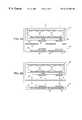
- the modulating layer 10 of FIG. 1 and the pixel layer 22 of FIG. 2, prepared separatelyare now integrated as illustrated in FIG. 3 to form a subassembly 30 .
- the pixel electrodes 24are brought in contact with a second surface 11 of the modulating layer 10 such that the common electrode 12 is provided next to the first surface 13 of the display media 14 and the pixel electrodes 24 are provided next to the second surface 11 of the display media 14 .
- the pixel layer 22can be joined with the modulating layer 10 by providing an adhesive material between the pixel layer 22 and the modulating layer 10 .
- the adhesive materialhas electrical, mechanical, and chemical properties that are compatible with those of the pixel layer 22 and the modulating layer 10 .
- the subassembly 30may be pressed together using standard pressing equipment well known to those skilled in the art, such as vacuum laminators and thermal presses.
- the edges of the subassembly 30can be sealed using a seal 32 as shown in FIG. 3 .
- the material for the edge seal 32can be selected from a number of commercially available materials, such as one or two-part epoxies.
- the subassembly 30is encapsulated in a protective material.
- the material for the encapsulantcan be selected from a number of commercially available transparent materials, such as vapor-deposited parylene.
- the contact pads 26remain exposed to provide electrical connection with a circuit layer.
- encapsulation with a protective materialcan take place after a final assembly of an electronic display is provided.
- the protective material used for encapsulationprotects the electro-optic material and the electronic elements from the environment.
- the subassembly 30is integrated with the circuit layer 40 .
- the circuit layer 40includes a substrate 41 , pixel electrode contacts 42 provided on a first surface 45 of the substrate 41 and pixel circuitry and logic 44 provided on the substrate 41 . Details of the circuit layer 40 will be discussed in reference to FIGS. 10 and 11.
- the subassembly 30is bonded to the circuit layer 40 using bonding techniques known to those skilled in the art, such as thermocompression, thermosonic bonding or mechanical bonding.
- an adhesive layer 46is provided between the second surface 25 of the pixel layer 22 of the subassembly 30 and a first surface 45 of the circuit layer 40 .
- the adhesive layer 46can be provided on the second surface 25 of the pixel layer 22 around the contact pads 26 and the first surface 45 of the circuit layer 30 around the pixel electrode contacts 42 .
- the adhesive layer 46can be made of a film coated on both sides with an adhesive material. Examples of such adhesive layers include Double Coated Film Tape Nos. 9443, 443, and 444 available from 3M Company (St. Paul, Minn.).
- the adhesive layer 46is printed on the second surface 25 of the pixel layer 22 and/or the first surface 45 of the circuit layer 40 .
- an anisotropic conductive film 47is provided between the second surface 25 of the pixel layer 22 and the first surface 45 of the circuit layer 40 .
- An anisotropic conductive film 47is conductive through one axis, such as the z-axis only.
- the anisotropic conductive film 47can consist of silver particles dispersed in an adhesive matrix such as Z-axis Adhesive Film Nos. 5303 and 7303 available from 3M Company (St. Paul, Minn.).
- the anisotropic conductive film 47can provide the electrical feed through between the contact pads 26 and the pixel electrode contacts 42 .
- a pressureis applied to the subassembly 30 and the circuit layer 40 to bond them together.
- Standard equipment known to those skilled in the artsuch as vacuum laminators and thermal presses, can be used for assembling the subassembly 30 and the circuit layer 40 to form the assembly 50 , as shown in FIG. 5 .
- the pixel layer 22 and the circuit layer 40are connected through edge connectors in addition to the vias 28 .
- the circuit layer 40 of the assembly 50can be further connected to a second circuit layer 70 .
- the second circuit layer 70can include additional electronics for driving the electronic display.
- the second circuit layer 70can include a flexible printed circuit board 72 and high performance integrated circuits 74 that perform control functions for the electronic display.
- the first circuit layer 40 and the second circuit layer 70can be connected through a ribbon cable 78 .
- the second circuit layer 70can be used in addressing the display media 14 .
- the second circuit layer 70can be used in addressing a second display media provided next to the second circuit layer 70 .
- an electronic displayincludes two display surfaces.
- the order of assembling the modulating layer 10 , the pixel layer 22 and the circuit layer 40is not limited to the order described in reference to FIGS. 1-3, 4 a- 4 b, and 5 .
- the pixel layer 22can be first laminated to the circuit layer 40 , forming a subassembly 35 , and subsequently the modulating layer 10 can be laminated to the subassembly 35 .
- This order of assembling the modulating layer 10 , the pixel layer 22 and the circuit layer 40is desirable where the bonding pressure and temperature required to laminate the pixel layer 22 to the circuit layer 40 is outside the processing regime of the modulating layer 10 .
- the alignment of the modulating layer 10 , the pixel layer 22 and the circuit layer 40can be facilitated by mechanical and/or photographic alignment markers.
- the alignment markerscan be printed on the second surface 25 of the pixel layer 22 and the first surface 45 of the circuit layer 40 in precise locations, preferably at opposite corners on the pixel layers 22 and the circuit layer 40 , and the relative positions of the pixel layer 22 and the circuit layer 44 layers can be adjusted until all markers are aligned.
- an alignment featurecan be embossed on one substrate and punched through the other substrate to provide an interlocking alignment joint.
- the method of assembling the electronic display according to the present inventionallows each of the modulating layer, the pixel layer and the circuit layer to be processed individually to optimize its performance characteristics.
- each of the modulating layer, the pixel layer, and the circuit layercan be tested after processing prior to assembly. Such capability reduces cost of production.
- a subassembly of the modulating layer and the pixel layercan be tested by simply contacting the subassembly with the circuit layer, prior to assembly.
- the display media used in forming the electronic displaycomprises a particle-based display media.
- the particle-based display mediacomprises an electronic ink.
- An electronic inkis an optoelectronically active material which comprises at least two phases: an electrophoretic contrast media phase and a coating/binding phase.
- the electrophoretic phasecomprises, in some embodiments, a single species of electrophoretic particles dispersed in a clear or dyed medium, or more than one species of electrophoretic particles having distinct physical and electrical characteristics dispersed in a clear or dyed medium.
- the electrophoretic phaseis encapsulated, that is, there is a capsule wall phase between the two phases.
- the coating/binding phaseincludes, in one embodiment, a polymer matrix that surrounds the electrophoretic phase.
- the polymer in the polymeric binderis capable of being dried, crosslinked, or otherwise cured as in traditional inks, and therefore a printing process can be used to deposit the electronic ink onto a substrate.
- the optical quality of an electronic inkis quite distinct from other electronic display materials.
- the most notable differenceis that the electronic ink provides a high degree of both reflectance and contrast because it is pigment based (as are ordinary printing inks).
- the light scattered from the electronic inkcomes from a very thin layer of pigment close to the top of the viewing surface. In this respect it resembles an ordinary, printed image.
- electronic inkis easily viewed from a wide range of viewing angles in the same manner as a printed page, and such ink approximates a Lambertian contrast curve more closely than any other electronic display material. Since electronic ink can be printed, it can be included on the same surface with any other printed material, including traditional inks.
- Electronic inkcan be made optically stable in all display configurations, that is, the ink can be set to a persistent optical state. Fabrication of a display by printing an electronic ink is particularly useful in low power applications because of this stability.
- Electronic ink displaysare novel in that they can be addressed by DC voltages and draw very little current.
- the conductive leads and electrodes used to deliver the voltage to electronic ink displayscan be of relatively high resistivity.
- the ability to use resistive conductorssubstantially widens the number and type of materials that can be used as conductors in electronic ink displays.
- ITOindium tin oxide
- the use of costly vacuum-sputtered indium tin oxide (ITO) conductorsa standard material in liquid crystal devices, is not required.
- the replacement of ITO with other materialscan provide benefits in appearance, processing capabilities (printed conductors), flexibility, and durability.
- the printed electrodesare in contact only with a solid binder, not with a fluid layer (like liquid crystals).
- conductive materialswhich would otherwise dissolve or be degraded by contact with liquid crystals, can be used in an electronic ink application.
- These conductive coatingsinclude conducting or semiconducting colloids, examples of which are indium tin oxide and antimony-doped tin oxide.
- Organic conductorspolymeric conductors and molecular organic conductors also may be used.
- Polymersinclude, but are not limited to, polyaniline and derivatives, polythiophene and derivatives, poly3,4-ethylenedioxythiophene (PEDOT) and derivatives, polypyrrole and derivatives, and polyphenylenevinylene (PPV) and derivatives.
- Organic molecular conductorsinclude, but are not limited to, derivatives of naphthalene, phthalocyanine, and pentacene.
- Polymer layerscan be made thinner and more transparent than with traditional displays because conductivity requirements are not as stringent.
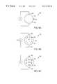
- FIG. 8 ashows an electrophoretic display 130 .
- the binder 132includes at least one capsule 134 , which is filled with a plurality of particles 136 and a dyed suspending fluid 138 .
- the particles 136are titania particles.
- a direct-current electric field of the appropriate polarityis applied across the capsule 134 , the particles 136 move to the viewed surface of the display and scatter light.
- the applied electric fieldis reversed, the particles 136 move to the rear surface of the display and the viewed surface of the display then appears dark.
- FIG. 8 bshows another electrophoretic display 140 .
- This displaycomprises a first set of particles 142 and a second set of particles 144 in a capsule 141 .
- the first set of particles 142 and the second set of particles 144have contrasting optical properties.
- the first set of particles 142 and the second set of particles 144can have differing electrophoretic mobilities.
- the first set of particles 142 and the second set of particles 144can have contrasting colors.
- the first set of particles 142can be white, while the second set of particles 144 can be black.
- the capsule 141further includes a substantially clear fluid.
- the capsule 141has electrodes 146 and 146 ′ disposed adjacent it.
- the electrodes 146 , 146 ′are connected to a source of voltage 148 , which may provide an alternating-current (AC) field or a direct-current (DC) field to the capsule 441 .
- a source of voltage 148may provide an alternating-current (AC) field or a direct-current (DC) field to the capsule 441 .
- ACalternating-current
- DCdirect-current
- FIG. 8 cshows a suspended particle display 150 .
- the suspended particle display 150includes needle-like particles 152 in a transparent fluid 154 .
- the particles 152change their orientation upon application of an AC field across the electrodes 156 , 156 ′. When the AC field is applied, the particles 152 are oriented perpendicular with respect to the display surface and the display appears transparent. When the AC field is removed, the particles 152 are randomly oriented and the display 150 appears opaque.
- FIGS. 8 a- 8 care exemplary only, and other electrophoretic displays can be used in accordance with the present invention.
- Other examples of electrophoretic displaysare described in commonly owned, copending U.S. patent application Ser. Nos. 08/935,800 and 09/140,792 which are incorporated herein by reference.
- an encapsulated electrophoretic displayrequires the proper interaction of a binder for binding the capsules to a substrate, electrophoretic particles, fluid (for example, to surround the electrophoretic particles and provide a medium for migration), and a capsule membrane (for example, for enclosing the electrophoretic particles and fluid). These components must all be chemically compatible.
- the capsule membranesmay engage in useful surface interactions with the electrophoretic particles, or may act as an inert physical boundary between the fluid and the binder.
- Polymer bindersmay set as adhesives between capsule membranes and electrode surfaces.
- Various materialsmay be used to create electrophoretic displays. Selection of these materials is based on the functional constituents of the display to be manufactured. Such functional constituents include, but are not limited to, particles, dyes, suspending fluids, stabilizing/charging additives, and binders.
- types of particles that may be used to fabricate suspended particle displaysinclude scattering pigments, absorbing pigments and luminescent particles. Such particles may also be transparent.
- Exemplary particlesinclude titania, which may be coated in one or two layers with a metal oxide, such as aluminum oxide or silicon oxide, for example. Such particles may be constructed as corner cubes.
- Luminescent particlesmay include, for example, zinc sulfide particles.
- the zinc sulfide particlesmay also be encapsulated with an insulative coating to reduce electrical conduction.
- Light-blocking or absorbing particlesmay include, for example, dyes or pigments. Types of dyes for use in electrophoretic displays are commonly known in the art. Useful dyes are typically soluble in the suspending fluid, and may further be part of a polymeric chain. Dyes may be polymerized by thermal, photochemical, and chemical diffusion processes. Single dyes or mixtures of dyes may also be used.
- a suspending (i.e., electrophoretic) fluidmay be a high resistivity fluid.
- the suspending fluidmay be a single fluid, or it may be a mixture of two or more fluids.
- the suspending fluidwhether a single fluid or a mixture of fluids, may have its density substantially matched to that of the particles within the capsule.
- the suspending fluidmay be halogenated hydrocarbon, such as tetrachloroethylene, for example.
- the halogenated hydrocarbonmay also be a low molecular weight polymer.
- One such low molecular weight polymeris poly(chlorotrifluoroethylene). The degree of polymerization for this polymer may be from about 2 to about 10.
- capsulesmay be formed in, or later dispersed in, a binder.
- Materials for use as bindersinclude water-soluble polymers, water-dispersed polymers, oil-soluble polymers, thermoset polymers, thermoplastic polymers, and UV- or radiation-cured polymers.
- the electrophoretic fluidmay be directly dispersed or emulsified into the binder (or a precursor to the binder material) to form what may be called a “polymer-dispersed electrophoretic display.”
- the individual electrophoretic phasesmay be referred to as capsules or microcapsules even though no capsule membrane is present.
- Such polymer-dispersed electrophoretic displaysare considered to be subsets of encapsulated electrophoretic displays.
- the binder materialsurrounds the capsules and separates the two bounding electrodes.
- This binder materialmust be compatible with the capsule and bounding electrodes and must possess properties that allow for facile printing or coating. It may also possess barrier properties for water, oxygen, ultraviolet light, the electrophoretic fluid, or other materials. Further, it may contain surfactants and cross-linking agents, which could aid in coating or durability.
- the polymer-dispersed electrophoretic displaymay be of the emulsion or phase separation type.
- the display mediacan comprise a plurality of bichromal spheres shown in FIG. 8 d.
- a bichromal sphere 160typically comprises a positively charged hemisphere 162 of a first color and a negatively charged hemisphere 164 of a second color in a liquid medium 166 .
- the sphere 160rotates and displays the color of one of the two hemispheres 162 , 164 .
- an electronic displayis created by printing the entire display or a portion of the display.
- printingis intended to include all forms of printing and coating, including: inkjet printing, premetered coating such as patch die coating, slot or extrusion coating, slide or cascade coating, and curtain coating; roll coating such as knife over roll coating, forward and reverse roll coating; gravure coating; dip coating; spray coating; meniscus coating; spin coating; brush coating; air knife coating; screen printing processes; electrostatic printing processes; thermal printing processes; and other similar techniques.
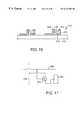
- the pixel layer 200includes a substrate 202 having a first surface 204 and a second surface 206 .
- the substrate 202can be made of an insulating polymeric material such as polyethylene terephthalate (PET, polyester), polyethersulphone (PES), polyimid film (e.g. Kapton, available from Dupont [Wilington, Del.]; Upilex, available from Ube Corporation [Japan]), or polycarbonate.
- PETpolyethylene terephthalate
- PESpolyethersulphone
- polyimid filme.g. Kapton, available from Dupont [Wilington, Del.]; Upilex, available from Ube Corporation [Japan]
- An advantage of the insulator substrate 202is that the substrate 202 protects the display media, as well as the pixel electrodes 208 from the environment.
- An array of pixel electrodes 208are provided on the first surface 204 of the substrate 202 .
- the pixel electrodes 208are arranged in a manner to obtain high aperture ratio or fill factor.
- An electrically conductive materialcan be evaporated or printed on the first surface 204 of the substrate 202 to form the pixel electrodes 208 .
- the pixel electrodes 208are connected to the second surface 206 of the substrate 202 through electrical vias 210 .
- the electrical vias 210can be formed using one of several techniques. For example, holes can be made in the pixel layer 200 by either laser drilling, etching or pricking the holes. The holes are then filled by printing a low resistivity slurry such as carbon, graphite, or silver particles in a polymeric compound.
- An array of contact pads 212are provided on the second surface 206 of the pixel layer 200 .
- the contact pads 212can be made using one of many available methods known to those skilled in the art.
- a conductive materialcan be evaporated or printed on the second surface 206 of the substrate 202 to form the contact pads 212 .
- the pixel layercan be further processed to include various electrical, thermal and optical layers to improve display performance.
- thermoelectric (TE) heaters or coolerscan be provided on either surface of the substrate 202 , as permitted by space availability, to ensure that the electro-optical material stays within its thermal operating regime.
- Thermoelectric heatersmay be integrated by providing traces of resistive material on a surface of the substrate 202 . By passing an electrical current through these traces, the display temperature can be regulated.
- thermoelectric coolerssuch as a Peltier cooler, can be used to move thermal energy from the display to a suitable heat sink.
- the pixel layercan also include grounded thin metal foils and/or reflective or opaque light shields. Grounded thin-metal foils or light shields can be used to enhance the optical performance of the display and optically shield photosensitive microelectronics from light.
- the pixel layer or the circuit layermay incorporate semiconducting materials, many of which are known to be photosensitive. Thin foils or light shields may be incorporated onto one or more surfaces of the pixel layer or the circuit layer so that the photosensitive materials are optically shielded from all incident light.
- the circuit layercan include electrodes such as column electrodes and row electrodes, non-linear devices, and logic or driver circuitry for addressing the display.
- the circuit layercan include transistors shown in FIGS. 10 and 11.
- an organic-based field effect transistor 210includes a substrate 212 , a gate electrode 214 provided on the substrate 212 , a dielectric layer 216 provided on the gate electrode 214 , an organic semiconductor 218 provided on the dielectric layer 216 , and a source electrode 220 and a drain electrode 222 provided on the organic semiconductor 218 .
- the transistor 210is electrically connected to a pixel electrode 200 , a column electrode 204 and a row electrode 206 .
- the pixel electrode 200is connected to the drain electrode of the transistor 210 .
- the column electrode 204is connected to the source electrode of the transistor 210 .
- the substrate 212can be flexible.
- the substrate 212can be made of a polymer, such as polyethylene terephthalate (PET, polyester), polyethersulphone (PES), polyimide film (Kapton, Upilex), or polycarbonate.
- PETpolyethylene terephthalate
- PESpolyethersulphone
- the substrate 212can be made of an insulator such as undoped silicon, glass, or other plastic.
- the substrate 212can also be patterned to serve as an electrode.
- the substrate 212can be a metal foil insulated from the gate electrode 214 by a non-conducting material.
- the gate electrode 214 , the source electrode 220 , and the drain electrode 222for example, can comprise a metal such as gold.
- the electrodes 214 , 220 , 222can comprise a conductive polymer such as polythiophene or polyaniline, a printed conductor such as a polymer film comprising metal particles such as silver or nickel, a printed conductor comprising a polymer film containing graphite or some other conductive carbon material, or a conductive oxide such as tin oxide or indium tin oxide, or metal electrodes such as aluminum or gold.
- a conductive polymersuch as polythiophene or polyaniline
- a printed conductorsuch as a polymer film comprising metal particles such as silver or nickel
- a printed conductorcomprising a polymer film containing graphite or some other conductive carbon material
- a conductive oxidesuch as tin oxide or indium tin oxide
- metal electrodessuch as aluminum or gold.
- the dielectric layer 216can comprise a silicon dioxide layer.
- the dielectric layer 216can comprise an insulating polymer such as polyimide and its derivatives or poly-vinyl phenol, polymethylmethacrylate, polyvinyldenedifluoride, an inorganic oxide such as metal oxide, an inorganic nitride such as silicon nitride, or an inorganic/organic composite material such as an organic-substituted silicon oxide, of a sol-gel organosilicon glass.
- the dielectric layer 216can also comprise a benzocyclobutene (BCB) derivative marketed by Dow Chemical (Midland, Mich.), spin-on glass, or dispersions of dielectric colloid materials in a binder or solvent.
- BCBbenzocyclobutene
- the semiconductor layer 218can be an organic polymer.
- the organic semiconductorcomprises a polymeric or oligomeric semiconductor.
- suitable polymeric semiconductorsinclude, but are not limited to, polythiophene, poly(3-alkyl), alkyl-substituted oligothiophene, polythienylenevinylene, poly(para-phenylenevinylene) and doped versions of these polymers.
- An example of suitable oligomeric semiconductoris alpha-hexathienylene. Horowitz, Organic Field-Effect Transistors, Adv. Mater., 10, No. 5, p. 365 (1998) describes the use of unsubstituted and alkyl-substituted oligothiophenes in transistors.
- a field effect transistor made with regioregular poly(3-hexylthiophene) as the semiconductor layeris described in Bao et al., Soluble and Processable Regioregular Poly (3- hexylthiophene ) for Thin Film Field - Effect Transistor Applications with High Mobility, Appl. Phys. Lett. 69 (26), p. 4108 (December 1996).
- a field effect transistor made with ⁇ -hexathienyleneis described in U.S. Pat. No. 5,659,181.
- the organic semiconductor 218comprises a carbon based compound.
- suitable carbon based compoundsinclude, but are not limited to, pentacene, phthalocyanine, benzodithiophene, fullerene, buckminsterfullerene, tetracyanonaphthoquinone, and tetrakisimethylanimoethylene.
- the materials provided above for forming the substrate, the dielectric layer, the electrodes, or the semiconductor layerare exemplary only. Other suitable materials known to those skilled in the art having properties similar to those described above can be used in accordance with the present invention.
- FIGS. 10 and 11are exemplary only. Other transistor designs known to those skilled in the art can be used in accordance with the present invention.
- a top gate structure in which the source and drain electrodes are placed adjacent the substrate, covered by the dielectric layer, which in turn is covered by the semiconductor and gate electrode,can also be used in accordance with the present invention.
- electrodes, non-linear devices such as the transistors of FIGS. 10 and 11, and logic and driving circuitrycan be manufactured using any appropriate fabrication process known to those skilled in the art including, but not limited to, deposition, evaporation, lithography, printing, and coating.
- an entire transistor that is organic-basedcan be printed in its entirety as described in co-pending commonly owned U.S. patent application Ser. No. 09/289,036, incorporated herein by reference.
- a transistorcan be fabricated on a first substrate and subsequently removed and provided on a substrate of the circuit layer as described in co-pending commonly owned U.S. patent application Ser. No. 09/338,412, incorporated herein by reference.
Landscapes
- Physics & Mathematics (AREA)
- Nonlinear Science (AREA)
- Optics & Photonics (AREA)
- General Physics & Mathematics (AREA)
- Chemical & Material Sciences (AREA)
- Crystallography & Structural Chemistry (AREA)
- Mathematical Physics (AREA)
- Electrochemistry (AREA)
- Molecular Biology (AREA)
- Health & Medical Sciences (AREA)
- Chemical Kinetics & Catalysis (AREA)
- Life Sciences & Earth Sciences (AREA)
- Engineering & Computer Science (AREA)
- Microelectronics & Electronic Packaging (AREA)
- Electrochromic Elements, Electrophoresis, Or Variable Reflection Or Absorption Elements (AREA)
- Liquid Crystal (AREA)
Abstract
Description
The present application claims priority to provisional application U.S. Ser. No. 60/112,330 filed on Dec. 15, 1998, the entire disclosure of which is incorporated herein by reference. The present application is a continuation-in-part of utility applications U.S. Ser. No. 09/338,412 filed on Jun. 22, 1999, now abandoned, and U.S. Ser. No. 09/289,036 filed on Apr. 9, 1999, the entire disclosures of which are incorporated herein by reference.
This invention generally relates to methods of manufacturing an electronic display, and more particularly, to methods of assembling electronic displays.
An electronic display includes optical components such as liquid crystals and electrophoretic particles and electronic components such as electrodes and driving circuitry. The optical components and the electronic components have differing performance criteria. For example, it is desirable for the optical components to optimize reflectivity, contrast ratio and response time, while it is desirable for the electronic components to optimize conductivity, voltage-current relationship, and capacitance, or to possess memory, logic, or other higher-order electronic device capabilities. Therefore, a process for manufacturing an optical component may not be ideal for manufacturing an electronic component, and vice versa. For example, a process for manufacturing an electronic component can involve processing under high temperatures. The processing temperature can be in the range from about 300° C. to about 600° C. Subjecting many optical components to such high temperatures, however, can be harmful to the optical components by degrading the elements (i.e., the electrophoretic particles or liquid crystals) chemically or by causing mechanical damage.
One way to circumvent this problem is to change the chronology of display fabrication, in which the electronic components requiring high temperature processing are processed first, and the optical components requiring low temperature processing are processed second. Another way to circumvent this problem is to process the optical components and the electrical components separately and then integrate the two components, afterwards.
The present invention relates to a method of manufacturing an electro-optical device. In one aspect, the electro-optical device is manufactured in accordance with the following steps. First, a modulating layer, a pixel layer, and a circuit layer are provided. The modulating layer includes a first substrate and an electro-optical material provided adjacent the first substrate. The modulating layer is capable of changing a visual state upon application of an electric field. The pixel layer comprises a second substrate. A plurality of pixel electrodes are provided on a front surface of the second substrate and a plurality of contact pads are provided on a rear surface of the second substrate. Each pixel electrode is connected to a contact pad through a via extending through the second substrate. The circuit layer includes a third substrate and at least one circuit element. The modulating layer, the pixel layer, and the circuit layer are integrated to form the electro-optical device.
In one embodiment, the pixel layer and the modulating layer are integrated first to form a subassembly, and thereafter, the circuit layer and the subassembly are integrated to form the electro-optical device. For example, the pixel layer and the modulating layer can be integrated through encapsulation. Alternatively, an edge of the pixel layer and an edge of the modulating layer can be sealed together. The circuit layer and the subassembly can be integrated by bonding the two layers. For example, the circuit layer and the subassembly can be bonded by inserting an adhesive layer comprising an anisotropically conductive material between the two layers.
In another embodiment, the pixel layer and the circuit layer are integrated first to form a subassembly and thereafter, the modulating layer and the subassembly are integrated to form the electro-optical device.
In one embodiment, the electro-optical material comprises a plurality of capsules, each capsule comprising a plurality of particles dispersed in a fluid. For example, the plurality of particles can be electrophoretic particles. In another embodiment, the electro-optical material comprises liquid crystals. In still another embodiment, the electro-optical material comprises a plurality of capsules, each capsule comprising a bichromal sphere dispersed in a fluid.
In one embodiment, the modulating layer comprises a flexible substrate. For example, the modulating layer can be an organic substrate.
In one embodiment, the pixel layer comprises an insulative substrate. The pixel layer can be formed by printing or evaporating a conductive material on the front surface of the substrate to form the pixel electrodes.
In one embodiment, the circuit layer includes one or more of the following elements: a data line driver, a select line driver, a power supply, a sensor, a logic element, a memory device and a communication device. For example, the circuit layer can include non-linear devices such as transistors. The transistors can be made by printing organic-based field effect transistors on a front surface of the circuit layer.
In one embodiment, the modulating layer, the pixel layer, and the circuit layer are tested prior to being integrated.
In another aspect, the invention features an electro-optical device manufactured using the methods described herein. The electro-optical device can be an electronic display.
The foregoing and other objects, features and advantages of the present invention, as well as the invention itself, will be more fully understood from the following description of preferred embodiments, when read together with the accompanying drawings, in which:
FIG. 1 shows a cross-section view of a modulating layer of an electronic display, according to one embodiment of the present invention.
FIG. 2 shows a cross-section view of a pixel layer of an electronic display, according to one embodiment of the present invention.
FIG. 3 shows a cross-section view of a subassembly of the modulating layer of FIG.1 and the pixel layer of FIG. 2, according to one embodiment of the present invention.
FIG. 4aillustrates integration of the subassembly of FIG. 3 and a circuit layer, according to one embodiment of the present invention.
FIG. 4billustrates integration of the subassembly of FIG. 3 and a circuit layer, according to another embodiment of the present invention.
FIG. 5 shows a cross-section of an electronic ink assembly, according to one embodiment of the present invention.
FIG. 6aillustrates integration of the electronic ink assembly of FIG. 5 and a second circuit layer, according to one embodiment of the present invention.
FIG. 6bshows a cross-section of an electronic ink integrated using the method illustrated in FIG. 6a.
FIG. 7aillustrates integration of a pixel layer and a circuit layer to form a subassembly, according to one embodiment of the present invention.
FIG. 7billustrates integration of a subassembly of a pixel layer and a circuit layer to a modulator layer, according to one embodiment of the present invention.
FIG. 8ashows a partial cross-section view of an electronic display media, according to one embodiment of the present invention.
FIG. 8bshows a partial cross-section view of an electronic display media, according to one embodiment of the present invention.
FIG. 8cshows a partial cross-section view of an electronic display media, according to one embodiment of the present invention.
FIG. 8dshows a partial cross-section view of an electronic display media, according to one embodiment of the present invention.
FIG. 9ashows a first surface of a pixel layer, according to one embodiment of the present invention.
FIG. 9bshows a second surface of a pixel layer, according to one embodiment of the present invention.
FIG. 10 shows a partial cross-section view of transistors for addressing an electronic display, according to one embodiment of the present invention.
FIG. 11 illustrates a connection between a transistor and electrodes of an electronic display, according to one embodiment of the present invention.
The present invention relates to a method of assembling or packing an electronic display. Referring to FIG. 1, amodulating layer 10 prepared using methods to be described, which optimize the optical qualities of themodulating layer 10, is provided. The modulatinglayer 10 includes asubstrate 12 and adisplay media 14 provided next to thesubstrate 12. Thesubstrate 12 includes a frontcommon electrode 16 deposited on afirst surface 13 of thesubstrate 12 next to thedisplay media 14. Thedisplay media 14 includesmicrocapsules 18 dispersed in abinder 20. Eachmicrocapsule 18 includes an electro-optical material. An electro-optical material refers to a material which displays an optical property in response to an electrical signal. Examples of electro-optical material can be electrophoretic particles or a liquid crystalline fluid dispersed in a solvent. An electro-optical material can also be bichromal spheres dispersed in a solvent. Details of electro-optical materials within themicrocapsules 18 will be discussed further in reference to FIGS. 8a-8d.An important property of the electro-optical material within themicrocapsules 18 is that the material is capable of displaying one visual state upon application of an electric field and a different visual state upon application of a different electric field.
Referring to FIG. 2, apixel layer 22, prepared using methods to be discussed which optimize the electrical properties of thepixel layer 22, is provided. Thepixel layer 22 includes asubstrate 23,pixel electrodes 24 provided on afirst surface 21 of thesubstrate 23, andcontact pads 26 provided on asecond surface 25 of thesubstrate 23. Eachpixel electrode 24 is electrically connected to acontact pad 26 through a via28. In order to maximize probability of electrical contact between thepixel electrode 24 and thecontact pad 26, more than one via28 can be provided between eachpixel electrode 24 and itscorresponding contact pad 26, as illustrated in FIG.2. Thepixel layer 22 will be discussed in detail with reference to FIGS. 9aand9b.
The modulatinglayer 10 of FIG.1 and thepixel layer 22 of FIG. 2, prepared separately are now integrated as illustrated in FIG. 3 to form asubassembly 30. Thepixel electrodes 24 are brought in contact with asecond surface 11 of themodulating layer 10 such that thecommon electrode 12 is provided next to thefirst surface 13 of thedisplay media 14 and thepixel electrodes 24 are provided next to thesecond surface 11 of thedisplay media 14. Thepixel layer 22 can be joined with themodulating layer 10 by providing an adhesive material between thepixel layer 22 and themodulating layer 10. The adhesive material has electrical, mechanical, and chemical properties that are compatible with those of thepixel layer 22 and themodulating layer 10. To ensure intimate connection between thepixel layer 22 and themodulating layer 10, thesubassembly 30 may be pressed together using standard pressing equipment well known to those skilled in the art, such as vacuum laminators and thermal presses.
The edges of thesubassembly 30 can be sealed using aseal 32 as shown in FIG.3. The material for theedge seal 32 can be selected from a number of commercially available materials, such as one or two-part epoxies. In another embodiment, thesubassembly 30 is encapsulated in a protective material. The material for the encapsulant can be selected from a number of commercially available transparent materials, such as vapor-deposited parylene. In this embodiment, thecontact pads 26 remain exposed to provide electrical connection with a circuit layer. Alternatively, encapsulation with a protective material can take place after a final assembly of an electronic display is provided. The protective material used for encapsulation protects the electro-optic material and the electronic elements from the environment.
Referring to FIGS. 4aand4b,thesubassembly 30 is integrated with thecircuit layer 40. Thecircuit layer 40 includes asubstrate 41,pixel electrode contacts 42 provided on afirst surface 45 of thesubstrate 41 and pixel circuitry andlogic 44 provided on thesubstrate 41. Details of thecircuit layer 40 will be discussed in reference to FIGS. 10 and 11. In one embodiment, thesubassembly 30 is bonded to thecircuit layer 40 using bonding techniques known to those skilled in the art, such as thermocompression, thermosonic bonding or mechanical bonding.
In the embodiment of FIG. 4a,anadhesive layer 46 is provided between thesecond surface 25 of thepixel layer 22 of thesubassembly 30 and afirst surface 45 of thecircuit layer 40. To improve adhesion and planarization, theadhesive layer 46 can be provided on thesecond surface 25 of thepixel layer 22 around thecontact pads 26 and thefirst surface 45 of thecircuit layer 30 around thepixel electrode contacts 42. Theadhesive layer 46, for example, can be made of a film coated on both sides with an adhesive material. Examples of such adhesive layers include Double Coated Film Tape Nos. 9443, 443, and 444 available from 3M Company (St. Paul, Minn.). In one embodiment, theadhesive layer 46 is printed on thesecond surface 25 of thepixel layer 22 and/or thefirst surface 45 of thecircuit layer 40.
In the embodiment of FIG. 4b,an anisotropicconductive film 47 is provided between thesecond surface 25 of thepixel layer 22 and thefirst surface 45 of thecircuit layer 40. An anisotropicconductive film 47 is conductive through one axis, such as the z-axis only. The anisotropicconductive film 47 can consist of silver particles dispersed in an adhesive matrix such as Z-axis Adhesive Film Nos. 5303 and 7303 available from 3M Company (St. Paul, Minn.). The anisotropicconductive film 47 can provide the electrical feed through between thecontact pads 26 and thepixel electrode contacts 42.
After providing theadhesive layer pixel layer 22 and thecircuit layer 30, a pressure is applied to thesubassembly 30 and thecircuit layer 40 to bond them together. Standard equipment known to those skilled in the art, such as vacuum laminators and thermal presses, can be used for assembling thesubassembly 30 and thecircuit layer 40 to form theassembly 50, as shown in FIG.5. In one embodiment, thepixel layer 22 and thecircuit layer 40 are connected through edge connectors in addition to thevias 28.
Referring to FIGS. 6aand6b,thecircuit layer 40 of theassembly 50 can be further connected to asecond circuit layer 70. Thesecond circuit layer 70 can include additional electronics for driving the electronic display. Thesecond circuit layer 70 can include a flexible printedcircuit board 72 and high performanceintegrated circuits 74 that perform control functions for the electronic display. Thefirst circuit layer 40 and thesecond circuit layer 70 can be connected through aribbon cable 78. Thesecond circuit layer 70 can be used in addressing thedisplay media 14. Alternatively, thesecond circuit layer 70 can be used in addressing a second display media provided next to thesecond circuit layer 70. In this embodiment, an electronic display includes two display surfaces.
The order of assembling themodulating layer 10, thepixel layer 22 and thecircuit layer 40 is not limited to the order described in reference to FIGS. 1-3,4a-4b,and5. Referring to FIGS. 7aand7b,thepixel layer 22 can be first laminated to thecircuit layer 40, forming asubassembly 35, and subsequently themodulating layer 10 can be laminated to thesubassembly 35. This order of assembling themodulating layer 10, thepixel layer 22 and thecircuit layer 40 is desirable where the bonding pressure and temperature required to laminate thepixel layer 22 to thecircuit layer 40 is outside the processing regime of themodulating layer 10.
The alignment of themodulating layer 10, thepixel layer 22 and thecircuit layer 40 can be facilitated by mechanical and/or photographic alignment markers. For example, the alignment markers can be printed on thesecond surface 25 of thepixel layer 22 and thefirst surface 45 of thecircuit layer 40 in precise locations, preferably at opposite corners on the pixel layers22 and thecircuit layer 40, and the relative positions of thepixel layer 22 and thecircuit layer 44 layers can be adjusted until all markers are aligned. For a plastic or deformable substrate, an alignment feature can be embossed on one substrate and punched through the other substrate to provide an interlocking alignment joint.
The method of assembling the electronic display according to the present invention, allows each of the modulating layer, the pixel layer and the circuit layer to be processed individually to optimize its performance characteristics. In addition, each of the modulating layer, the pixel layer, and the circuit layer can be tested after processing prior to assembly. Such capability reduces cost of production. In one embodiment, a subassembly of the modulating layer and the pixel layer can be tested by simply contacting the subassembly with the circuit layer, prior to assembly.
In one embodiment, the display media used in forming the electronic display comprises a particle-based display media. In one detailed embodiment, the particle-based display media comprises an electronic ink. An electronic ink is an optoelectronically active material which comprises at least two phases: an electrophoretic contrast media phase and a coating/binding phase. The electrophoretic phase comprises, in some embodiments, a single species of electrophoretic particles dispersed in a clear or dyed medium, or more than one species of electrophoretic particles having distinct physical and electrical characteristics dispersed in a clear or dyed medium. In some embodiments the electrophoretic phase is encapsulated, that is, there is a capsule wall phase between the two phases. The coating/binding phase includes, in one embodiment, a polymer matrix that surrounds the electrophoretic phase. In this embodiment, the polymer in the polymeric binder is capable of being dried, crosslinked, or otherwise cured as in traditional inks, and therefore a printing process can be used to deposit the electronic ink onto a substrate.
The optical quality of an electronic ink is quite distinct from other electronic display materials. The most notable difference is that the electronic ink provides a high degree of both reflectance and contrast because it is pigment based (as are ordinary printing inks). The light scattered from the electronic ink comes from a very thin layer of pigment close to the top of the viewing surface. In this respect it resembles an ordinary, printed image. Also, electronic ink is easily viewed from a wide range of viewing angles in the same manner as a printed page, and such ink approximates a Lambertian contrast curve more closely than any other electronic display material. Since electronic ink can be printed, it can be included on the same surface with any other printed material, including traditional inks. Electronic ink can be made optically stable in all display configurations, that is, the ink can be set to a persistent optical state. Fabrication of a display by printing an electronic ink is particularly useful in low power applications because of this stability.
Electronic ink displays are novel in that they can be addressed by DC voltages and draw very little current. As such, the conductive leads and electrodes used to deliver the voltage to electronic ink displays can be of relatively high resistivity. The ability to use resistive conductors substantially widens the number and type of materials that can be used as conductors in electronic ink displays. In particular, the use of costly vacuum-sputtered indium tin oxide (ITO) conductors, a standard material in liquid crystal devices, is not required. Aside from cost savings, the replacement of ITO with other materials can provide benefits in appearance, processing capabilities (printed conductors), flexibility, and durability. Additionally, the printed electrodes are in contact only with a solid binder, not with a fluid layer (like liquid crystals). This means that some conductive materials, which would otherwise dissolve or be degraded by contact with liquid crystals, can be used in an electronic ink application. These include opaque metallic inks for the rear electrode (e.g., silver and graphite inks), as well as conductive transparent inks for either substrate. These conductive coatings include conducting or semiconducting colloids, examples of which are indium tin oxide and antimony-doped tin oxide. Organic conductors (polymeric conductors and molecular organic conductors) also may be used. Polymers include, but are not limited to, polyaniline and derivatives, polythiophene and derivatives, poly3,4-ethylenedioxythiophene (PEDOT) and derivatives, polypyrrole and derivatives, and polyphenylenevinylene (PPV) and derivatives. Organic molecular conductors include, but are not limited to, derivatives of naphthalene, phthalocyanine, and pentacene. Polymer layers can be made thinner and more transparent than with traditional displays because conductivity requirements are not as stringent.
FIG. 8ashows anelectrophoretic display 130. Thebinder 132 includes at least onecapsule 134, which is filled with a plurality ofparticles 136 and a dyed suspendingfluid 138. In one embodiment, theparticles 136 are titania particles. When a direct-current electric field of the appropriate polarity is applied across thecapsule 134, theparticles 136 move to the viewed surface of the display and scatter light. When the applied electric field is reversed, theparticles 136 move to the rear surface of the display and the viewed surface of the display then appears dark.
FIG. 8bshows anotherelectrophoretic display 140. This display comprises a first set ofparticles 142 and a second set ofparticles 144 in acapsule 141. The first set ofparticles 142 and the second set ofparticles 144 have contrasting optical properties. For example, the first set ofparticles 142 and the second set ofparticles 144 can have differing electrophoretic mobilities. In addition, the first set ofparticles 142 and the second set ofparticles 144 can have contrasting colors. For example, the first set ofparticles 142 can be white, while the second set ofparticles 144 can be black. Thecapsule 141 further includes a substantially clear fluid. Thecapsule 141 haselectrodes electrodes capsule 441. Upon application of an electric field across theelectrodes particles 142 move towardelectrode 146′, while the second set ofparticles 144 move towardelectrode 146.
FIG. 8cshows a suspendedparticle display 150. The suspendedparticle display 150 includes needle-like particles 152 in atransparent fluid 154. Theparticles 152 change their orientation upon application of an AC field across theelectrodes particles 152 are oriented perpendicular with respect to the display surface and the display appears transparent. When the AC field is removed, theparticles 152 are randomly oriented and thedisplay 150 appears opaque.
The electrophoretic displays provided in FIGS. 8a-8care exemplary only, and other electrophoretic displays can be used in accordance with the present invention. Other examples of electrophoretic displays are described in commonly owned, copending U.S. patent application Ser. Nos. 08/935,800 and 09/140,792 which are incorporated herein by reference.
The successful construction of an encapsulated electrophoretic display requires the proper interaction of a binder for binding the capsules to a substrate, electrophoretic particles, fluid (for example, to surround the electrophoretic particles and provide a medium for migration), and a capsule membrane (for example, for enclosing the electrophoretic particles and fluid). These components must all be chemically compatible. The capsule membranes may engage in useful surface interactions with the electrophoretic particles, or may act as an inert physical boundary between the fluid and the binder. Polymer binders may set as adhesives between capsule membranes and electrode surfaces.
Various materials may be used to create electrophoretic displays. Selection of these materials is based on the functional constituents of the display to be manufactured. Such functional constituents include, but are not limited to, particles, dyes, suspending fluids, stabilizing/charging additives, and binders. In one embodiment, types of particles that may be used to fabricate suspended particle displays include scattering pigments, absorbing pigments and luminescent particles. Such particles may also be transparent. Exemplary particles include titania, which may be coated in one or two layers with a metal oxide, such as aluminum oxide or silicon oxide, for example. Such particles may be constructed as corner cubes. Luminescent particles may include, for example, zinc sulfide particles. The zinc sulfide particles may also be encapsulated with an insulative coating to reduce electrical conduction. Light-blocking or absorbing particles may include, for example, dyes or pigments. Types of dyes for use in electrophoretic displays are commonly known in the art. Useful dyes are typically soluble in the suspending fluid, and may further be part of a polymeric chain. Dyes may be polymerized by thermal, photochemical, and chemical diffusion processes. Single dyes or mixtures of dyes may also be used.
A suspending (i.e., electrophoretic) fluid may be a high resistivity fluid. The suspending fluid may be a single fluid, or it may be a mixture of two or more fluids. The suspending fluid, whether a single fluid or a mixture of fluids, may have its density substantially matched to that of the particles within the capsule. The suspending fluid may be halogenated hydrocarbon, such as tetrachloroethylene, for example. The halogenated hydrocarbon may also be a low molecular weight polymer. One such low molecular weight polymer is poly(chlorotrifluoroethylene). The degree of polymerization for this polymer may be from about 2 to about 10.
Furthermore, capsules may be formed in, or later dispersed in, a binder. Materials for use as binders include water-soluble polymers, water-dispersed polymers, oil-soluble polymers, thermoset polymers, thermoplastic polymers, and UV- or radiation-cured polymers.
While the examples described here are listed using encapsulated electrophoretic displays, there are other particle-based display media that also should work well, including encapsulated suspended particles and rotating ball displays. Other display media, such as liquid crystals and magnetic particles, also can be useful.
In some cases, a separate encapsulation step of the process is not necessary. The electrophoretic fluid may be directly dispersed or emulsified into the binder (or a precursor to the binder material) to form what may be called a “polymer-dispersed electrophoretic display.” In such displays, the individual electrophoretic phases may be referred to as capsules or microcapsules even though no capsule membrane is present. Such polymer-dispersed electrophoretic displays are considered to be subsets of encapsulated electrophoretic displays.
In an encapsulated electrophoretic display, the binder material surrounds the capsules and separates the two bounding electrodes. This binder material must be compatible with the capsule and bounding electrodes and must possess properties that allow for facile printing or coating. It may also possess barrier properties for water, oxygen, ultraviolet light, the electrophoretic fluid, or other materials. Further, it may contain surfactants and cross-linking agents, which could aid in coating or durability. The polymer-dispersed electrophoretic display may be of the emulsion or phase separation type.
In another detailed embodiment, the display media can comprise a plurality of bichromal spheres shown in FIG. 8d.Abichromal sphere 160 typically comprises a positively chargedhemisphere 162 of a first color and a negatively chargedhemisphere 164 of a second color in aliquid medium 166. Upon application of an electric field across thesphere 160 through a pair ofelectrodes sphere 160 rotates and displays the color of one of the twohemispheres
In one embodiment, an electronic display is created by printing the entire display or a portion of the display. The term “printing” is intended to include all forms of printing and coating, including: inkjet printing, premetered coating such as patch die coating, slot or extrusion coating, slide or cascade coating, and curtain coating; roll coating such as knife over roll coating, forward and reverse roll coating; gravure coating; dip coating; spray coating; meniscus coating; spin coating; brush coating; air knife coating; screen printing processes; electrostatic printing processes; thermal printing processes; and other similar techniques.
Referring to FIGS. 9aand9b,thepixel layer 200 is described in more detail. Thepixel layer 200 includes asubstrate 202 having afirst surface 204 and asecond surface 206. Thesubstrate 202, for example, can be made of an insulating polymeric material such as polyethylene terephthalate (PET, polyester), polyethersulphone (PES), polyimid film (e.g. Kapton, available from Dupont [Wilington, Del.]; Upilex, available from Ube Corporation [Japan]), or polycarbonate. An advantage of theinsulator substrate 202 is that thesubstrate 202 protects the display media, as well as thepixel electrodes 208 from the environment. An array ofpixel electrodes 208 are provided on thefirst surface 204 of thesubstrate 202. Thepixel electrodes 208 are arranged in a manner to obtain high aperture ratio or fill factor. An electrically conductive material can be evaporated or printed on thefirst surface 204 of thesubstrate 202 to form thepixel electrodes 208. Thepixel electrodes 208 are connected to thesecond surface 206 of thesubstrate 202 throughelectrical vias 210. Theelectrical vias 210 can be formed using one of several techniques. For example, holes can be made in thepixel layer 200 by either laser drilling, etching or pricking the holes. The holes are then filled by printing a low resistivity slurry such as carbon, graphite, or silver particles in a polymeric compound. An array ofcontact pads 212 are provided on thesecond surface 206 of thepixel layer 200. Thecontact pads 212 can be made using one of many available methods known to those skilled in the art. For example, a conductive material can be evaporated or printed on thesecond surface 206 of thesubstrate 202 to form thecontact pads 212.
The pixel layer can be further processed to include various electrical, thermal and optical layers to improve display performance. For example, thermoelectric (TE) heaters or coolers can be provided on either surface of thesubstrate 202, as permitted by space availability, to ensure that the electro-optical material stays within its thermal operating regime. Thermoelectric heaters may be integrated by providing traces of resistive material on a surface of thesubstrate 202. By passing an electrical current through these traces, the display temperature can be regulated. Conversely, thermoelectric coolers, such as a Peltier cooler, can be used to move thermal energy from the display to a suitable heat sink.
The pixel layer can also include grounded thin metal foils and/or reflective or opaque light shields. Grounded thin-metal foils or light shields can be used to enhance the optical performance of the display and optically shield photosensitive microelectronics from light. For example, the pixel layer or the circuit layer may incorporate semiconducting materials, many of which are known to be photosensitive. Thin foils or light shields may be incorporated onto one or more surfaces of the pixel layer or the circuit layer so that the photosensitive materials are optically shielded from all incident light.
The circuit layer can include electrodes such as column electrodes and row electrodes, non-linear devices, and logic or driver circuitry for addressing the display. For example, the circuit layer can include transistors shown in FIGS. 10 and 11.
Referring to FIG. 10, an organic-basedfield effect transistor 210 includes asubstrate 212, agate electrode 214 provided on thesubstrate 212, adielectric layer 216 provided on thegate electrode 214, an organic semiconductor218 provided on thedielectric layer 216, and asource electrode 220 and a drain electrode222 provided on the organic semiconductor218. Thetransistor 210 is electrically connected to apixel electrode 200, acolumn electrode 204 and arow electrode 206. Thepixel electrode 200 is connected to the drain electrode of thetransistor 210. Thecolumn electrode 204 is connected to the source electrode of thetransistor 210.
Thesubstrate 212 can be flexible. For example, thesubstrate 212 can be made of a polymer, such as polyethylene terephthalate (PET, polyester), polyethersulphone (PES), polyimide film (Kapton, Upilex), or polycarbonate. Alternatively, thesubstrate 212 can be made of an insulator such as undoped silicon, glass, or other plastic. Thesubstrate 212 can also be patterned to serve as an electrode. Alternatively, thesubstrate 212 can be a metal foil insulated from thegate electrode 214 by a non-conducting material. Thegate electrode 214, thesource electrode 220, and the drain electrode222, for example, can comprise a metal such as gold. Alternatively, theelectrodes
Thedielectric layer 216, for example, can comprise a silicon dioxide layer. Alternatively, thedielectric layer 216 can comprise an insulating polymer such as polyimide and its derivatives or poly-vinyl phenol, polymethylmethacrylate, polyvinyldenedifluoride, an inorganic oxide such as metal oxide, an inorganic nitride such as silicon nitride, or an inorganic/organic composite material such as an organic-substituted silicon oxide, of a sol-gel organosilicon glass. Thedielectric layer 216 can also comprise a benzocyclobutene (BCB) derivative marketed by Dow Chemical (Midland, Mich.), spin-on glass, or dispersions of dielectric colloid materials in a binder or solvent.
The semiconductor layer218 can be an organic polymer. In one embodiment, the organic semiconductor comprises a polymeric or oligomeric semiconductor. Examples of suitable polymeric semiconductors include, but are not limited to, polythiophene, poly(3-alkyl), alkyl-substituted oligothiophene, polythienylenevinylene, poly(para-phenylenevinylene) and doped versions of these polymers. An example of suitable oligomeric semiconductor is alpha-hexathienylene. Horowitz,Organic Field-Effect Transistors,Adv. Mater., 10, No. 5, p. 365 (1998) describes the use of unsubstituted and alkyl-substituted oligothiophenes in transistors. A field effect transistor made with regioregular poly(3-hexylthiophene) as the semiconductor layer is described in Bao et al.,Soluble and Processable Regioregular Poly(3-hexylthiophene)for Thin Film Field-Effect Transistor Applications with High Mobility,Appl. Phys. Lett. 69 (26), p. 4108 (December 1996). A field effect transistor made with α-hexathienylene is described in U.S. Pat. No. 5,659,181.
In another embodiment, the organic semiconductor218 comprises a carbon based compound. Examples of suitable carbon based compounds include, but are not limited to, pentacene, phthalocyanine, benzodithiophene, fullerene, buckminsterfullerene, tetracyanonaphthoquinone, and tetrakisimethylanimoethylene. The materials provided above for forming the substrate, the dielectric layer, the electrodes, or the semiconductor layer are exemplary only. Other suitable materials known to those skilled in the art having properties similar to those described above can be used in accordance with the present invention.
The field effect transistor configuration provided in FIGS. 10 and 11 are exemplary only. Other transistor designs known to those skilled in the art can be used in accordance with the present invention. For example, a top gate structure in which the source and drain electrodes are placed adjacent the substrate, covered by the dielectric layer, which in turn is covered by the semiconductor and gate electrode, can also be used in accordance with the present invention.
According to the present invention, electrodes, non-linear devices such as the transistors of FIGS. 10 and 11, and logic and driving circuitry can be manufactured using any appropriate fabrication process known to those skilled in the art including, but not limited to, deposition, evaporation, lithography, printing, and coating. For example, an entire transistor that is organic-based can be printed in its entirety as described in co-pending commonly owned U.S. patent application Ser. No. 09/289,036, incorporated herein by reference. In another example, a transistor can be fabricated on a first substrate and subsequently removed and provided on a substrate of the circuit layer as described in co-pending commonly owned U.S. patent application Ser. No. 09/338,412, incorporated herein by reference.
While the invention has been particularly shown and described with reference to specific preferred embodiments, it should be understood by those skilled in the art that various changes in form and detail may be made therein without departing from the spirit and scope of the invention as defined by the appended claims.
Claims (34)
1. A method of manufacturing an electro-optical device comprising:
a) providing a modulating layer comprising a first substrate and an electro-optical material provided adjacent the first substrate, the modulating layer being capable of changing a visual state upon application of an electric field;
b) providing a pixel layer comprising a second substrate, a plurality of pixel electrodes provided on a front surface of the second substrate and a plurality of contact pads provided on a rear surface of the second substrate, each pixel electrode connected to a contact pad through a via extending through the second substrate;
c) providing a circuit layer comprising a third substrate and at least one circuit element; and
d) laminating the modulating layer, the pixel layer and the circuit layer to form the electro-optical device.
2. The method of claim1 wherein step d) comprises d1) laminating the pixel layer and the modulating layer to form a subassembly and d2) laminating the circuit layer and the subassembly, thereby forming the electro-optical device.
3. The method of claim1 wherein the electro-optical material comprises a plurality of capsules, each capsule comprising a plurality of particles dispersed in a fluid.
4. The method of claim3 wherein the plurality of particles comprises electrophoretic particles.
5. The method of claim1 wherein the electro-optical material comprises liquid crystals.
6. The method of claim1 wherein the electro-optical material comprises a plurality of capsules, each capsule comprising a bichromal sphere dispersed in a fluid.
7. The method of claim1 wherein the modulating layer comprises a flexible first substrate.
8. The method of claim1 wherein the modulating layer comprises an organic first substrate.
9. The method of claim1 wherein the modulating layer comprises a first substrate and a transparent common electrode provided on the first substrate.
10. The method of claim1 wherein the pixel layer comprises a second insulative substrate.
11. The method of claim1 further comprising forming the pixel layer by printing a conductive material on the front surface of the second substrate to form the pixel electrodes.
12. The method of claim1 further comprising forming the pixel layer by evaporating a conductive material on the front surface of the second substrate to form the pixel electrodes.
13. The method of claim1 wherein step d) comprises d1) integrating the pixel layer and the modulating layer to form a subassembly and d2) integrating the circuit layer and the subassembly, thereby forming the electro-optical device.
14. The method of claim2 wherein step d1) comprises encapsulating the pixel layer and the modulating layer.
15. The method of claim2 wherein step d1) comprises sealing together an edge of the pixel layer and an edge of the modulating layer.
16. The method of claim13 wherein step d1) comprises laminating the pixel layer and the modulating layer by providing the front surface of the pixel layer adjacent the electro-optical material of the modulating layer.
17. The method of claim2 wherein step d2) comprises bonding the circuit substrate layer and the subassembly.
18. The method of claim2 wherein step d1) comprises inserting an adhesive layer between the pixel layer and modulating layer.
19. The method of claim2 wherein step d2) comprises bonding the circuit layer to the rear surface of the pixel layer.
20. The method of claim19 wherein step d2) comprises bonding the circuit layer and the subassembly through one of thermocompression, thermosonic bonding and mechanical bonding.
21. The method of claim19 wherein step d2) comprises bonding the circuit layer and the subassembly by inserting an adhesive between the circuit layer and the subassembly.
22. The method of claim21 wherein step d2) comprises inserting an adhesive layer comprising an anisotropically conductive material between the circuit layer and the subassembly.
23. The method of claim2 further comprising printing an adhesive layer adjacent the rear surface of the pixel layer around the contact pads prior to performing step d2).
24. The method of claim13 wherein step a) comprises providing a first modulating layer and a second modulating layer, step b) comprises providing a first pixel layer and a second pixel layer, step d1) comprises laminating the first pixel layer and the first modulating layer to form a first assembly and laminating the second pixel layer and the second modulating layer to form a second assembly, and step d2) comprises placing the circuit layer between the first assembly and the second assembly.
25. The method of claim13 wherein the circuit layer comprises a plurality of contacts provided on a front surface of the third substrate and step d2) comprises laminating the modulating layer and the subassembly such that a contact of the circuit layer is provided adjacent the contact pad of the pixel layer.
26. An electro-optical device manufactured by the method of claim13.
27. The method of claim1 wherein step d) comprises d1) laminating the pixel layer and the circuit layer to form a subassembly and d2) laminating the modulating layer and the subassembly to form the electro-optical device.
28. An electro-optical device manufactured by the method of claim27.
29. The method of claim1 wherein the circuit layer comprises at least one of a data line driver, a select line driver, a power supply, a sensor, a logic element, a memory device, and a communication device.
30. The method of claim1 further comprising testing the modulating layer and the circuit layer prior to performing step d).
31. The method of claim1 wherein the circuit layer comprises a plurality of non-linear devices.
32. The method of claim1 wherein the circuit layer comprises a plurality of organic-based field effect transistors.
33. The method of claim1 further comprising printing an organic-based field effect transistor array on a front surface of the third substrate of the circuit layer.
34. A method of manufacturing an electro-optical device comprising:
providing a modulating layer comprising a first substrate and an electro-optical material provided adjacent the first substrate, the modulating layer being capable of changing a visual state upon application of an electric field;
providing a pixel layer comprising a second substrate, a plurality of pixel electrodes provided on a front surface of the second substrate and a plurality of contact pads provided on a rear surface of the second substrate, each pixel electrode connected to a contact pad through a via extending through the second substrate;
providing a plurality of via holes through the second substrate and filling the via holes with a conductive material;
providing a circuit layer comprising a third substrate and at least one circuit element; and
integrating the modulating layer, the pixel layer and the circuit layer to form the electro-optical device.
Priority Applications (1)
| Application Number | Priority Date | Filing Date | Title |
|---|---|---|---|
| US09/461,463US6312304B1 (en) | 1998-12-15 | 1999-12-14 | Assembly of microencapsulated electronic displays |
Applications Claiming Priority (4)
| Application Number | Priority Date | Filing Date | Title |
|---|---|---|---|
| US11233098P | 1998-12-15 | 1998-12-15 | |
| US09/289,036US6518949B2 (en) | 1998-04-10 | 1999-04-09 | Electronic displays using organic-based field effect transistors |
| US33841299A | 1999-06-22 | 1999-06-22 | |
| US09/461,463US6312304B1 (en) | 1998-12-15 | 1999-12-14 | Assembly of microencapsulated electronic displays |
Related Parent Applications (1)
| Application Number | Title | Priority Date | Filing Date |
|---|---|---|---|
| US33841299AContinuation-In-Part | 1998-12-15 | 1999-06-22 |
Publications (1)
| Publication Number | Publication Date |
|---|---|
| US6312304B1true US6312304B1 (en) | 2001-11-06 |
Family
ID=27381147
Family Applications (1)
| Application Number | Title | Priority Date | Filing Date |
|---|---|---|---|
| US09/461,463Expired - LifetimeUS6312304B1 (en) | 1998-12-15 | 1999-12-14 | Assembly of microencapsulated electronic displays |
Country Status (8)
| Country | Link |
|---|---|
| US (1) | US6312304B1 (en) |
| EP (1) | EP1149325B1 (en) |
| JP (1) | JP4511048B2 (en) |
| AT (1) | ATE232308T1 (en) |
| AU (1) | AU1940000A (en) |
| CA (1) | CA2353608A1 (en) |
| DE (1) | DE69905292T2 (en) |
| WO (1) | WO2000036465A1 (en) |
Cited By (311)
| Publication number | Priority date | Publication date | Assignee | Title |
|---|---|---|---|---|
| US20020033792A1 (en)* | 2000-08-31 | 2002-03-21 | Satoshi Inoue | Electrophoretic display |
| US20020063661A1 (en)* | 2000-11-29 | 2002-05-30 | E Ink Corporation | Addressing schemes for electronic displays |
| US20020090980A1 (en)* | 2000-12-05 | 2002-07-11 | Wilcox Russell J. | Displays for portable electronic apparatus |
| US20020105600A1 (en)* | 2000-12-01 | 2002-08-08 | Tatsuya Shimoda | Electrophoretic device, electronic sheet including the same, electronic book including the electronic sheet, and manufacturing method thereof |
| US20020126249A1 (en)* | 2001-01-11 | 2002-09-12 | Rong-Chang Liang | Transmissive or reflective liquid crystal display and novel process for its manufacture |
| US20020130832A1 (en)* | 2001-03-13 | 2002-09-19 | Baucom Allan Scott | Apparatus for displaying drawings |
| US20020131147A1 (en)* | 1998-08-27 | 2002-09-19 | Paolini Richard J. | Electrophoretic medium and process for the production thereof |
| US20020154382A1 (en)* | 2001-04-19 | 2002-10-24 | Morrison Ian D. | Electrochromic-nanoparticle displays |
| US20020171910A1 (en)* | 2001-05-15 | 2002-11-21 | Pullen Anthony Edward | Electrophoretic displays containing magnetic particles |
| US20020180687A1 (en)* | 2001-04-02 | 2002-12-05 | E Ink Corporation | Electrophoretic medium and display with improved image stability |
| US20020190936A1 (en)* | 1999-09-28 | 2002-12-19 | Brother International Corporation | Methods and apparatus for subjecting an element to an electrical filed |
| US20030004254A1 (en)* | 2001-06-04 | 2003-01-02 | Zang Hongmei | Composition and process for the sealing of microcups in roll-to-roll display manufacturing |
| US20030011867A1 (en)* | 2001-07-09 | 2003-01-16 | Loxley Andrew L. | Electro-optic display and adhesive composition for use therein |
| US20030021005A1 (en)* | 2001-07-27 | 2003-01-30 | Rong-Chang Liang | Electrophoretic display with color filters |
| US20030025855A1 (en)* | 2001-07-09 | 2003-02-06 | E Lnk Corporation | Electro-optic display and lamination adhesive |
| US20030034950A1 (en)* | 2001-08-17 | 2003-02-20 | Rong-Chang Liang | Electrophoretic display with dual mode switching |
| US20030035199A1 (en)* | 2001-08-20 | 2003-02-20 | Rong-Chang Liang | Transflective electrophoretic display |
| US20030035198A1 (en)* | 2000-03-03 | 2003-02-20 | Rong-Chang Liang | Electrophoretic display with in-plane switching |
| US20030038755A1 (en)* | 2001-08-16 | 2003-02-27 | E Ink Corporation | Light modulation by frustration of total internal reflection |
| US20030043450A1 (en)* | 2001-08-28 | 2003-03-06 | Rong-Chang Liang | Electrophoretic display with sub relief structure for high contrast ratio and improved shear and/or compression resistance |
| US20030048522A1 (en)* | 2001-09-13 | 2003-03-13 | Rong-Chang Liang | Three-dimensional electrophoretic displays |
| US20030053189A1 (en)* | 2001-09-14 | 2003-03-20 | E Ink Corporation | Methods for addressing electro-optic materials |
| US6545291B1 (en)* | 1999-08-31 | 2003-04-08 | E Ink Corporation | Transistor design for use in the construction of an electronically driven display |
| US6545422B1 (en) | 2000-10-27 | 2003-04-08 | Science Applications International Corporation | Socket for use with a micro-component in a light-emitting panel |
| US20030072072A1 (en)* | 2001-09-12 | 2003-04-17 | Jerry Chung | Electrophoretic display with gating electrodes |
| US6555411B1 (en)* | 2001-12-18 | 2003-04-29 | Lucent Technologies Inc. | Thin film transistors |
| US6570335B1 (en) | 2000-10-27 | 2003-05-27 | Science Applications International Corporation | Method and system for energizing a micro-component in a light-emitting panel |
| US20030108769A1 (en)* | 2001-10-16 | 2003-06-12 | Helmut-Werner Heuer | Electrophosphorescent arrangement comprising conductive polymers |
| US20030107265A1 (en)* | 2000-07-18 | 2003-06-12 | Armin Arnold | Method and brake system for controlling the braking process in a motor vehicle |
| US20030137521A1 (en)* | 1999-04-30 | 2003-07-24 | E Ink Corporation | Methods for driving bistable electro-optic displays, and apparatus for use therein |
| US6612889B1 (en) | 2000-10-27 | 2003-09-02 | Science Applications International Corporation | Method for making a light-emitting panel |
| US6620012B1 (en) | 2000-10-27 | 2003-09-16 | Science Applications International Corporation | Method for testing a light-emitting panel and the components therein |
| US20030176557A1 (en)* | 2001-06-04 | 2003-09-18 | Rong-Chang Liang | Composition and process for the manufacture of an improved electrophoretic display |
| US20030179437A1 (en)* | 2000-03-03 | 2003-09-25 | Rong-Chang Liang | Electrophoretic display and novel process for its manufacture |
| US20030179436A1 (en)* | 2000-03-03 | 2003-09-25 | Rong-Chang Liang | Electrophoretic display and novel process for its manufacture |
| US20030203101A1 (en)* | 2002-04-24 | 2003-10-30 | Sipix Imaging, Inc. | Process for forming a patterned thin film conductive structure on a substrate |
| US20030206331A1 (en)* | 2002-04-24 | 2003-11-06 | Jerry Chung | Matrix driven electrophoretic display with multilayer back plane |
| US20030214695A1 (en)* | 2002-03-18 | 2003-11-20 | E Ink Corporation | Electro-optic displays, and methods for driving same |
| US6655788B1 (en) | 2002-05-17 | 2003-12-02 | Viztec Inc. | Composite structure for enhanced flexibility of electro-optic displays with sliding layers |
| US20030222315A1 (en)* | 2002-04-24 | 2003-12-04 | E Ink Corporation | Backplanes for display applications, and components for use therein |
| WO2003107315A2 (en) | 2002-06-13 | 2003-12-24 | E Ink Corporation | Methods for driving electro-optic displays |
| US6672921B1 (en) | 2000-03-03 | 2004-01-06 | Sipix Imaging, Inc. | Manufacturing process for electrophoretic display |
| US20040012839A1 (en)* | 2002-05-23 | 2004-01-22 | E Ink Corporation | Capsules, materials for use therein and electrophoretic media and displays containing such capsules |
| US20040013855A1 (en)* | 2001-04-23 | 2004-01-22 | Xianhai Chen | Microcup compositions having improved flexure resistance and release properties |
| US20040014265A1 (en)* | 2002-04-24 | 2004-01-22 | E Ink Corporation | Processes for forming backplanes for electro-optic displays |
| US20040027327A1 (en)* | 2002-06-10 | 2004-02-12 | E Ink Corporation | Components and methods for use in electro-optic displays |
| US20040032389A1 (en)* | 2002-08-16 | 2004-02-19 | Rong-Chang Liang | Electrophoretic display with dual mode switching |
| US20040032391A1 (en)* | 2002-08-16 | 2004-02-19 | Rong-Chang Liang | Electrophoretic display with dual-mode switching |
| US6704133B2 (en) | 1998-03-18 | 2004-03-09 | E-Ink Corporation | Electro-optic display overlays and systems for addressing such displays |
| US20040085618A1 (en)* | 2002-04-15 | 2004-05-06 | Hideyuki Kawai | Electrophoretic device method for making electrophoretic device, and electronic apparatus |
| US6751008B2 (en) | 2000-03-03 | 2004-06-15 | Sipix Imaging, Inc. | Electrophoretic display and novel process for its manufacture |
| US20040112750A1 (en)* | 2002-09-03 | 2004-06-17 | E Ink Corporation | Electrophoretic medium with gaseous suspending fluid |
| US20040112237A1 (en)* | 2002-04-24 | 2004-06-17 | Sipix Imaging, Inc. | Process for forming a patterned thin film structure for in-mold decoration |
| US20040126935A1 (en)* | 2002-12-26 | 2004-07-01 | Jie Zhang | Method of fabricating organic field effect transistors |
| US20040124542A1 (en)* | 2002-12-26 | 2004-07-01 | Hideaki Kuwabara | Semiconductor device and method for manufacturing the same |
| US20040131779A1 (en)* | 2002-04-24 | 2004-07-08 | Sipix Imaging, Inc. | Process for forming a patterned thin film structure on a substrate |
| WO2004015662A3 (en)* | 2002-08-09 | 2004-07-08 | Science Applic Int Corp | Liquid manufacturing processes for panel layer fabrication |
| US6762566B1 (en) | 2000-10-27 | 2004-07-13 | Science Applications International Corporation | Micro-component for use in a light-emitting panel |
| US20040136048A1 (en)* | 1995-07-20 | 2004-07-15 | E Ink Corporation | Dielectrophoretic displays |
| US20040140547A1 (en)* | 2002-12-19 | 2004-07-22 | Shunpei Yamazaki | Semiconductor chip and method for manufacturing the same |
| US20040155857A1 (en)* | 2002-09-03 | 2004-08-12 | E Ink Corporation | Electro-optic displays |
| US20040165252A1 (en)* | 2000-03-03 | 2004-08-26 | Rong-Chang Liang | Electrophoretic display and novel process for its manufacture |
| US20040170776A1 (en)* | 2002-11-25 | 2004-09-02 | Rong-Chang Liang | Transmissive or reflective liquid crystal display and novel process for its manufacture |
| US6788449B2 (en) | 2000-03-03 | 2004-09-07 | Sipix Imaging, Inc. | Electrophoretic display and novel process for its manufacture |
| US20040175854A1 (en)* | 2000-10-27 | 2004-09-09 | George E. Victor | Design, fabrication, testing, and conditioning of micro-components for use in a light-emitting panel |
| US20040179767A1 (en)* | 2003-03-10 | 2004-09-16 | Semiconductor Energy Laboratory Co., Ltd. | Semiconductor device and method for manufacturing the same |
| US6796867B2 (en)* | 2000-10-27 | 2004-09-28 | Science Applications International Corporation | Use of printing and other technology for micro-component placement |
| US6801001B2 (en) | 2000-10-27 | 2004-10-05 | Science Applications International Corporation | Method and apparatus for addressing micro-components in a plasma display panel |
| US6806995B2 (en) | 2001-10-29 | 2004-10-19 | Sipix Imaging, Inc. | Electrophoretic display with holding electrodes |
| US20040212012A1 (en)* | 2003-01-22 | 2004-10-28 | Shunpei Yamazaki | Semiconductor device |
| US6816147B2 (en) | 2000-08-17 | 2004-11-09 | E Ink Corporation | Bistable electro-optic display, and method for addressing same |
| US6822782B2 (en) | 2001-05-15 | 2004-11-23 | E Ink Corporation | Electrophoretic particles and processes for the production thereof |
| US20040233509A1 (en)* | 2002-12-23 | 2004-11-25 | E Ink Corporation | Flexible electro-optic displays |
| US20040238827A1 (en)* | 2003-03-14 | 2004-12-02 | Toru Takayama | Semiconductor device and method for manufacturing the same |
| US20040252559A1 (en)* | 2003-06-12 | 2004-12-16 | International Business Machines Corporation | Transplanted magnetic random access memory (MRAM) devices on thermally-sensitive substrates using laser transfer and method for making the same |
| US6833943B2 (en) | 2000-03-03 | 2004-12-21 | Sipix Imaging, Inc. | Electrophoretic display and novel process for its manufacture |
| US20040258762A1 (en)* | 2003-06-17 | 2004-12-23 | Boppart Stephen A. | Optical contrast agents for optically modifying incident radiation |
| US20040258759A1 (en)* | 2003-06-17 | 2004-12-23 | Suslick Kenneth S. | Surface modified protein microparticles |
| US6839158B2 (en) | 1997-08-28 | 2005-01-04 | E Ink Corporation | Encapsulated electrophoretic displays having a monolayer of capsules and materials and methods for making the same |
| US20050001211A1 (en)* | 2003-02-12 | 2005-01-06 | Shunpei Yamazaki | Semiconductor device |
| US6845118B1 (en)* | 1999-01-25 | 2005-01-18 | Optical Communication Products, Inc. | Encapsulated optoelectronic devices with controlled properties |
| US20050048320A1 (en)* | 1998-07-24 | 2005-03-03 | Seiko Epson Corporation | Electroluminescent device having a thin-film layer, and electronic device having the electroluminescent device |
| US6865012B2 (en) | 2000-03-03 | 2005-03-08 | Sipix Imaging, Inc. | Electrophoretic display and novel process for its manufacture |
| US6864875B2 (en) | 1998-04-10 | 2005-03-08 | E Ink Corporation | Full color reflective display with multichromatic sub-pixels |
| US20050079386A1 (en)* | 2003-10-01 | 2005-04-14 | Board Of Regents, The University Of Texas System | Compositions, methods and systems for making and using electronic paper |
| US20050107564A1 (en)* | 2003-11-18 | 2005-05-19 | Klingenberg Eric H. | Aqueous polyurethane dispersion and method for making and using same |
| US20050171433A1 (en)* | 2004-01-08 | 2005-08-04 | Boppart Stephen A. | Multi-functional plasmon-resonant contrast agents for optical coherence tomography |
| US6933098B2 (en) | 2000-01-11 | 2005-08-23 | Sipix Imaging Inc. | Process for roll-to-roll manufacture of a display by synchronized photolithographic exposure on a substrate web |
| US6935913B2 (en) | 2000-10-27 | 2005-08-30 | Science Applications International Corporation | Method for on-line testing of a light emitting panel |
| US20050198462A1 (en)* | 2003-12-30 | 2005-09-08 | Guenter Schmid | Charge transfer complexes including an electron donor and an electron acceptor as basis of resistive memories |
| US20050195469A1 (en)* | 2004-03-02 | 2005-09-08 | Van Brocklin Andrew L. | Phase change electrophoretic imaging for rewritable applications |
| US20050211976A1 (en)* | 2004-03-24 | 2005-09-29 | Michael Redecker | Organic field-effect transistor, flat panel display device including the same, and a method of manufacturing the organic field-effect transistor |
| US6987603B2 (en) | 2003-01-31 | 2006-01-17 | E Ink Corporation | Construction of electrophoretic displays |
| US7002728B2 (en) | 1997-08-28 | 2006-02-21 | E Ink Corporation | Electrophoretic particles, and processes for the production thereof |
| US7012735B2 (en) | 2003-03-27 | 2006-03-14 | E Ink Corporaiton | Electro-optic assemblies, and materials for use therein |
| US7034783B2 (en) | 2003-08-19 | 2006-04-25 | E Ink Corporation | Method for controlling electro-optic display |
| US20060087479A1 (en)* | 2002-06-21 | 2006-04-27 | Bridgestone Corporation | Image display and method for manufacturing image display |
| US20060086936A1 (en)* | 2004-10-22 | 2006-04-27 | Randy Hoffman | Method of forming a transistor having a dual layer dielectric |
| US7052571B2 (en) | 2000-03-03 | 2006-05-30 | Sipix Imaging, Inc. | Electrophoretic display and process for its manufacture |
| US20060137901A1 (en)* | 2004-12-29 | 2006-06-29 | Gang Yu | Electronic device including a substrate structure and a process for forming the same |
| US7075703B2 (en) | 2004-01-16 | 2006-07-11 | E Ink Corporation | Process for sealing electro-optic displays |
| US7079305B2 (en) | 2001-03-19 | 2006-07-18 | E Ink Corporation | Electrophoretic medium and process for the production thereof |
| US20060186398A1 (en)* | 2005-02-18 | 2006-08-24 | Cheng-Chung Hsieh | Organic semiconductor device with multiple protective layers and the method of making the same |
| US7110163B2 (en) | 2001-07-09 | 2006-09-19 | E Ink Corporation | Electro-optic display and lamination adhesive for use therein |
| US7110164B2 (en) | 2002-06-10 | 2006-09-19 | E Ink Corporation | Electro-optic displays, and processes for the production thereof |
| US7116466B2 (en) | 2004-07-27 | 2006-10-03 | E Ink Corporation | Electro-optic displays |
| US7119759B2 (en) | 1999-05-03 | 2006-10-10 | E Ink Corporation | Machine-readable displays |
| US7119772B2 (en) | 1999-04-30 | 2006-10-10 | E Ink Corporation | Methods for driving bistable electro-optic displays, and apparatus for use therein |
| US20060262249A1 (en)* | 2001-01-11 | 2006-11-23 | Rong-Chang Liang | Transmissive or reflective liquid crystal display and process for its manufacture |
| US7167155B1 (en) | 1995-07-20 | 2007-01-23 | E Ink Corporation | Color electrophoretic displays |
| US7173752B2 (en) | 2003-11-05 | 2007-02-06 | E Ink Corporation | Electro-optic displays, and materials for use therein |
| US7176880B2 (en) | 1999-07-21 | 2007-02-13 | E Ink Corporation | Use of a storage capacitor to enhance the performance of an active matrix driven electronic display |
| US20070042135A1 (en)* | 2002-11-25 | 2007-02-22 | Rong-Chang Liang | Transmissive or reflective liquid crystal display |
| US7190008B2 (en) | 2002-04-24 | 2007-03-13 | E Ink Corporation | Electro-optic displays, and components for use therein |
| US7193625B2 (en) | 1999-04-30 | 2007-03-20 | E Ink Corporation | Methods for driving electro-optic displays, and apparatus for use therein |
| US7206119B2 (en) | 2003-12-31 | 2007-04-17 | E Ink Corporation | Electro-optic displays, and method for driving same |
| US7218527B1 (en)* | 2001-08-17 | 2007-05-15 | Alien Technology Corporation | Apparatuses and methods for forming smart labels |
| US7230751B2 (en) | 2005-01-26 | 2007-06-12 | E Ink Corporation | Electrophoretic displays using gaseous fluids |
| US7230750B2 (en) | 2001-05-15 | 2007-06-12 | E Ink Corporation | Electrophoretic media and processes for the production thereof |
| US7233429B2 (en) | 2000-03-03 | 2007-06-19 | Sipix Imaging, Inc. | Electrophoretic display |
| US20070160762A1 (en)* | 2002-04-24 | 2007-07-12 | Yi-Shung Chaug | Process for forming a patterned thin film structure for in-mold decoration |
| US7247379B2 (en) | 1997-08-28 | 2007-07-24 | E Ink Corporation | Electrophoretic particles, and processes for the production thereof |
| US7256766B2 (en) | 1998-08-27 | 2007-08-14 | E Ink Corporation | Electrophoretic display comprising optical biasing element |
| WO2007104003A2 (en) | 2006-03-08 | 2007-09-13 | E Ink Corporation | Methods for production of electro-optic displays |
| US7271947B2 (en) | 2002-08-16 | 2007-09-18 | Sipix Imaging, Inc. | Electrophoretic display with dual-mode switching |
| US20070243332A1 (en)* | 2001-06-04 | 2007-10-18 | Zang Hongmei | Composition and process for the sealing of microcups in roll-to-roll display manufacturing |
| US7288014B1 (en)* | 2000-10-27 | 2007-10-30 | Science Applications International Corporation | Design, fabrication, testing, and conditioning of micro-components for use in a light-emitting panel |
| US20070263277A1 (en)* | 2001-08-17 | 2007-11-15 | Rong-Chang Liang | Electrophoretic display with dual mode switching |
| US7312916B2 (en) | 2002-08-07 | 2007-12-25 | E Ink Corporation | Electrophoretic media containing specularly reflective particles |
| US7327511B2 (en) | 2004-03-23 | 2008-02-05 | E Ink Corporation | Light modulators |
| US7339715B2 (en) | 2003-03-25 | 2008-03-04 | E Ink Corporation | Processes for the production of electrophoretic displays |
| US20080075839A1 (en)* | 2002-04-24 | 2008-03-27 | Haubrich Jeanne E | Process for forming a patterned thin film structure on a substrate |
| US7365394B2 (en) | 2000-04-18 | 2008-04-29 | E Ink Corporation | Process for fabricating thin film transistors |
| US7365733B2 (en) | 2002-12-16 | 2008-04-29 | E Ink Corporation | Backplanes for electro-optic displays |
| US20080117495A1 (en)* | 1995-07-20 | 2008-05-22 | E Ink Corporation | Dielectrophoretic displays |
| US7382363B2 (en) | 2001-07-27 | 2008-06-03 | E Ink Corporation | Microencapsulated electrophoretic display with integrated driver |
| US7388572B2 (en) | 2004-02-27 | 2008-06-17 | E Ink Corporation | Backplanes for electro-optic displays |
| US20080142776A1 (en)* | 2006-12-15 | 2008-06-19 | Harald Seidl | Phase change random access memory device with transistor, and method for fabricating a memory device |
| US7408696B2 (en) | 2000-03-03 | 2008-08-05 | Sipix Imaging, Inc. | Three-dimensional electrophoretic displays |
| US7411719B2 (en) | 1995-07-20 | 2008-08-12 | E Ink Corporation | Electrophoretic medium and process for the production thereof |
| US20080204848A1 (en)* | 2007-02-28 | 2008-08-28 | Arthur Mathea | Method of manufacturing electrophoretic display having organic thin film transistor control circuit and electrophoretic display manufactured using the method |
| US7420549B2 (en) | 2003-10-08 | 2008-09-02 | E Ink Corporation | Electro-wetting displays |
| DE102007010712A1 (en)* | 2007-02-28 | 2008-09-04 | Samsung SDI Co., Ltd., Suwon | Electrophoretic display (EPD) manufacturing method for e.g. electronic newspaper production includes directly coating organic thin film transistor layers on the side of the EPD module supporting the pixel electrodes |
| US20080218471A1 (en)* | 2003-10-07 | 2008-09-11 | Jerry Chung | Electrophoretic display with thermal control |
| US20080248609A1 (en)* | 2002-03-14 | 2008-10-09 | Semiconductor Energy Laboratory Co., Ltd. | Display device and method of fabricating the same |
| US7453445B2 (en) | 2004-08-13 | 2008-11-18 | E Ink Corproation | Methods for driving electro-optic displays |
| US20080297453A1 (en)* | 2007-05-31 | 2008-12-04 | Applied Printed Electronics Holdings, Inc. | Method of Manufacturing Addressable and Static Electronic Displays |
| US20080297878A1 (en)* | 2003-10-01 | 2008-12-04 | Board Of Regents, The University Of Texas System | Compositions, methods and systems for making and using electronic paper |
| US7477444B2 (en) | 2006-09-22 | 2009-01-13 | E Ink Corporation & Air Products And Chemical, Inc. | Electro-optic display and materials for use therein |
| US7492339B2 (en) | 2004-03-26 | 2009-02-17 | E Ink Corporation | Methods for driving bistable electro-optic displays |
| US7492497B2 (en) | 2006-08-02 | 2009-02-17 | E Ink Corporation | Multi-layer light modulator |
| US7528822B2 (en) | 2001-11-20 | 2009-05-05 | E Ink Corporation | Methods for driving electro-optic displays |
| US7535624B2 (en) | 2001-07-09 | 2009-05-19 | E Ink Corporation | Electro-optic display and materials for use therein |
| US7551346B2 (en) | 2003-11-05 | 2009-06-23 | E Ink Corporation | Electro-optic displays, and materials for use therein |
| US7554712B2 (en) | 2005-06-23 | 2009-06-30 | E Ink Corporation | Edge seals for, and processes for assembly of, electro-optic displays |
| US7557981B2 (en) | 2000-03-03 | 2009-07-07 | Sipix Imaging, Inc. | Electrophoretic display and process for its manufacture |
| US7583427B2 (en) | 2002-06-10 | 2009-09-01 | E Ink Corporation | Components and methods for use in electro-optic displays |
| US20090221920A1 (en)* | 2008-01-18 | 2009-09-03 | Boppart Stephen A | Low-coherence interferometry and optical coherence tomography for image-guided surgical treatment of solid tumors |
| US7586618B2 (en) | 2005-02-28 | 2009-09-08 | The Board Of Trustees Of The University Of Illinois | Distinguishing non-resonant four-wave-mixing noise in coherent stokes and anti-stokes Raman scattering |
| US7602374B2 (en) | 2003-09-19 | 2009-10-13 | E Ink Corporation | Methods for reducing edge effects in electro-optic displays |
| US20090256157A1 (en)* | 2008-04-15 | 2009-10-15 | Ricoh Company, Ltd. | Display device and manufacturing method of display device |
| US7623908B2 (en) | 2003-01-24 | 2009-11-24 | The Board Of Trustees Of The University Of Illinois | Nonlinear interferometric vibrational imaging |
| US7636191B2 (en) | 2003-07-24 | 2009-12-22 | E Ink Corporation | Electro-optic display |
| US7649666B2 (en) | 2006-12-07 | 2010-01-19 | E Ink Corporation | Components and methods for use in electro-optic displays |
| US7649674B2 (en) | 2002-06-10 | 2010-01-19 | E Ink Corporation | Electro-optic display with edge seal |
| US7667886B2 (en) | 2007-01-22 | 2010-02-23 | E Ink Corporation | Multi-layer sheet for use in electro-optic displays |
| US7672040B2 (en) | 2003-11-05 | 2010-03-02 | E Ink Corporation | Electro-optic displays, and materials for use therein |
| US7679814B2 (en) | 2001-04-02 | 2010-03-16 | E Ink Corporation | Materials for use in electrophoretic displays |
| US20100068838A1 (en)* | 2007-05-31 | 2010-03-18 | Nthdegree Technologies Worldwide Inc. | Method of Manufacturing a Light Emitting, Photovoltaic or Other Electronic Apparatus and System |
| US7688497B2 (en) | 2007-01-22 | 2010-03-30 | E Ink Corporation | Multi-layer sheet for use in electro-optic displays |
| US7715088B2 (en) | 2000-03-03 | 2010-05-11 | Sipix Imaging, Inc. | Electrophoretic display |
| US7725169B2 (en) | 2005-04-15 | 2010-05-25 | The Board Of Trustees Of The University Of Illinois | Contrast enhanced spectroscopic optical coherence tomography |
| US20100147441A1 (en)* | 2005-09-29 | 2010-06-17 | Panasonic Corporation | Method of mounting electronic circuit constituting member and relevant mounting apparatus |
| US20100167441A1 (en)* | 2007-05-31 | 2010-07-01 | Nthdegree Technologies Worldwide Inc. | Method of Manufacturing a Light Emitting, Photovoltaic or Other Electronic Apparatus and System |
| US7751057B2 (en) | 2008-01-18 | 2010-07-06 | The Board Of Trustees Of The University Of Illinois | Magnetomotive optical coherence tomography |
| WO2010081127A2 (en) | 2009-01-12 | 2010-07-15 | E Ink Corporation | Adhesives and binders for electro-optic displays |
| US7787129B2 (en) | 2006-01-31 | 2010-08-31 | The Board Of Trustees Of The University Of Illinois | Method and apparatus for measurement of optical properties in tissue |
| US7826129B2 (en) | 2007-03-06 | 2010-11-02 | E Ink Corporation | Materials for use in electrophoretic displays |
| US7839564B2 (en) | 2002-09-03 | 2010-11-23 | E Ink Corporation | Components and methods for use in electro-optic displays |
| US7843621B2 (en) | 2002-06-10 | 2010-11-30 | E Ink Corporation | Components and testing methods for use in the production of electro-optic displays |
| US7843624B2 (en) | 2006-03-08 | 2010-11-30 | E Ink Corporation | Electro-optic displays, and materials and methods for production thereof |
| US7848006B2 (en) | 1995-07-20 | 2010-12-07 | E Ink Corporation | Electrophoretic displays with controlled amounts of pigment |
| US20100308719A1 (en)* | 2004-12-27 | 2010-12-09 | Nthdegree Technologies Worldwide Inc. | Static and Addressable Emissive Displays |
| US7893435B2 (en) | 2000-04-18 | 2011-02-22 | E Ink Corporation | Flexible electronic circuits and displays including a backplane comprising a patterned metal foil having a plurality of apertures extending therethrough |
| US20110048488A1 (en)* | 2009-09-01 | 2011-03-03 | Gabriel Karim M | Combined thermoelectric/photovoltaic device and method of making the same |
| US20110048489A1 (en)* | 2009-09-01 | 2011-03-03 | Gabriel Karim M | Combined thermoelectric/photovoltaic device for high heat flux applications and method of making the same |
| US7903319B2 (en) | 2006-07-11 | 2011-03-08 | E Ink Corporation | Electrophoretic medium and display with improved image stability |
| US7910175B2 (en) | 2003-03-25 | 2011-03-22 | E Ink Corporation | Processes for the production of electrophoretic displays |
| US20110080334A1 (en)* | 2009-10-01 | 2011-04-07 | Jong-Souk Yeo | Visual image display apparatuses and methods |
| US7952557B2 (en) | 2001-11-20 | 2011-05-31 | E Ink Corporation | Methods and apparatus for driving electro-optic displays |
| US7952790B2 (en) | 2006-03-22 | 2011-05-31 | E Ink Corporation | Electro-optic media produced using ink jet printing |
| US7999787B2 (en) | 1995-07-20 | 2011-08-16 | E Ink Corporation | Methods for driving electrophoretic displays using dielectrophoretic forces |
| US8009348B2 (en) | 1999-05-03 | 2011-08-30 | E Ink Corporation | Machine-readable displays |
| US8018640B2 (en) | 2006-07-13 | 2011-09-13 | E Ink Corporation | Particles for use in electrophoretic displays |
| US8034209B2 (en) | 2007-06-29 | 2011-10-11 | E Ink Corporation | Electro-optic displays, and materials and methods for production thereof |
| US8040594B2 (en) | 1997-08-28 | 2011-10-18 | E Ink Corporation | Multi-color electrophoretic displays |
| US8049947B2 (en) | 2002-06-10 | 2011-11-01 | E Ink Corporation | Components and methods for use in electro-optic displays |
| US8054526B2 (en) | 2008-03-21 | 2011-11-08 | E Ink Corporation | Electro-optic displays, and color filters for use therein |
| US8098418B2 (en) | 2009-03-03 | 2012-01-17 | E. Ink Corporation | Electro-optic displays, and color filters for use therein |
| US8115729B2 (en) | 1999-05-03 | 2012-02-14 | E Ink Corporation | Electrophoretic display element with filler particles |
| US8115934B2 (en) | 2008-01-18 | 2012-02-14 | The Board Of Trustees Of The University Of Illinois | Device and method for imaging the ear using optical coherence tomography |
| US8125501B2 (en) | 2001-11-20 | 2012-02-28 | E Ink Corporation | Voltage modulated driver circuits for electro-optic displays |
| US8139050B2 (en) | 1995-07-20 | 2012-03-20 | E Ink Corporation | Addressing schemes for electronic displays |
| US8174490B2 (en) | 2003-06-30 | 2012-05-08 | E Ink Corporation | Methods for driving electrophoretic displays |
| US8177942B2 (en) | 2003-11-05 | 2012-05-15 | E Ink Corporation | Electro-optic displays, and materials for use therein |
| US8270064B2 (en) | 2009-02-09 | 2012-09-18 | E Ink Corporation | Electrophoretic particles, and processes for the production thereof |
| US8289250B2 (en) | 2004-03-31 | 2012-10-16 | E Ink Corporation | Methods for driving electro-optic displays |
| US8314784B2 (en) | 2008-04-11 | 2012-11-20 | E Ink Corporation | Methods for driving electro-optic displays |
| US8319759B2 (en) | 2003-10-08 | 2012-11-27 | E Ink Corporation | Electrowetting displays |
| US8363299B2 (en) | 2002-06-10 | 2013-01-29 | E Ink Corporation | Electro-optic displays, and processes for the production thereof |
| EP2555182A1 (en) | 2007-02-02 | 2013-02-06 | E Ink Corporation | Electrophoretic displays having transparent electrode and conductor connected thereto |
| US8390301B2 (en) | 2006-03-08 | 2013-03-05 | E Ink Corporation | Electro-optic displays, and materials and methods for production thereof |
| US8390918B2 (en) | 2001-04-02 | 2013-03-05 | E Ink Corporation | Electrophoretic displays with controlled amounts of pigment |
| US8413359B2 (en) | 2008-05-13 | 2013-04-09 | Nthdegree Technologies Worldwide Inc | Illuminating display systems |
| US8415879B2 (en) | 2007-05-31 | 2013-04-09 | Nthdegree Technologies Worldwide Inc | Diode for a printable composition |
| US20130092911A1 (en)* | 1999-12-15 | 2013-04-18 | Semiconductor Energy Laboratory Co., Ltd. | Light-Emitting Device |
| US8446664B2 (en) | 2010-04-02 | 2013-05-21 | E Ink Corporation | Electrophoretic media, and materials for use therein |
| WO2013074167A1 (en) | 2011-11-18 | 2013-05-23 | Avon Products, Inc. | Use of electrophoretic microcapsules in a cosmetic composition |
| US8558783B2 (en) | 2001-11-20 | 2013-10-15 | E Ink Corporation | Electro-optic displays with reduced remnant voltage |
| US20130271820A1 (en)* | 2012-04-17 | 2013-10-17 | Seiko Epson Corporation | Electrophoretic display apparatus and method of manufacturing the same |
| US8582197B2 (en) | 2000-03-03 | 2013-11-12 | Sipix Imaging, Inc. | Process for preparing a display panel |
| US8593396B2 (en) | 2001-11-20 | 2013-11-26 | E Ink Corporation | Methods and apparatus for driving electro-optic displays |
| US8610988B2 (en) | 2006-03-09 | 2013-12-17 | E Ink Corporation | Electro-optic display with edge seal |
| US8654436B1 (en) | 2009-10-30 | 2014-02-18 | E Ink Corporation | Particles for use in electrophoretic displays |
| US8674593B2 (en) | 2007-05-31 | 2014-03-18 | Nthdegree Technologies Worldwide Inc | Diode for a printable composition |
| EP2711770A2 (en) | 2005-10-18 | 2014-03-26 | E Ink Corporation | Components for electro-optic displays |
| US8739441B2 (en) | 2008-05-13 | 2014-06-03 | Nthdegree Technologies Worldwide Inc | Apparatuses for providing power for illumination of a display object |
| US8754859B2 (en) | 2009-10-28 | 2014-06-17 | E Ink Corporation | Electro-optic displays with touch sensors and/or tactile feedback |
| US8809126B2 (en) | 2007-05-31 | 2014-08-19 | Nthdegree Technologies Worldwide Inc | Printable composition of a liquid or gel suspension of diodes |
| US8846457B2 (en) | 2007-05-31 | 2014-09-30 | Nthdegree Technologies Worldwide Inc | Printable composition of a liquid or gel suspension of diodes |
| US8852467B2 (en) | 2007-05-31 | 2014-10-07 | Nthdegree Technologies Worldwide Inc | Method of manufacturing a printable composition of a liquid or gel suspension of diodes |
| US8877101B2 (en) | 2007-05-31 | 2014-11-04 | Nthdegree Technologies Worldwide Inc | Method of manufacturing a light emitting, power generating or other electronic apparatus |
| US8902153B2 (en) | 2007-08-03 | 2014-12-02 | E Ink Corporation | Electro-optic displays, and processes for their production |
| US8928562B2 (en) | 2003-11-25 | 2015-01-06 | E Ink Corporation | Electro-optic displays, and methods for driving same |
| US9005494B2 (en) | 2004-01-20 | 2015-04-14 | E Ink Corporation | Preparation of capsules |
| US9018833B2 (en) | 2007-05-31 | 2015-04-28 | Nthdegree Technologies Worldwide Inc | Apparatus with light emitting or absorbing diodes |
| EP2916312A1 (en) | 2001-11-20 | 2015-09-09 | E Ink Corporation | Methods for driving bistable electro-optic displays |
| US9170467B2 (en) | 2005-10-18 | 2015-10-27 | E Ink Corporation | Color electro-optic displays, and processes for the production thereof |
| EP2947647A2 (en) | 2003-06-30 | 2015-11-25 | E Ink Corporation | Methods for driving electro-optic displays |
| US9199441B2 (en) | 2007-06-28 | 2015-12-01 | E Ink Corporation | Processes for the production of electro-optic displays, and color filters for use therein |
| US9293511B2 (en) | 1998-07-08 | 2016-03-22 | E Ink Corporation | Methods for achieving improved color in microencapsulated electrophoretic devices |
| US9343593B2 (en) | 2007-05-31 | 2016-05-17 | Nthdegree Technologies Worldwide Inc | Printable composition of a liquid or gel suspension of diodes |
| US9412314B2 (en) | 2001-11-20 | 2016-08-09 | E Ink Corporation | Methods for driving electro-optic displays |
| US9419179B2 (en) | 2007-05-31 | 2016-08-16 | Nthdegree Technologies Worldwide Inc | Diode for a printable composition |
| US9425357B2 (en) | 2007-05-31 | 2016-08-23 | Nthdegree Technologies Worldwide Inc. | Diode for a printable composition |
| US9470950B2 (en) | 2002-06-10 | 2016-10-18 | E Ink Corporation | Electro-optic displays, and processes for the production thereof |
| WO2016191673A1 (en) | 2015-05-27 | 2016-12-01 | E Ink Corporation | Methods and circuitry for driving display devices |
| US9530363B2 (en) | 2001-11-20 | 2016-12-27 | E Ink Corporation | Methods and apparatus for driving electro-optic displays |
| US9529240B2 (en) | 2014-01-17 | 2016-12-27 | E Ink Corporation | Controlled polymeric material conductivity for use in a two-phase electrode layer |
| US9534772B2 (en) | 2007-05-31 | 2017-01-03 | Nthdegree Technologies Worldwide Inc | Apparatus with light emitting diodes |
| US20170052422A1 (en)* | 2002-11-26 | 2017-02-23 | E Ink Corporation | Flexible electronic circuits and displays |
| US9617453B2 (en) | 2009-12-14 | 2017-04-11 | Air Products And Chemicals, Inc. | Solvent free aqueous polyurethane dispersions and methods of making and using the same |
| US9620067B2 (en) | 2003-03-31 | 2017-04-11 | E Ink Corporation | Methods for driving electro-optic displays |
| US9664978B2 (en) | 2002-10-16 | 2017-05-30 | E Ink Corporation | Electrophoretic displays |
| US9671635B2 (en) | 2014-02-07 | 2017-06-06 | E Ink Corporation | Electro-optic display backplane structures with drive components and pixel electrodes on opposed surfaces |
| US9715155B1 (en) | 2013-01-10 | 2017-07-25 | E Ink Corporation | Electrode structures for electro-optic displays |
| US9726957B2 (en) | 2013-01-10 | 2017-08-08 | E Ink Corporation | Electro-optic display with controlled electrochemical reactions |
| US9835925B1 (en) | 2015-01-08 | 2017-12-05 | E Ink Corporation | Electro-optic displays, and processes for the production thereof |
| US9964831B2 (en) | 2007-11-14 | 2018-05-08 | E Ink Corporation | Electro-optic assemblies, and adhesives and binders for use therein |
| US9966018B2 (en) | 2002-06-13 | 2018-05-08 | E Ink Corporation | Methods for driving electro-optic displays |
| WO2018109430A1 (en)* | 2016-12-13 | 2018-06-21 | Bodle Technologies Ltd | Display apparatus |
| US10048563B2 (en) | 2003-11-05 | 2018-08-14 | E Ink Corporation | Electro-optic displays, and materials for use therein |
| US10070176B2 (en) | 2013-03-13 | 2018-09-04 | Nagrastar, Llc | Systems and methods for performing transport I/O |
| US10175550B2 (en) | 2014-11-07 | 2019-01-08 | E Ink Corporation | Applications of electro-optic displays |
| US10190743B2 (en) | 2012-04-20 | 2019-01-29 | E Ink Corporation | Illumination systems for reflective displays |
| USD840404S1 (en)* | 2013-03-13 | 2019-02-12 | Nagrastar, Llc | Smart card interface |
| WO2019089042A1 (en) | 2017-11-03 | 2019-05-09 | E Ink Corporation | Processes for producing electro-optic displays |
| US10312731B2 (en) | 2014-04-24 | 2019-06-04 | Westrock Shared Services, Llc | Powered shelf system for inductively powering electrical components of consumer product packages |
| US10319313B2 (en) | 2007-05-21 | 2019-06-11 | E Ink Corporation | Methods for driving video electro-optic displays |
| US10317767B2 (en) | 2014-02-07 | 2019-06-11 | E Ink Corporation | Electro-optic display backplane structure with drive components and pixel electrodes on opposed surfaces |
| US10324577B2 (en) | 2017-02-28 | 2019-06-18 | E Ink Corporation | Writeable electrophoretic displays including sensing circuits and styli configured to interact with sensing circuits |
| CN109983399A (en)* | 2016-11-30 | 2019-07-05 | 伊英克公司 | Laminated electro-optic display and method of making same |
| US10446585B2 (en) | 2014-03-17 | 2019-10-15 | E Ink Corporation | Multi-layer expanding electrode structures for backplane assemblies |
| USD864968S1 (en) | 2015-04-30 | 2019-10-29 | Echostar Technologies L.L.C. | Smart card interface |
| US10466565B2 (en) | 2017-03-28 | 2019-11-05 | E Ink Corporation | Porous backplane for electro-optic display |
| US10475396B2 (en) | 2015-02-04 | 2019-11-12 | E Ink Corporation | Electro-optic displays with reduced remnant voltage, and related apparatus and methods |
| US10495941B2 (en) | 2017-05-19 | 2019-12-03 | E Ink Corporation | Foldable electro-optic display including digitization and touch sensing |
| US10527899B2 (en) | 2016-05-31 | 2020-01-07 | E Ink Corporation | Backplanes for electro-optic displays |
| US10573257B2 (en) | 2017-05-30 | 2020-02-25 | E Ink Corporation | Electro-optic displays |
| WO2020060960A1 (en) | 2018-09-17 | 2020-03-26 | E Ink Corporation | Backplanes with hexagonal and triangular electrodes |
| WO2020097462A1 (en) | 2018-11-09 | 2020-05-14 | E Ink Corporation | Electro-optic displays |
| WO2020122917A1 (en) | 2018-12-13 | 2020-06-18 | E Ink Corporation | Illumination systems for reflective displays |
| US10726798B2 (en) | 2003-03-31 | 2020-07-28 | E Ink Corporation | Methods for operating electro-optic displays |
| US10824042B1 (en) | 2017-10-27 | 2020-11-03 | E Ink Corporation | Electro-optic display and composite materials having low thermal sensitivity for use therein |
| US10882042B2 (en) | 2017-10-18 | 2021-01-05 | E Ink Corporation | Digital microfluidic devices including dual substrates with thin-film transistors and capacitive sensing |
| US11081066B2 (en) | 2018-02-15 | 2021-08-03 | E Ink Corporation | Via placement for slim border electro-optic display backplanes with decreased capacitive coupling between t-wires and pixel electrodes |
| US11087644B2 (en)* | 2015-08-19 | 2021-08-10 | E Ink Corporation | Displays intended for use in architectural applications |
| US11175561B1 (en) | 2018-04-12 | 2021-11-16 | E Ink Corporation | Electrophoretic display media with network electrodes and methods of making and using the same |
| WO2021247470A1 (en) | 2020-06-03 | 2021-12-09 | E Ink Corporation | Foldable electrophoretic display module including non-conductive support plate |
| US11250794B2 (en) | 2004-07-27 | 2022-02-15 | E Ink Corporation | Methods for driving electrophoretic displays using dielectrophoretic forces |
| US11397361B2 (en) | 2015-06-29 | 2022-07-26 | E Ink Corporation | Method for mechanical and electrical connection to display electrodes |
| US11404013B2 (en) | 2017-05-30 | 2022-08-02 | E Ink Corporation | Electro-optic displays with resistors for discharging remnant charges |
| US11467466B2 (en) | 2012-04-20 | 2022-10-11 | E Ink Corporation | Illumination systems for reflective displays |
| US11511096B2 (en) | 2018-10-15 | 2022-11-29 | E Ink Corporation | Digital microfluidic delivery device |
| US11521565B2 (en) | 2018-12-28 | 2022-12-06 | E Ink Corporation | Crosstalk reduction for electro-optic displays |
| US11537024B2 (en) | 2018-12-30 | 2022-12-27 | E Ink California, Llc | Electro-optic displays |
| US11733580B2 (en) | 2010-05-21 | 2023-08-22 | E Ink Corporation | Method for driving two layer variable transmission display |
| WO2023164078A1 (en) | 2022-02-25 | 2023-08-31 | E Ink Corporation | Electro-optic displays with edge seal components and methods of making the same |
| WO2023167901A1 (en) | 2022-03-01 | 2023-09-07 | E Ink California, Llc | Temperature compensation in electro-optic displays |
| WO2023211699A1 (en) | 2022-04-27 | 2023-11-02 | E Ink Corporation | Electro-optic display stacks with segmented electrodes and methods of making the same |
| US11892739B2 (en) | 2020-02-07 | 2024-02-06 | E Ink Corporation | Electrophoretic display layer with thin film top electrode |
| US11935495B2 (en) | 2021-08-18 | 2024-03-19 | E Ink Corporation | Methods for driving electro-optic displays |
| US12190730B2 (en) | 2022-02-28 | 2025-01-07 | E Ink Corporation | Parking space management system |
| WO2025049362A1 (en) | 2023-08-30 | 2025-03-06 | E Ink Corporation | An electro-optic device having electrophoretic medium comprising an organic electroactive compound |
| WO2025096239A1 (en) | 2023-10-30 | 2025-05-08 | E Ink Corporation | Electro-optic display with an electro-optic material layer having a binder comprising a polymer with a quaternary ammonium group and a method for manufacturing the same |
| WO2025096260A1 (en) | 2023-10-31 | 2025-05-08 | E Ink Corporation | A color electro-optic display comprising a light fastness additive |
| US12313951B2 (en) | 2016-06-10 | 2025-05-27 | E Ink Corporation | Electro-optic display apparatus |
| US12326641B2 (en) | 2020-10-02 | 2025-06-10 | E Ink Corporation | Front plane laminates with outer surface electrical connections |
| WO2025147410A2 (en) | 2024-01-02 | 2025-07-10 | E Ink Corporation | Electrophoretic media comprising a cationic charge control agent |
| WO2025147504A1 (en) | 2024-01-05 | 2025-07-10 | E Ink Corporation | An electrophoretic medium comprising particles having a pigment core and a polymeric shell |
| WO2025151355A1 (en) | 2024-01-08 | 2025-07-17 | E Ink Corporation | Electrophoretic device having an adhesive layer comprising conductive filler particles and a polymeric dispersant |
Families Citing this family (24)
| Publication number | Priority date | Publication date | Assignee | Title |
|---|---|---|---|---|
| JP4659169B2 (en)* | 2000-02-28 | 2011-03-30 | 学校法人東海大学 | Sphere rotation display device |
| US7236290B1 (en) | 2000-07-25 | 2007-06-26 | E Ink Corporation | Electrophoretic medium with improved stability |
| FR2819340B1 (en)* | 2001-01-10 | 2007-07-27 | Gemplus Card Int | ELECTRICAL CONNECTION METHOD, DISPLAY MODULE AND CHIP CARD OBTAINED ACCORDING TO THIS METHOD |
| US6885032B2 (en) | 2001-11-21 | 2005-04-26 | Visible Tech-Knowledgy, Inc. | Display assembly having flexible transistors on a flexible substrate |
| JP2008158555A (en)* | 2002-04-15 | 2008-07-10 | Seiko Epson Corp | Electrophoresis device, method of manufacturing electrophoresis device, and electronic apparatus |
| US7183582B2 (en) | 2002-05-29 | 2007-02-27 | Seiko Epson Coporation | Electro-optical device and method of manufacturing the same, element driving device and method of manufacturing the same, element substrate, and electronic apparatus |
| US7646358B2 (en) | 2002-07-09 | 2010-01-12 | Bridgestone Corporation | Image display device |
| JP4885541B2 (en)* | 2002-11-26 | 2012-02-29 | イー インク コーポレイション | Backplane and electro-optic display |
| EP1626307A4 (en)* | 2003-05-22 | 2008-09-03 | Bridgestone Corp | Image display and substrate joining apparatus used for producing same |
| JP4604499B2 (en)* | 2004-01-26 | 2011-01-05 | 凸版印刷株式会社 | Electrophoretic display body and electrophoretic display device |
| JP4701616B2 (en)* | 2004-02-03 | 2011-06-15 | ブラザー工業株式会社 | Electronic notebook, electronic notebook display medium |
| JP4848620B2 (en)* | 2004-05-25 | 2011-12-28 | 凸版印刷株式会社 | Direct-view reflection display |
| JP4644472B2 (en) | 2004-11-16 | 2011-03-02 | セイコーエプソン株式会社 | Manufacturing method of display device |
| JP4353153B2 (en) | 2004-11-18 | 2009-10-28 | セイコーエプソン株式会社 | Display device, manufacturing method thereof, and electronic device |
| WO2006067650A1 (en)* | 2004-12-20 | 2006-06-29 | Koninklijke Philips Electronics N.V. | Method of manufacturing an electrophoretic display device and electrophoretic display device |
| JP2006209103A (en)* | 2004-12-28 | 2006-08-10 | Bridgestone Corp | Panel for information display, and information display device |
| WO2006103604A1 (en)* | 2005-04-01 | 2006-10-05 | Koninklijke Philips Electronics N.V. | Method of manufacturing an electrophoretic display device and an electrophoretic display device |
| KR101143002B1 (en)* | 2005-04-11 | 2012-05-08 | 삼성전자주식회사 | Electrophoretic display |
| DE102005035063A1 (en)* | 2005-07-27 | 2007-02-01 | Hella Kgaa Hueck & Co. | Lighting unit for motor vehicles with a surface light conductor has light coupling surface with light source on narrow side with rear reflector and front distribution optics |
| WO2007023406A2 (en)* | 2005-08-22 | 2007-03-01 | Koninklijke Philips Electronics, N.V. | Anti-blooming structures for laminated displays |
| JP5098286B2 (en)* | 2006-10-18 | 2012-12-12 | セイコーエプソン株式会社 | Electrophoretic display device, electronic apparatus, and method of manufacturing electrophoretic display device |
| JP5029938B2 (en)* | 2006-10-18 | 2012-09-19 | セイコーエプソン株式会社 | Electrophoretic display device, electronic apparatus, and method of manufacturing electrophoretic display device |
| TWI361331B (en)* | 2007-06-01 | 2012-04-01 | Pervasive Display Co Ltd | E-paper apparatus |
| TWI387831B (en)* | 2009-02-24 | 2013-03-01 | Prime View Int Co Ltd | Reflective display apparatus |
Citations (143)
| Publication number | Priority date | Publication date | Assignee | Title |
|---|---|---|---|---|
| US3036388A (en) | 1961-10-27 | 1962-05-29 | Clarence R Tate | Magnetic writing materials set |
| US3384488A (en) | 1964-07-23 | 1968-05-21 | Xcrox Corp | Polychromatic photoelectrophoretic imaging composition |
| US3612758A (en) | 1969-10-03 | 1971-10-12 | Xerox Corp | Color display device |
| US3670323A (en) | 1970-12-14 | 1972-06-13 | Zenith Radio Corp | Image-display devices comprising particle light modulators with storage |
| US3767392A (en) | 1970-04-15 | 1973-10-23 | Matsushita Electric Industrial Co Ltd | Electrophoretic light image reproduction process |
| US3792308A (en) | 1970-06-08 | 1974-02-12 | Matsushita Electric Industrial Co Ltd | Electrophoretic display device of the luminescent type |
| US3806893A (en) | 1971-07-29 | 1974-04-23 | Matsushita Electric Industrial Co Ltd | Method of electrically detecting colloidal memory |
| US3850627A (en) | 1971-01-06 | 1974-11-26 | Xerox Corp | Electrophoretic imaging method |
| US3972040A (en) | 1973-08-15 | 1976-07-27 | The Secretary Of State For Defence In Her Britannic Majesty's Government Of The United Kingdom Of Great Britain And Northern Ireland | Display systems |
| US4041481A (en) | 1974-10-05 | 1977-08-09 | Matsushita Electric Industrial Co., Ltd. | Scanning apparatus for an electrophoretic matrix display panel |
| US4045327A (en) | 1974-08-28 | 1977-08-30 | Matsushita Electric Industrial Co., Ltd. | Electrophoretic matrix panel |
| US4068927A (en) | 1976-09-01 | 1978-01-17 | North American Philips Corporation | Electrophoresis display with buried lead lines |
| US4071430A (en) | 1976-12-06 | 1978-01-31 | North American Philips Corporation | Electrophoretic image display having an improved switching time |
| US4088395A (en) | 1976-05-27 | 1978-05-09 | American Cyanamid Company | Paper counter-electrode for electrochromic devices |
| US4123346A (en) | 1976-05-11 | 1978-10-31 | Thomson-Csf | Electrophoretic device |
| US4149149A (en) | 1976-02-20 | 1979-04-10 | Hitachi, Ltd. | Circuit for actuating a display with an improved comparator |
| US4203106A (en) | 1977-11-23 | 1980-05-13 | North American Philips Corporation | X-Y addressable electrophoretic display device with control electrode |
| US4218302A (en) | 1979-08-02 | 1980-08-19 | U.S. Philips Corporation | Electrophoretic display devices |
| US4261653A (en) | 1978-05-26 | 1981-04-14 | The Bendix Corporation | Light valve including dipolar particle construction and method of manufacture |
| US4298448A (en) | 1979-02-02 | 1981-11-03 | Bbc Brown, Boveri & Company, Limited | Electrophoretic display |
| US4305807A (en) | 1980-03-13 | 1981-12-15 | Burroughs Corporation | Electrophoretic display device using a liquid crystal as a threshold device |
| US4311361A (en) | 1980-03-13 | 1982-01-19 | Burroughs Corporation | Electrophoretic display using a non-Newtonian fluid as a threshold device |
| US4324456A (en) | 1979-08-02 | 1982-04-13 | U.S. Philips Corporation | Electrophoretic projection display systems |
| US4390403A (en) | 1981-07-24 | 1983-06-28 | Batchelder J Samuel | Method and apparatus for dielectrophoretic manipulation of chemical species |
| US4418346A (en) | 1981-05-20 | 1983-11-29 | Batchelder J Samuel | Method and apparatus for providing a dielectrophoretic display of visual information |
| US4430648A (en) | 1980-01-22 | 1984-02-07 | Citizen Watch Company Limited | Combination matrix array display and memory system |
| US4439507A (en) | 1982-09-21 | 1984-03-27 | Xerox Corporation | Layered photoresponsive imaging device with photogenerating pigments dispersed in a polyhydroxy ether composition |
| US4450440A (en) | 1981-12-24 | 1984-05-22 | U.S. Philips Corporation | Construction of an epid bar graph |
| US4522472A (en) | 1982-02-19 | 1985-06-11 | North American Philips Corporation | Electrophoretic image display with reduced drives and leads |
| US4598960A (en) | 1985-04-29 | 1986-07-08 | Copytele, Inc. | Methods and apparatus for connecting closely spaced large conductor arrays employing multi-conductor carrier boards |
| US4643528A (en) | 1985-03-18 | 1987-02-17 | Manchester R & D Partnership | Encapsulated liquid crystal and filler material |
| US4648956A (en) | 1984-12-31 | 1987-03-10 | North American Philips Corporation | Electrode configurations for an electrophoretic display device |
| US4655897A (en) | 1984-11-13 | 1987-04-07 | Copytele, Inc. | Electrophoretic display panels and associated methods |
| US4732830A (en) | 1984-11-13 | 1988-03-22 | Copytele, Inc. | Electrophoretic display panels and associated methods |
| US4742345A (en) | 1985-11-19 | 1988-05-03 | Copytele, Inc. | Electrophoretic display panel apparatus and methods therefor |
| US4741604A (en) | 1985-02-01 | 1988-05-03 | Kornfeld Cary D | Electrode arrays for cellular displays |
| US4746917A (en) | 1986-07-14 | 1988-05-24 | Copytele, Inc. | Method and apparatus for operating an electrophoretic display between a display and a non-display mode |
| US4833464A (en) | 1987-09-14 | 1989-05-23 | Copytele, Inc. | Electrophoretic information display (EPID) apparatus employing grey scale capability |
| US4846931A (en) | 1988-03-29 | 1989-07-11 | Bell Communications Research, Inc. | Method for lifting-off epitaxial films |
| US4850919A (en) | 1986-09-11 | 1989-07-25 | Copytele, Inc. | Monolithic flat panel display apparatus and methods for fabrication thereof |
| US4883561A (en) | 1988-03-29 | 1989-11-28 | Bell Communications Research, Inc. | Lift-off and subsequent bonding of epitaxial films |
| US4892607A (en) | 1986-12-04 | 1990-01-09 | Copytele, Inc. | Chip mounting techniques for display apparatus |
| US4931019A (en) | 1988-09-01 | 1990-06-05 | Pennwalt Corporation | Electrostatic image display apparatus |
| US4947159A (en) | 1988-04-18 | 1990-08-07 | 501 Copytele, Inc. | Power supply apparatus capable of multi-mode operation for an electrophoretic display panel |
| US5009490A (en) | 1988-11-11 | 1991-04-23 | Pioneer Electronic Corp. | Photo-conductive liquid crystal light valve |
| US5028841A (en) | 1989-07-18 | 1991-07-02 | Copytele, Inc. | Chip mounting techniques for display apparatus |
| US5041824A (en) | 1989-03-02 | 1991-08-20 | Copytele, Inc. | Semitransparent electrophoretic information displays (EPID) employing mesh like electrodes |
| US5053763A (en) | 1989-05-01 | 1991-10-01 | Copytele, Inc. | Dual anode flat panel electrophoretic display apparatus |
| US5066946A (en) | 1989-07-03 | 1991-11-19 | Copytele, Inc. | Electrophoretic display panel with selective line erasure |
| US5066105A (en) | 1989-10-18 | 1991-11-19 | Ube Industries, Ltd. | Liquid crystal display device having varistor layers substantially free from cross-talk |
| US5070326A (en) | 1988-04-13 | 1991-12-03 | Ube Industries Ltd. | Liquid crystal display device |
| US5077157A (en) | 1989-11-24 | 1991-12-31 | Copytele, Inc. | Methods of fabricating dual anode, flat panel electrophoretic displays |
| US5105185A (en) | 1989-07-12 | 1992-04-14 | Alps Electric Co., Ltd. | Display method, device for realizing same and displaying medium used therefor |
| US5128226A (en) | 1989-11-13 | 1992-07-07 | Eastman Kodak Company | Electrophotographic element containing barrier layer |
| US5128785A (en) | 1989-08-08 | 1992-07-07 | Ube Industries, Ltd. | Liquid crystal display device substantially free from cross-talk having varistor layers coupled to signal lines and picture electrodes |
| US5161007A (en) | 1990-04-27 | 1992-11-03 | Victor Company Of Japan, Ltd. | Recording head with carrier generation and transport layers adjacent a photo-modulation layer for recording information included in an electro-magnetic radiation-beam applied thereto |
| US5174882A (en) | 1991-11-25 | 1992-12-29 | Copytele, Inc. | Electrode structure for an electrophoretic display apparatus |
| US5177476A (en) | 1989-11-24 | 1993-01-05 | Copytele, Inc. | Methods of fabricating dual anode, flat panel electrophoretic displays |
| US5187609A (en) | 1991-03-27 | 1993-02-16 | Disanto Frank J | Electrophoretic display panel with semiconductor coated elements |
| US5194852A (en) | 1986-12-01 | 1993-03-16 | More Edward S | Electro-optic slate for direct entry and display and/or storage of hand-entered textual and graphic information |
| US5216416A (en) | 1991-08-19 | 1993-06-01 | Copytele, Inc. | Electrophoretic display panel with interleaved local anode |
| US5220316A (en) | 1989-07-03 | 1993-06-15 | Benjamin Kazan | Nonlinear resistor control circuit and use in liquid crystal displays |
| US5223115A (en) | 1991-05-13 | 1993-06-29 | Copytele, Inc. | Electrophoretic display with single character erasure |
| US5223823A (en) | 1991-03-11 | 1993-06-29 | Copytele, Inc. | Electrophoretic display panel with plural electrically independent anode elements |
| US5247290A (en) | 1991-11-21 | 1993-09-21 | Copytele, Inc. | Method of operation for reducing power, increasing life and improving performance of epids |
| US5250932A (en) | 1988-04-13 | 1993-10-05 | Ube Industries, Ltd. | Liquid crystal display device |
| US5250938A (en) | 1990-12-19 | 1993-10-05 | Copytele, Inc. | Electrophoretic display panel having enhanced operation |
| US5254981A (en) | 1989-09-15 | 1993-10-19 | Copytele, Inc. | Electrophoretic display employing gray scale capability utilizing area modulation |
| US5266937A (en) | 1991-11-25 | 1993-11-30 | Copytele, Inc. | Method for writing data to an electrophoretic display panel |
| US5270843A (en) | 1992-08-31 | 1993-12-14 | Jiansheng Wang | Directly formed polymer dispersed liquid crystal light shutter displays |
| US5276438A (en) | 1991-08-29 | 1994-01-04 | Copytele, Inc. | Electrophoretic display panel with internal mesh background screen |
| US5279511A (en) | 1992-10-21 | 1994-01-18 | Copytele, Inc. | Method of filling an electrophoretic display |
| US5279694A (en) | 1986-12-04 | 1994-01-18 | Copytele, Inc. | Chip mounting techniques for display apparatus |
| US5293528A (en) | 1992-02-25 | 1994-03-08 | Copytele, Inc. | Electrophoretic display panel and associated methods providing single pixel erase capability |
| US5296974A (en) | 1991-07-16 | 1994-03-22 | Nippon Sheet Glass Co., Ltd. | Light controlling device and process for controlling light transmission |
| US5302235A (en) | 1989-05-01 | 1994-04-12 | Copytele, Inc. | Dual anode flat panel electrophoretic display apparatus |
| US5303073A (en) | 1991-06-24 | 1994-04-12 | Kabushiki Kaisha Toshiba | Dispersion-type liquid crystal display element with oriented dichroic dye in the support media |
| US5315312A (en) | 1991-05-06 | 1994-05-24 | Copytele, Inc. | Electrophoretic display panel with tapered grid insulators and associated methods |
| US5345251A (en) | 1993-01-11 | 1994-09-06 | Copytele, Inc. | Electrophoretic display panel with interleaved cathode and anode |
| US5359346A (en) | 1992-02-25 | 1994-10-25 | Copytele, Inc. | Electrophoretic display panel and associated methods for blinking displayed characters |
| US5362671A (en) | 1990-12-31 | 1994-11-08 | Kopin Corporation | Method of fabricating single crystal silicon arrayed devices for display panels |
| US5383008A (en) | 1993-12-29 | 1995-01-17 | Xerox Corporation | Liquid ink electrostatic image development system |
| US5389945A (en) | 1989-11-08 | 1995-02-14 | Xerox Corporation | Writing system including paper-like digitally addressed media and addressing device therefor |
| US5402145A (en) | 1993-02-17 | 1995-03-28 | Copytele, Inc. | Electrophoretic display panel with arc driven individual pixels |
| FR2693005B1 (en) | 1992-06-26 | 1995-03-31 | Thomson Lcd | Circuit encapsulation and passivation arrangement for flat screens. |
| US5412398A (en) | 1992-02-25 | 1995-05-02 | Copytele, Inc. | Electrophoretic display panel and associated methods for blinking displayed characters |
| US5463492A (en) | 1991-11-01 | 1995-10-31 | Research Frontiers Incorporated | Light modulating film of improved clarity for a light valve |
| US5467107A (en) | 1993-10-01 | 1995-11-14 | Copytele, Inc. | Electrophoretic display panel with selective character addressability |
| US5508720A (en) | 1994-02-02 | 1996-04-16 | Copytele, Inc. | Portable telecommunication device with removable electrophoretic display |
| US5545291A (en) | 1993-12-17 | 1996-08-13 | The Regents Of The University Of California | Method for fabricating self-assembling microstructures |
| US5565885A (en) | 1990-05-16 | 1996-10-15 | Kabushiki Kaisha Toshiba | Liquid crystal display panel and liquid crystal display device |
| US5573711A (en) | 1994-05-26 | 1996-11-12 | Copytele, Inc. | Planar fluorinated dielectric suspensions for electrophoretic image displays and related methods |
| US5575554A (en) | 1991-05-13 | 1996-11-19 | Guritz; Steven P. W. | Multipurpose optical display for articulating surfaces |
| US5583675A (en) | 1993-04-27 | 1996-12-10 | Sharp Kabushiki Kaisha | Liquid crystal display device and a method for producing the same |
| US5602572A (en) | 1994-08-25 | 1997-02-11 | Minnesota Mining And Manufacturing Company | Thinned halftone dot patterns for inkjet printing |
| US5609978A (en) | 1995-06-06 | 1997-03-11 | Eastman Kodak Company | Method for producing an electronic image from a photographic element |
| US5614340A (en) | 1991-08-16 | 1997-03-25 | Eastman Kodak Company | Migration imaging, optionally with dyes or pigments to effect bleaching |
| US5619307A (en) | 1994-07-07 | 1997-04-08 | Cannon Kabushiki Kaisha | Method of printing test pattern and apparatus for outputting test pattern |
| US5623585A (en) | 1994-07-15 | 1997-04-22 | Eastman Kodak Company | Method and apparatus for parallel processing of a document image |
| US5625460A (en) | 1993-12-09 | 1997-04-29 | Eastman Kodak Company | Method and apparatus for locally switching gray dot types to reproduce an image with gray level printing |
| US5627561A (en) | 1993-09-09 | 1997-05-06 | Copytele, Inc. | Electrophoretic display panel with selective character addressability |
| US5638103A (en) | 1988-02-20 | 1997-06-10 | Dai Nippon Printing Co., Ltd. | Method for recording and reproducing information, apparatus therefor and recording medium |
| US5648801A (en) | 1994-12-16 | 1997-07-15 | International Business Machines Corporation | Grayscale printing system |
| US5650247A (en) | 1989-03-16 | 1997-07-22 | Dai Nippon Printing Co., Ltd. | Preparation and reproduction of filters and preparation of filter photographic materials |
| US5650872A (en) | 1994-12-08 | 1997-07-22 | Research Frontiers Incorporated | Light valve containing ultrafine particles |
| US5672381A (en) | 1990-05-15 | 1997-09-30 | Minnesota Mining And Manufacturing Company | Printing of reflective sheeting |
| US5684501A (en) | 1994-03-18 | 1997-11-04 | U.S. Philips Corporation | Active matrix display device and method of driving such |
| US5686383A (en) | 1995-08-22 | 1997-11-11 | Eastman Kodak Company | Method of making a color filter array by colorant transfer and lamination |
| US5689282A (en) | 1991-07-09 | 1997-11-18 | U.S. Philips Corporation | Display device with compensation for stray capacitance |
| US5699102A (en) | 1990-10-15 | 1997-12-16 | Eastman Kodak Company | Non-impact copier/printer system communicating rosterized, printer independant data |
| US5705826A (en)* | 1994-06-28 | 1998-01-06 | Hitachi, Ltd. | Field-effect transistor having a semiconductor layer made of an organic compound |
| US5707738A (en) | 1992-06-22 | 1998-01-13 | Copytele, Inc. | Black electrophoretic particles and method of manufacture |
| US5714051A (en) | 1995-05-02 | 1998-02-03 | U.S. Philips Corporation | Method for depositing cathode material on a wire cathode |
| US5715514A (en) | 1996-10-02 | 1998-02-03 | Xerox Corporation | Calibration method and system for sheet registration and deskewing |
| US5715511A (en) | 1995-06-29 | 1998-02-03 | Eastman Kodak Company | Lamination jacket and method for for fusing a transferable image to a digital disc |
| US5717515A (en) | 1995-12-15 | 1998-02-10 | Xerox Corporation | Canted electric fields for addressing a twisting ball display |
| US5718996A (en) | 1989-03-16 | 1998-02-17 | Dai Nippon Printing Co., Ltd. | Electrostatic information recording medium and electrostatic information recording and reproducing method |
| US5721042A (en) | 1991-10-16 | 1998-02-24 | Dai Nippon Printing Co., Ltd. | Electrostatic information recording medium |
| US5722781A (en) | 1994-06-17 | 1998-03-03 | Matsushita Electric Industrial Co., Ltd. | Printing apparatus |
| US5725935A (en) | 1994-11-07 | 1998-03-10 | Minnesota Mining And Manufacturing Company | Signage articles and methods of making same |
| US5729663A (en) | 1995-12-07 | 1998-03-17 | Xerox Corporation | Method and apparatus for gray screening |
| US5731116A (en) | 1989-05-17 | 1998-03-24 | Dai Nippon Printing Co., Ltd. | Electrostatic information recording medium and electrostatic information recording and reproducing method |
| US5737115A (en) | 1995-12-15 | 1998-04-07 | Xerox Corporation | Additive color tristate light valve twisting ball display |
| US5739801A (en) | 1995-12-15 | 1998-04-14 | Xerox Corporation | Multithreshold addressing of a twisting ball display |
| US5738977A (en) | 1994-04-28 | 1998-04-14 | U.S. Philips Corporation | Method of photolithographically producing a copper pattern on a plate of an electrically insulating material |
| US5740495A (en) | 1996-12-19 | 1998-04-14 | Eastman Kodak Company | Apparatus and method for adjusting cleaning system performance on an electrostatographic recording apparatus |
| US5744283A (en) | 1994-04-12 | 1998-04-28 | U.S. Philips Corporation | Method of photolithographically metallizing at least the inside of holes arranged in accordance with a pattern in a plate of an electrically insulating material |
| US5752152A (en) | 1996-02-08 | 1998-05-12 | Eastman Kodak Company | Copy restrictive system |
| US5751434A (en) | 1997-06-27 | 1998-05-12 | Xerox Corporation | Area dependent draft printing system |
| US5751433A (en) | 1997-06-27 | 1998-05-12 | Xerox Corporation | Draft printing system |
| US5786875A (en) | 1996-03-15 | 1998-07-28 | Brader; Lawrence Allen | Thermal liquid crystal display using thermoelectric link |
| US5824186A (en) | 1993-12-17 | 1998-10-20 | The Regents Of The University Of California | Method and apparatus for fabricating self-assembling microstructures |
| US5843259A (en) | 1996-08-29 | 1998-12-01 | Xerox Corporation | Method for applying an adhesive layer to a substrate surface |
| WO1999003087A2 (en)* | 1997-07-11 | 1999-01-21 | Fed Corporation | Bonded active matrix organic light emitting device display and method of producing the same |
| US5904545A (en) | 1993-12-17 | 1999-05-18 | The Regents Of The University Of California | Apparatus for fabricating self-assembling microstructures |
| US5930026A (en) | 1996-10-25 | 1999-07-27 | Massachusetts Institute Of Technology | Nonemissive displays and piezoelectric power supplies therefor |
| US5936259A (en) | 1997-10-16 | 1999-08-10 | Lucent Technologies Inc. | Thin film transistor and organic semiconductor material thereof |
| US5961804A (en) | 1997-03-18 | 1999-10-05 | Massachusetts Institute Of Technology | Microencapsulated electrophoretic display |
| US5969376A (en) | 1996-08-23 | 1999-10-19 | Lucent Technologies Inc. | Organic thin film transistor having a phthalocyanine semiconductor layer |
| US5989945A (en)* | 1996-05-15 | 1999-11-23 | Seiko Epson Corporation | Thin film device provided with coating film, liquid crystal panel and electronic device, and method for making the thin film device |
| US6005817A (en) | 1995-07-18 | 1999-12-21 | Opticom Asa | Method for parallel writing and reading of data in an optical memory, a writing/reading device for use by the method and uses of the method and the writing/reading device |
| US6005791A (en) | 1996-06-12 | 1999-12-21 | Gudesen; Hans Gude | Optical logic element and optical logic device |
| US6172878B1 (en)* | 1997-12-27 | 2001-01-09 | Canon Kabushiki Kaisha | Multi-element module and production process thereof |
Family Cites Families (5)
| Publication number | Priority date | Publication date | Assignee | Title |
|---|---|---|---|---|
| JPH05232463A (en)* | 1992-02-21 | 1993-09-10 | Matsushita Electric Works Ltd | Liquid crystal element |
| JPH05265025A (en)* | 1992-03-18 | 1993-10-15 | Hitachi Ltd | Liquid crystal display |
| JPH06242457A (en)* | 1993-02-19 | 1994-09-02 | Hitachi Ltd | Reflection type liquid crystal display |
| JPH07254316A (en)* | 1994-03-15 | 1995-10-03 | Fujitsu Ltd | Method for forming transparent conductive film, method for forming transparent electrode using the film, flat display panel using the electrode and method for manufacturing the same |
| GB9821311D0 (en)* | 1998-10-02 | 1998-11-25 | Koninkl Philips Electronics Nv | Reflective liquid crystal display device |
- 1999
- 1999-12-14USUS09/461,463patent/US6312304B1/ennot_activeExpired - Lifetime
- 1999-12-15CACA002353608Apatent/CA2353608A1/ennot_activeAbandoned
- 1999-12-15DEDE69905292Tpatent/DE69905292T2/ennot_activeExpired - Lifetime
- 1999-12-15ATAT99963095Tpatent/ATE232308T1/ennot_activeIP Right Cessation
- 1999-12-15JPJP2000588648Apatent/JP4511048B2/ennot_activeExpired - Fee Related
- 1999-12-15EPEP99963095Apatent/EP1149325B1/ennot_activeExpired - Lifetime
- 1999-12-15WOPCT/US1999/029922patent/WO2000036465A1/enactiveIP Right Grant
- 1999-12-15AUAU19400/00Apatent/AU1940000A/ennot_activeAbandoned
Patent Citations (150)
| Publication number | Priority date | Publication date | Assignee | Title |
|---|---|---|---|---|
| US3036388A (en) | 1961-10-27 | 1962-05-29 | Clarence R Tate | Magnetic writing materials set |
| US3384488A (en) | 1964-07-23 | 1968-05-21 | Xcrox Corp | Polychromatic photoelectrophoretic imaging composition |
| US3612758A (en) | 1969-10-03 | 1971-10-12 | Xerox Corp | Color display device |
| US3767392A (en) | 1970-04-15 | 1973-10-23 | Matsushita Electric Industrial Co Ltd | Electrophoretic light image reproduction process |
| US3792308A (en) | 1970-06-08 | 1974-02-12 | Matsushita Electric Industrial Co Ltd | Electrophoretic display device of the luminescent type |
| US3670323A (en) | 1970-12-14 | 1972-06-13 | Zenith Radio Corp | Image-display devices comprising particle light modulators with storage |
| US3850627A (en) | 1971-01-06 | 1974-11-26 | Xerox Corp | Electrophoretic imaging method |
| US3806893A (en) | 1971-07-29 | 1974-04-23 | Matsushita Electric Industrial Co Ltd | Method of electrically detecting colloidal memory |
| US3972040A (en) | 1973-08-15 | 1976-07-27 | The Secretary Of State For Defence In Her Britannic Majesty's Government Of The United Kingdom Of Great Britain And Northern Ireland | Display systems |
| US4045327A (en) | 1974-08-28 | 1977-08-30 | Matsushita Electric Industrial Co., Ltd. | Electrophoretic matrix panel |
| US4041481A (en) | 1974-10-05 | 1977-08-09 | Matsushita Electric Industrial Co., Ltd. | Scanning apparatus for an electrophoretic matrix display panel |
| US4149149A (en) | 1976-02-20 | 1979-04-10 | Hitachi, Ltd. | Circuit for actuating a display with an improved comparator |
| US4123346A (en) | 1976-05-11 | 1978-10-31 | Thomson-Csf | Electrophoretic device |
| US4088395A (en) | 1976-05-27 | 1978-05-09 | American Cyanamid Company | Paper counter-electrode for electrochromic devices |
| US4068927A (en) | 1976-09-01 | 1978-01-17 | North American Philips Corporation | Electrophoresis display with buried lead lines |
| US4071430A (en) | 1976-12-06 | 1978-01-31 | North American Philips Corporation | Electrophoretic image display having an improved switching time |
| US4203106A (en) | 1977-11-23 | 1980-05-13 | North American Philips Corporation | X-Y addressable electrophoretic display device with control electrode |
| US4261653A (en) | 1978-05-26 | 1981-04-14 | The Bendix Corporation | Light valve including dipolar particle construction and method of manufacture |
| US4298448A (en) | 1979-02-02 | 1981-11-03 | Bbc Brown, Boveri & Company, Limited | Electrophoretic display |
| US4324456A (en) | 1979-08-02 | 1982-04-13 | U.S. Philips Corporation | Electrophoretic projection display systems |
| US4218302A (en) | 1979-08-02 | 1980-08-19 | U.S. Philips Corporation | Electrophoretic display devices |
| US4430648A (en) | 1980-01-22 | 1984-02-07 | Citizen Watch Company Limited | Combination matrix array display and memory system |
| US4305807A (en) | 1980-03-13 | 1981-12-15 | Burroughs Corporation | Electrophoretic display device using a liquid crystal as a threshold device |
| US4311361A (en) | 1980-03-13 | 1982-01-19 | Burroughs Corporation | Electrophoretic display using a non-Newtonian fluid as a threshold device |
| US4418346A (en) | 1981-05-20 | 1983-11-29 | Batchelder J Samuel | Method and apparatus for providing a dielectrophoretic display of visual information |
| US4390403A (en) | 1981-07-24 | 1983-06-28 | Batchelder J Samuel | Method and apparatus for dielectrophoretic manipulation of chemical species |
| US4450440A (en) | 1981-12-24 | 1984-05-22 | U.S. Philips Corporation | Construction of an epid bar graph |
| US4522472A (en) | 1982-02-19 | 1985-06-11 | North American Philips Corporation | Electrophoretic image display with reduced drives and leads |
| US4439507A (en) | 1982-09-21 | 1984-03-27 | Xerox Corporation | Layered photoresponsive imaging device with photogenerating pigments dispersed in a polyhydroxy ether composition |
| US4655897A (en) | 1984-11-13 | 1987-04-07 | Copytele, Inc. | Electrophoretic display panels and associated methods |
| US4732830A (en) | 1984-11-13 | 1988-03-22 | Copytele, Inc. | Electrophoretic display panels and associated methods |
| US4648956A (en) | 1984-12-31 | 1987-03-10 | North American Philips Corporation | Electrode configurations for an electrophoretic display device |
| US4741604A (en) | 1985-02-01 | 1988-05-03 | Kornfeld Cary D | Electrode arrays for cellular displays |
| US4643528A (en) | 1985-03-18 | 1987-02-17 | Manchester R & D Partnership | Encapsulated liquid crystal and filler material |
| US4598960A (en) | 1985-04-29 | 1986-07-08 | Copytele, Inc. | Methods and apparatus for connecting closely spaced large conductor arrays employing multi-conductor carrier boards |
| US4742345A (en) | 1985-11-19 | 1988-05-03 | Copytele, Inc. | Electrophoretic display panel apparatus and methods therefor |
| US4746917A (en) | 1986-07-14 | 1988-05-24 | Copytele, Inc. | Method and apparatus for operating an electrophoretic display between a display and a non-display mode |
| US4850919A (en) | 1986-09-11 | 1989-07-25 | Copytele, Inc. | Monolithic flat panel display apparatus and methods for fabrication thereof |
| US5194852A (en) | 1986-12-01 | 1993-03-16 | More Edward S | Electro-optic slate for direct entry and display and/or storage of hand-entered textual and graphic information |
| US4892607A (en) | 1986-12-04 | 1990-01-09 | Copytele, Inc. | Chip mounting techniques for display apparatus |
| US5279694A (en) | 1986-12-04 | 1994-01-18 | Copytele, Inc. | Chip mounting techniques for display apparatus |
| US4833464A (en) | 1987-09-14 | 1989-05-23 | Copytele, Inc. | Electrophoretic information display (EPID) apparatus employing grey scale capability |
| US5638103A (en) | 1988-02-20 | 1997-06-10 | Dai Nippon Printing Co., Ltd. | Method for recording and reproducing information, apparatus therefor and recording medium |
| US4846931A (en) | 1988-03-29 | 1989-07-11 | Bell Communications Research, Inc. | Method for lifting-off epitaxial films |
| US4883561A (en) | 1988-03-29 | 1989-11-28 | Bell Communications Research, Inc. | Lift-off and subsequent bonding of epitaxial films |
| US5250932A (en) | 1988-04-13 | 1993-10-05 | Ube Industries, Ltd. | Liquid crystal display device |
| US5070326A (en) | 1988-04-13 | 1991-12-03 | Ube Industries Ltd. | Liquid crystal display device |
| US4947159A (en) | 1988-04-18 | 1990-08-07 | 501 Copytele, Inc. | Power supply apparatus capable of multi-mode operation for an electrophoretic display panel |
| US4931019A (en) | 1988-09-01 | 1990-06-05 | Pennwalt Corporation | Electrostatic image display apparatus |
| US5009490A (en) | 1988-11-11 | 1991-04-23 | Pioneer Electronic Corp. | Photo-conductive liquid crystal light valve |
| US5041824A (en) | 1989-03-02 | 1991-08-20 | Copytele, Inc. | Semitransparent electrophoretic information displays (EPID) employing mesh like electrodes |
| US5718996A (en) | 1989-03-16 | 1998-02-17 | Dai Nippon Printing Co., Ltd. | Electrostatic information recording medium and electrostatic information recording and reproducing method |
| US5650247A (en) | 1989-03-16 | 1997-07-22 | Dai Nippon Printing Co., Ltd. | Preparation and reproduction of filters and preparation of filter photographic materials |
| US5460688A (en) | 1989-05-01 | 1995-10-24 | Copytele, Inc. | Dual anode flat panel electrophoretic display apparatus |
| US5053763A (en) | 1989-05-01 | 1991-10-01 | Copytele, Inc. | Dual anode flat panel electrophoretic display apparatus |
| US5302235A (en) | 1989-05-01 | 1994-04-12 | Copytele, Inc. | Dual anode flat panel electrophoretic display apparatus |
| US5731116A (en) | 1989-05-17 | 1998-03-24 | Dai Nippon Printing Co., Ltd. | Electrostatic information recording medium and electrostatic information recording and reproducing method |
| US5066946A (en) | 1989-07-03 | 1991-11-19 | Copytele, Inc. | Electrophoretic display panel with selective line erasure |
| US5220316A (en) | 1989-07-03 | 1993-06-15 | Benjamin Kazan | Nonlinear resistor control circuit and use in liquid crystal displays |
| US5105185A (en) | 1989-07-12 | 1992-04-14 | Alps Electric Co., Ltd. | Display method, device for realizing same and displaying medium used therefor |
| US5028841A (en) | 1989-07-18 | 1991-07-02 | Copytele, Inc. | Chip mounting techniques for display apparatus |
| US5128785A (en) | 1989-08-08 | 1992-07-07 | Ube Industries, Ltd. | Liquid crystal display device substantially free from cross-talk having varistor layers coupled to signal lines and picture electrodes |
| US5254981A (en) | 1989-09-15 | 1993-10-19 | Copytele, Inc. | Electrophoretic display employing gray scale capability utilizing area modulation |
| US5066105A (en) | 1989-10-18 | 1991-11-19 | Ube Industries, Ltd. | Liquid crystal display device having varistor layers substantially free from cross-talk |
| US5389945A (en) | 1989-11-08 | 1995-02-14 | Xerox Corporation | Writing system including paper-like digitally addressed media and addressing device therefor |
| US5128226A (en) | 1989-11-13 | 1992-07-07 | Eastman Kodak Company | Electrophotographic element containing barrier layer |
| US5077157A (en) | 1989-11-24 | 1991-12-31 | Copytele, Inc. | Methods of fabricating dual anode, flat panel electrophoretic displays |
| US5177476A (en) | 1989-11-24 | 1993-01-05 | Copytele, Inc. | Methods of fabricating dual anode, flat panel electrophoretic displays |
| US5161007A (en) | 1990-04-27 | 1992-11-03 | Victor Company Of Japan, Ltd. | Recording head with carrier generation and transport layers adjacent a photo-modulation layer for recording information included in an electro-magnetic radiation-beam applied thereto |
| US5672381A (en) | 1990-05-15 | 1997-09-30 | Minnesota Mining And Manufacturing Company | Printing of reflective sheeting |
| US5565885A (en) | 1990-05-16 | 1996-10-15 | Kabushiki Kaisha Toshiba | Liquid crystal display panel and liquid crystal display device |
| US5699102A (en) | 1990-10-15 | 1997-12-16 | Eastman Kodak Company | Non-impact copier/printer system communicating rosterized, printer independant data |
| US5250938A (en) | 1990-12-19 | 1993-10-05 | Copytele, Inc. | Electrophoretic display panel having enhanced operation |
| US5362671A (en) | 1990-12-31 | 1994-11-08 | Kopin Corporation | Method of fabricating single crystal silicon arrayed devices for display panels |
| US5223823A (en) | 1991-03-11 | 1993-06-29 | Copytele, Inc. | Electrophoretic display panel with plural electrically independent anode elements |
| US5187609A (en) | 1991-03-27 | 1993-02-16 | Disanto Frank J | Electrophoretic display panel with semiconductor coated elements |
| US5315312A (en) | 1991-05-06 | 1994-05-24 | Copytele, Inc. | Electrophoretic display panel with tapered grid insulators and associated methods |
| US5575554A (en) | 1991-05-13 | 1996-11-19 | Guritz; Steven P. W. | Multipurpose optical display for articulating surfaces |
| US5223115A (en) | 1991-05-13 | 1993-06-29 | Copytele, Inc. | Electrophoretic display with single character erasure |
| US5303073A (en) | 1991-06-24 | 1994-04-12 | Kabushiki Kaisha Toshiba | Dispersion-type liquid crystal display element with oriented dichroic dye in the support media |
| US5689282A (en) | 1991-07-09 | 1997-11-18 | U.S. Philips Corporation | Display device with compensation for stray capacitance |
| US5296974A (en) | 1991-07-16 | 1994-03-22 | Nippon Sheet Glass Co., Ltd. | Light controlling device and process for controlling light transmission |
| US5614340A (en) | 1991-08-16 | 1997-03-25 | Eastman Kodak Company | Migration imaging, optionally with dyes or pigments to effect bleaching |
| US5304439A (en) | 1991-08-19 | 1994-04-19 | Copytele, Inc. | Method of making an electrophoretic display panel with interleaved local anode |
| US5216416A (en) | 1991-08-19 | 1993-06-01 | Copytele, Inc. | Electrophoretic display panel with interleaved local anode |
| US5276438A (en) | 1991-08-29 | 1994-01-04 | Copytele, Inc. | Electrophoretic display panel with internal mesh background screen |
| US5750238A (en) | 1991-10-16 | 1998-05-12 | Dai Nippon Printing Co., Ltd. | Electrostatic information recording medium |
| US5721042A (en) | 1991-10-16 | 1998-02-24 | Dai Nippon Printing Co., Ltd. | Electrostatic information recording medium |
| US5463492A (en) | 1991-11-01 | 1995-10-31 | Research Frontiers Incorporated | Light modulating film of improved clarity for a light valve |
| US5247290A (en) | 1991-11-21 | 1993-09-21 | Copytele, Inc. | Method of operation for reducing power, increasing life and improving performance of epids |
| US5499038A (en) | 1991-11-21 | 1996-03-12 | Copytele, Inc. | Method of operation for reducing power, increasing life and improving performance of EPIDs |
| US5174882A (en) | 1991-11-25 | 1992-12-29 | Copytele, Inc. | Electrode structure for an electrophoretic display apparatus |
| US5266937A (en) | 1991-11-25 | 1993-11-30 | Copytele, Inc. | Method for writing data to an electrophoretic display panel |
| US5412398A (en) | 1992-02-25 | 1995-05-02 | Copytele, Inc. | Electrophoretic display panel and associated methods for blinking displayed characters |
| US5293528A (en) | 1992-02-25 | 1994-03-08 | Copytele, Inc. | Electrophoretic display panel and associated methods providing single pixel erase capability |
| US5359346A (en) | 1992-02-25 | 1994-10-25 | Copytele, Inc. | Electrophoretic display panel and associated methods for blinking displayed characters |
| US5707738A (en) | 1992-06-22 | 1998-01-13 | Copytele, Inc. | Black electrophoretic particles and method of manufacture |
| FR2693005B1 (en) | 1992-06-26 | 1995-03-31 | Thomson Lcd | Circuit encapsulation and passivation arrangement for flat screens. |
| US5270843A (en) | 1992-08-31 | 1993-12-14 | Jiansheng Wang | Directly formed polymer dispersed liquid crystal light shutter displays |
| US5279511A (en) | 1992-10-21 | 1994-01-18 | Copytele, Inc. | Method of filling an electrophoretic display |
| US5345251A (en) | 1993-01-11 | 1994-09-06 | Copytele, Inc. | Electrophoretic display panel with interleaved cathode and anode |
| US5561443A (en) | 1993-02-17 | 1996-10-01 | Copytele, Inc. | Electrophoretic display panel with arc driven individual pixels |
| US5402145A (en) | 1993-02-17 | 1995-03-28 | Copytele, Inc. | Electrophoretic display panel with arc driven individual pixels |
| US5583675A (en) | 1993-04-27 | 1996-12-10 | Sharp Kabushiki Kaisha | Liquid crystal display device and a method for producing the same |
| US5627561A (en) | 1993-09-09 | 1997-05-06 | Copytele, Inc. | Electrophoretic display panel with selective character addressability |
| US5467107A (en) | 1993-10-01 | 1995-11-14 | Copytele, Inc. | Electrophoretic display panel with selective character addressability |
| US5625460A (en) | 1993-12-09 | 1997-04-29 | Eastman Kodak Company | Method and apparatus for locally switching gray dot types to reproduce an image with gray level printing |
| US5545291A (en) | 1993-12-17 | 1996-08-13 | The Regents Of The University Of California | Method for fabricating self-assembling microstructures |
| US5904545A (en) | 1993-12-17 | 1999-05-18 | The Regents Of The University Of California | Apparatus for fabricating self-assembling microstructures |
| US5824186A (en) | 1993-12-17 | 1998-10-20 | The Regents Of The University Of California | Method and apparatus for fabricating self-assembling microstructures |
| US5783856A (en) | 1993-12-17 | 1998-07-21 | The Regents Of The University Of California | Method for fabricating self-assembling microstructures |
| US5383008A (en) | 1993-12-29 | 1995-01-17 | Xerox Corporation | Liquid ink electrostatic image development system |
| US5508720A (en) | 1994-02-02 | 1996-04-16 | Copytele, Inc. | Portable telecommunication device with removable electrophoretic display |
| US5684501A (en) | 1994-03-18 | 1997-11-04 | U.S. Philips Corporation | Active matrix display device and method of driving such |
| US5744283A (en) | 1994-04-12 | 1998-04-28 | U.S. Philips Corporation | Method of photolithographically metallizing at least the inside of holes arranged in accordance with a pattern in a plate of an electrically insulating material |
| US5738977A (en) | 1994-04-28 | 1998-04-14 | U.S. Philips Corporation | Method of photolithographically producing a copper pattern on a plate of an electrically insulating material |
| US5573711A (en) | 1994-05-26 | 1996-11-12 | Copytele, Inc. | Planar fluorinated dielectric suspensions for electrophoretic image displays and related methods |
| US5722781A (en) | 1994-06-17 | 1998-03-03 | Matsushita Electric Industrial Co., Ltd. | Printing apparatus |
| US5705826A (en)* | 1994-06-28 | 1998-01-06 | Hitachi, Ltd. | Field-effect transistor having a semiconductor layer made of an organic compound |
| US5619307A (en) | 1994-07-07 | 1997-04-08 | Cannon Kabushiki Kaisha | Method of printing test pattern and apparatus for outputting test pattern |
| US5623585A (en) | 1994-07-15 | 1997-04-22 | Eastman Kodak Company | Method and apparatus for parallel processing of a document image |
| US5675719A (en) | 1994-07-15 | 1997-10-07 | Eastman Kodak Company | Method and apparatus for parallel processing of a document image |
| US5602572A (en) | 1994-08-25 | 1997-02-11 | Minnesota Mining And Manufacturing Company | Thinned halftone dot patterns for inkjet printing |
| US5725935A (en) | 1994-11-07 | 1998-03-10 | Minnesota Mining And Manufacturing Company | Signage articles and methods of making same |
| US5650872A (en) | 1994-12-08 | 1997-07-22 | Research Frontiers Incorporated | Light valve containing ultrafine particles |
| US5648801A (en) | 1994-12-16 | 1997-07-15 | International Business Machines Corporation | Grayscale printing system |
| US5714051A (en) | 1995-05-02 | 1998-02-03 | U.S. Philips Corporation | Method for depositing cathode material on a wire cathode |
| US5609978A (en) | 1995-06-06 | 1997-03-11 | Eastman Kodak Company | Method for producing an electronic image from a photographic element |
| US5715511A (en) | 1995-06-29 | 1998-02-03 | Eastman Kodak Company | Lamination jacket and method for for fusing a transferable image to a digital disc |
| US6005817A (en) | 1995-07-18 | 1999-12-21 | Opticom Asa | Method for parallel writing and reading of data in an optical memory, a writing/reading device for use by the method and uses of the method and the writing/reading device |
| US5686383A (en) | 1995-08-22 | 1997-11-11 | Eastman Kodak Company | Method of making a color filter array by colorant transfer and lamination |
| US5729663A (en) | 1995-12-07 | 1998-03-17 | Xerox Corporation | Method and apparatus for gray screening |
| US5737115A (en) | 1995-12-15 | 1998-04-07 | Xerox Corporation | Additive color tristate light valve twisting ball display |
| US5717515A (en) | 1995-12-15 | 1998-02-10 | Xerox Corporation | Canted electric fields for addressing a twisting ball display |
| US5739801A (en) | 1995-12-15 | 1998-04-14 | Xerox Corporation | Multithreshold addressing of a twisting ball display |
| US5752152A (en) | 1996-02-08 | 1998-05-12 | Eastman Kodak Company | Copy restrictive system |
| US5786875A (en) | 1996-03-15 | 1998-07-28 | Brader; Lawrence Allen | Thermal liquid crystal display using thermoelectric link |
| US5989945A (en)* | 1996-05-15 | 1999-11-23 | Seiko Epson Corporation | Thin film device provided with coating film, liquid crystal panel and electronic device, and method for making the thin film device |
| US6005791A (en) | 1996-06-12 | 1999-12-21 | Gudesen; Hans Gude | Optical logic element and optical logic device |
| US5969376A (en) | 1996-08-23 | 1999-10-19 | Lucent Technologies Inc. | Organic thin film transistor having a phthalocyanine semiconductor layer |
| US5843259A (en) | 1996-08-29 | 1998-12-01 | Xerox Corporation | Method for applying an adhesive layer to a substrate surface |
| US5715514A (en) | 1996-10-02 | 1998-02-03 | Xerox Corporation | Calibration method and system for sheet registration and deskewing |
| US5930026A (en) | 1996-10-25 | 1999-07-27 | Massachusetts Institute Of Technology | Nonemissive displays and piezoelectric power supplies therefor |
| US5740495A (en) | 1996-12-19 | 1998-04-14 | Eastman Kodak Company | Apparatus and method for adjusting cleaning system performance on an electrostatographic recording apparatus |
| US5961804A (en) | 1997-03-18 | 1999-10-05 | Massachusetts Institute Of Technology | Microencapsulated electrophoretic display |
| US5751433A (en) | 1997-06-27 | 1998-05-12 | Xerox Corporation | Draft printing system |
| US5751434A (en) | 1997-06-27 | 1998-05-12 | Xerox Corporation | Area dependent draft printing system |
| WO1999003087A2 (en)* | 1997-07-11 | 1999-01-21 | Fed Corporation | Bonded active matrix organic light emitting device display and method of producing the same |
| US5936259A (en) | 1997-10-16 | 1999-08-10 | Lucent Technologies Inc. | Thin film transistor and organic semiconductor material thereof |
| US6172878B1 (en)* | 1997-12-27 | 2001-01-09 | Canon Kabushiki Kaisha | Multi-element module and production process thereof |
Non-Patent Citations (37)
| Title |
|---|
| Ackerman, J., "E Ink of Cambridge Gets Start-Up Funding," Boston Globe, Dec. 24, 1997. |
| Antia, "Switchable Reflections Made Electronic Ink," Science, vol. 285, Jul. 30, 1999, pp. 658. |
| Blazo, "High Resolution Electrophoretic Display with Photoconductor Addressing," SID 82 Digest, 1982, pp. 92-93. |
| Bohnke et al., "Polymer-Based Solid Electrochronic Cell for Matrix-Addressable Display Devices," J. Electrochem Soc., vol. 138, No. 12, Dec. 1991, pp. 3612-3617. |
| Chiang et al., "A High Speed Electrophoretic Matrix Display," SID 80 Digest, 1980, pp. 114-115. |
| Chiang et al., "A Stylus Writable Electrophoretic Display Device," SID 79 Digest, 1979, pp. 44-45. |
| Comiskey et al, "An Electrophoretic Ink for All-Printed Reflective Electronic Displays", Nature, vol. 394, Jul. 16, 1998, pp. 253-255. |
| Dabbousi et al, "Electroluminescence from CdSe quantum-dot/polymer composites," Appl. Phys. Lett, vol. 66, Nos. 11, Mar. 13, 1995, pp. 1316-1318. |
| Dalisa, "Electrophoretic Display Technology," Transactions on Electron Devices, vol. 24, No. 7, Jul. 1977, pp. 827-834. |
| Drzaic et al., "A Printed and Rollable Bistable Electronic Display," 1998 SID, pp. 1-4. |
| Guernsey, L., "Beyond Neon: Electronic Ink," New York Times, Jun. 3, 1999, pp. B11. |
| Hoppe et al, "An Electrophoretic Display, Its Propeties, . . . and Addressing," Transaction on Electron Devices, vol. Ed-26, No. 8, Aug. 1979, pp. 1148-1152. |
| Hosaka et al., "Electromagnetic microrelays: concepts and fundamental characteristics," Sensors and Actuators A, vol. A40, No. 1, 1994, pp. 41-48. |
| Jackson et al., "Organic Thin-Film Transistors for Organic Light-Emitting Flat-Panel Display Backplanes," 1998 SID, vol. 4, No. 1, Jan. 1, 1998, pp. 100-104. |
| Kornfeld, "A Defect-Tolerant Active-Matrix Electrophoretic Display," SID 84 Digest, 1984, pp. 142-144. |
| Moesner et al., "Devices for Particle Handling by an AC Electric Field," 1995 IEEE, pp. 66-71. |
| Murau, "Characteristics of an X-Y Addressed Electrophorectic Image Display (EPID)," SID 84 Digest, 1984, p. 141. |
| Nakamura et al., "Development of Electrophoretic Display Using Microcapsulated Suspension," 1998 SID. |
| Negroponte et al., "Surfaces and Displays," Wired, Jan. 1997, p. 212. |
| Ota et al., "Developments in Electrophoretic Displays," Proceedings of the SID, vol. 18, No. 3 & 4, 1977, pp. 243-254. |
| Ota et al., "Electrophoretic Display Devices", Laser 75 Optoelectronics Conference Proceedings, pp. 145-148. |
| Ota et al., "Electrophoretic Image Display (EPID) Panel", Proceedings of the IEEE, 1973, pp. 1-5. |
| Pankove, "Color Reflection Type Display Panel", RCA Technical Notes, No. 535, 1962, pp. 1-2. |
| Peterson, "Rethinking Ink. Printing the Pages of an Electronic Book," Science News, vol. 153, Jun. 20, 1998, pp. 396-397. |
| Platt, "Digital Ink," Wired, May 1997, pp. 162-211. |
| Quon, "Multilevel Voltage Select (MLVS): A Novel Technique to X-Y Address an Electrophoretic Image Display," Correspondence, 1977, pp. 1120-1123. |
| Ridley et al., "All-Inorganic Field Effect Transistors Fabricated By Printing," Science, vol. 286, Oct. 22, 1999, pp. 746-748. |
| Saitoh, M. et al., "A Newly Developed Electrical Twisting Ball Display,"Proceedings of the SID, vol. 23, No. 4, 1982, pp. 249-253. |
| Sheridon et al., "A Photoconductor-Addressed Electrophoretic Cell for Office Data Display,"SID 82 Digest, 1982, pp. 94-95. |
| Shiffman et al., "An Electrophoretic Image Display with Internal NMOS Address Logic and Display Drivers" Proceedings of the SID, vol. 25, No. 2, 1984, pp. 105-115. |
| Shiwa et al., "Electrophoretic Display Method Using Ionographic Technology" SID 88 Digest, 1988, pp. 61-62. |
| Singer et al., "An X-Y Addressable Electrophoretic Display" Proceeding of the SID, vol. 18, Nos. 3&4, 1977, pp. 255-266. |
| Toyama et al., "An Electrophoretic Matrix Display with External Logic and Driver Directly Assembled to the Panel," 1994 SID, vol. 25, Jun. 14, 1994, pp. 588-590. |
| Vance, "Optical Characteristics of Electrophoretic Displays," Proceedings of the SID, vol. 18, Nos. 3 & 4, 1977, pp. 267-274. |
| Vaz et al., "Dual Frequency Addressing of Polymer-Dispensed Liquid-Crystal Films," Journal of Applied Physics, vol. 65, No. 12, Jun. 1989, pp. 5043-5050. |
| White, "An Electrophoretic Bar Graph Display," Proceedings of the SID, vol. 22 No. 3, 1981, pp. 173-180. |
| Yamaguchi et al., "Equivalent Circuit of Ion Projection-Driven electrophoretic Display," IEICE Transaction, vol. 74, No. 12, 1991, pp. 4152-4156. |
Cited By (637)
| Publication number | Priority date | Publication date | Assignee | Title |
|---|---|---|---|---|
| US8305341B2 (en) | 1995-07-20 | 2012-11-06 | E Ink Corporation | Dielectrophoretic displays |
| US7167155B1 (en) | 1995-07-20 | 2007-01-23 | E Ink Corporation | Color electrophoretic displays |
| US7999787B2 (en) | 1995-07-20 | 2011-08-16 | E Ink Corporation | Methods for driving electrophoretic displays using dielectrophoretic forces |
| US7583251B2 (en) | 1995-07-20 | 2009-09-01 | E Ink Corporation | Dielectrophoretic displays |
| US7259744B2 (en) | 1995-07-20 | 2007-08-21 | E Ink Corporation | Dielectrophoretic displays |
| US7848006B2 (en) | 1995-07-20 | 2010-12-07 | E Ink Corporation | Electrophoretic displays with controlled amounts of pigment |
| US7411719B2 (en) | 1995-07-20 | 2008-08-12 | E Ink Corporation | Electrophoretic medium and process for the production thereof |
| US8139050B2 (en) | 1995-07-20 | 2012-03-20 | E Ink Corporation | Addressing schemes for electronic displays |
| US20040136048A1 (en)* | 1995-07-20 | 2004-07-15 | E Ink Corporation | Dielectrophoretic displays |
| US20080117495A1 (en)* | 1995-07-20 | 2008-05-22 | E Ink Corporation | Dielectrophoretic displays |
| US7848007B2 (en) | 1995-07-20 | 2010-12-07 | E Ink Corporation | Electrophoretic medium and process for the production thereof |
| US6839158B2 (en) | 1997-08-28 | 2005-01-04 | E Ink Corporation | Encapsulated electrophoretic displays having a monolayer of capsules and materials and methods for making the same |
| US8441714B2 (en) | 1997-08-28 | 2013-05-14 | E Ink Corporation | Multi-color electrophoretic displays |
| US7002728B2 (en) | 1997-08-28 | 2006-02-21 | E Ink Corporation | Electrophoretic particles, and processes for the production thereof |
| US7247379B2 (en) | 1997-08-28 | 2007-07-24 | E Ink Corporation | Electrophoretic particles, and processes for the production thereof |
| US8040594B2 (en) | 1997-08-28 | 2011-10-18 | E Ink Corporation | Multi-color electrophoretic displays |
| US9268191B2 (en) | 1997-08-28 | 2016-02-23 | E Ink Corporation | Multi-color electrophoretic displays |
| US6704133B2 (en) | 1998-03-18 | 2004-03-09 | E-Ink Corporation | Electro-optic display overlays and systems for addressing such displays |
| US6864875B2 (en) | 1998-04-10 | 2005-03-08 | E Ink Corporation | Full color reflective display with multichromatic sub-pixels |
| US7075502B1 (en) | 1998-04-10 | 2006-07-11 | E Ink Corporation | Full color reflective display with multichromatic sub-pixels |
| US8466852B2 (en) | 1998-04-10 | 2013-06-18 | E Ink Corporation | Full color reflective display with multichromatic sub-pixels |
| US9293511B2 (en) | 1998-07-08 | 2016-03-22 | E Ink Corporation | Methods for achieving improved color in microencapsulated electrophoretic devices |
| US7026757B1 (en)* | 1998-07-24 | 2006-04-11 | Seiko Epson Corporation | Electroluminescent device having a thin-film layer, and electronic device having the electroluminescent device |
| US7061176B2 (en) | 1998-07-24 | 2006-06-13 | Seiko Epson Corporation | Electroluminescent device having a thin-film layer, and electronic device having the electroluminescent device |
| US20050048320A1 (en)* | 1998-07-24 | 2005-03-03 | Seiko Epson Corporation | Electroluminescent device having a thin-film layer, and electronic device having the electroluminescent device |
| US7256766B2 (en) | 1998-08-27 | 2007-08-14 | E Ink Corporation | Electrophoretic display comprising optical biasing element |
| US6866760B2 (en) | 1998-08-27 | 2005-03-15 | E Ink Corporation | Electrophoretic medium and process for the production thereof |
| US20020131147A1 (en)* | 1998-08-27 | 2002-09-19 | Paolini Richard J. | Electrophoretic medium and process for the production thereof |
| US6845118B1 (en)* | 1999-01-25 | 2005-01-18 | Optical Communication Products, Inc. | Encapsulated optoelectronic devices with controlled properties |
| US7733335B2 (en) | 1999-04-30 | 2010-06-08 | E Ink Corporation | Methods for driving bistable electro-optic displays, and apparatus for use therein |
| US7119772B2 (en) | 1999-04-30 | 2006-10-10 | E Ink Corporation | Methods for driving bistable electro-optic displays, and apparatus for use therein |
| US7312794B2 (en) | 1999-04-30 | 2007-12-25 | E Ink Corporation | Methods for driving electro-optic displays, and apparatus for use therein |
| US7012600B2 (en) | 1999-04-30 | 2006-03-14 | E Ink Corporation | Methods for driving bistable electro-optic displays, and apparatus for use therein |
| US20030137521A1 (en)* | 1999-04-30 | 2003-07-24 | E Ink Corporation | Methods for driving bistable electro-optic displays, and apparatus for use therein |
| US10319314B2 (en) | 1999-04-30 | 2019-06-11 | E Ink Corporation | Methods for driving electro-optic displays, and apparatus for use therein |
| US10909936B2 (en) | 1999-04-30 | 2021-02-02 | E Ink Corporation | Methods for driving bistable electro-optic displays, and apparatus for use therein |
| US7688297B2 (en) | 1999-04-30 | 2010-03-30 | E Ink Corporation | Methods for driving bistable electro-optic displays, and apparatus for use therein |
| US8558785B2 (en) | 1999-04-30 | 2013-10-15 | E Ink Corporation | Methods for driving bistable electro-optic displays, and apparatus for use therein |
| US7193625B2 (en) | 1999-04-30 | 2007-03-20 | E Ink Corporation | Methods for driving electro-optic displays, and apparatus for use therein |
| US7733311B2 (en) | 1999-04-30 | 2010-06-08 | E Ink Corporation | Methods for driving bistable electro-optic displays, and apparatus for use therein |
| US8009348B2 (en) | 1999-05-03 | 2011-08-30 | E Ink Corporation | Machine-readable displays |
| US8115729B2 (en) | 1999-05-03 | 2012-02-14 | E Ink Corporation | Electrophoretic display element with filler particles |
| US7119759B2 (en) | 1999-05-03 | 2006-10-10 | E Ink Corporation | Machine-readable displays |
| US7859637B2 (en) | 1999-07-21 | 2010-12-28 | E Ink Corporation | Use of a storage capacitor to enhance the performance of an active matrix driven electronic display |
| US7176880B2 (en) | 1999-07-21 | 2007-02-13 | E Ink Corporation | Use of a storage capacitor to enhance the performance of an active matrix driven electronic display |
| US6750473B2 (en) | 1999-08-31 | 2004-06-15 | E-Ink Corporation | Transistor design for use in the construction of an electronically driven display |
| US6545291B1 (en)* | 1999-08-31 | 2003-04-08 | E Ink Corporation | Transistor design for use in the construction of an electronically driven display |
| US20050200592A1 (en)* | 1999-09-28 | 2005-09-15 | Brother International Corporation | Methods and apparatus for subjecting an element to an electrical field |
| US7427978B2 (en) | 1999-09-28 | 2008-09-23 | Brother International Corporation | Methods and apparatus for subjecting an element to an electrical field |
| US20020190936A1 (en)* | 1999-09-28 | 2002-12-19 | Brother International Corporation | Methods and apparatus for subjecting an element to an electrical filed |
| US7170470B2 (en) | 1999-09-28 | 2007-01-30 | Brother International Corporation | Methods and apparatus for subjecting an element to an electrical field |
| US6879314B1 (en) | 1999-09-28 | 2005-04-12 | Brother International Corporation | Methods and apparatus for subjecting an element to an electrical field |
| US9368517B2 (en) | 1999-12-05 | 2016-06-14 | Semiconductor Energy Laboratory Co., Ltd. | Semiconductor device including bonding portion with first and second sealing materials |
| US20130092911A1 (en)* | 1999-12-15 | 2013-04-18 | Semiconductor Energy Laboratory Co., Ltd. | Light-Emitting Device |
| US8716933B2 (en)* | 1999-12-15 | 2014-05-06 | Semiconductor Energy Laboratory Co., Ltd. | Semiconductor device including light emitting element |
| US9515098B2 (en) | 1999-12-15 | 2016-12-06 | Semiconductor Energy Laboratory Co., Ltd. | Light-emitting device |
| US9843015B2 (en) | 1999-12-15 | 2017-12-12 | Semiconductor Energy Laboratory Co., Ltd. | Light-emitting device |
| US6933098B2 (en) | 2000-01-11 | 2005-08-23 | Sipix Imaging Inc. | Process for roll-to-roll manufacture of a display by synchronized photolithographic exposure on a substrate web |
| US7557981B2 (en) | 2000-03-03 | 2009-07-07 | Sipix Imaging, Inc. | Electrophoretic display and process for its manufacture |
| US7052571B2 (en) | 2000-03-03 | 2006-05-30 | Sipix Imaging, Inc. | Electrophoretic display and process for its manufacture |
| US6987605B2 (en) | 2000-03-03 | 2006-01-17 | Sipix Imaging, Inc. | Transflective electrophoretic display |
| US8520292B2 (en) | 2000-03-03 | 2013-08-27 | Sipix Imaging, Inc. | Electrophoretic display and process for its manufacture |
| US6751008B2 (en) | 2000-03-03 | 2004-06-15 | Sipix Imaging, Inc. | Electrophoretic display and novel process for its manufacture |
| US7522332B2 (en) | 2000-03-03 | 2009-04-21 | Sipix Imaging, Inc. | Electrophoretic display and process for its manufacture |
| US7715088B2 (en) | 2000-03-03 | 2010-05-11 | Sipix Imaging, Inc. | Electrophoretic display |
| US6930818B1 (en) | 2000-03-03 | 2005-08-16 | Sipix Imaging, Inc. | Electrophoretic display and novel process for its manufacture |
| US7158282B2 (en) | 2000-03-03 | 2007-01-02 | Sipix Imaging, Inc. | Electrophoretic display and novel process for its manufacture |
| US8582197B2 (en) | 2000-03-03 | 2013-11-12 | Sipix Imaging, Inc. | Process for preparing a display panel |
| US6829078B2 (en) | 2000-03-03 | 2004-12-07 | Sipix Imaging Inc. | Electrophoretic display and novel process for its manufacture |
| US20030035198A1 (en)* | 2000-03-03 | 2003-02-20 | Rong-Chang Liang | Electrophoretic display with in-plane switching |
| US6885495B2 (en) | 2000-03-03 | 2005-04-26 | Sipix Imaging Inc. | Electrophoretic display with in-plane switching |
| US6865012B2 (en) | 2000-03-03 | 2005-03-08 | Sipix Imaging, Inc. | Electrophoretic display and novel process for its manufacture |
| US6672921B1 (en) | 2000-03-03 | 2004-01-06 | Sipix Imaging, Inc. | Manufacturing process for electrophoretic display |
| US20040165252A1 (en)* | 2000-03-03 | 2004-08-26 | Rong-Chang Liang | Electrophoretic display and novel process for its manufacture |
| US7233429B2 (en) | 2000-03-03 | 2007-06-19 | Sipix Imaging, Inc. | Electrophoretic display |
| US20030179436A1 (en)* | 2000-03-03 | 2003-09-25 | Rong-Chang Liang | Electrophoretic display and novel process for its manufacture |
| US6867898B2 (en) | 2000-03-03 | 2005-03-15 | Sipix Imaging Inc. | Electrophoretic display and novel process for its manufacture |
| US6788449B2 (en) | 2000-03-03 | 2004-09-07 | Sipix Imaging, Inc. | Electrophoretic display and novel process for its manufacture |
| US6859302B2 (en) | 2000-03-03 | 2005-02-22 | Sipix Imaging, Inc. | Electrophoretic display and novel process for its manufacture |
| US6831770B2 (en) | 2000-03-03 | 2004-12-14 | Sipix Imaging, Inc. | Electrophoretic display and novel process for its manufacture |
| US20030179437A1 (en)* | 2000-03-03 | 2003-09-25 | Rong-Chang Liang | Electrophoretic display and novel process for its manufacture |
| US6833943B2 (en) | 2000-03-03 | 2004-12-21 | Sipix Imaging, Inc. | Electrophoretic display and novel process for its manufacture |
| US7408696B2 (en) | 2000-03-03 | 2008-08-05 | Sipix Imaging, Inc. | Three-dimensional electrophoretic displays |
| US9081250B2 (en) | 2000-03-03 | 2015-07-14 | E Ink California, Llc | Electrophoretic display and process for its manufacture |
| US20040196527A1 (en)* | 2000-03-03 | 2004-10-07 | Rong-Chang Liang | Electrophoretic display and novel process for its manufacture |
| US7112114B2 (en) | 2000-03-03 | 2006-09-26 | Sipix Imaging, Inc. | Electrophoretic display and process for its manufacture |
| US20040263946A9 (en)* | 2000-03-03 | 2004-12-30 | Rong-Chang Liang | Electrophoretic display with in-plane switching |
| US7365394B2 (en) | 2000-04-18 | 2008-04-29 | E Ink Corporation | Process for fabricating thin film transistors |
| US7893435B2 (en) | 2000-04-18 | 2011-02-22 | E Ink Corporation | Flexible electronic circuits and displays including a backplane comprising a patterned metal foil having a plurality of apertures extending therethrough |
| US20030107265A1 (en)* | 2000-07-18 | 2003-06-12 | Armin Arnold | Method and brake system for controlling the braking process in a motor vehicle |
| US6816147B2 (en) | 2000-08-17 | 2004-11-09 | E Ink Corporation | Bistable electro-optic display, and method for addressing same |
| US7280094B2 (en) | 2000-08-17 | 2007-10-09 | E Ink Corporation | Bistable electro-optic display, and method for addressing same |
| US20020033792A1 (en)* | 2000-08-31 | 2002-03-21 | Satoshi Inoue | Electrophoretic display |
| US20030164684A1 (en)* | 2000-10-27 | 2003-09-04 | Green Albert Myron | Light-emitting panel and a method for making |
| US6796867B2 (en)* | 2000-10-27 | 2004-09-28 | Science Applications International Corporation | Use of printing and other technology for micro-component placement |
| US6902456B2 (en) | 2000-10-27 | 2005-06-07 | Science Applications International Corporation | Socket for use with a micro-component in a light-emitting panel |
| US8246409B2 (en) | 2000-10-27 | 2012-08-21 | Science Applications International Corporation | Light-emitting panel and a method for making |
| US6822626B2 (en)* | 2000-10-27 | 2004-11-23 | Science Applications International Corporation | Design, fabrication, testing, and conditioning of micro-components for use in a light-emitting panel |
| US7005793B2 (en) | 2000-10-27 | 2006-02-28 | Science Applications International Corporation | Socket for use with a micro-component in a light-emitting panel |
| US6975068B2 (en) | 2000-10-27 | 2005-12-13 | Science Applications International Corporation | Light-emitting panel and a method for making |
| US7140941B2 (en) | 2000-10-27 | 2006-11-28 | Science Applications International Corporation | Liquid manufacturing processes for panel layer fabrication |
| US6620012B1 (en) | 2000-10-27 | 2003-09-16 | Science Applications International Corporation | Method for testing a light-emitting panel and the components therein |
| US7025648B2 (en) | 2000-10-27 | 2006-04-11 | Science Applications International Corporation | Liquid manufacturing processes for panel layer fabrication |
| US6646388B2 (en) | 2000-10-27 | 2003-11-11 | Science Applications International Corporation | Socket for use with a micro-component in a light-emitting panel |
| US6612889B1 (en) | 2000-10-27 | 2003-09-02 | Science Applications International Corporation | Method for making a light-emitting panel |
| US6801001B2 (en) | 2000-10-27 | 2004-10-05 | Science Applications International Corporation | Method and apparatus for addressing micro-components in a plasma display panel |
| US8043137B2 (en) | 2000-10-27 | 2011-10-25 | Science Applications International Corporation | Light-emitting panel and a method for making |
| US7137857B2 (en) | 2000-10-27 | 2006-11-21 | Science Applications International Corporation | Method for manufacturing a light-emitting panel |
| US20040175854A1 (en)* | 2000-10-27 | 2004-09-09 | George E. Victor | Design, fabrication, testing, and conditioning of micro-components for use in a light-emitting panel |
| US6570335B1 (en) | 2000-10-27 | 2003-05-27 | Science Applications International Corporation | Method and system for energizing a micro-component in a light-emitting panel |
| US6935913B2 (en) | 2000-10-27 | 2005-08-30 | Science Applications International Corporation | Method for on-line testing of a light emitting panel |
| US7789725B1 (en) | 2000-10-27 | 2010-09-07 | Science Applications International Corporation | Manufacture of light-emitting panels provided with texturized micro-components |
| US6545422B1 (en) | 2000-10-27 | 2003-04-08 | Science Applications International Corporation | Socket for use with a micro-component in a light-emitting panel |
| US6762566B1 (en) | 2000-10-27 | 2004-07-13 | Science Applications International Corporation | Micro-component for use in a light-emitting panel |
| US7288014B1 (en)* | 2000-10-27 | 2007-10-30 | Science Applications International Corporation | Design, fabrication, testing, and conditioning of micro-components for use in a light-emitting panel |
| US6764367B2 (en)* | 2000-10-27 | 2004-07-20 | Science Applications International Corporation | Liquid manufacturing processes for panel layer fabrication |
| US7125305B2 (en) | 2000-10-27 | 2006-10-24 | Science Applications International Corporation | Light-emitting panel and a method for making |
| US7023420B2 (en) | 2000-11-29 | 2006-04-04 | E Ink Corporation | Electronic display with photo-addressing means |
| US20020063661A1 (en)* | 2000-11-29 | 2002-05-30 | E Ink Corporation | Addressing schemes for electronic displays |
| US6774884B2 (en)* | 2000-12-01 | 2004-08-10 | Seiko Epson Corporation | Electrophoretic device, electronic sheet including the same, electronic book including the electronic sheet, and manufacturing method thereof |
| US20020105600A1 (en)* | 2000-12-01 | 2002-08-08 | Tatsuya Shimoda | Electrophoretic device, electronic sheet including the same, electronic book including the electronic sheet, and manufacturing method thereof |
| US20060194619A1 (en)* | 2000-12-05 | 2006-08-31 | E Ink Corporation | Displays for portable electronic apparatus |
| US8064962B2 (en) | 2000-12-05 | 2011-11-22 | E Ink Corporation | Displays for portable electronic apparatus |
| US20020090980A1 (en)* | 2000-12-05 | 2002-07-11 | Wilcox Russell J. | Displays for portable electronic apparatus |
| US20060262249A1 (en)* | 2001-01-11 | 2006-11-23 | Rong-Chang Liang | Transmissive or reflective liquid crystal display and process for its manufacture |
| US20040169813A1 (en)* | 2001-01-11 | 2004-09-02 | Rong-Chang Liang | Transmissive or reflective liquid crystal display and process for its manufacture |
| US7095477B2 (en) | 2001-01-11 | 2006-08-22 | Sipix Imaging, Inc. | Transmissive or reflective liquid crystal display and process for its manufacture |
| US6795138B2 (en) | 2001-01-11 | 2004-09-21 | Sipix Imaging, Inc. | Transmissive or reflective liquid crystal display and novel process for its manufacture |
| US6784953B2 (en) | 2001-01-11 | 2004-08-31 | Sipix Imaging, Inc. | Transmissive or reflective liquid crystal display and novel process for its manufacture |
| US8282762B2 (en) | 2001-01-11 | 2012-10-09 | Sipix Imaging, Inc. | Transmissive or reflective liquid crystal display and process for its manufacture |
| US20020126249A1 (en)* | 2001-01-11 | 2002-09-12 | Rong-Chang Liang | Transmissive or reflective liquid crystal display and novel process for its manufacture |
| US7312784B2 (en) | 2001-03-13 | 2007-12-25 | E Ink Corporation | Apparatus for displaying drawings |
| US7705824B2 (en) | 2001-03-13 | 2010-04-27 | E Ink Corporation | Apparatus for displaying drawings |
| US8553012B2 (en) | 2001-03-13 | 2013-10-08 | E Ink Corporation | Apparatus for displaying drawings |
| US7030854B2 (en) | 2001-03-13 | 2006-04-18 | E Ink Corporation | Apparatus for displaying drawings |
| US20020130832A1 (en)* | 2001-03-13 | 2002-09-19 | Baucom Allan Scott | Apparatus for displaying drawings |
| US7079305B2 (en) | 2001-03-19 | 2006-07-18 | E Ink Corporation | Electrophoretic medium and process for the production thereof |
| US7679814B2 (en) | 2001-04-02 | 2010-03-16 | E Ink Corporation | Materials for use in electrophoretic displays |
| US8390918B2 (en) | 2001-04-02 | 2013-03-05 | E Ink Corporation | Electrophoretic displays with controlled amounts of pigment |
| US7170670B2 (en) | 2001-04-02 | 2007-01-30 | E Ink Corporation | Electrophoretic medium and display with improved image stability |
| US20020180687A1 (en)* | 2001-04-02 | 2002-12-05 | E Ink Corporation | Electrophoretic medium and display with improved image stability |
| US20020154382A1 (en)* | 2001-04-19 | 2002-10-24 | Morrison Ian D. | Electrochromic-nanoparticle displays |
| US20030189749A1 (en)* | 2001-04-19 | 2003-10-09 | E Ink Corporation | Electrochromic-nanoparticle displays |
| US7180649B2 (en) | 2001-04-19 | 2007-02-20 | E Ink Corporation | Electrochromic-nanoparticle displays |
| US20040013855A1 (en)* | 2001-04-23 | 2004-01-22 | Xianhai Chen | Microcup compositions having improved flexure resistance and release properties |
| US6753067B2 (en) | 2001-04-23 | 2004-06-22 | Sipix Imaging, Inc. | Microcup compositions having improved flexure resistance and release properties |
| US6833177B2 (en) | 2001-04-23 | 2004-12-21 | Sipix Imaging, Inc. | Microcup compositions having improved flexure resistance and release properties |
| US7532388B2 (en) | 2001-05-15 | 2009-05-12 | E Ink Corporation | Electrophoretic media and processes for the production thereof |
| US6822782B2 (en) | 2001-05-15 | 2004-11-23 | E Ink Corporation | Electrophoretic particles and processes for the production thereof |
| US7375875B2 (en) | 2001-05-15 | 2008-05-20 | E Ink Corporation | Electrophoretic media and processes for the production thereof |
| US7230750B2 (en) | 2001-05-15 | 2007-06-12 | E Ink Corporation | Electrophoretic media and processes for the production thereof |
| US20020171910A1 (en)* | 2001-05-15 | 2002-11-21 | Pullen Anthony Edward | Electrophoretic displays containing magnetic particles |
| US6870661B2 (en)* | 2001-05-15 | 2005-03-22 | E Ink Corporation | Electrophoretic displays containing magnetic particles |
| US7411720B2 (en) | 2001-05-15 | 2008-08-12 | E Ink Corporation | Electrophoretic particles and processes for the production thereof |
| US7205355B2 (en) | 2001-06-04 | 2007-04-17 | Sipix Imaging, Inc. | Composition and process for the manufacture of an improved electrophoretic display |
| US20030035885A1 (en)* | 2001-06-04 | 2003-02-20 | Zang Hongmei | Composition and process for the sealing of microcups in roll-to-roll display manufacturing |
| US20030004254A1 (en)* | 2001-06-04 | 2003-01-02 | Zang Hongmei | Composition and process for the sealing of microcups in roll-to-roll display manufacturing |
| US20070243332A1 (en)* | 2001-06-04 | 2007-10-18 | Zang Hongmei | Composition and process for the sealing of microcups in roll-to-roll display manufacturing |
| US20030176557A1 (en)* | 2001-06-04 | 2003-09-18 | Rong-Chang Liang | Composition and process for the manufacture of an improved electrophoretic display |
| US7144942B2 (en) | 2001-06-04 | 2006-12-05 | Sipix Imaging, Inc. | Composition and process for the sealing of microcups in roll-to-roll display manufacturing |
| US8361356B2 (en) | 2001-06-04 | 2013-01-29 | Sipix Imaging, Inc. | Composition and process for the sealing of microcups in roll-to-roll display manufacturing |
| US7005468B2 (en) | 2001-06-04 | 2006-02-28 | Sipix Imaging, Inc. | Composition and process for the sealing of microcups in roll-to-roll display manufacturing |
| US20030011867A1 (en)* | 2001-07-09 | 2003-01-16 | Loxley Andrew L. | Electro-optic display and adhesive composition for use therein |
| US7843626B2 (en) | 2001-07-09 | 2010-11-30 | E Ink Corporation | Electro-optic display and materials for use therein |
| US6831769B2 (en) | 2001-07-09 | 2004-12-14 | E Ink Corporation | Electro-optic display and lamination adhesive |
| US20030025855A1 (en)* | 2001-07-09 | 2003-02-06 | E Lnk Corporation | Electro-optic display and lamination adhesive |
| US7110163B2 (en) | 2001-07-09 | 2006-09-19 | E Ink Corporation | Electro-optic display and lamination adhesive for use therein |
| US6657772B2 (en) | 2001-07-09 | 2003-12-02 | E Ink Corporation | Electro-optic display and adhesive composition for use therein |
| US7535624B2 (en) | 2001-07-09 | 2009-05-19 | E Ink Corporation | Electro-optic display and materials for use therein |
| US6850355B2 (en) | 2001-07-27 | 2005-02-01 | Sipix Imaging, Inc. | Electrophoretic display with color filters |
| US20030021005A1 (en)* | 2001-07-27 | 2003-01-30 | Rong-Chang Liang | Electrophoretic display with color filters |
| US7382363B2 (en) | 2001-07-27 | 2008-06-03 | E Ink Corporation | Microencapsulated electrophoretic display with integrated driver |
| US20030038755A1 (en)* | 2001-08-16 | 2003-02-27 | E Ink Corporation | Light modulation by frustration of total internal reflection |
| US6819471B2 (en) | 2001-08-16 | 2004-11-16 | E Ink Corporation | Light modulation by frustration of total internal reflection |
| US7821702B2 (en) | 2001-08-17 | 2010-10-26 | Sipix Imaging, Inc. | Electrophoretic display with dual mode switching |
| US7559486B2 (en)* | 2001-08-17 | 2009-07-14 | Alien Technology Corporation | Apparatuses and methods for forming wireless RF labels |
| US20070263277A1 (en)* | 2001-08-17 | 2007-11-15 | Rong-Chang Liang | Electrophoretic display with dual mode switching |
| US7046228B2 (en) | 2001-08-17 | 2006-05-16 | Sipix Imaging, Inc. | Electrophoretic display with dual mode switching |
| US20030034950A1 (en)* | 2001-08-17 | 2003-02-20 | Rong-Chang Liang | Electrophoretic display with dual mode switching |
| US20080235940A1 (en)* | 2001-08-17 | 2008-10-02 | Jeffrey Jay Jacobsen | Apparatuses and methods for forming smart labels |
| US7492505B2 (en) | 2001-08-17 | 2009-02-17 | Sipix Imaging, Inc. | Electrophoretic display with dual mode switching |
| US20060125779A1 (en)* | 2001-08-17 | 2006-06-15 | Rong-Chang Liang | Electrophoretic display with dual-mode switching |
| US7218527B1 (en)* | 2001-08-17 | 2007-05-15 | Alien Technology Corporation | Apparatuses and methods for forming smart labels |
| US20070115645A1 (en)* | 2001-08-17 | 2007-05-24 | Jacobsen Jeffrey J | Apparatuses and methods for forming wireless RF labels |
| US7679813B2 (en) | 2001-08-17 | 2010-03-16 | Sipix Imaging, Inc. | Electrophoretic display with dual-mode switching |
| US20030035199A1 (en)* | 2001-08-20 | 2003-02-20 | Rong-Chang Liang | Transflective electrophoretic display |
| US6751007B2 (en) | 2001-08-20 | 2004-06-15 | Sipix Imaging, Inc. | Transflective electrophoretic display |
| US6795229B2 (en) | 2001-08-28 | 2004-09-21 | Sipix Imaging, Inc. | Electrophoretic display with sub relief structure for high contrast ratio and improved shear and/or compression resistance |
| US20030043450A1 (en)* | 2001-08-28 | 2003-03-06 | Rong-Chang Liang | Electrophoretic display with sub relief structure for high contrast ratio and improved shear and/or compression resistance |
| US20030072072A1 (en)* | 2001-09-12 | 2003-04-17 | Jerry Chung | Electrophoretic display with gating electrodes |
| US6781745B2 (en) | 2001-09-12 | 2004-08-24 | Sipix Imaging, Inc. | Electrophoretic display with gating electrodes |
| US20030048522A1 (en)* | 2001-09-13 | 2003-03-13 | Rong-Chang Liang | Three-dimensional electrophoretic displays |
| US20030053189A1 (en)* | 2001-09-14 | 2003-03-20 | E Ink Corporation | Methods for addressing electro-optic materials |
| US6825970B2 (en) | 2001-09-14 | 2004-11-30 | E Ink Corporation | Methods for addressing electro-optic materials |
| US20030108769A1 (en)* | 2001-10-16 | 2003-06-12 | Helmut-Werner Heuer | Electrophosphorescent arrangement comprising conductive polymers |
| US6869697B2 (en)* | 2001-10-16 | 2005-03-22 | Bayer Aktiengesellschaft | Electrophosphorescent arrangement comprising conductive polymers |
| US6806995B2 (en) | 2001-10-29 | 2004-10-19 | Sipix Imaging, Inc. | Electrophoretic display with holding electrodes |
| US9269311B2 (en) | 2001-11-20 | 2016-02-23 | E Ink Corporation | Methods and apparatus for driving electro-optic displays |
| US9881564B2 (en) | 2001-11-20 | 2018-01-30 | E Ink Corporation | Electro-optic displays with reduced remnant voltage |
| US8558783B2 (en) | 2001-11-20 | 2013-10-15 | E Ink Corporation | Electro-optic displays with reduced remnant voltage |
| EP2916312A1 (en) | 2001-11-20 | 2015-09-09 | E Ink Corporation | Methods for driving bistable electro-optic displays |
| US9412314B2 (en) | 2001-11-20 | 2016-08-09 | E Ink Corporation | Methods for driving electro-optic displays |
| US8593396B2 (en) | 2001-11-20 | 2013-11-26 | E Ink Corporation | Methods and apparatus for driving electro-optic displays |
| US9530363B2 (en) | 2001-11-20 | 2016-12-27 | E Ink Corporation | Methods and apparatus for driving electro-optic displays |
| US7952557B2 (en) | 2001-11-20 | 2011-05-31 | E Ink Corporation | Methods and apparatus for driving electro-optic displays |
| US9564088B2 (en) | 2001-11-20 | 2017-02-07 | E Ink Corporation | Electro-optic displays with reduced remnant voltage |
| US8125501B2 (en) | 2001-11-20 | 2012-02-28 | E Ink Corporation | Voltage modulated driver circuits for electro-optic displays |
| US9886886B2 (en) | 2001-11-20 | 2018-02-06 | E Ink Corporation | Methods for driving electro-optic displays |
| US7528822B2 (en) | 2001-11-20 | 2009-05-05 | E Ink Corporation | Methods for driving electro-optic displays |
| US6555411B1 (en)* | 2001-12-18 | 2003-04-29 | Lucent Technologies Inc. | Thin film transistors |
| US7978399B2 (en) | 2002-03-14 | 2011-07-12 | Semiconductor Energy Laboratory Co., Ltd. | Display device and method of fabricating the same |
| US20080248609A1 (en)* | 2002-03-14 | 2008-10-09 | Semiconductor Energy Laboratory Co., Ltd. | Display device and method of fabricating the same |
| US10088732B2 (en) | 2002-03-14 | 2018-10-02 | Semiconductor Energy Laboratory Co., Ltd. | Display device and method of fabricating the same |
| US10663834B2 (en) | 2002-03-14 | 2020-05-26 | Semiconductor Energy Laboratory Co., Ltd. | Display device and method of fabricating the same |
| US9513528B2 (en) | 2002-03-14 | 2016-12-06 | Semiconductor Energy Laboratory Co., Ltd. | Display device and method of fabricating the same |
| US20100129528A1 (en)* | 2002-03-14 | 2010-05-27 | Semiconductor Energy Laboratory Co., Ltd. | Display device and method of fabricating the same |
| US8599469B2 (en) | 2002-03-14 | 2013-12-03 | Semiconductor Energy Laboratory Co., Ltd. | Display device and method of fabricating the same |
| US9122119B2 (en) | 2002-03-14 | 2015-09-01 | Semiconductor Energy Laboratory Co., Ltd. | Display device and method of fabricating the same |
| US7787169B2 (en) | 2002-03-18 | 2010-08-31 | E Ink Corporation | Electro-optic displays, and methods for driving same |
| US20030214695A1 (en)* | 2002-03-18 | 2003-11-20 | E Ink Corporation | Electro-optic displays, and methods for driving same |
| US6950220B2 (en) | 2002-03-18 | 2005-09-27 | E Ink Corporation | Electro-optic displays, and methods for driving same |
| US20040085618A1 (en)* | 2002-04-15 | 2004-05-06 | Hideyuki Kawai | Electrophoretic device method for making electrophoretic device, and electronic apparatus |
| US6778312B2 (en) | 2002-04-15 | 2004-08-17 | Seiko Epson Corporation | Electrophoretic device method for making electrophoretic device, and electronic apparatus |
| US9632389B2 (en) | 2002-04-24 | 2017-04-25 | E Ink Corporation | Backplane for electro-optic display |
| US8002948B2 (en) | 2002-04-24 | 2011-08-23 | Sipix Imaging, Inc. | Process for forming a patterned thin film structure on a substrate |
| US20070160762A1 (en)* | 2002-04-24 | 2007-07-12 | Yi-Shung Chaug | Process for forming a patterned thin film structure for in-mold decoration |
| US7785988B2 (en) | 2002-04-24 | 2010-08-31 | E Ink Corporation | Processes for forming backplanes for electro-optic displays |
| US7223672B2 (en) | 2002-04-24 | 2007-05-29 | E Ink Corporation | Processes for forming backplanes for electro-optic displays |
| US7190008B2 (en) | 2002-04-24 | 2007-03-13 | E Ink Corporation | Electro-optic displays, and components for use therein |
| US7605799B2 (en) | 2002-04-24 | 2009-10-20 | E Ink Corporation | Backplanes for display applications, and components for use therein |
| US7598173B2 (en) | 2002-04-24 | 2009-10-06 | E Ink Corporation | Electro-optic displays, and components for use therein |
| US7972472B2 (en) | 2002-04-24 | 2011-07-05 | Sipix Imaging, Inc. | Process for forming a patterned thin film structure for in-mold decoration |
| US7156945B2 (en) | 2002-04-24 | 2007-01-02 | Sipix Imaging, Inc. | Process for forming a patterned thin film structure for in-mold decoration |
| US20080075839A1 (en)* | 2002-04-24 | 2008-03-27 | Haubrich Jeanne E | Process for forming a patterned thin film structure on a substrate |
| US20060223282A1 (en)* | 2002-04-24 | 2006-10-05 | E Ink Corporation | Processes for forming backplanes for electro-optic displays |
| US7116318B2 (en) | 2002-04-24 | 2006-10-03 | E Ink Corporation | Backplanes for display applications, and components for use therein |
| US7261920B2 (en) | 2002-04-24 | 2007-08-28 | Sipix Imaging, Inc. | Process for forming a patterned thin film structure on a substrate |
| US8373211B2 (en) | 2002-04-24 | 2013-02-12 | E Ink Corporation | Field effect transistor |
| US8389381B2 (en) | 2002-04-24 | 2013-03-05 | E Ink Corporation | Processes for forming backplanes for electro-optic displays |
| US6909532B2 (en) | 2002-04-24 | 2005-06-21 | Sipix Imaging, Inc. | Matrix driven electrophoretic display with multilayer back plane |
| US8969886B2 (en) | 2002-04-24 | 2015-03-03 | E Ink Corporation | Electro-optic displays having backplanes comprising ring diodes |
| US9419024B2 (en) | 2002-04-24 | 2016-08-16 | E Ink Corporation | Methods for forming patterned semiconductors |
| US20040131779A1 (en)* | 2002-04-24 | 2004-07-08 | Sipix Imaging, Inc. | Process for forming a patterned thin film structure on a substrate |
| US20040112237A1 (en)* | 2002-04-24 | 2004-06-17 | Sipix Imaging, Inc. | Process for forming a patterned thin film structure for in-mold decoration |
| US20040014265A1 (en)* | 2002-04-24 | 2004-01-22 | E Ink Corporation | Processes for forming backplanes for electro-optic displays |
| US20030222315A1 (en)* | 2002-04-24 | 2003-12-04 | E Ink Corporation | Backplanes for display applications, and components for use therein |
| US20030203101A1 (en)* | 2002-04-24 | 2003-10-30 | Sipix Imaging, Inc. | Process for forming a patterned thin film conductive structure on a substrate |
| US7442587B2 (en) | 2002-04-24 | 2008-10-28 | E Ink Corporation | Processes for forming backplanes for electro-optic displays |
| US20030206331A1 (en)* | 2002-04-24 | 2003-11-06 | Jerry Chung | Matrix driven electrophoretic display with multilayer back plane |
| US6655788B1 (en) | 2002-05-17 | 2003-12-02 | Viztec Inc. | Composite structure for enhanced flexibility of electro-optic displays with sliding layers |
| US7061663B2 (en) | 2002-05-23 | 2006-06-13 | E Ink Corporation | Capsules, materials for use therein and electrophoretic media and displays containing such capsules |
| US7202991B2 (en) | 2002-05-23 | 2007-04-10 | E Ink Corporation | Capsules, materials for use therein and electrophoretic media and displays containing such capsules |
| US20040012839A1 (en)* | 2002-05-23 | 2004-01-22 | E Ink Corporation | Capsules, materials for use therein and electrophoretic media and displays containing such capsules |
| US6958848B2 (en) | 2002-05-23 | 2005-10-25 | E Ink Corporation | Capsules, materials for use therein and electrophoretic media and displays containing such capsules |
| US20040027327A1 (en)* | 2002-06-10 | 2004-02-12 | E Ink Corporation | Components and methods for use in electro-optic displays |
| US8049947B2 (en) | 2002-06-10 | 2011-11-01 | E Ink Corporation | Components and methods for use in electro-optic displays |
| US8363299B2 (en) | 2002-06-10 | 2013-01-29 | E Ink Corporation | Electro-optic displays, and processes for the production thereof |
| US9921422B2 (en) | 2002-06-10 | 2018-03-20 | E Ink Corporation | Electro-optic display with edge seal |
| US9182646B2 (en) | 2002-06-10 | 2015-11-10 | E Ink Corporation | Electro-optic displays, and processes for the production thereof |
| EP2930559A1 (en) | 2002-06-10 | 2015-10-14 | E Ink Corporation | Adhesive front plane laminate for electro-optic display and process of forming an electro-optic display |
| US11294255B2 (en) | 2002-06-10 | 2022-04-05 | E Ink Corporation | Components and methods for use in electro-optic displays |
| EP2916168A1 (en) | 2002-06-10 | 2015-09-09 | E Ink Corporation | Electrophoretic article, process for testing the same, and process for producing a solid electro-optic display |
| US8027081B2 (en) | 2002-06-10 | 2011-09-27 | E Ink Corporation | Electro-optic display with edge seal |
| US6982178B2 (en)* | 2002-06-10 | 2006-01-03 | E Ink Corporation | Components and methods for use in electro-optic displays |
| US9470950B2 (en) | 2002-06-10 | 2016-10-18 | E Ink Corporation | Electro-optic displays, and processes for the production thereof |
| US7110164B2 (en) | 2002-06-10 | 2006-09-19 | E Ink Corporation | Electro-optic displays, and processes for the production thereof |
| US7583427B2 (en) | 2002-06-10 | 2009-09-01 | E Ink Corporation | Components and methods for use in electro-optic displays |
| US9778536B2 (en) | 2002-06-10 | 2017-10-03 | E Ink Corporation | Components and methods for use in electro-optic displays |
| US7513813B2 (en) | 2002-06-10 | 2009-04-07 | E Ink Corporation | Sub-assemblies and processes for the production of electro-optic displays |
| US8786929B2 (en) | 2002-06-10 | 2014-07-22 | E Ink Corporation | Components and methods for use in electro-optic displays |
| US8830560B2 (en) | 2002-06-10 | 2014-09-09 | E Ink Corporation | Electro-optic display with edge seal |
| US8482835B2 (en) | 2002-06-10 | 2013-07-09 | E Ink Corporation | Components and methods for use in electro-optic displays |
| US7649674B2 (en) | 2002-06-10 | 2010-01-19 | E Ink Corporation | Electro-optic display with edge seal |
| US7843621B2 (en) | 2002-06-10 | 2010-11-30 | E Ink Corporation | Components and testing methods for use in the production of electro-optic displays |
| US8891155B2 (en) | 2002-06-10 | 2014-11-18 | E Ink Corporation | Electro-optic display with edge seal |
| US9733540B2 (en) | 2002-06-10 | 2017-08-15 | E Ink Corporation | Components and methods for use in electro-optic displays |
| US8854721B2 (en) | 2002-06-10 | 2014-10-07 | E Ink Corporation | Components and testing methods for use in the production of electro-optic displays |
| US9612502B2 (en) | 2002-06-10 | 2017-04-04 | E Ink Corporation | Electro-optic display with edge seal |
| US9563099B2 (en) | 2002-06-10 | 2017-02-07 | E Ink Corporation | Components and methods for use in electro-optic displays |
| US7791782B2 (en) | 2002-06-10 | 2010-09-07 | E Ink Corporation | Electro-optics displays, and processes for the production thereof |
| US7443571B2 (en)* | 2002-06-10 | 2008-10-28 | E Ink Corporation | Components and methods for use in electro-optic displays |
| US9966018B2 (en) | 2002-06-13 | 2018-05-08 | E Ink Corporation | Methods for driving electro-optic displays |
| WO2003107315A2 (en) | 2002-06-13 | 2003-12-24 | E Ink Corporation | Methods for driving electro-optic displays |
| EP1536271A4 (en)* | 2002-06-21 | 2008-02-13 | Bridgestone Corp | Image display and method for manufacturing image display |
| US20060087479A1 (en)* | 2002-06-21 | 2006-04-27 | Bridgestone Corporation | Image display and method for manufacturing image display |
| US7312916B2 (en) | 2002-08-07 | 2007-12-25 | E Ink Corporation | Electrophoretic media containing specularly reflective particles |
| WO2004015662A3 (en)* | 2002-08-09 | 2004-07-08 | Science Applic Int Corp | Liquid manufacturing processes for panel layer fabrication |
| WO2004014657A3 (en)* | 2002-08-09 | 2004-12-29 | Science Applic Int Corp | Use of printing and other technology for micro-component placement |
| US20040032389A1 (en)* | 2002-08-16 | 2004-02-19 | Rong-Chang Liang | Electrophoretic display with dual mode switching |
| US7038656B2 (en) | 2002-08-16 | 2006-05-02 | Sipix Imaging, Inc. | Electrophoretic display with dual-mode switching |
| US7271947B2 (en) | 2002-08-16 | 2007-09-18 | Sipix Imaging, Inc. | Electrophoretic display with dual-mode switching |
| US20040032391A1 (en)* | 2002-08-16 | 2004-02-19 | Rong-Chang Liang | Electrophoretic display with dual-mode switching |
| US7038670B2 (en) | 2002-08-16 | 2006-05-02 | Sipix Imaging, Inc. | Electrophoretic display with dual mode switching |
| US7561324B2 (en) | 2002-09-03 | 2009-07-14 | E Ink Corporation | Electro-optic displays |
| US11520179B2 (en) | 2002-09-03 | 2022-12-06 | E Ink Corporation | Method of forming an electrophoretic display having a color filter array |
| EP3056941A2 (en) | 2002-09-03 | 2016-08-17 | E Ink Corporation | Electro-phoretic displays |
| US10599005B2 (en) | 2002-09-03 | 2020-03-24 | E Ink Corporation | Electro-optic displays |
| US10444590B2 (en) | 2002-09-03 | 2019-10-15 | E Ink Corporation | Electro-optic displays |
| US7839564B2 (en) | 2002-09-03 | 2010-11-23 | E Ink Corporation | Components and methods for use in electro-optic displays |
| US8129655B2 (en) | 2002-09-03 | 2012-03-06 | E Ink Corporation | Electrophoretic medium with gaseous suspending fluid |
| US20040155857A1 (en)* | 2002-09-03 | 2004-08-12 | E Ink Corporation | Electro-optic displays |
| US9075280B2 (en) | 2002-09-03 | 2015-07-07 | E Ink Corporation | Components and methods for use in electro-optic displays |
| US20040112750A1 (en)* | 2002-09-03 | 2004-06-17 | E Ink Corporation | Electrophoretic medium with gaseous suspending fluid |
| US10331005B2 (en) | 2002-10-16 | 2019-06-25 | E Ink Corporation | Electrophoretic displays |
| US9664978B2 (en) | 2002-10-16 | 2017-05-30 | E Ink Corporation | Electrophoretic displays |
| US7141279B2 (en) | 2002-11-25 | 2006-11-28 | Sipix Imaging, Inc. | Transmissive or reflective liquid crystal display and novel process for its manufacture |
| US20040170776A1 (en)* | 2002-11-25 | 2004-09-02 | Rong-Chang Liang | Transmissive or reflective liquid crystal display and novel process for its manufacture |
| US20070042135A1 (en)* | 2002-11-25 | 2007-02-22 | Rong-Chang Liang | Transmissive or reflective liquid crystal display |
| US8023071B2 (en) | 2002-11-25 | 2011-09-20 | Sipix Imaging, Inc. | Transmissive or reflective liquid crystal display |
| US20170052422A1 (en)* | 2002-11-26 | 2017-02-23 | E Ink Corporation | Flexible electronic circuits and displays |
| US7365733B2 (en) | 2002-12-16 | 2008-04-29 | E Ink Corporation | Backplanes for electro-optic displays |
| US8077141B2 (en) | 2002-12-16 | 2011-12-13 | E Ink Corporation | Backplanes for electro-optic displays |
| US7067926B2 (en) | 2002-12-19 | 2006-06-27 | Semiconductor Energy Laboratory Co., Ltd. | Semiconductor chip and method for manufacturing the same |
| US20060214306A1 (en)* | 2002-12-19 | 2006-09-28 | Semiconductor Energy Laboratory Co., Ltd. | Semiconductor Chip and Method for Manufacturing the Same |
| US7511380B2 (en) | 2002-12-19 | 2009-03-31 | Semiconductor Energy Laboratory Co., Ltd. | Semiconductor chip and method manufacturing the same |
| US20040140547A1 (en)* | 2002-12-19 | 2004-07-22 | Shunpei Yamazaki | Semiconductor chip and method for manufacturing the same |
| US20040233509A1 (en)* | 2002-12-23 | 2004-11-25 | E Ink Corporation | Flexible electro-optic displays |
| US6922276B2 (en) | 2002-12-23 | 2005-07-26 | E Ink Corporation | Flexible electro-optic displays |
| US7564139B2 (en) | 2002-12-26 | 2009-07-21 | Semiconductor Energy Laboratory Co., Ltd. | Semiconductor device and method for manufacturing the same |
| US7399656B2 (en)* | 2002-12-26 | 2008-07-15 | Motorola, Inc. | Method of fabricating organic field effect transistors |
| US7303942B2 (en) | 2002-12-26 | 2007-12-04 | Semiconductor Energy Laboratory Co., Ltd. | Semiconductor device and method for manufacturing the same |
| US20040124542A1 (en)* | 2002-12-26 | 2004-07-01 | Hideaki Kuwabara | Semiconductor device and method for manufacturing the same |
| US20040126935A1 (en)* | 2002-12-26 | 2004-07-01 | Jie Zhang | Method of fabricating organic field effect transistors |
| US20080088034A1 (en)* | 2002-12-26 | 2008-04-17 | Semiconductor Energy Laboratory Co., Ltd. | Semiconductor device and method for manufacturing the same |
| US6905908B2 (en)* | 2002-12-26 | 2005-06-14 | Motorola, Inc. | Method of fabricating organic field effect transistors |
| US20050176196A1 (en)* | 2002-12-26 | 2005-08-11 | Jie Zhang | Method of fabricating organic field effect transistors |
| US7622797B2 (en) | 2003-01-22 | 2009-11-24 | Semiconductor Energy Laboratory Co., Ltd. | Semiconductor device having a flexible printed circuit |
| US20040212012A1 (en)* | 2003-01-22 | 2004-10-28 | Shunpei Yamazaki | Semiconductor device |
| US7436050B2 (en)* | 2003-01-22 | 2008-10-14 | Semiconductor Energy Laboratory Co., Ltd. | Semiconductor device having a flexible printed circuit |
| US7623908B2 (en) | 2003-01-24 | 2009-11-24 | The Board Of Trustees Of The University Of Illinois | Nonlinear interferometric vibrational imaging |
| US6987603B2 (en) | 2003-01-31 | 2006-01-17 | E Ink Corporation | Construction of electrophoretic displays |
| US20050001211A1 (en)* | 2003-02-12 | 2005-01-06 | Shunpei Yamazaki | Semiconductor device |
| US8384699B2 (en) | 2003-02-12 | 2013-02-26 | Semiconductor Energy Laboratory Co., Ltd. | Semiconductor device |
| US9429800B2 (en) | 2003-02-12 | 2016-08-30 | Semiconductor Energy Laboratory Co., Ltd. | Semiconductor device |
| US7746333B2 (en) | 2003-02-12 | 2010-06-29 | Semiconductor Energy Laboratory Co., Ltd. | Semiconductor device |
| US8044946B2 (en) | 2003-02-12 | 2011-10-25 | Semiconductor Energy Laboratory Co., Ltd. | Semiconductor device |
| US20070109735A1 (en)* | 2003-02-12 | 2007-05-17 | Semiconductor Energy Laboratory Co., Ltd. | Semiconductor device |
| US7164151B2 (en) | 2003-02-12 | 2007-01-16 | Semiconductor Energy Laboratory Co., Ltd. | Semiconductor device with pixel portion and driving circuit, and electronic device |
| US20100259548A1 (en)* | 2003-02-12 | 2010-10-14 | Semiconductor Energy Laboratory Co., Ltd. | Semiconductor device |
| US20040179767A1 (en)* | 2003-03-10 | 2004-09-16 | Semiconductor Energy Laboratory Co., Ltd. | Semiconductor device and method for manufacturing the same |
| US7113661B2 (en) | 2003-03-10 | 2006-09-26 | Semiconductor Energy Laboratory Co., Ltd. | Semiconductor device and method for manufacturing the same |
| US8044397B2 (en) | 2003-03-14 | 2011-10-25 | Semiconductor Energy Laboratory Co., Ltd. | Semiconductor device having light emitting element, integrated circuit and adhesive layer |
| US9640778B2 (en) | 2003-03-14 | 2017-05-02 | Semiconductor Energy Laboratory Co., Ltd. | Semiconductor device and method for manufacturing the same |
| US20040238827A1 (en)* | 2003-03-14 | 2004-12-02 | Toru Takayama | Semiconductor device and method for manufacturing the same |
| US20090127556A1 (en)* | 2003-03-14 | 2009-05-21 | Semiconductor Energy Laboratory Co., Ltd. | Semiconductor device having light emitting element, integrated circuit and adhesive layer (as amended) |
| US7576362B2 (en) | 2003-03-14 | 2009-08-18 | Semiconductor Energy Laboratory Co., Ltd. | Semiconductor device having EL element, integrated circuit and adhesive layer therebetween |
| US10727437B2 (en) | 2003-03-14 | 2020-07-28 | Semiconductor Energy Laboratory Co., Ltd. | Semiconductor device and method for manufacturing the same |
| US11196020B2 (en) | 2003-03-14 | 2021-12-07 | Semiconductor Energy Laboratory Co., Ltd. | Semiconductor device and method for manufacturing the same |
| US10186682B2 (en) | 2003-03-14 | 2019-01-22 | Semiconductor Energy Laboratory Co., Ltd. | Semiconductor device and method for manufacturing the same |
| US9178182B2 (en) | 2003-03-14 | 2015-11-03 | Semiconductor Energy Laboratory Co., Ltd. | Semiconductor device and method for manufacturing the same |
| US7910175B2 (en) | 2003-03-25 | 2011-03-22 | E Ink Corporation | Processes for the production of electrophoretic displays |
| US7339715B2 (en) | 2003-03-25 | 2008-03-04 | E Ink Corporation | Processes for the production of electrophoretic displays |
| US7012735B2 (en) | 2003-03-27 | 2006-03-14 | E Ink Corporaiton | Electro-optic assemblies, and materials for use therein |
| EP2273307A1 (en) | 2003-03-27 | 2011-01-12 | E Ink Corporation | Electro-optic displays |
| US9620067B2 (en) | 2003-03-31 | 2017-04-11 | E Ink Corporation | Methods for driving electro-optic displays |
| US10726798B2 (en) | 2003-03-31 | 2020-07-28 | E Ink Corporation | Methods for operating electro-optic displays |
| US9152003B2 (en) | 2003-05-12 | 2015-10-06 | E Ink Corporation | Electro-optic display with edge seal |
| US7494896B2 (en)* | 2003-06-12 | 2009-02-24 | International Business Machines Corporation | Method of forming magnetic random access memory (MRAM) devices on thermally-sensitive substrates using laser transfer |
| US20040252559A1 (en)* | 2003-06-12 | 2004-12-16 | International Business Machines Corporation | Transplanted magnetic random access memory (MRAM) devices on thermally-sensitive substrates using laser transfer and method for making the same |
| US7198777B2 (en) | 2003-06-17 | 2007-04-03 | The Board Of Trustees Of The University Of Illinois | Optical contrast agents for optically modifying incident radiation |
| US20040258762A1 (en)* | 2003-06-17 | 2004-12-23 | Boppart Stephen A. | Optical contrast agents for optically modifying incident radiation |
| US20060121123A9 (en)* | 2003-06-17 | 2006-06-08 | Boppart Stephen A | Optical contrast agents for optically modifying incident radiation |
| US20070184119A1 (en)* | 2003-06-17 | 2007-08-09 | Suslick Kenneth S | Surface modified protein microparticles |
| US7217410B2 (en) | 2003-06-17 | 2007-05-15 | The Board Of Trustees Of The Universtiy Of Illinois | Surface modified protein microparticles |
| US20040258759A1 (en)* | 2003-06-17 | 2004-12-23 | Suslick Kenneth S. | Surface modified protein microparticles |
| US8174490B2 (en) | 2003-06-30 | 2012-05-08 | E Ink Corporation | Methods for driving electrophoretic displays |
| EP2947647A2 (en) | 2003-06-30 | 2015-11-25 | E Ink Corporation | Methods for driving electro-optic displays |
| US7636191B2 (en) | 2003-07-24 | 2009-12-22 | E Ink Corporation | Electro-optic display |
| US7957053B2 (en) | 2003-07-24 | 2011-06-07 | E Ink Corporation | Electro-optic displays |
| US7034783B2 (en) | 2003-08-19 | 2006-04-25 | E Ink Corporation | Method for controlling electro-optic display |
| EP2698784A1 (en) | 2003-08-19 | 2014-02-19 | E Ink Corporation | Methods for controlling electro-optic displays |
| US7545358B2 (en) | 2003-08-19 | 2009-06-09 | E Ink Corporation | Methods for controlling electro-optic displays |
| US7602374B2 (en) | 2003-09-19 | 2009-10-13 | E Ink Corporation | Methods for reducing edge effects in electro-optic displays |
| US20080297878A1 (en)* | 2003-10-01 | 2008-12-04 | Board Of Regents, The University Of Texas System | Compositions, methods and systems for making and using electronic paper |
| WO2005034070A3 (en)* | 2003-10-01 | 2008-10-30 | Univ Texas | Compositions, methods and systems for making and using electronic paper |
| US20050079386A1 (en)* | 2003-10-01 | 2005-04-14 | Board Of Regents, The University Of Texas System | Compositions, methods and systems for making and using electronic paper |
| US8514168B2 (en)* | 2003-10-07 | 2013-08-20 | Sipix Imaging, Inc. | Electrophoretic display with thermal control |
| US20080218471A1 (en)* | 2003-10-07 | 2008-09-11 | Jerry Chung | Electrophoretic display with thermal control |
| US8994705B2 (en) | 2003-10-08 | 2015-03-31 | E Ink Corporation | Electrowetting displays |
| US7420549B2 (en) | 2003-10-08 | 2008-09-02 | E Ink Corporation | Electro-wetting displays |
| US8319759B2 (en) | 2003-10-08 | 2012-11-27 | E Ink Corporation | Electrowetting displays |
| US7349148B2 (en) | 2003-11-05 | 2008-03-25 | E Ink Corporation | Electro-optic displays, and materials for use therein |
| US8177942B2 (en) | 2003-11-05 | 2012-05-15 | E Ink Corporation | Electro-optic displays, and materials for use therein |
| EP2487674A2 (en) | 2003-11-05 | 2012-08-15 | E-Ink Corporation | Electro-optic displays |
| US10048564B2 (en) | 2003-11-05 | 2018-08-14 | E Ink Corporation | Electro-optic displays, and materials for use therein |
| US7173752B2 (en) | 2003-11-05 | 2007-02-06 | E Ink Corporation | Electro-optic displays, and materials for use therein |
| US7672040B2 (en) | 2003-11-05 | 2010-03-02 | E Ink Corporation | Electro-optic displays, and materials for use therein |
| US10048563B2 (en) | 2003-11-05 | 2018-08-14 | E Ink Corporation | Electro-optic displays, and materials for use therein |
| US7551346B2 (en) | 2003-11-05 | 2009-06-23 | E Ink Corporation | Electro-optic displays, and materials for use therein |
| US9152004B2 (en) | 2003-11-05 | 2015-10-06 | E Ink Corporation | Electro-optic displays, and materials for use therein |
| US10324354B2 (en) | 2003-11-05 | 2019-06-18 | E Ink Corporation | Electro-optic displays, and materials for use therein |
| US20050107564A1 (en)* | 2003-11-18 | 2005-05-19 | Klingenberg Eric H. | Aqueous polyurethane dispersion and method for making and using same |
| US7342068B2 (en) | 2003-11-18 | 2008-03-11 | Air Products And Chemicals, Inc. | Aqueous polyurethane dispersion and method for making and using same |
| US9542895B2 (en) | 2003-11-25 | 2017-01-10 | E Ink Corporation | Electro-optic displays, and methods for driving same |
| US8928562B2 (en) | 2003-11-25 | 2015-01-06 | E Ink Corporation | Electro-optic displays, and methods for driving same |
| US9740076B2 (en) | 2003-12-05 | 2017-08-22 | E Ink Corporation | Multi-color electrophoretic displays |
| US9829764B2 (en) | 2003-12-05 | 2017-11-28 | E Ink Corporation | Multi-color electrophoretic displays |
| US20050198462A1 (en)* | 2003-12-30 | 2005-09-08 | Guenter Schmid | Charge transfer complexes including an electron donor and an electron acceptor as basis of resistive memories |
| US7455795B2 (en)* | 2003-12-30 | 2008-11-25 | Infineon Technologies Ag | Charge transfer complexes including an electron donor and an electron acceptor as basis of resistive memories |
| US7206119B2 (en) | 2003-12-31 | 2007-04-17 | E Ink Corporation | Electro-optic displays, and method for driving same |
| US20050171433A1 (en)* | 2004-01-08 | 2005-08-04 | Boppart Stephen A. | Multi-functional plasmon-resonant contrast agents for optical coherence tomography |
| US7610074B2 (en) | 2004-01-08 | 2009-10-27 | The Board Of Trustees Of The University Of Illinois | Multi-functional plasmon-resonant contrast agents for optical coherence tomography |
| US7075703B2 (en) | 2004-01-16 | 2006-07-11 | E Ink Corporation | Process for sealing electro-optic displays |
| US9005494B2 (en) | 2004-01-20 | 2015-04-14 | E Ink Corporation | Preparation of capsules |
| US7388572B2 (en) | 2004-02-27 | 2008-06-17 | E Ink Corporation | Backplanes for electro-optic displays |
| US20050195469A1 (en)* | 2004-03-02 | 2005-09-08 | Van Brocklin Andrew L. | Phase change electrophoretic imaging for rewritable applications |
| US7184199B2 (en) | 2004-03-02 | 2007-02-27 | Hewlett-Packard Development Company, L.P. | Phase change electrophoretic imaging for rewritable applications |
| US6970285B2 (en) | 2004-03-02 | 2005-11-29 | Hewlett-Packard Development Company, L.P. | Phase change electrophoretic imaging for rewritable applications |
| US7433114B2 (en) | 2004-03-02 | 2008-10-07 | Van Brocklin Andrew L | Phase change electophoretic imaging for rewritable applications |
| EP3067744A2 (en) | 2004-03-23 | 2016-09-14 | E Ink Corporation | Light modulators |
| US7327511B2 (en) | 2004-03-23 | 2008-02-05 | E Ink Corporation | Light modulators |
| US7838871B2 (en)* | 2004-03-24 | 2010-11-23 | Samsung Mobile Display Co., Ltd. | Organic field-effect transistor, flat panel display device including the same, and a method of manufacturing the organic field-effect transistor |
| US20050211976A1 (en)* | 2004-03-24 | 2005-09-29 | Michael Redecker | Organic field-effect transistor, flat panel display device including the same, and a method of manufacturing the organic field-effect transistor |
| US7492339B2 (en) | 2004-03-26 | 2009-02-17 | E Ink Corporation | Methods for driving bistable electro-optic displays |
| US8289250B2 (en) | 2004-03-31 | 2012-10-16 | E Ink Corporation | Methods for driving electro-optic displays |
| US11250794B2 (en) | 2004-07-27 | 2022-02-15 | E Ink Corporation | Methods for driving electrophoretic displays using dielectrophoretic forces |
| US7304787B2 (en) | 2004-07-27 | 2007-12-04 | E Ink Corporation | Electro-optic displays |
| US7116466B2 (en) | 2004-07-27 | 2006-10-03 | E Ink Corporation | Electro-optic displays |
| US7453445B2 (en) | 2004-08-13 | 2008-11-18 | E Ink Corproation | Methods for driving electro-optic displays |
| US20070284574A1 (en)* | 2004-10-22 | 2007-12-13 | Randy Hoffman | Method of Forming a Transistor Having a Dual Layer Dielectric |
| US20060086936A1 (en)* | 2004-10-22 | 2006-04-27 | Randy Hoffman | Method of forming a transistor having a dual layer dielectric |
| US7265003B2 (en) | 2004-10-22 | 2007-09-04 | Hewlett-Packard Development Company, L.P. | Method of forming a transistor having a dual layer dielectric |
| US8182303B2 (en) | 2004-12-27 | 2012-05-22 | Nthdegree Technologies Worldwide Inc | Method of fabricating static and addressable emissive displays |
| US20100308719A1 (en)* | 2004-12-27 | 2010-12-09 | Nthdegree Technologies Worldwide Inc. | Static and Addressable Emissive Displays |
| US20100310760A1 (en)* | 2004-12-27 | 2010-12-09 | Nthdegree Technologies Worldwide Inc. | Static and Addressable Emissive Displays |
| US8183772B2 (en) | 2004-12-27 | 2012-05-22 | Nthdegree Technologies Worldwide Inc | Static and addressable emissive displays |
| US20060137901A1 (en)* | 2004-12-29 | 2006-06-29 | Gang Yu | Electronic device including a substrate structure and a process for forming the same |
| US7230751B2 (en) | 2005-01-26 | 2007-06-12 | E Ink Corporation | Electrophoretic displays using gaseous fluids |
| US20060186398A1 (en)* | 2005-02-18 | 2006-08-24 | Cheng-Chung Hsieh | Organic semiconductor device with multiple protective layers and the method of making the same |
| US7586618B2 (en) | 2005-02-28 | 2009-09-08 | The Board Of Trustees Of The University Of Illinois | Distinguishing non-resonant four-wave-mixing noise in coherent stokes and anti-stokes Raman scattering |
| US7725169B2 (en) | 2005-04-15 | 2010-05-25 | The Board Of Trustees Of The University Of Illinois | Contrast enhanced spectroscopic optical coherence tomography |
| US7554712B2 (en) | 2005-06-23 | 2009-06-30 | E Ink Corporation | Edge seals for, and processes for assembly of, electro-optic displays |
| US8208193B2 (en) | 2005-06-23 | 2012-06-26 | E Ink Corporation | Edge seals for, and processes for assembly of, electro-optic displays |
| US7898717B2 (en) | 2005-06-23 | 2011-03-01 | E Ink Corporation | Edge seals for, and processes for assembly of, electro-optic displays |
| US8830553B2 (en) | 2005-06-23 | 2014-09-09 | E Ink Corporation | Edge seals for, and processes for assembly of, electro-optic displays |
| US20100147441A1 (en)* | 2005-09-29 | 2010-06-17 | Panasonic Corporation | Method of mounting electronic circuit constituting member and relevant mounting apparatus |
| US8646173B2 (en)* | 2005-09-29 | 2014-02-11 | Panasonic Corporation | Method of mounting electronic circuit constituting member and relevant mounting apparatus |
| EP2711770A2 (en) | 2005-10-18 | 2014-03-26 | E Ink Corporation | Components for electro-optic displays |
| US9726959B2 (en) | 2005-10-18 | 2017-08-08 | E Ink Corporation | Color electro-optic displays, and processes for the production thereof |
| US9170467B2 (en) | 2005-10-18 | 2015-10-27 | E Ink Corporation | Color electro-optic displays, and processes for the production thereof |
| US7787129B2 (en) | 2006-01-31 | 2010-08-31 | The Board Of Trustees Of The University Of Illinois | Method and apparatus for measurement of optical properties in tissue |
| US7843624B2 (en) | 2006-03-08 | 2010-11-30 | E Ink Corporation | Electro-optic displays, and materials and methods for production thereof |
| EP2437114A1 (en) | 2006-03-08 | 2012-04-04 | E-Ink Corporation | Methods for production of electro-optic displays |
| EP2309304A2 (en) | 2006-03-08 | 2011-04-13 | E-Ink Corporation | Methods for production of electro-optic displays |
| US7733554B2 (en) | 2006-03-08 | 2010-06-08 | E Ink Corporation | Electro-optic displays, and materials and methods for production thereof |
| WO2007104003A2 (en) | 2006-03-08 | 2007-09-13 | E Ink Corporation | Methods for production of electro-optic displays |
| US8390301B2 (en) | 2006-03-08 | 2013-03-05 | E Ink Corporation | Electro-optic displays, and materials and methods for production thereof |
| US8610988B2 (en) | 2006-03-09 | 2013-12-17 | E Ink Corporation | Electro-optic display with edge seal |
| US7952790B2 (en) | 2006-03-22 | 2011-05-31 | E Ink Corporation | Electro-optic media produced using ink jet printing |
| US8830559B2 (en) | 2006-03-22 | 2014-09-09 | E Ink Corporation | Electro-optic media produced using ink jet printing |
| US9910337B2 (en) | 2006-03-22 | 2018-03-06 | E Ink Corporation | Electro-optic media produced using ink jet printing |
| US9164207B2 (en) | 2006-03-22 | 2015-10-20 | E Ink Corporation | Electro-optic media produced using ink jet printing |
| US10444591B2 (en) | 2006-03-22 | 2019-10-15 | E Ink Corporation | Electro-optic media produced using ink jet printing |
| US7903319B2 (en) | 2006-07-11 | 2011-03-08 | E Ink Corporation | Electrophoretic medium and display with improved image stability |
| US8018640B2 (en) | 2006-07-13 | 2011-09-13 | E Ink Corporation | Particles for use in electrophoretic displays |
| US8199395B2 (en) | 2006-07-13 | 2012-06-12 | E Ink Corporation | Particles for use in electrophoretic displays |
| US7492497B2 (en) | 2006-08-02 | 2009-02-17 | E Ink Corporation | Multi-layer light modulator |
| US7477444B2 (en) | 2006-09-22 | 2009-01-13 | E Ink Corporation & Air Products And Chemical, Inc. | Electro-optic display and materials for use therein |
| EP2309322A1 (en) | 2006-09-22 | 2011-04-13 | E-Ink Corporation | Electro-optic display and materials for use therein |
| US7986450B2 (en) | 2006-09-22 | 2011-07-26 | E Ink Corporation | Electro-optic display and materials for use therein |
| US7649666B2 (en) | 2006-12-07 | 2010-01-19 | E Ink Corporation | Components and methods for use in electro-optic displays |
| US8188569B2 (en)* | 2006-12-15 | 2012-05-29 | Qimonda Ag | Phase change random access memory device with transistor, and method for fabricating a memory device |
| US20080142776A1 (en)* | 2006-12-15 | 2008-06-19 | Harald Seidl | Phase change random access memory device with transistor, and method for fabricating a memory device |
| EP2546693A2 (en) | 2006-12-19 | 2013-01-16 | E Ink Corporation | Electro-optic display with edge seal |
| US7667886B2 (en) | 2007-01-22 | 2010-02-23 | E Ink Corporation | Multi-layer sheet for use in electro-optic displays |
| US8498042B2 (en) | 2007-01-22 | 2013-07-30 | E Ink Corporation | Multi-layer sheet for use in electro-optic displays |
| US7688497B2 (en) | 2007-01-22 | 2010-03-30 | E Ink Corporation | Multi-layer sheet for use in electro-optic displays |
| US8009344B2 (en) | 2007-01-22 | 2011-08-30 | E Ink Corporation | Multi-layer sheet for use in electro-optic displays |
| EP2555182A1 (en) | 2007-02-02 | 2013-02-06 | E Ink Corporation | Electrophoretic displays having transparent electrode and conductor connected thereto |
| US7777939B2 (en) | 2007-02-28 | 2010-08-17 | Samsung Mobile Display Co., Ltd. | Method of manufacturing electrophoretic display having organic thin film transistor control circuit and electrophoretic display manufactured using the method |
| DE102007010712A1 (en)* | 2007-02-28 | 2008-09-04 | Samsung SDI Co., Ltd., Suwon | Electrophoretic display (EPD) manufacturing method for e.g. electronic newspaper production includes directly coating organic thin film transistor layers on the side of the EPD module supporting the pixel electrodes |
| US20080204848A1 (en)* | 2007-02-28 | 2008-08-28 | Arthur Mathea | Method of manufacturing electrophoretic display having organic thin film transistor control circuit and electrophoretic display manufactured using the method |
| DE102007010712B4 (en)* | 2007-02-28 | 2014-11-27 | Samsung Display Co., Ltd. | Process for making an EPD screen with an OTFT control matrix |
| US7826129B2 (en) | 2007-03-06 | 2010-11-02 | E Ink Corporation | Materials for use in electrophoretic displays |
| US9841653B2 (en) | 2007-03-06 | 2017-12-12 | E Ink Corporation | Materials for use in electrophoretic displays |
| US9310661B2 (en) | 2007-03-06 | 2016-04-12 | E Ink Corporation | Materials for use in electrophoretic displays |
| US10319313B2 (en) | 2007-05-21 | 2019-06-11 | E Ink Corporation | Methods for driving video electro-optic displays |
| US8852467B2 (en) | 2007-05-31 | 2014-10-07 | Nthdegree Technologies Worldwide Inc | Method of manufacturing a printable composition of a liquid or gel suspension of diodes |
| US9018833B2 (en) | 2007-05-31 | 2015-04-28 | Nthdegree Technologies Worldwide Inc | Apparatus with light emitting or absorbing diodes |
| US9343593B2 (en) | 2007-05-31 | 2016-05-17 | Nthdegree Technologies Worldwide Inc | Printable composition of a liquid or gel suspension of diodes |
| US9349928B2 (en) | 2007-05-31 | 2016-05-24 | Nthdegree Technologies Worldwide Inc | Method of manufacturing a printable composition of a liquid or gel suspension of diodes |
| US9362348B2 (en) | 2007-05-31 | 2016-06-07 | Nthdegree Technologies Worldwide Inc | Method of manufacturing a light emitting, power generating or other electronic apparatus |
| US9236527B2 (en) | 2007-05-31 | 2016-01-12 | Nthdegree Technologies Worldwide Inc | Light emitting, photovoltaic or other electronic apparatus and system |
| US9400086B2 (en) | 2007-05-31 | 2016-07-26 | Nthdegree Technologies Worldwide Inc | Apparatus with light emitting or absorbing diodes |
| US9410684B2 (en) | 2007-05-31 | 2016-08-09 | Nthdegree Technologies Worldwide Inc | Bidirectional lighting apparatus with light emitting diodes |
| US9236528B2 (en) | 2007-05-31 | 2016-01-12 | Nthdegree Technologies Worldwide Inc | Light emitting, photovoltaic or other electronic apparatus and system |
| US9419179B2 (en) | 2007-05-31 | 2016-08-16 | Nthdegree Technologies Worldwide Inc | Diode for a printable composition |
| US9200758B2 (en) | 2007-05-31 | 2015-12-01 | Nthdegree Technologies Worldwide Inc | LED lighting apparatus formed by a printable composition of a liquid or gel suspension of diodes and methods of using same |
| US8133768B2 (en) | 2007-05-31 | 2012-03-13 | Nthdegree Technologies Worldwide Inc | Method of manufacturing a light emitting, photovoltaic or other electronic apparatus and system |
| US9425357B2 (en) | 2007-05-31 | 2016-08-23 | Nthdegree Technologies Worldwide Inc. | Diode for a printable composition |
| US9130124B2 (en) | 2007-05-31 | 2015-09-08 | Nthdegree Technologies Worldwide Inc | Diode for a printable composition |
| US8384630B2 (en) | 2007-05-31 | 2013-02-26 | Nthdegree Technologies Worldwide Inc | Light emitting, photovoltaic or other electronic apparatus and system |
| US9105812B2 (en) | 2007-05-31 | 2015-08-11 | Nthdegree Technologies Worldwide Inc | Diode for a printable composition |
| US8395568B2 (en) | 2007-05-31 | 2013-03-12 | Nthdegree Technologies Worldwide Inc | Light emitting, photovoltaic or other electronic apparatus and system |
| US20100065862A1 (en)* | 2007-05-31 | 2010-03-18 | Nthdegree Technologies Worldwide Inc. | Light Emitting, Photovoltaic Or Other Electronic Apparatus and System |
| US8415879B2 (en) | 2007-05-31 | 2013-04-09 | Nthdegree Technologies Worldwide Inc | Diode for a printable composition |
| US9865767B2 (en) | 2007-05-31 | 2018-01-09 | Nthdegree Technologies Worldwide Inc | Light emitting, photovoltaic or other electronic apparatus and system |
| US8456393B2 (en) | 2007-05-31 | 2013-06-04 | Nthdegree Technologies Worldwide Inc | Method of manufacturing a light emitting, photovoltaic or other electronic apparatus and system |
| US20080297453A1 (en)* | 2007-05-31 | 2008-12-04 | Applied Printed Electronics Holdings, Inc. | Method of Manufacturing Addressable and Static Electronic Displays |
| US9534772B2 (en) | 2007-05-31 | 2017-01-03 | Nthdegree Technologies Worldwide Inc | Apparatus with light emitting diodes |
| US8889216B2 (en) | 2007-05-31 | 2014-11-18 | Nthdegree Technologies Worldwide Inc | Method of manufacturing addressable and static electronic displays |
| US8456392B2 (en) | 2007-05-31 | 2013-06-04 | Nthdegree Technologies Worldwide Inc | Method of manufacturing a light emitting, photovoltaic or other electronic apparatus and system |
| US8877101B2 (en) | 2007-05-31 | 2014-11-04 | Nthdegree Technologies Worldwide Inc | Method of manufacturing a light emitting, power generating or other electronic apparatus |
| US8846457B2 (en) | 2007-05-31 | 2014-09-30 | Nthdegree Technologies Worldwide Inc | Printable composition of a liquid or gel suspension of diodes |
| US8809126B2 (en) | 2007-05-31 | 2014-08-19 | Nthdegree Technologies Worldwide Inc | Printable composition of a liquid or gel suspension of diodes |
| US9316362B2 (en) | 2007-05-31 | 2016-04-19 | Nthdegree Technologies Worldwide Inc | LED lighting apparatus formed by a printable composition of a liquid or gel suspension of diodes and methods of using same |
| US9777914B2 (en) | 2007-05-31 | 2017-10-03 | Nthdegree Technologies Worldwide Inc. | Light emitting apparatus having at least one reverse-biased light emitting diode |
| US20100167441A1 (en)* | 2007-05-31 | 2010-07-01 | Nthdegree Technologies Worldwide Inc. | Method of Manufacturing a Light Emitting, Photovoltaic or Other Electronic Apparatus and System |
| US8674593B2 (en) | 2007-05-31 | 2014-03-18 | Nthdegree Technologies Worldwide Inc | Diode for a printable composition |
| US20100065863A1 (en)* | 2007-05-31 | 2010-03-18 | Nthdegree Technologies Worldwide Inc. | Light Emitting, Photovoltaic Or Other Electronic Apparatus and System |
| US8723408B2 (en) | 2007-05-31 | 2014-05-13 | Nthdegree Technologies Worldwide Inc | Diode for a printable composition |
| US20100068838A1 (en)* | 2007-05-31 | 2010-03-18 | Nthdegree Technologies Worldwide Inc. | Method of Manufacturing a Light Emitting, Photovoltaic or Other Electronic Apparatus and System |
| US10527880B2 (en) | 2007-06-28 | 2020-01-07 | E Ink Corporation | Process for the production of electro-optic displays, and color filters for use therein |
| US9199441B2 (en) | 2007-06-28 | 2015-12-01 | E Ink Corporation | Processes for the production of electro-optic displays, and color filters for use therein |
| US8034209B2 (en) | 2007-06-29 | 2011-10-11 | E Ink Corporation | Electro-optic displays, and materials and methods for production thereof |
| US8728266B2 (en) | 2007-06-29 | 2014-05-20 | E Ink Corporation | Electro-optic displays, and materials and methods for production thereof |
| US9554495B2 (en) | 2007-06-29 | 2017-01-24 | E Ink Corporation | Electro-optic displays, and materials and methods for production thereof |
| US8902153B2 (en) | 2007-08-03 | 2014-12-02 | E Ink Corporation | Electro-optic displays, and processes for their production |
| US10036930B2 (en) | 2007-11-14 | 2018-07-31 | E Ink Corporation | Electro-optic assemblies, and adhesives and binders for use therein |
| US9964831B2 (en) | 2007-11-14 | 2018-05-08 | E Ink Corporation | Electro-optic assemblies, and adhesives and binders for use therein |
| US11779219B2 (en) | 2008-01-18 | 2023-10-10 | The Board Of Trustees Of The University Of Illinois | Low-coherence interferometry and optical coherence tomography for image-guided surgical treatment of solid tumors |
| US8115934B2 (en) | 2008-01-18 | 2012-02-14 | The Board Of Trustees Of The University Of Illinois | Device and method for imaging the ear using optical coherence tomography |
| US20090221920A1 (en)* | 2008-01-18 | 2009-09-03 | Boppart Stephen A | Low-coherence interferometry and optical coherence tomography for image-guided surgical treatment of solid tumors |
| US8983580B2 (en) | 2008-01-18 | 2015-03-17 | The Board Of Trustees Of The University Of Illinois | Low-coherence interferometry and optical coherence tomography for image-guided surgical treatment of solid tumors |
| US7751057B2 (en) | 2008-01-18 | 2010-07-06 | The Board Of Trustees Of The University Of Illinois | Magnetomotive optical coherence tomography |
| US8054526B2 (en) | 2008-03-21 | 2011-11-08 | E Ink Corporation | Electro-optic displays, and color filters for use therein |
| US8314784B2 (en) | 2008-04-11 | 2012-11-20 | E Ink Corporation | Methods for driving electro-optic displays |
| US20090256157A1 (en)* | 2008-04-15 | 2009-10-15 | Ricoh Company, Ltd. | Display device and manufacturing method of display device |
| US8413359B2 (en) | 2008-05-13 | 2013-04-09 | Nthdegree Technologies Worldwide Inc | Illuminating display systems |
| US9119244B2 (en) | 2008-05-13 | 2015-08-25 | Nthdegree Technologies Worldwide Inc | Illuminating display systems |
| US8739441B2 (en) | 2008-05-13 | 2014-06-03 | Nthdegree Technologies Worldwide Inc | Apparatuses for providing power for illumination of a display object |
| US8739440B2 (en) | 2008-05-13 | 2014-06-03 | Nthdegree Technologies Worldwide Inc. | Illuminating display systems |
| US9526148B2 (en) | 2008-05-13 | 2016-12-20 | Nthdegree Technologies Worldwide Inc | Illuminating display systems |
| WO2010081127A2 (en) | 2009-01-12 | 2010-07-15 | E Ink Corporation | Adhesives and binders for electro-optic displays |
| US8270064B2 (en) | 2009-02-09 | 2012-09-18 | E Ink Corporation | Electrophoretic particles, and processes for the production thereof |
| US8441716B2 (en) | 2009-03-03 | 2013-05-14 | E Ink Corporation | Electro-optic displays, and color filters for use therein |
| US8098418B2 (en) | 2009-03-03 | 2012-01-17 | E. Ink Corporation | Electro-optic displays, and color filters for use therein |
| US20110048489A1 (en)* | 2009-09-01 | 2011-03-03 | Gabriel Karim M | Combined thermoelectric/photovoltaic device for high heat flux applications and method of making the same |
| US20110048488A1 (en)* | 2009-09-01 | 2011-03-03 | Gabriel Karim M | Combined thermoelectric/photovoltaic device and method of making the same |
| US20110080334A1 (en)* | 2009-10-01 | 2011-04-07 | Jong-Souk Yeo | Visual image display apparatuses and methods |
| US9778500B2 (en) | 2009-10-28 | 2017-10-03 | E Ink Corporation | Electro-optic displays with touch sensors and/or tactile feedback |
| US8754859B2 (en) | 2009-10-28 | 2014-06-17 | E Ink Corporation | Electro-optic displays with touch sensors and/or tactile feedback |
| US8654436B1 (en) | 2009-10-30 | 2014-02-18 | E Ink Corporation | Particles for use in electrophoretic displays |
| US9617453B2 (en) | 2009-12-14 | 2017-04-11 | Air Products And Chemicals, Inc. | Solvent free aqueous polyurethane dispersions and methods of making and using the same |
| US8446664B2 (en) | 2010-04-02 | 2013-05-21 | E Ink Corporation | Electrophoretic media, and materials for use therein |
| US12158684B2 (en) | 2010-05-21 | 2024-12-03 | E Ink Corporation | Method for driving two layer variable transmission display |
| US11733580B2 (en) | 2010-05-21 | 2023-08-22 | E Ink Corporation | Method for driving two layer variable transmission display |
| WO2013074167A1 (en) | 2011-11-18 | 2013-05-23 | Avon Products, Inc. | Use of electrophoretic microcapsules in a cosmetic composition |
| US20130271820A1 (en)* | 2012-04-17 | 2013-10-17 | Seiko Epson Corporation | Electrophoretic display apparatus and method of manufacturing the same |
| US10190743B2 (en) | 2012-04-20 | 2019-01-29 | E Ink Corporation | Illumination systems for reflective displays |
| US11460165B2 (en) | 2012-04-20 | 2022-10-04 | E Ink Corporation | Illumination systems for reflective displays |
| US11467466B2 (en) | 2012-04-20 | 2022-10-11 | E Ink Corporation | Illumination systems for reflective displays |
| US12000560B2 (en) | 2012-04-20 | 2024-06-04 | E Ink Corporation | Illumination systems for reflective displays |
| US11708958B2 (en) | 2012-04-20 | 2023-07-25 | E Ink Corporation | Illumination systems for reflective displays |
| US11560997B2 (en) | 2012-04-20 | 2023-01-24 | E Ink Corporation | Hybrid reflective-emissive display for use as a signal light |
| US9715155B1 (en) | 2013-01-10 | 2017-07-25 | E Ink Corporation | Electrode structures for electro-optic displays |
| US10429715B2 (en) | 2013-01-10 | 2019-10-01 | E Ink Corporation | Electrode structures for electro-optic displays |
| US11513414B2 (en) | 2013-01-10 | 2022-11-29 | E Ink Corporation | Electro-optic displays including redox compounds |
| US9726957B2 (en) | 2013-01-10 | 2017-08-08 | E Ink Corporation | Electro-optic display with controlled electrochemical reactions |
| US10520786B2 (en) | 2013-01-10 | 2019-12-31 | E Ink Corporation | Electrode structures for electro-optic displays |
| USD840404S1 (en)* | 2013-03-13 | 2019-02-12 | Nagrastar, Llc | Smart card interface |
| US10070176B2 (en) | 2013-03-13 | 2018-09-04 | Nagrastar, Llc | Systems and methods for performing transport I/O |
| US10382816B2 (en) | 2013-03-13 | 2019-08-13 | Nagrastar, Llc | Systems and methods for performing transport I/O |
| US10795221B2 (en) | 2014-01-17 | 2020-10-06 | E Ink Corporation | Methods for making two-phase light-transmissive electrode layer with controlled conductivity |
| US9529240B2 (en) | 2014-01-17 | 2016-12-27 | E Ink Corporation | Controlled polymeric material conductivity for use in a two-phase electrode layer |
| US10151955B2 (en) | 2014-01-17 | 2018-12-11 | E Ink Corporation | Controlled polymeric material conductivity for use in a two-phase electrode layer |
| US9671635B2 (en) | 2014-02-07 | 2017-06-06 | E Ink Corporation | Electro-optic display backplane structures with drive components and pixel electrodes on opposed surfaces |
| US10317767B2 (en) | 2014-02-07 | 2019-06-11 | E Ink Corporation | Electro-optic display backplane structure with drive components and pixel electrodes on opposed surfaces |
| US10446585B2 (en) | 2014-03-17 | 2019-10-15 | E Ink Corporation | Multi-layer expanding electrode structures for backplane assemblies |
| US10312731B2 (en) | 2014-04-24 | 2019-06-04 | Westrock Shared Services, Llc | Powered shelf system for inductively powering electrical components of consumer product packages |
| US10976634B2 (en) | 2014-11-07 | 2021-04-13 | E Ink Corporation | Applications of electro-optic displays |
| US10175550B2 (en) | 2014-11-07 | 2019-01-08 | E Ink Corporation | Applications of electro-optic displays |
| US9835925B1 (en) | 2015-01-08 | 2017-12-05 | E Ink Corporation | Electro-optic displays, and processes for the production thereof |
| US10254621B2 (en) | 2015-01-08 | 2019-04-09 | E Ink Corporation | Electro-optic displays, and processes for the production thereof |
| US10475396B2 (en) | 2015-02-04 | 2019-11-12 | E Ink Corporation | Electro-optic displays with reduced remnant voltage, and related apparatus and methods |
| USD864968S1 (en) | 2015-04-30 | 2019-10-29 | Echostar Technologies L.L.C. | Smart card interface |
| WO2016191673A1 (en) | 2015-05-27 | 2016-12-01 | E Ink Corporation | Methods and circuitry for driving display devices |
| US11398197B2 (en) | 2015-05-27 | 2022-07-26 | E Ink Corporation | Methods and circuitry for driving display devices |
| US10997930B2 (en) | 2015-05-27 | 2021-05-04 | E Ink Corporation | Methods and circuitry for driving display devices |
| US11397361B2 (en) | 2015-06-29 | 2022-07-26 | E Ink Corporation | Method for mechanical and electrical connection to display electrodes |
| US11087644B2 (en)* | 2015-08-19 | 2021-08-10 | E Ink Corporation | Displays intended for use in architectural applications |
| US10527899B2 (en) | 2016-05-31 | 2020-01-07 | E Ink Corporation | Backplanes for electro-optic displays |
| US12313951B2 (en) | 2016-06-10 | 2025-05-27 | E Ink Corporation | Electro-optic display apparatus |
| CN109983399B (en)* | 2016-11-30 | 2022-07-12 | 伊英克公司 | Laminated electro-optical display and method of making the same |
| CN109983399A (en)* | 2016-11-30 | 2019-07-05 | 伊英克公司 | Laminated electro-optic display and method of making same |
| US10503041B2 (en)* | 2016-11-30 | 2019-12-10 | E Ink Corporation | Laminated electro-optic displays and methods of making same |
| US11829047B2 (en) | 2016-11-30 | 2023-11-28 | E Ink Corporation | Top plane connections for electro-optic devices including a through-hole in rear substrate |
| US11397362B2 (en) | 2016-11-30 | 2022-07-26 | E Ink Corporation | Top plane connections for electro-optic devices including a through-hole in rear substrate |
| CN110291447B (en)* | 2016-12-13 | 2023-01-31 | 博德科技有限公司 | Display device |
| CN110291447A (en)* | 2016-12-13 | 2019-09-27 | 博德科技有限公司 | Show equipment |
| WO2018109430A1 (en)* | 2016-12-13 | 2018-06-21 | Bodle Technologies Ltd | Display apparatus |
| US10725323B2 (en) | 2016-12-13 | 2020-07-28 | Bodle Technologies Ltd | Display apparatus |
| US10324577B2 (en) | 2017-02-28 | 2019-06-18 | E Ink Corporation | Writeable electrophoretic displays including sensing circuits and styli configured to interact with sensing circuits |
| US11016358B2 (en) | 2017-03-28 | 2021-05-25 | E Ink Corporation | Porous backplane for electro-optic display |
| US10466565B2 (en) | 2017-03-28 | 2019-11-05 | E Ink Corporation | Porous backplane for electro-optic display |
| US10495941B2 (en) | 2017-05-19 | 2019-12-03 | E Ink Corporation | Foldable electro-optic display including digitization and touch sensing |
| US10573257B2 (en) | 2017-05-30 | 2020-02-25 | E Ink Corporation | Electro-optic displays |
| US11404013B2 (en) | 2017-05-30 | 2022-08-02 | E Ink Corporation | Electro-optic displays with resistors for discharging remnant charges |
| US11107425B2 (en) | 2017-05-30 | 2021-08-31 | E Ink Corporation | Electro-optic displays with resistors for discharging remnant charges |
| US10825405B2 (en) | 2017-05-30 | 2020-11-03 | E Ink Corporatior | Electro-optic displays |
| US10882042B2 (en) | 2017-10-18 | 2021-01-05 | E Ink Corporation | Digital microfluidic devices including dual substrates with thin-film transistors and capacitive sensing |
| US10824042B1 (en) | 2017-10-27 | 2020-11-03 | E Ink Corporation | Electro-optic display and composite materials having low thermal sensitivity for use therein |
| EP4137884A2 (en) | 2017-11-03 | 2023-02-22 | E Ink Corporation | Processes for producing electro-optic displays |
| WO2019089042A1 (en) | 2017-11-03 | 2019-05-09 | E Ink Corporation | Processes for producing electro-optic displays |
| US11081066B2 (en) | 2018-02-15 | 2021-08-03 | E Ink Corporation | Via placement for slim border electro-optic display backplanes with decreased capacitive coupling between t-wires and pixel electrodes |
| US11656524B2 (en) | 2018-04-12 | 2023-05-23 | E Ink Corporation | Electrophoretic display media with network electrodes and methods of making and using the same |
| US11175561B1 (en) | 2018-04-12 | 2021-11-16 | E Ink Corporation | Electrophoretic display media with network electrodes and methods of making and using the same |
| US11353759B2 (en) | 2018-09-17 | 2022-06-07 | Nuclera Nucleics Ltd. | Backplanes with hexagonal and triangular electrodes |
| WO2020060960A1 (en) | 2018-09-17 | 2020-03-26 | E Ink Corporation | Backplanes with hexagonal and triangular electrodes |
| US12186514B2 (en) | 2018-10-15 | 2025-01-07 | E Ink Corporation | Digital microfluidic delivery device |
| US11511096B2 (en) | 2018-10-15 | 2022-11-29 | E Ink Corporation | Digital microfluidic delivery device |
| WO2020097462A1 (en) | 2018-11-09 | 2020-05-14 | E Ink Corporation | Electro-optic displays |
| US11450287B2 (en) | 2018-11-09 | 2022-09-20 | E Ink Corporation | Electro-optic displays |
| US11145262B2 (en) | 2018-11-09 | 2021-10-12 | E Ink Corporation | Electro-optic displays |
| WO2020122917A1 (en) | 2018-12-13 | 2020-06-18 | E Ink Corporation | Illumination systems for reflective displays |
| US11521565B2 (en) | 2018-12-28 | 2022-12-06 | E Ink Corporation | Crosstalk reduction for electro-optic displays |
| US12339560B2 (en) | 2018-12-30 | 2025-06-24 | E Ink Corporation | Electro-optic displays |
| US12032264B2 (en) | 2018-12-30 | 2024-07-09 | E Ink Corporation | Electro-optic displays |
| US11537024B2 (en) | 2018-12-30 | 2022-12-27 | E Ink California, Llc | Electro-optic displays |
| US12429744B2 (en) | 2020-02-07 | 2025-09-30 | E Ink Corporation | Electrophoretic display layer with thin film top electrode |
| US11892739B2 (en) | 2020-02-07 | 2024-02-06 | E Ink Corporation | Electrophoretic display layer with thin film top electrode |
| US11513415B2 (en) | 2020-06-03 | 2022-11-29 | E Ink Corporation | Foldable electrophoretic display module including non-conductive support plate |
| US11874580B2 (en) | 2020-06-03 | 2024-01-16 | E Ink Corporation | Foldable electrophoretic display module including non-conductive support plate |
| WO2021247470A1 (en) | 2020-06-03 | 2021-12-09 | E Ink Corporation | Foldable electrophoretic display module including non-conductive support plate |
| US12326641B2 (en) | 2020-10-02 | 2025-06-10 | E Ink Corporation | Front plane laminates with outer surface electrical connections |
| US11935495B2 (en) | 2021-08-18 | 2024-03-19 | E Ink Corporation | Methods for driving electro-optic displays |
| WO2023164078A1 (en) | 2022-02-25 | 2023-08-31 | E Ink Corporation | Electro-optic displays with edge seal components and methods of making the same |
| US12190730B2 (en) | 2022-02-28 | 2025-01-07 | E Ink Corporation | Parking space management system |
| WO2023167901A1 (en) | 2022-03-01 | 2023-09-07 | E Ink California, Llc | Temperature compensation in electro-optic displays |
| US11830449B2 (en) | 2022-03-01 | 2023-11-28 | E Ink Corporation | Electro-optic displays |
| WO2023211699A1 (en) | 2022-04-27 | 2023-11-02 | E Ink Corporation | Electro-optic display stacks with segmented electrodes and methods of making the same |
| WO2025049362A1 (en) | 2023-08-30 | 2025-03-06 | E Ink Corporation | An electro-optic device having electrophoretic medium comprising an organic electroactive compound |
| WO2025096239A1 (en) | 2023-10-30 | 2025-05-08 | E Ink Corporation | Electro-optic display with an electro-optic material layer having a binder comprising a polymer with a quaternary ammonium group and a method for manufacturing the same |
| WO2025096260A1 (en) | 2023-10-31 | 2025-05-08 | E Ink Corporation | A color electro-optic display comprising a light fastness additive |
| WO2025147410A2 (en) | 2024-01-02 | 2025-07-10 | E Ink Corporation | Electrophoretic media comprising a cationic charge control agent |
| WO2025147504A1 (en) | 2024-01-05 | 2025-07-10 | E Ink Corporation | An electrophoretic medium comprising particles having a pigment core and a polymeric shell |
| WO2025151355A1 (en) | 2024-01-08 | 2025-07-17 | E Ink Corporation | Electrophoretic device having an adhesive layer comprising conductive filler particles and a polymeric dispersant |
Also Published As
| Publication number | Publication date |
|---|---|
| ATE232308T1 (en) | 2003-02-15 |
| WO2000036465A1 (en) | 2000-06-22 |
| JP2002532756A (en) | 2002-10-02 |
| CA2353608A1 (en) | 2000-06-22 |
| EP1149325A1 (en) | 2001-10-31 |
| EP1149325B1 (en) | 2003-02-05 |
| JP4511048B2 (en) | 2010-07-28 |
| DE69905292T2 (en) | 2003-07-03 |
| DE69905292D1 (en) | 2003-03-13 |
| AU1940000A (en) | 2000-07-03 |
Similar Documents
| Publication | Publication Date | Title |
|---|---|---|
| US6312304B1 (en) | Assembly of microencapsulated electronic displays | |
| EP1149423B1 (en) | Method for printing of transistor arrays on plastic substrates | |
| US6545291B1 (en) | Transistor design for use in the construction of an electronically driven display | |
| EP1105772B1 (en) | Electronic displays using organic-based field effect transistors | |
| US7256766B2 (en) | Electrophoretic display comprising optical biasing element | |
| US6445374B2 (en) | Rear electrode structures for displays | |
| US7167155B1 (en) | Color electrophoretic displays | |
| EP1145072B1 (en) | Method of addressing microencapsulated display media | |
| US20040113884A1 (en) | Electrostatically addressable electrophoretic display | |
| US20040090415A1 (en) | Rear electrode structures for electrophoretic displays | |
| WO2000038000A1 (en) | Method of manufacturing of a discrete electronic device | |
| WO1999010768A1 (en) | Novel addressing schemes for electrophoretic displays | |
| KR100634077B1 (en) | Assembly method of microcapsule electronic display device | |
| CA2300827A1 (en) | Novel addressing schemes for electrophoretic displays |
Legal Events
| Date | Code | Title | Description |
|---|---|---|---|
| AS | Assignment | Owner name:E INK CORPORATION, MASSACHUSETTS Free format text:ASSIGNMENT OF ASSIGNORS INTEREST;ASSIGNORS:DUTHALER, GREGG M.;KAZLAS, PETER T.;DRZAIC, PAUL S.;REEL/FRAME:010899/0443;SIGNING DATES FROM 20000526 TO 20000530 | |
| STCF | Information on status: patent grant | Free format text:PATENTED CASE | |
| FPAY | Fee payment | Year of fee payment:4 | |
| FPAY | Fee payment | Year of fee payment:8 | |
| FEPP | Fee payment procedure | Free format text:PAT HOLDER NO LONGER CLAIMS SMALL ENTITY STATUS, ENTITY STATUS SET TO UNDISCOUNTED (ORIGINAL EVENT CODE: STOL); ENTITY STATUS OF PATENT OWNER: LARGE ENTITY | |
| FPAY | Fee payment | Year of fee payment:12 |