US6311638B1 - Plasma processing method and apparatus - Google Patents
Plasma processing method and apparatusDownload PDFInfo
- Publication number
- US6311638B1 US6311638B1US09/500,520US50052000AUS6311638B1US 6311638 B1US6311638 B1US 6311638B1US 50052000 AUS50052000 AUS 50052000AUS 6311638 B1US6311638 B1US 6311638B1
- Authority
- US
- United States
- Prior art keywords
- plasma
- vacuum vessel
- processing apparatus
- power generator
- plasma processing
- Prior art date
- Legal status (The legal status is an assumption and is not a legal conclusion. Google has not performed a legal analysis and makes no representation as to the accuracy of the status listed.)
- Expired - Lifetime
Links
Images


Classifications
- H—ELECTRICITY
- H01—ELECTRIC ELEMENTS
- H01J—ELECTRIC DISCHARGE TUBES OR DISCHARGE LAMPS
- H01J37/00—Discharge tubes with provision for introducing objects or material to be exposed to the discharge, e.g. for the purpose of examination or processing thereof
- H01J37/32—Gas-filled discharge tubes
- H01J37/32009—Arrangements for generation of plasma specially adapted for examination or treatment of objects, e.g. plasma sources
- H01J37/32192—Microwave generated discharge
- H01J37/32266—Means for controlling power transmitted to the plasma
- C—CHEMISTRY; METALLURGY
- C23—COATING METALLIC MATERIAL; COATING MATERIAL WITH METALLIC MATERIAL; CHEMICAL SURFACE TREATMENT; DIFFUSION TREATMENT OF METALLIC MATERIAL; COATING BY VACUUM EVAPORATION, BY SPUTTERING, BY ION IMPLANTATION OR BY CHEMICAL VAPOUR DEPOSITION, IN GENERAL; INHIBITING CORROSION OF METALLIC MATERIAL OR INCRUSTATION IN GENERAL
- C23C—COATING METALLIC MATERIAL; COATING MATERIAL WITH METALLIC MATERIAL; SURFACE TREATMENT OF METALLIC MATERIAL BY DIFFUSION INTO THE SURFACE, BY CHEMICAL CONVERSION OR SUBSTITUTION; COATING BY VACUUM EVAPORATION, BY SPUTTERING, BY ION IMPLANTATION OR BY CHEMICAL VAPOUR DEPOSITION, IN GENERAL
- C23C16/00—Chemical coating by decomposition of gaseous compounds, without leaving reaction products of surface material in the coating, i.e. chemical vapour deposition [CVD] processes
- C23C16/44—Chemical coating by decomposition of gaseous compounds, without leaving reaction products of surface material in the coating, i.e. chemical vapour deposition [CVD] processes characterised by the method of coating
- C23C16/50—Chemical coating by decomposition of gaseous compounds, without leaving reaction products of surface material in the coating, i.e. chemical vapour deposition [CVD] processes characterised by the method of coating using electric discharges
- C23C16/511—Chemical coating by decomposition of gaseous compounds, without leaving reaction products of surface material in the coating, i.e. chemical vapour deposition [CVD] processes characterised by the method of coating using electric discharges using microwave discharges
- H—ELECTRICITY
- H01—ELECTRIC ELEMENTS
- H01J—ELECTRIC DISCHARGE TUBES OR DISCHARGE LAMPS
- H01J37/00—Discharge tubes with provision for introducing objects or material to be exposed to the discharge, e.g. for the purpose of examination or processing thereof
- H01J37/32—Gas-filled discharge tubes
- H01J37/32009—Arrangements for generation of plasma specially adapted for examination or treatment of objects, e.g. plasma sources
- H01J37/32082—Radio frequency generated discharge
- H01J37/32174—Circuits specially adapted for controlling the RF discharge
- H—ELECTRICITY
- H01—ELECTRIC ELEMENTS
- H01J—ELECTRIC DISCHARGE TUBES OR DISCHARGE LAMPS
- H01J37/00—Discharge tubes with provision for introducing objects or material to be exposed to the discharge, e.g. for the purpose of examination or processing thereof
- H01J37/32—Gas-filled discharge tubes
- H01J37/32917—Plasma diagnostics
- H01J37/3299—Feedback systems
Definitions
- the present inventionrelates to a plasma processing method and apparatus that produces a plasma by the energy of a high-frequency wave, such as a microwave, etc. and processes a workpiece, such as a semiconductor wafer, with the plasma.
- a high-frequency wavesuch as a microwave, etc.
- a workpiecesuch as a semiconductor wafer
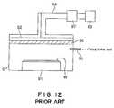
- FIG. 12shows a known microwave plasma processing system for carrying out such a plasma processing process.
- This known microwave plasma processing systemhas a vacuum vessel 9 , a work support table 91 placed in the vacuum vessel 9 to support a wafer W thereon, and a plane slot antenna 92 disposed in an upper region of the interior of the vacuum vessel 9 .
- Microwaves radiated by a microwave power generator 93is fed through a waveguide 94 to the antenna 92 , the microwaves are fed from the antenna 92 to produce a plasma by ionizing a processing gas supplied from a gas supply pipe 95 , and a film is deposited on the surface of the wafer W or the surface of the wafer W is etched with the plasma.
- indicated at 96is a quartz window.
- a load matching device 97is placed on the waveguide 94 to make conjugate the impedance of a section of the waveguide 94 between the load matching device 97 and the plasma and the impedance of a section of the same between the load matching device 97 and the microwave power generator 93 to suppress reflection of the microwave from the plasma.
- the electron density of the plasmais one of factors dominating the condition of the process for processing the wafer W.
- electron densityis substantially equal to plasma density.
- negative ion densityincreases as electron density decreases. Therefore, it is desirable for stable processing to keep electron density constant during the process. However, it is difficult to know electron density and hence it is not easy to control electron density.
- the condition of a plasmais dependent on the microwave power and pressure in the vacuum vessel 9 . Therefore, microwave utilization factor in using a microwave for producing a plasma decreases even if the impedances are matched by the load matching device 97 because some condition of the plasma increases the amount of the microwave reflected by the plasma toward the microwave power generator 93 and the reflected microwave generates heat due to dielectric loss or ohmic loss.
- the present inventionhas been made in view of such problems and it is therefore an object of the present invention to enable monitoring the electron density of a plasma by measuring the reflection coefficient of high-frequency waves, such as microwaves or RF waves, radiated by a power generator.
- a plasma processing methodcomprising the steps of: placing an object to be subjected to a processing into a vacuum vessel; supplying a processing gas into the vacuum vessel; supplying a high-frequency wave into the vacuum vessel from a high-frequency power generator; subjecting the object to the processing by generating a plasma of the processing gas in the vacuum vessel by the high-frequency wave; measuring a state of a reflected high-frequency wave reflected at the plasma, relative to an advancing high-frequency wave travelling toward the plasma; and controlling an electron density of the plasma in response to a measured state of the reflected high-frequency wave.
- a plasma processing apparatuscomprising: a vacuum vessel; a device for supplying a processing gas into the vacuum vessel; a high-frequency power generator for supplying a high-frequency wave into the vacuum vessel to produce plasma of the processing gas; a measuring unit for measuring state of a reflected high-frequency wave reflected at the plasma, relative to an advancing high-frequency wave travelling from the high-frequency power generator toward the plasma; and a control unit for controlling an electron density of the plasma in response to the state of the reflected high-frequency wave measured by the measuring unit.
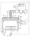
- FIG. 1is a schematic vertical sectional view of a plasma processing apparatus in a first embodiment of the present invention
- FIG. 2is a plan view of an antenna included in the plasma processing apparatus shown in FIG. 1;
- FIG. 3is a diagram for in explaining a conception of reflection coefficient
- FIG. 4is a block diagram of a reflection coefficient measuring unit
- FIG. 5is a schematic vertical sectional view of a plasma processing apparatus in another embodiment of the present invention.
- FIG. 6is a schematic view of a plasma processing apparatus in a further embodiment of the present invention.
- FIG. 7is a Smith chart showing the characteristics of an antenna employed in a plasma processing apparatus in accordance with the present invention.
- FIG. 8is an explanatory view of a Smith chart
- FIG. 9is a Smith chart showing the characteristics of another antenna
- FIG. 10is a view explanatory of the Smith chart shown in FIG. 9;
- FIG. 11is a schematic vertical sectional view of a plasma processing apparatus in a still further embodiment of the present invention.
- FIG. 12is a schematic sectional view of a prior art plasma processing apparatus.
- a wafer table 2 for supporting a wafer W thereinis disposed in a lower region of the interior of a vacuum vessel 1 , and a bias electrode 22 is embedded in the wafer table 2 and is connected to a 13.56 MHz high-frequency power generator 21 .
- the vacuum vessel 1is provided with a temperature regulating unit, not shown.
- a window 11 of a dielectric material, such as quartz,is disposed in the upper region of the interior of the vacuum vessel 1 .
- a plane slot antenna 32 provided with a plurality of slots 31 as shown in FIG. 2is disposed above and opposite to the window 11 .
- One end of a shaft 33 a of a waveguide 33 coaxial with the plane slot antenna 32is connected to the central portion of the plane slot antenna 32 .
- a flat cylindrical part 34 having a, horizontal, annular end wall 34 a and a side wall 34 b extending perpendicularly to the end wallis formed on the lower end of an outer tube 33 b of the waveguide 33 .
- One end of a rectangular waveguide 35is joined to an upper end portion of a side wall of the outer tube 33 b .
- a microwave power generator 4is connected to the other end of the rectangular waveguide 35 .
- a load matching unit 41 and a reflection coefficient measuring unit 5are arranged in this order below the microwave power generator 4 on the waveguide 35 .
- the load matching unit 41operates to match the impedance of a section of the waveguide 35 on the side of a plasma with the impedance of a section of the same on the side of the microwave power generator 4 .
- the reflection coefficient measuring unit 5will be described later in detail.
- a processing gas supply pipe 12is connected to, for example, a side wall of the vacuum vessel 1 .
- silane (SiH 4 ) gasi.e., a film forming gas
- argon (Ar) gasi.e., a carrier gas
- the respective flow rates of SiH 4 gas and argon Ar gasare regulated by a mass-flow regulators F 1 and F 2 , respectively.
- a shower head made of a dielectric material, such as quartz, disposed below the window 11may be used for supplying the processing gas instead of the processing gas supply pipe 12 .
- a discharge pipe 13is connected to the bottom wall of the vacuum vessel 1 and is connected to an evacuating device, not shown, by a pipe provided with a pressure regulator 14 to evacuate the vacuum vessel 1 .
- the pressure in the vacuum vessel 1is regulated by regulating the opening of a butterfly valve by the pressure regulator 14 .
- the reflection coefficient measuring device 5measures voltage reflection coefficient.
- the reflection coefficientis an index of the ratio of reflected electromagnetic waves reflected by a plasma and traveling back toward the microwave power generator 4 to advancing electromagnetic waves traveling from the microwave power generator 4 to the plasma.
- Reflection coefficient ⁇is expressed by Expression (1).
- FIG. 3shows a reflection coefficient in a vector.
- the reflection coefficient measuring unit 5has a directional coupler 51 placed in the waveguide 35 to provide power signals representing the magnitudes of power of the reflected wave and the advancing wave.
- the power signal representing the power of the reflected waveis distributed by a distributor 52 in signals.
- One of the signals distributed by the distributor 52is transferred to a wave detector 53 and a phase shifter 54 .
- the phase shifter 54changes the phase of the power signal by 90° and gives the power signal to a mixer 61 .
- the other signal distributed by the distributor 52is given to a mixer 62 .
- the power signal representing the power of the advancing waveis distributed by a distributor 55 in signals.
- One of the signals distributed by the distributor 55is transferred to a wave detector 56 and the mixer 62 .
- the other signal distributed by the distributor 55is sent to the mixer 61 .
- the detector 53provides the amplitude V r of the reflected wave and the detector 56 provides the amplitude V f of the advancing wave.
- the mixers 61 and 62provide sin ⁇ and cos ⁇ , respectively, where ⁇ is the phase of the reflection coefficient, and an arithmetic unit 64 receives sin ⁇ and cos ⁇ and calculates the phase ⁇ .
- the arithmetic units 63 and 64give calculated values of ⁇ 0 (V r /V f ) and ⁇ to a control unit 7 shown in FIG. 1 .
- the control unit 7controls the output power of the microwave power generator 4 according to the calculated values given thereto. Control procedure to be carried out by the control unit 7 will be described later. Since the load matching unit 41 is liable to disturb the microwave, it is preferable to dispose the reflection coefficient measuring unit 5 downstream from the load matching unit 41 with respect to the direction of propagation of the microwave from the microwave power generator 4 .
- a process of forming a polysilicon film on a wafer by the plasma processing apparatuswill be described hereafter.
- a gate valvenot shown, is opened and a wafer W is placed on the wafer table 2 by a transfer arm, not shown.
- the gate valveis closed, the vacuum vessel 1 is evacuated to a predetermined vacuum of, for example, 10 ⁇ 6 torr.
- a film forming gassuch as SiH 4
- a carrier gassuch as Ar
- the microwave generated by the microwave generator 4propagates through the waveguides 35 and 33 into the flat cylindrical part 34 and propagates through the slots 31 of the antenna 32 into the vacuum vessel 1 to ionize the processing gas supplied into the vacuum vessel 1 .
- Activated radicals and irons produced by ionizing SiH 4are deposited on a surface of the wafer W in a polysilicon film.
- the reflection coefficient measuring unit 5measures the absolute value ⁇ 0 of the reflection coefficient and the phase ⁇ and gives the same to the control unit 7 .
- the antenna 32is designed so that the reflection of the microwave is reduced when the electron density of the plasma is suitable for the film forming process.
- the reflection of the microwaveincreases. If the electron density is not equal to the desired value, the amplitude ⁇ 0 of the reflection coefficient increases.
- the variation of the electron densitycan be detected through monitoring of the absolute value ⁇ 0 , it is impossible to find whether the electron density is increasing or whether the same is decreasing.
- the plasma processing apparatusmonitors also the phase ⁇ of the reflection coefficient to find the directions of change of the electron density.
- the electron density of the plasmabecomes greater than a pre-assumed electron density
- electric currentcan easily flow so that the electric resistance component of the plasma becomes smaller than a pre-assumed value and the phase ⁇ of the reflected wave changes relative to the advancing wave. Consequently, the value ⁇ 0 of the reflection coefficient increases and the phase ⁇ decreases.
- the control unit 7compares the present amounts of the value ⁇ m and the phase ⁇ m with the amounts of the value ⁇ s and the phase ⁇ s either at a time point when the reflection coefficient is stabilized (when the range of variation becomes narrow) for the first time after the production of plasma or at a time point a predetermined time (1 to 5 seconds) after the production of plasma, and the control unit 7 operates to reduce the output of the microwave power generator 4 according to the result of the comparison (differences).
- the control unit 7operates to reduce the output of the microwave power generator 4 according to the result of the comparison (differences).
- the control unit 7controls the microwave power generator 4 so that the output of the microwave power generator 4 increases according to changes in the value ⁇ 0 and the phase ⁇ .
- the power of the microwaveis thus increased, the electron density increases, the value ⁇ 0 decreases and the delay of the phase ⁇ becomes small.
- a change in the electron density of the plasma and the direction of changei.e., increase or decrease, can be known through the measurement of the value ⁇ 0 and the phase ⁇ of the reflection coefficient, and the output of the microwave power generator 4 is controlled according to the measured result.
- the electron density of the plasmais maintained at an appropriate value and a stable film forming process can be achieved. Since the reflected wave is small, power loss is suppressed and an efficient plasma processing can be achieved.
- Means for regulating the electron density of the plasmaneed not be limited to the control of the output of the microwave power generator 4 on the basis of the measured reflection coefficient; the electron density of the plasma may be regulated by controlling any factor that affects the electron density of the plasma.
- the pressure in the vacuum vessel 1may be controlled by the pressure regulator 14 ; the SiH 4 /Ar flow rate ratio may be controlled by adjusting the flow rate of SiH 4 by means of the mass-flow regulator F 1 , by adjusting the flow rate of Ar by means of the mass-flow regulator F 2 or by adjusting the respective flow rates of SiH 4 and Ar by means of the mass-flow regulators F 1 and F 2 ; or the bias power may be controlled by the high-frequency power generator 21 .
- Those control operationsmay be used in combination or the control of microwave power may be used in combination with those control operations.
- the foregoing control operationsare performed so as to reduce the pressure in the vacuum vessel 1 , to reduce the SiH 4 /Ar flow rate ratio and to reduce the bias high-frequency power.
- the distance of the antenna 32i.e., a high-frequency wave radiating unit, fixed to the cylindrical part 34 b relative to the space in the vacuum vessel 1 is controlled on the basis of the measured reflection coefficient.
- the cylindrical part 34 bis moved vertically by a position control motor 73 fixed to the vacuum vessel 1 .
- the motor 73rotates a gear 74 in response to signals from the control unit 7 .
- the gear 74then rotates a screw rod 75 in mesh with the gear 74 .
- the screw rod 75is fixed to the upper surface of the end wall 34 a and causes the antenna 32 to move vertically as a result of rotation of the screw rod 75 , whereby the height of the antenna 32 can be adjusted.
- Numeral 77indicates a shielding member such as a metal bellows, for preventing the leakage of the microwave.
- the shielding member 77connects the side wall 34 b and the vacuum vessel 1 .
- the intensity of an electric field created by an antennadecreases with distance from the antenna. Therefore, the position control motor 73 raises the antenna 32 when the electron density is excessively high.
- control operationis carried out on the basis of changes in the amounts of the value ⁇ 0 and the phase ⁇ at a certain time point
- the foregoing operationmay be carried out on the basis of the result of comparison, i.e., differences, between measured values and predetermined desired values.
- the application of the plasma processing processis not limited to the formation of a polysilicon film, but the plasma processing process may be applied to a processing using a processing gas containing fluorine, such as C 4 F 8 gas, to form a carbon film containing fluorine and to an etching process using CF 4 gas.
- a processing gas containing fluorinesuch as C 4 F 8 gas
- CF 4 gasa processing gas containing fluorine
- radicalsare sputtered from a thin film deposited on the inner surfaces of the vacuum vessel 1 , and electrons and the radicals combine together to produce negative ions. Consequently, the electron density decreases.
- the microwave power generator 4 or a proper factoris controlled to adjust the electron density to an appropriate value.
- process conditions for processing the succeeding wafermay be controlled by taking time-series data on the value ⁇ 0 and the phase ⁇ during the processing of the preceding wafer or a test wafer, storing the time-series data in a storage unit 81 shown FIG. 6, analyzing the stored time-series data and using the results of analysis of the time-series data instead of carrying out the control operation on the basis of data measured by the reflection coefficient measuring unit 5 .
- the output of the microwave power generator 4may be reduced or the control unit 7 may automatically execute the adjustment of the output of the microwave power generator 4 , for example, before the start of processing wafers of a new lot.
- the condition of the plasma processing apparatuscan be known from the data stored in the storage unit 81 .
- abnormal discharge from substances deposited on the inner surface of the vacuum vessel 1 , the thermal deformation of the antenna and an abnormal change in the microwave due to troubles in the electric circuitcan be known from a change in the electron density.
- the control unit 7may monitor the measured data provided by the reflection coefficient measuring unit 5 and may decide that an abnormal condition occurred in the plasma processing apparatus when changes in the value ⁇ 0 and the phase ⁇ from the value ⁇ s and the phase ⁇ s measured at a certain time point and stored in the storage unit 81 have exceeded predetermined levels, respectively, and the control unit 7 may provide warning directions at the warning unit 82 .
- FIG. 7is a Smith chart of reflection coefficient when the microwave power supplied to the antenna 32 shown in FIG. 2 is increased from 0.5 kW toward 2.5 kW.
- the resistance component of an impedance of a section downstream of the reflection coefficient measuring unit 5is measured on the horizontal axis.
- ⁇ 0is the distance from the center, and ⁇ is the angle from the horizontal axis.
- the reflection coefficientvaries along a circular locus that approaches the horizontal axis from below and then recedes from the horizontal axis as shown in FIGS. 9 and 10, which proves that the antenna is not matched.
- An RF power generator or a UHF power generatormay be used instead of the microwave power generator to produce a plasma by ionizing a processing gas.
- the microwave power generator, the RF power generator and the UHF power generatorare designated inclusively as high-frequency power generators.
- Plasmacan also be produced by ionizing the processing gas by means of electron cyclotron resonance caused by a microwave and a magnetic field.
- the vacuum vessel 1is provided with a processing gas supply pipe 12 having a mass-flow regulator F, and a discharge pipe 13 having a pressure regulator 14 .
- a first electrode 81 Asupported on the wall of the vacuum vessel 1 through a dielectric member 82 A.
- a second electrode 81 Bsupported on the wall of the vacuum vessel through a dielectric member 82 B.
- a wafer W to be subjected to the processingis adapted to be put on the second electrode 81 B.
- a reflection coefficient measuring unit 5is connected to the first electrode 81 A, and a control unit 7 is connected to the measuring unit 5 .
- a first load matching unit 41 Awhich is connected to a first RF power generator 84 A.
- a second load matching unit 41 Bwhich is connected to a second RF power generator 84 B.
- Output from the control unit 7is supplied to at least one of the mass-flow regulator F of the processing gas supply pipe 12 , the pressure regulator 14 of the discharge pipe 13 , and the pair of the first and second RF power generators 84 A and 84 B.
- RF waveis produced in the vacuum vessel 1 by the operation of the RF power generators 84 A and 84 B connected to the electrodes 81 A and 81 B, respectively, so that a plasma of the processing gas is generated in the vacuum vessel 1 to thereby carry out a plasma-processing of the workpiece.
- the reflection coefficient measuring unit 5measures the advancing and reflected waves of the RF wave and outputs the amounts of the value ⁇ 0 and the phase ⁇ of the reflection coefficient to send the same to the control unit 7 .
- the control unit 7operates to control a factor influencing the plasma density so as to enable an efficient plasma-processing, in the same manner as in the foregoing embodiments.
- the reflection coefficient measuring unit 5is provided in only the upper RF power generating system, but a reflection coefficient measuring unit and a control unit may be provided between the electrode 81 B and the load matching unit 41 B.
- the present inventioncarries out a plasma-processing of workpieces, by measuring the state of reflection of a high frequency wave due to a plasma produced in the vacuum vessel and by controlling the electron density in the plasma-processing vacuum vessel to a suitable value in response to the detected state of reflection. Therefore, a stable processing is ensured, electric energy loss can be suppressed by reducing the reflection of high-frequency wave, and an efficient plasma-processing is realized.
Landscapes
- Chemical & Material Sciences (AREA)
- Engineering & Computer Science (AREA)
- Physics & Mathematics (AREA)
- Plasma & Fusion (AREA)
- Analytical Chemistry (AREA)
- Materials Engineering (AREA)
- Chemical Kinetics & Catalysis (AREA)
- Mechanical Engineering (AREA)
- Metallurgy (AREA)
- Organic Chemistry (AREA)
- General Chemical & Material Sciences (AREA)
- Plasma Technology (AREA)
- Chemical Vapour Deposition (AREA)
- ing And Chemical Polishing (AREA)
- Drying Of Semiconductors (AREA)
Abstract
Description
Claims (16)
Applications Claiming Priority (4)
| Application Number | Priority Date | Filing Date | Title |
|---|---|---|---|
| JP11-033066 | 1999-02-10 | ||
| JP3306699 | 1999-02-10 | ||
| JP11-326991 | 1999-11-17 | ||
| JP11326991AJP2000299198A (en) | 1999-02-10 | 1999-11-17 | Plasma processing device |
Publications (1)
| Publication Number | Publication Date |
|---|---|
| US6311638B1true US6311638B1 (en) | 2001-11-06 |
Family
ID=26371703
Family Applications (1)
| Application Number | Title | Priority Date | Filing Date |
|---|---|---|---|
| US09/500,520Expired - LifetimeUS6311638B1 (en) | 1999-02-10 | 2000-02-09 | Plasma processing method and apparatus |
Country Status (2)
| Country | Link |
|---|---|
| US (1) | US6311638B1 (en) |
| JP (1) | JP2000299198A (en) |
Cited By (42)
| Publication number | Priority date | Publication date | Assignee | Title |
|---|---|---|---|---|
| US20010019237A1 (en)* | 2000-03-02 | 2001-09-06 | Tokyo Electron Limited | Plasma processing apparatus |
| US20020040765A1 (en)* | 2000-10-06 | 2002-04-11 | Kawasaki Microelectronics Inc. | Apparatus and methods for processing surface of semiconductor substrate |
| US20020104482A1 (en)* | 2001-02-07 | 2002-08-08 | Hideyuki Kazumi | Plasma-assisted processing apparatus |
| WO2002070759A1 (en)* | 2001-02-28 | 2002-09-12 | Commonwealth Scientific And Industrial Research Organisation | Method and apparatus for the production of titanium |
| US6454563B1 (en)* | 2000-08-17 | 2002-09-24 | Samsung Electronics Co., Ltd. | Wafer treatment chamber having thermal reflector |
| US6455814B1 (en)* | 2001-11-07 | 2002-09-24 | Applied Materials, Inc. | Backside heating chamber for emissivity independent thermal processes |
| US20030102083A1 (en)* | 2001-12-05 | 2003-06-05 | Ichiro Sasaki | Apparatus and method for monitoring plasma processing apparatus |
| US20030168172A1 (en)* | 2002-03-11 | 2003-09-11 | Yuri Glukhoy | Plasma treatment apparatus with improved uniformity of treatment and method for improving uniformity of plasma treatment |
| US20030168008A1 (en)* | 2001-03-28 | 2003-09-11 | Tadahiro Ohmi | Plasma processing device |
| US20030194508A1 (en)* | 2002-04-11 | 2003-10-16 | Carpenter Craig M. | Deposition methods utilizing microwave excitation, and deposition apparatuses |
| US6646224B2 (en)* | 1999-06-18 | 2003-11-11 | Tokyo Electron Limited | Plasma-assisted processing system and plasma-assisted processing method |
| US20040045672A1 (en)* | 2001-01-18 | 2004-03-11 | Nobou Ishii | Plasma device and plasma generating method |
| EP1248361A3 (en)* | 2001-04-06 | 2004-03-31 | Eni Technology, Inc. | Device to measure relection coefficient |
| US20040097089A1 (en)* | 2001-03-28 | 2004-05-20 | Tadahiro Ohmi | Device and control method for micro wave plasma processing |
| US20040182702A1 (en)* | 2003-03-21 | 2004-09-23 | Roman Chistyakov | Plasma generation using multi-step ionization |
| US20040244693A1 (en)* | 2001-09-27 | 2004-12-09 | Nobuo Ishii | Electromagnetic field supply apparatus and plasma processing device |
| US20050029954A1 (en)* | 2003-08-06 | 2005-02-10 | Canon Kabushiki Kaisha | Plasma processing apparatus and method |
| US20050034815A1 (en)* | 2001-12-14 | 2005-02-17 | Shigeru Kasai | Plasma processor |
| US6887339B1 (en)* | 2000-09-20 | 2005-05-03 | Applied Science And Technology, Inc. | RF power supply with integrated matching network |
| US20050160986A1 (en)* | 2003-12-10 | 2005-07-28 | Samsung Electronics Co., Ltd. | Electron cyclotron resonance equipment with variable flare angle of horn antenna |
| US20060042546A1 (en)* | 2002-07-24 | 2006-03-02 | Tokyo Electron Limited | Plasma processing apparatus and controlling method therefor |
| EP1347673A4 (en)* | 2000-11-22 | 2006-10-04 | Japan Science & Tech Corp | APPARATUS FOR PRODUCING PLASMA USING MICROWAVE |
| US20070121267A1 (en)* | 2003-11-27 | 2007-05-31 | Hiroyuki Kotani | High-frequency power supply system |
| US20080093024A1 (en)* | 2004-09-06 | 2008-04-24 | Toshiji Abe | Plasma Treating Apparatus |
| US20090238998A1 (en)* | 2008-03-18 | 2009-09-24 | Applied Materials, Inc. | Coaxial microwave assisted deposition and etch systems |
| US20090277778A1 (en)* | 2008-05-06 | 2009-11-12 | Applied Materials, Inc. | Microwave rotatable sputtering deposition |
| US20090283400A1 (en)* | 2008-05-14 | 2009-11-19 | Applied Materials, Inc. | Microwave-assisted rotatable pvd |
| US20100026415A1 (en)* | 2007-02-08 | 2010-02-04 | Huettinger Elektronik Gmbh + Co. Kg | Measuring Power |
| US20100078320A1 (en)* | 2008-09-26 | 2010-04-01 | Applied Materials, Inc. | Microwave plasma containment shield shaping |
| US20100078315A1 (en)* | 2008-09-26 | 2010-04-01 | Applied Materials, Inc. | Microstrip antenna assisted ipvd |
| US20100275981A1 (en)* | 2007-12-19 | 2010-11-04 | Tokyo Electron Limited | Apparatus and method for manufacturing photoelectric conversion elements, and photoelectric conversion element |
| US20110076422A1 (en)* | 2008-01-30 | 2011-03-31 | Applied Materials, Inc. | Curved microwave plasma line source for coating of three-dimensional substrates |
| US20110076420A1 (en)* | 2008-01-30 | 2011-03-31 | Applied Materials, Inc. | High efficiency low energy microwave ion/electron source |
| US20110155057A1 (en)* | 2009-12-25 | 2011-06-30 | Tokyo Electron Limited | Plasma process apparatus |
| US8679594B2 (en) | 2008-02-20 | 2014-03-25 | Applied Materials, Inc. | Index modified coating on polymer substrate |
| TWI450358B (en)* | 2009-01-26 | 2014-08-21 | Mitsubishi Heavy Ind Ltd | A substrate support for a plasma processing device |
| US9018108B2 (en) | 2013-01-25 | 2015-04-28 | Applied Materials, Inc. | Low shrinkage dielectric films |
| US20170345664A1 (en)* | 2014-12-25 | 2017-11-30 | Tokyo Electron Limited | Plasma processing apparatus and plasma processing method |
| US10818478B2 (en) | 2017-03-08 | 2020-10-27 | Tokyo Electron Limited | High frequency generator and plasma processing apparatus |
| CN112447471A (en)* | 2019-09-04 | 2021-03-05 | 中微半导体设备(上海)股份有限公司 | Plasma processing system and operation method thereof |
| US11159878B1 (en)* | 2019-08-15 | 2021-10-26 | Amazon Technologies, Inc. | Autonomously motile device with beamforming |
| US20210351012A1 (en)* | 2020-05-11 | 2021-11-11 | Tokyo Electron Limited | Apparatus and method for plasma processing |
Families Citing this family (14)
| Publication number | Priority date | Publication date | Assignee | Title |
|---|---|---|---|---|
| KR100789796B1 (en)* | 2000-03-30 | 2007-12-31 | 동경 엘렉트론 주식회사 | Plasma processing equipment |
| JP3478266B2 (en)* | 2000-12-04 | 2003-12-15 | 東京エレクトロン株式会社 | Plasma processing equipment |
| JP4481538B2 (en)* | 2001-09-28 | 2010-06-16 | 東京エレクトロン株式会社 | Electromagnetic field supply apparatus and plasma processing apparatus |
| JP4499323B2 (en)* | 2001-09-27 | 2010-07-07 | 東京エレクトロン株式会社 | Electromagnetic field supply apparatus and plasma processing apparatus |
| KR100439749B1 (en)* | 2002-07-29 | 2004-07-12 | 우리로광통신주식회사 | Method for fabricating optical waveguide on fused silica substrates using inductively coupled plasma etcher |
| US7740737B2 (en) | 2004-06-21 | 2010-06-22 | Tokyo Electron Limited | Plasma processing apparatus and method |
| US7951262B2 (en) | 2004-06-21 | 2011-05-31 | Tokyo Electron Limited | Plasma processing apparatus and method |
| TWI574318B (en)* | 2004-06-21 | 2017-03-11 | Tokyo Electron Ltd | A plasma processing apparatus, a plasma processing method, and a computer-readable recording medium |
| US7988816B2 (en) | 2004-06-21 | 2011-08-02 | Tokyo Electron Limited | Plasma processing apparatus and method |
| JP4799947B2 (en)* | 2005-02-25 | 2011-10-26 | 株式会社ダイヘン | High frequency power supply device and control method of high frequency power supply |
| PL2259662T3 (en) | 2008-03-26 | 2019-10-31 | Kyosan Electric Mfg | Abnormal discharge suppressing device for vacuum apparatus |
| JP5411683B2 (en)* | 2009-12-14 | 2014-02-12 | 東京エレクトロン株式会社 | Impedance matching device |
| JP2016092803A (en)* | 2014-11-11 | 2016-05-23 | 三菱重工業株式会社 | Matching circuit and radio communication device |
| JP7125058B2 (en)* | 2018-12-06 | 2022-08-24 | 東京エレクトロン株式会社 | Plasma processing apparatus and plasma processing method |
Citations (6)
| Publication number | Priority date | Publication date | Assignee | Title |
|---|---|---|---|---|
| US5458732A (en)* | 1992-04-14 | 1995-10-17 | Texas Instruments Incorporated | Method and system for identifying process conditions |
| US5472561A (en)* | 1993-12-07 | 1995-12-05 | Sematech, Inc. | Radio frequency monitor for semiconductor process control |
| JPH0963793A (en) | 1995-08-25 | 1997-03-07 | Tokyo Electron Ltd | Plasma processing device |
| US5688357A (en)* | 1995-02-15 | 1997-11-18 | Applied Materials, Inc. | Automatic frequency tuning of an RF power source of an inductively coupled plasma reactor |
| US5698036A (en)* | 1995-05-26 | 1997-12-16 | Tokyo Electron Limited | Plasma processing apparatus |
| US5702562A (en)* | 1995-04-27 | 1997-12-30 | Nec Corporation | Dry etching apparatus and method |
- 1999
- 1999-11-17JPJP11326991Apatent/JP2000299198A/enactivePending
- 2000
- 2000-02-09USUS09/500,520patent/US6311638B1/ennot_activeExpired - Lifetime
Patent Citations (6)
| Publication number | Priority date | Publication date | Assignee | Title |
|---|---|---|---|---|
| US5458732A (en)* | 1992-04-14 | 1995-10-17 | Texas Instruments Incorporated | Method and system for identifying process conditions |
| US5472561A (en)* | 1993-12-07 | 1995-12-05 | Sematech, Inc. | Radio frequency monitor for semiconductor process control |
| US5688357A (en)* | 1995-02-15 | 1997-11-18 | Applied Materials, Inc. | Automatic frequency tuning of an RF power source of an inductively coupled plasma reactor |
| US5702562A (en)* | 1995-04-27 | 1997-12-30 | Nec Corporation | Dry etching apparatus and method |
| US5698036A (en)* | 1995-05-26 | 1997-12-16 | Tokyo Electron Limited | Plasma processing apparatus |
| JPH0963793A (en) | 1995-08-25 | 1997-03-07 | Tokyo Electron Ltd | Plasma processing device |
Cited By (72)
| Publication number | Priority date | Publication date | Assignee | Title |
|---|---|---|---|---|
| US6646224B2 (en)* | 1999-06-18 | 2003-11-11 | Tokyo Electron Limited | Plasma-assisted processing system and plasma-assisted processing method |
| US6670741B2 (en)* | 2000-03-02 | 2003-12-30 | Tokyo Electron Limited | Plasma processing apparatus with annular waveguide |
| US20010019237A1 (en)* | 2000-03-02 | 2001-09-06 | Tokyo Electron Limited | Plasma processing apparatus |
| US6454563B1 (en)* | 2000-08-17 | 2002-09-24 | Samsung Electronics Co., Ltd. | Wafer treatment chamber having thermal reflector |
| US6887339B1 (en)* | 2000-09-20 | 2005-05-03 | Applied Science And Technology, Inc. | RF power supply with integrated matching network |
| US20020040765A1 (en)* | 2000-10-06 | 2002-04-11 | Kawasaki Microelectronics Inc. | Apparatus and methods for processing surface of semiconductor substrate |
| US6815369B2 (en) | 2000-10-06 | 2004-11-09 | Kawasaki Microelectronics Inc. | Method for monitoring deposition reaction during processing the surface of a semiconductor substrate |
| EP1347673A4 (en)* | 2000-11-22 | 2006-10-04 | Japan Science & Tech Corp | APPARATUS FOR PRODUCING PLASMA USING MICROWAVE |
| US20040045672A1 (en)* | 2001-01-18 | 2004-03-11 | Nobou Ishii | Plasma device and plasma generating method |
| US6911617B2 (en)* | 2001-01-18 | 2005-06-28 | Tokyo Electron Limited | Plasma device and plasma generating method |
| US6793768B2 (en)* | 2001-02-07 | 2004-09-21 | Hitachi, Ltd. | Plasma-assisted processing apparatus |
| US20020104482A1 (en)* | 2001-02-07 | 2002-08-08 | Hideyuki Kazumi | Plasma-assisted processing apparatus |
| WO2002070759A1 (en)* | 2001-02-28 | 2002-09-12 | Commonwealth Scientific And Industrial Research Organisation | Method and apparatus for the production of titanium |
| US7404991B2 (en)* | 2001-03-28 | 2008-07-29 | Tokyo Electron Limited | Device and control method for micro wave plasma processing |
| US20030168008A1 (en)* | 2001-03-28 | 2003-09-11 | Tadahiro Ohmi | Plasma processing device |
| US20040097089A1 (en)* | 2001-03-28 | 2004-05-20 | Tadahiro Ohmi | Device and control method for micro wave plasma processing |
| US20060118241A1 (en)* | 2001-03-28 | 2006-06-08 | Tadahiro Ohmi & Tokyo Electron Limited | Plasma processing apparatus |
| US7670454B2 (en) | 2001-03-28 | 2010-03-02 | Tokyo Electron Limited | Plasma processing apparatus |
| EP1248361A3 (en)* | 2001-04-06 | 2004-03-31 | Eni Technology, Inc. | Device to measure relection coefficient |
| US20040244693A1 (en)* | 2001-09-27 | 2004-12-09 | Nobuo Ishii | Electromagnetic field supply apparatus and plasma processing device |
| US6455814B1 (en)* | 2001-11-07 | 2002-09-24 | Applied Materials, Inc. | Backside heating chamber for emissivity independent thermal processes |
| US6796269B2 (en)* | 2001-12-05 | 2004-09-28 | Hitchi High-Technologies Corporation | Apparatus and method for monitoring plasma processing apparatus |
| US20030102083A1 (en)* | 2001-12-05 | 2003-06-05 | Ichiro Sasaki | Apparatus and method for monitoring plasma processing apparatus |
| US20050051270A1 (en)* | 2001-12-05 | 2005-03-10 | Ichiro Sasaki | Method for monitoring plasma processing apparatus |
| US7226524B2 (en)* | 2001-12-14 | 2007-06-05 | Tokyo Electron Limited | Plasma processing apparatus |
| US20050034815A1 (en)* | 2001-12-14 | 2005-02-17 | Shigeru Kasai | Plasma processor |
| US20030168172A1 (en)* | 2002-03-11 | 2003-09-11 | Yuri Glukhoy | Plasma treatment apparatus with improved uniformity of treatment and method for improving uniformity of plasma treatment |
| US6783629B2 (en)* | 2002-03-11 | 2004-08-31 | Yuri Glukhoy | Plasma treatment apparatus with improved uniformity of treatment and method for improving uniformity of plasma treatment |
| US20070036895A1 (en)* | 2002-04-11 | 2007-02-15 | Carpenter Craig M | Deposition methods utilizing microwave excitation |
| US20040089233A1 (en)* | 2002-04-11 | 2004-05-13 | Carpenter Craig M. | Deposition methods utilizing microwave excitation |
| US7105208B2 (en) | 2002-04-11 | 2006-09-12 | Micron Technology, Inc. | Methods and processes utilizing microwave excitation |
| US6845734B2 (en)* | 2002-04-11 | 2005-01-25 | Micron Technology, Inc. | Deposition apparatuses configured for utilizing phased microwave radiation |
| US20030194508A1 (en)* | 2002-04-11 | 2003-10-16 | Carpenter Craig M. | Deposition methods utilizing microwave excitation, and deposition apparatuses |
| US7422986B2 (en) | 2002-04-11 | 2008-09-09 | Micron Technology, Inc. | Deposition methods utilizing microwave excitation |
| US20060042546A1 (en)* | 2002-07-24 | 2006-03-02 | Tokyo Electron Limited | Plasma processing apparatus and controlling method therefor |
| US20050034666A1 (en)* | 2003-03-21 | 2005-02-17 | Roman Chistyakov | Plasma generation using multi-step ionization |
| US6805779B2 (en)* | 2003-03-21 | 2004-10-19 | Zond, Inc. | Plasma generation using multi-step ionization |
| US20040182702A1 (en)* | 2003-03-21 | 2004-09-23 | Roman Chistyakov | Plasma generation using multi-step ionization |
| US20050029954A1 (en)* | 2003-08-06 | 2005-02-10 | Canon Kabushiki Kaisha | Plasma processing apparatus and method |
| KR100980598B1 (en) | 2003-11-27 | 2010-09-07 | 가부시키가이샤 다이헨 | High frequency power supply system |
| US8134816B2 (en) | 2003-11-27 | 2012-03-13 | Daihen Corporation | High-frequency power supply system |
| US20100277843A1 (en)* | 2003-11-27 | 2010-11-04 | Daihen Corporation | High-frequency power supply system |
| US20070121267A1 (en)* | 2003-11-27 | 2007-05-31 | Hiroyuki Kotani | High-frequency power supply system |
| US7796368B2 (en)* | 2003-11-27 | 2010-09-14 | Daihen Corporation | High-frequency power supply system |
| US20050160986A1 (en)* | 2003-12-10 | 2005-07-28 | Samsung Electronics Co., Ltd. | Electron cyclotron resonance equipment with variable flare angle of horn antenna |
| US7410552B2 (en)* | 2003-12-10 | 2008-08-12 | Samsung Electronics Co., Ltd | Electron cyclotron resonance equipment with variable flare angle of horn antenna |
| US20080093024A1 (en)* | 2004-09-06 | 2008-04-24 | Toshiji Abe | Plasma Treating Apparatus |
| US8267041B2 (en)* | 2004-09-06 | 2012-09-18 | Tokyo Electron Limited | Plasma treating apparatus |
| US20100026415A1 (en)* | 2007-02-08 | 2010-02-04 | Huettinger Elektronik Gmbh + Co. Kg | Measuring Power |
| US8203398B2 (en) | 2007-02-08 | 2012-06-19 | Huettinger Elektronik Gmbh + Co. Kg | Measuring power |
| US20100275981A1 (en)* | 2007-12-19 | 2010-11-04 | Tokyo Electron Limited | Apparatus and method for manufacturing photoelectric conversion elements, and photoelectric conversion element |
| US20110076422A1 (en)* | 2008-01-30 | 2011-03-31 | Applied Materials, Inc. | Curved microwave plasma line source for coating of three-dimensional substrates |
| US20110076420A1 (en)* | 2008-01-30 | 2011-03-31 | Applied Materials, Inc. | High efficiency low energy microwave ion/electron source |
| US20110097517A1 (en)* | 2008-01-30 | 2011-04-28 | Applied Materials, Inc. | Dynamic vertical microwave deposition of dielectric layers |
| US8679594B2 (en) | 2008-02-20 | 2014-03-25 | Applied Materials, Inc. | Index modified coating on polymer substrate |
| US20090238998A1 (en)* | 2008-03-18 | 2009-09-24 | Applied Materials, Inc. | Coaxial microwave assisted deposition and etch systems |
| US20090277778A1 (en)* | 2008-05-06 | 2009-11-12 | Applied Materials, Inc. | Microwave rotatable sputtering deposition |
| US8057649B2 (en) | 2008-05-06 | 2011-11-15 | Applied Materials, Inc. | Microwave rotatable sputtering deposition |
| US20090283400A1 (en)* | 2008-05-14 | 2009-11-19 | Applied Materials, Inc. | Microwave-assisted rotatable pvd |
| US8349156B2 (en) | 2008-05-14 | 2013-01-08 | Applied Materials, Inc. | Microwave-assisted rotatable PVD |
| US20100078315A1 (en)* | 2008-09-26 | 2010-04-01 | Applied Materials, Inc. | Microstrip antenna assisted ipvd |
| US20100078320A1 (en)* | 2008-09-26 | 2010-04-01 | Applied Materials, Inc. | Microwave plasma containment shield shaping |
| TWI450358B (en)* | 2009-01-26 | 2014-08-21 | Mitsubishi Heavy Ind Ltd | A substrate support for a plasma processing device |
| US20110155057A1 (en)* | 2009-12-25 | 2011-06-30 | Tokyo Electron Limited | Plasma process apparatus |
| US9018108B2 (en) | 2013-01-25 | 2015-04-28 | Applied Materials, Inc. | Low shrinkage dielectric films |
| US20170345664A1 (en)* | 2014-12-25 | 2017-11-30 | Tokyo Electron Limited | Plasma processing apparatus and plasma processing method |
| US10672616B2 (en)* | 2014-12-25 | 2020-06-02 | Tokyo Electon Limited | Plasma processing apparatus and plasma processing method |
| US10818478B2 (en) | 2017-03-08 | 2020-10-27 | Tokyo Electron Limited | High frequency generator and plasma processing apparatus |
| US11159878B1 (en)* | 2019-08-15 | 2021-10-26 | Amazon Technologies, Inc. | Autonomously motile device with beamforming |
| CN112447471A (en)* | 2019-09-04 | 2021-03-05 | 中微半导体设备(上海)股份有限公司 | Plasma processing system and operation method thereof |
| US20210351012A1 (en)* | 2020-05-11 | 2021-11-11 | Tokyo Electron Limited | Apparatus and method for plasma processing |
| US11646178B2 (en)* | 2020-05-11 | 2023-05-09 | Tokyo Electron Limited | Apparatus for plasma processing |
Also Published As
| Publication number | Publication date |
|---|---|
| JP2000299198A (en) | 2000-10-24 |
Similar Documents
| Publication | Publication Date | Title |
|---|---|---|
| US6311638B1 (en) | Plasma processing method and apparatus | |
| US12068208B2 (en) | Plasma processing apparatus and control method | |
| US10971413B2 (en) | Plasma processing apparatus and control method | |
| US8241457B2 (en) | Plasma processing system, plasma measurement system, plasma measurement method, and plasma control system | |
| US11037761B2 (en) | Control method and plasma processing apparatus | |
| KR101711667B1 (en) | Automatic matching unit and plasma processing apparatus | |
| US6172321B1 (en) | Method and apparatus for plasma processing apparatus | |
| US5471115A (en) | Method and apparatus for measuring electron density of plasma | |
| US7404991B2 (en) | Device and control method for micro wave plasma processing | |
| US20040060660A1 (en) | Control of plasma density with broadband RF sensor | |
| KR101290676B1 (en) | Plasma processing apparatus and plasma processing method | |
| JP2001203097A (en) | Plasma density measuring apparatus and method, and plasma processing apparatus and method using the same | |
| US11031213B2 (en) | Microwave output device and plasma processing device | |
| KR20160110207A (en) | Microwave automatic matcher and plasma processing apparatus | |
| CN101128084B (en) | Plasma generation device, plasma control method, and substrate manufacturing method | |
| US20230106303A1 (en) | Plasma processing apparatus and plasma processing method | |
| US20250006464A1 (en) | Plasma processing apparatus, analysis apparatus, and storage medium | |
| JP7374023B2 (en) | Inspection method and plasma processing equipment | |
| US20040051464A1 (en) | Plasma device and plasma generating method | |
| JP2001007089A (en) | Plasma processing method and apparatus | |
| JP3732287B2 (en) | Plasma processing equipment | |
| US20210305030A1 (en) | Substrate processing device, substrate processing system, control method for substrate processing device, and control method for substrate processing system | |
| US20230326719A1 (en) | Film forming method and film forming apparatus |
Legal Events
| Date | Code | Title | Description |
|---|---|---|---|
| AS | Assignment | Owner name:TOKYO ELECTRON LIMITED, JAPAN Free format text:ASSIGNMENT OF ASSIGNORS INTEREST;ASSIGNORS:ISHII, NOBUO;YASAKA, YASUYOSHI;ANDO, MAKOTO;AND OTHERS;REEL/FRAME:010863/0400;SIGNING DATES FROM 20000420 TO 20000425 Owner name:YASAKA, YASUYOSHI, JAPAN Free format text:ASSIGNMENT OF ASSIGNORS INTEREST;ASSIGNORS:ISHII, NOBUO;YASAKA, YASUYOSHI;ANDO, MAKOTO;AND OTHERS;REEL/FRAME:010863/0400;SIGNING DATES FROM 20000420 TO 20000425 Owner name:ANDO, MAKOTO, JAPAN Free format text:ASSIGNMENT OF ASSIGNORS INTEREST;ASSIGNORS:ISHII, NOBUO;YASAKA, YASUYOSHI;ANDO, MAKOTO;AND OTHERS;REEL/FRAME:010863/0400;SIGNING DATES FROM 20000420 TO 20000425 Owner name:GOTO, NAOHISA, JAPAN Free format text:ASSIGNMENT OF ASSIGNORS INTEREST;ASSIGNORS:ISHII, NOBUO;YASAKA, YASUYOSHI;ANDO, MAKOTO;AND OTHERS;REEL/FRAME:010863/0400;SIGNING DATES FROM 20000420 TO 20000425 | |
| AS | Assignment | Owner name:TOKYO ELECTRON LIMITED, JAPAN Free format text:ASSIGNMENT OF ASSIGNORS INTEREST;ASSIGNORS:ISHII, NOBUO;YASAKA, YASUYOSHI;ANDO, MAKOTO;AND OTHERS;REEL/FRAME:012027/0818;SIGNING DATES FROM 20010710 TO 20010713 Owner name:YASAKA, YASUYOSHI, JAPAN Free format text:ASSIGNMENT OF ASSIGNORS INTEREST;ASSIGNORS:ISHII, NOBUO;YASAKA, YASUYOSHI;ANDO, MAKOTO;AND OTHERS;REEL/FRAME:012027/0818;SIGNING DATES FROM 20010710 TO 20010713 Owner name:ANDO, MAKOTO, JAPAN Free format text:ASSIGNMENT OF ASSIGNORS INTEREST;ASSIGNORS:ISHII, NOBUO;YASAKA, YASUYOSHI;ANDO, MAKOTO;AND OTHERS;REEL/FRAME:012027/0818;SIGNING DATES FROM 20010710 TO 20010713 Owner name:GOTO, NAOHISA, JAPAN Free format text:ASSIGNMENT OF ASSIGNORS INTEREST;ASSIGNORS:ISHII, NOBUO;YASAKA, YASUYOSHI;ANDO, MAKOTO;AND OTHERS;REEL/FRAME:012027/0818;SIGNING DATES FROM 20010710 TO 20010713 | |
| STCF | Information on status: patent grant | Free format text:PATENTED CASE | |
| FPAY | Fee payment | Year of fee payment:4 | |
| FPAY | Fee payment | Year of fee payment:8 | |
| FPAY | Fee payment | Year of fee payment:12 |