US6311016B1 - Substrate temperature measuring apparatus, substrate temperature measuring method, substrate heating method and heat treatment apparatus - Google Patents
Substrate temperature measuring apparatus, substrate temperature measuring method, substrate heating method and heat treatment apparatusDownload PDFInfo
- Publication number
- US6311016B1 US6311016B1US09/171,786US17178699AUS6311016B1US 6311016 B1US6311016 B1US 6311016B1US 17178699 AUS17178699 AUS 17178699AUS 6311016 B1US6311016 B1US 6311016B1
- Authority
- US
- United States
- Prior art keywords
- temperature measuring
- substrate
- temperature
- covering member
- covering
- Prior art date
- Legal status (The legal status is an assumption and is not a legal conclusion. Google has not performed a legal analysis and makes no representation as to the accuracy of the status listed.)
- Expired - Fee Related
Links
- 239000000758substrateSubstances0.000titleclaimsabstractdescription231
- 238000010438heat treatmentMethods0.000titleclaimsabstractdescription67
- 238000000034methodMethods0.000titleclaimsabstractdescription55
- 239000000463materialSubstances0.000claimsabstractdescription64
- 230000005540biological transmissionEffects0.000claimsdescription13
- 230000005855radiationEffects0.000claimsdescription13
- HBMJWWWQQXIZIP-UHFFFAOYSA-Nsilicon carbideChemical compound[Si+]#[C-]HBMJWWWQQXIZIP-UHFFFAOYSA-N0.000claimsdescription12
- 229910010271silicon carbideInorganic materials0.000claimsdescription11
- PNEYBMLMFCGWSK-UHFFFAOYSA-Naluminium oxideInorganic materials[O-2].[O-2].[O-2].[Al+3].[Al+3]PNEYBMLMFCGWSK-UHFFFAOYSA-N0.000claimsdescription8
- 229910021332silicideInorganic materials0.000claimsdescription6
- FVBUAEGBCNSCDD-UHFFFAOYSA-Nsilicide(4-)Chemical compound[Si-4]FVBUAEGBCNSCDD-UHFFFAOYSA-N0.000claimsdescription6
- PMHQVHHXPFUNSP-UHFFFAOYSA-Mcopper(1+);methylsulfanylmethane;bromideChemical compoundBr[Cu].CSCPMHQVHHXPFUNSP-UHFFFAOYSA-M0.000claimsdescription4
- 239000004065semiconductorSubstances0.000claimsdescription4
- 230000003287optical effectEffects0.000claimsdescription3
- 238000005259measurementMethods0.000abstractdescription30
- XUIMIQQOPSSXEZ-UHFFFAOYSA-NSiliconChemical compound[Si]XUIMIQQOPSSXEZ-UHFFFAOYSA-N0.000description51
- 229910052710siliconInorganic materials0.000description51
- 239000010703siliconSubstances0.000description51
- 238000011156evaluationMethods0.000description40
- 238000010586diagramMethods0.000description20
- VYPSYNLAJGMNEJ-UHFFFAOYSA-Nsilicon dioxideInorganic materialsO=[Si]=OVYPSYNLAJGMNEJ-UHFFFAOYSA-N0.000description14
- 239000010453quartzSubstances0.000description13
- 230000031700light absorptionEffects0.000description12
- 238000004151rapid thermal annealingMethods0.000description11
- 238000010521absorption reactionMethods0.000description9
- BASFCYQUMIYNBI-UHFFFAOYSA-NplatinumChemical compound[Pt]BASFCYQUMIYNBI-UHFFFAOYSA-N0.000description9
- 238000006243chemical reactionMethods0.000description6
- OKZIUSOJQLYFSE-UHFFFAOYSA-NdifluoroboronChemical compoundF[B]FOKZIUSOJQLYFSE-UHFFFAOYSA-N0.000description6
- 239000004020conductorSubstances0.000description5
- 239000012535impuritySubstances0.000description5
- 230000000694effectsEffects0.000description4
- 238000009413insulationMethods0.000description4
- 238000005468ion implantationMethods0.000description4
- 239000010948rhodiumSubstances0.000description4
- 229910045601alloyInorganic materials0.000description3
- 239000000956alloySubstances0.000description3
- 238000009529body temperature measurementMethods0.000description3
- 230000000052comparative effectEffects0.000description3
- 229910052736halogenInorganic materials0.000description3
- 150000002367halogensChemical class0.000description3
- 229910052697platinumInorganic materials0.000description3
- 230000004043responsivenessEffects0.000description3
- 229910052703rhodiumInorganic materials0.000description3
- MHOVAHRLVXNVSD-UHFFFAOYSA-Nrhodium atomChemical compound[Rh]MHOVAHRLVXNVSD-UHFFFAOYSA-N0.000description3
- YXTPWUNVHCYOSP-UHFFFAOYSA-Nbis($l^{2}-silanylidene)molybdenumChemical compound[Si]=[Mo]=[Si]YXTPWUNVHCYOSP-UHFFFAOYSA-N0.000description2
- 229910017052cobaltInorganic materials0.000description2
- 239000010941cobaltSubstances0.000description2
- GUTLYIVDDKVIGB-UHFFFAOYSA-Ncobalt atomChemical compound[Co]GUTLYIVDDKVIGB-UHFFFAOYSA-N0.000description2
- 238000011109contaminationMethods0.000description2
- 230000006866deteriorationEffects0.000description2
- 239000006185dispersionSubstances0.000description2
- 238000002474experimental methodMethods0.000description2
- 230000001678irradiating effectEffects0.000description2
- 238000004519manufacturing processMethods0.000description2
- 229910052751metalInorganic materials0.000description2
- 239000002184metalSubstances0.000description2
- 229910021344molybdenum silicideInorganic materials0.000description2
- 238000012856packingMethods0.000description2
- 229910021341titanium silicideInorganic materials0.000description2
- 238000002834transmittanceMethods0.000description2
- 239000000654additiveSubstances0.000description1
- 239000000853adhesiveSubstances0.000description1
- 230000001070adhesive effectEffects0.000description1
- 238000000137annealingMethods0.000description1
- 238000001816coolingMethods0.000description1
- 239000013078crystalSubstances0.000description1
- 230000007547defectEffects0.000description1
- 230000001419dependent effectEffects0.000description1
- 238000005516engineering processMethods0.000description1
- 238000003754machiningMethods0.000description1
- 230000035515penetrationEffects0.000description1
Images


Classifications
- G—PHYSICS
- G01—MEASURING; TESTING
- G01K—MEASURING TEMPERATURE; MEASURING QUANTITY OF HEAT; THERMALLY-SENSITIVE ELEMENTS NOT OTHERWISE PROVIDED FOR
- G01K13/00—Thermometers specially adapted for specific purposes
- G—PHYSICS
- G01—MEASURING; TESTING
- G01K—MEASURING TEMPERATURE; MEASURING QUANTITY OF HEAT; THERMALLY-SENSITIVE ELEMENTS NOT OTHERWISE PROVIDED FOR
- G01K1/00—Details of thermometers not specially adapted for particular types of thermometer
- G01K1/16—Special arrangements for conducting heat from the object to the sensitive element
- G—PHYSICS
- G01—MEASURING; TESTING
- G01K—MEASURING TEMPERATURE; MEASURING QUANTITY OF HEAT; THERMALLY-SENSITIVE ELEMENTS NOT OTHERWISE PROVIDED FOR
- G01K1/00—Details of thermometers not specially adapted for particular types of thermometer
- G01K1/14—Supports; Fastening devices; Arrangements for mounting thermometers in particular locations
- G01K1/143—Supports; Fastening devices; Arrangements for mounting thermometers in particular locations for measuring surface temperatures
- G—PHYSICS
- G01—MEASURING; TESTING
- G01K—MEASURING TEMPERATURE; MEASURING QUANTITY OF HEAT; THERMALLY-SENSITIVE ELEMENTS NOT OTHERWISE PROVIDED FOR
- G01K1/00—Details of thermometers not specially adapted for particular types of thermometer
- G01K1/20—Compensating for effects of temperature changes other than those to be measured, e.g. changes in ambient temperature
- H—ELECTRICITY
- H01—ELECTRIC ELEMENTS
- H01L—SEMICONDUCTOR DEVICES NOT COVERED BY CLASS H10
- H01L21/00—Processes or apparatus adapted for the manufacture or treatment of semiconductor or solid state devices or of parts thereof
- H01L21/02—Manufacture or treatment of semiconductor devices or of parts thereof
- H01L21/04—Manufacture or treatment of semiconductor devices or of parts thereof the devices having potential barriers, e.g. a PN junction, depletion layer or carrier concentration layer
- H01L21/18—Manufacture or treatment of semiconductor devices or of parts thereof the devices having potential barriers, e.g. a PN junction, depletion layer or carrier concentration layer the devices having semiconductor bodies comprising elements of Group IV of the Periodic Table or AIIIBV compounds with or without impurities, e.g. doping materials
- H01L21/26—Bombardment with radiation
- H—ELECTRICITY
- H01—ELECTRIC ELEMENTS
- H01L—SEMICONDUCTOR DEVICES NOT COVERED BY CLASS H10
- H01L21/00—Processes or apparatus adapted for the manufacture or treatment of semiconductor or solid state devices or of parts thereof
- H01L21/02—Manufacture or treatment of semiconductor devices or of parts thereof
- H01L21/04—Manufacture or treatment of semiconductor devices or of parts thereof the devices having potential barriers, e.g. a PN junction, depletion layer or carrier concentration layer
- H01L21/18—Manufacture or treatment of semiconductor devices or of parts thereof the devices having potential barriers, e.g. a PN junction, depletion layer or carrier concentration layer the devices having semiconductor bodies comprising elements of Group IV of the Periodic Table or AIIIBV compounds with or without impurities, e.g. doping materials
- H01L21/30—Treatment of semiconductor bodies using processes or apparatus not provided for in groups H01L21/20 - H01L21/26
- H01L21/324—Thermal treatment for modifying the properties of semiconductor bodies, e.g. annealing, sintering
- H—ELECTRICITY
- H01—ELECTRIC ELEMENTS
- H01L—SEMICONDUCTOR DEVICES NOT COVERED BY CLASS H10
- H01L21/00—Processes or apparatus adapted for the manufacture or treatment of semiconductor or solid state devices or of parts thereof
- H01L21/67—Apparatus specially adapted for handling semiconductor or electric solid state devices during manufacture or treatment thereof; Apparatus specially adapted for handling wafers during manufacture or treatment of semiconductor or electric solid state devices or components ; Apparatus not specifically provided for elsewhere
- H01L21/67005—Apparatus not specifically provided for elsewhere
- H01L21/67011—Apparatus for manufacture or treatment
- H01L21/67098—Apparatus for thermal treatment
- H01L21/67115—Apparatus for thermal treatment mainly by radiation
- H—ELECTRICITY
- H01—ELECTRIC ELEMENTS
- H01L—SEMICONDUCTOR DEVICES NOT COVERED BY CLASS H10
- H01L21/00—Processes or apparatus adapted for the manufacture or treatment of semiconductor or solid state devices or of parts thereof
- H01L21/67—Apparatus specially adapted for handling semiconductor or electric solid state devices during manufacture or treatment thereof; Apparatus specially adapted for handling wafers during manufacture or treatment of semiconductor or electric solid state devices or components ; Apparatus not specifically provided for elsewhere
- H01L21/67005—Apparatus not specifically provided for elsewhere
- H01L21/67242—Apparatus for monitoring, sorting or marking
- H01L21/67248—Temperature monitoring
Definitions
- This inventionrelates to a substrate temperature measuring apparatus, a substrate temperature measuring method, a substrate heating method and a heating method apparatus.
- RTARapid Thermal Annealing
- the substrate heating methodemploys light irradiation
- the temperature of the substratechanges depending on a change in the light transmission factor of the quartz tube which is employed as the heating apparatus, a change in a reflection factor of the inside wall of the chamber, and a change in the lamp output in terms of time and the like.
- closed loop controlis under discussion which measures the substrate temperature and feeds back the measured value to control the lamp output is under discussion.
- thermometerAlso, one apparatus for measuring the substrate temperature, there is a radiation thermometer.
- This radiation thermometerhas an advantage in that it can carry out the temperature measurement of the substrate without coming in contact therewith.
- thermocoupleAnother temperature measuring apparatus is a thermocouple.
- a thermocoupleWhen the temperature measurement is carried out by a thermocouple, there are methods to get the thermocouple in direct contact with a surface of the substrate and to fix the thermocouple on the surface of the substrate by using a thermally stabilized adhesive, and so on. These methods have advantage in that when the temperature measuring portion (alloy portion) of the thermocouple comes in direct contact with the substrate it is possible to accurately measure the substrate temperature.
- thermocoupleAs for other temperature measuring apparatuses, an apparatus is disclosed in a Japanese patent application No 4148546 public bulletin, wherein the substrate temperature is indirectly measured by inserting the thermocouple into a covering member made of silicon carbide (SiC).
- Temperature measurements made by using the above-mentioned radiation thermometerare different from the contact-type heat measuring method using thermocouples in that its measuring accuracy depends on the surface state of the object to be measured and hence, is strongly influenced by a measuring environment.
- substrates having various film structures and impurity concentrationsthere is different emissivity for every substrate. Accordingly, as there is a need to first obtain the emissivity of each substrate in order to carry out an accurate measurement.
- thermocouplein direct contact with the substrate, problems occur with the deterioration in the thermocouple due to a reaction between the substrate and the thermocouple, metal contamination of the substrate, and the like.
- thermocoupleis measuring the temperature of the covering member. Also, in a process wherein the substrate is subjected to heating by light irradiation heating apparatus, when the substrate temperature rises, the covering member is heated not only by thermal conduction, but by directly absorbing the irradiated light. As a result, the accurate measurement of the substrate temperature becomes difficult.
- the heat conduction from the substrate, absorption of radiation from the substrate by the covering member, and absorption of the irradiated lamp lightdiffer depending on materials used for the covering member. Quartz and silicon carbide are shown as examples. When the quarts is used for the covering member, the light absorption can be restrained, but because the quartz has body heat conduction, the measurement of the substrate temperature is difficult and its thermal responsiveness deteriorates. On the other hand, when silicon carbide is used for the covering member, it excels in conducting substrate, heat but, because it absorbs a great deal of light, the measured temperature depends greatly on the light irradiation intensity. Due to these thermal characteristics, each of the materials has advantages as well as a drawback.
- Another method to increase thermal conduction efficiency from the substrateemploys machining the covering member flat at a contact portion between the covering member and the substrate , where two surfaces are in contact with each other, but this method leads to increasing the thermal capacity of the covering member. As a result, there is increased heating due to the direct absorption of light, thereby making it impossible to accurately measure the substrate temperature.
- thermocoupleBecause a portion of the thermocouple, other than a point where the temperature is measured is heated, there is a concern that a high temperature region will occur in an middle region with respect to the “temperature measuring point”, thereby inviting a shunt error, which drops the accuracy of the measurement.
- the present inventionprovides a substrate temperature measuring apparatus, a substrate temperature measuring method, a substrate heating method and a heating method apparatus with a view to solving the above-mentioned problems.
- the substrate temperature measuring apparatusis equipped with a temperature measuring means and a covering member and the temperature measuring means measures the temperature of a substrate which is heated by light irradiation by contacting a temperature measuring portion of the temperature measuring means to the substrate through the covering member.
- a portion in the covering member that covers the measuring portionis made of a material having high heat conductivity.
- the other portion of the covering member which does not cover the measuring portionconsists of a material having high heat conductivity and is made of either a material having a high light transmittance factor or a material having a high light reflection factor.
- the portion of the covering member covering the temperature measuring portion of the temperature measuring apparatusis made of a material with high heat conductivity, the substrate temperature tends to easily conduct to the temperature measuring portion. As a result, although it is a measurement of the temperature through the covering member, it becomes possible to measure the substrate temperature. Also, because the portion of the covering member not covering the measuring portion is made of a material having high heat conductivity with a high light transmission factor or material with the high reflection factor, the covering material covering the temperature measuring means never absorbs the light when subjected to the light irradiation in the midst of measuring.
- a method for measuring the substrate temperatureemploys the above-described temperature measuring means and the covering member for covering it, for measuring the temperature of the substrate.
- the substrateis heated by light irradiation with the substrate temperature being measured by having the measuring portion of the temperature measuring means in contact with the substrate through the covering member.
- the temperature of the substrateis measured by the covering member which is made of a material with a high heat conductivity, the temperature of the substrate is easily conducted to the heat-measuring unit by the covering member. As a result, although it is the measurement of the temperature of the covering member, it becomes possible to accurately measure the substrate temperature. Because a portion of the covering member is made of either a material having a high light transmittance factor or a material having a high light reflecting factor, the covering material almost never absorbs light when subjected to the light irradiation in the midst of measuring.
- a method for heating a substrate by way of light irradiationis a method wherein the light irradiation is conducted by raising an irradiation intensity of a light which is irradiated upon a substrate surface on the opposite side of a substrate from with which the temperature measuring portion of the temperature measuring apparatus for measuring the substrate temperature is in contact.
- the intensity of the light irradiated on the substrate surface on the side with which the temperature measuring portion is in contactis weakened, i.e., a quantity of the light irradiated on the temperature measuring portion becomes smaller.
- a quantity of the light irradiated on the temperature measuring portionbecomes smaller.
- a heating method apparatusis equipped with a heating light source by way of the light irradiation, a member to be irradiated by the light from the heating light source, a temperature measuring portion for measuring the temperature of the heated member, a first temperature measuring portion covering member which is provided at one end of the temperature measuring portion and made of the material having high heat conductivity, and a second temperature measuring portion covering member which covers a periphery of the temperature measuring portion and is made of a material having a high light transmission factor.
- the first temperature measuring portion covering member for covering the temperature measuring portionis made of the material having high heat conductivity
- the substrate temperaturetends to easily conduct to the temperature measuring portion. For that reason, although it is the measurement of the temperature through the first temperature measuring portion covering member, it becomes possible to measure the substrate temperature.
- the second temperature measuring portion covering memberis made of a material having high heat conductivity and with a high light transmission factor or a material with a high light reflection factor, when this portion is subjected to the light irradiation, it almost never absorbs the light.
- FIG. 1is a schematic structural cross-sectional diagram of a first embodiment of the invention in connection with a temperature measuring apparatus of the present invention
- FIG. 2is a schematic structural cross-sectional diagram of one example of a light irradiation-type heating method apparatus using the temperature measuring apparatus;
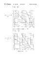
- FIG. 3is a schematic structural cross-sectional diagram of each of evaluation samples
- FIG. 4is an explanatory diagram of a sequence of RTA
- FIG. 5is a diagram showing the relationship between a sheet resistance of the respective evaluation samples and a set temperature of the RTA;
- FIG. 6is a diagram showing the relationship between a measured temperature by the temperature measuring apparatus of the present invention and the sheet resistance
- FIG. 7is a schematic structural cross-sectional diagram of the temperature measuring apparatus of a comparative example
- FIG. 8is a diagram showing relations between the measured temperature by the temperature measuring apparatus of the comparative example and the sheet resistance
- FIG. 9is a diagram showing the relationship between the sheet resistance of a third evaluation sample and a thickness of an oxidized silicon film
- FIG. 10is a diagram showing the relationship between a substrate temperature of the third evaluation sample and the thickness of the oxidized silicon, film;
- FIG. 11is a diagram showing the relationship between a lamp output ratio of the third evaluation sample and the thickness of the oxidized silicon film
- FIG. 12is a diagram showing the relationship between the lamp output ratio of the third evaluation sample and a substrate conversion temperature
- FIG. 13is a diagram showing the relationship between the lamp output ratio of the third evaluation sample and a measurement error
- FIG. 14is a schematic structural cross-sectional diagram of a third embodiment in connection with the temperature measuring apparatus.
- FIG. 15is a schematic structural cross-sectional diagram of a forth embodiment in connection with the temperature measuring apparatus
- FIG. 16is a schematic structural cross-sectional diagram of a fifth embodiment in connection with the temperature measuring apparatus.
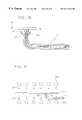
- FIG. 17is an explanatory diagram in connection with a substrate heating method according to the present invention.
- FIG. 18is a diagram showing the relationship between the lamp output ratio of the third evaluation sample and the measurement error.
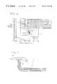
- FIG. 1a cross-sectional view of a temperature measuring apparatus 1 for a substrate is shown together with the substrate.
- the temperature measuring apparatus 1has such a structure wherein a thermocouple 11 is used as a temperature measuring means and the thermocouple 11 is covered with a covering member 21 .
- a voltmeter(not shown)is connected to the above-mentioned thermocouple 11 for measuring an electromotive force of the thermocouple 11 .
- thermocouple 11is made of, for example, platinum (Pt), platinum (Pt)0.10%rhodium (Rh) and a temperature measuring portion (alloy portion) 12 of the thermoe formed of an alloy of a platinum wire and platinum0.10%rhodium wire.
- an insulation tube 31is loosely inserted into at least either wire and the insulation tube 31 is made of, for example, quartz.
- the insulation tube 31is loosely inserted into a platinum conductor wire 13 .
- insulation tube 31may be loosely inserted into a platinum0.10%rhodium wire 14 .
- a first temperature measuring portion covering member 22is made of a material having high heat conductivity and in substantial contact with the temperature measuring portion 12 .
- the temperature measuring portion covering member 22is in substantial contact with the temperature measuring portion 12 and is made of silicon carbide, heat from substrate 51 sufficiently conducts to the temperature measuring portion 12 .
- the temperature measuring portion covering member 22has such a structure that its surface area is made small in order to restrain direct absorption of the light to the utmost and its heat capacity is made small to raise heat responsiveness. That is, the contour of the temperature measuring portion covering member 22 is shaped like a cap relative to the temperature measuring portion 12 and has dimensions of 1.4 mm in cap's outer diameter, 0.9 mm in cap's inner diameter and 1.4 mm in cap's height.
- a second temperature measuring portion covering member 23 of the above-mentioned covering member 21is.
- the quartzexcels in penetration property for infrared rays and is formed into a tube shape having a circular cross-section to substantially suppress the direct absorption of light.
- the substrate 51is horizontally supported by the temperature measuring portion covering member 22 , which is the foremost end portion of the above-mentioned temperature measuring apparatus 1 , together with plurality (for example, 2 pieces) of substrate supporting portions (diagrammatic showing is omitted) made of quartz, which project from a quartz tray (diagrammatic showing is omitted).
- thermocouple measuring means of the above-mentioned temperature measuring apparatus 1is covered with the covering member 21 , and of the covering member 21 , as the temperature measuring portion because covering member 22 in a portion covering the temperature measuring portion 12 of the thermocouple 11 is formed of a material having high heat conductive property, it becomes easy for the heat of the substrate 51 to conduct to the temperature measuring portion 12 . As a result, although measurement of the temperature through the temperature is measuring portion covering member 22 , it is effectively a measurement of the substrate temperature 51 .
- the wire portion covering member 23is made of quartz having a high light transmission factor, the wire portion covering member 23 absorbs essentially no light when it is subjected to light irradiation. As a result, because there is scarcely any rise in the temperature of wire portion covering member 23 due to light irradiation, any change in the measured value by the thermocouple 11 due to absorption of heat by the lined portion covering member 23 scarcely occurs.
- thermocouple 11each of surfaces of conductor wires 13 and 14 of thermocouple 11 are generally formed to easily reflect light. As a result, when thermocouple 11 is irradiated, it is rarely influenced by the irradiating light.
- the above-mentioned temperature measuring portion covering member 22is made of silicon carbide, which has a high thermal resistance and is thermally stable under a typical heating method temperature (below 12000 C.) for the normal substrate, the substrate 51 is never contaminated by portion covering member 22 at a time of the heating.
- a tube 112located inside a reaction furnace 111 , is a tube 112 , which is made of quartz glass having a high light transmission property for infrared rays, and a halogen lamp 113 for heating.
- the halogen lampsurrounds the outside periphery of the tube 112 .
- a door 115is installed which is opened or closed at a time when the substrate 51 is put in or pulled out and is fitted with packing 114 (for example, resinous packing) capable of making the inside of the tube 112 air tight when the inside of the above-mentioned tube 112 is sealed.
- a gas introducing tube 116is connected to the other end of the above-mentioned tube 112 to introduce gas thereinto.
- a tray 117 made of quartzfor supporting the substrate 51 .
- a substrate supporting portion 118 made of quartzOn the tray 117 is formed a substrate supporting portion 118 made of quartz.
- the substrate 51is also supported by the foremost end portion (that is, the temperature measuring portion 12 through the temperature measuring portion covering member 22 which was explained in the above-mentioned FIG. 1) of the temperature measuring apparatus 1 arranged on the tray 117 together with the substrate supporting portion 118 .
- the conductor wires 13 and 14 of the thermocouple 11 of the temperature measuring apparatus 1are led out through apertures 119 provided in an edge portion of the reaction furnace 111 .
- the light irradiation-type heating method apparatus 101is structured as mentioned above.
- Film thickness of each of the evaluation samplesare altered to change the emissivity of the substrate.
- a first evaluation sample 61is such that on one side (a front surface side) of a silicon substrate 62 are laminated an oxidized silicon film (SiO 2 ) 63 , a polycrystal silicon film 64 with a thickness of 150 nm and a capping oxidized silicon film 65 with a thickness of 300 nm, while on other side (rear surface side) of the silicon substrate 62 are laminated an oxidized silicon (SiO 2 ) film 66 and a polycrystal silicon film 67 with a thickness of 150 nm.
- the thicknesses of the above-mentioned oxidized silicon films 63 and 66are altered in a range of 700 nm-900 nm, but a light absorption quantity depends little on the film thickness.
- boron difluoride(BF2) is ion-implanted into the polycrystal silicon film 67 where the ion-implantation energy is 40 KeV and the dose amount is 5.4 ⁇ 10 14 /cm 2 .
- a second evaluation sample 71is such that on one side (front surface side) of a silicon substrate 72 are laminated an oxidized silicon (SiO 2 ) film 73 with a thickness of 800 nm, a polycrystal silicon film 74 with a thickness of 150 nm and a capping oxidized silicon film 75 with a thickness of 300 m, while on another side (rear surface side) of the substrate 72 are laminated an oxidized silicon (SiO 2 ) film 76 with a thickness of 800 nm and A polycrystal silicon film 77 .
- SiO 2oxidized silicon
- the thickness of the polycrystal silicon film 77 on the above-mentioned rear side 77are changed within a range of 150 nm to 350 nm with some variation in light absorption.
- boron difluoride(BF2) is ion-implanted into the polycrystal silicon film 74 on the front side where the ion-implantation energy is 40 KeV and the dose amount is 5.4 ⁇ 10 14 /cm 2 .
- a third evaluation sample 81is such that on one side (front surface side) of a silicon substrate 82 are laminated an oxidized silicon (SiO 2 ) film 83 , a polycrystal silicon film 84 with a thickness of 150 nm and a capping oxidized silicon film 85 with a thickness of 300 nm, while on the other side (rear surface side) of the substrate 82 are laminated an oxidized silicon film 86 and a polycrystal silicon film 87 with a thickness of 150 nm.
- SiO 2oxidized silicon
- Thicknesses of the oxidized silicon films 83 and 86are varied in a range of 100 nm-600 nm in steps of 100 nm, 200 nm, 300 nm, 400 nm and 600 nm. As a result, in the evaluation sample 81 , the amount of light absorption by the oxidized silicon films 83 and 86 depends a great deal on the thickness of the film.
- boron difluoride(BF2) is ion-implanted into the polycrystal silicon film 84 where the ion-implantation energy is 40 Kev and the dose amount is 5.4 ⁇ 10 14 /cm 2 .
- thermocouplesBy directly bonding thermocouples with heat resistance additives respectively to a plurality of the first evaluation samples 61 which have different film thicknesses of the oxidized silicon film 63 , to a plurality of the second evaluation samples 71 which have different film thicknesses of the polycrystal silicon film 77 and to a plurality of the third evaluation samples 81 which have different film thicknesses of the oxidized silicon films 83 and 86 , correct measurement of the temperatures using the thermocouples is carried out.
- the first evaluation sample 61 , the second evaluation sample 71 and the 3rd evaluation sample 81are substituted for the substrate 51 , and are subjected to heating by way of a Rapid Thermal Annealing (RTA) process using the light irradiation-type heating method apparatus 101 which is explained in the above-mentioned FIG. 2 .
- RTARapid Thermal Annealing
- Each evaluation sampleis put through a sequence of RTA steps is, as shown in FIG. 4 .
- Each evaluation sampleis placed in the tube 112 (refer to FIG. 2) wherein the temperature is set at 2000° C.
- the evaluation sampleis heated up to a set temperature T°C. at a heating speed of 100° C./Sec and the down to 4000 C at a cooling speed of 700 C/Sec. Thereafter, the evaluation sample is pulled out from inside of the tube 112 .
- the above-mentioned set temperatures T of the RTAare set at 900° C., 1000° C., 1050° C., 1100° C. and 1150° C.
- the following evaluation samplesare processed in the following manner: the identical lamp output is carried out on all of evaluation samples in which the thicknesses of the oxidized silicon films 63 and 66 of the evaluation sample 61 , the thickness of the polycrystal silicon film 77 of the second evaluation sample 71 and the thicknesses of the oxidized silicon films 83 and 86 of the third evaluation sample 81 are altered. That is, continuous heating is carried out by open loop control under the constant irradiation intensity of light.
- the temperatures of the respective evaluation samplesare measured by the temperature measuring apparatus 1 (refer to FIG. 1) of the present invention.
- the relationship between the measured values and the sheet resistancewill be explained with respect to FIG. 6 . Meanwhile, the measurement of the temperatures was carried out twice on the respective evaluation samples.
- results of the two times measurementsare shown together. Also, the ordinate shows the sheet resistance and the abscissa shows the substrate temperature measured by the temperature measuring apparatus 1 under the open loop control.
- the sheet resistance(the substrate temperature) changes depending on the differences in thicknesses of films formed on the substrates.
- the values of the sheet resistance (shown with white blank and black painted circles, triangles and square marks) versus temperatures measured by the temperature measuring apparatus 1 discussed in the above-mentioned FIG. 1,almost match the temperature versus sheet resistance curve C, which is the result of measuring temperature by directly bonding the thermocouple on the substrate, which was explained in FIG. 5 .
- the temperature measuring apparatus 1 of the present inventionis capable of carrying out accurate measurements of substrate temperatures with sufficient reproducibility on various substrates which have different substrate structures and different light absorption quantities.
- a temperature measuring apparatus 2is a comparative example in which the heat capacity and the surface area in the temperature measuring apparatus 1 , explained in the above-mentioned FIG. 1 are increased by using a, nearly ⁇ -lettered-type cross-sectional piece 26 or the temperature measuring portion covering member 22 of 1 covering the temperature measuring portion 12 . That is, what is provided is a collar around the periphery of the temperature measuring portion covering member 22 , as depicted in FIG. 1, which extends to and is in contact with the substrate 51 .
- temperatures of respective evaluation samplesare measured by the temperature measuring apparatus 2 which uses the temperature measuring portion covering member 26 .
- the resultswill be explained in connection with FIG. 8 .
- the sheet resistance(substrate temperature) changes depending on differences in thickness of films formed on the substrate.
- Heating at a set temperature of 1050° C. according to the sequence explained in connection with the above-mentioned FIG. 4is carried out on evaluation samples are altered in terms of the thicknesses of the oxidized silicon films 83 and 86 of the third evaluation sample.
- This heating methodis carried out under closed loop control and uses the temperature measuring apparatus 1 (refer to the above-mentioned FIG. 1 ), and the temperature measuring apparatus 2 (refer to the above-mentioned FIG. 7 ).
- the relationship between sheet resistance of respective evaluation samples and thicknesses of the oxidized silicon films at that timewill be shown in FIG. 9 .
- the relationship between the substrate temperatures and the thickness of the oxidized silicon films under the open loop controlwill be shown in FIG. 10 .
- the ordinateshows the sheet resistance and the abscissa shows the thickness of oxidized silicon film.
- the ordinateshows the substrate temperature and the abscissa shows the thickness of oxidized silicon film.
- black painted circle marksshow values under open loop control and white blank square marks show values under the closed loop control, using the temperature measuring apparatus 1 (refer to FIG. 1) and white blank triangle marks show values under closed loop control using the temperature measuring apparatus 2 (refer to FIG. 7 ).
- the lamp output on a front surface side as well as a rear-surface side of the substrateis identical.
- dependency of the sheet resistance (substrate temperature) on film thickness, under open loop controlis improved by using the temperature measuring apparatuses 1 and 2 .
- the above-mentioned temperature measuring apparatuses 1 and 2can accurately measure the temperature under open loop control, it does not lead to a complete solution of the dependency on film thickness when they are used for the measurement of the substrate temperature under closed loop control.
- temperature measuring apparatus 2With temperature measuring apparatus 2 , it is understood that there is less effect on the improvement of the dependency on the film thickness when compared with the use of temperature measuring apparatus 1 .
- explanationswill be made for this result.
- heating at a set temperature of 1050° C.was carried out according to the sequence explained in, connection with FIG. 4 with respect to the 3rd evaluation sample 81 ((3) of FIG. 3) wherein the thicknesses of the oxidized silicon films 83 and 86 are altered.
- the ordinateshows the ratio of the lamp output and the abscissa shows the thickness of the oxidized silicon film.
- the ordinateshows the ratio of the lamp output and the abscissa shows the substrate temperature converted from the sheet resistance.
- the ordinateshows the ratio of the lamp output and the abscissa shows the measured error which was obtained from the differences between the converted substrate temperatures and the measured temperatures by the temperature measuring apparatus 1 and 2 .
- black painted circle marksshow values under the open loop control
- white blank square marksshow values under the closed loop control using the temperature measuring apparatus 1
- white blank triangle marksshow values under the closed loop control using the temperature measuring apparatus 2 .
- the lamp output on the front surface side as well as the rear side of the substrateis identical.
- the lamp outputchanges in a linear form relative to the substrate temperature.
- the measured errors by the temperature measuring apparatuses 1 and 2become larger as the lamp output is increased, and this tendency becomes greater with the temperature measuring apparatus 2 than with the temperature measuring apparatus 1 , which proves that the temperature measuring apparatuses 1 and 2 directly absorb the light from the lamp. Therefore, there is a need for a structure to restrain the absorption of light to a minimum by reducing the surface area of the temperature measuring portion covering member 22 .
- thermocoupleis covered with silicon carbide and further, the contact area is enlarged to facilitate the heat conduction as in a conventional structure, substantial light is absorbed, thereby indicating an impossibility of carrying out precise measurements as under closed loop control.
- FIG. 11 to FIG. 13problematic points in relation to the measurement of the substrate temperatures by the temperature measuring apparatuses 1 and 2 are shown by using measured results of the third evaluation sample 81 [refer to (3) in FIG. 3 ] wherein the quantity of the light absorbed by the substrate changes greatly depending on the thickness of the oxidized silicon film.
- covering member 22covering the temperature measuring portion 12 , as small as possible and restrain the absorption of the light. This leads to, it is ascertained, the simultaneous lowering-of the heat capacity of the temperature measuring portion covering member 22 and improvement in heat responsiveness.
- the present inventionconstitutes the covering member 21 which includes the temperature measuring portion covering member 22 which has excellent heat conductivity and the lined portion covering member 23 which absorbs less radiation (in other words, excellent in light transmission factor).
- the covering memberis made up of one kind of material as in the conventional technology, it becomes possible, as mentioned above, to accurately measure the temperature of the substrate 51 (the evaluation samples 61 , 71 and 81 ).
- the temperature measuring portion covering member 22is made of silicon carbide, or another material having excellent heat conductivity. It may be possible that the temperature measuring portion covering member is made of, for example, aluminum nitride, silicide (for example, molybdenum silicide, titanium silicide, cobalt silicide, and the like) or alumina. For example, in a case of being made of alumina, because the reflection factor on the surface of the temperature measuring portion covering member 22 is high, the irradiated light for heating—the substrate 51 is reflected. For this reason, the temperature measuring portion covering member 22 is rarely heated by the irradiated light.
- silicidefor example, molybdenum silicide, titanium silicide, cobalt silicide, and the like
- the temperature measuring portion covering member 22As a result, the measuring errors due to the light absorption by the temperature measuring portion covering member 22 is restrained, thereby making it possible to carry out the measurement with high precision. Also, similar to the silicon carbide, the above-mentioned temperature measuring portion covering member 22 never contaminates the substrate 51 upon heat treatment.
- the wire portion covering member 23is made of quartz, but the second embodiment, (the wire portion covering member) is possibly made of a material which reflects the irradiated light heating the substrate 51 .
- the wire portion covering member 23is made of alumina.
- the wire portion covering member 23 for covering the conductor wires of the thermocouple 11reflects the light.
- silicidefor example, molybdenum silicide, titanium silicide, cobalt silicide, and the like
- aluminabecause the reflection factor on the surface of the temperature measuring portion covering member 22 is high, the irradiated light for heating the substrate 51 is reflected.
- the temperature measuring portion covering member 22is rarely heated by the irradiated light. As a result, the measuring errors due to the light absorption-by the temperature measuring portion covering member 22 is restrained, thereby making it possible to carry out the measurement with high precision. Also, similar to the silicon carbide, the above-mentioned temperature measuring portion covering member 22 does never contaminate the substrate 51 upon heat treatment.
- the problem of measuring errors caused by the light absorption when the substrate temperature is measuredcan be solved by using the temperature measuring apparatus 1 which was explained in the above-mentioned first embodiment.
- a temperature measuring apparatus for measuring the temperature while being in-contact with the substratelike the temperature measuring apparatus 1 , is the stability of the contact between the substrate and the temperature measuring portion of the temperature measuring apparatus. This means that because of a change in a contact area between the temperature measuring apparatus and the substrate due to a warp of the substrate, a surface state of the substrate and the like, a quantity of conducted heat from the substrate varies, resulting in the emergence of a deterioration in measuring accuracy.
- a temperature measuring apparatus 3has the same general structure as that of the temperature measuring apparatus 1 explained in the in connection with above mentioned FIG. 1, wherein a contact surface 22 A of the temperature measuring portion covering member 22 fixed on the temperature measuring portion 12 , which comes in contact with the substrate 51 , is formed into a convex curve surface.
- the temperature measuring apparatus 3 with a structure according to the above-mentioned 3rd embodimenthas the contact surface 22 A formed into the convex curve surface, the contact with the substrate 51 becomes a so-called point contact. For that reason, even if the contact surface of the substrate 51 is warped, its surface is uneven, or the contact surface 22 A comes in contact with the substrate 51 in a tilting state, the contact state of the point contact does not change. Therefore, it becomes possible to always maintain a constant state of contact (for example, a contact angle, a contact area and the like). As a result, because the measuring errors due to a contact state are reduced, stable measurement of the substrate temperature can be realized.
- a temperature measuring apparatus 4is such that a reflecting covering layer 41 for reflecting the light irradiated on the substrate 51 is formed on an outer periphery of the temperature measuring portion covering member 22 , fixed on the temperature measuring portion 12 , of the temperature measuring apparatus 1 .
- the temperature measuring apparatus 4has the reflecting covering layer 41 for reflecting the light irradiated on the substrate 51 , the layer being formed on the outer periphery of the temperature measuring portion covering member 22 , the light is not directly irradiated on the temperature measuring portion covering member 22 . As a result, the temperature measuring portion covering member 22 is not directly heated by the irradiated light, thereby making it possible to implement an improvement in the accuracy of measurement of the temperature of the substrate 51 .
- a temperature measuring apparatus 5is such that a light shielding plate 42 , for shielding the irradiated light, is formed on an optical path of the light irradiated on the temperature measuring portion covering member 22 and is fixed on the temperature measuring portion 12 of the temperature measuring apparatus 1 , as described in the above mentioned first embodiment, and is also near the temperature measuring portion covering member 22 .
- the above-mentioned light shielding plate 42is preferably made of material such as alumina, and the like which reflect light.
- the above-mentioned temperature measuring apparatus 5has the light shielding plate 42 formed near the above-mentioned temperature measuring portion covering member 22 for shielding the light irradiated on the rear side of the substrate 51 , the light is not directly irradiated on the temperature measuring portion covering member 22 .
- the temperature measuring portion covering member 22is not directly heated by the irradiated light, thereby making it possible to implement an improvement in of the accuracy of measurement of the temperature of the substrate 51 .
- a light irradiation type heating method device 101is installed with, for example, the temperature measuring apparatus 1 .
- the substrate 51 to be subjected to heat treatmentis inserted into the inside of the tube 112 of the light irradiation type heating method device 101 , and is supported by the tip portion (that is, the temperature measuring portion 12 through the temperature measuring portion covering member 22 explained in connection with the above-mentioned FIG. 1) of the temperature measuring apparatus 1 arranged on the tray 117 and by the substrate supporting portion 118 as well.
- the heating halogen lamp 113 provided around the periphery of the tube 112is made to emit light, and heating method of the substrate 51 is carried out by irradiating the light on the substrate 51 .
- the temperature of the substrate 51is measured by the above mentioned temperature measuring apparatus 1 .
- the temperature measuring apparatus 1in which the thermocouple 11 is covered with the covering member 21 , and of the covering member 22 , as the temperature measuring portion covering member 22 covering the temperature measuring portion 12 of the thermocouple 11 is made of a material having high heat conductivity, the temperature of the substrate 51 is measured, so that the temperature of the substrate 51 conducts to the temperature measuring portion 12 thanks to the temperature measuring portion covering member 22 being made of the high heat conductive material. For that reason, in spite of measuring the temperature through the covering member 21 , it becomes possible to accurately measure the temperature of the substrate 51 .
- the covering member in the other portion excluding the temperature measuring portion covering member 22that is, the wire portion covering member 23
- the wire portion covering member 23is made of a material having a high light transmission factor (or a material with a high light reflection factor)
- the wire portion covering member 23when subjected to the light irradiation in the midst of measuring, rarely absorbs light. For that reason, as an increase in the temperature of the wire covering member 23 due to the light irradiation becomes almost nothing, any change in the temperature measured values by the temperature measuring apparatus 1 due to heat absorption by the wire covering member 23 as well as any change in the temperature measured values due to radiation from the substrate 51 , seldom occur.
- the above mentioned temperature measuring apparatus 1it becomes possible for the above mentioned temperature measuring apparatus 1 to measure the temperature of the substrate 51 with high accuracy at a time of heat treatment.
- the temperature measuring apparatus 1was used, but by using other temperature measuring apparatus 2 to the temperature measuring apparatus 5 , it similarly becomes possible to measure the-temperature of the substrate 51 with high accuracy in the midst of the heating method.
- the irradiation intensity of light L1is irradiated on the front surface of the substrate 51 located opposite the rear surface of the substrate 51 i.e., on the side with which the temperature measuring portion 12 of the temperature measuring apparatus 1 for measuring the temperature of the substrate 51 comes in contact with the substrate.
- the light intensity of L1is relatively raised higher than the irradiation intensity of light L2, irradiated on the rear surface of the substrate 51 .
- the quantity of the irradiation light on the temperature measuring portion covering member 22can be reduced and hence, the improvement of the measuring accuracy of the temperature measuring apparatus 1 can be enhanced.
- the ratio between ratios of the lamp output compared with when the lamp output is 100% and the measured errors of the substrate temperatureswill be explained in connection with FIG. 18 .
- the ratio between the lamp output on the front surface side of the substrate and the lamp output on the rear surface side of the substrateis set to 2:1.
- the ordinateshows the ratios of the lamp output compared with when the lamp output is 100%
- the abscissashows the measured error which is obtained from the difference between the substrate conversion temperatures and the measured temperatures by the temperature measuring apparatus 1 .
- white blank triangle marksshow values under the closed loop control using the temperature measuring apparatus 1 .
- the measured error by the temperature measuring apparatus 1becomes larger as the lamp output is raised, but an increment thereof is small.
- the results shown in FIG. 18are from an experiment on a substrate of 5 inches in diameter, when compared with an experiment using a substrate of a large diameter such as 8 inches, the light irradiated from the lamp on the front surface side of the substrate tends to diffract to reach the rear surface side of the substrate. Therefore, the effects resulting from raising the, radiation intensity on the front surface side of the substrate do not appear so much.
- the measured errors by the temperature measuring apparatus 1which depend on the lamp output have been improved.
Landscapes
- Physics & Mathematics (AREA)
- Engineering & Computer Science (AREA)
- General Physics & Mathematics (AREA)
- Microelectronics & Electronic Packaging (AREA)
- Manufacturing & Machinery (AREA)
- Computer Hardware Design (AREA)
- Condensed Matter Physics & Semiconductors (AREA)
- Power Engineering (AREA)
- Health & Medical Sciences (AREA)
- Toxicology (AREA)
- High Energy & Nuclear Physics (AREA)
- Testing Or Measuring Of Semiconductors Or The Like (AREA)
- Measuring Temperature Or Quantity Of Heat (AREA)
- Investigating Or Analyzing Materials Using Thermal Means (AREA)
- Resistance Heating (AREA)
Abstract
Description
This invention relates to a substrate temperature measuring apparatus, a substrate temperature measuring method, a substrate heating method and a heating method apparatus.
In recent years, as semiconductor devices become minute, it becomes necessary to form shallow junctions with high precision, for MOS devices to restrain a short channel effect and for bipolar devices to improve their cutoff frequency fT. One method of forming a shallow junction is a heating method (RTA: Rapid Thermal Annealing) by light irradiation, which is capable of treating a device at a high temperature and for a short time, is employed. Also, the RTA is used for eliminating crystal defects which occur as a result of ion implantation, for various kinds of annealing such as a sinter and the like, and for forming an oxidized film and a nitrificated film. Therefore, it has become very important to accurately control a substrate temperature of a substrate having various film structures, a substrate having various impurity concentrations, and the like.
However, when the substrate heating method employs light irradiation, there are changes in emissivity of a substrate which are dependent on film structure, film quality, impurity concentration, and the like. This results in changes in the quantity of light absorbed (treatment temperature) by the substrate under circumstances where irradiation intensity is constant. Therefore, as a manufacturing process becomes more complex, it is very difficult to control the heated state of a substrate which contains, variations (dispersion of film thickness, film quality, the amount of impurity, structure and the like). Further, the temperature of the substrate changes depending on a change in the light transmission factor of the quartz tube which is employed as the heating apparatus, a change in a reflection factor of the inside wall of the chamber, and a change in the lamp output in terms of time and the like. In order to cope with this problem, closed loop control is under discussion which measures the substrate temperature and feeds back the measured value to control the lamp output is under discussion.
Also, one apparatus for measuring the substrate temperature, there is a radiation thermometer. This radiation thermometer has an advantage in that it can carry out the temperature measurement of the substrate without coming in contact therewith.
Another temperature measuring apparatus is a thermocouple. When the temperature measurement is carried out by a thermocouple, there are methods to get the thermocouple in direct contact with a surface of the substrate and to fix the thermocouple on the surface of the substrate by using a thermally stabilized adhesive, and so on. These methods have advantage in that when the temperature measuring portion (alloy portion) of the thermocouple comes in direct contact with the substrate it is possible to accurately measure the substrate temperature.
As for other temperature measuring apparatuses, an apparatus is disclosed in a Japanese patent application No 4148546 public bulletin, wherein the substrate temperature is indirectly measured by inserting the thermocouple into a covering member made of silicon carbide (SiC).
Temperature measurements made by using the above-mentioned radiation thermometer are different from the contact-type heat measuring method using thermocouples in that its measuring accuracy depends on the surface state of the object to be measured and hence, is strongly influenced by a measuring environment. With substrates having various film structures and impurity concentrations, there is different emissivity for every substrate. Accordingly, as there is a need to first obtain the emissivity of each substrate in order to carry out an accurate measurement.
Also, with the method for measuring substrate temperature by getting the thermocouple in direct contact with the substrate, problems occur with the deterioration in the thermocouple due to a reaction between the substrate and the thermocouple, metal contamination of the substrate, and the like.
Furthermore, with the method for measuring the temperature by inserting the thermocouple into the covering member, a problem of the metal contamination of the substrate by the thermoelectric couple is solved. However, the thermocouple is measuring the temperature of the covering member. Also, in a process wherein the substrate is subjected to heating by light irradiation heating apparatus, when the substrate temperature rises, the covering member is heated not only by thermal conduction, but by directly absorbing the irradiated light. As a result, the accurate measurement of the substrate temperature becomes difficult.
Also, the heat conduction from the substrate, absorption of radiation from the substrate by the covering member, and absorption of the irradiated lamp light differ depending on materials used for the covering member. Quartz and silicon carbide are shown as examples. When the quarts is used for the covering member, the light absorption can be restrained, but because the quartz has body heat conduction, the measurement of the substrate temperature is difficult and its thermal responsiveness deteriorates. On the other hand, when silicon carbide is used for the covering member, it excels in conducting substrate, heat but, because it absorbs a great deal of light, the measured temperature depends greatly on the light irradiation intensity. Due to these thermal characteristics, each of the materials has advantages as well as a drawback.
Another method to increase thermal conduction efficiency from the substrate employs machining the covering member flat at a contact portion between the covering member and the substrate , where two surfaces are in contact with each other, but this method leads to increasing the thermal capacity of the covering member. As a result, there is increased heating due to the direct absorption of light, thereby making it impossible to accurately measure the substrate temperature.
Where closed loop control is used to vary light irradiation intensity, the amount of heat absorbed by the covering changes depending on the irradiation intensity it is, therefore, impossible to accurately measure changes in the light absorption quantity (substrate temperature) due to changes in the irradiation factor of the substrate which has various kinds of film structures and impurity concentration. Furthermore, in the case of a sheath-type thermocouple, because a portion of the thermocouple, other than a point where the temperature is measured is heated, there is a concern that a high temperature region will occur in an middle region with respect to the “temperature measuring point”, thereby inviting a shunt error, which drops the accuracy of the measurement.
The present invention provides a substrate temperature measuring apparatus, a substrate temperature measuring method, a substrate heating method and a heating method apparatus with a view to solving the above-mentioned problems.
The substrate temperature measuring apparatus is equipped with a temperature measuring means and a covering member and the temperature measuring means measures the temperature of a substrate which is heated by light irradiation by contacting a temperature measuring portion of the temperature measuring means to the substrate through the covering member. A portion in the covering member that covers the measuring portion is made of a material having high heat conductivity. The other portion of the covering member which does not cover the measuring portion, consists of a material having high heat conductivity and is made of either a material having a high light transmittance factor or a material having a high light reflection factor.
In the above-mentioned temperature measuring apparatus, because the portion of the covering member covering the temperature measuring portion of the temperature measuring apparatus is made of a material with high heat conductivity, the substrate temperature tends to easily conduct to the temperature measuring portion. As a result, although it is a measurement of the temperature through the covering member, it becomes possible to measure the substrate temperature. Also, because the portion of the covering member not covering the measuring portion is made of a material having high heat conductivity with a high light transmission factor or material with the high reflection factor, the covering material covering the temperature measuring means never absorbs the light when subjected to the light irradiation in the midst of measuring. As a result, because there is scarcely any rise in the temperature of the covering member due to light irradiation, a change in a measured temperature value by the temperature measuring means due to the absorption of the covering member and a change in a measured temperature by radiation from the substrate almost never occurs.
A method for measuring the substrate temperature employs the above-described temperature measuring means and the covering member for covering it, for measuring the temperature of the substrate. The substrate is heated by light irradiation with the substrate temperature being measured by having the measuring portion of the temperature measuring means in contact with the substrate through the covering member.
Because the temperature of the substrate is measured by the covering member which is made of a material with a high heat conductivity, the temperature of the substrate is easily conducted to the heat-measuring unit by the covering member. As a result, although it is the measurement of the temperature of the covering member, it becomes possible to accurately measure the substrate temperature. Because a portion of the covering member is made of either a material having a high light transmittance factor or a material having a high light reflecting factor, the covering material almost never absorbs light when subjected to the light irradiation in the midst of measuring. As a result, because there is scarcely any rise in the temperature of the covering member due to the light irradiation, a change in a measured temperature value by the temperature measuring means due to heat absorption of the covering member and a change in a measured temperature by the radiation from the substrate almost never occurs.
A method for heating a substrate by way of light irradiation is a method wherein the light irradiation is conducted by raising an irradiation intensity of a light which is irradiated upon a substrate surface on the opposite side of a substrate from with which the temperature measuring portion of the temperature measuring apparatus for measuring the substrate temperature is in contact.
In the above-mentioned method for heating the substrate, the intensity of the light irradiated on the substrate surface on the side with which the temperature measuring portion is in contact is weakened, i.e., a quantity of the light irradiated on the temperature measuring portion becomes smaller. As a result, an effect on the temperature measuring portion by the light irradiation becomes less and measurement errors of the substrate temperature are reduced.
A heating method apparatus is equipped with a heating light source by way of the light irradiation, a member to be irradiated by the light from the heating light source, a temperature measuring portion for measuring the temperature of the heated member, a first temperature measuring portion covering member which is provided at one end of the temperature measuring portion and made of the material having high heat conductivity, and a second temperature measuring portion covering member which covers a periphery of the temperature measuring portion and is made of a material having a high light transmission factor.
In the above-mentioned heating method apparatus with covering members, as the first temperature measuring portion covering member for covering the temperature measuring portion is made of the material having high heat conductivity, the substrate temperature tends to easily conduct to the temperature measuring portion. For that reason, although it is the measurement of the temperature through the first temperature measuring portion covering member, it becomes possible to measure the substrate temperature. Also, because the second temperature measuring portion covering member is made of a material having high heat conductivity and with a high light transmission factor or a material with a high light reflection factor, when this portion is subjected to the light irradiation, it almost never absorbs the light. As a result, because there is scarcely any rise in the temperature of the covering member due to the light irradiation, a change in a measured temperature value by the temperature measuring means due to the absorption of the covering member and a change in a measured temperature by radiation from the substrate, almost never occurs.
FIG. 1 is a schematic structural cross-sectional diagram of a first embodiment of the invention in connection with a temperature measuring apparatus of the present invention;
FIG. 2 is a schematic structural cross-sectional diagram of one example of a light irradiation-type heating method apparatus using the temperature measuring apparatus;
FIG. 3 is a schematic structural cross-sectional diagram of each of evaluation samples;
FIG. 4 is an explanatory diagram of a sequence of RTA;
FIG. 5 is a diagram showing the relationship between a sheet resistance of the respective evaluation samples and a set temperature of the RTA;
FIG. 6 is a diagram showing the relationship between a measured temperature by the temperature measuring apparatus of the present invention and the sheet resistance;
FIG. 7 is a schematic structural cross-sectional diagram of the temperature measuring apparatus of a comparative example;
FIG. 8 is a diagram showing relations between the measured temperature by the temperature measuring apparatus of the comparative example and the sheet resistance;
FIG. 9 is a diagram showing the relationship between the sheet resistance of a third evaluation sample and a thickness of an oxidized silicon film;
FIG. 10 is a diagram showing the relationship between a substrate temperature of the third evaluation sample and the thickness of the oxidized silicon, film;
FIG. 11 is a diagram showing the relationship between a lamp output ratio of the third evaluation sample and the thickness of the oxidized silicon film;
FIG. 12 is a diagram showing the relationship between the lamp output ratio of the third evaluation sample and a substrate conversion temperature;
FIG. 13 is a diagram showing the relationship between the lamp output ratio of the third evaluation sample and a measurement error;
FIG. 14 is a schematic structural cross-sectional diagram of a third embodiment in connection with the temperature measuring apparatus;
FIG. 15 is a schematic structural cross-sectional diagram of a forth embodiment in connection with the temperature measuring apparatus;
FIG. 16 is a schematic structural cross-sectional diagram of a fifth embodiment in connection with the temperature measuring apparatus;
FIG. 17 is an explanatory diagram in connection with a substrate heating method according to the present invention; and
FIG. 18 is a diagram showing the relationship between the lamp output ratio of the third evaluation sample and the measurement error.
One example of a first embodiment of the present invention will be described with reference to the schematic structural cross-sectional block of FIG.1.
In FIG. 1, a cross-sectional view of atemperature measuring apparatus 1 for a substrate is shown together with the substrate.
Thetemperature measuring apparatus 1 has such a structure wherein a thermocouple11 is used as a temperature measuring means and the thermocouple11 is covered with a coveringmember 21. A voltmeter (not shown)is connected to the above-mentioned thermocouple11 for measuring an electromotive force of the thermocouple11.
The above-mentioned thermocouple11 is made of, for example, platinum (Pt), platinum (Pt)0.10%rhodium (Rh) and a temperature measuring portion (alloy portion)12 of the thermoe formed of an alloy of a platinum wire and platinum0.10%rhodium wire.
Also, aninsulation tube 31 is loosely inserted into at least either wire and theinsulation tube 31 is made of, for example, quartz. In this example, theinsulation tube 31 is loosely inserted into aplatinum conductor wire 13. Naturally, it may be possible thatinsulation tube 31 may be loosely inserted into a platinum0.10%rhodium wire 14.
Of the above-mentionedcovering member 21, a first temperature measuringportion covering member 22 is made of a material having high heat conductivity and in substantial contact with thetemperature measuring portion 12. This temperature measuringportion covering member 22 is made of, for example, a material which has about ten times the heat conductivity as that of quartz (heat conductivity=1.66.m-1.K-1), and preferably of a material having a heat conductivity more than 100W.m-1.K-1. One such material is silicon carbide (heat conductivty=261 W.m-1.k-1).
In this manner, because the temperature measuringportion covering member 22 is in substantial contact with thetemperature measuring portion 12 and is made of silicon carbide, heat fromsubstrate 51 sufficiently conducts to thetemperature measuring portion 12.
Further, the temperature measuringportion covering member 22 has such a structure that its surface area is made small in order to restrain direct absorption of the light to the utmost and its heat capacity is made small to raise heat responsiveness. That is, the contour of the temperature measuringportion covering member 22 is shaped like a cap relative to thetemperature measuring portion 12 and has dimensions of 1.4 mm in cap's outer diameter, 0.9 mm in cap's inner diameter and 1.4 mm in cap's height.
Also, a second temperature measuringportion covering member 23 of the above-mentionedcovering member 21 is. a wire portion covering member and is made of quartz. The quartz excels in penetration property for infrared rays and is formed into a tube shape having a circular cross-section to substantially suppress the direct absorption of light.
Thesubstrate 51 is horizontally supported by the temperature measuringportion covering member 22, which is the foremost end portion of the above-mentionedtemperature measuring apparatus 1, together with plurality (for example, 2 pieces) of substrate supporting portions (diagrammatic showing is omitted) made of quartz, which project from a quartz tray (diagrammatic showing is omitted).
The thermocouple measuring means of the above-mentionedtemperature measuring apparatus 1 is covered with the coveringmember 21, and of the coveringmember 21, as the temperature measuring portion because coveringmember 22 in a portion covering thetemperature measuring portion 12 of the thermocouple11 is formed of a material having high heat conductive property, it becomes easy for the heat of thesubstrate 51 to conduct to thetemperature measuring portion 12. As a result, although measurement of the temperature through the temperature is measuringportion covering member 22, it is effectively a measurement of thesubstrate temperature 51.
Also, as the wireportion covering member 23 is made of quartz having a high light transmission factor, the wireportion covering member 23 absorbs essentially no light when it is subjected to light irradiation. As a result, because there is scarcely any rise in the temperature of wireportion covering member 23 due to light irradiation, any change in the measured value by the thermocouple11 due to absorption of heat by the linedportion covering member 23 scarcely occurs.
Meanwhile, each of surfaces ofconductor wires
Furthermore, because the above-mentioned temperature measuringportion covering member 22 is made of silicon carbide, which has a high thermal resistance and is thermally stable under a typical heating method temperature (below 12000 C.) for the normal substrate, thesubstrate 51 is never contaminated byportion covering member 22 at a time of the heating.
One example of a light irradiation-type heating method apparatus using thetemperature measuring apparatus 1 will be described with reference to the schematic structural cross-sectional diagram in FIG.2.
As shown in FIG. 2, located inside areaction furnace 111, is atube 112, which is made of quartz glass having a high light transmission property for infrared rays, and ahalogen lamp 113 for heating. The halogen lamp surrounds the outside periphery of thetube 112. On one end of thereaction furnace 111 containing one end oftube 112, adoor 115 is installed which is opened or closed at a time when thesubstrate 51 is put in or pulled out and is fitted with packing114 (for example, resinous packing) capable of making the inside of thetube 112 air tight when the inside of the above-mentionedtube 112 is sealed.
Agas introducing tube 116 is connected to the other end of the above-mentionedtube 112 to introduce gas thereinto. Inside the above-mentionedtube 112 is placed atray 117 made of quartz for supporting thesubstrate 51. On thetray 117 is formed asubstrate supporting portion 118 made of quartz. Thesubstrate 51 is also supported by the foremost end portion (that is, thetemperature measuring portion 12 through the temperature measuringportion covering member 22 which was explained in the above-mentioned FIG. 1) of thetemperature measuring apparatus 1 arranged on thetray 117 together with thesubstrate supporting portion 118. Also, theconductor wires temperature measuring apparatus 1 are led out throughapertures 119 provided in an edge portion of thereaction furnace 111.
The light irradiation-typeheating method apparatus 101 is structured as mentioned above.
Structures of three kinds of the evaluation samples for measuring the substrate temperature will be described with reference to FIG.3. Film thickness of each of the evaluation samples are altered to change the emissivity of the substrate.
As shown in (1) of FIG. 3, afirst evaluation sample 61 is such that on one side (a front surface side) of asilicon substrate 62 are laminated an oxidized silicon film (SiO2)63, a polycrystal silicon film64 with a thickness of 150 nm and a capping oxidizedsilicon film 65 with a thickness of 300 nm, while on other side (rear surface side) of thesilicon substrate 62 are laminated an oxidized silicon (SiO2)film 66 and apolycrystal silicon film 67 with a thickness of 150 nm.
Then, the thicknesses of the above-mentionedoxidized silicon films
Also, boron difluoride (BF2) is ion-implanted into thepolycrystal silicon film 67 where the ion-implantation energy is 40 KeV and the dose amount is 5.4×10¹⁴/cm2.
As shown in (2) of FIG. 3, asecond evaluation sample 71 is such that on one side (front surface side) of asilicon substrate 72 are laminated an oxidized silicon (SiO2)film 73 with a thickness of 800 nm, apolycrystal silicon film 74 with a thickness of 150 nm and a capping oxidizedsilicon film 75 with a thickness of 300 m, while on another side (rear surface side) of thesubstrate 72 are laminated an oxidized silicon (SiO2)film 76 with a thickness of 800 nm and A polycrystal silicon film77.
Then, the thickness of the polycrystal silicon film77 on the above-mentioned rear side77 are changed within a range of 150 nm to 350 nm with some variation in light absorption.
Also, boron difluoride (BF2) is ion-implanted into thepolycrystal silicon film 74 on the front side where the ion-implantation energy is 40 KeV and the dose amount is 5.4×10¹⁴/cm2.
As shown in (3) of FIG. 3, athird evaluation sample 81 is such that on one side (front surface side) of asilicon substrate 82 are laminated an oxidized silicon (SiO2)film 83, apolycrystal silicon film 84 with a thickness of 150 nm and a capping oxidizedsilicon film 85 with a thickness of 300 nm, while on the other side (rear surface side) of thesubstrate 82 are laminated an oxidizedsilicon film 86 and apolycrystal silicon film 87 with a thickness of 150 nm.
Thicknesses of the oxidizedsilicon films evaluation sample 81, the amount of light absorption by the oxidizedsilicon films
Also, boron difluoride (BF2) is ion-implanted into thepolycrystal silicon film 84 where the ion-implantation energy is 40 Kev and the dose amount is 5.4×10¹⁴/cm2.
By directly bonding thermocouples with heat resistance additives respectively to a plurality of thefirst evaluation samples 61 which have different film thicknesses of the oxidizedsilicon film 63, to a plurality of thesecond evaluation samples 71 which have different film thicknesses of the polycrystal silicon film77 and to a plurality of thethird evaluation samples 81 which have different film thicknesses of the oxidizedsilicon films
In the measurement of the temperature, thefirst evaluation sample 61, thesecond evaluation sample 71 and the3rd evaluation sample 81 are substituted for thesubstrate 51, and are subjected to heating by way of a Rapid Thermal Annealing (RTA) process using the light irradiation-typeheating method apparatus 101 which is explained in the above-mentioned FIG.2. Each evaluation sample is put through a sequence of RTA steps is, as shown in FIG.4. Each evaluation sample is placed in the tube112 (refer to FIG. 2) wherein the temperature is set at 2000° C. Then, the evaluation sample is heated up to a set temperature T°C. at a heating speed of 100° C./Sec and the down to 4000 C at a cooling speed of 700 C/Sec. Thereafter, the evaluation sample is pulled out from inside of thetube 112.
The above-mentioned set temperatures T of the RTA are set at 900° C., 1000° C., 1050° C., 1100° C. and 1150° C.
The above-mentioned sequence of the RTA is just an example, and is capable of being changed according to circumstances.
The temperature dependency of the sheet resistance of each of the evaluation samples at each set temperature are shown in FIG. 5, where the ordinate shows the sheet resistance and the abscissa shows the-set temperature of the RTA.
As shown in FIG. 5, from 900° C. to about 950° C., a nearly constant sheet resistance of 2140 Ω/□ is shown, while when the temperature becomes higher than about 1000° C., the sheet resistance suddenly drops. Then, at 1050° C., the sheet resistance becomes about 1420 Ω/□, at 1100° C., it becomes about 980 Ω/□0 and at 1150° C, it becomes about 8000 Ω/□.
Nextly, in accordance with the above-mentioned sequence explained in FIG. 4, and using a lamp output where the substrate temperature becomes 1050° C. the following evaluation samples are processed in the following manner: the identical lamp output is carried out on all of evaluation samples in which the thicknesses of the oxidizedsilicon films evaluation sample 61, the thickness of the polycrystal silicon film77 of thesecond evaluation sample 71 and the thicknesses of the oxidizedsilicon films third evaluation sample 81 are altered. That is, continuous heating is carried out by open loop control under the constant irradiation intensity of light.
At that time, the temperatures of the respective evaluation samples are measured by the temperature measuring apparatus1 (refer to FIG. 1) of the present invention. Nextly, the relationship between the measured values and the sheet resistance will be explained with respect to FIG.6. Meanwhile, the measurement of the temperatures was carried out twice on the respective evaluation samples.
In FIG. 6, results of the two times measurements are shown together. Also, the ordinate shows the sheet resistance and the abscissa shows the substrate temperature measured by thetemperature measuring apparatus 1 under the open loop control.
As shown in FIG. 6, with open loop control heating carried out with the identical light irradiation intensity regardless of the substrates, the sheet resistance (the substrate temperature) changes depending on the differences in thicknesses of films formed on the substrates. The values of the sheet resistance (shown with white blank and black painted circles, triangles and square marks) versus temperatures measured by thetemperature measuring apparatus 1 discussed in the above-mentioned FIG. 1, almost match the temperature versus sheet resistance curve C, which is the result of measuring temperature by directly bonding the thermocouple on the substrate, which was explained in FIG.5.
From this, it can be said that thetemperature measuring apparatus 1 of the present invention is capable of carrying out accurate measurements of substrate temperatures with sufficient reproducibility on various substrates which have different substrate structures and different light absorption quantities.
Nextly, the influence of heat capacity and a surface (refer to FIG. 1) covering thetemperature measuring portion 12 of thetemperature measuring apparatus 1 on measured substrate temperatures was examined.
As shown in FIG. 7, atemperature measuring apparatus 2 is a comparative example in which the heat capacity and the surface area in thetemperature measuring apparatus 1, explained in the above-mentioned FIG. 1 are increased by using a, nearly Π-lettered-typecross-sectional piece 26 or the temperature measuringportion covering member 22 of 1 covering thetemperature measuring portion 12. That is, what is provided is a collar around the periphery of the temperature measuringportion covering member 22, as depicted in FIG. 1, which extends to and is in contact with thesubstrate 51.
In the same manner as explained in connection with the above-mentioned FIG. 6, temperatures of respective evaluation samples, as discussed in connection with FIG. 3, are measured by thetemperature measuring apparatus 2 which uses the temperature measuringportion covering member 26. The results will be explained in connection with FIG.8.
As shown in FIG. 8, where open loop control of heating is carried out with the identical light irradiation intensity regardless of the substrates, the sheet resistance (substrate temperature) changes depending on differences in thickness of films formed on the substrate. The values (shown by black painted circle, triangle, square marks) of the sheet resistance, for the substrates at the measured temperatures, is measured by the temperature measuring apparatus2 (refer to the above-mentioned FIG.7), almost match the temperature dependency curve versus sheet resistance depicted in FIG. 5 which is the result of measuring by directly bonding the thermocouple on the substrate.
From this fact, according to an evaluation of when the temperature measuring apparatus of the present invention is used for measuring the temperature under open loop control, wherein the light irradiation intensity is fixed, it is understood that satisfactory measurement of the temperature is possible irrespective of shapes (surface area, heat capacity, contact area with substrate and so on) of the temperature measuringportion covering member 22 covering thetemperature measuring portion 12.
Heating at a set temperature of 1050° C. according to the sequence explained in connection with the above-mentioned FIG. 4 is carried out on evaluation samples are altered in terms of the thicknesses of the oxidizedsilicon films
In FIG. 9, the ordinate shows the sheet resistance and the abscissa shows the thickness of oxidized silicon film.
In FIG. 10, the ordinate shows the substrate temperature and the abscissa shows the thickness of oxidized silicon film.
In these figures, black painted circle marks show values under open loop control and white blank square marks show values under the closed loop control, using the temperature measuring apparatus1 (refer to FIG. 1) and white blank triangle marks show values under closed loop control using the temperature measuring apparatus2 (refer to FIG.7).
The lamp output on a front surface side as well as a rear-surface side of the substrate is identical.
As shown in FIG.9 and FIG. 10, dependency of the sheet resistance (substrate temperature) on film thickness, under open loop control is improved by using thetemperature measuring apparatuses temperature measuring apparatuses temperature measuring apparatus 2, it is understood that there is less effect on the improvement of the dependency on the film thickness when compared with the use oftemperature measuring apparatus 1. Hereafter, explanations will be made for this result.
Under closed loop control using thetemperature measuring apparatuses silicon films
The relationship, at that time, between the ratios of the lamp output, when it is stabilized, and the thicknesses of the oxidizedsilicon films
Meanwhile, the above-mentioned ratios were determined when the lamp output was at 100%.
In FIG. 11, the ordinate shows the ratio of the lamp output and the abscissa shows the thickness of the oxidized silicon film. In FIG. 12, the ordinate shows the ratio of the lamp output and the abscissa shows the substrate temperature converted from the sheet resistance. Further, in FIG. 13, the ordinate shows the ratio of the lamp output and the abscissa shows the measured error which was obtained from the differences between the converted substrate temperatures and the measured temperatures by thetemperature measuring apparatus
In the figures, black painted circle marks show values under the open loop control, white blank square marks show values under the closed loop control using thetemperature measuring apparatus 1 and white blank triangle marks show values under the closed loop control using thetemperature measuring apparatus 2.
Further, in all cases, the lamp output on the front surface side as well as the rear side of the substrate is identical.
As shown in FIG. 11, under the closed loop control, it is understood that when thickness of the oxidized silicon film is such that the substrate temperature becomes lower, the substrate temperature is corrected by increasing the lamp output.
Also, as shown in FIG. 12, the lamp output changes in a linear form relative to the substrate temperature.
However, as shown in FIG. 13, the measured errors by thetemperature measuring apparatuses temperature measuring apparatus 2 than with thetemperature measuring apparatus 1, which proves that thetemperature measuring apparatuses portion covering member 22.
That is, with a structure in which the thermocouple is covered with silicon carbide and further, the contact area is enlarged to facilitate the heat conduction as in a conventional structure, substantial light is absorbed, thereby indicating an impossibility of carrying out precise measurements as under closed loop control.
In FIG. 11 to FIG. 13, problematic points in relation to the measurement of the substrate temperatures by thetemperature measuring apparatuses
However, in a practically managed manufacturing process of a semiconductor device, fluctuation in the light absorption (substrate temperature) due to dispersion with variations of film thickness and film quality is far smaller than the above-mentioned set film thickness condition of oxidized silicon film. Therefore, it is possible to adequately solve the dependency of the sheet resistance (substrate temperature) on film thickness, under open loop control, by closed loop control which uses thetemperature measuring apparatus 1.
As set forth, in order to carry out highly precise measurement under close loop control, it is necessary to make coveringmember 22, covering thetemperature measuring portion 12, as small as possible and restrain the absorption of the light. This leads to, it is ascertained, the simultaneous lowering-of the heat capacity of the temperature measuringportion covering member 22 and improvement in heat responsiveness.
In this manner, the present invention constitutes the coveringmember 21 which includes the temperature measuringportion covering member 22 which has excellent heat conductivity and the linedportion covering member 23 which absorbs less radiation (in other words, excellent in light transmission factor). Hence, unlike the temperature measuring apparatus wherein the covering member is made up of one kind of material as in the conventional technology, it becomes possible, as mentioned above, to accurately measure the temperature of the substrate51 (theevaluation samples
With the above-mentionedtemperature measuring apparatus 1, the temperature measuringportion covering member 22 is made of silicon carbide, or another material having excellent heat conductivity. It may be possible that the temperature measuring portion covering member is made of, for example, aluminum nitride, silicide (for example, molybdenum silicide, titanium silicide, cobalt silicide, and the like) or alumina. For example, in a case of being made of alumina, because the reflection factor on the surface of the temperature measuringportion covering member 22 is high, the irradiated light for heating—thesubstrate 51 is reflected. For this reason, the temperature measuringportion covering member 22 is rarely heated by the irradiated light. As a result, the measuring errors due to the light absorption by the temperature measuringportion covering member 22 is restrained, thereby making it possible to carry out the measurement with high precision. Also, similar to the silicon carbide, the above-mentioned temperature measuringportion covering member 22 never contaminates thesubstrate 51 upon heat treatment.
In the above-mentioned first embodiment, the wireportion covering member 23 is made of quartz, but the second embodiment, (the wire portion covering member) is possibly made of a material which reflects the irradiated light heating thesubstrate 51. For example, the wireportion covering member 23 is made of alumina.
In a structure like this, when subjected to the light irradiation, the wireportion covering member 23 for covering the conductor wires of the thermocouple11 reflects the light. As a result, because there is scarcely any rise in the temperature of the linedportion covering member 23 due to the light irradiation, almost no change in the value of the measured temperature of the thermocouple11 due to aluminum nitride, silicide (for example, molybdenum silicide, titanium silicide, cobalt silicide, and the like) or alumina. For example, in a case of being made of alumina, because the reflection factor on the surface of the temperature measuringportion covering member 22 is high, the irradiated light for heating thesubstrate 51 is reflected. For this reason, the temperature measuringportion covering member 22 is rarely heated by the irradiated light. As a result, the measuring errors due to the light absorption-by the temperature measuringportion covering member 22 is restrained, thereby making it possible to carry out the measurement with high precision. Also, similar to the silicon carbide, the above-mentioned temperature measuringportion covering member 22 does never contaminate thesubstrate 51 upon heat treatment.
The problem of measuring errors caused by the light absorption when the substrate temperature is measured can be solved by using thetemperature measuring apparatus 1 which was explained in the above-mentioned first embodiment. However, what is posed as a problem for a temperature measuring apparatus for measuring the temperature while being in-contact with the substrate, like thetemperature measuring apparatus 1, is the stability of the contact between the substrate and the temperature measuring portion of the temperature measuring apparatus. This means that because of a change in a contact area between the temperature measuring apparatus and the substrate due to a warp of the substrate, a surface state of the substrate and the like, a quantity of conducted heat from the substrate varies, resulting in the emergence of a deterioration in measuring accuracy. Specifically, in a case where the contact surface is made flat in order to make a contact area wider, because of a slipping off of a contact angle due to a mere warp of the substrate, unevenness of the surface and the like, the contact area varies widely. A temperature measuring apparatus for improving reproducibility of this contact state will be explained with a schematic structural cross-sectional diagram in FIG. 14 as a third embodiment.
As shown in FIG. 14, atemperature measuring apparatus 3 has the same general structure as that of thetemperature measuring apparatus 1 explained in the in connection with above mentioned FIG. 1, wherein acontact surface 22A of the temperature measuringportion covering member 22 fixed on thetemperature measuring portion 12, which comes in contact with thesubstrate 51, is formed into a convex curve surface.
As thetemperature measuring apparatus 3 with a structure according to the above-mentioned 3rd embodiment has thecontact surface 22A formed into the convex curve surface, the contact with thesubstrate 51 becomes a so-called point contact. For that reason, even if the contact surface of thesubstrate 51 is warped, its surface is uneven, or thecontact surface 22A comes in contact with thesubstrate 51 in a tilting state, the contact state of the point contact does not change. Therefore, it becomes possible to always maintain a constant state of contact (for example, a contact angle, a contact area and the like). As a result, because the measuring errors due to a contact state are reduced, stable measurement of the substrate temperature can be realized.
Nextly, a fourth embodiment will be explained with reference to a schematic cross-sectional view of FIG.15.
As shown in FIG. 15, atemperature measuring apparatus 4 is such that a reflectingcovering layer 41 for reflecting the light irradiated on thesubstrate 51 is formed on an outer periphery of the temperature measuringportion covering member 22, fixed on thetemperature measuring portion 12, of thetemperature measuring apparatus 1.
Because the above-mentionedtemperature measuring apparatus 4 has the reflectingcovering layer 41 for reflecting the light irradiated on thesubstrate 51, the layer being formed on the outer periphery of the temperature measuringportion covering member 22, the light is not directly irradiated on the temperature measuringportion covering member 22. As a result, the temperature measuringportion covering member 22 is not directly heated by the irradiated light, thereby making it possible to implement an improvement in the accuracy of measurement of the temperature of thesubstrate 51.
Nextly, a fifth embodiment will be explained with reference to a schematic cross-sectional view of FIG.16.
As shown in FIG. 16, atemperature measuring apparatus 5 is such that alight shielding plate 42, for shielding the irradiated light, is formed on an optical path of the light irradiated on the temperature measuringportion covering member 22 and is fixed on thetemperature measuring portion 12 of thetemperature measuring apparatus 1, as described in the above mentioned first embodiment, and is also near the temperature measuringportion covering member 22.
The above-mentionedlight shielding plate 42 is preferably made of material such as alumina, and the like which reflect light.
As the above-mentionedtemperature measuring apparatus 5 has thelight shielding plate 42 formed near the above-mentioned temperature measuringportion covering member 22 for shielding the light irradiated on the rear side of thesubstrate 51, the light is not directly irradiated on the temperature measuringportion covering member 22. As a result, the temperature measuringportion covering member 22 is not directly heated by the irradiated light, thereby making it possible to implement an improvement in of the accuracy of measurement of the temperature of thesubstrate 51.
Nextly, examples of methods for measuring the substrate temperature by using any of the above-mentionedtemperature measuring apparatus 1 through5, explained as follows.
Like the one explained in connection with FIG. 2, for example, a light irradiation typeheating method device 101 is installed with, for example, thetemperature measuring apparatus 1. First of all, thesubstrate 51 to be subjected to heat treatment is inserted into the inside of thetube 112 of the light irradiation typeheating method device 101, and is supported by the tip portion (that is, thetemperature measuring portion 12 through the temperature measuringportion covering member 22 explained in connection with the above-mentioned FIG. 1) of thetemperature measuring apparatus 1 arranged on thetray 117 and by thesubstrate supporting portion 118 as well. Then, theheating halogen lamp 113 provided around the periphery of thetube 112 is made to emit light, and heating method of thesubstrate 51 is carried out by irradiating the light on thesubstrate 51. At this time, the temperature of thesubstrate 51 is measured by the above mentionedtemperature measuring apparatus 1.
According to the above-mentioned method for measuring the temperature of the substrate, by using thetemperature measuring apparatus 1 in which the thermocouple11 is covered with the coveringmember 21, and of the coveringmember 22, as the temperature measuringportion covering member 22 covering thetemperature measuring portion 12 of the thermocouple11 is made of a material having high heat conductivity, the temperature of thesubstrate 51 is measured, so that the temperature of thesubstrate 51 conducts to thetemperature measuring portion 12 thanks to the temperature measuringportion covering member 22 being made of the high heat conductive material. For that reason, in spite of measuring the temperature through the coveringmember 21, it becomes possible to accurately measure the temperature of thesubstrate 51. Also, because the covering member in the other portion excluding the temperature measuringportion covering member 22, that is, the wireportion covering member 23, is made of a material having a high light transmission factor (or a material with a high light reflection factor), the wireportion covering member 23, when subjected to the light irradiation in the midst of measuring, rarely absorbs light. For that reason, as an increase in the temperature of thewire covering member 23 due to the light irradiation becomes almost nothing, any change in the temperature measured values by thetemperature measuring apparatus 1 due to heat absorption by thewire covering member 23 as well as any change in the temperature measured values due to radiation from thesubstrate 51, seldom occur.
Therefore, it becomes possible for the above mentionedtemperature measuring apparatus 1 to measure the temperature of thesubstrate 51 with high accuracy at a time of heat treatment.
In the above-mentioned explanation, thetemperature measuring apparatus 1 was used, but by using othertemperature measuring apparatus 2 to thetemperature measuring apparatus 5, it similarly becomes possible to measure the-temperature of thesubstrate 51 with high accuracy in the midst of the heating method.
Nextly, one example of a heating method for the substrate, carrying out high precision measurements of the temperature by reducing the quantity of light irradiation on the temperature measuring apparatus, will be explained with reference to FIG.17.
The irradiation intensity of light L1 is irradiated on the front surface of thesubstrate 51 located opposite the rear surface of thesubstrate 51 i.e., on the side with which thetemperature measuring portion 12 of thetemperature measuring apparatus 1 for measuring the temperature of thesubstrate 51 comes in contact with the substrate. The light intensity of L1 is relatively raised higher than the irradiation intensity of light L2, irradiated on the rear surface of thesubstrate 51.
That is, by raising the radiation intensity of alamp 113A on the front surface side of thesubstrate 51 higher relative to the radiation intensity of alamp 113B on the rear surface side of thesubstrate 51, the quantity of the irradiation light on the temperature measuringportion covering member 22 can be reduced and hence, the improvement of the measuring accuracy of thetemperature measuring apparatus 1 can be enhanced.
Nextly, as an example, the relationship between ratios of the lamp output compared with when the lamp output is 100% and the measured errors of the substrate temperatures will be explained in connection with FIG.18. Meanwhile, the ratio between the lamp output on the front surface side of the substrate and the lamp output on the rear surface side of the substrate is set to 2:1.
In FIG. 18, the ordinate shows the ratios of the lamp output compared with when the lamp output is 100%, and the abscissa shows the measured error which is obtained from the difference between the substrate conversion temperatures and the measured temperatures by thetemperature measuring apparatus 1. In the figure, white blank triangle marks show values under the closed loop control using thetemperature measuring apparatus 1.
As shown in FIG. 18, the measured error by thetemperature measuring apparatus 1 becomes larger as the lamp output is raised, but an increment thereof is small. As the results shown in FIG. 18 are from an experiment on a substrate of 5 inches in diameter, when compared with an experiment using a substrate of a large diameter such as 8 inches, the light irradiated from the lamp on the front surface side of the substrate tends to diffract to reach the rear surface side of the substrate. Therefore, the effects resulting from raising the, radiation intensity on the front surface side of the substrate do not appear so much. However, compared with the time when the ratio of the lamp output was 1:1 as shown in the above-mentioned FIG. 13, it is understood that the measured errors by thetemperature measuring apparatus 1, which depend on the lamp output have been improved. This proves that the quantity of light from the lamp, that thetemperature measuring apparatus 1 directly absorbs, is reduced. Therefore, it is understood that measurements with high accuracy can be carried out by reducing the light intensity irradiated on the surface of the substrate on the side where the temperature measuring apparatus is provided.
Claims (28)
1. In a temperature measuring apparatus for a substrate provided with a temperature measuring means and a covering member for covering said temperature measuring means in which a temperature measuring portion of said temperature measuring means is made to be in contact with a substrate through said covering member to measure a temperature of said substrate heated by irradiation of light,
the temperature measuring apparatus for a substrate being characterized in that
said covering member having a portion covering said temperature measuring portion, said portion being made of a material with a high heat conductivity, and
said covering member another portion, excluding the covering member which is made of said material with a high heat conductivity, said another portion being made of a material with a high light transmission factor.
2. In a temperature measuring apparatus for a substrate provided with a temperature measuring means and a covering member for covering said temperature measuring means in which a temperature measuring portion of said temperature measuring means is made to be in contact with a substrate through said covering member to measure a temperature of said substrate heated by irradiation of light,
the temperature measuring apparatus for a substrate being characterized in that
said covering member, having a portion covering said temperature measuring portion, said portion being made of a material with a high heat conductivity, and
said covering member, having another portion, excluding the covering member which is made of said material with a high heat conductivity, said another portion being made of a material with a high light reflection factor.
3. A temperature measuring apparatus for a substrate as claimed in claim1, being characterized in that
a surface of said covering member which comes in contact with said substrate is formed into a convex curve surface.
4. A temperature measuring apparatus for a substrate as claimed in claim2, being characterized in that
a surface of said covering member which comes in contact with said substrate is formed into a convex curve surface.
5. A temperature measuring apparatus for a substrate as claimed in claim1, being characterized in that
said covering member made of the material with a high heat conductivity is made of silicon carbide, aluminum nitride, silicide or alumina.
6. A temperature measuring apparatus for a substrate as claimed in claim2, being characterized in that
said covering member made of the material with a high heat conductivity is made of silicon carbide, aluminum nitride, silicide or alumina.
7. A temperature measuring apparatus for a substrate as claimed in claim1, being characterized in that
on an outer periphery of said covering member made of the material with a high heat conductivity, a reflecting covering layer made of a material with a high reflection factor relative to said light is formed.
8. A temperature measuring apparatus for a substrate as claimed in claim2, being characterized in that
on an outer periphery of said covering member made of the material with a high heat conductivity, a reflecting covering layer made of a material with a high reflection factor relative to said light is formed.
9. A temperature measuring apparatus for a substrate as claimed in claim1, being characterized in that
on an optical path of said light irradiated on the covering member made of said material with a high heat conductivity and near the covering member made of said material with a high heat conductivity, a light shielding plate for shielding said light is provided.
10. A temperature measuring apparatus for a substrate as claimed in claim2, being characterized in that
on an optical path of said light irradiated on the covering member made of said material with a high heat conductivity and near the covering member made of said material with a high heat conductivity, a light shielding plate for shielding said light is provided.
11. In a temperature measuring method for a substrate provided with a temperature measuring means and a covering member for covering said temperature measuring means in which a temperature measuring portion of said temperature measuring means is made to be in contact with a substrate through said covering member to measure a temperature of said substrate heated by irradiation of light,
the temperature measuring method for a substrate being characterized in that a temperature of said substrate is measured by using a temperature measuring apparatus which
said covering member, having a portion covering said temperature measuring portion, said portion being made of a material with a high heat conductivity, and
said covering member, having another portion, excluding the covering member which is made of said material with a high heat conductivity, said another portion being made of a material with a high light reflection factor.
12. In a temperature measuring method for a substrate provided with a temperature measuring means and a covering member for covering said temperature measuring means in which a temperature measuring portion of said temperature measuring means is made to be in contact with a substrate through said covering member to measure a temperature of said substrate heated by irradiation of light,
the temperature measuring method for a substrate being characterized in that a temperature of said substrate is measured by using a temperature measuring apparatus which
said covering member, having a portion covering said temperature measuring portion, said another portion being made of a material with a high heat conductivity, and
said covering member, having another portion, excluding the covering member which is made of said material with a high heat conductivity, said another portion being made of a material with a high light transmission factor.
13. A heating method for heating a substrate by irradiation of light,
the heating method being characterized in that the
irradiation of a light irradiated on a surface of the substrate on an opposite side from a surface of said substrate to which a temperature measuring portion of a temperature measuring apparatus for measuring a temperature of said substrate comes in contact, is raised higher than the irradiation intensity of a light irradiated on the surface of the substrate on the side with which said temperature measuring portion comes in contact.
14. A heating method apparatus being for a member, being characterized by comprising;
a heating light source for heating by way of irradiation of light;
a member to be heated irradiated by the light from said heating light source;
a temperature heating portion for measuring a temperature of said member to be heated;
a first temperature measuring portion covering member which is provided at one end of said temperature measuring portion and made of a material with a high heat conductivity; and
a second temperature measuring portion covering member covering a periphery of said temperature measuring portion and made of a material with a high light transmission factor.
15. A heating method for a member, being characterized by comprising:
a heating light source for heating by way of irradiation of light;
a member to be irradiated by the light from said heating light source;
a temperature measuring portion for measuring a temperature of said member to be heated;
a first temperature measuring portion covering member which is provided at one end of said temperature measuring portion and made of a material with a high heat conductivity; and
a second temperature measuring portion covering member covering a periphery of said temperature measuring portion and made of a material with a high light reflection factor.
16. A heating method apparatus for the member as claimed in claim14, being characterized in that
said first temperature measuring portion covering member is made to be in contact with said member to be heated for measuring a temperature thereof.
17. A heating method apparatus for a member as claimed in claim15, being characterized in that
said first temperature measuring portion covering member is made to be in contact with said member to be heated for measuring a temperature thereof.
18. A heating method apparatus for a member as claimed in claim16, being characterized in that
said member to be heated is a semiconductor substrate.
19. A heating method apparatus for a member as claimed in claim17, being characterized in that
said member to be heated is a semiconductor substrate.
20. A heating method apparatus for a member as claimed in claim16, being characterized in that
a surface of said first temperature measuring portion covering member which comes in contact with said member to be heated is formed into a convex curve surface.
21. A heating method apparatus for a member as claimed in claim17, being characterized in that
a surface of said first temperature measuring portion covering member which comes in contact with said member to be heated is formed into a convex curve surface.
22. A temperature measuring device for measuring the temperature of an irradiated substrate:
said temperature measuring device having sensor means responsive to temperature and non-sensor means, said sensor means being connected to said non-sensor means;
said temperature measuring device also having covering means for covering said sensor means and said non-sensor means;
said covering means having a high heat conductivity first portion covering said sensor means and substantially coextensive therewith and a high light transmission factor second portion covering said non-sensor means and substantially coextensive therewith; and,
said temperature measuring device having further means for directly contacting said substrate.
23. The temperature measuring device of claim22 wherein said further means for directly contacting said substrate includes said sensor means and said high heat conductivity first portion of said covering means, said sensor means contacting said substrate through said covering means first portion.
24. The temperature measuring device of claim23 wherein said covering means first portion has a convex curve shape where it contacts said substrate.
25. The temperature measuring device of claim23 wherein said covering means first portion further includes radiation reflecting means.
26. The temperature measuring device of claim23 wherein said covering means further includes light shielding means connected to, and extending away from, said covering means.
27. The temperature measuring apparatus of claim1 wherein said covering member portion covering said temperature measuring portion is made of a material with higher heat conductivity and a lesser light transmission factor than the material of said another portion.
28. The temperature measuring apparatus of claim2 wherein said covering member portion covering said temperature measuring portion is made of a material with higher heat conductivity and a lesser light reflection factor than the material of said another portion.
Applications Claiming Priority (3)
| Application Number | Priority Date | Filing Date | Title |
|---|---|---|---|
| JP9043166AJPH10239165A (en) | 1997-02-27 | 1997-02-27 | Method and apparatus for measuring temperature of substrate, and heating method for substrate |
| JP9-043166 | 1997-02-27 | ||
| PCT/JP1998/000779WO1998038673A1 (en) | 1997-02-27 | 1998-02-26 | Substrate temperature measuring instrument, method of measuring substrate temperature, substrate heating method and heat treatment device |
Publications (1)
| Publication Number | Publication Date |
|---|---|
| US6311016B1true US6311016B1 (en) | 2001-10-30 |
Family
ID=12656303
Family Applications (1)
| Application Number | Title | Priority Date | Filing Date |
|---|---|---|---|
| US09/171,786Expired - Fee RelatedUS6311016B1 (en) | 1997-02-27 | 1998-02-26 | Substrate temperature measuring apparatus, substrate temperature measuring method, substrate heating method and heat treatment apparatus |
Country Status (6)
| Country | Link |
|---|---|
| US (1) | US6311016B1 (en) |
| JP (1) | JPH10239165A (en) |
| KR (3) | KR20000064976A (en) |
| DE (1) | DE19880398B4 (en) |
| TW (1) | TW362149B (en) |
| WO (1) | WO1998038673A1 (en) |
Cited By (364)
| Publication number | Priority date | Publication date | Assignee | Title |
|---|---|---|---|---|
| US6464393B2 (en)* | 1999-12-03 | 2002-10-15 | Sumitomo Electric Industries, Ltd. | Surface temperature sensor head |
| US6515261B1 (en)* | 2002-03-06 | 2003-02-04 | Applied Materials, Inc. | Enhanced lift pin |
| WO2003044477A1 (en)* | 2001-11-20 | 2003-05-30 | Citizen Watch Co., Ltd. | Thermometer |
| US20030178405A1 (en)* | 2002-03-15 | 2003-09-25 | Mcwilliams Kevin Ronald | Electrical heating assembly |
| WO2003083422A1 (en)* | 2002-03-29 | 2003-10-09 | Axcelis Technologies, Inc. | Contact temperature probe and process |
| US20060289795A1 (en)* | 2005-06-02 | 2006-12-28 | Dubois Dale R | Vacuum reaction chamber with x-lamp heater |
| US20080317093A1 (en)* | 2005-04-12 | 2008-12-25 | Gert Mau | Sensor Arrangement for Temperature Measurement |
| US20090052498A1 (en)* | 2007-08-24 | 2009-02-26 | Asm America, Inc. | Thermocouple |
| US20100286842A1 (en)* | 2009-05-06 | 2010-11-11 | Asm America, Inc. | Smart Temperature Measuring Device |
| US20130148693A1 (en)* | 2009-05-06 | 2013-06-13 | Asm America, Inc. | Thermocouple assembly with guarded thermocouple junction |
| US10229833B2 (en) | 2016-11-01 | 2019-03-12 | Asm Ip Holding B.V. | Methods for forming a transition metal nitride film on a substrate by atomic layer deposition and related semiconductor device structures |
| US10249577B2 (en) | 2016-05-17 | 2019-04-02 | Asm Ip Holding B.V. | Method of forming metal interconnection and method of fabricating semiconductor apparatus using the method |
| US10249524B2 (en) | 2017-08-09 | 2019-04-02 | Asm Ip Holding B.V. | Cassette holder assembly for a substrate cassette and holding member for use in such assembly |
| US10262859B2 (en) | 2016-03-24 | 2019-04-16 | Asm Ip Holding B.V. | Process for forming a film on a substrate using multi-port injection assemblies |
| US10269558B2 (en) | 2016-12-22 | 2019-04-23 | Asm Ip Holding B.V. | Method of forming a structure on a substrate |
| US10276355B2 (en) | 2015-03-12 | 2019-04-30 | Asm Ip Holding B.V. | Multi-zone reactor, system including the reactor, and method of using the same |
| US10283353B2 (en) | 2017-03-29 | 2019-05-07 | Asm Ip Holding B.V. | Method of reforming insulating film deposited on substrate with recess pattern |
| US10290508B1 (en) | 2017-12-05 | 2019-05-14 | Asm Ip Holding B.V. | Method for forming vertical spacers for spacer-defined patterning |
| US10312055B2 (en) | 2017-07-26 | 2019-06-04 | Asm Ip Holding B.V. | Method of depositing film by PEALD using negative bias |
| US10312129B2 (en) | 2015-09-29 | 2019-06-04 | Asm Ip Holding B.V. | Variable adjustment for precise matching of multiple chamber cavity housings |
| US10319588B2 (en) | 2017-10-10 | 2019-06-11 | Asm Ip Holding B.V. | Method for depositing a metal chalcogenide on a substrate by cyclical deposition |
| US10322384B2 (en) | 2015-11-09 | 2019-06-18 | Asm Ip Holding B.V. | Counter flow mixer for process chamber |
| US10340135B2 (en) | 2016-11-28 | 2019-07-02 | Asm Ip Holding B.V. | Method of topologically restricted plasma-enhanced cyclic deposition of silicon or metal nitride |
| US10340125B2 (en) | 2013-03-08 | 2019-07-02 | Asm Ip Holding B.V. | Pulsed remote plasma method and system |
| US10343920B2 (en) | 2016-03-18 | 2019-07-09 | Asm Ip Holding B.V. | Aligned carbon nanotubes |
| US10361201B2 (en) | 2013-09-27 | 2019-07-23 | Asm Ip Holding B.V. | Semiconductor structure and device formed using selective epitaxial process |
| US10366864B2 (en) | 2013-03-08 | 2019-07-30 | Asm Ip Holding B.V. | Method and system for in-situ formation of intermediate reactive species |
| US10364493B2 (en) | 2016-08-25 | 2019-07-30 | Asm Ip Holding B.V. | Exhaust apparatus and substrate processing apparatus having an exhaust line with a first ring having at least one hole on a lateral side thereof placed in the exhaust line |
| US10367080B2 (en) | 2016-05-02 | 2019-07-30 | Asm Ip Holding B.V. | Method of forming a germanium oxynitride film |
| US10364496B2 (en) | 2011-06-27 | 2019-07-30 | Asm Ip Holding B.V. | Dual section module having shared and unshared mass flow controllers |
| US10381226B2 (en) | 2016-07-27 | 2019-08-13 | Asm Ip Holding B.V. | Method of processing substrate |
| US10381219B1 (en) | 2018-10-25 | 2019-08-13 | Asm Ip Holding B.V. | Methods for forming a silicon nitride film |
| US10378106B2 (en) | 2008-11-14 | 2019-08-13 | Asm Ip Holding B.V. | Method of forming insulation film by modified PEALD |
| US10388509B2 (en) | 2016-06-28 | 2019-08-20 | Asm Ip Holding B.V. | Formation of epitaxial layers via dislocation filtering |
| US10388513B1 (en) | 2018-07-03 | 2019-08-20 | Asm Ip Holding B.V. | Method for depositing silicon-free carbon-containing film as gap-fill layer by pulse plasma-assisted deposition |
| US10395919B2 (en) | 2016-07-28 | 2019-08-27 | Asm Ip Holding B.V. | Method and apparatus for filling a gap |
| US10403504B2 (en) | 2017-10-05 | 2019-09-03 | Asm Ip Holding B.V. | Method for selectively depositing a metallic film on a substrate |
| US10410943B2 (en) | 2016-10-13 | 2019-09-10 | Asm Ip Holding B.V. | Method for passivating a surface of a semiconductor and related systems |
| US10435790B2 (en) | 2016-11-01 | 2019-10-08 | Asm Ip Holding B.V. | Method of subatmospheric plasma-enhanced ALD using capacitively coupled electrodes with narrow gap |
| US10438965B2 (en) | 2014-12-22 | 2019-10-08 | Asm Ip Holding B.V. | Semiconductor device and manufacturing method thereof |
| US10446393B2 (en) | 2017-05-08 | 2019-10-15 | Asm Ip Holding B.V. | Methods for forming silicon-containing epitaxial layers and related semiconductor device structures |
| US10458018B2 (en) | 2015-06-26 | 2019-10-29 | Asm Ip Holding B.V. | Structures including metal carbide material, devices including the structures, and methods of forming same |
| US10468262B2 (en) | 2017-02-15 | 2019-11-05 | Asm Ip Holding B.V. | Methods for forming a metallic film on a substrate by a cyclical deposition and related semiconductor device structures |
| US10468251B2 (en) | 2016-02-19 | 2019-11-05 | Asm Ip Holding B.V. | Method for forming spacers using silicon nitride film for spacer-defined multiple patterning |
| US10480072B2 (en) | 2009-04-06 | 2019-11-19 | Asm Ip Holding B.V. | Semiconductor processing reactor and components thereof |
| US10483099B1 (en) | 2018-07-26 | 2019-11-19 | Asm Ip Holding B.V. | Method for forming thermally stable organosilicon polymer film |
| US10501866B2 (en) | 2016-03-09 | 2019-12-10 | Asm Ip Holding B.V. | Gas distribution apparatus for improved film uniformity in an epitaxial system |
| US10504742B2 (en) | 2017-05-31 | 2019-12-10 | Asm Ip Holding B.V. | Method of atomic layer etching using hydrogen plasma |
| US10510536B2 (en) | 2018-03-29 | 2019-12-17 | Asm Ip Holding B.V. | Method of depositing a co-doped polysilicon film on a surface of a substrate within a reaction chamber |
| US10529563B2 (en) | 2017-03-29 | 2020-01-07 | Asm Ip Holdings B.V. | Method for forming doped metal oxide films on a substrate by cyclical deposition and related semiconductor device structures |
| US10529542B2 (en) | 2015-03-11 | 2020-01-07 | Asm Ip Holdings B.V. | Cross-flow reactor and method |
| US10529554B2 (en) | 2016-02-19 | 2020-01-07 | Asm Ip Holding B.V. | Method for forming silicon nitride film selectively on sidewalls or flat surfaces of trenches |
| US10535516B2 (en) | 2018-02-01 | 2020-01-14 | Asm Ip Holdings B.V. | Method for depositing a semiconductor structure on a surface of a substrate and related semiconductor structures |
| US10541333B2 (en) | 2017-07-19 | 2020-01-21 | Asm Ip Holding B.V. | Method for depositing a group IV semiconductor and related semiconductor device structures |
| US10541173B2 (en) | 2016-07-08 | 2020-01-21 | Asm Ip Holding B.V. | Selective deposition method to form air gaps |
| US10559458B1 (en) | 2018-11-26 | 2020-02-11 | Asm Ip Holding B.V. | Method of forming oxynitride film |
| US10566223B2 (en) | 2012-08-28 | 2020-02-18 | Asm Ip Holdings B.V. | Systems and methods for dynamic semiconductor process scheduling |
| US10561975B2 (en) | 2014-10-07 | 2020-02-18 | Asm Ip Holdings B.V. | Variable conductance gas distribution apparatus and method |
| US10590535B2 (en) | 2017-07-26 | 2020-03-17 | Asm Ip Holdings B.V. | Chemical treatment, deposition and/or infiltration apparatus and method for using the same |
| US10600661B2 (en)* | 2015-05-20 | 2020-03-24 | Ultech Co., Ltd. | Rapid heat treatment apparatus |
| US10600673B2 (en) | 2015-07-07 | 2020-03-24 | Asm Ip Holding B.V. | Magnetic susceptor to baseplate seal |
| US10605530B2 (en) | 2017-07-26 | 2020-03-31 | Asm Ip Holding B.V. | Assembly of a liner and a flange for a vertical furnace as well as the liner and the vertical furnace |
| US10604847B2 (en) | 2014-03-18 | 2020-03-31 | Asm Ip Holding B.V. | Gas distribution system, reactor including the system, and methods of using the same |
| US10607895B2 (en) | 2017-09-18 | 2020-03-31 | Asm Ip Holdings B.V. | Method for forming a semiconductor device structure comprising a gate fill metal |
| USD880437S1 (en) | 2018-02-01 | 2020-04-07 | Asm Ip Holding B.V. | Gas supply plate for semiconductor manufacturing apparatus |
| US10612137B2 (en) | 2016-07-08 | 2020-04-07 | Asm Ip Holdings B.V. | Organic reactants for atomic layer deposition |
| US10612136B2 (en) | 2018-06-29 | 2020-04-07 | ASM IP Holding, B.V. | Temperature-controlled flange and reactor system including same |
| US10622375B2 (en) | 2016-11-07 | 2020-04-14 | Asm Ip Holding B.V. | Method of processing a substrate and a device manufactured by using the method |
| US10643904B2 (en) | 2016-11-01 | 2020-05-05 | Asm Ip Holdings B.V. | Methods for forming a semiconductor device and related semiconductor device structures |
| US10643826B2 (en) | 2016-10-26 | 2020-05-05 | Asm Ip Holdings B.V. | Methods for thermally calibrating reaction chambers |
| US10658205B2 (en) | 2017-09-28 | 2020-05-19 | Asm Ip Holdings B.V. | Chemical dispensing apparatus and methods for dispensing a chemical to a reaction chamber |
| US10658181B2 (en) | 2018-02-20 | 2020-05-19 | Asm Ip Holding B.V. | Method of spacer-defined direct patterning in semiconductor fabrication |
| US10655221B2 (en) | 2017-02-09 | 2020-05-19 | Asm Ip Holding B.V. | Method for depositing oxide film by thermal ALD and PEALD |
| US10665452B2 (en) | 2016-05-02 | 2020-05-26 | Asm Ip Holdings B.V. | Source/drain performance through conformal solid state doping |
| US10685834B2 (en) | 2017-07-05 | 2020-06-16 | Asm Ip Holdings B.V. | Methods for forming a silicon germanium tin layer and related semiconductor device structures |
| US10683571B2 (en) | 2014-02-25 | 2020-06-16 | Asm Ip Holding B.V. | Gas supply manifold and method of supplying gases to chamber using same |
| US10692741B2 (en) | 2017-08-08 | 2020-06-23 | Asm Ip Holdings B.V. | Radiation shield |
| US10707106B2 (en) | 2011-06-06 | 2020-07-07 | Asm Ip Holding B.V. | High-throughput semiconductor-processing apparatus equipped with multiple dual-chamber modules |
| US20200219739A1 (en)* | 2019-01-08 | 2020-07-09 | Nissin Ion Equipment Co., Ltd. | Substrate temperature measurement device and an apparatus having substrate temperature measurement device |
| US10714315B2 (en) | 2012-10-12 | 2020-07-14 | Asm Ip Holdings B.V. | Semiconductor reaction chamber showerhead |
| US10714335B2 (en) | 2017-04-25 | 2020-07-14 | Asm Ip Holding B.V. | Method of depositing thin film and method of manufacturing semiconductor device |
| US10714385B2 (en) | 2016-07-19 | 2020-07-14 | Asm Ip Holding B.V. | Selective deposition of tungsten |
| US10714350B2 (en) | 2016-11-01 | 2020-07-14 | ASM IP Holdings, B.V. | Methods for forming a transition metal niobium nitride film on a substrate by atomic layer deposition and related semiconductor device structures |
| US10734244B2 (en) | 2017-11-16 | 2020-08-04 | Asm Ip Holding B.V. | Method of processing a substrate and a device manufactured by the same |
| US10734497B2 (en) | 2017-07-18 | 2020-08-04 | Asm Ip Holding B.V. | Methods for forming a semiconductor device structure and related semiconductor device structures |
| US10731249B2 (en) | 2018-02-15 | 2020-08-04 | Asm Ip Holding B.V. | Method of forming a transition metal containing film on a substrate by a cyclical deposition process, a method for supplying a transition metal halide compound to a reaction chamber, and related vapor deposition apparatus |
| US10741385B2 (en) | 2016-07-28 | 2020-08-11 | Asm Ip Holding B.V. | Method and apparatus for filling a gap |
| US10755922B2 (en) | 2018-07-03 | 2020-08-25 | Asm Ip Holding B.V. | Method for depositing silicon-free carbon-containing film as gap-fill layer by pulse plasma-assisted deposition |
| US10770336B2 (en) | 2017-08-08 | 2020-09-08 | Asm Ip Holding B.V. | Substrate lift mechanism and reactor including same |
| US10770286B2 (en) | 2017-05-08 | 2020-09-08 | Asm Ip Holdings B.V. | Methods for selectively forming a silicon nitride film on a substrate and related semiconductor device structures |
| US10767789B2 (en) | 2018-07-16 | 2020-09-08 | Asm Ip Holding B.V. | Diaphragm valves, valve components, and methods for forming valve components |
| US10787741B2 (en) | 2014-08-21 | 2020-09-29 | Asm Ip Holding B.V. | Method and system for in situ formation of gas-phase compounds |
| US10797133B2 (en) | 2018-06-21 | 2020-10-06 | Asm Ip Holding B.V. | Method for depositing a phosphorus doped silicon arsenide film and related semiconductor device structures |
| US10804098B2 (en) | 2009-08-14 | 2020-10-13 | Asm Ip Holding B.V. | Systems and methods for thin-film deposition of metal oxides using excited nitrogen-oxygen species |
| US10811256B2 (en) | 2018-10-16 | 2020-10-20 | Asm Ip Holding B.V. | Method for etching a carbon-containing feature |
| USD900036S1 (en) | 2017-08-24 | 2020-10-27 | Asm Ip Holding B.V. | Heater electrical connector and adapter |
| US10818758B2 (en) | 2018-11-16 | 2020-10-27 | Asm Ip Holding B.V. | Methods for forming a metal silicate film on a substrate in a reaction chamber and related semiconductor device structures |
| US10832903B2 (en) | 2011-10-28 | 2020-11-10 | Asm Ip Holding B.V. | Process feed management for semiconductor substrate processing |
| US10829852B2 (en) | 2018-08-16 | 2020-11-10 | Asm Ip Holding B.V. | Gas distribution device for a wafer processing apparatus |
| US10847365B2 (en) | 2018-10-11 | 2020-11-24 | Asm Ip Holding B.V. | Method of forming conformal silicon carbide film by cyclic CVD |
| US10847371B2 (en) | 2018-03-27 | 2020-11-24 | Asm Ip Holding B.V. | Method of forming an electrode on a substrate and a semiconductor device structure including an electrode |
| US10847366B2 (en) | 2018-11-16 | 2020-11-24 | Asm Ip Holding B.V. | Methods for depositing a transition metal chalcogenide film on a substrate by a cyclical deposition process |
| US10844484B2 (en) | 2017-09-22 | 2020-11-24 | Asm Ip Holding B.V. | Apparatus for dispensing a vapor phase reactant to a reaction chamber and related methods |
| US10854498B2 (en) | 2011-07-15 | 2020-12-01 | Asm Ip Holding B.V. | Wafer-supporting device and method for producing same |
| US10851456B2 (en) | 2016-04-21 | 2020-12-01 | Asm Ip Holding B.V. | Deposition of metal borides |
| USD903477S1 (en) | 2018-01-24 | 2020-12-01 | Asm Ip Holdings B.V. | Metal clamp |
| US10858737B2 (en) | 2014-07-28 | 2020-12-08 | Asm Ip Holding B.V. | Showerhead assembly and components thereof |
| US10865475B2 (en) | 2016-04-21 | 2020-12-15 | Asm Ip Holding B.V. | Deposition of metal borides and silicides |
| US10867786B2 (en) | 2018-03-30 | 2020-12-15 | Asm Ip Holding B.V. | Substrate processing method |
| US10867788B2 (en) | 2016-12-28 | 2020-12-15 | Asm Ip Holding B.V. | Method of forming a structure on a substrate |
| US10872771B2 (en) | 2018-01-16 | 2020-12-22 | Asm Ip Holding B. V. | Method for depositing a material film on a substrate within a reaction chamber by a cyclical deposition process and related device structures |
| US10883175B2 (en) | 2018-08-09 | 2021-01-05 | Asm Ip Holding B.V. | Vertical furnace for processing substrates and a liner for use therein |
| US10886123B2 (en) | 2017-06-02 | 2021-01-05 | Asm Ip Holding B.V. | Methods for forming low temperature semiconductor layers and related semiconductor device structures |
| US10892156B2 (en) | 2017-05-08 | 2021-01-12 | Asm Ip Holding B.V. | Methods for forming a silicon nitride film on a substrate and related semiconductor device structures |
| US10896820B2 (en) | 2018-02-14 | 2021-01-19 | Asm Ip Holding B.V. | Method for depositing a ruthenium-containing film on a substrate by a cyclical deposition process |
| US10910262B2 (en) | 2017-11-16 | 2021-02-02 | Asm Ip Holding B.V. | Method of selectively depositing a capping layer structure on a semiconductor device structure |
| US10914004B2 (en) | 2018-06-29 | 2021-02-09 | Asm Ip Holding B.V. | Thin-film deposition method and manufacturing method of semiconductor device |
| US10923344B2 (en) | 2017-10-30 | 2021-02-16 | Asm Ip Holding B.V. | Methods for forming a semiconductor structure and related semiconductor structures |
| US10928731B2 (en) | 2017-09-21 | 2021-02-23 | Asm Ip Holding B.V. | Method of sequential infiltration synthesis treatment of infiltrateable material and structures and devices formed using same |
| US10934619B2 (en) | 2016-11-15 | 2021-03-02 | Asm Ip Holding B.V. | Gas supply unit and substrate processing apparatus including the gas supply unit |
| US10941490B2 (en) | 2014-10-07 | 2021-03-09 | Asm Ip Holding B.V. | Multiple temperature range susceptor, assembly, reactor and system including the susceptor, and methods of using the same |
| US10975470B2 (en) | 2018-02-23 | 2021-04-13 | Asm Ip Holding B.V. | Apparatus for detecting or monitoring for a chemical precursor in a high temperature environment |
| US11001925B2 (en) | 2016-12-19 | 2021-05-11 | Asm Ip Holding B.V. | Substrate processing apparatus |
| US11018002B2 (en) | 2017-07-19 | 2021-05-25 | Asm Ip Holding B.V. | Method for selectively depositing a Group IV semiconductor and related semiconductor device structures |
| US11015245B2 (en) | 2014-03-19 | 2021-05-25 | Asm Ip Holding B.V. | Gas-phase reactor and system having exhaust plenum and components thereof |
| US11018047B2 (en) | 2018-01-25 | 2021-05-25 | Asm Ip Holding B.V. | Hybrid lift pin |
| US11022879B2 (en) | 2017-11-24 | 2021-06-01 | Asm Ip Holding B.V. | Method of forming an enhanced unexposed photoresist layer |
| US11024523B2 (en) | 2018-09-11 | 2021-06-01 | Asm Ip Holding B.V. | Substrate processing apparatus and method |
| US11031242B2 (en) | 2018-11-07 | 2021-06-08 | Asm Ip Holding B.V. | Methods for depositing a boron doped silicon germanium film |
| USD922229S1 (en) | 2019-06-05 | 2021-06-15 | Asm Ip Holding B.V. | Device for controlling a temperature of a gas supply unit |
| US11049751B2 (en) | 2018-09-14 | 2021-06-29 | Asm Ip Holding B.V. | Cassette supply system to store and handle cassettes and processing apparatus equipped therewith |
| US11056567B2 (en) | 2018-05-11 | 2021-07-06 | Asm Ip Holding B.V. | Method of forming a doped metal carbide film on a substrate and related semiconductor device structures |
| US11053591B2 (en) | 2018-08-06 | 2021-07-06 | Asm Ip Holding B.V. | Multi-port gas injection system and reactor system including same |
| US11056344B2 (en) | 2017-08-30 | 2021-07-06 | Asm Ip Holding B.V. | Layer forming method |
| US11069510B2 (en) | 2017-08-30 | 2021-07-20 | Asm Ip Holding B.V. | Substrate processing apparatus |
| US11081345B2 (en) | 2018-02-06 | 2021-08-03 | Asm Ip Holding B.V. | Method of post-deposition treatment for silicon oxide film |
| US11088002B2 (en) | 2018-03-29 | 2021-08-10 | Asm Ip Holding B.V. | Substrate rack and a substrate processing system and method |
| US11087997B2 (en) | 2018-10-31 | 2021-08-10 | Asm Ip Holding B.V. | Substrate processing apparatus for processing substrates |
| US11114283B2 (en) | 2018-03-16 | 2021-09-07 | Asm Ip Holding B.V. | Reactor, system including the reactor, and methods of manufacturing and using same |
| US11114294B2 (en) | 2019-03-08 | 2021-09-07 | Asm Ip Holding B.V. | Structure including SiOC layer and method of forming same |
| USD930782S1 (en) | 2019-08-22 | 2021-09-14 | Asm Ip Holding B.V. | Gas distributor |
| US11127617B2 (en) | 2017-11-27 | 2021-09-21 | Asm Ip Holding B.V. | Storage device for storing wafer cassettes for use with a batch furnace |
| US11127589B2 (en) | 2019-02-01 | 2021-09-21 | Asm Ip Holding B.V. | Method of topology-selective film formation of silicon oxide |
| USD931978S1 (en) | 2019-06-27 | 2021-09-28 | Asm Ip Holding B.V. | Showerhead vacuum transport |
| US11139308B2 (en) | 2015-12-29 | 2021-10-05 | Asm Ip Holding B.V. | Atomic layer deposition of III-V compounds to form V-NAND devices |
| US11139191B2 (en) | 2017-08-09 | 2021-10-05 | Asm Ip Holding B.V. | Storage apparatus for storing cassettes for substrates and processing apparatus equipped therewith |
| US11158513B2 (en) | 2018-12-13 | 2021-10-26 | Asm Ip Holding B.V. | Methods for forming a rhenium-containing film on a substrate by a cyclical deposition process and related semiconductor device structures |
| US11171025B2 (en) | 2019-01-22 | 2021-11-09 | Asm Ip Holding B.V. | Substrate processing device |
| USD935572S1 (en) | 2019-05-24 | 2021-11-09 | Asm Ip Holding B.V. | Gas channel plate |
| US11205585B2 (en) | 2016-07-28 | 2021-12-21 | Asm Ip Holding B.V. | Substrate processing apparatus and method of operating the same |
| US11217444B2 (en) | 2018-11-30 | 2022-01-04 | Asm Ip Holding B.V. | Method for forming an ultraviolet radiation responsive metal oxide-containing film |
| US11222772B2 (en) | 2016-12-14 | 2022-01-11 | Asm Ip Holding B.V. | Substrate processing apparatus |
| USD940837S1 (en) | 2019-08-22 | 2022-01-11 | Asm Ip Holding B.V. | Electrode |
| US11227789B2 (en) | 2019-02-20 | 2022-01-18 | Asm Ip Holding B.V. | Method and apparatus for filling a recess formed within a substrate surface |
| US11227782B2 (en) | 2019-07-31 | 2022-01-18 | Asm Ip Holding B.V. | Vertical batch furnace assembly |
| US11232963B2 (en) | 2018-10-03 | 2022-01-25 | Asm Ip Holding B.V. | Substrate processing apparatus and method |
| US11233133B2 (en) | 2015-10-21 | 2022-01-25 | Asm Ip Holding B.V. | NbMC layers |
| US11230766B2 (en) | 2018-03-29 | 2022-01-25 | Asm Ip Holding B.V. | Substrate processing apparatus and method |
| US11251040B2 (en) | 2019-02-20 | 2022-02-15 | Asm Ip Holding B.V. | Cyclical deposition method including treatment step and apparatus for same |
| US11251068B2 (en) | 2018-10-19 | 2022-02-15 | Asm Ip Holding B.V. | Substrate processing apparatus and substrate processing method |
| USD944946S1 (en) | 2019-06-14 | 2022-03-01 | Asm Ip Holding B.V. | Shower plate |
| US11270899B2 (en) | 2018-06-04 | 2022-03-08 | Asm Ip Holding B.V. | Wafer handling chamber with moisture reduction |
| US11274369B2 (en) | 2018-09-11 | 2022-03-15 | Asm Ip Holding B.V. | Thin film deposition method |
| US11282698B2 (en) | 2019-07-19 | 2022-03-22 | Asm Ip Holding B.V. | Method of forming topology-controlled amorphous carbon polymer film |
| US11289326B2 (en) | 2019-05-07 | 2022-03-29 | Asm Ip Holding B.V. | Method for reforming amorphous carbon polymer film |
| US11286558B2 (en) | 2019-08-23 | 2022-03-29 | Asm Ip Holding B.V. | Methods for depositing a molybdenum nitride film on a surface of a substrate by a cyclical deposition process and related semiconductor device structures including a molybdenum nitride film |
| US11286562B2 (en) | 2018-06-08 | 2022-03-29 | Asm Ip Holding B.V. | Gas-phase chemical reactor and method of using same |
| US11295980B2 (en) | 2017-08-30 | 2022-04-05 | Asm Ip Holding B.V. | Methods for depositing a molybdenum metal film over a dielectric surface of a substrate by a cyclical deposition process and related semiconductor device structures |
| USD947913S1 (en) | 2019-05-17 | 2022-04-05 | Asm Ip Holding B.V. | Susceptor shaft |
| USD948463S1 (en) | 2018-10-24 | 2022-04-12 | Asm Ip Holding B.V. | Susceptor for semiconductor substrate supporting apparatus |
| USD949319S1 (en) | 2019-08-22 | 2022-04-19 | Asm Ip Holding B.V. | Exhaust duct |
| US11306395B2 (en) | 2017-06-28 | 2022-04-19 | Asm Ip Holding B.V. | Methods for depositing a transition metal nitride film on a substrate by atomic layer deposition and related deposition apparatus |
| US11315794B2 (en) | 2019-10-21 | 2022-04-26 | Asm Ip Holding B.V. | Apparatus and methods for selectively etching films |
| US11339476B2 (en) | 2019-10-08 | 2022-05-24 | Asm Ip Holding B.V. | Substrate processing device having connection plates, substrate processing method |
| US11342216B2 (en) | 2019-02-20 | 2022-05-24 | Asm Ip Holding B.V. | Cyclical deposition method and apparatus for filling a recess formed within a substrate surface |
| US11345999B2 (en) | 2019-06-06 | 2022-05-31 | Asm Ip Holding B.V. | Method of using a gas-phase reactor system including analyzing exhausted gas |
| US11355338B2 (en) | 2019-05-10 | 2022-06-07 | Asm Ip Holding B.V. | Method of depositing material onto a surface and structure formed according to the method |
| US11361990B2 (en) | 2018-05-28 | 2022-06-14 | Asm Ip Holding B.V. | Substrate processing method and device manufactured by using the same |
| US11374112B2 (en) | 2017-07-19 | 2022-06-28 | Asm Ip Holding B.V. | Method for depositing a group IV semiconductor and related semiconductor device structures |
| US11378337B2 (en) | 2019-03-28 | 2022-07-05 | Asm Ip Holding B.V. | Door opener and substrate processing apparatus provided therewith |
| US11390946B2 (en) | 2019-01-17 | 2022-07-19 | Asm Ip Holding B.V. | Methods of forming a transition metal containing film on a substrate by a cyclical deposition process |
| US11393690B2 (en) | 2018-01-19 | 2022-07-19 | Asm Ip Holding B.V. | Deposition method |
| US11390945B2 (en) | 2019-07-03 | 2022-07-19 | Asm Ip Holding B.V. | Temperature control assembly for substrate processing apparatus and method of using same |
| US11401605B2 (en) | 2019-11-26 | 2022-08-02 | Asm Ip Holding B.V. | Substrate processing apparatus |
| US11414760B2 (en) | 2018-10-08 | 2022-08-16 | Asm Ip Holding B.V. | Substrate support unit, thin film deposition apparatus including the same, and substrate processing apparatus including the same |
| US11424119B2 (en) | 2019-03-08 | 2022-08-23 | Asm Ip Holding B.V. | Method for selective deposition of silicon nitride layer and structure including selectively-deposited silicon nitride layer |
| US11430674B2 (en) | 2018-08-22 | 2022-08-30 | Asm Ip Holding B.V. | Sensor array, apparatus for dispensing a vapor phase reactant to a reaction chamber and related methods |
| US11430640B2 (en) | 2019-07-30 | 2022-08-30 | Asm Ip Holding B.V. | Substrate processing apparatus |
| US11437241B2 (en) | 2020-04-08 | 2022-09-06 | Asm Ip Holding B.V. | Apparatus and methods for selectively etching silicon oxide films |
| US11443926B2 (en) | 2019-07-30 | 2022-09-13 | Asm Ip Holding B.V. | Substrate processing apparatus |
| US11447861B2 (en) | 2016-12-15 | 2022-09-20 | Asm Ip Holding B.V. | Sequential infiltration synthesis apparatus and a method of forming a patterned structure |
| US11447864B2 (en) | 2019-04-19 | 2022-09-20 | Asm Ip Holding B.V. | Layer forming method and apparatus |
| USD965044S1 (en) | 2019-08-19 | 2022-09-27 | Asm Ip Holding B.V. | Susceptor shaft |
| US11453943B2 (en) | 2016-05-25 | 2022-09-27 | Asm Ip Holding B.V. | Method for forming carbon-containing silicon/metal oxide or nitride film by ALD using silicon precursor and hydrocarbon precursor |
| USD965524S1 (en) | 2019-08-19 | 2022-10-04 | Asm Ip Holding B.V. | Susceptor support |
| US11469098B2 (en) | 2018-05-08 | 2022-10-11 | Asm Ip Holding B.V. | Methods for depositing an oxide film on a substrate by a cyclical deposition process and related device structures |
| US11476109B2 (en) | 2019-06-11 | 2022-10-18 | Asm Ip Holding B.V. | Method of forming an electronic structure using reforming gas, system for performing the method, and structure formed using the method |
| US11473195B2 (en) | 2018-03-01 | 2022-10-18 | Asm Ip Holding B.V. | Semiconductor processing apparatus and a method for processing a substrate |
| US11482412B2 (en) | 2018-01-19 | 2022-10-25 | Asm Ip Holding B.V. | Method for depositing a gap-fill layer by plasma-assisted deposition |
| US11482418B2 (en) | 2018-02-20 | 2022-10-25 | Asm Ip Holding B.V. | Substrate processing method and apparatus |
| US11482533B2 (en) | 2019-02-20 | 2022-10-25 | Asm Ip Holding B.V. | Apparatus and methods for plug fill deposition in 3-D NAND applications |
| US11488854B2 (en) | 2020-03-11 | 2022-11-01 | Asm Ip Holding B.V. | Substrate handling device with adjustable joints |
| US11488819B2 (en) | 2018-12-04 | 2022-11-01 | Asm Ip Holding B.V. | Method of cleaning substrate processing apparatus |
| US11492703B2 (en) | 2018-06-27 | 2022-11-08 | Asm Ip Holding B.V. | Cyclic deposition methods for forming metal-containing material and films and structures including the metal-containing material |
| US11495459B2 (en) | 2019-09-04 | 2022-11-08 | Asm Ip Holding B.V. | Methods for selective deposition using a sacrificial capping layer |
| US11499222B2 (en) | 2018-06-27 | 2022-11-15 | Asm Ip Holding B.V. | Cyclic deposition methods for forming metal-containing material and films and structures including the metal-containing material |
| US11501968B2 (en) | 2019-11-15 | 2022-11-15 | Asm Ip Holding B.V. | Method for providing a semiconductor device with silicon filled gaps |
| US11499226B2 (en) | 2018-11-02 | 2022-11-15 | Asm Ip Holding B.V. | Substrate supporting unit and a substrate processing device including the same |
| US11515188B2 (en) | 2019-05-16 | 2022-11-29 | Asm Ip Holding B.V. | Wafer boat handling device, vertical batch furnace and method |
| US11515187B2 (en) | 2020-05-01 | 2022-11-29 | Asm Ip Holding B.V. | Fast FOUP swapping with a FOUP handler |
| US11521851B2 (en) | 2020-02-03 | 2022-12-06 | Asm Ip Holding B.V. | Method of forming structures including a vanadium or indium layer |
| US11527400B2 (en) | 2019-08-23 | 2022-12-13 | Asm Ip Holding B.V. | Method for depositing silicon oxide film having improved quality by peald using bis(diethylamino)silane |
| US11527403B2 (en) | 2019-12-19 | 2022-12-13 | Asm Ip Holding B.V. | Methods for filling a gap feature on a substrate surface and related semiconductor structures |
| US11532757B2 (en) | 2016-10-27 | 2022-12-20 | Asm Ip Holding B.V. | Deposition of charge trapping layers |
| US11530483B2 (en) | 2018-06-21 | 2022-12-20 | Asm Ip Holding B.V. | Substrate processing system |
| US11530876B2 (en) | 2020-04-24 | 2022-12-20 | Asm Ip Holding B.V. | Vertical batch furnace assembly comprising a cooling gas supply |
| US11551925B2 (en) | 2019-04-01 | 2023-01-10 | Asm Ip Holding B.V. | Method for manufacturing a semiconductor device |
| US11551912B2 (en) | 2020-01-20 | 2023-01-10 | Asm Ip Holding B.V. | Method of forming thin film and method of modifying surface of thin film |
| USD975665S1 (en) | 2019-05-17 | 2023-01-17 | Asm Ip Holding B.V. | Susceptor shaft |
| US11557474B2 (en) | 2019-07-29 | 2023-01-17 | Asm Ip Holding B.V. | Methods for selective deposition utilizing n-type dopants and/or alternative dopants to achieve high dopant incorporation |
| US11562901B2 (en) | 2019-09-25 | 2023-01-24 | Asm Ip Holding B.V. | Substrate processing method |
| US11572620B2 (en) | 2018-11-06 | 2023-02-07 | Asm Ip Holding B.V. | Methods for selectively depositing an amorphous silicon film on a substrate |
| US11581186B2 (en) | 2016-12-15 | 2023-02-14 | Asm Ip Holding B.V. | Sequential infiltration synthesis apparatus |
| US11587814B2 (en) | 2019-07-31 | 2023-02-21 | Asm Ip Holding B.V. | Vertical batch furnace assembly |
| US11587815B2 (en) | 2019-07-31 | 2023-02-21 | Asm Ip Holding B.V. | Vertical batch furnace assembly |
| USD979506S1 (en) | 2019-08-22 | 2023-02-28 | Asm Ip Holding B.V. | Insulator |
| US11594600B2 (en) | 2019-11-05 | 2023-02-28 | Asm Ip Holding B.V. | Structures with doped semiconductor layers and methods and systems for forming same |
| US11594450B2 (en) | 2019-08-22 | 2023-02-28 | Asm Ip Holding B.V. | Method for forming a structure with a hole |
| USD980813S1 (en) | 2021-05-11 | 2023-03-14 | Asm Ip Holding B.V. | Gas flow control plate for substrate processing apparatus |
| US11605528B2 (en) | 2019-07-09 | 2023-03-14 | Asm Ip Holding B.V. | Plasma device using coaxial waveguide, and substrate treatment method |
| USD980814S1 (en) | 2021-05-11 | 2023-03-14 | Asm Ip Holding B.V. | Gas distributor for substrate processing apparatus |
| US11610774B2 (en) | 2019-10-02 | 2023-03-21 | Asm Ip Holding B.V. | Methods for forming a topographically selective silicon oxide film by a cyclical plasma-enhanced deposition process |
| US11610775B2 (en) | 2016-07-28 | 2023-03-21 | Asm Ip Holding B.V. | Method and apparatus for filling a gap |
| USD981973S1 (en) | 2021-05-11 | 2023-03-28 | Asm Ip Holding B.V. | Reactor wall for substrate processing apparatus |
| US11615970B2 (en) | 2019-07-17 | 2023-03-28 | Asm Ip Holding B.V. | Radical assist ignition plasma system and method |
| US11626316B2 (en) | 2019-11-20 | 2023-04-11 | Asm Ip Holding B.V. | Method of depositing carbon-containing material on a surface of a substrate, structure formed using the method, and system for forming the structure |
| US11626308B2 (en) | 2020-05-13 | 2023-04-11 | Asm Ip Holding B.V. | Laser alignment fixture for a reactor system |
| US11629407B2 (en) | 2019-02-22 | 2023-04-18 | Asm Ip Holding B.V. | Substrate processing apparatus and method for processing substrates |
| US11629406B2 (en) | 2018-03-09 | 2023-04-18 | Asm Ip Holding B.V. | Semiconductor processing apparatus comprising one or more pyrometers for measuring a temperature of a substrate during transfer of the substrate |
| US11637011B2 (en) | 2019-10-16 | 2023-04-25 | Asm Ip Holding B.V. | Method of topology-selective film formation of silicon oxide |
| US11637014B2 (en) | 2019-10-17 | 2023-04-25 | Asm Ip Holding B.V. | Methods for selective deposition of doped semiconductor material |
| US11639811B2 (en) | 2017-11-27 | 2023-05-02 | Asm Ip Holding B.V. | Apparatus including a clean mini environment |
| US11639548B2 (en) | 2019-08-21 | 2023-05-02 | Asm Ip Holding B.V. | Film-forming material mixed-gas forming device and film forming device |
| US11646184B2 (en) | 2019-11-29 | 2023-05-09 | Asm Ip Holding B.V. | Substrate processing apparatus |
| US11646204B2 (en) | 2020-06-24 | 2023-05-09 | Asm Ip Holding B.V. | Method for forming a layer provided with silicon |
| US11643724B2 (en) | 2019-07-18 | 2023-05-09 | Asm Ip Holding B.V. | Method of forming structures using a neutral beam |
| US11646205B2 (en) | 2019-10-29 | 2023-05-09 | Asm Ip Holding B.V. | Methods of selectively forming n-type doped material on a surface, systems for selectively forming n-type doped material, and structures formed using same |
| US11644758B2 (en) | 2020-07-17 | 2023-05-09 | Asm Ip Holding B.V. | Structures and methods for use in photolithography |
| US11658035B2 (en) | 2020-06-30 | 2023-05-23 | Asm Ip Holding B.V. | Substrate processing method |
| US11658029B2 (en) | 2018-12-14 | 2023-05-23 | Asm Ip Holding B.V. | Method of forming a device structure using selective deposition of gallium nitride and system for same |
| US11664245B2 (en) | 2019-07-16 | 2023-05-30 | Asm Ip Holding B.V. | Substrate processing device |
| US11664199B2 (en) | 2018-10-19 | 2023-05-30 | Asm Ip Holding B.V. | Substrate processing apparatus and substrate processing method |
| US11664267B2 (en) | 2019-07-10 | 2023-05-30 | Asm Ip Holding B.V. | Substrate support assembly and substrate processing device including the same |
| US11674220B2 (en) | 2020-07-20 | 2023-06-13 | Asm Ip Holding B.V. | Method for depositing molybdenum layers using an underlayer |
| US11680839B2 (en) | 2019-08-05 | 2023-06-20 | Asm Ip Holding B.V. | Liquid level sensor for a chemical source vessel |
| USD990534S1 (en) | 2020-09-11 | 2023-06-27 | Asm Ip Holding B.V. | Weighted lift pin |
| US11685991B2 (en) | 2018-02-14 | 2023-06-27 | Asm Ip Holding B.V. | Method for depositing a ruthenium-containing film on a substrate by a cyclical deposition process |
| US11688603B2 (en) | 2019-07-17 | 2023-06-27 | Asm Ip Holding B.V. | Methods of forming silicon germanium structures |
| USD990441S1 (en) | 2021-09-07 | 2023-06-27 | Asm Ip Holding B.V. | Gas flow control plate |
| US11705333B2 (en) | 2020-05-21 | 2023-07-18 | Asm Ip Holding B.V. | Structures including multiple carbon layers and methods of forming and using same |
| US11718913B2 (en) | 2018-06-04 | 2023-08-08 | Asm Ip Holding B.V. | Gas distribution system and reactor system including same |
| US11725277B2 (en) | 2011-07-20 | 2023-08-15 | Asm Ip Holding B.V. | Pressure transmitter for a semiconductor processing environment |
| US11725280B2 (en) | 2020-08-26 | 2023-08-15 | Asm Ip Holding B.V. | Method for forming metal silicon oxide and metal silicon oxynitride layers |
| US11735422B2 (en) | 2019-10-10 | 2023-08-22 | Asm Ip Holding B.V. | Method of forming a photoresist underlayer and structure including same |
| US11742198B2 (en) | 2019-03-08 | 2023-08-29 | Asm Ip Holding B.V. | Structure including SiOCN layer and method of forming same |
| US11769682B2 (en) | 2017-08-09 | 2023-09-26 | Asm Ip Holding B.V. | Storage apparatus for storing cassettes for substrates and processing apparatus equipped therewith |
| US11767589B2 (en) | 2020-05-29 | 2023-09-26 | Asm Ip Holding B.V. | Substrate processing device |
| US11776846B2 (en) | 2020-02-07 | 2023-10-03 | Asm Ip Holding B.V. | Methods for depositing gap filling fluids and related systems and devices |
| US11781243B2 (en) | 2020-02-17 | 2023-10-10 | Asm Ip Holding B.V. | Method for depositing low temperature phosphorous-doped silicon |
| US11781221B2 (en) | 2019-05-07 | 2023-10-10 | Asm Ip Holding B.V. | Chemical source vessel with dip tube |
| US11804364B2 (en) | 2020-05-19 | 2023-10-31 | Asm Ip Holding B.V. | Substrate processing apparatus |
| US11814747B2 (en) | 2019-04-24 | 2023-11-14 | Asm Ip Holding B.V. | Gas-phase reactor system-with a reaction chamber, a solid precursor source vessel, a gas distribution system, and a flange assembly |
| US11823866B2 (en) | 2020-04-02 | 2023-11-21 | Asm Ip Holding B.V. | Thin film forming method |
| US11821078B2 (en) | 2020-04-15 | 2023-11-21 | Asm Ip Holding B.V. | Method for forming precoat film and method for forming silicon-containing film |
| US11823876B2 (en) | 2019-09-05 | 2023-11-21 | Asm Ip Holding B.V. | Substrate processing apparatus |
| US11830738B2 (en) | 2020-04-03 | 2023-11-28 | Asm Ip Holding B.V. | Method for forming barrier layer and method for manufacturing semiconductor device |
| US11830730B2 (en) | 2017-08-29 | 2023-11-28 | Asm Ip Holding B.V. | Layer forming method and apparatus |
| US11827981B2 (en) | 2020-10-14 | 2023-11-28 | Asm Ip Holding B.V. | Method of depositing material on stepped structure |
| US11828707B2 (en) | 2020-02-04 | 2023-11-28 | Asm Ip Holding B.V. | Method and apparatus for transmittance measurements of large articles |
| US11840761B2 (en) | 2019-12-04 | 2023-12-12 | Asm Ip Holding B.V. | Substrate processing apparatus |
| US11876356B2 (en) | 2020-03-11 | 2024-01-16 | Asm Ip Holding B.V. | Lockout tagout assembly and system and method of using same |
| US11873557B2 (en) | 2020-10-22 | 2024-01-16 | Asm Ip Holding B.V. | Method of depositing vanadium metal |
| US11885020B2 (en) | 2020-12-22 | 2024-01-30 | Asm Ip Holding B.V. | Transition metal deposition method |
| US11885013B2 (en) | 2019-12-17 | 2024-01-30 | Asm Ip Holding B.V. | Method of forming vanadium nitride layer and structure including the vanadium nitride layer |
| US11885023B2 (en) | 2018-10-01 | 2024-01-30 | Asm Ip Holding B.V. | Substrate retaining apparatus, system including the apparatus, and method of using same |
| US11887857B2 (en) | 2020-04-24 | 2024-01-30 | Asm Ip Holding B.V. | Methods and systems for depositing a layer comprising vanadium, nitrogen, and a further element |
| USD1012873S1 (en) | 2020-09-24 | 2024-01-30 | Asm Ip Holding B.V. | Electrode for semiconductor processing apparatus |
| US11891696B2 (en) | 2020-11-30 | 2024-02-06 | Asm Ip Holding B.V. | Injector configured for arrangement within a reaction chamber of a substrate processing apparatus |
| US11901179B2 (en) | 2020-10-28 | 2024-02-13 | Asm Ip Holding B.V. | Method and device for depositing silicon onto substrates |
| US11898243B2 (en) | 2020-04-24 | 2024-02-13 | Asm Ip Holding B.V. | Method of forming vanadium nitride-containing layer |
| US11915929B2 (en) | 2019-11-26 | 2024-02-27 | Asm Ip Holding B.V. | Methods for selectively forming a target film on a substrate comprising a first dielectric surface and a second metallic surface |
| US11923181B2 (en) | 2019-11-29 | 2024-03-05 | Asm Ip Holding B.V. | Substrate processing apparatus for minimizing the effect of a filling gas during substrate processing |
| US11929251B2 (en) | 2019-12-02 | 2024-03-12 | Asm Ip Holding B.V. | Substrate processing apparatus having electrostatic chuck and substrate processing method |
| US11946137B2 (en) | 2020-12-16 | 2024-04-02 | Asm Ip Holding B.V. | Runout and wobble measurement fixtures |
| US11959168B2 (en) | 2020-04-29 | 2024-04-16 | Asm Ip Holding B.V. | Solid source precursor vessel |
| US11961741B2 (en) | 2020-03-12 | 2024-04-16 | Asm Ip Holding B.V. | Method for fabricating layer structure having target topological profile |
| USD1023959S1 (en) | 2021-05-11 | 2024-04-23 | Asm Ip Holding B.V. | Electrode for substrate processing apparatus |
| US11967488B2 (en) | 2013-02-01 | 2024-04-23 | Asm Ip Holding B.V. | Method for treatment of deposition reactor |
| US11976359B2 (en) | 2020-01-06 | 2024-05-07 | Asm Ip Holding B.V. | Gas supply assembly, components thereof, and reactor system including same |
| US11987881B2 (en) | 2020-05-22 | 2024-05-21 | Asm Ip Holding B.V. | Apparatus for depositing thin films using hydrogen peroxide |
| US11986868B2 (en) | 2020-02-28 | 2024-05-21 | Asm Ip Holding B.V. | System dedicated for parts cleaning |
| US11996289B2 (en) | 2020-04-16 | 2024-05-28 | Asm Ip Holding B.V. | Methods of forming structures including silicon germanium and silicon layers, devices formed using the methods, and systems for performing the methods |
| US11996309B2 (en) | 2019-05-16 | 2024-05-28 | Asm Ip Holding B.V. | Wafer boat handling device, vertical batch furnace and method |
| US11993843B2 (en) | 2017-08-31 | 2024-05-28 | Asm Ip Holding B.V. | Substrate processing apparatus |
| US11993847B2 (en) | 2020-01-08 | 2024-05-28 | Asm Ip Holding B.V. | Injector |
| US11996292B2 (en) | 2019-10-25 | 2024-05-28 | Asm Ip Holding B.V. | Methods for filling a gap feature on a substrate surface and related semiconductor structures |
| US12009224B2 (en) | 2020-09-29 | 2024-06-11 | Asm Ip Holding B.V. | Apparatus and method for etching metal nitrides |
| US12009241B2 (en) | 2019-10-14 | 2024-06-11 | Asm Ip Holding B.V. | Vertical batch furnace assembly with detector to detect cassette |
| US12006572B2 (en) | 2019-10-08 | 2024-06-11 | Asm Ip Holding B.V. | Reactor system including a gas distribution assembly for use with activated species and method of using same |
| US12020934B2 (en) | 2020-07-08 | 2024-06-25 | Asm Ip Holding B.V. | Substrate processing method |
| US12027365B2 (en) | 2020-11-24 | 2024-07-02 | Asm Ip Holding B.V. | Methods for filling a gap and related systems and devices |
| US12025484B2 (en) | 2018-05-08 | 2024-07-02 | Asm Ip Holding B.V. | Thin film forming method |
| US12033885B2 (en) | 2020-01-06 | 2024-07-09 | Asm Ip Holding B.V. | Channeled lift pin |
| US12040177B2 (en) | 2020-08-18 | 2024-07-16 | Asm Ip Holding B.V. | Methods for forming a laminate film by cyclical plasma-enhanced deposition processes |
| US12040199B2 (en) | 2018-11-28 | 2024-07-16 | Asm Ip Holding B.V. | Substrate processing apparatus for processing substrates |
| US12040200B2 (en) | 2017-06-20 | 2024-07-16 | Asm Ip Holding B.V. | Semiconductor processing apparatus and methods for calibrating a semiconductor processing apparatus |
| US12043899B2 (en) | 2017-01-10 | 2024-07-23 | Asm Ip Holding B.V. | Reactor system and method to reduce residue buildup during a film deposition process |
| US12051602B2 (en) | 2020-05-04 | 2024-07-30 | Asm Ip Holding B.V. | Substrate processing system for processing substrates with an electronics module located behind a door in a front wall of the substrate processing system |
| US12051567B2 (en) | 2020-10-07 | 2024-07-30 | Asm Ip Holding B.V. | Gas supply unit and substrate processing apparatus including gas supply unit |
| US12057314B2 (en) | 2020-05-15 | 2024-08-06 | Asm Ip Holding B.V. | Methods for silicon germanium uniformity control using multiple precursors |
| US12074022B2 (en) | 2020-08-27 | 2024-08-27 | Asm Ip Holding B.V. | Method and system for forming patterned structures using multiple patterning process |
| US12087586B2 (en) | 2020-04-15 | 2024-09-10 | Asm Ip Holding B.V. | Method of forming chromium nitride layer and structure including the chromium nitride layer |
| US12106944B2 (en) | 2020-06-02 | 2024-10-01 | Asm Ip Holding B.V. | Rotating substrate support |
| US12107005B2 (en) | 2020-10-06 | 2024-10-01 | Asm Ip Holding B.V. | Deposition method and an apparatus for depositing a silicon-containing material |
| US12112940B2 (en) | 2019-07-19 | 2024-10-08 | Asm Ip Holding B.V. | Method of forming topology-controlled amorphous carbon polymer film |
| US12125700B2 (en) | 2020-01-16 | 2024-10-22 | Asm Ip Holding B.V. | Method of forming high aspect ratio features |
| US12129545B2 (en) | 2020-12-22 | 2024-10-29 | Asm Ip Holding B.V. | Precursor capsule, a vessel and a method |
| US12131885B2 (en) | 2020-12-22 | 2024-10-29 | Asm Ip Holding B.V. | Plasma treatment device having matching box |
| US12148609B2 (en) | 2020-09-16 | 2024-11-19 | Asm Ip Holding B.V. | Silicon oxide deposition method |
| US12154824B2 (en) | 2020-08-14 | 2024-11-26 | Asm Ip Holding B.V. | Substrate processing method |
| US12159788B2 (en) | 2020-12-14 | 2024-12-03 | Asm Ip Holding B.V. | Method of forming structures for threshold voltage control |
| US12169361B2 (en) | 2019-07-30 | 2024-12-17 | Asm Ip Holding B.V. | Substrate processing apparatus and method |
| US12173404B2 (en) | 2020-03-17 | 2024-12-24 | Asm Ip Holding B.V. | Method of depositing epitaxial material, structure formed using the method, and system for performing the method |
| US12195852B2 (en) | 2020-11-23 | 2025-01-14 | Asm Ip Holding B.V. | Substrate processing apparatus with an injector |
| US12203166B2 (en) | 2020-05-07 | 2025-01-21 | Asm Ip Holding B.V. | Apparatus and methods for performing an in-situ etch of reaction chambers with fluorine-based radicals |
| US12209308B2 (en) | 2020-11-12 | 2025-01-28 | Asm Ip Holding B.V. | Reactor and related methods |
| US12211742B2 (en) | 2020-09-10 | 2025-01-28 | Asm Ip Holding B.V. | Methods for depositing gap filling fluid |
| USD1060598S1 (en) | 2021-12-03 | 2025-02-04 | Asm Ip Holding B.V. | Split showerhead cover |
| US12218000B2 (en) | 2020-09-25 | 2025-02-04 | Asm Ip Holding B.V. | Semiconductor processing method |
| US12218269B2 (en) | 2020-02-13 | 2025-02-04 | Asm Ip Holding B.V. | Substrate processing apparatus including light receiving device and calibration method of light receiving device |
| US12217954B2 (en) | 2020-08-25 | 2025-02-04 | Asm Ip Holding B.V. | Method of cleaning a surface |
| US12217946B2 (en) | 2020-10-15 | 2025-02-04 | Asm Ip Holding B.V. | Method of manufacturing semiconductor device, and substrate treatment apparatus using ether-CAT |
| US12221357B2 (en) | 2020-04-24 | 2025-02-11 | Asm Ip Holding B.V. | Methods and apparatus for stabilizing vanadium compounds |
| US12230531B2 (en) | 2018-04-09 | 2025-02-18 | Asm Ip Holding B.V. | Substrate supporting apparatus, substrate processing apparatus including the same, and substrate processing method |
| US12241158B2 (en) | 2020-07-20 | 2025-03-04 | Asm Ip Holding B.V. | Method for forming structures including transition metal layers |
| US12243747B2 (en) | 2020-04-24 | 2025-03-04 | Asm Ip Holding B.V. | Methods of forming structures including vanadium boride and vanadium phosphide layers |
| US12243742B2 (en) | 2020-04-21 | 2025-03-04 | Asm Ip Holding B.V. | Method for processing a substrate |
| US12243757B2 (en) | 2020-05-21 | 2025-03-04 | Asm Ip Holding B.V. | Flange and apparatus for processing substrates |
| US12247286B2 (en) | 2019-08-09 | 2025-03-11 | Asm Ip Holding B.V. | Heater assembly including cooling apparatus and method of using same |
| US12255053B2 (en) | 2020-12-10 | 2025-03-18 | Asm Ip Holding B.V. | Methods and systems for depositing a layer |
| US12252785B2 (en) | 2019-06-10 | 2025-03-18 | Asm Ip Holding B.V. | Method for cleaning quartz epitaxial chambers |
| US12266524B2 (en) | 2020-06-16 | 2025-04-01 | Asm Ip Holding B.V. | Method for depositing boron containing silicon germanium layers |
| US12272527B2 (en) | 2018-05-09 | 2025-04-08 | Asm Ip Holding B.V. | Apparatus for use with hydrogen radicals and method of using same |
| US12276023B2 (en) | 2017-08-04 | 2025-04-15 | Asm Ip Holding B.V. | Showerhead assembly for distributing a gas within a reaction chamber |
| US12278129B2 (en) | 2020-03-04 | 2025-04-15 | Asm Ip Holding B.V. | Alignment fixture for a reactor system |
| US12288710B2 (en) | 2020-12-18 | 2025-04-29 | Asm Ip Holding B.V. | Wafer processing apparatus with a rotatable table |
| US12322591B2 (en) | 2020-07-27 | 2025-06-03 | Asm Ip Holding B.V. | Thin film deposition process |
| US12378665B2 (en) | 2018-10-26 | 2025-08-05 | Asm Ip Holding B.V. | High temperature coatings for a preclean and etch apparatus and related methods |
| US12406846B2 (en) | 2020-05-26 | 2025-09-02 | Asm Ip Holding B.V. | Method for depositing boron and gallium containing silicon germanium layers |
| US12410515B2 (en) | 2020-01-29 | 2025-09-09 | Asm Ip Holding B.V. | Contaminant trap system for a reactor system |
| US12431334B2 (en) | 2020-02-13 | 2025-09-30 | Asm Ip Holding B.V. | Gas distribution assembly |
| US12428726B2 (en) | 2019-10-08 | 2025-09-30 | Asm Ip Holding B.V. | Gas injection system and reactor system including same |
| US12431354B2 (en) | 2020-07-01 | 2025-09-30 | Asm Ip Holding B.V. | Silicon nitride and silicon oxide deposition methods using fluorine inhibitor |
| US12442082B2 (en) | 2021-05-04 | 2025-10-14 | Asm Ip Holding B.V. | Reactor system comprising a tuning circuit |
Families Citing this family (6)
| Publication number | Priority date | Publication date | Assignee | Title |
|---|---|---|---|---|
| US6110288A (en)* | 1998-12-17 | 2000-08-29 | Eaton Corporation | Temperature probe and measurement method for low pressure process |
| JP2001221693A (en)* | 2000-02-03 | 2001-08-17 | Shin Etsu Chem Co Ltd | Thermocouple element for temperature measurement |
| KR100438639B1 (en)* | 2002-05-14 | 2004-07-02 | 삼성전자주식회사 | Thermocouple for measuring the temperature of a semiconductor substrate and apparatus for controlling the temperature of a semiconductor substrate having the same |
| JP4656808B2 (en)* | 2002-11-27 | 2011-03-23 | 株式会社アルバック | Vacuum apparatus and heat treatment apparatus |
| DE102006060647A1 (en)* | 2006-12-21 | 2008-06-26 | Temperaturmeßtechnik Geraberg GmbH | Flexible thermoelectric vertical measuring lance |
| DE102009043960A1 (en)* | 2009-09-08 | 2011-03-10 | Aixtron Ag | CVD reactor |
Citations (3)
| Publication number | Priority date | Publication date | Assignee | Title |
|---|---|---|---|---|
| US5315092A (en)* | 1990-10-11 | 1994-05-24 | Dainippon Screen Mfg. Co., Ltd. | Apparatus for heat-treating wafer by light-irradiation and device for measuring temperature of substrate used in such apparatus |
| US5567909A (en)* | 1991-03-04 | 1996-10-22 | Applied Materials Inc. | Method for supporting a wafer in a combined wafer support and temperature monitoring device |
| US5710407A (en)* | 1993-01-21 | 1998-01-20 | Moore Epitaxial, Inc. | Rapid thermal processing apparatus for processing semiconductor wafers |
Family Cites Families (6)
| Publication number | Priority date | Publication date | Assignee | Title |
|---|---|---|---|---|
| JPS6037116A (en)* | 1983-08-09 | 1985-02-26 | Ushio Inc | Optical irradiating furnace |
| JPS60228932A (en)* | 1984-04-27 | 1985-11-14 | Komatsu Denshi Kinzoku Kk | Temperature measuring device for light heating furnace |
| DD241952A1 (en)* | 1985-10-18 | 1987-01-07 | Ministerrat Der Ddr Amt Fuerst | THERMOMETER PROTECTION TUBE WITH DEVICES FOR REDUCING MEASUREMENT ERRORS THROUGH WEATHER RADIATION |
| JPH0351726A (en)* | 1989-07-19 | 1991-03-06 | Nec Corp | Heat treatment apparatus |
| JPH04148546A (en)* | 1990-10-12 | 1992-05-21 | Nec Corp | Beam dimension measurement element and its manufacture |
| JPH07221154A (en)* | 1994-02-07 | 1995-08-18 | Hitachi Ltd | Temperature detection device and semiconductor manufacturing device |
- 1997
- 1997-02-27JPJP9043166Apatent/JPH10239165A/enactivePending
- 1998
- 1998-02-26KRKR1019980708461Apatent/KR20000064976A/ennot_activeCeased
- 1998-02-26DEDE19880398Tpatent/DE19880398B4/ennot_activeExpired - Fee Related
- 1998-02-26KRKR1020057005365Apatent/KR20050044934A/ennot_activeCeased
- 1998-02-26TWTW087102852Apatent/TW362149B/ennot_activeIP Right Cessation
- 1998-02-26USUS09/171,786patent/US6311016B1/ennot_activeExpired - Fee Related
- 1998-02-26KRKR1020057005366Apatent/KR20050044814A/ennot_activeCeased
- 1998-02-26WOPCT/JP1998/000779patent/WO1998038673A1/ennot_activeApplication Discontinuation
Patent Citations (3)
| Publication number | Priority date | Publication date | Assignee | Title |
|---|---|---|---|---|
| US5315092A (en)* | 1990-10-11 | 1994-05-24 | Dainippon Screen Mfg. Co., Ltd. | Apparatus for heat-treating wafer by light-irradiation and device for measuring temperature of substrate used in such apparatus |
| US5567909A (en)* | 1991-03-04 | 1996-10-22 | Applied Materials Inc. | Method for supporting a wafer in a combined wafer support and temperature monitoring device |
| US5710407A (en)* | 1993-01-21 | 1998-01-20 | Moore Epitaxial, Inc. | Rapid thermal processing apparatus for processing semiconductor wafers |
Cited By (468)
| Publication number | Priority date | Publication date | Assignee | Title |
|---|---|---|---|---|
| US6464393B2 (en)* | 1999-12-03 | 2002-10-15 | Sumitomo Electric Industries, Ltd. | Surface temperature sensor head |
| WO2003044477A1 (en)* | 2001-11-20 | 2003-05-30 | Citizen Watch Co., Ltd. | Thermometer |
| US20050117626A1 (en)* | 2001-11-20 | 2005-06-02 | Isamu Kobayashi | Thermometer |
| CN100442033C (en)* | 2001-11-20 | 2008-12-10 | 西铁城控股株式会社 | thermometer |
| US6515261B1 (en)* | 2002-03-06 | 2003-02-04 | Applied Materials, Inc. | Enhanced lift pin |
| US20030178405A1 (en)* | 2002-03-15 | 2003-09-25 | Mcwilliams Kevin Ronald | Electrical heating assembly |
| WO2003083422A1 (en)* | 2002-03-29 | 2003-10-09 | Axcelis Technologies, Inc. | Contact temperature probe and process |
| US8083402B2 (en)* | 2005-04-12 | 2011-12-27 | Sitronic Ges. Fuer Elektrotechnische Ausruestung Mbh & Co. Kg | Sensor arrangement for temperature measurement |
| US20080317093A1 (en)* | 2005-04-12 | 2008-12-25 | Gert Mau | Sensor Arrangement for Temperature Measurement |
| US20060289795A1 (en)* | 2005-06-02 | 2006-12-28 | Dubois Dale R | Vacuum reaction chamber with x-lamp heater |
| US20090052498A1 (en)* | 2007-08-24 | 2009-02-26 | Asm America, Inc. | Thermocouple |
| US10378106B2 (en) | 2008-11-14 | 2019-08-13 | Asm Ip Holding B.V. | Method of forming insulation film by modified PEALD |
| US10844486B2 (en) | 2009-04-06 | 2020-11-24 | Asm Ip Holding B.V. | Semiconductor processing reactor and components thereof |
| US10480072B2 (en) | 2009-04-06 | 2019-11-19 | Asm Ip Holding B.V. | Semiconductor processing reactor and components thereof |
| US20130148693A1 (en)* | 2009-05-06 | 2013-06-13 | Asm America, Inc. | Thermocouple assembly with guarded thermocouple junction |
| US9267850B2 (en)* | 2009-05-06 | 2016-02-23 | Asm America, Inc. | Thermocouple assembly with guarded thermocouple junction |
| US9297705B2 (en)* | 2009-05-06 | 2016-03-29 | Asm America, Inc. | Smart temperature measuring device |
| US20100286842A1 (en)* | 2009-05-06 | 2010-11-11 | Asm America, Inc. | Smart Temperature Measuring Device |
| US10804098B2 (en) | 2009-08-14 | 2020-10-13 | Asm Ip Holding B.V. | Systems and methods for thin-film deposition of metal oxides using excited nitrogen-oxygen species |
| US10707106B2 (en) | 2011-06-06 | 2020-07-07 | Asm Ip Holding B.V. | High-throughput semiconductor-processing apparatus equipped with multiple dual-chamber modules |
| US10364496B2 (en) | 2011-06-27 | 2019-07-30 | Asm Ip Holding B.V. | Dual section module having shared and unshared mass flow controllers |
| US10854498B2 (en) | 2011-07-15 | 2020-12-01 | Asm Ip Holding B.V. | Wafer-supporting device and method for producing same |
| US11725277B2 (en) | 2011-07-20 | 2023-08-15 | Asm Ip Holding B.V. | Pressure transmitter for a semiconductor processing environment |
| US10832903B2 (en) | 2011-10-28 | 2020-11-10 | Asm Ip Holding B.V. | Process feed management for semiconductor substrate processing |
| US10566223B2 (en) | 2012-08-28 | 2020-02-18 | Asm Ip Holdings B.V. | Systems and methods for dynamic semiconductor process scheduling |
| US11501956B2 (en) | 2012-10-12 | 2022-11-15 | Asm Ip Holding B.V. | Semiconductor reaction chamber showerhead |
| US10714315B2 (en) | 2012-10-12 | 2020-07-14 | Asm Ip Holdings B.V. | Semiconductor reaction chamber showerhead |
| US11967488B2 (en) | 2013-02-01 | 2024-04-23 | Asm Ip Holding B.V. | Method for treatment of deposition reactor |
| US10340125B2 (en) | 2013-03-08 | 2019-07-02 | Asm Ip Holding B.V. | Pulsed remote plasma method and system |
| US10366864B2 (en) | 2013-03-08 | 2019-07-30 | Asm Ip Holding B.V. | Method and system for in-situ formation of intermediate reactive species |
| US10361201B2 (en) | 2013-09-27 | 2019-07-23 | Asm Ip Holding B.V. | Semiconductor structure and device formed using selective epitaxial process |
| US10683571B2 (en) | 2014-02-25 | 2020-06-16 | Asm Ip Holding B.V. | Gas supply manifold and method of supplying gases to chamber using same |
| US10604847B2 (en) | 2014-03-18 | 2020-03-31 | Asm Ip Holding B.V. | Gas distribution system, reactor including the system, and methods of using the same |
| US11015245B2 (en) | 2014-03-19 | 2021-05-25 | Asm Ip Holding B.V. | Gas-phase reactor and system having exhaust plenum and components thereof |
| US10858737B2 (en) | 2014-07-28 | 2020-12-08 | Asm Ip Holding B.V. | Showerhead assembly and components thereof |
| US10787741B2 (en) | 2014-08-21 | 2020-09-29 | Asm Ip Holding B.V. | Method and system for in situ formation of gas-phase compounds |
| US10941490B2 (en) | 2014-10-07 | 2021-03-09 | Asm Ip Holding B.V. | Multiple temperature range susceptor, assembly, reactor and system including the susceptor, and methods of using the same |
| US10561975B2 (en) | 2014-10-07 | 2020-02-18 | Asm Ip Holdings B.V. | Variable conductance gas distribution apparatus and method |
| US11795545B2 (en) | 2014-10-07 | 2023-10-24 | Asm Ip Holding B.V. | Multiple temperature range susceptor, assembly, reactor and system including the susceptor, and methods of using the same |
| US10438965B2 (en) | 2014-12-22 | 2019-10-08 | Asm Ip Holding B.V. | Semiconductor device and manufacturing method thereof |
| US10529542B2 (en) | 2015-03-11 | 2020-01-07 | Asm Ip Holdings B.V. | Cross-flow reactor and method |
| US10276355B2 (en) | 2015-03-12 | 2019-04-30 | Asm Ip Holding B.V. | Multi-zone reactor, system including the reactor, and method of using the same |
| US11742189B2 (en) | 2015-03-12 | 2023-08-29 | Asm Ip Holding B.V. | Multi-zone reactor, system including the reactor, and method of using the same |
| US10600661B2 (en)* | 2015-05-20 | 2020-03-24 | Ultech Co., Ltd. | Rapid heat treatment apparatus |
| US11242598B2 (en) | 2015-06-26 | 2022-02-08 | Asm Ip Holding B.V. | Structures including metal carbide material, devices including the structures, and methods of forming same |
| US10458018B2 (en) | 2015-06-26 | 2019-10-29 | Asm Ip Holding B.V. | Structures including metal carbide material, devices including the structures, and methods of forming same |
| US10600673B2 (en) | 2015-07-07 | 2020-03-24 | Asm Ip Holding B.V. | Magnetic susceptor to baseplate seal |
| US10312129B2 (en) | 2015-09-29 | 2019-06-04 | Asm Ip Holding B.V. | Variable adjustment for precise matching of multiple chamber cavity housings |
| US11233133B2 (en) | 2015-10-21 | 2022-01-25 | Asm Ip Holding B.V. | NbMC layers |
| US10322384B2 (en) | 2015-11-09 | 2019-06-18 | Asm Ip Holding B.V. | Counter flow mixer for process chamber |
| US11139308B2 (en) | 2015-12-29 | 2021-10-05 | Asm Ip Holding B.V. | Atomic layer deposition of III-V compounds to form V-NAND devices |
| US11956977B2 (en) | 2015-12-29 | 2024-04-09 | Asm Ip Holding B.V. | Atomic layer deposition of III-V compounds to form V-NAND devices |
| US10468251B2 (en) | 2016-02-19 | 2019-11-05 | Asm Ip Holding B.V. | Method for forming spacers using silicon nitride film for spacer-defined multiple patterning |
| US10720322B2 (en) | 2016-02-19 | 2020-07-21 | Asm Ip Holding B.V. | Method for forming silicon nitride film selectively on top surface |
| US10529554B2 (en) | 2016-02-19 | 2020-01-07 | Asm Ip Holding B.V. | Method for forming silicon nitride film selectively on sidewalls or flat surfaces of trenches |
| US11676812B2 (en) | 2016-02-19 | 2023-06-13 | Asm Ip Holding B.V. | Method for forming silicon nitride film selectively on top/bottom portions |
| US10501866B2 (en) | 2016-03-09 | 2019-12-10 | Asm Ip Holding B.V. | Gas distribution apparatus for improved film uniformity in an epitaxial system |
| US12240760B2 (en) | 2016-03-18 | 2025-03-04 | Asm Ip Holding B.V. | Aligned carbon nanotubes |
| US10343920B2 (en) | 2016-03-18 | 2019-07-09 | Asm Ip Holding B.V. | Aligned carbon nanotubes |
| US10262859B2 (en) | 2016-03-24 | 2019-04-16 | Asm Ip Holding B.V. | Process for forming a film on a substrate using multi-port injection assemblies |
| US10851456B2 (en) | 2016-04-21 | 2020-12-01 | Asm Ip Holding B.V. | Deposition of metal borides |
| US10865475B2 (en) | 2016-04-21 | 2020-12-15 | Asm Ip Holding B.V. | Deposition of metal borides and silicides |
| US10367080B2 (en) | 2016-05-02 | 2019-07-30 | Asm Ip Holding B.V. | Method of forming a germanium oxynitride film |
| US11101370B2 (en) | 2016-05-02 | 2021-08-24 | Asm Ip Holding B.V. | Method of forming a germanium oxynitride film |
| US10665452B2 (en) | 2016-05-02 | 2020-05-26 | Asm Ip Holdings B.V. | Source/drain performance through conformal solid state doping |
| US10249577B2 (en) | 2016-05-17 | 2019-04-02 | Asm Ip Holding B.V. | Method of forming metal interconnection and method of fabricating semiconductor apparatus using the method |
| US11453943B2 (en) | 2016-05-25 | 2022-09-27 | Asm Ip Holding B.V. | Method for forming carbon-containing silicon/metal oxide or nitride film by ALD using silicon precursor and hydrocarbon precursor |
| US10388509B2 (en) | 2016-06-28 | 2019-08-20 | Asm Ip Holding B.V. | Formation of epitaxial layers via dislocation filtering |
| US11649546B2 (en) | 2016-07-08 | 2023-05-16 | Asm Ip Holding B.V. | Organic reactants for atomic layer deposition |
| US10541173B2 (en) | 2016-07-08 | 2020-01-21 | Asm Ip Holding B.V. | Selective deposition method to form air gaps |
| US11094582B2 (en) | 2016-07-08 | 2021-08-17 | Asm Ip Holding B.V. | Selective deposition method to form air gaps |
| US10612137B2 (en) | 2016-07-08 | 2020-04-07 | Asm Ip Holdings B.V. | Organic reactants for atomic layer deposition |
| US11749562B2 (en) | 2016-07-08 | 2023-09-05 | Asm Ip Holding B.V. | Selective deposition method to form air gaps |
| US10714385B2 (en) | 2016-07-19 | 2020-07-14 | Asm Ip Holding B.V. | Selective deposition of tungsten |
| US10381226B2 (en) | 2016-07-27 | 2019-08-13 | Asm Ip Holding B.V. | Method of processing substrate |
| US11107676B2 (en) | 2016-07-28 | 2021-08-31 | Asm Ip Holding B.V. | Method and apparatus for filling a gap |
| US11610775B2 (en) | 2016-07-28 | 2023-03-21 | Asm Ip Holding B.V. | Method and apparatus for filling a gap |
| US11694892B2 (en) | 2016-07-28 | 2023-07-04 | Asm Ip Holding B.V. | Method and apparatus for filling a gap |
| US10395919B2 (en) | 2016-07-28 | 2019-08-27 | Asm Ip Holding B.V. | Method and apparatus for filling a gap |
| US11205585B2 (en) | 2016-07-28 | 2021-12-21 | Asm Ip Holding B.V. | Substrate processing apparatus and method of operating the same |
| US10741385B2 (en) | 2016-07-28 | 2020-08-11 | Asm Ip Holding B.V. | Method and apparatus for filling a gap |
| US10364493B2 (en) | 2016-08-25 | 2019-07-30 | Asm Ip Holding B.V. | Exhaust apparatus and substrate processing apparatus having an exhaust line with a first ring having at least one hole on a lateral side thereof placed in the exhaust line |
| US10410943B2 (en) | 2016-10-13 | 2019-09-10 | Asm Ip Holding B.V. | Method for passivating a surface of a semiconductor and related systems |
| US10943771B2 (en) | 2016-10-26 | 2021-03-09 | Asm Ip Holding B.V. | Methods for thermally calibrating reaction chambers |
| US10643826B2 (en) | 2016-10-26 | 2020-05-05 | Asm Ip Holdings B.V. | Methods for thermally calibrating reaction chambers |
| US11532757B2 (en) | 2016-10-27 | 2022-12-20 | Asm Ip Holding B.V. | Deposition of charge trapping layers |
| US10435790B2 (en) | 2016-11-01 | 2019-10-08 | Asm Ip Holding B.V. | Method of subatmospheric plasma-enhanced ALD using capacitively coupled electrodes with narrow gap |
| US11810788B2 (en) | 2016-11-01 | 2023-11-07 | Asm Ip Holding B.V. | Methods for forming a transition metal niobium nitride film on a substrate by atomic layer deposition and related semiconductor device structures |
| US10714350B2 (en) | 2016-11-01 | 2020-07-14 | ASM IP Holdings, B.V. | Methods for forming a transition metal niobium nitride film on a substrate by atomic layer deposition and related semiconductor device structures |
| US10643904B2 (en) | 2016-11-01 | 2020-05-05 | Asm Ip Holdings B.V. | Methods for forming a semiconductor device and related semiconductor device structures |
| US10720331B2 (en) | 2016-11-01 | 2020-07-21 | ASM IP Holdings, B.V. | Methods for forming a transition metal nitride film on a substrate by atomic layer deposition and related semiconductor device structures |
| US10229833B2 (en) | 2016-11-01 | 2019-03-12 | Asm Ip Holding B.V. | Methods for forming a transition metal nitride film on a substrate by atomic layer deposition and related semiconductor device structures |
| US10644025B2 (en) | 2016-11-07 | 2020-05-05 | Asm Ip Holding B.V. | Method of processing a substrate and a device manufactured by using the method |
| US10622375B2 (en) | 2016-11-07 | 2020-04-14 | Asm Ip Holding B.V. | Method of processing a substrate and a device manufactured by using the method |
| US11396702B2 (en) | 2016-11-15 | 2022-07-26 | Asm Ip Holding B.V. | Gas supply unit and substrate processing apparatus including the gas supply unit |
| US10934619B2 (en) | 2016-11-15 | 2021-03-02 | Asm Ip Holding B.V. | Gas supply unit and substrate processing apparatus including the gas supply unit |
| US10340135B2 (en) | 2016-11-28 | 2019-07-02 | Asm Ip Holding B.V. | Method of topologically restricted plasma-enhanced cyclic deposition of silicon or metal nitride |
| US11222772B2 (en) | 2016-12-14 | 2022-01-11 | Asm Ip Holding B.V. | Substrate processing apparatus |
| US11970766B2 (en) | 2016-12-15 | 2024-04-30 | Asm Ip Holding B.V. | Sequential infiltration synthesis apparatus |
| US11581186B2 (en) | 2016-12-15 | 2023-02-14 | Asm Ip Holding B.V. | Sequential infiltration synthesis apparatus |
| US12000042B2 (en) | 2016-12-15 | 2024-06-04 | Asm Ip Holding B.V. | Sequential infiltration synthesis apparatus and a method of forming a patterned structure |
| US11447861B2 (en) | 2016-12-15 | 2022-09-20 | Asm Ip Holding B.V. | Sequential infiltration synthesis apparatus and a method of forming a patterned structure |
| US11851755B2 (en) | 2016-12-15 | 2023-12-26 | Asm Ip Holding B.V. | Sequential infiltration synthesis apparatus and a method of forming a patterned structure |
| US11001925B2 (en) | 2016-12-19 | 2021-05-11 | Asm Ip Holding B.V. | Substrate processing apparatus |
| US10784102B2 (en) | 2016-12-22 | 2020-09-22 | Asm Ip Holding B.V. | Method of forming a structure on a substrate |
| US11251035B2 (en) | 2016-12-22 | 2022-02-15 | Asm Ip Holding B.V. | Method of forming a structure on a substrate |
| US10269558B2 (en) | 2016-12-22 | 2019-04-23 | Asm Ip Holding B.V. | Method of forming a structure on a substrate |
| US10867788B2 (en) | 2016-12-28 | 2020-12-15 | Asm Ip Holding B.V. | Method of forming a structure on a substrate |
| US12043899B2 (en) | 2017-01-10 | 2024-07-23 | Asm Ip Holding B.V. | Reactor system and method to reduce residue buildup during a film deposition process |
| US10655221B2 (en) | 2017-02-09 | 2020-05-19 | Asm Ip Holding B.V. | Method for depositing oxide film by thermal ALD and PEALD |
| US12106965B2 (en) | 2017-02-15 | 2024-10-01 | Asm Ip Holding B.V. | Methods for forming a metallic film on a substrate by cyclical deposition and related semiconductor device structures |
| US10468262B2 (en) | 2017-02-15 | 2019-11-05 | Asm Ip Holding B.V. | Methods for forming a metallic film on a substrate by a cyclical deposition and related semiconductor device structures |
| US10468261B2 (en) | 2017-02-15 | 2019-11-05 | Asm Ip Holding B.V. | Methods for forming a metallic film on a substrate by cyclical deposition and related semiconductor device structures |
| US11410851B2 (en) | 2017-02-15 | 2022-08-09 | Asm Ip Holding B.V. | Methods for forming a metallic film on a substrate by cyclical deposition and related semiconductor device structures |
| US11658030B2 (en) | 2017-03-29 | 2023-05-23 | Asm Ip Holding B.V. | Method for forming doped metal oxide films on a substrate by cyclical deposition and related semiconductor device structures |
| US10529563B2 (en) | 2017-03-29 | 2020-01-07 | Asm Ip Holdings B.V. | Method for forming doped metal oxide films on a substrate by cyclical deposition and related semiconductor device structures |
| US10283353B2 (en) | 2017-03-29 | 2019-05-07 | Asm Ip Holding B.V. | Method of reforming insulating film deposited on substrate with recess pattern |
| US10950432B2 (en) | 2017-04-25 | 2021-03-16 | Asm Ip Holding B.V. | Method of depositing thin film and method of manufacturing semiconductor device |
| US10714335B2 (en) | 2017-04-25 | 2020-07-14 | Asm Ip Holding B.V. | Method of depositing thin film and method of manufacturing semiconductor device |
| US10446393B2 (en) | 2017-05-08 | 2019-10-15 | Asm Ip Holding B.V. | Methods for forming silicon-containing epitaxial layers and related semiconductor device structures |
| US11848200B2 (en) | 2017-05-08 | 2023-12-19 | Asm Ip Holding B.V. | Methods for selectively forming a silicon nitride film on a substrate and related semiconductor device structures |
| US10770286B2 (en) | 2017-05-08 | 2020-09-08 | Asm Ip Holdings B.V. | Methods for selectively forming a silicon nitride film on a substrate and related semiconductor device structures |
| US10892156B2 (en) | 2017-05-08 | 2021-01-12 | Asm Ip Holding B.V. | Methods for forming a silicon nitride film on a substrate and related semiconductor device structures |
| US10504742B2 (en) | 2017-05-31 | 2019-12-10 | Asm Ip Holding B.V. | Method of atomic layer etching using hydrogen plasma |
| US10886123B2 (en) | 2017-06-02 | 2021-01-05 | Asm Ip Holding B.V. | Methods for forming low temperature semiconductor layers and related semiconductor device structures |
| US12040200B2 (en) | 2017-06-20 | 2024-07-16 | Asm Ip Holding B.V. | Semiconductor processing apparatus and methods for calibrating a semiconductor processing apparatus |
| US11306395B2 (en) | 2017-06-28 | 2022-04-19 | Asm Ip Holding B.V. | Methods for depositing a transition metal nitride film on a substrate by atomic layer deposition and related deposition apparatus |
| US11976361B2 (en) | 2017-06-28 | 2024-05-07 | Asm Ip Holding B.V. | Methods for depositing a transition metal nitride film on a substrate by atomic layer deposition and related deposition apparatus |
| US10685834B2 (en) | 2017-07-05 | 2020-06-16 | Asm Ip Holdings B.V. | Methods for forming a silicon germanium tin layer and related semiconductor device structures |
| US10734497B2 (en) | 2017-07-18 | 2020-08-04 | Asm Ip Holding B.V. | Methods for forming a semiconductor device structure and related semiconductor device structures |
| US11695054B2 (en) | 2017-07-18 | 2023-07-04 | Asm Ip Holding B.V. | Methods for forming a semiconductor device structure and related semiconductor device structures |
| US11164955B2 (en) | 2017-07-18 | 2021-11-02 | Asm Ip Holding B.V. | Methods for forming a semiconductor device structure and related semiconductor device structures |
| US10541333B2 (en) | 2017-07-19 | 2020-01-21 | Asm Ip Holding B.V. | Method for depositing a group IV semiconductor and related semiconductor device structures |
| US12363960B2 (en) | 2017-07-19 | 2025-07-15 | Asm Ip Holding B.V. | Method for depositing a Group IV semiconductor and related semiconductor device structures |
| US11374112B2 (en) | 2017-07-19 | 2022-06-28 | Asm Ip Holding B.V. | Method for depositing a group IV semiconductor and related semiconductor device structures |
| US11004977B2 (en) | 2017-07-19 | 2021-05-11 | Asm Ip Holding B.V. | Method for depositing a group IV semiconductor and related semiconductor device structures |
| US11018002B2 (en) | 2017-07-19 | 2021-05-25 | Asm Ip Holding B.V. | Method for selectively depositing a Group IV semiconductor and related semiconductor device structures |
| US10590535B2 (en) | 2017-07-26 | 2020-03-17 | Asm Ip Holdings B.V. | Chemical treatment, deposition and/or infiltration apparatus and method for using the same |
| US10605530B2 (en) | 2017-07-26 | 2020-03-31 | Asm Ip Holding B.V. | Assembly of a liner and a flange for a vertical furnace as well as the liner and the vertical furnace |
| US10312055B2 (en) | 2017-07-26 | 2019-06-04 | Asm Ip Holding B.V. | Method of depositing film by PEALD using negative bias |
| US11802338B2 (en) | 2017-07-26 | 2023-10-31 | Asm Ip Holding B.V. | Chemical treatment, deposition and/or infiltration apparatus and method for using the same |
| US12276023B2 (en) | 2017-08-04 | 2025-04-15 | Asm Ip Holding B.V. | Showerhead assembly for distributing a gas within a reaction chamber |
| US10692741B2 (en) | 2017-08-08 | 2020-06-23 | Asm Ip Holdings B.V. | Radiation shield |
| US11417545B2 (en) | 2017-08-08 | 2022-08-16 | Asm Ip Holding B.V. | Radiation shield |
| US10770336B2 (en) | 2017-08-08 | 2020-09-08 | Asm Ip Holding B.V. | Substrate lift mechanism and reactor including same |
| US11587821B2 (en) | 2017-08-08 | 2023-02-21 | Asm Ip Holding B.V. | Substrate lift mechanism and reactor including same |
| US11769682B2 (en) | 2017-08-09 | 2023-09-26 | Asm Ip Holding B.V. | Storage apparatus for storing cassettes for substrates and processing apparatus equipped therewith |
| US10672636B2 (en) | 2017-08-09 | 2020-06-02 | Asm Ip Holding B.V. | Cassette holder assembly for a substrate cassette and holding member for use in such assembly |
| US11139191B2 (en) | 2017-08-09 | 2021-10-05 | Asm Ip Holding B.V. | Storage apparatus for storing cassettes for substrates and processing apparatus equipped therewith |
| US10249524B2 (en) | 2017-08-09 | 2019-04-02 | Asm Ip Holding B.V. | Cassette holder assembly for a substrate cassette and holding member for use in such assembly |
| USD900036S1 (en) | 2017-08-24 | 2020-10-27 | Asm Ip Holding B.V. | Heater electrical connector and adapter |
| US11830730B2 (en) | 2017-08-29 | 2023-11-28 | Asm Ip Holding B.V. | Layer forming method and apparatus |
| US11056344B2 (en) | 2017-08-30 | 2021-07-06 | Asm Ip Holding B.V. | Layer forming method |
| US11069510B2 (en) | 2017-08-30 | 2021-07-20 | Asm Ip Holding B.V. | Substrate processing apparatus |
| US11295980B2 (en) | 2017-08-30 | 2022-04-05 | Asm Ip Holding B.V. | Methods for depositing a molybdenum metal film over a dielectric surface of a substrate by a cyclical deposition process and related semiconductor device structures |
| US11581220B2 (en) | 2017-08-30 | 2023-02-14 | Asm Ip Holding B.V. | Methods for depositing a molybdenum metal film over a dielectric surface of a substrate by a cyclical deposition process and related semiconductor device structures |
| US11993843B2 (en) | 2017-08-31 | 2024-05-28 | Asm Ip Holding B.V. | Substrate processing apparatus |
| US10607895B2 (en) | 2017-09-18 | 2020-03-31 | Asm Ip Holdings B.V. | Method for forming a semiconductor device structure comprising a gate fill metal |
| US10928731B2 (en) | 2017-09-21 | 2021-02-23 | Asm Ip Holding B.V. | Method of sequential infiltration synthesis treatment of infiltrateable material and structures and devices formed using same |
| US10844484B2 (en) | 2017-09-22 | 2020-11-24 | Asm Ip Holding B.V. | Apparatus for dispensing a vapor phase reactant to a reaction chamber and related methods |
| US11387120B2 (en) | 2017-09-28 | 2022-07-12 | Asm Ip Holding B.V. | Chemical dispensing apparatus and methods for dispensing a chemical to a reaction chamber |
| US10658205B2 (en) | 2017-09-28 | 2020-05-19 | Asm Ip Holdings B.V. | Chemical dispensing apparatus and methods for dispensing a chemical to a reaction chamber |
| US11094546B2 (en) | 2017-10-05 | 2021-08-17 | Asm Ip Holding B.V. | Method for selectively depositing a metallic film on a substrate |
| US10403504B2 (en) | 2017-10-05 | 2019-09-03 | Asm Ip Holding B.V. | Method for selectively depositing a metallic film on a substrate |
| US12033861B2 (en) | 2017-10-05 | 2024-07-09 | Asm Ip Holding B.V. | Method for selectively depositing a metallic film on a substrate |
| US10319588B2 (en) | 2017-10-10 | 2019-06-11 | Asm Ip Holding B.V. | Method for depositing a metal chalcogenide on a substrate by cyclical deposition |
| US10734223B2 (en) | 2017-10-10 | 2020-08-04 | Asm Ip Holding B.V. | Method for depositing a metal chalcogenide on a substrate by cyclical deposition |
| US12040184B2 (en) | 2017-10-30 | 2024-07-16 | Asm Ip Holding B.V. | Methods for forming a semiconductor structure and related semiconductor structures |
| US10923344B2 (en) | 2017-10-30 | 2021-02-16 | Asm Ip Holding B.V. | Methods for forming a semiconductor structure and related semiconductor structures |
| US10734244B2 (en) | 2017-11-16 | 2020-08-04 | Asm Ip Holding B.V. | Method of processing a substrate and a device manufactured by the same |
| US10910262B2 (en) | 2017-11-16 | 2021-02-02 | Asm Ip Holding B.V. | Method of selectively depositing a capping layer structure on a semiconductor device structure |
| US11022879B2 (en) | 2017-11-24 | 2021-06-01 | Asm Ip Holding B.V. | Method of forming an enhanced unexposed photoresist layer |
| US11682572B2 (en) | 2017-11-27 | 2023-06-20 | Asm Ip Holdings B.V. | Storage device for storing wafer cassettes for use with a batch furnace |
| US11639811B2 (en) | 2017-11-27 | 2023-05-02 | Asm Ip Holding B.V. | Apparatus including a clean mini environment |
| US11127617B2 (en) | 2017-11-27 | 2021-09-21 | Asm Ip Holding B.V. | Storage device for storing wafer cassettes for use with a batch furnace |
| US10290508B1 (en) | 2017-12-05 | 2019-05-14 | Asm Ip Holding B.V. | Method for forming vertical spacers for spacer-defined patterning |
| US11501973B2 (en) | 2018-01-16 | 2022-11-15 | Asm Ip Holding B.V. | Method for depositing a material film on a substrate within a reaction chamber by a cyclical deposition process and related device structures |
| US10872771B2 (en) | 2018-01-16 | 2020-12-22 | Asm Ip Holding B. V. | Method for depositing a material film on a substrate within a reaction chamber by a cyclical deposition process and related device structures |
| US11393690B2 (en) | 2018-01-19 | 2022-07-19 | Asm Ip Holding B.V. | Deposition method |
| US11972944B2 (en) | 2018-01-19 | 2024-04-30 | Asm Ip Holding B.V. | Method for depositing a gap-fill layer by plasma-assisted deposition |
| US11482412B2 (en) | 2018-01-19 | 2022-10-25 | Asm Ip Holding B.V. | Method for depositing a gap-fill layer by plasma-assisted deposition |
| US12119228B2 (en) | 2018-01-19 | 2024-10-15 | Asm Ip Holding B.V. | Deposition method |
| USD903477S1 (en) | 2018-01-24 | 2020-12-01 | Asm Ip Holdings B.V. | Metal clamp |
| US11018047B2 (en) | 2018-01-25 | 2021-05-25 | Asm Ip Holding B.V. | Hybrid lift pin |
| USD913980S1 (en) | 2018-02-01 | 2021-03-23 | Asm Ip Holding B.V. | Gas supply plate for semiconductor manufacturing apparatus |
| US10535516B2 (en) | 2018-02-01 | 2020-01-14 | Asm Ip Holdings B.V. | Method for depositing a semiconductor structure on a surface of a substrate and related semiconductor structures |
| USD880437S1 (en) | 2018-02-01 | 2020-04-07 | Asm Ip Holding B.V. | Gas supply plate for semiconductor manufacturing apparatus |
| US11735414B2 (en) | 2018-02-06 | 2023-08-22 | Asm Ip Holding B.V. | Method of post-deposition treatment for silicon oxide film |
| US11081345B2 (en) | 2018-02-06 | 2021-08-03 | Asm Ip Holding B.V. | Method of post-deposition treatment for silicon oxide film |
| US11685991B2 (en) | 2018-02-14 | 2023-06-27 | Asm Ip Holding B.V. | Method for depositing a ruthenium-containing film on a substrate by a cyclical deposition process |
| US11387106B2 (en) | 2018-02-14 | 2022-07-12 | Asm Ip Holding B.V. | Method for depositing a ruthenium-containing film on a substrate by a cyclical deposition process |
| US10896820B2 (en) | 2018-02-14 | 2021-01-19 | Asm Ip Holding B.V. | Method for depositing a ruthenium-containing film on a substrate by a cyclical deposition process |
| US10731249B2 (en) | 2018-02-15 | 2020-08-04 | Asm Ip Holding B.V. | Method of forming a transition metal containing film on a substrate by a cyclical deposition process, a method for supplying a transition metal halide compound to a reaction chamber, and related vapor deposition apparatus |
| US12173402B2 (en) | 2018-02-15 | 2024-12-24 | Asm Ip Holding B.V. | Method of forming a transition metal containing film on a substrate by a cyclical deposition process, a method for supplying a transition metal halide compound to a reaction chamber, and related vapor deposition apparatus |
| US11482418B2 (en) | 2018-02-20 | 2022-10-25 | Asm Ip Holding B.V. | Substrate processing method and apparatus |
| US10658181B2 (en) | 2018-02-20 | 2020-05-19 | Asm Ip Holding B.V. | Method of spacer-defined direct patterning in semiconductor fabrication |
| US10975470B2 (en) | 2018-02-23 | 2021-04-13 | Asm Ip Holding B.V. | Apparatus for detecting or monitoring for a chemical precursor in a high temperature environment |
| US11939673B2 (en) | 2018-02-23 | 2024-03-26 | Asm Ip Holding B.V. | Apparatus for detecting or monitoring for a chemical precursor in a high temperature environment |
| US11473195B2 (en) | 2018-03-01 | 2022-10-18 | Asm Ip Holding B.V. | Semiconductor processing apparatus and a method for processing a substrate |
| US11629406B2 (en) | 2018-03-09 | 2023-04-18 | Asm Ip Holding B.V. | Semiconductor processing apparatus comprising one or more pyrometers for measuring a temperature of a substrate during transfer of the substrate |
| US11114283B2 (en) | 2018-03-16 | 2021-09-07 | Asm Ip Holding B.V. | Reactor, system including the reactor, and methods of manufacturing and using same |
| US10847371B2 (en) | 2018-03-27 | 2020-11-24 | Asm Ip Holding B.V. | Method of forming an electrode on a substrate and a semiconductor device structure including an electrode |
| US12020938B2 (en) | 2018-03-27 | 2024-06-25 | Asm Ip Holding B.V. | Method of forming an electrode on a substrate and a semiconductor device structure including an electrode |
| US11398382B2 (en) | 2018-03-27 | 2022-07-26 | Asm Ip Holding B.V. | Method of forming an electrode on a substrate and a semiconductor device structure including an electrode |
| US10510536B2 (en) | 2018-03-29 | 2019-12-17 | Asm Ip Holding B.V. | Method of depositing a co-doped polysilicon film on a surface of a substrate within a reaction chamber |
| US11230766B2 (en) | 2018-03-29 | 2022-01-25 | Asm Ip Holding B.V. | Substrate processing apparatus and method |
| US11088002B2 (en) | 2018-03-29 | 2021-08-10 | Asm Ip Holding B.V. | Substrate rack and a substrate processing system and method |
| US10867786B2 (en) | 2018-03-30 | 2020-12-15 | Asm Ip Holding B.V. | Substrate processing method |
| US12230531B2 (en) | 2018-04-09 | 2025-02-18 | Asm Ip Holding B.V. | Substrate supporting apparatus, substrate processing apparatus including the same, and substrate processing method |
| US11469098B2 (en) | 2018-05-08 | 2022-10-11 | Asm Ip Holding B.V. | Methods for depositing an oxide film on a substrate by a cyclical deposition process and related device structures |
| US12025484B2 (en) | 2018-05-08 | 2024-07-02 | Asm Ip Holding B.V. | Thin film forming method |
| US12272527B2 (en) | 2018-05-09 | 2025-04-08 | Asm Ip Holding B.V. | Apparatus for use with hydrogen radicals and method of using same |
| US11056567B2 (en) | 2018-05-11 | 2021-07-06 | Asm Ip Holding B.V. | Method of forming a doped metal carbide film on a substrate and related semiconductor device structures |
| US11361990B2 (en) | 2018-05-28 | 2022-06-14 | Asm Ip Holding B.V. | Substrate processing method and device manufactured by using the same |
| US11908733B2 (en) | 2018-05-28 | 2024-02-20 | Asm Ip Holding B.V. | Substrate processing method and device manufactured by using the same |
| US11718913B2 (en) | 2018-06-04 | 2023-08-08 | Asm Ip Holding B.V. | Gas distribution system and reactor system including same |
| US11837483B2 (en) | 2018-06-04 | 2023-12-05 | Asm Ip Holding B.V. | Wafer handling chamber with moisture reduction |
| US11270899B2 (en) | 2018-06-04 | 2022-03-08 | Asm Ip Holding B.V. | Wafer handling chamber with moisture reduction |
| US11286562B2 (en) | 2018-06-08 | 2022-03-29 | Asm Ip Holding B.V. | Gas-phase chemical reactor and method of using same |
| US11530483B2 (en) | 2018-06-21 | 2022-12-20 | Asm Ip Holding B.V. | Substrate processing system |
| US10797133B2 (en) | 2018-06-21 | 2020-10-06 | Asm Ip Holding B.V. | Method for depositing a phosphorus doped silicon arsenide film and related semiconductor device structures |
| US11296189B2 (en) | 2018-06-21 | 2022-04-05 | Asm Ip Holding B.V. | Method for depositing a phosphorus doped silicon arsenide film and related semiconductor device structures |
| US11499222B2 (en) | 2018-06-27 | 2022-11-15 | Asm Ip Holding B.V. | Cyclic deposition methods for forming metal-containing material and films and structures including the metal-containing material |
| US11492703B2 (en) | 2018-06-27 | 2022-11-08 | Asm Ip Holding B.V. | Cyclic deposition methods for forming metal-containing material and films and structures including the metal-containing material |
| US11952658B2 (en) | 2018-06-27 | 2024-04-09 | Asm Ip Holding B.V. | Cyclic deposition methods for forming metal-containing material and films and structures including the metal-containing material |
| US11814715B2 (en) | 2018-06-27 | 2023-11-14 | Asm Ip Holding B.V. | Cyclic deposition methods for forming metal-containing material and films and structures including the metal-containing material |
| US10914004B2 (en) | 2018-06-29 | 2021-02-09 | Asm Ip Holding B.V. | Thin-film deposition method and manufacturing method of semiconductor device |
| US11168395B2 (en) | 2018-06-29 | 2021-11-09 | Asm Ip Holding B.V. | Temperature-controlled flange and reactor system including same |
| US10612136B2 (en) | 2018-06-29 | 2020-04-07 | ASM IP Holding, B.V. | Temperature-controlled flange and reactor system including same |
| US10755923B2 (en) | 2018-07-03 | 2020-08-25 | Asm Ip Holding B.V. | Method for depositing silicon-free carbon-containing film as gap-fill layer by pulse plasma-assisted deposition |
| US10388513B1 (en) | 2018-07-03 | 2019-08-20 | Asm Ip Holding B.V. | Method for depositing silicon-free carbon-containing film as gap-fill layer by pulse plasma-assisted deposition |
| US10755922B2 (en) | 2018-07-03 | 2020-08-25 | Asm Ip Holding B.V. | Method for depositing silicon-free carbon-containing film as gap-fill layer by pulse plasma-assisted deposition |
| US11923190B2 (en) | 2018-07-03 | 2024-03-05 | Asm Ip Holding B.V. | Method for depositing silicon-free carbon-containing film as gap-fill layer by pulse plasma-assisted deposition |
| US11646197B2 (en) | 2018-07-03 | 2023-05-09 | Asm Ip Holding B.V. | Method for depositing silicon-free carbon-containing film as gap-fill layer by pulse plasma-assisted deposition |
| US10767789B2 (en) | 2018-07-16 | 2020-09-08 | Asm Ip Holding B.V. | Diaphragm valves, valve components, and methods for forming valve components |
| US10483099B1 (en) | 2018-07-26 | 2019-11-19 | Asm Ip Holding B.V. | Method for forming thermally stable organosilicon polymer film |
| US11053591B2 (en) | 2018-08-06 | 2021-07-06 | Asm Ip Holding B.V. | Multi-port gas injection system and reactor system including same |
| US10883175B2 (en) | 2018-08-09 | 2021-01-05 | Asm Ip Holding B.V. | Vertical furnace for processing substrates and a liner for use therein |
| US10829852B2 (en) | 2018-08-16 | 2020-11-10 | Asm Ip Holding B.V. | Gas distribution device for a wafer processing apparatus |
| US11430674B2 (en) | 2018-08-22 | 2022-08-30 | Asm Ip Holding B.V. | Sensor array, apparatus for dispensing a vapor phase reactant to a reaction chamber and related methods |
| US11274369B2 (en) | 2018-09-11 | 2022-03-15 | Asm Ip Holding B.V. | Thin film deposition method |
| US11024523B2 (en) | 2018-09-11 | 2021-06-01 | Asm Ip Holding B.V. | Substrate processing apparatus and method |
| US11804388B2 (en) | 2018-09-11 | 2023-10-31 | Asm Ip Holding B.V. | Substrate processing apparatus and method |
| US11049751B2 (en) | 2018-09-14 | 2021-06-29 | Asm Ip Holding B.V. | Cassette supply system to store and handle cassettes and processing apparatus equipped therewith |
| US11885023B2 (en) | 2018-10-01 | 2024-01-30 | Asm Ip Holding B.V. | Substrate retaining apparatus, system including the apparatus, and method of using same |
| US11232963B2 (en) | 2018-10-03 | 2022-01-25 | Asm Ip Holding B.V. | Substrate processing apparatus and method |
| US11414760B2 (en) | 2018-10-08 | 2022-08-16 | Asm Ip Holding B.V. | Substrate support unit, thin film deposition apparatus including the same, and substrate processing apparatus including the same |
| US10847365B2 (en) | 2018-10-11 | 2020-11-24 | Asm Ip Holding B.V. | Method of forming conformal silicon carbide film by cyclic CVD |
| US10811256B2 (en) | 2018-10-16 | 2020-10-20 | Asm Ip Holding B.V. | Method for etching a carbon-containing feature |
| US11664199B2 (en) | 2018-10-19 | 2023-05-30 | Asm Ip Holding B.V. | Substrate processing apparatus and substrate processing method |
| US11251068B2 (en) | 2018-10-19 | 2022-02-15 | Asm Ip Holding B.V. | Substrate processing apparatus and substrate processing method |
| USD948463S1 (en) | 2018-10-24 | 2022-04-12 | Asm Ip Holding B.V. | Susceptor for semiconductor substrate supporting apparatus |
| US10381219B1 (en) | 2018-10-25 | 2019-08-13 | Asm Ip Holding B.V. | Methods for forming a silicon nitride film |
| US12378665B2 (en) | 2018-10-26 | 2025-08-05 | Asm Ip Holding B.V. | High temperature coatings for a preclean and etch apparatus and related methods |
| US11735445B2 (en) | 2018-10-31 | 2023-08-22 | Asm Ip Holding B.V. | Substrate processing apparatus for processing substrates |
| US11087997B2 (en) | 2018-10-31 | 2021-08-10 | Asm Ip Holding B.V. | Substrate processing apparatus for processing substrates |
| US11866823B2 (en) | 2018-11-02 | 2024-01-09 | Asm Ip Holding B.V. | Substrate supporting unit and a substrate processing device including the same |
| US11499226B2 (en) | 2018-11-02 | 2022-11-15 | Asm Ip Holding B.V. | Substrate supporting unit and a substrate processing device including the same |
| US11572620B2 (en) | 2018-11-06 | 2023-02-07 | Asm Ip Holding B.V. | Methods for selectively depositing an amorphous silicon film on a substrate |
| US11031242B2 (en) | 2018-11-07 | 2021-06-08 | Asm Ip Holding B.V. | Methods for depositing a boron doped silicon germanium film |
| US10818758B2 (en) | 2018-11-16 | 2020-10-27 | Asm Ip Holding B.V. | Methods for forming a metal silicate film on a substrate in a reaction chamber and related semiconductor device structures |
| US11244825B2 (en) | 2018-11-16 | 2022-02-08 | Asm Ip Holding B.V. | Methods for depositing a transition metal chalcogenide film on a substrate by a cyclical deposition process |
| US10847366B2 (en) | 2018-11-16 | 2020-11-24 | Asm Ip Holding B.V. | Methods for depositing a transition metal chalcogenide film on a substrate by a cyclical deposition process |
| US11411088B2 (en) | 2018-11-16 | 2022-08-09 | Asm Ip Holding B.V. | Methods for forming a metal silicate film on a substrate in a reaction chamber and related semiconductor device structures |
| US11798999B2 (en) | 2018-11-16 | 2023-10-24 | Asm Ip Holding B.V. | Methods for forming a metal silicate film on a substrate in a reaction chamber and related semiconductor device structures |
| US10559458B1 (en) | 2018-11-26 | 2020-02-11 | Asm Ip Holding B.V. | Method of forming oxynitride film |
| US12040199B2 (en) | 2018-11-28 | 2024-07-16 | Asm Ip Holding B.V. | Substrate processing apparatus for processing substrates |
| US11217444B2 (en) | 2018-11-30 | 2022-01-04 | Asm Ip Holding B.V. | Method for forming an ultraviolet radiation responsive metal oxide-containing film |
| US11488819B2 (en) | 2018-12-04 | 2022-11-01 | Asm Ip Holding B.V. | Method of cleaning substrate processing apparatus |
| US11769670B2 (en) | 2018-12-13 | 2023-09-26 | Asm Ip Holding B.V. | Methods for forming a rhenium-containing film on a substrate by a cyclical deposition process and related semiconductor device structures |
| US11158513B2 (en) | 2018-12-13 | 2021-10-26 | Asm Ip Holding B.V. | Methods for forming a rhenium-containing film on a substrate by a cyclical deposition process and related semiconductor device structures |
| US11658029B2 (en) | 2018-12-14 | 2023-05-23 | Asm Ip Holding B.V. | Method of forming a device structure using selective deposition of gallium nitride and system for same |
| US20200219739A1 (en)* | 2019-01-08 | 2020-07-09 | Nissin Ion Equipment Co., Ltd. | Substrate temperature measurement device and an apparatus having substrate temperature measurement device |
| US11390946B2 (en) | 2019-01-17 | 2022-07-19 | Asm Ip Holding B.V. | Methods of forming a transition metal containing film on a substrate by a cyclical deposition process |
| US11959171B2 (en) | 2019-01-17 | 2024-04-16 | Asm Ip Holding B.V. | Methods of forming a transition metal containing film on a substrate by a cyclical deposition process |
| US11171025B2 (en) | 2019-01-22 | 2021-11-09 | Asm Ip Holding B.V. | Substrate processing device |
| US11127589B2 (en) | 2019-02-01 | 2021-09-21 | Asm Ip Holding B.V. | Method of topology-selective film formation of silicon oxide |
| US11251040B2 (en) | 2019-02-20 | 2022-02-15 | Asm Ip Holding B.V. | Cyclical deposition method including treatment step and apparatus for same |
| US11482533B2 (en) | 2019-02-20 | 2022-10-25 | Asm Ip Holding B.V. | Apparatus and methods for plug fill deposition in 3-D NAND applications |
| US11798834B2 (en) | 2019-02-20 | 2023-10-24 | Asm Ip Holding B.V. | Cyclical deposition method and apparatus for filling a recess formed within a substrate surface |
| US11615980B2 (en) | 2019-02-20 | 2023-03-28 | Asm Ip Holding B.V. | Method and apparatus for filling a recess formed within a substrate surface |
| US11227789B2 (en) | 2019-02-20 | 2022-01-18 | Asm Ip Holding B.V. | Method and apparatus for filling a recess formed within a substrate surface |
| US11342216B2 (en) | 2019-02-20 | 2022-05-24 | Asm Ip Holding B.V. | Cyclical deposition method and apparatus for filling a recess formed within a substrate surface |
| US12176243B2 (en) | 2019-02-20 | 2024-12-24 | Asm Ip Holding B.V. | Method and apparatus for filling a recess formed within a substrate surface |
| US11629407B2 (en) | 2019-02-22 | 2023-04-18 | Asm Ip Holding B.V. | Substrate processing apparatus and method for processing substrates |
| US12410522B2 (en) | 2019-02-22 | 2025-09-09 | Asm Ip Holding B.V. | Substrate processing apparatus and method for processing substrates |
| US11114294B2 (en) | 2019-03-08 | 2021-09-07 | Asm Ip Holding B.V. | Structure including SiOC layer and method of forming same |
| US11424119B2 (en) | 2019-03-08 | 2022-08-23 | Asm Ip Holding B.V. | Method for selective deposition of silicon nitride layer and structure including selectively-deposited silicon nitride layer |
| US11901175B2 (en) | 2019-03-08 | 2024-02-13 | Asm Ip Holding B.V. | Method for selective deposition of silicon nitride layer and structure including selectively-deposited silicon nitride layer |
| US11742198B2 (en) | 2019-03-08 | 2023-08-29 | Asm Ip Holding B.V. | Structure including SiOCN layer and method of forming same |
| US11378337B2 (en) | 2019-03-28 | 2022-07-05 | Asm Ip Holding B.V. | Door opener and substrate processing apparatus provided therewith |
| US11551925B2 (en) | 2019-04-01 | 2023-01-10 | Asm Ip Holding B.V. | Method for manufacturing a semiconductor device |
| US11447864B2 (en) | 2019-04-19 | 2022-09-20 | Asm Ip Holding B.V. | Layer forming method and apparatus |
| US11814747B2 (en) | 2019-04-24 | 2023-11-14 | Asm Ip Holding B.V. | Gas-phase reactor system-with a reaction chamber, a solid precursor source vessel, a gas distribution system, and a flange assembly |
| US11781221B2 (en) | 2019-05-07 | 2023-10-10 | Asm Ip Holding B.V. | Chemical source vessel with dip tube |
| US11289326B2 (en) | 2019-05-07 | 2022-03-29 | Asm Ip Holding B.V. | Method for reforming amorphous carbon polymer film |
| US11355338B2 (en) | 2019-05-10 | 2022-06-07 | Asm Ip Holding B.V. | Method of depositing material onto a surface and structure formed according to the method |
| US11996309B2 (en) | 2019-05-16 | 2024-05-28 | Asm Ip Holding B.V. | Wafer boat handling device, vertical batch furnace and method |
| US11515188B2 (en) | 2019-05-16 | 2022-11-29 | Asm Ip Holding B.V. | Wafer boat handling device, vertical batch furnace and method |
| USD975665S1 (en) | 2019-05-17 | 2023-01-17 | Asm Ip Holding B.V. | Susceptor shaft |
| USD947913S1 (en) | 2019-05-17 | 2022-04-05 | Asm Ip Holding B.V. | Susceptor shaft |
| USD935572S1 (en) | 2019-05-24 | 2021-11-09 | Asm Ip Holding B.V. | Gas channel plate |
| USD922229S1 (en) | 2019-06-05 | 2021-06-15 | Asm Ip Holding B.V. | Device for controlling a temperature of a gas supply unit |
| US12195855B2 (en) | 2019-06-06 | 2025-01-14 | Asm Ip Holding B.V. | Gas-phase reactor system including a gas detector |
| US11453946B2 (en) | 2019-06-06 | 2022-09-27 | Asm Ip Holding B.V. | Gas-phase reactor system including a gas detector |
| US11345999B2 (en) | 2019-06-06 | 2022-05-31 | Asm Ip Holding B.V. | Method of using a gas-phase reactor system including analyzing exhausted gas |
| US12252785B2 (en) | 2019-06-10 | 2025-03-18 | Asm Ip Holding B.V. | Method for cleaning quartz epitaxial chambers |
| US11908684B2 (en) | 2019-06-11 | 2024-02-20 | Asm Ip Holding B.V. | Method of forming an electronic structure using reforming gas, system for performing the method, and structure formed using the method |
| US11476109B2 (en) | 2019-06-11 | 2022-10-18 | Asm Ip Holding B.V. | Method of forming an electronic structure using reforming gas, system for performing the method, and structure formed using the method |
| USD944946S1 (en) | 2019-06-14 | 2022-03-01 | Asm Ip Holding B.V. | Shower plate |
| USD931978S1 (en) | 2019-06-27 | 2021-09-28 | Asm Ip Holding B.V. | Showerhead vacuum transport |
| US11390945B2 (en) | 2019-07-03 | 2022-07-19 | Asm Ip Holding B.V. | Temperature control assembly for substrate processing apparatus and method of using same |
| US11746414B2 (en) | 2019-07-03 | 2023-09-05 | Asm Ip Holding B.V. | Temperature control assembly for substrate processing apparatus and method of using same |
| US11605528B2 (en) | 2019-07-09 | 2023-03-14 | Asm Ip Holding B.V. | Plasma device using coaxial waveguide, and substrate treatment method |
| US11664267B2 (en) | 2019-07-10 | 2023-05-30 | Asm Ip Holding B.V. | Substrate support assembly and substrate processing device including the same |
| US12107000B2 (en) | 2019-07-10 | 2024-10-01 | Asm Ip Holding B.V. | Substrate support assembly and substrate processing device including the same |
| US11996304B2 (en) | 2019-07-16 | 2024-05-28 | Asm Ip Holding B.V. | Substrate processing device |
| US11664245B2 (en) | 2019-07-16 | 2023-05-30 | Asm Ip Holding B.V. | Substrate processing device |
| US11688603B2 (en) | 2019-07-17 | 2023-06-27 | Asm Ip Holding B.V. | Methods of forming silicon germanium structures |
| US11615970B2 (en) | 2019-07-17 | 2023-03-28 | Asm Ip Holding B.V. | Radical assist ignition plasma system and method |
| US11643724B2 (en) | 2019-07-18 | 2023-05-09 | Asm Ip Holding B.V. | Method of forming structures using a neutral beam |
| US12129548B2 (en) | 2019-07-18 | 2024-10-29 | Asm Ip Holding B.V. | Method of forming structures using a neutral beam |
| US11282698B2 (en) | 2019-07-19 | 2022-03-22 | Asm Ip Holding B.V. | Method of forming topology-controlled amorphous carbon polymer film |
| US12112940B2 (en) | 2019-07-19 | 2024-10-08 | Asm Ip Holding B.V. | Method of forming topology-controlled amorphous carbon polymer film |
| US11557474B2 (en) | 2019-07-29 | 2023-01-17 | Asm Ip Holding B.V. | Methods for selective deposition utilizing n-type dopants and/or alternative dopants to achieve high dopant incorporation |
| US11430640B2 (en) | 2019-07-30 | 2022-08-30 | Asm Ip Holding B.V. | Substrate processing apparatus |
| US11443926B2 (en) | 2019-07-30 | 2022-09-13 | Asm Ip Holding B.V. | Substrate processing apparatus |
| US12169361B2 (en) | 2019-07-30 | 2024-12-17 | Asm Ip Holding B.V. | Substrate processing apparatus and method |
| US11587814B2 (en) | 2019-07-31 | 2023-02-21 | Asm Ip Holding B.V. | Vertical batch furnace assembly |
| US11227782B2 (en) | 2019-07-31 | 2022-01-18 | Asm Ip Holding B.V. | Vertical batch furnace assembly |
| US11587815B2 (en) | 2019-07-31 | 2023-02-21 | Asm Ip Holding B.V. | Vertical batch furnace assembly |
| US11876008B2 (en) | 2019-07-31 | 2024-01-16 | Asm Ip Holding B.V. | Vertical batch furnace assembly |
| US11680839B2 (en) | 2019-08-05 | 2023-06-20 | Asm Ip Holding B.V. | Liquid level sensor for a chemical source vessel |
| US12247286B2 (en) | 2019-08-09 | 2025-03-11 | Asm Ip Holding B.V. | Heater assembly including cooling apparatus and method of using same |
| USD965044S1 (en) | 2019-08-19 | 2022-09-27 | Asm Ip Holding B.V. | Susceptor shaft |
| USD965524S1 (en) | 2019-08-19 | 2022-10-04 | Asm Ip Holding B.V. | Susceptor support |
| US11639548B2 (en) | 2019-08-21 | 2023-05-02 | Asm Ip Holding B.V. | Film-forming material mixed-gas forming device and film forming device |
| US12040229B2 (en) | 2019-08-22 | 2024-07-16 | Asm Ip Holding B.V. | Method for forming a structure with a hole |
| US11594450B2 (en) | 2019-08-22 | 2023-02-28 | Asm Ip Holding B.V. | Method for forming a structure with a hole |
| USD979506S1 (en) | 2019-08-22 | 2023-02-28 | Asm Ip Holding B.V. | Insulator |
| USD930782S1 (en) | 2019-08-22 | 2021-09-14 | Asm Ip Holding B.V. | Gas distributor |
| USD949319S1 (en) | 2019-08-22 | 2022-04-19 | Asm Ip Holding B.V. | Exhaust duct |
| USD940837S1 (en) | 2019-08-22 | 2022-01-11 | Asm Ip Holding B.V. | Electrode |
| US12033849B2 (en) | 2019-08-23 | 2024-07-09 | Asm Ip Holding B.V. | Method for depositing silicon oxide film having improved quality by PEALD using bis(diethylamino)silane |
| US11827978B2 (en) | 2019-08-23 | 2023-11-28 | Asm Ip Holding B.V. | Methods for depositing a molybdenum nitride film on a surface of a substrate by a cyclical deposition process and related semiconductor device structures including a molybdenum nitride film |
| US11898242B2 (en) | 2019-08-23 | 2024-02-13 | Asm Ip Holding B.V. | Methods for forming a polycrystalline molybdenum film over a surface of a substrate and related structures including a polycrystalline molybdenum film |
| US11527400B2 (en) | 2019-08-23 | 2022-12-13 | Asm Ip Holding B.V. | Method for depositing silicon oxide film having improved quality by peald using bis(diethylamino)silane |
| US11286558B2 (en) | 2019-08-23 | 2022-03-29 | Asm Ip Holding B.V. | Methods for depositing a molybdenum nitride film on a surface of a substrate by a cyclical deposition process and related semiconductor device structures including a molybdenum nitride film |
| US11495459B2 (en) | 2019-09-04 | 2022-11-08 | Asm Ip Holding B.V. | Methods for selective deposition using a sacrificial capping layer |
| US11823876B2 (en) | 2019-09-05 | 2023-11-21 | Asm Ip Holding B.V. | Substrate processing apparatus |
| US11562901B2 (en) | 2019-09-25 | 2023-01-24 | Asm Ip Holding B.V. | Substrate processing method |
| US12230497B2 (en) | 2019-10-02 | 2025-02-18 | Asm Ip Holding B.V. | Methods for forming a topographically selective silicon oxide film by a cyclical plasma-enhanced deposition process |
| US11610774B2 (en) | 2019-10-02 | 2023-03-21 | Asm Ip Holding B.V. | Methods for forming a topographically selective silicon oxide film by a cyclical plasma-enhanced deposition process |
| US12006572B2 (en) | 2019-10-08 | 2024-06-11 | Asm Ip Holding B.V. | Reactor system including a gas distribution assembly for use with activated species and method of using same |
| US12428726B2 (en) | 2019-10-08 | 2025-09-30 | Asm Ip Holding B.V. | Gas injection system and reactor system including same |
| US11339476B2 (en) | 2019-10-08 | 2022-05-24 | Asm Ip Holding B.V. | Substrate processing device having connection plates, substrate processing method |
| US11735422B2 (en) | 2019-10-10 | 2023-08-22 | Asm Ip Holding B.V. | Method of forming a photoresist underlayer and structure including same |
| US12009241B2 (en) | 2019-10-14 | 2024-06-11 | Asm Ip Holding B.V. | Vertical batch furnace assembly with detector to detect cassette |
| US11637011B2 (en) | 2019-10-16 | 2023-04-25 | Asm Ip Holding B.V. | Method of topology-selective film formation of silicon oxide |
| US11637014B2 (en) | 2019-10-17 | 2023-04-25 | Asm Ip Holding B.V. | Methods for selective deposition of doped semiconductor material |
| US11315794B2 (en) | 2019-10-21 | 2022-04-26 | Asm Ip Holding B.V. | Apparatus and methods for selectively etching films |
| US11996292B2 (en) | 2019-10-25 | 2024-05-28 | Asm Ip Holding B.V. | Methods for filling a gap feature on a substrate surface and related semiconductor structures |
| US11646205B2 (en) | 2019-10-29 | 2023-05-09 | Asm Ip Holding B.V. | Methods of selectively forming n-type doped material on a surface, systems for selectively forming n-type doped material, and structures formed using same |
| US11594600B2 (en) | 2019-11-05 | 2023-02-28 | Asm Ip Holding B.V. | Structures with doped semiconductor layers and methods and systems for forming same |
| US12266695B2 (en) | 2019-11-05 | 2025-04-01 | Asm Ip Holding B.V. | Structures with doped semiconductor layers and methods and systems for forming same |
| US11501968B2 (en) | 2019-11-15 | 2022-11-15 | Asm Ip Holding B.V. | Method for providing a semiconductor device with silicon filled gaps |
| US11626316B2 (en) | 2019-11-20 | 2023-04-11 | Asm Ip Holding B.V. | Method of depositing carbon-containing material on a surface of a substrate, structure formed using the method, and system for forming the structure |
| US11915929B2 (en) | 2019-11-26 | 2024-02-27 | Asm Ip Holding B.V. | Methods for selectively forming a target film on a substrate comprising a first dielectric surface and a second metallic surface |
| US11401605B2 (en) | 2019-11-26 | 2022-08-02 | Asm Ip Holding B.V. | Substrate processing apparatus |
| US11923181B2 (en) | 2019-11-29 | 2024-03-05 | Asm Ip Holding B.V. | Substrate processing apparatus for minimizing the effect of a filling gas during substrate processing |
| US11646184B2 (en) | 2019-11-29 | 2023-05-09 | Asm Ip Holding B.V. | Substrate processing apparatus |
| US11929251B2 (en) | 2019-12-02 | 2024-03-12 | Asm Ip Holding B.V. | Substrate processing apparatus having electrostatic chuck and substrate processing method |
| US11840761B2 (en) | 2019-12-04 | 2023-12-12 | Asm Ip Holding B.V. | Substrate processing apparatus |
| US11885013B2 (en) | 2019-12-17 | 2024-01-30 | Asm Ip Holding B.V. | Method of forming vanadium nitride layer and structure including the vanadium nitride layer |
| US12119220B2 (en) | 2019-12-19 | 2024-10-15 | Asm Ip Holding B.V. | Methods for filling a gap feature on a substrate surface and related semiconductor structures |
| US11527403B2 (en) | 2019-12-19 | 2022-12-13 | Asm Ip Holding B.V. | Methods for filling a gap feature on a substrate surface and related semiconductor structures |
| US11976359B2 (en) | 2020-01-06 | 2024-05-07 | Asm Ip Holding B.V. | Gas supply assembly, components thereof, and reactor system including same |
| US12033885B2 (en) | 2020-01-06 | 2024-07-09 | Asm Ip Holding B.V. | Channeled lift pin |
| US11993847B2 (en) | 2020-01-08 | 2024-05-28 | Asm Ip Holding B.V. | Injector |
| US12125700B2 (en) | 2020-01-16 | 2024-10-22 | Asm Ip Holding B.V. | Method of forming high aspect ratio features |
| US11551912B2 (en) | 2020-01-20 | 2023-01-10 | Asm Ip Holding B.V. | Method of forming thin film and method of modifying surface of thin film |
| US12410515B2 (en) | 2020-01-29 | 2025-09-09 | Asm Ip Holding B.V. | Contaminant trap system for a reactor system |
| US11521851B2 (en) | 2020-02-03 | 2022-12-06 | Asm Ip Holding B.V. | Method of forming structures including a vanadium or indium layer |
| US11828707B2 (en) | 2020-02-04 | 2023-11-28 | Asm Ip Holding B.V. | Method and apparatus for transmittance measurements of large articles |
| US11776846B2 (en) | 2020-02-07 | 2023-10-03 | Asm Ip Holding B.V. | Methods for depositing gap filling fluids and related systems and devices |
| US12431334B2 (en) | 2020-02-13 | 2025-09-30 | Asm Ip Holding B.V. | Gas distribution assembly |
| US12218269B2 (en) | 2020-02-13 | 2025-02-04 | Asm Ip Holding B.V. | Substrate processing apparatus including light receiving device and calibration method of light receiving device |
| US11781243B2 (en) | 2020-02-17 | 2023-10-10 | Asm Ip Holding B.V. | Method for depositing low temperature phosphorous-doped silicon |
| US11986868B2 (en) | 2020-02-28 | 2024-05-21 | Asm Ip Holding B.V. | System dedicated for parts cleaning |
| US12278129B2 (en) | 2020-03-04 | 2025-04-15 | Asm Ip Holding B.V. | Alignment fixture for a reactor system |
| US11488854B2 (en) | 2020-03-11 | 2022-11-01 | Asm Ip Holding B.V. | Substrate handling device with adjustable joints |
| US11837494B2 (en) | 2020-03-11 | 2023-12-05 | Asm Ip Holding B.V. | Substrate handling device with adjustable joints |
| US11876356B2 (en) | 2020-03-11 | 2024-01-16 | Asm Ip Holding B.V. | Lockout tagout assembly and system and method of using same |
| US11961741B2 (en) | 2020-03-12 | 2024-04-16 | Asm Ip Holding B.V. | Method for fabricating layer structure having target topological profile |
| US12173404B2 (en) | 2020-03-17 | 2024-12-24 | Asm Ip Holding B.V. | Method of depositing epitaxial material, structure formed using the method, and system for performing the method |
| US11823866B2 (en) | 2020-04-02 | 2023-11-21 | Asm Ip Holding B.V. | Thin film forming method |
| US11830738B2 (en) | 2020-04-03 | 2023-11-28 | Asm Ip Holding B.V. | Method for forming barrier layer and method for manufacturing semiconductor device |
| US11437241B2 (en) | 2020-04-08 | 2022-09-06 | Asm Ip Holding B.V. | Apparatus and methods for selectively etching silicon oxide films |
| US11821078B2 (en) | 2020-04-15 | 2023-11-21 | Asm Ip Holding B.V. | Method for forming precoat film and method for forming silicon-containing film |
| US12087586B2 (en) | 2020-04-15 | 2024-09-10 | Asm Ip Holding B.V. | Method of forming chromium nitride layer and structure including the chromium nitride layer |
| US11996289B2 (en) | 2020-04-16 | 2024-05-28 | Asm Ip Holding B.V. | Methods of forming structures including silicon germanium and silicon layers, devices formed using the methods, and systems for performing the methods |
| US12243742B2 (en) | 2020-04-21 | 2025-03-04 | Asm Ip Holding B.V. | Method for processing a substrate |
| US12130084B2 (en) | 2020-04-24 | 2024-10-29 | Asm Ip Holding B.V. | Vertical batch furnace assembly comprising a cooling gas supply |
| US11887857B2 (en) | 2020-04-24 | 2024-01-30 | Asm Ip Holding B.V. | Methods and systems for depositing a layer comprising vanadium, nitrogen, and a further element |
| US11530876B2 (en) | 2020-04-24 | 2022-12-20 | Asm Ip Holding B.V. | Vertical batch furnace assembly comprising a cooling gas supply |
| US11898243B2 (en) | 2020-04-24 | 2024-02-13 | Asm Ip Holding B.V. | Method of forming vanadium nitride-containing layer |
| US12243747B2 (en) | 2020-04-24 | 2025-03-04 | Asm Ip Holding B.V. | Methods of forming structures including vanadium boride and vanadium phosphide layers |
| US12221357B2 (en) | 2020-04-24 | 2025-02-11 | Asm Ip Holding B.V. | Methods and apparatus for stabilizing vanadium compounds |
| US11959168B2 (en) | 2020-04-29 | 2024-04-16 | Asm Ip Holding B.V. | Solid source precursor vessel |
| US11515187B2 (en) | 2020-05-01 | 2022-11-29 | Asm Ip Holding B.V. | Fast FOUP swapping with a FOUP handler |
| US11798830B2 (en) | 2020-05-01 | 2023-10-24 | Asm Ip Holding B.V. | Fast FOUP swapping with a FOUP handler |
| US12051602B2 (en) | 2020-05-04 | 2024-07-30 | Asm Ip Holding B.V. | Substrate processing system for processing substrates with an electronics module located behind a door in a front wall of the substrate processing system |
| US12203166B2 (en) | 2020-05-07 | 2025-01-21 | Asm Ip Holding B.V. | Apparatus and methods for performing an in-situ etch of reaction chambers with fluorine-based radicals |
| US11626308B2 (en) | 2020-05-13 | 2023-04-11 | Asm Ip Holding B.V. | Laser alignment fixture for a reactor system |
| US12057314B2 (en) | 2020-05-15 | 2024-08-06 | Asm Ip Holding B.V. | Methods for silicon germanium uniformity control using multiple precursors |
| US11804364B2 (en) | 2020-05-19 | 2023-10-31 | Asm Ip Holding B.V. | Substrate processing apparatus |
| US12243757B2 (en) | 2020-05-21 | 2025-03-04 | Asm Ip Holding B.V. | Flange and apparatus for processing substrates |
| US11705333B2 (en) | 2020-05-21 | 2023-07-18 | Asm Ip Holding B.V. | Structures including multiple carbon layers and methods of forming and using same |
| US11987881B2 (en) | 2020-05-22 | 2024-05-21 | Asm Ip Holding B.V. | Apparatus for depositing thin films using hydrogen peroxide |
| US12406846B2 (en) | 2020-05-26 | 2025-09-02 | Asm Ip Holding B.V. | Method for depositing boron and gallium containing silicon germanium layers |
| US11767589B2 (en) | 2020-05-29 | 2023-09-26 | Asm Ip Holding B.V. | Substrate processing device |
| US12106944B2 (en) | 2020-06-02 | 2024-10-01 | Asm Ip Holding B.V. | Rotating substrate support |
| US12266524B2 (en) | 2020-06-16 | 2025-04-01 | Asm Ip Holding B.V. | Method for depositing boron containing silicon germanium layers |
| US11646204B2 (en) | 2020-06-24 | 2023-05-09 | Asm Ip Holding B.V. | Method for forming a layer provided with silicon |
| US11658035B2 (en) | 2020-06-30 | 2023-05-23 | Asm Ip Holding B.V. | Substrate processing method |
| US12431354B2 (en) | 2020-07-01 | 2025-09-30 | Asm Ip Holding B.V. | Silicon nitride and silicon oxide deposition methods using fluorine inhibitor |
| US12020934B2 (en) | 2020-07-08 | 2024-06-25 | Asm Ip Holding B.V. | Substrate processing method |
| US12055863B2 (en) | 2020-07-17 | 2024-08-06 | Asm Ip Holding B.V. | Structures and methods for use in photolithography |
| US11644758B2 (en) | 2020-07-17 | 2023-05-09 | Asm Ip Holding B.V. | Structures and methods for use in photolithography |
| US11674220B2 (en) | 2020-07-20 | 2023-06-13 | Asm Ip Holding B.V. | Method for depositing molybdenum layers using an underlayer |
| US12241158B2 (en) | 2020-07-20 | 2025-03-04 | Asm Ip Holding B.V. | Method for forming structures including transition metal layers |
| US12322591B2 (en) | 2020-07-27 | 2025-06-03 | Asm Ip Holding B.V. | Thin film deposition process |
| US12154824B2 (en) | 2020-08-14 | 2024-11-26 | Asm Ip Holding B.V. | Substrate processing method |
| US12040177B2 (en) | 2020-08-18 | 2024-07-16 | Asm Ip Holding B.V. | Methods for forming a laminate film by cyclical plasma-enhanced deposition processes |
| US12217954B2 (en) | 2020-08-25 | 2025-02-04 | Asm Ip Holding B.V. | Method of cleaning a surface |
| US11725280B2 (en) | 2020-08-26 | 2023-08-15 | Asm Ip Holding B.V. | Method for forming metal silicon oxide and metal silicon oxynitride layers |
| US12074022B2 (en) | 2020-08-27 | 2024-08-27 | Asm Ip Holding B.V. | Method and system for forming patterned structures using multiple patterning process |
| US12211742B2 (en) | 2020-09-10 | 2025-01-28 | Asm Ip Holding B.V. | Methods for depositing gap filling fluid |
| USD990534S1 (en) | 2020-09-11 | 2023-06-27 | Asm Ip Holding B.V. | Weighted lift pin |
| US12148609B2 (en) | 2020-09-16 | 2024-11-19 | Asm Ip Holding B.V. | Silicon oxide deposition method |
| USD1012873S1 (en) | 2020-09-24 | 2024-01-30 | Asm Ip Holding B.V. | Electrode for semiconductor processing apparatus |
| US12218000B2 (en) | 2020-09-25 | 2025-02-04 | Asm Ip Holding B.V. | Semiconductor processing method |
| US12009224B2 (en) | 2020-09-29 | 2024-06-11 | Asm Ip Holding B.V. | Apparatus and method for etching metal nitrides |
| US12107005B2 (en) | 2020-10-06 | 2024-10-01 | Asm Ip Holding B.V. | Deposition method and an apparatus for depositing a silicon-containing material |
| US12051567B2 (en) | 2020-10-07 | 2024-07-30 | Asm Ip Holding B.V. | Gas supply unit and substrate processing apparatus including gas supply unit |
| US11827981B2 (en) | 2020-10-14 | 2023-11-28 | Asm Ip Holding B.V. | Method of depositing material on stepped structure |
| US12217946B2 (en) | 2020-10-15 | 2025-02-04 | Asm Ip Holding B.V. | Method of manufacturing semiconductor device, and substrate treatment apparatus using ether-CAT |
| US11873557B2 (en) | 2020-10-22 | 2024-01-16 | Asm Ip Holding B.V. | Method of depositing vanadium metal |
| US11901179B2 (en) | 2020-10-28 | 2024-02-13 | Asm Ip Holding B.V. | Method and device for depositing silicon onto substrates |
| US12209308B2 (en) | 2020-11-12 | 2025-01-28 | Asm Ip Holding B.V. | Reactor and related methods |
| US12195852B2 (en) | 2020-11-23 | 2025-01-14 | Asm Ip Holding B.V. | Substrate processing apparatus with an injector |
| US12027365B2 (en) | 2020-11-24 | 2024-07-02 | Asm Ip Holding B.V. | Methods for filling a gap and related systems and devices |
| US11891696B2 (en) | 2020-11-30 | 2024-02-06 | Asm Ip Holding B.V. | Injector configured for arrangement within a reaction chamber of a substrate processing apparatus |
| US12255053B2 (en) | 2020-12-10 | 2025-03-18 | Asm Ip Holding B.V. | Methods and systems for depositing a layer |
| US12159788B2 (en) | 2020-12-14 | 2024-12-03 | Asm Ip Holding B.V. | Method of forming structures for threshold voltage control |
| US11946137B2 (en) | 2020-12-16 | 2024-04-02 | Asm Ip Holding B.V. | Runout and wobble measurement fixtures |
| US12288710B2 (en) | 2020-12-18 | 2025-04-29 | Asm Ip Holding B.V. | Wafer processing apparatus with a rotatable table |
| US12129545B2 (en) | 2020-12-22 | 2024-10-29 | Asm Ip Holding B.V. | Precursor capsule, a vessel and a method |
| US12131885B2 (en) | 2020-12-22 | 2024-10-29 | Asm Ip Holding B.V. | Plasma treatment device having matching box |
| US11885020B2 (en) | 2020-12-22 | 2024-01-30 | Asm Ip Holding B.V. | Transition metal deposition method |
| US12442082B2 (en) | 2021-05-04 | 2025-10-14 | Asm Ip Holding B.V. | Reactor system comprising a tuning circuit |
| USD980813S1 (en) | 2021-05-11 | 2023-03-14 | Asm Ip Holding B.V. | Gas flow control plate for substrate processing apparatus |
| USD981973S1 (en) | 2021-05-11 | 2023-03-28 | Asm Ip Holding B.V. | Reactor wall for substrate processing apparatus |
| USD980814S1 (en) | 2021-05-11 | 2023-03-14 | Asm Ip Holding B.V. | Gas distributor for substrate processing apparatus |
| USD1023959S1 (en) | 2021-05-11 | 2024-04-23 | Asm Ip Holding B.V. | Electrode for substrate processing apparatus |
| USD990441S1 (en) | 2021-09-07 | 2023-06-27 | Asm Ip Holding B.V. | Gas flow control plate |
| USD1060598S1 (en) | 2021-12-03 | 2025-02-04 | Asm Ip Holding B.V. | Split showerhead cover |
| US12444599B2 (en) | 2021-12-08 | 2025-10-14 | Asm Ip Holding B.V. | Method for forming an ultraviolet radiation responsive metal oxide-containing film |
Also Published As
| Publication number | Publication date |
|---|---|
| DE19880398B4 (en) | 2008-09-04 |
| TW362149B (en) | 1999-06-21 |
| KR20000064976A (en) | 2000-11-06 |
| WO1998038673A1 (en) | 1998-09-03 |
| KR20050044814A (en) | 2005-05-12 |
| DE19880398T1 (en) | 1999-04-01 |
| KR20050044934A (en) | 2005-05-13 |
| JPH10239165A (en) | 1998-09-11 |
Similar Documents
| Publication | Publication Date | Title |
|---|---|---|
| US6311016B1 (en) | Substrate temperature measuring apparatus, substrate temperature measuring method, substrate heating method and heat treatment apparatus | |
| KR101545282B1 (en) | Calibration substrate and calibration method | |
| EP1102970B1 (en) | A sensor for measuring a substrate temperature | |
| KR960013995B1 (en) | Method for measuring surface temperature of semiconductor wafer substrate and heat-treating apparatus | |
| US6204484B1 (en) | System for measuring the temperature of a semiconductor wafer during thermal processing | |
| US5098198A (en) | Wafer heating and monitor module and method of operation | |
| EP0805342A1 (en) | Method and apparatus for measuring substrate temperatures | |
| JP2002539622A (en) | How to determine the temperature in the heat treatment chamber | |
| US5707146A (en) | High-temperature thermoelement calibration | |
| US4787551A (en) | Method of welding thermocouples to silicon wafers for temperature monitoring in rapid thermal processing | |
| JPS6037116A (en) | Optical irradiating furnace | |
| JPH10170343A (en) | Temperature measuring apparatus | |
| US4989991A (en) | Emissivity calibration apparatus and method | |
| JPH04130746A (en) | Radiation thermometer for wafer temperature measurement and wafer temperature measurement method | |
| JPH10144618A (en) | Heater for manufacturing semiconductor device | |
| Wright et al. | Improved GaAs substrate temperature measurement during molecular‐beam epitaxial growth | |
| KR100413646B1 (en) | Temperature-detecting element | |
| Fiory et al. | Ripple pyrometry for rapid thermal annealing | |
| JPH11163070A (en) | Temperature control method for heat treatment process in production of semiconductor device | |
| KR100190357B1 (en) | Wafer heating and monitor module and method of operation | |
| KR100234366B1 (en) | Wafer temperature measuring device of rapid thermal processing equipment and temperature measuring method using the same | |
| Meyer et al. | ITS-90 Traceable Calibration of Radiometers using Wire/Thin-Film Thermocouples in the NIST RTP Tool: Experimental Procedures and Results | |
| Kreider et al. | RTP calibration wafer using thin-film thermocouples | |
| JPH0518817A (en) | Pyroelectric sensor | |
| Russo | Temperature Uniformity Measurement Techniques For Rapid Thermal Processing |
Legal Events
| Date | Code | Title | Description |
|---|---|---|---|
| AS | Assignment | Owner name:SONY CORPORATION, JAPAN Free format text:ASSIGNMENT OF ASSIGNORS INTEREST;ASSIGNORS:YANAGAWA, SYUSAKU;BLERSCH, WERNER;REEL/FRAME:010005/0016;SIGNING DATES FROM 19981012 TO 19981028 | |
| AS | Assignment | Owner name:SONY CORPORATION, JAPAN Free format text:CORRECTIVE MISSING ASSIGNEE;ASSIGNORS:YANAGAWA, SYUSAKU;BLERSCH, WERNER;REEL/FRAME:013740/0279 Effective date:20030213 Owner name:STEAG AST ELEKTRONIK GMBH, GERMANY Free format text:CORRECTIVE MISSING ASSIGNEE;ASSIGNORS:YANAGAWA, SYUSAKU;BLERSCH, WERNER;REEL/FRAME:013740/0279 Effective date:20030213 | |
| FPAY | Fee payment | Year of fee payment:4 | |
| FPAY | Fee payment | Year of fee payment:8 | |
| REMI | Maintenance fee reminder mailed | ||
| LAPS | Lapse for failure to pay maintenance fees | ||
| STCH | Information on status: patent discontinuation | Free format text:PATENT EXPIRED DUE TO NONPAYMENT OF MAINTENANCE FEES UNDER 37 CFR 1.362 | |
| FP | Lapsed due to failure to pay maintenance fee | Effective date:20131030 |