US6309966B1 - Apparatus and method of a low pressure, two-step nucleation tungsten deposition - Google Patents
Apparatus and method of a low pressure, two-step nucleation tungsten depositionDownload PDFInfo
- Publication number
- US6309966B1 US6309966B1US09/639,183US63918300AUS6309966B1US 6309966 B1US6309966 B1US 6309966B1US 63918300 AUS63918300 AUS 63918300AUS 6309966 B1US6309966 B1US 6309966B1
- Authority
- US
- United States
- Prior art keywords
- tungsten
- approximately
- flow rate
- nucleation
- silane
- Prior art date
- Legal status (The legal status is an assumption and is not a legal conclusion. Google has not performed a legal analysis and makes no representation as to the accuracy of the status listed.)
- Expired - Lifetime
Links
Images


Classifications
- H—ELECTRICITY
- H01—ELECTRIC ELEMENTS
- H01L—SEMICONDUCTOR DEVICES NOT COVERED BY CLASS H10
- H01L21/00—Processes or apparatus adapted for the manufacture or treatment of semiconductor or solid state devices or of parts thereof
- H01L21/70—Manufacture or treatment of devices consisting of a plurality of solid state components formed in or on a common substrate or of parts thereof; Manufacture of integrated circuit devices or of parts thereof
- H01L21/71—Manufacture of specific parts of devices defined in group H01L21/70
- H01L21/768—Applying interconnections to be used for carrying current between separate components within a device comprising conductors and dielectrics
- H01L21/76838—Applying interconnections to be used for carrying current between separate components within a device comprising conductors and dielectrics characterised by the formation and the after-treatment of the conductors
- H01L21/76841—Barrier, adhesion or liner layers
- H01L21/76871—Layers specifically deposited to enhance or enable the nucleation of further layers, i.e. seed layers
- H01L21/76876—Layers specifically deposited to enhance or enable the nucleation of further layers, i.e. seed layers for deposition from the gas phase, e.g. CVD
- H—ELECTRICITY
- H01—ELECTRIC ELEMENTS
- H01L—SEMICONDUCTOR DEVICES NOT COVERED BY CLASS H10
- H01L21/00—Processes or apparatus adapted for the manufacture or treatment of semiconductor or solid state devices or of parts thereof
- H01L21/02—Manufacture or treatment of semiconductor devices or of parts thereof
- H01L21/04—Manufacture or treatment of semiconductor devices or of parts thereof the devices having potential barriers, e.g. a PN junction, depletion layer or carrier concentration layer
- H01L21/18—Manufacture or treatment of semiconductor devices or of parts thereof the devices having potential barriers, e.g. a PN junction, depletion layer or carrier concentration layer the devices having semiconductor bodies comprising elements of Group IV of the Periodic Table or AIIIBV compounds with or without impurities, e.g. doping materials
- H01L21/28—Manufacture of electrodes on semiconductor bodies using processes or apparatus not provided for in groups H01L21/20 - H01L21/268
- H01L21/283—Deposition of conductive or insulating materials for electrodes conducting electric current
- H01L21/285—Deposition of conductive or insulating materials for electrodes conducting electric current from a gas or vapour, e.g. condensation
- H01L21/28506—Deposition of conductive or insulating materials for electrodes conducting electric current from a gas or vapour, e.g. condensation of conductive layers
- H01L21/28512—Deposition of conductive or insulating materials for electrodes conducting electric current from a gas or vapour, e.g. condensation of conductive layers on semiconductor bodies comprising elements of Group IV of the Periodic Table
- H01L21/28556—Deposition of conductive or insulating materials for electrodes conducting electric current from a gas or vapour, e.g. condensation of conductive layers on semiconductor bodies comprising elements of Group IV of the Periodic Table by chemical means, e.g. CVD, LPCVD, PECVD, laser CVD
- H—ELECTRICITY
- H01—ELECTRIC ELEMENTS
- H01L—SEMICONDUCTOR DEVICES NOT COVERED BY CLASS H10
- H01L21/00—Processes or apparatus adapted for the manufacture or treatment of semiconductor or solid state devices or of parts thereof
- H01L21/02—Manufacture or treatment of semiconductor devices or of parts thereof
- H01L21/04—Manufacture or treatment of semiconductor devices or of parts thereof the devices having potential barriers, e.g. a PN junction, depletion layer or carrier concentration layer
- H01L21/18—Manufacture or treatment of semiconductor devices or of parts thereof the devices having potential barriers, e.g. a PN junction, depletion layer or carrier concentration layer the devices having semiconductor bodies comprising elements of Group IV of the Periodic Table or AIIIBV compounds with or without impurities, e.g. doping materials
- H01L21/28—Manufacture of electrodes on semiconductor bodies using processes or apparatus not provided for in groups H01L21/20 - H01L21/268
- H01L21/283—Deposition of conductive or insulating materials for electrodes conducting electric current
- H01L21/285—Deposition of conductive or insulating materials for electrodes conducting electric current from a gas or vapour, e.g. condensation
- H01L21/28506—Deposition of conductive or insulating materials for electrodes conducting electric current from a gas or vapour, e.g. condensation of conductive layers
- H01L21/28512—Deposition of conductive or insulating materials for electrodes conducting electric current from a gas or vapour, e.g. condensation of conductive layers on semiconductor bodies comprising elements of Group IV of the Periodic Table
- H01L21/28568—Deposition of conductive or insulating materials for electrodes conducting electric current from a gas or vapour, e.g. condensation of conductive layers on semiconductor bodies comprising elements of Group IV of the Periodic Table the conductive layers comprising transition metals
- H—ELECTRICITY
- H01—ELECTRIC ELEMENTS
- H01L—SEMICONDUCTOR DEVICES NOT COVERED BY CLASS H10
- H01L21/00—Processes or apparatus adapted for the manufacture or treatment of semiconductor or solid state devices or of parts thereof
- H01L21/70—Manufacture or treatment of devices consisting of a plurality of solid state components formed in or on a common substrate or of parts thereof; Manufacture of integrated circuit devices or of parts thereof
- H01L21/71—Manufacture of specific parts of devices defined in group H01L21/70
- H01L21/768—Applying interconnections to be used for carrying current between separate components within a device comprising conductors and dielectrics
- H01L21/76838—Applying interconnections to be used for carrying current between separate components within a device comprising conductors and dielectrics characterised by the formation and the after-treatment of the conductors
- H01L21/76841—Barrier, adhesion or liner layers
- H01L21/76843—Barrier, adhesion or liner layers formed in openings in a dielectric
- H—ELECTRICITY
- H01—ELECTRIC ELEMENTS
- H01L—SEMICONDUCTOR DEVICES NOT COVERED BY CLASS H10
- H01L21/00—Processes or apparatus adapted for the manufacture or treatment of semiconductor or solid state devices or of parts thereof
- H01L21/70—Manufacture or treatment of devices consisting of a plurality of solid state components formed in or on a common substrate or of parts thereof; Manufacture of integrated circuit devices or of parts thereof
- H01L21/71—Manufacture of specific parts of devices defined in group H01L21/70
- H01L21/768—Applying interconnections to be used for carrying current between separate components within a device comprising conductors and dielectrics
- H01L21/76838—Applying interconnections to be used for carrying current between separate components within a device comprising conductors and dielectrics characterised by the formation and the after-treatment of the conductors
- H01L21/76877—Filling of holes, grooves or trenches, e.g. vias, with conductive material
- H—ELECTRICITY
- H01—ELECTRIC ELEMENTS
- H01L—SEMICONDUCTOR DEVICES NOT COVERED BY CLASS H10
- H01L2221/00—Processes or apparatus adapted for the manufacture or treatment of semiconductor or solid state devices or of parts thereof covered by H01L21/00
- H01L2221/10—Applying interconnections to be used for carrying current between separate components within a device
- H01L2221/1068—Formation and after-treatment of conductors
- H01L2221/1073—Barrier, adhesion or liner layers
- H01L2221/1084—Layers specifically deposited to enhance or enable the nucleation of further layers, i.e. seed layers
- H01L2221/1089—Stacks of seed layers
Definitions
- the present inventionrelates generally to the fabrication of semiconductor devices; and, more particularly, to a method of achieving superior via fill.
- the device featurescontinue to shrink below the quarter-micron size.
- the critical dimensions of vias between different metal layersare decreased, making it more difficult to achieve void-free via fill as the stringent restrictions on the pitch and space results in straight-walled vias with high aspect ratios.
- CMPchemical mechanical planarization
- the problem of having voidsbecome apparent after a chemical mechanical planarization (CMP) step followed by a subsequent wet chemical cleaning step.
- CMPchemical mechanical planarization
- the voidscan potentially open up a pathway for fluids to become entrapped within the via.
- a tungsten via fill processtypically consists of two important film deposition steps.
- the two film deposition stepsinclude a nucleation step and a bulk film deposition step.
- the nucleation stepis typically associated with poor step coverage, which may eventually lead to voiding (due to premature closure of the via) and increased surface roughness.
- the nucleation stepis unstable with a commonly known process having a 1:1 gas flow rate ratio of tungsten hexafluoride (WF 6 ) and silane (SiH 4 ) at a certain pressure regimes, such as approximately 20 to 40 torr. Within this regime, the nucleation step is sensitive to the precision of the actual gas flow rates, especially during the initial stages of nucleation.
- Mass flow controllersare used to regulate the gas flow rate for a silane gas source and a tungsten gas source.
- the response times of the MFCsaffect the nucleation film. For example, if the MFC for the tungsten gas source responds quicker than the MFC from the silane gas source, the film exhibits localized thinning near the center of the wafer.
- the currently known processrequires precise adjustment of the MFCs to achieve accurate gas flow rates. Further, a process with a pressure such as 30 torr, is more susceptible to gas phase nucleation (GPN).
- a titanium nitride (TiN) filmis reactively sputtered on the via sidewalls to act as a “glue” liner for the tungsten via fill.
- Alternative methods to deposit the “glue” linerinclude chemical vapor deposition or a combination of chemical and physical vapor deposition.
- the mechanism of the sputtering processis generally a line-of-sight process; therefore, the top area of the via is exposed more to the reactive species than the bottom of the via.
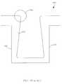
- the resulting profileincludes an “overhang” at the top of the via as illustrated in FIG. 1.
- a via 100comprises two sidewalls 102 and a TiN liner 103 with an “overhang” 104 .
- the overhang 104affects the nucleation film as the depositing tungsten generally grows away from the surface.
- the tungsten nucleation film growthis in a direction perpendicular to the surface of the sidewalls.
- the tungsten nucleation filmwill grow conforming to the existing overhang 104 from the TiN liner 103 and the top area of the via will close prematurely, creating a void.
- step coverageThe uniformity of a deposited film in patterned features like a trench or a via (such as the TiN liner 103 ) is referred to as “step coverage”.
- the step coverageis typically determined by taking a ratio of the maximum thickness and the minimum thickness and converting the value to a percentage.
- a 60% step coverage of the TiN liner 103may indicate a maximum thickness of about 10 nanometers (nm) at the top of a via and a minimum thickness of about 6 nm at the bottom of the via sidewall.
- the goalis to have 100% step coverage for a TiN liner deposition.
- the problem of the step coverage for a TiN lineris increased.
- Substantial thinning of a TiN liner near the bottom of via sidewallis evident and illustrated with the TiN liner 103 of FIG. 1 .
- the poor step coverage in the TiN liner 103results in poor step coverage of the tungsten nucleation film. It is also conceivable that non-uniformity during the via etch process can result in areas without any liner coverage. The absence of any liner coverage reduces the growth rate of the tungsten nucleation film.
- Solutions to resolve the voiding probleminclude varying the tungsten film chemistry, the tungsten nucleation film thickness, and the TiN liner thickness.
- the TiN liner thickness in comparison with the tungsten nucleation film thicknessis almost negligible.
- the liner thicknessis about 10 nm and the tungsten nucleation film thickness is about 100 nm.
- the overhang profile created during the TiN liner depositiontherefore, is more pronounced after forming the tungsten nucleation film.
- the step coveragebecomes worse as the overhang profile from the TiN liner is more pronounced.
- tungsten nucleation film with a thickness that is too thinforms a by-product called hydrogen fluoride (HF) which attacks the TiN liner and creates defects known as “woil holes” that results when the WF 6 gas contacts the silicon.
- HFhydrogen fluoride
- FIG. 1is a cross-section view of a via including a TiN liner with an overhang profile, that is commonly known to those skilled in the art.
- FIG. 2is a block diagram illustrating an exemplary wafer processing system according to an embodiment of the present invention.
- FIG. 3is a flow chart illustrating an exemplary application in a wafer fabrication sequence according to an embodiment of the present invention.
- FIG. 4is a flow chart illustrating an exemplary tungsten via fill process including a 2-step nucleation film growth according to an embodiment of the present invention.
- the present inventionprovides an apparatus and method of depositing a tungsten film including a controlled first nucleation film growth and a second nucleation film growth.
- the first nucleation film growthincludes a first silane-rich nucleation (or “seed”) layer achieved by flowing a significantly higher ratio of silane-containing gas and the second nucleation film growth includes a second tungsten nucleation layer by flowing a higher ratio of tungsten-containing gas.
- Having the first and second nucleation film growthsresult in uniform step coverage of a nucleation film and provides process stability as the sensitivity associated with MFC response time is eliminated.
- the potential for gas phase nucleationis also minimized as the deposition occurs at a lower pressure regime. In addition, contact resistance and chain contact resistance is reduced significantly.
- FIG. 2is a block diagram illustrating an exemplary embodiment of a wafer fabricating system 200 comprising a film depositing system 230 coupled to a control system 234 .
- the film depositing system 230further comprises a reaction chamber 217 coupled to a pump exhaust 218 and a vacuum pump 215 .
- Interior to the reaction chamber 217is a gas mixing block 210 that is connected to a showerhead 212 , and a substrate heating source 214 .
- the substrate heating source 214is a resistive heater.
- the substrate heating source 214may also be a radio frequency (RF) power generator or an infrared lamp source.
- the ends of the substrate heating source 214arc capped with ceramic liners 216 which prevent the gas species from flowing under the substrate heating source 214 and contains the gas species within the reaction chamber 217 .
- RFradio frequency
- a substrate 211rests upon the substrate heating source 214 during the film deposition process.
- An argon gas source 225 coupled to the substrate heating source 214controls the pressure interfacing the backside of the substrate 211 (backside pressure).
- the backside pressureis less than the pressure in the reaction chamber 217 allowing the substrate 211 to be held in place.
- a wafer susceptoris placed closely above the substrate heating source 214 .
- the substrate 211rests on top of the water susceptor.
- the substrate 211may be a semiconductor substrate of silicon or a wafer including multiple devices.
- a robotic lift 222is used to control the up and down motion of the substrate heating source 214 in order to place the substrate 211 in or out of the reaction chamber 217 .
- the reaction chamber 217should be capable of withstanding corrosive gases such as HF, WF 6 , or titanium tetrachloride (TiCl 4 ).
- the film depositing system 230comprises a tungsten-containing gas source 224 and a silane-containing gas source 226 , each interfacing the gas mixing block 210 that, in turn, introduces the gas mixture into the reaction chamber 217 .
- the tungsten-containing gas source 224is WF 6 and the silane-containing gas source 226 is SiH 4 .
- a diluent gas source 228 and two gas sources 227 and 229which may include hydrogen (H 2 ) and nitrogen (N 2 ), respectively.
- the diluent gas source 228 and the gas source (H 2 ) 227are further connected to the substrate heating source 214 to provide an edge purge at the surface interfacing the substrate 211 .
- the general mechanism of depositing a tungsten filmincludes creating a nucleation film (nucleation film growth) and depositing a bulk layer (bulk tungsten film deposition) by introducing a given composition of a gas mixture into a reaction chamber.
- a gas mixture from the tungsten-containing gas source 224 and the silane-containing gas source 226is fed through the gas mixing block 210 and into the reaction chamber 217 .
- the gas mixture from the gas mixing block 210is distributed through the showerhead 212 .
- the gas mixturethen moves to the substrate 211 where the reactants are absorbed on the surface.
- the absorbed atomsundergo migration and film forming chemical reactions.
- the resulting gaseous by-products of the reactionare desorbed and removed from the reaction chamber 217 through the pump exhaust 218 .
- the energy to drive the reactionscan be supplied by several methods (such as thermal, photons or electrons), in which thermal energy is the most commonly used.
- the substrate 211is heated using the substrate heating source 214 .
- the substrate heating source 214enhances the surface reaction of a depositing surface in the substrate 211 during the nucleation film growth and the bulk tungsten deposition.
- the wafer substrate 211can be heated using radio frequency (RF) induction heating, photons, energy from a plasma or energy from infrared lamps.
- RFradio frequency
- the reactant gasesare carried by diluent gases supplied from a gas source such as the diluent gas source 228 in the film depositing system 230 .
- the diluent gasesenhance the uniformity of the tungsten film and may be inert gases.
- the diluent gas source 228is argon (Ar).
- Other already disclosed gases that could be used as the diluent gasinclude H 2 or N 2 .
- the gas source (H 2 ) 227is integral during the bulk tungsten deposition and the gas source (N 2 ) 229 is important in controlling the grain size of the depositing film throughout the overall film deposition process, including the nucleation film growth.
- the diluent gas source 228 and the gas source (H 2 ) 227are introduced from the substrate heating source 214 to provide an edge purge at the surface interfacing the substrate 211 .
- the edge purgeallows controllability in uniformity of the overall tungsten film. For example, by increasing the argon flow, the tungsten film thickness is thinner around the edge of the substrate 211 than the center. On the other hand, the tungsten film thickness is greater around the edge of the substrate 211 when increasing the hydrogen flow.
- the control system 234may consist of one or more input devices that allow an operator to enter a set of conditions known as a process “recipe” needed to achieve the desired deposition process.
- the control system 234may include, for example, a monitor, a touch screen, and related control circuitry that enable an operator to manually enter a recipe for execution by the control circuitry.
- the control system 234can include a computer 236 and related input/output devices coupled thereto, such as a monitor 238 , a keyboard 240 , a mouse 242 , and one or more storage devices 244 .
- the storage devices 244may include any one or any combination of floppy disc drives, hard disc drives, CD-ROM drives, tape drives, etc.
- the computer 236typically includes a processor and memory, such as any combination of read-only memory (ROM), random access memory (RAM), etc.
- the computer 236employs an application program that receives and executes each recipe to control the reaction chamber 217 and its included components.
- the recipemay comprise a set of instructions in the form of a software program or the like so that one or more such recipes may be created and stored on the storage device 244 .
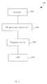
- FIG. 3is a flow chart illustrating an exemplary application in a wafer fabrication sequence according to an embodiment of the present invention.
- the flow chart 300illustrates a wafer fabrication sequence comprising a via etch in block 302 in which vias are formed within the semiconductor substrate or wafer to connect one layer of metal to another layer of metal.
- a TiN glue lineris deposited onto the sidewalls and at the bottom of the vias during the TiN deposition in block 304 .
- the TiN lineracts as an adhesive for a tungsten via fill performed in a different processing tool in the following block 306 .
- a tungsten materialis generally used to fill a via because of its low resistivity. Accordingly, a chemical mechanical planarization (CMP) block 312 is performed to planarize the tungsten via fill.
- CMPchemical mechanical planarization
- FIG. 4is a flow chart that further illustrates an exemplary tungsten film deposition process recipe for the tungsten via fill in block 306 including a 2-step nucleation film growth according to the present invention.
- the process recipeincludes executing a first nucleation film growth and a second nucleation film growth to foil a nucleation film preceding the bulk tungsten film deposition.
- the exemplary tungsten film deposition process recipe including the first and second nucleation growths subsequently followed by the bulk tungsten film depositionmay be performed using a single processing tool.
- the tungsten via fill in block 306can be achieved performing the tungsten film deposition process recipe in an embodiment similar to the wafer fabricating system 200 described previously.
- the substrate 211is loaded into the reaction chamber 217 by first placing the substrate 211 on the substrate heating source 214 in block 402 .
- the control system 234then instructs the robotic lift 222 to raise the substrate heating source 214 so that the distance from the substrate heating source 214 and the showerhead 212 is at a value within the range of about 375 milli inch (mils) and 425 mils.
- the substrate heating source 214is then prompted to heat the substrate 211 at a temperature within the range of approximately 400 degrees Celsius and 450 degrees Celsius in block 404 . Both the spacing and the temperature of the substrate heating Source 214 are maintained throughout the tungsten film deposition process.
- the control system 234instructs the diluent gas source 228 , the gas source (N 2 ) 229 , and the silane-containing gas source 226 to flow a sufficient amount of a silicide gas mixture comprising argon, nitrogen, and silane for a “silane soak.”
- the silane soakenhances the tungsten film uniformity by forming a very thin, protective layer of amorphous silicon on the surface upon which the tungsten film is to be deposited.
- the protective layerpromotes the adhesion of the tungsten film.
- the silane soakis performed by applying pressure and sequentially ramping the pressure from approximately 4.5 torr to approximately 10 torr to approximately 30 torr. In one embodiment, the pressure is ramped during a period of time on the order of approximately 15 to 20 seconds. In particular, the pressure is ramped over three equivalent time segments such as 5 seconds each. By ramping the pressure, the wafer chucking capability is improved.
- a first nucleation film growthis performed in block 406 by flowing silane gas from a silane containing gas source 226 at a first flow rate, and tungsten gas from a tungsten-containing gas source 224 at the second flow rate, where the first flow rate is significantly greater than the second flow rate, and for a period of time sufficient to provide a first silane-rich nucleation layer.
- the period of time to provide a first silane-rich nucleation layeris approximately 5 seconds.
- the control system 234instructs the tungsten-containing gas source 224 and the silane-containing gas source 226 to flow a sufficient amount of gas mixture that results in a first silane-rich nucleation site layer that acts as a “seed” layer for the subsequent second nucleation film growth and the bulk tungsten film deposition. It is conceivable that the “seed” layer nucleates uniformly on all the surfaces within the via and, therefore, covers up any region or location devoid of the TiN glue liner, such as the bottom corners of a via.
- the gas flow rate ratio of the first flow rate and the second flow rateis within the range of approximately 2:1 to 7:1. More specifically, the control system 234 instructs the silane-containing gas source 226 and the tungsten-containing gas source 224 to flow SiH 4 and WF 6 at a ratio within the range of approximately 2:1 to 7:1.
- the tungsten-containing gas source 224is prompted to flow WF 6 gas at a rate within the range of approximately 5 to 10 standard cubic centimeter per minute (sccm).
- the silane-containing gas source 226allows the SiH 4 gas to flow at a rate within the range of approximately 27 to 33 sccm.
- the control system 234further instructs the diluent as source 228 to flow a sufficient amount of diluent gas in order to enhance uniformity across the substrate 211 .
- an argon gas supplied by the diluent as source 228flows at a rate of approximately 1000 sccm through the mixing block 210 .
- the gas sources 227 and 229are also prompted to flow H, and N, at approximately 1000 sccm and approximately 300 sccm, respectively.
- the gas mixture in the gas mixing block 210is dispersed into the reaction chamber 217 by the showerhead 212 .
- control system 234also instructs the diluent gas source 228 to flow argon from the substrate heating source 214 to provide an edge purge at the surface interfacing the substrate 211 .
- control system 234instructs the diluent gas source 228 to flow argon at a rate within the range of approximately 250 to 550 sccm.
- a second nucleation film growthis performed in block 408 by flowing silanie as from a silane-containing as source 226 a t a first flow rate and tungsten n gas from a tungsten-containing as source 224 at a second flow rate, where the second flow rate is greater than the first flow rate, and for a period of time sufficient to deposit a second tungsten nucleation layer with the desired thickness.
- a as flow rate ratio of the first flow rate and the second flow rateis a value within the range of approximately 1:1.9 to 1:2.1.
- the control system 234instructs the silane-containing gas source 226 and the tungsten-containing as source 224 to flow SiH 4 and WF 6 at a ratio of approximately 1:2.
- control system 234instructs the silane-containing gas source 226 to flow at a rate within the range of approximately 4 to 6 sccm of SiH, and the tungsten-containing, gas source 224 to flow at a rate within the range of approximately 8 to 12 sccm of WF 6 .
- the control system 234further instructs the diluent gas source 228 to flow argon gas at a rate of approximately 1,000 sccm. In one embodiment, the control system 234 also instructs the diluent gas source 228 to flow argon from the substrate heating source 214 to provide an edge purge at the surface interfacing the substrate 211 . In particular, the control system 234 instructs the diluent gas source 228 to flow argon at a rate within the range of approximately 250 to 550 sccm. The gas sources 227 and 229 are prompted to flow H 2 and N 2 at approximately 1,000 sccm and approximately 300 sccm, respectively.
- the increased tungsten gas flow rate ratio of the second tungsten nucleation layeroptimizes the overall nucleation film thickness.
- the period of time in which the control system 234 instructs the gas sources 224 , 226 , 227 , 228 , and 229 to flowvaries depending on the target thickness of the nucleation film.
- the second tungsten nucleation layer deposition of block 408occurs for a period of time within approximately 19 to 29 seconds in order to obtain approximately 10 to 60 nm of the nucleation film.
- the particular range of thicknesswas determined to minimize the WF 6 reaction with the TiN liner material and to ensure complete coverage of the liner surface.
- Forming the overall nucleation film thicknessfurther requires achieving and maintaining a sufficiently low pressure in the reaction chamber 217 while executing the first nucleation film growth in block 406 and a second nucleation film growth in block 408 .
- the control system 234instructs the vacuum pump 215 to pressurize the reaction chamber 217 at a pressure within the range of approximately 3 to 6 torr. In a more specific embodiment, the control system 234 instructs the vacuum pump 215 to pressurize the reaction chamber 217 at approximately 4.5 torr.
- a bulk layer of tungsten filmis further deposited (bulk tungsten film deposition) by flowing a tungsten-rich gas mixture while maintaining a sufficient pressure.
- the control system 234instructs the vacuum pump 215 to increase the pressure in the reaction chamber 217 to about 90 torr.
- the tungsten-containing as source 224is prompted to flow WF 6 at a rate ranging within approximately 90 to 100 sccm.
- the gas source (H 2 ) 227is instructed to flow within the range of approximately 1500 to 2100 sccm of H 2 .
- the diluent as source 228 and the gas Source (N 2 ) 229flow a Sufficient amount of gas mixture as described in the previous block 408 .
- the reaction chamber 217is purged to atmospheric pressure in block 412 and the robotic lift 222 is prompted to lower the substrate heating source 214 alone with the substrate 211 .
- the substrate 211is removed from the reaction chamber 217 in block 414 .
- the resulting benefits of the present inventionincludes a significant reduction in sensitivity towards gas phase nucleation and an improvement in the nucleation step coverage resulting from the lower partial pressures of the process gases and slower deposition rates.
- the first nucleation film growthallows the seed layer to nucleate uniformly on all the Surfaces within the via and, therefore, covers up any region or location devoid of the TiN glue liner.
- the second nucleation film growthprovides a more accurate controllability to optimize the overall nucleation film thickness.
- the step coverage for the 2-step nucleation tungsten via fill processis approximately 80%. Consequently, there is an improvement in the via fill characteristics.
- the method of depositing a tungsten film in the application of achieving superior via fill according to the present inventioncan be utilized in the fabrication of various devices such as a Dynamic Random Access Memory (DRAM) or Logic applications.
- DRAMDynamic Random Access Memory
- the present inventionhas been described in one or more embodiments that are to be illustrative and not restrictive. It should also be apparent that such other alternatives, modifications and variations may be effected without departing from the spirit and scope of the present invention.
- the present inventioncan be applied for developing interconnects or metal lines in which a low resistance of the material is desired. The scope of the invention should, therefore, be determined not with reference to the above descriptions, but instead to the appended claims.
Landscapes
- Engineering & Computer Science (AREA)
- Microelectronics & Electronic Packaging (AREA)
- Condensed Matter Physics & Semiconductors (AREA)
- General Physics & Mathematics (AREA)
- Manufacturing & Machinery (AREA)
- Computer Hardware Design (AREA)
- Physics & Mathematics (AREA)
- Power Engineering (AREA)
- Chemical & Material Sciences (AREA)
- Crystallography & Structural Chemistry (AREA)
- Chemical Kinetics & Catalysis (AREA)
- General Chemical & Material Sciences (AREA)
- Electrodes Of Semiconductors (AREA)
- Chemical Vapour Deposition (AREA)
Abstract
Description
Claims (10)
Priority Applications (1)
| Application Number | Priority Date | Filing Date | Title |
|---|---|---|---|
| US09/639,183US6309966B1 (en) | 1999-09-03 | 2000-08-15 | Apparatus and method of a low pressure, two-step nucleation tungsten deposition |
Applications Claiming Priority (2)
| Application Number | Priority Date | Filing Date | Title |
|---|---|---|---|
| US15240799P | 1999-09-03 | 1999-09-03 | |
| US09/639,183US6309966B1 (en) | 1999-09-03 | 2000-08-15 | Apparatus and method of a low pressure, two-step nucleation tungsten deposition |
Publications (1)
| Publication Number | Publication Date |
|---|---|
| US6309966B1true US6309966B1 (en) | 2001-10-30 |
Family
ID=26849529
Family Applications (1)
| Application Number | Title | Priority Date | Filing Date |
|---|---|---|---|
| US09/639,183Expired - LifetimeUS6309966B1 (en) | 1999-09-03 | 2000-08-15 | Apparatus and method of a low pressure, two-step nucleation tungsten deposition |
Country Status (1)
| Country | Link |
|---|---|
| US (1) | US6309966B1 (en) |
Cited By (68)
| Publication number | Priority date | Publication date | Assignee | Title |
|---|---|---|---|---|
| US6489239B1 (en)* | 1999-12-06 | 2002-12-03 | Samsung Electronics Co., Ltd. | Method of tungsten chemical vapor deposition and tungsten plug formation |
| US20030003729A1 (en)* | 2000-11-17 | 2003-01-02 | Hideaki Yamasaki | Method of forming metal wiring and semiconductor manufacturing apparatus for forming metal wiring |
| US20030119303A1 (en)* | 2000-01-24 | 2003-06-26 | Tomoyuki Morita | Method of forming a patterned tungsten damascene interconnect |
| US6635965B1 (en)* | 2001-05-22 | 2003-10-21 | Novellus Systems, Inc. | Method for producing ultra-thin tungsten layers with improved step coverage |
| US6699788B2 (en)* | 2001-11-13 | 2004-03-02 | Chartered Semiconductors Manufacturing Limited | Method for integrated nucleation and bulk film deposition |
| US20040142557A1 (en)* | 2003-01-21 | 2004-07-22 | Novellus Systems, Inc. | Deposition of tungsten nitride |
| US20040202786A1 (en)* | 2001-05-22 | 2004-10-14 | Novellus Systems, Inc. | Method of forming low-resistivity tungsten interconnects |
| US20040224486A1 (en)* | 2001-07-10 | 2004-11-11 | Semiconductor Energy Laboratory Co., Ltd. | Semiconductor film, semiconductor device, and manufacturing method thereof |
| US20050020037A1 (en)* | 2001-06-01 | 2005-01-27 | Semiconductor Energy Laboratory Co., Ltd. | Semiconductor film, semiconductor device and method of their production |
| US20050032364A1 (en)* | 2001-08-14 | 2005-02-10 | Kazuya Okubo | Method of forming tungsten film |
| US20050031786A1 (en)* | 2001-05-22 | 2005-02-10 | Novellus Systems, Inc. | Method for reducing tungsten film roughness and improving step coverage |
| US20050079656A1 (en)* | 2001-09-27 | 2005-04-14 | Semiconductor Energy Laboratory Co., Ltd. | Method of manufacturing a semiconductor device |
| US20060009034A1 (en)* | 2000-06-28 | 2006-01-12 | Lai Ken K | Methods for depositing tungsten layers employing atomic layer deposition techniques |
| US7157798B1 (en) | 2003-05-09 | 2007-01-02 | Novellus Systems, Inc. | Selective refractory metal and nitride capping |
| US20070087560A1 (en)* | 2005-10-14 | 2007-04-19 | Samsung Electronics Co., Ltd. | Method of manufacturing semiconductor device |
| US20080045010A1 (en)* | 2003-08-26 | 2008-02-21 | Novellus Systems, Inc. | Reducing silicon attack and improving resistivity of tungsten nitride film |
| US20080124926A1 (en)* | 2001-05-22 | 2008-05-29 | Novellus Systems, Inc. | Methods for growing low-resistivity tungsten film |
| US20080202425A1 (en)* | 2007-01-29 | 2008-08-28 | Applied Materials, Inc. | Temperature controlled lid assembly for tungsten nitride deposition |
| US20090004848A1 (en)* | 2007-06-28 | 2009-01-01 | Choon Hwan Kim | Method for fabricating interconnection in semiconductor device |
| US20090032949A1 (en)* | 2007-08-02 | 2009-02-05 | Micron Technology, Inc. | Method of depositing Tungsten using plasma-treated tungsten nitride |
| US20090114832A1 (en)* | 2007-08-30 | 2009-05-07 | Kelvin Lynn | Semiconductive materials and associated uses thereof |
| US20090149022A1 (en)* | 2007-12-05 | 2009-06-11 | Novellus Systems, Inc. | Method for improving uniformity and adhesion of low resistivity tungsten film |
| US20090163025A1 (en)* | 2007-12-21 | 2009-06-25 | Novellus Systems, Inc. | Methods for forming all tungsten contacts and lines |
| US7595263B2 (en) | 2003-06-18 | 2009-09-29 | Applied Materials, Inc. | Atomic layer deposition of barrier materials |
| US7605083B2 (en) | 2001-07-16 | 2009-10-20 | Applied Materials, Inc. | Formation of composite tungsten films |
| US7611990B2 (en) | 2001-07-25 | 2009-11-03 | Applied Materials, Inc. | Deposition methods for barrier and tungsten materials |
| US20090275197A1 (en)* | 2008-04-30 | 2009-11-05 | Nec Electronics Corporation | Method for manufacturing semiconductor device |
| US7655567B1 (en) | 2007-07-24 | 2010-02-02 | Novellus Systems, Inc. | Methods for improving uniformity and resistivity of thin tungsten films |
| US20100055904A1 (en)* | 2008-08-29 | 2010-03-04 | Novellus Systems Inc. | Method for reducing tungsten roughness and improving reflectivity |
| US7695563B2 (en) | 2001-07-13 | 2010-04-13 | Applied Materials, Inc. | Pulsed deposition process for tungsten nucleation |
| US7732327B2 (en) | 2000-06-28 | 2010-06-08 | Applied Materials, Inc. | Vapor deposition of tungsten materials |
| US20100159694A1 (en)* | 2008-06-12 | 2010-06-24 | Novellus Systems Inc. | Method for depositing thin tungsten film with low resistivity and robust micro-adhesion characteristics |
| US7745329B2 (en) | 2002-02-26 | 2010-06-29 | Applied Materials, Inc. | Tungsten nitride atomic layer deposition processes |
| US7749815B2 (en) | 2001-07-16 | 2010-07-06 | Applied Materials, Inc. | Methods for depositing tungsten after surface treatment |
| US20100267230A1 (en)* | 2009-04-16 | 2010-10-21 | Anand Chandrashekar | Method for forming tungsten contacts and interconnects with small critical dimensions |
| US7867914B2 (en) | 2002-04-16 | 2011-01-11 | Applied Materials, Inc. | System and method for forming an integrated barrier layer |
| US20110059608A1 (en)* | 2009-09-09 | 2011-03-10 | Novellus Systems, Inc. | Method for improving adhesion of low resistivity tungsten/tungsten nitride layers |
| US7955972B2 (en) | 2001-05-22 | 2011-06-07 | Novellus Systems, Inc. | Methods for growing low-resistivity tungsten for high aspect ratio and small features |
| US7964505B2 (en) | 2005-01-19 | 2011-06-21 | Applied Materials, Inc. | Atomic layer deposition of tungsten materials |
| US20110221044A1 (en)* | 2010-03-12 | 2011-09-15 | Michal Danek | Tungsten barrier and seed for copper filled tsv |
| US8062977B1 (en) | 2008-01-31 | 2011-11-22 | Novellus Systems, Inc. | Ternary tungsten-containing resistive thin films |
| US8853080B2 (en) | 2012-09-09 | 2014-10-07 | Novellus Systems, Inc. | Method for depositing tungsten film with low roughness and low resistivity |
| US8859417B2 (en) | 2013-01-03 | 2014-10-14 | Globalfoundries Inc. | Gate electrode(s) and contact structure(s), and methods of fabrication thereof |
| US8975184B2 (en) | 2012-07-27 | 2015-03-10 | Novellus Systems, Inc. | Methods of improving tungsten contact resistance in small critical dimension features |
| US9034760B2 (en) | 2012-06-29 | 2015-05-19 | Novellus Systems, Inc. | Methods of forming tensile tungsten films and compressive tungsten films |
| US9076843B2 (en) | 2001-05-22 | 2015-07-07 | Novellus Systems, Inc. | Method for producing ultra-thin tungsten layers with improved step coverage |
| US9153486B2 (en) | 2013-04-12 | 2015-10-06 | Lam Research Corporation | CVD based metal/semiconductor OHMIC contact for high volume manufacturing applications |
| US9159571B2 (en) | 2009-04-16 | 2015-10-13 | Lam Research Corporation | Tungsten deposition process using germanium-containing reducing agent |
| US9240347B2 (en) | 2012-03-27 | 2016-01-19 | Novellus Systems, Inc. | Tungsten feature fill |
| US9589808B2 (en) | 2013-12-19 | 2017-03-07 | Lam Research Corporation | Method for depositing extremely low resistivity tungsten |
| US9613818B2 (en) | 2015-05-27 | 2017-04-04 | Lam Research Corporation | Deposition of low fluorine tungsten by sequential CVD process |
| US9754824B2 (en) | 2015-05-27 | 2017-09-05 | Lam Research Corporation | Tungsten films having low fluorine content |
| US20170309490A1 (en)* | 2014-09-24 | 2017-10-26 | Hitachi Kokusai Electric Inc. | Method of manufacturing semiconductor device |
| US9953984B2 (en) | 2015-02-11 | 2018-04-24 | Lam Research Corporation | Tungsten for wordline applications |
| US9978605B2 (en) | 2015-05-27 | 2018-05-22 | Lam Research Corporation | Method of forming low resistivity fluorine free tungsten film without nucleation |
| US9997405B2 (en) | 2014-09-30 | 2018-06-12 | Lam Research Corporation | Feature fill with nucleation inhibition |
| DE102017216937A1 (en) | 2017-09-25 | 2019-03-28 | Robert Bosch Gmbh | Method for producing at least one via in a wafer |
| US10256142B2 (en) | 2009-08-04 | 2019-04-09 | Novellus Systems, Inc. | Tungsten feature fill with nucleation inhibition |
| US10867808B1 (en) | 2019-07-09 | 2020-12-15 | United Microelectronics Corp. | Manufacturing method of connection structure |
| US11348795B2 (en) | 2017-08-14 | 2022-05-31 | Lam Research Corporation | Metal fill process for three-dimensional vertical NAND wordline |
| US11549175B2 (en) | 2018-05-03 | 2023-01-10 | Lam Research Corporation | Method of depositing tungsten and other metals in 3D NAND structures |
| CN115928040A (en)* | 2022-11-30 | 2023-04-07 | 上海华虹宏力半导体制造有限公司 | Tungsten Chemical Vapor Deposition Method |
| US11972952B2 (en) | 2018-12-14 | 2024-04-30 | Lam Research Corporation | Atomic layer deposition on 3D NAND structures |
| US12002679B2 (en) | 2019-04-11 | 2024-06-04 | Lam Research Corporation | High step coverage tungsten deposition |
| US12077858B2 (en) | 2019-08-12 | 2024-09-03 | Lam Research Corporation | Tungsten deposition |
| US12237221B2 (en) | 2019-05-22 | 2025-02-25 | Lam Research Corporation | Nucleation-free tungsten deposition |
| US12426515B2 (en) | 2021-10-26 | 2025-09-23 | United Microelectronics Corp. | Semiconductor device and method for fabricating the same |
| US12444651B2 (en) | 2022-06-28 | 2025-10-14 | Novellus Systems, Inc. | Tungsten feature fill with nucleation inhibition |
Citations (5)
| Publication number | Priority date | Publication date | Assignee | Title |
|---|---|---|---|---|
| US5489552A (en)* | 1994-12-30 | 1996-02-06 | At&T Corp. | Multiple layer tungsten deposition process |
| US5661080A (en)* | 1992-12-10 | 1997-08-26 | Hyundai Electronics Industries Co., Ltd. | Method for fabricating tungsten plug |
| US5795824A (en)* | 1997-08-28 | 1998-08-18 | Novellus Systems, Inc. | Method for nucleation of CVD tungsten films |
| WO1999028527A1 (en)* | 1997-12-03 | 1999-06-10 | Applied Materials, Inc. | Method and apparatus for forming a metal layer |
| US5956609A (en)* | 1997-08-11 | 1999-09-21 | Taiwan Semiconductor Manufacturing Company, Ltd. | Method for reducing stress and improving step-coverage of tungsten interconnects and plugs |
- 2000
- 2000-08-15USUS09/639,183patent/US6309966B1/ennot_activeExpired - Lifetime
Patent Citations (5)
| Publication number | Priority date | Publication date | Assignee | Title |
|---|---|---|---|---|
| US5661080A (en)* | 1992-12-10 | 1997-08-26 | Hyundai Electronics Industries Co., Ltd. | Method for fabricating tungsten plug |
| US5489552A (en)* | 1994-12-30 | 1996-02-06 | At&T Corp. | Multiple layer tungsten deposition process |
| US5956609A (en)* | 1997-08-11 | 1999-09-21 | Taiwan Semiconductor Manufacturing Company, Ltd. | Method for reducing stress and improving step-coverage of tungsten interconnects and plugs |
| US5795824A (en)* | 1997-08-28 | 1998-08-18 | Novellus Systems, Inc. | Method for nucleation of CVD tungsten films |
| WO1999028527A1 (en)* | 1997-12-03 | 1999-06-10 | Applied Materials, Inc. | Method and apparatus for forming a metal layer |
Non-Patent Citations (7)
| Title |
|---|
| Broadbent and Stacy, "Selective tungsten processing by low pressure CVD," Solid State Technology, pp. 51-59, Dec. 1985. |
| Broadbent, "Nucleation and growth of chemically vapor deposited tungsten on various substrate materials: A review," J. Vac. Sci. Technol., B 5(6):1161-1666, Nov./Dec. 1987. |
| Clark, "Response surface modeling of high pressure chemical vapor deposited blanket tungsten," J. Vac. Sci. Technol., B 9(3):1478-1486, May/Jun. 1991. |
| Kim et al., "Studies on the nucleation and growth of chemical-vapor-deposited W on TiN substrates," Materials Science and Engineering, B17:1377-142, 1993. |
| Riley and Clark, "Integrated chemical vapor deposition and plasma etchback of tungsten in a multichamber, single-wafer system," J. Electrochem. Soc., 138(10):3008-3013, Oct. 1991. |
| Schmitz, "Chemical vapor deposition of tungsten and tungsten silicides for VLSI/ULSI applications," Noyes Publications, Park Ridge, New Jersey, 1992. |
| Wells, "Tungsten and other refractory metals for VLSI applications III," Proceedings of the 1987 Workshop, IBM Thomas J. Watson Research Center, Yorktown Heights, New York, U.S.A., pp. 209-216, Oct. 7-9, 1987. |
Cited By (114)
| Publication number | Priority date | Publication date | Assignee | Title |
|---|---|---|---|---|
| US6489239B1 (en)* | 1999-12-06 | 2002-12-03 | Samsung Electronics Co., Ltd. | Method of tungsten chemical vapor deposition and tungsten plug formation |
| US20030119303A1 (en)* | 2000-01-24 | 2003-06-26 | Tomoyuki Morita | Method of forming a patterned tungsten damascene interconnect |
| US6780764B2 (en)* | 2000-01-24 | 2004-08-24 | Oki Electric Industry Co., Ltd. | Method of forming a patterned tungsten damascene interconnect |
| US7732327B2 (en) | 2000-06-28 | 2010-06-08 | Applied Materials, Inc. | Vapor deposition of tungsten materials |
| US7405158B2 (en)* | 2000-06-28 | 2008-07-29 | Applied Materials, Inc. | Methods for depositing tungsten layers employing atomic layer deposition techniques |
| US20060009034A1 (en)* | 2000-06-28 | 2006-01-12 | Lai Ken K | Methods for depositing tungsten layers employing atomic layer deposition techniques |
| US7745333B2 (en) | 2000-06-28 | 2010-06-29 | Applied Materials, Inc. | Methods for depositing tungsten layers employing atomic layer deposition techniques |
| US20030003729A1 (en)* | 2000-11-17 | 2003-01-02 | Hideaki Yamasaki | Method of forming metal wiring and semiconductor manufacturing apparatus for forming metal wiring |
| US6913996B2 (en)* | 2000-11-17 | 2005-07-05 | Tokyo Electron Limited | Method of forming metal wiring and semiconductor manufacturing apparatus for forming metal wiring |
| US8048805B2 (en) | 2001-05-22 | 2011-11-01 | Novellus Systems, Inc. | Methods for growing low-resistivity tungsten film |
| US20110223763A1 (en)* | 2001-05-22 | 2011-09-15 | Lana Hiului Chan | Methods for growing low-resistivity tungsten for high aspect ratio and small features |
| US20050031786A1 (en)* | 2001-05-22 | 2005-02-10 | Novellus Systems, Inc. | Method for reducing tungsten film roughness and improving step coverage |
| US7955972B2 (en) | 2001-05-22 | 2011-06-07 | Novellus Systems, Inc. | Methods for growing low-resistivity tungsten for high aspect ratio and small features |
| US20100035427A1 (en)* | 2001-05-22 | 2010-02-11 | Novellus Systems, Inc. | Methods for growing low-resistivity tungsten film |
| US20040202786A1 (en)* | 2001-05-22 | 2004-10-14 | Novellus Systems, Inc. | Method of forming low-resistivity tungsten interconnects |
| US7589017B2 (en) | 2001-05-22 | 2009-09-15 | Novellus Systems, Inc. | Methods for growing low-resistivity tungsten film |
| US9076843B2 (en) | 2001-05-22 | 2015-07-07 | Novellus Systems, Inc. | Method for producing ultra-thin tungsten layers with improved step coverage |
| US9583385B2 (en) | 2001-05-22 | 2017-02-28 | Novellus Systems, Inc. | Method for producing ultra-thin tungsten layers with improved step coverage |
| US6635965B1 (en)* | 2001-05-22 | 2003-10-21 | Novellus Systems, Inc. | Method for producing ultra-thin tungsten layers with improved step coverage |
| US8409985B2 (en) | 2001-05-22 | 2013-04-02 | Novellus Systems, Inc. | Methods for growing low-resistivity tungsten for high aspect ratio and small features |
| US20080124926A1 (en)* | 2001-05-22 | 2008-05-29 | Novellus Systems, Inc. | Methods for growing low-resistivity tungsten film |
| US7262125B2 (en) | 2001-05-22 | 2007-08-28 | Novellus Systems, Inc. | Method of forming low-resistivity tungsten interconnects |
| US7141494B2 (en) | 2001-05-22 | 2006-11-28 | Novellus Systems, Inc. | Method for reducing tungsten film roughness and improving step coverage |
| US20050020037A1 (en)* | 2001-06-01 | 2005-01-27 | Semiconductor Energy Laboratory Co., Ltd. | Semiconductor film, semiconductor device and method of their production |
| US7384828B2 (en) | 2001-06-01 | 2008-06-10 | Semiconductor Energy Laboratory Co., Ltd. | Semiconductor film, semiconductor device and method of their production |
| US7199027B2 (en)* | 2001-07-10 | 2007-04-03 | Semiconductor Energy Laboratory Co., Ltd. | Method of manufacturing a semiconductor film by plasma CVD using a noble gas and nitrogen |
| US20040224486A1 (en)* | 2001-07-10 | 2004-11-11 | Semiconductor Energy Laboratory Co., Ltd. | Semiconductor film, semiconductor device, and manufacturing method thereof |
| US7695563B2 (en) | 2001-07-13 | 2010-04-13 | Applied Materials, Inc. | Pulsed deposition process for tungsten nucleation |
| US7749815B2 (en) | 2001-07-16 | 2010-07-06 | Applied Materials, Inc. | Methods for depositing tungsten after surface treatment |
| US7605083B2 (en) | 2001-07-16 | 2009-10-20 | Applied Materials, Inc. | Formation of composite tungsten films |
| US7611990B2 (en) | 2001-07-25 | 2009-11-03 | Applied Materials, Inc. | Deposition methods for barrier and tungsten materials |
| US20050032364A1 (en)* | 2001-08-14 | 2005-02-10 | Kazuya Okubo | Method of forming tungsten film |
| US7592256B2 (en)* | 2001-08-14 | 2009-09-22 | Tokyo Electron Limited | Method of forming tungsten film |
| US7442592B2 (en) | 2001-09-27 | 2008-10-28 | Semiconductor Energy Laboratory Co., Ltd. | Manufacturing a semiconductor device |
| US7109074B2 (en) | 2001-09-27 | 2006-09-19 | Semiconductor Engery Laboratory Co., Ltd. | Method of manufacturing a semiconductor device |
| US20050079656A1 (en)* | 2001-09-27 | 2005-04-14 | Semiconductor Energy Laboratory Co., Ltd. | Method of manufacturing a semiconductor device |
| US20070004109A1 (en)* | 2001-09-27 | 2007-01-04 | Semiconductor Energy Laboratory Co., Ltd. | Manufacturing a semiconductor device |
| SG109987A1 (en)* | 2001-11-13 | 2005-04-28 | Chartered Semiconductor Mfg | Method for integrated nucleation and bulk film deposition |
| US6699788B2 (en)* | 2001-11-13 | 2004-03-02 | Chartered Semiconductors Manufacturing Limited | Method for integrated nucleation and bulk film deposition |
| US7745329B2 (en) | 2002-02-26 | 2010-06-29 | Applied Materials, Inc. | Tungsten nitride atomic layer deposition processes |
| US7867914B2 (en) | 2002-04-16 | 2011-01-11 | Applied Materials, Inc. | System and method for forming an integrated barrier layer |
| US7005372B2 (en) | 2003-01-21 | 2006-02-28 | Novellus Systems, Inc. | Deposition of tungsten nitride |
| US7691749B2 (en) | 2003-01-21 | 2010-04-06 | Novellus Systems, Inc. | Deposition of tungsten nitride |
| US20060094238A1 (en)* | 2003-01-21 | 2006-05-04 | Novellus Systems, Inc. | Deposition of tungsten nitride |
| US20040142557A1 (en)* | 2003-01-21 | 2004-07-22 | Novellus Systems, Inc. | Deposition of tungsten nitride |
| US7157798B1 (en) | 2003-05-09 | 2007-01-02 | Novellus Systems, Inc. | Selective refractory metal and nitride capping |
| US7595263B2 (en) | 2003-06-18 | 2009-09-29 | Applied Materials, Inc. | Atomic layer deposition of barrier materials |
| US20080045010A1 (en)* | 2003-08-26 | 2008-02-21 | Novellus Systems, Inc. | Reducing silicon attack and improving resistivity of tungsten nitride film |
| US7754604B2 (en) | 2003-08-26 | 2010-07-13 | Novellus Systems, Inc. | Reducing silicon attack and improving resistivity of tungsten nitride film |
| US7964505B2 (en) | 2005-01-19 | 2011-06-21 | Applied Materials, Inc. | Atomic layer deposition of tungsten materials |
| US20070087560A1 (en)* | 2005-10-14 | 2007-04-19 | Samsung Electronics Co., Ltd. | Method of manufacturing semiconductor device |
| US7235485B2 (en)* | 2005-10-14 | 2007-06-26 | Samsung Electronics Co., Ltd. | Method of manufacturing semiconductor device |
| US8821637B2 (en)* | 2007-01-29 | 2014-09-02 | Applied Materials, Inc. | Temperature controlled lid assembly for tungsten nitride deposition |
| US20080202425A1 (en)* | 2007-01-29 | 2008-08-28 | Applied Materials, Inc. | Temperature controlled lid assembly for tungsten nitride deposition |
| US20090004848A1 (en)* | 2007-06-28 | 2009-01-01 | Choon Hwan Kim | Method for fabricating interconnection in semiconductor device |
| US8101521B1 (en)* | 2007-07-24 | 2012-01-24 | Novellus Systems, Inc. | Methods for improving uniformity and resistivity of thin tungsten films |
| US7655567B1 (en) | 2007-07-24 | 2010-02-02 | Novellus Systems, Inc. | Methods for improving uniformity and resistivity of thin tungsten films |
| US20090032949A1 (en)* | 2007-08-02 | 2009-02-05 | Micron Technology, Inc. | Method of depositing Tungsten using plasma-treated tungsten nitride |
| US20090114832A1 (en)* | 2007-08-30 | 2009-05-07 | Kelvin Lynn | Semiconductive materials and associated uses thereof |
| US20100273327A1 (en)* | 2007-12-05 | 2010-10-28 | Novellus Systems, Inc. | Method for improving uniformity and adhesion of low resistivity tungsten film |
| US7772114B2 (en) | 2007-12-05 | 2010-08-10 | Novellus Systems, Inc. | Method for improving uniformity and adhesion of low resistivity tungsten film |
| US8329576B2 (en) | 2007-12-05 | 2012-12-11 | Novellus Systems, Inc. | Method for improving uniformity and adhesion of low resistivity tungsten film |
| US20090149022A1 (en)* | 2007-12-05 | 2009-06-11 | Novellus Systems, Inc. | Method for improving uniformity and adhesion of low resistivity tungsten film |
| US8367546B2 (en) | 2007-12-21 | 2013-02-05 | Novellus Systems, Inc. | Methods for forming all tungsten contacts and lines |
| US8053365B2 (en) | 2007-12-21 | 2011-11-08 | Novellus Systems, Inc. | Methods for forming all tungsten contacts and lines |
| US20090163025A1 (en)* | 2007-12-21 | 2009-06-25 | Novellus Systems, Inc. | Methods for forming all tungsten contacts and lines |
| US8062977B1 (en) | 2008-01-31 | 2011-11-22 | Novellus Systems, Inc. | Ternary tungsten-containing resistive thin films |
| US7842609B2 (en) | 2008-04-30 | 2010-11-30 | Nec Electronics Corporation | Method for manufacturing semiconductor device |
| US20090275197A1 (en)* | 2008-04-30 | 2009-11-05 | Nec Electronics Corporation | Method for manufacturing semiconductor device |
| US8058170B2 (en) | 2008-06-12 | 2011-11-15 | Novellus Systems, Inc. | Method for depositing thin tungsten film with low resistivity and robust micro-adhesion characteristics |
| US8409987B2 (en) | 2008-06-12 | 2013-04-02 | Novellus Systems, Inc. | Method for depositing thin tungsten film with low resistivity and robust micro-adhesion characteristics |
| US20100159694A1 (en)* | 2008-06-12 | 2010-06-24 | Novellus Systems Inc. | Method for depositing thin tungsten film with low resistivity and robust micro-adhesion characteristics |
| US8551885B2 (en) | 2008-08-29 | 2013-10-08 | Novellus Systems, Inc. | Method for reducing tungsten roughness and improving reflectivity |
| US20100055904A1 (en)* | 2008-08-29 | 2010-03-04 | Novellus Systems Inc. | Method for reducing tungsten roughness and improving reflectivity |
| US9673146B2 (en) | 2009-04-16 | 2017-06-06 | Novellus Systems, Inc. | Low temperature tungsten film deposition for small critical dimension contacts and interconnects |
| US9236297B2 (en) | 2009-04-16 | 2016-01-12 | Novellus Systems, Inc. | Low tempature tungsten film deposition for small critical dimension contacts and interconnects |
| US20100267230A1 (en)* | 2009-04-16 | 2010-10-21 | Anand Chandrashekar | Method for forming tungsten contacts and interconnects with small critical dimensions |
| US8623733B2 (en) | 2009-04-16 | 2014-01-07 | Novellus Systems, Inc. | Methods for depositing ultra thin low resistivity tungsten film for small critical dimension contacts and interconnects |
| US9159571B2 (en) | 2009-04-16 | 2015-10-13 | Lam Research Corporation | Tungsten deposition process using germanium-containing reducing agent |
| US10256142B2 (en) | 2009-08-04 | 2019-04-09 | Novellus Systems, Inc. | Tungsten feature fill with nucleation inhibition |
| US9653353B2 (en) | 2009-08-04 | 2017-05-16 | Novellus Systems, Inc. | Tungsten feature fill |
| US10103058B2 (en) | 2009-08-04 | 2018-10-16 | Novellus Systems, Inc. | Tungsten feature fill |
| US20110059608A1 (en)* | 2009-09-09 | 2011-03-10 | Novellus Systems, Inc. | Method for improving adhesion of low resistivity tungsten/tungsten nitride layers |
| US8207062B2 (en) | 2009-09-09 | 2012-06-26 | Novellus Systems, Inc. | Method for improving adhesion of low resistivity tungsten/tungsten nitride layers |
| US8709948B2 (en) | 2010-03-12 | 2014-04-29 | Novellus Systems, Inc. | Tungsten barrier and seed for copper filled TSV |
| US20110221044A1 (en)* | 2010-03-12 | 2011-09-15 | Michal Danek | Tungsten barrier and seed for copper filled tsv |
| US9240347B2 (en) | 2012-03-27 | 2016-01-19 | Novellus Systems, Inc. | Tungsten feature fill |
| US9034760B2 (en) | 2012-06-29 | 2015-05-19 | Novellus Systems, Inc. | Methods of forming tensile tungsten films and compressive tungsten films |
| US8975184B2 (en) | 2012-07-27 | 2015-03-10 | Novellus Systems, Inc. | Methods of improving tungsten contact resistance in small critical dimension features |
| US8853080B2 (en) | 2012-09-09 | 2014-10-07 | Novellus Systems, Inc. | Method for depositing tungsten film with low roughness and low resistivity |
| US8859417B2 (en) | 2013-01-03 | 2014-10-14 | Globalfoundries Inc. | Gate electrode(s) and contact structure(s), and methods of fabrication thereof |
| US9153486B2 (en) | 2013-04-12 | 2015-10-06 | Lam Research Corporation | CVD based metal/semiconductor OHMIC contact for high volume manufacturing applications |
| US9589808B2 (en) | 2013-12-19 | 2017-03-07 | Lam Research Corporation | Method for depositing extremely low resistivity tungsten |
| US20170309490A1 (en)* | 2014-09-24 | 2017-10-26 | Hitachi Kokusai Electric Inc. | Method of manufacturing semiconductor device |
| US9997405B2 (en) | 2014-09-30 | 2018-06-12 | Lam Research Corporation | Feature fill with nucleation inhibition |
| US10529722B2 (en) | 2015-02-11 | 2020-01-07 | Lam Research Corporation | Tungsten for wordline applications |
| US9953984B2 (en) | 2015-02-11 | 2018-04-24 | Lam Research Corporation | Tungsten for wordline applications |
| US10546751B2 (en) | 2015-05-27 | 2020-01-28 | Lam Research Corporation | Forming low resistivity fluorine free tungsten film without nucleation |
| US9978605B2 (en) | 2015-05-27 | 2018-05-22 | Lam Research Corporation | Method of forming low resistivity fluorine free tungsten film without nucleation |
| US9754824B2 (en) | 2015-05-27 | 2017-09-05 | Lam Research Corporation | Tungsten films having low fluorine content |
| US9613818B2 (en) | 2015-05-27 | 2017-04-04 | Lam Research Corporation | Deposition of low fluorine tungsten by sequential CVD process |
| US11348795B2 (en) | 2017-08-14 | 2022-05-31 | Lam Research Corporation | Metal fill process for three-dimensional vertical NAND wordline |
| US10643896B2 (en)* | 2017-09-25 | 2020-05-05 | Robert Bosch Gmbh | Method for producing at least one via in a wafer |
| DE102017216937A1 (en) | 2017-09-25 | 2019-03-28 | Robert Bosch Gmbh | Method for producing at least one via in a wafer |
| US11549175B2 (en) | 2018-05-03 | 2023-01-10 | Lam Research Corporation | Method of depositing tungsten and other metals in 3D NAND structures |
| US11972952B2 (en) | 2018-12-14 | 2024-04-30 | Lam Research Corporation | Atomic layer deposition on 3D NAND structures |
| US12002679B2 (en) | 2019-04-11 | 2024-06-04 | Lam Research Corporation | High step coverage tungsten deposition |
| US12237221B2 (en) | 2019-05-22 | 2025-02-25 | Lam Research Corporation | Nucleation-free tungsten deposition |
| US10867808B1 (en) | 2019-07-09 | 2020-12-15 | United Microelectronics Corp. | Manufacturing method of connection structure |
| US12077858B2 (en) | 2019-08-12 | 2024-09-03 | Lam Research Corporation | Tungsten deposition |
| US12426515B2 (en) | 2021-10-26 | 2025-09-23 | United Microelectronics Corp. | Semiconductor device and method for fabricating the same |
| US12444651B2 (en) | 2022-06-28 | 2025-10-14 | Novellus Systems, Inc. | Tungsten feature fill with nucleation inhibition |
| CN115928040A (en)* | 2022-11-30 | 2023-04-07 | 上海华虹宏力半导体制造有限公司 | Tungsten Chemical Vapor Deposition Method |
| CN115928040B (en)* | 2022-11-30 | 2025-02-28 | 上海华虹宏力半导体制造有限公司 | Tungsten Chemical Vapor Deposition Method |
Similar Documents
| Publication | Publication Date | Title |
|---|---|---|
| US6309966B1 (en) | Apparatus and method of a low pressure, two-step nucleation tungsten deposition | |
| US6139697A (en) | Low temperature integrated via and trench fill process and apparatus | |
| US6297152B1 (en) | CVD process for DCS-based tungsten silicide | |
| US6099904A (en) | Low resistivity W using B2 H6 nucleation step | |
| US6430458B1 (en) | Semi-selective chemical vapor deposition | |
| US5993916A (en) | Method for substrate processing with improved throughput and yield | |
| US6162715A (en) | Method of forming gate electrode connection structure by in situ chemical vapor deposition of tungsten and tungsten nitride | |
| JP4575552B2 (en) | Nitrogen treatment of polished halogen-doped silicon glass | |
| KR102185346B1 (en) | Void free tungsten fill in different sized features | |
| US6841203B2 (en) | Method of forming titanium film by CVD | |
| US6218301B1 (en) | Deposition of tungsten films from W(CO)6 | |
| KR101340674B1 (en) | Method for Depositing Tungsten Films Having Low Resistivity for Gapfill Applications | |
| US8501620B2 (en) | Method for depositing tungsten film having low resistivity, low roughness and high reflectivity | |
| US6326690B2 (en) | Method of titanium/titanium nitride integration | |
| US8263474B2 (en) | Reduced defect silicon or silicon germanium deposition in micro-features | |
| US20020114886A1 (en) | Method of tisin deposition using a chemical vapor deposition process | |
| US6933021B2 (en) | Method of TiSiN deposition using a chemical vapor deposition (CVD) process | |
| JPH10144628A (en) | Improved thin film deposition method. | |
| US20090071404A1 (en) | Method of forming titanium film by CVD | |
| JP2007305981A (en) | New Solution for Gap Filling with Integrated Process Modulation (IPM) HDP-CVD | |
| KR20160079031A (en) | Method for forming tungsten film | |
| US7592256B2 (en) | Method of forming tungsten film | |
| US20020168840A1 (en) | Deposition of tungsten silicide films | |
| JPH1154512A (en) | Planarization of integrated CVD / PVD-AL using ultra-thin nucleation layer | |
| JP7362258B2 (en) | Substrate processing method and film formation system |
Legal Events
| Date | Code | Title | Description |
|---|---|---|---|
| AS | Assignment | Owner name:MOTOROLA, INC., ILLINOIS Free format text:ASSIGNMENT OF ASSIGNORS INTEREST;ASSIGNOR:CIANCIO, ANTHONY;REEL/FRAME:011023/0050 Effective date:20000524 Owner name:WHITE OAK SEMICONDUCTOR PARTNERSHIP, VIRGINIA Free format text:ASSIGNMENT OF ASSIGNORS INTEREST;ASSIGNOR:GOVINDARAJAN, SHRINIVAS;REEL/FRAME:011033/0026 Effective date:20000516 | |
| STCF | Information on status: patent grant | Free format text:PATENTED CASE | |
| FEPP | Fee payment procedure | Free format text:PAYOR NUMBER ASSIGNED (ORIGINAL EVENT CODE: ASPN); ENTITY STATUS OF PATENT OWNER: LARGE ENTITY | |
| CC | Certificate of correction | ||
| AS | Assignment | Owner name:FREESCALE SEMICONDUCTOR, INC., TEXAS Free format text:ASSIGNMENT OF ASSIGNORS INTEREST;ASSIGNOR:MOTOROLA, INC.;REEL/FRAME:015698/0657 Effective date:20040404 Owner name:FREESCALE SEMICONDUCTOR, INC.,TEXAS Free format text:ASSIGNMENT OF ASSIGNORS INTEREST;ASSIGNOR:MOTOROLA, INC.;REEL/FRAME:015698/0657 Effective date:20040404 | |
| FPAY | Fee payment | Year of fee payment:4 | |
| AS | Assignment | Owner name:CITIBANK, N.A. AS COLLATERAL AGENT, NEW YORK Free format text:SECURITY AGREEMENT;ASSIGNORS:FREESCALE SEMICONDUCTOR, INC.;FREESCALE ACQUISITION CORPORATION;FREESCALE ACQUISITION HOLDINGS CORP.;AND OTHERS;REEL/FRAME:018855/0129 Effective date:20061201 Owner name:CITIBANK, N.A. AS COLLATERAL AGENT,NEW YORK Free format text:SECURITY AGREEMENT;ASSIGNORS:FREESCALE SEMICONDUCTOR, INC.;FREESCALE ACQUISITION CORPORATION;FREESCALE ACQUISITION HOLDINGS CORP.;AND OTHERS;REEL/FRAME:018855/0129 Effective date:20061201 | |
| FPAY | Fee payment | Year of fee payment:8 | |
| AS | Assignment | Owner name:CITIBANK, N.A., AS COLLATERAL AGENT,NEW YORK Free format text:SECURITY AGREEMENT;ASSIGNOR:FREESCALE SEMICONDUCTOR, INC.;REEL/FRAME:024397/0001 Effective date:20100413 Owner name:CITIBANK, N.A., AS COLLATERAL AGENT, NEW YORK Free format text:SECURITY AGREEMENT;ASSIGNOR:FREESCALE SEMICONDUCTOR, INC.;REEL/FRAME:024397/0001 Effective date:20100413 | |
| FPAY | Fee payment | Year of fee payment:12 | |
| AS | Assignment | Owner name:CITIBANK, N.A., AS NOTES COLLATERAL AGENT, NEW YORK Free format text:SECURITY AGREEMENT;ASSIGNOR:FREESCALE SEMICONDUCTOR, INC.;REEL/FRAME:030633/0424 Effective date:20130521 Owner name:CITIBANK, N.A., AS NOTES COLLATERAL AGENT, NEW YOR Free format text:SECURITY AGREEMENT;ASSIGNOR:FREESCALE SEMICONDUCTOR, INC.;REEL/FRAME:030633/0424 Effective date:20130521 | |
| AS | Assignment | Owner name:CITIBANK, N.A., AS NOTES COLLATERAL AGENT, NEW YORK Free format text:SECURITY AGREEMENT;ASSIGNOR:FREESCALE SEMICONDUCTOR, INC.;REEL/FRAME:031591/0266 Effective date:20131101 Owner name:CITIBANK, N.A., AS NOTES COLLATERAL AGENT, NEW YOR Free format text:SECURITY AGREEMENT;ASSIGNOR:FREESCALE SEMICONDUCTOR, INC.;REEL/FRAME:031591/0266 Effective date:20131101 | |
| AS | Assignment | Owner name:FREESCALE SEMICONDUCTOR, INC., TEXAS Free format text:PATENT RELEASE;ASSIGNOR:CITIBANK, N.A., AS COLLATERAL AGENT;REEL/FRAME:037356/0553 Effective date:20151207 Owner name:FREESCALE SEMICONDUCTOR, INC., TEXAS Free format text:PATENT RELEASE;ASSIGNOR:CITIBANK, N.A., AS COLLATERAL AGENT;REEL/FRAME:037354/0225 Effective date:20151207 Owner name:FREESCALE SEMICONDUCTOR, INC., TEXAS Free format text:PATENT RELEASE;ASSIGNOR:CITIBANK, N.A., AS COLLATERAL AGENT;REEL/FRAME:037356/0143 Effective date:20151207 | |
| AS | Assignment | Owner name:MORGAN STANLEY SENIOR FUNDING, INC., MARYLAND Free format text:ASSIGNMENT AND ASSUMPTION OF SECURITY INTEREST IN PATENTS;ASSIGNOR:CITIBANK, N.A.;REEL/FRAME:037486/0517 Effective date:20151207 | |
| AS | Assignment | Owner name:MORGAN STANLEY SENIOR FUNDING, INC., MARYLAND Free format text:ASSIGNMENT AND ASSUMPTION OF SECURITY INTEREST IN PATENTS;ASSIGNOR:CITIBANK, N.A.;REEL/FRAME:037518/0292 Effective date:20151207 | |
| AS | Assignment | Owner name:NXP, B.V., F/K/A FREESCALE SEMICONDUCTOR, INC., NETHERLANDS Free format text:RELEASE BY SECURED PARTY;ASSIGNOR:MORGAN STANLEY SENIOR FUNDING, INC.;REEL/FRAME:040925/0001 Effective date:20160912 Owner name:NXP, B.V., F/K/A FREESCALE SEMICONDUCTOR, INC., NE Free format text:RELEASE BY SECURED PARTY;ASSIGNOR:MORGAN STANLEY SENIOR FUNDING, INC.;REEL/FRAME:040925/0001 Effective date:20160912 | |
| AS | Assignment | Owner name:NXP B.V., NETHERLANDS Free format text:RELEASE BY SECURED PARTY;ASSIGNOR:MORGAN STANLEY SENIOR FUNDING, INC.;REEL/FRAME:040928/0001 Effective date:20160622 | |
| AS | Assignment | Owner name:NXP USA, INC., TEXAS Free format text:CHANGE OF NAME;ASSIGNOR:FREESCALE SEMICONDUCTOR INC.;REEL/FRAME:040652/0180 Effective date:20161107 | |
| AS | Assignment | Owner name:NXP USA, INC., TEXAS Free format text:CORRECTIVE ASSIGNMENT TO CORRECT THE NATURE OF CONVEYANCE LISTED CHANGE OF NAME SHOULD BE MERGER AND CHANGE PREVIOUSLY RECORDED AT REEL: 040652 FRAME: 0180. ASSIGNOR(S) HEREBY CONFIRMS THE MERGER AND CHANGE OF NAME;ASSIGNOR:FREESCALE SEMICONDUCTOR INC.;REEL/FRAME:041354/0148 Effective date:20161107 | |
| AS | Assignment | Owner name:MORGAN STANLEY SENIOR FUNDING, INC., MARYLAND Free format text:CORRECTIVE ASSIGNMENT TO CORRECT THE REMOVE PATENTS 8108266 AND 8062324 AND REPLACE THEM WITH 6108266 AND 8060324 PREVIOUSLY RECORDED ON REEL 037518 FRAME 0292. ASSIGNOR(S) HEREBY CONFIRMS THE ASSIGNMENT AND ASSUMPTION OF SECURITY INTEREST IN PATENTS;ASSIGNOR:CITIBANK, N.A.;REEL/FRAME:041703/0536 Effective date:20151207 | |
| AS | Assignment | Owner name:SHENZHEN XINGUODU TECHNOLOGY CO., LTD., CHINA Free format text:CORRECTIVE ASSIGNMENT TO CORRECT THE TO CORRECT THE APPLICATION NO. FROM 13,883,290 TO 13,833,290 PREVIOUSLY RECORDED ON REEL 041703 FRAME 0536. ASSIGNOR(S) HEREBY CONFIRMS THE THE ASSIGNMENT AND ASSUMPTION OF SECURITYINTEREST IN PATENTS.;ASSIGNOR:MORGAN STANLEY SENIOR FUNDING, INC.;REEL/FRAME:048734/0001 Effective date:20190217 | |
| AS | Assignment | Owner name:MORGAN STANLEY SENIOR FUNDING, INC., MARYLAND Free format text:CORRECTIVE ASSIGNMENT TO CORRECT THE REMOVE APPLICATION11759915 AND REPLACE IT WITH APPLICATION 11759935 PREVIOUSLY RECORDED ON REEL 037486 FRAME 0517. ASSIGNOR(S) HEREBY CONFIRMS THE ASSIGNMENT AND ASSUMPTION OF SECURITYINTEREST IN PATENTS;ASSIGNOR:CITIBANK, N.A.;REEL/FRAME:053547/0421 Effective date:20151207 | |
| AS | Assignment | Owner name:NXP B.V., NETHERLANDS Free format text:CORRECTIVE ASSIGNMENT TO CORRECT THE REMOVEAPPLICATION 11759915 AND REPLACE IT WITH APPLICATION11759935 PREVIOUSLY RECORDED ON REEL 040928 FRAME 0001. ASSIGNOR(S) HEREBY CONFIRMS THE RELEASE OF SECURITYINTEREST;ASSIGNOR:MORGAN STANLEY SENIOR FUNDING, INC.;REEL/FRAME:052915/0001 Effective date:20160622 | |
| AS | Assignment | Owner name:NXP, B.V. F/K/A FREESCALE SEMICONDUCTOR, INC., NETHERLANDS Free format text:CORRECTIVE ASSIGNMENT TO CORRECT THE REMOVEAPPLICATION 11759915 AND REPLACE IT WITH APPLICATION11759935 PREVIOUSLY RECORDED ON REEL 040925 FRAME 0001. ASSIGNOR(S) HEREBY CONFIRMS THE RELEASE OF SECURITYINTEREST;ASSIGNOR:MORGAN STANLEY SENIOR FUNDING, INC.;REEL/FRAME:052917/0001 Effective date:20160912 |