US6309949B1 - Semiconductor isolation process to minimize weak oxide problems - Google Patents
Semiconductor isolation process to minimize weak oxide problemsDownload PDFInfo
- Publication number
- US6309949B1 US6309949B1US09/440,934US44093499AUS6309949B1US 6309949 B1US6309949 B1US 6309949B1US 44093499 AUS44093499 AUS 44093499AUS 6309949 B1US6309949 B1US 6309949B1
- Authority
- US
- United States
- Prior art keywords
- layer
- oxide
- mesas
- semiconductor substrate
- exposed
- Prior art date
- Legal status (The legal status is an assumption and is not a legal conclusion. Google has not performed a legal analysis and makes no representation as to the accuracy of the status listed.)
- Expired - Lifetime
Links
Images

Classifications
- H—ELECTRICITY
- H01—ELECTRIC ELEMENTS
- H01L—SEMICONDUCTOR DEVICES NOT COVERED BY CLASS H10
- H01L21/00—Processes or apparatus adapted for the manufacture or treatment of semiconductor or solid state devices or of parts thereof
- H01L21/70—Manufacture or treatment of devices consisting of a plurality of solid state components formed in or on a common substrate or of parts thereof; Manufacture of integrated circuit devices or of parts thereof
- H01L21/71—Manufacture of specific parts of devices defined in group H01L21/70
- H01L21/76—Making of isolation regions between components
- H01L21/762—Dielectric regions, e.g. EPIC dielectric isolation, LOCOS; Trench refilling techniques, SOI technology, use of channel stoppers
- H01L21/76224—Dielectric regions, e.g. EPIC dielectric isolation, LOCOS; Trench refilling techniques, SOI technology, use of channel stoppers using trench refilling with dielectric materials
- H01L21/76232—Dielectric regions, e.g. EPIC dielectric isolation, LOCOS; Trench refilling techniques, SOI technology, use of channel stoppers using trench refilling with dielectric materials of trenches having a shape other than rectangular or V-shape, e.g. rounded corners, oblique or rounded trench walls
- H01L21/76235—Dielectric regions, e.g. EPIC dielectric isolation, LOCOS; Trench refilling techniques, SOI technology, use of channel stoppers using trench refilling with dielectric materials of trenches having a shape other than rectangular or V-shape, e.g. rounded corners, oblique or rounded trench walls trench shape altered by a local oxidation of silicon process step, e.g. trench corner rounding by LOCOS
- H—ELECTRICITY
- H01—ELECTRIC ELEMENTS
- H01L—SEMICONDUCTOR DEVICES NOT COVERED BY CLASS H10
- H01L21/00—Processes or apparatus adapted for the manufacture or treatment of semiconductor or solid state devices or of parts thereof
- H01L21/02—Manufacture or treatment of semiconductor devices or of parts thereof
- H01L21/04—Manufacture or treatment of semiconductor devices or of parts thereof the devices having potential barriers, e.g. a PN junction, depletion layer or carrier concentration layer
- H01L21/18—Manufacture or treatment of semiconductor devices or of parts thereof the devices having potential barriers, e.g. a PN junction, depletion layer or carrier concentration layer the devices having semiconductor bodies comprising elements of Group IV of the Periodic Table or AIIIBV compounds with or without impurities, e.g. doping materials
- H01L21/26—Bombardment with radiation
- H01L21/263—Bombardment with radiation with high-energy radiation
- H01L21/265—Bombardment with radiation with high-energy radiation producing ion implantation
- H01L21/26506—Bombardment with radiation with high-energy radiation producing ion implantation in group IV semiconductors
- H—ELECTRICITY
- H01—ELECTRIC ELEMENTS
- H01L—SEMICONDUCTOR DEVICES NOT COVERED BY CLASS H10
- H01L21/00—Processes or apparatus adapted for the manufacture or treatment of semiconductor or solid state devices or of parts thereof
- H01L21/02—Manufacture or treatment of semiconductor devices or of parts thereof
- H01L21/04—Manufacture or treatment of semiconductor devices or of parts thereof the devices having potential barriers, e.g. a PN junction, depletion layer or carrier concentration layer
- H01L21/18—Manufacture or treatment of semiconductor devices or of parts thereof the devices having potential barriers, e.g. a PN junction, depletion layer or carrier concentration layer the devices having semiconductor bodies comprising elements of Group IV of the Periodic Table or AIIIBV compounds with or without impurities, e.g. doping materials
- H01L21/26—Bombardment with radiation
- H01L21/263—Bombardment with radiation with high-energy radiation
- H01L21/265—Bombardment with radiation with high-energy radiation producing ion implantation
- H01L21/26586—Bombardment with radiation with high-energy radiation producing ion implantation characterised by the angle between the ion beam and the crystal planes or the main crystal surface
Definitions
- the present inventionrelates generally to methods for forming integrated circuit chips, and more particularly, to a method for substantially eliminating tunnel oxide thinning and weak oxide problems resulting from the trench-forming isolation process.
- An integrated circuit chipcomprises an array of devices formed in a semiconductor substrate, with the contacts for these devices interconnected by patterns of conductive wires. These devices must be isolated from each other in order to properly function.
- One method used in the art to isolate CMOS circuitsis the use of isolation trenches with vertical sidewalls. Such isolation trenches are advantageous in that they have a significantly smaller width than standard LOCOS isolation field oxide regions of the same depth.
- the dry etching techniques utilized to form the deep isolation trenchestend to damage the silicon at the top of the mesas of silicon bordering the isolation trench. Specifically, the plasma molecules bombarding the silicon damage the silicon lattice resulting in a rough surface.
- the oxide quality at the damaged edges of the mesasis thin and relatively weak. If the gate region for transistors is formed in the damaged silicon below these weak oxide areas, then there is a high potential for shorting of the gate through the oxide. This is a particular problem for floating gate structures formed in integrated circuits. Such floating gate structures receive data by means of electron tunnelling across a tunnel oxide up to the gate. It has been discovered that if a corner of the tunnel oxide contains defect sites caused by a damaged silicon layer thereunder, then electrons can leak back out of the gate through these defect sites, thereby losing the data on the gate and causing data retention problems.
- the present inventioncomprises a process for forming an isolation region while substantially eliminating weak oxide effects, comprising the steps of: obtaining a semiconductor substrate patterned with a plurality of mesas with sidewalls, with semiconductor substrate exposed in areas between the mesas, each of the mesas comprising at least a first insulator layer and a second different insulator later thereover; forming a trench between the mesas into the exposed semiconductor substrate; removing a lateral portion of the first insulator layer exposed at the sidewalls of the mesas to thereby undercut the second insulator layer at its sidewall edges; forming an oxide layer on exposed areas of the semiconductor substrate below the undercut of the second insulator layer; and filling the trench with an insulator material.
- the implanting stepcomprises the step of implanting nitrogen atoms and ions using a large angle of implant.
- the first insulator layeris an oxide layer and the second insulator layer is a nitride layer and the semiconductor substrate is silicon.
- the inventive processcomprises the steps of: after the trench filling step chemical-mechanical polishing down to approximately the top of the second insulator layer; removing the first and second insulator layers to expose the semiconductor substrate thereunder; and forming a tunnel oxide on the exposed semiconductor substrate.
- a semiconductor isolation structurecomprising a semiconductor substrate with a plurality of trenches formed therein with substantially vertical sidewalls, with the plurality of trenches defining at least one mesa of semiconductor material; wherein the top corner of the mesas has been converted to an oxide; and an insulator material filling the plurality of trenches.
- the top corner of the mesacontains a heavy ion implant.
- the top corner of the mesacontains a nitrogen implant.
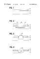
- FIG. 1is a side view of a semiconductor substrate with a first and a second insulation layers thereover.
- FIG. 2is a side view of the semiconductor substrate of FIG. 1 with the first and second insulation layers patterned by means of a photoresist mask.
- FIG. 3is a side view of the semiconductor substrate of FIG. 2 after an anisotropic etch step.
- FIG. 4is a side view of the substrate of FIG. 3 after an etching undercut step and an ion implantation step.
- FIG. 5is a side view of the device of FIG. 4 after an oxidation step.
- FIG. 6is a side view of the device of FIG. 5 after a trench-filling step.
- FIG. 7is a side view of the device of FIG. 6 after the removal of the first and second insulation layers and the deposit of a tunnel oxide layer and a polysilicon layer thereover.
- a semiconductor substrate 10which, in an exemplary embodiment, comprises a silicon substrate.
- this silicon substrate 10may be single crystal P-type silicon with an orientation which is most likely [100].
- a thin layer of insulator 12is formed over the silicon substrate 10 .
- This insulator layer 12may conveniently comprise a thermally grown SiO 2 and is typically referred to as a pad oxide layer.
- This pad oxide layer 12may be thermally grown typically to a thickness on the order of 250 ⁇ .
- Formed over the insulator layer 12is a second different insulator layer to function as an oxidation mask.
- the second different insulator layer 14may comprise a silicon nitride layer formed by means of a CVD process to a thickness typically in the range of 1700 ⁇ .
- the semiconductor device of FIG. 1is shown with a patterned photo-resist layer 16 formed thereon.
- the resist patternis used to protect the areas where active devices will be formed.
- This patterning of the resistmay be accomplished by means of standard photolithograph and etching techniques which are well-known in the art.
- the photolithography processwould typically involve selectively exposing the photo-resist layer to UV radiation and then processing the photo-resist layer to remove those sections which were exposed to the UV radiation.
- the silicon nitride layer 14 and the pad oxide layer 12may then be etched using appropriate standard dry etching solutions.
- the semiconductor device of FIG. 2is shown after the formation of a trench region 20 .
- the trench 20is formed by means of an anisotopric directional etch applied to the area not covered by the patterned mesas of pad oxide 12 and nitride 14 . Because a directional etch is utilized, the sidewalls of the resulting trench 20 are substantially vertical. By way of example this directional etch is typically performed to a depth of 3,000 ⁇ to 4,000 ⁇ .
- FIG. 4the semiconductor device of FIG. 3 is shown after the performance of an etch process to remove a lateral portion of the pad oxide layer 12 and, in a preferred embodiment, to implant material in this exposed corner of silicon which will reduce oxidation encroachment during subsequent oxidation steps.
- an etch process stepis applied to the semiconductor device to remove a lateral portion of the pad oxide layer 12 which is exposed at the sidewalls of the trench 20 to thereby undercut the second insulator layer of nitride 14 at its sidewall edges.
- this lateral etching stepmay etch approximately 100 ⁇ into the first insulator layer 12 of oxide.
- any etching processmay be utilized which selectively etches the first insulator layer 12 but does not etch the second insulator layer 14 or the silicon substrate 10 therebelow.
- the etch processmay comprise the use of a dilute HF dip (1:100 solution) to remove part of the oxide pad 12 to yield a slow controlled etch.
- this material implanted or insertedis for the purpose of controlling and reducing the oxidation rate of the silicon at the point of the implant.
- nitrogenmay be implanted in order to effect this oxidation rate control on the newly exposed silicon surfaces 24 .
- this implantation stepmay be accomplished by directing low energy N atoms and molecules at an angle in the range of 45°-60° from vertical with an energy of approximately 10-20 KEV to achieve a dosage of about 1E14-5E14.
- the semiconductor device of FIG. 4is shown after an oxidation step to grow a layer of oxide 26 on the sidewalls of the trench 20 .
- the purpose of this oxidation stepis to grow oxide 28 into the damaged corners of silicon by a controlled amount.
- the oxidemay be grown at a temperature in the range of 1000° C. for forty minutes to approximately 1 hour. If a material implant is utilized in the corners 24 , as described in the preferred embodiment, then this oxide formation at the damaged corners 28 will be on the order of 400-500 ⁇ .
- this trench 24may be filled with a CVD oxide.
- the semiconductor devicemay be polished to planarize the surface, to the form shown in FIG. 6 .
- this polishing stepmay be accomplished by means of chemical-mechanical polishing.
- Chemical-mechanical (CMP) polishing processesemploy both a chemical and a mechanical component. A rotating or vibrating disk or pad is moved relative to the semiconductor wafer surface in the presence of a chemical-mechanical polishing slurry. This CMP slurry includes suspended solids as well as a chemical solution component which attacks the material being polished.
- the semiconductor device of FIG. 6is shown after a tunnel oxide deposition step and the deposition of a layer of polysilicon.
- the nitride layer 14is removed with a wet etch that is selective to nitride and the pad oxide layer is removed with an etch such as, for example, a HF etch.
- the removal of the nitride layer and the pad oxide layerexposes silicon in the silicon substrate 10 where the transistor devices are to be formed.
- a thin layer of sacrificial oxide on the order of about 200 ⁇is grown followed by a sacrificial oxide removal step.
- a layer 32 of tunnel oxideis thermally grown on the surface of the silicon.
- a conductive polysilicon layer 34is deposited thereover, by way of example, by a CVD process.
- This polysilicon layermay be amorphous polysilicon and may include doping, or doping may be added after deposition to provide a desired conductivity.
- a typical doping concentration for this polysilicon layer 34which is set forth by way of example, and not by way of limitation, is phosphorus at 5E19 per cm 3 .
- This polysilicon layer 34typically will be deposited to a thickness on the order of 700-1100 ⁇ .
- a semiconductor deviceis formed wherein the active regions in the tunnel oxide area are prevented from extending into the damaged area of silicon by the oxide growth regions 28 .
- this processavoids and the resulting device avoids data retention problems caused by electron leakage through defect sites and further avoids substantial electron tunneling through defect sites that may cause tunnel oxide breakdown and shorting.
Landscapes
- Engineering & Computer Science (AREA)
- Physics & Mathematics (AREA)
- Condensed Matter Physics & Semiconductors (AREA)
- General Physics & Mathematics (AREA)
- Manufacturing & Machinery (AREA)
- Computer Hardware Design (AREA)
- Microelectronics & Electronic Packaging (AREA)
- Power Engineering (AREA)
- Element Separation (AREA)
Abstract
Description
Claims (7)
Priority Applications (1)
| Application Number | Priority Date | Filing Date | Title |
|---|---|---|---|
| US09/440,934US6309949B1 (en) | 1997-12-12 | 1999-11-16 | Semiconductor isolation process to minimize weak oxide problems |
Applications Claiming Priority (2)
| Application Number | Priority Date | Filing Date | Title |
|---|---|---|---|
| US08/989,820US6002160A (en) | 1997-12-12 | 1997-12-12 | Semiconductor isolation process to minimize weak oxide problems |
| US09/440,934US6309949B1 (en) | 1997-12-12 | 1999-11-16 | Semiconductor isolation process to minimize weak oxide problems |
Related Parent Applications (1)
| Application Number | Title | Priority Date | Filing Date |
|---|---|---|---|
| US08/989,820DivisionUS6002160A (en) | 1997-12-12 | 1997-12-12 | Semiconductor isolation process to minimize weak oxide problems |
Publications (1)
| Publication Number | Publication Date |
|---|---|
| US6309949B1true US6309949B1 (en) | 2001-10-30 |
Family
ID=25535491
Family Applications (2)
| Application Number | Title | Priority Date | Filing Date |
|---|---|---|---|
| US08/989,820Expired - LifetimeUS6002160A (en) | 1997-12-12 | 1997-12-12 | Semiconductor isolation process to minimize weak oxide problems |
| US09/440,934Expired - LifetimeUS6309949B1 (en) | 1997-12-12 | 1999-11-16 | Semiconductor isolation process to minimize weak oxide problems |
Family Applications Before (1)
| Application Number | Title | Priority Date | Filing Date |
|---|---|---|---|
| US08/989,820Expired - LifetimeUS6002160A (en) | 1997-12-12 | 1997-12-12 | Semiconductor isolation process to minimize weak oxide problems |
Country Status (1)
| Country | Link |
|---|---|
| US (2) | US6002160A (en) |
Cited By (7)
| Publication number | Priority date | Publication date | Assignee | Title |
|---|---|---|---|---|
| US20030022459A1 (en)* | 1998-09-03 | 2003-01-30 | Dickerson David L. | Isolation region forming methods |
| US20030190773A1 (en)* | 2002-04-05 | 2003-10-09 | Nec Electronics Corporation | Method for manufacturing semiconductor device using shallow trench isolation process |
| US20040077152A1 (en)* | 1999-06-01 | 2004-04-22 | Norio Ishitsuka | Process for producing semiconductor device and semiconductor device produced thereby |
| KR100466188B1 (en)* | 2002-05-29 | 2005-01-13 | 주식회사 하이닉스반도체 | Method of manufacturing for floating gate in flash memory cell |
| US20050009292A1 (en)* | 2003-07-09 | 2005-01-13 | Myung Gyu Choi | Method for forming isolation layer of semiconductor device |
| US20050208730A1 (en)* | 1998-09-03 | 2005-09-22 | Moore John T | Methods of forming materials within openings, and methods of forming isolation regions |
| CN107026192A (en)* | 2016-02-02 | 2017-08-08 | 中芯国际集成电路制造(上海)有限公司 | The manufacture method of semiconductor device |
Families Citing this family (11)
| Publication number | Priority date | Publication date | Assignee | Title |
|---|---|---|---|---|
| US7235856B1 (en)* | 1997-12-18 | 2007-06-26 | Micron Technology, Inc. | Trench isolation for semiconductor devices |
| US6169011B1 (en)* | 1998-03-24 | 2001-01-02 | Sharp Laboratories Of America, Inc. | Trench isolation structure and method for same |
| US6238998B1 (en) | 1998-11-20 | 2001-05-29 | International Business Machines Corporation | Shallow trench isolation on a silicon substrate using nitrogen implant into the side wall |
| JP4649006B2 (en)* | 1999-07-16 | 2011-03-09 | ルネサスエレクトロニクス株式会社 | Semiconductor device |
| US6150670A (en)* | 1999-11-30 | 2000-11-21 | International Business Machines Corporation | Process for fabricating a uniform gate oxide of a vertical transistor |
| US6388305B1 (en)* | 1999-12-17 | 2002-05-14 | International Business Machines Corporation | Electrically programmable antifuses and methods for forming the same |
| WO2002023624A2 (en)* | 2000-09-14 | 2002-03-21 | Infineon Technologies North America Corp. | Field effect transistor and method of fabrication |
| US6521510B1 (en)* | 2001-03-23 | 2003-02-18 | Advanced Micro Devices, Inc. | Method for shallow trench isolation with removal of strained island edges |
| US6635537B2 (en)* | 2001-04-06 | 2003-10-21 | United Microelectronics Corp. | Method of fabricating gate oxide |
| US20060240660A1 (en)* | 2005-04-20 | 2006-10-26 | Jin-Sheng Yang | Semiconductor stucture and method of manufacturing the same |
| FR3103628A1 (en)* | 2019-11-22 | 2021-05-28 | Stmicroelectronics (Crolles 2) Sas | Manufacturing process of an electronic device |
Citations (16)
| Publication number | Priority date | Publication date | Assignee | Title |
|---|---|---|---|---|
| US4576834A (en)* | 1985-05-20 | 1986-03-18 | Ncr Corporation | Method for forming trench isolation structures |
| US4580330A (en)* | 1984-06-15 | 1986-04-08 | Texas Instruments Incorporated | Integrated circuit isolation |
| US4944836A (en) | 1985-10-28 | 1990-07-31 | International Business Machines Corporation | Chem-mech polishing method for producing coplanar metal/insulator films on a substrate |
| US5084071A (en) | 1989-03-07 | 1992-01-28 | International Business Machines Corporation | Method of chemical-mechanical polishing an electronic component substrate and polishing slurry therefor |
| US5372950A (en)* | 1991-05-18 | 1994-12-13 | Samsung Electronics Co., Ltd. | Method for forming isolation regions in a semiconductor memory device |
| US5410176A (en) | 1991-04-05 | 1995-04-25 | Sgs-Thomson Microelectronics, Inc. | Integrated circuit with planarized shallow trench isolation |
| US5492858A (en)* | 1994-04-20 | 1996-02-20 | Digital Equipment Corporation | Shallow trench isolation process for high aspect ratio trenches |
| US5498891A (en) | 1990-12-20 | 1996-03-12 | Fujitsu Limited | EPROM with trench in thick field oxide |
| US5668403A (en) | 1994-07-29 | 1997-09-16 | Mitsubishi Denki Kabushiki Kaisha | Semiconductor device with reduced leakage current |
| US5767000A (en)* | 1996-06-05 | 1998-06-16 | Advanced Micro Devices, Inc. | Method of manufacturing subfield conductive layer |
| US5858866A (en)* | 1996-11-22 | 1999-01-12 | International Business Machines Corportation | Geometrical control of device corner threshold |
| US5863827A (en)* | 1997-06-03 | 1999-01-26 | Texas Instruments Incorporated | Oxide deglaze before sidewall oxidation of mesa or trench |
| US5891787A (en)* | 1997-09-04 | 1999-04-06 | Advanced Micro Devices, Inc. | Semiconductor fabrication employing implantation of excess atoms at the edges of a trench isolation structure |
| US5937308A (en)* | 1997-03-26 | 1999-08-10 | Advanced Micro Devices, Inc. | Semiconductor trench isolation structure formed substantially within a single chamber |
| US5985735A (en)* | 1995-09-29 | 1999-11-16 | Intel Corporation | Trench isolation process using nitrogen preconditioning to reduce crystal defects |
| US6008107A (en)* | 1990-06-14 | 1999-12-28 | National Semiconductor Corporation | Method of planarizing integrated circuits with fully recessed isolation dielectric |
- 1997
- 1997-12-12USUS08/989,820patent/US6002160A/ennot_activeExpired - Lifetime
- 1999
- 1999-11-16USUS09/440,934patent/US6309949B1/ennot_activeExpired - Lifetime
Patent Citations (16)
| Publication number | Priority date | Publication date | Assignee | Title |
|---|---|---|---|---|
| US4580330A (en)* | 1984-06-15 | 1986-04-08 | Texas Instruments Incorporated | Integrated circuit isolation |
| US4576834A (en)* | 1985-05-20 | 1986-03-18 | Ncr Corporation | Method for forming trench isolation structures |
| US4944836A (en) | 1985-10-28 | 1990-07-31 | International Business Machines Corporation | Chem-mech polishing method for producing coplanar metal/insulator films on a substrate |
| US5084071A (en) | 1989-03-07 | 1992-01-28 | International Business Machines Corporation | Method of chemical-mechanical polishing an electronic component substrate and polishing slurry therefor |
| US6008107A (en)* | 1990-06-14 | 1999-12-28 | National Semiconductor Corporation | Method of planarizing integrated circuits with fully recessed isolation dielectric |
| US5498891A (en) | 1990-12-20 | 1996-03-12 | Fujitsu Limited | EPROM with trench in thick field oxide |
| US5410176A (en) | 1991-04-05 | 1995-04-25 | Sgs-Thomson Microelectronics, Inc. | Integrated circuit with planarized shallow trench isolation |
| US5372950A (en)* | 1991-05-18 | 1994-12-13 | Samsung Electronics Co., Ltd. | Method for forming isolation regions in a semiconductor memory device |
| US5492858A (en)* | 1994-04-20 | 1996-02-20 | Digital Equipment Corporation | Shallow trench isolation process for high aspect ratio trenches |
| US5668403A (en) | 1994-07-29 | 1997-09-16 | Mitsubishi Denki Kabushiki Kaisha | Semiconductor device with reduced leakage current |
| US5985735A (en)* | 1995-09-29 | 1999-11-16 | Intel Corporation | Trench isolation process using nitrogen preconditioning to reduce crystal defects |
| US5767000A (en)* | 1996-06-05 | 1998-06-16 | Advanced Micro Devices, Inc. | Method of manufacturing subfield conductive layer |
| US5858866A (en)* | 1996-11-22 | 1999-01-12 | International Business Machines Corportation | Geometrical control of device corner threshold |
| US5937308A (en)* | 1997-03-26 | 1999-08-10 | Advanced Micro Devices, Inc. | Semiconductor trench isolation structure formed substantially within a single chamber |
| US5863827A (en)* | 1997-06-03 | 1999-01-26 | Texas Instruments Incorporated | Oxide deglaze before sidewall oxidation of mesa or trench |
| US5891787A (en)* | 1997-09-04 | 1999-04-06 | Advanced Micro Devices, Inc. | Semiconductor fabrication employing implantation of excess atoms at the edges of a trench isolation structure |
Cited By (12)
| Publication number | Priority date | Publication date | Assignee | Title |
|---|---|---|---|---|
| US20030022459A1 (en)* | 1998-09-03 | 2003-01-30 | Dickerson David L. | Isolation region forming methods |
| US20050208730A1 (en)* | 1998-09-03 | 2005-09-22 | Moore John T | Methods of forming materials within openings, and methods of forming isolation regions |
| US20060234469A1 (en)* | 1998-09-03 | 2006-10-19 | Micron Technology, Inc. | A method of forming semiconductor structures |
| US7358587B2 (en) | 1998-09-03 | 2008-04-15 | Micron Technology, Inc. | Semiconductor structures |
| US20040077152A1 (en)* | 1999-06-01 | 2004-04-22 | Norio Ishitsuka | Process for producing semiconductor device and semiconductor device produced thereby |
| US6858515B2 (en)* | 1999-06-01 | 2005-02-22 | Renesas Technology Corp. | Process for producing semiconductor device and semiconductor device produced thereby |
| US20030190773A1 (en)* | 2002-04-05 | 2003-10-09 | Nec Electronics Corporation | Method for manufacturing semiconductor device using shallow trench isolation process |
| KR100466188B1 (en)* | 2002-05-29 | 2005-01-13 | 주식회사 하이닉스반도체 | Method of manufacturing for floating gate in flash memory cell |
| US20050009292A1 (en)* | 2003-07-09 | 2005-01-13 | Myung Gyu Choi | Method for forming isolation layer of semiconductor device |
| US6921705B2 (en)* | 2003-07-09 | 2005-07-26 | Hynix Semiconductor Inc. | Method for forming isolation layer of semiconductor device |
| CN107026192A (en)* | 2016-02-02 | 2017-08-08 | 中芯国际集成电路制造(上海)有限公司 | The manufacture method of semiconductor device |
| CN107026192B (en)* | 2016-02-02 | 2020-05-29 | 中芯国际集成电路制造(上海)有限公司 | Method for manufacturing semiconductor device |
Also Published As
| Publication number | Publication date |
|---|---|
| US6002160A (en) | 1999-12-14 |
Similar Documents
| Publication | Publication Date | Title |
|---|---|---|
| US6309949B1 (en) | Semiconductor isolation process to minimize weak oxide problems | |
| KR100358630B1 (en) | Planar and densely patterned silicon-on-insulator structure and process of fabricating | |
| US6004862A (en) | Core array and periphery isolation technique | |
| KR100213196B1 (en) | Trench device separation | |
| US5270234A (en) | Deep submicron transistor fabrication method | |
| US6027998A (en) | Method for fully planarized conductive line for a stack gate | |
| KR960016502B1 (en) | Integrated circuit isolation method | |
| US5966614A (en) | Silicon nitride-free isolation methods for integrated circuits | |
| JPH04250650A (en) | Flattening of integrated circuit provided with completely recessed isolation insulator | |
| CN1204148A (en) | Integrated Circuit Devices with Shallow Trench Isolation | |
| JP2006502573A (en) | FIELD EFFECT TRANSISTOR HAVING SOURCE / Drain Partially Insulating Portion, | |
| WO1994014192A1 (en) | Thin soi layer for fully depleted field effect transistors | |
| EP0405923B1 (en) | Method for forming variable width isolation structures | |
| US5137843A (en) | Isolation method for semiconductor device | |
| US4950618A (en) | Masking scheme for silicon dioxide mesa formation | |
| US5849625A (en) | Planar field oxide isolation process for semiconductor integrated circuit devices using liquid phase deposition | |
| EP0293979A2 (en) | Zero bird-beak oxide isolation scheme for integrated circuits | |
| US6350659B1 (en) | Process of making semiconductor device having regions of insulating material formed in a semiconductor substrate | |
| KR100566305B1 (en) | Trench type isolation layer formation method of semiconductor device | |
| US7148117B2 (en) | Methods for forming shallow trench isolation structures in semiconductor devices | |
| US6261966B1 (en) | Method for improving trench isolation | |
| KR940006671B1 (en) | Manufacturing method of semiconductor device having soi structure | |
| KR101097011B1 (en) | Manufacturing Method of Semiconductor Device | |
| KR100312656B1 (en) | Method for fabricating bc-soi device | |
| KR0176151B1 (en) | Isolation method of semiconductor device |
Legal Events
| Date | Code | Title | Description |
|---|---|---|---|
| STCF | Information on status: patent grant | Free format text:PATENTED CASE | |
| FEPP | Fee payment procedure | Free format text:PAYOR NUMBER ASSIGNED (ORIGINAL EVENT CODE: ASPN); ENTITY STATUS OF PATENT OWNER: LARGE ENTITY | |
| FPAY | Fee payment | Year of fee payment:4 | |
| AS | Assignment | Owner name:SPANSION INC., CALIFORNIA Free format text:ASSIGNMENT OF ASSIGNORS INTEREST;ASSIGNOR:ADVANCED MICRO DEVICES, INC.;REEL/FRAME:019028/0623 Effective date:20070131 | |
| AS | Assignment | Owner name:SPANSION LLC, CALIFORNIA Free format text:ASSIGNMENT OF ASSIGNORS INTEREST;ASSIGNOR:SPANSION INC.;REEL/FRAME:019069/0028 Effective date:20070131 | |
| FPAY | Fee payment | Year of fee payment:8 | |
| AS | Assignment | Owner name:BARCLAYS BANK PLC,NEW YORK Free format text:SECURITY AGREEMENT;ASSIGNORS:SPANSION LLC;SPANSION INC.;SPANSION TECHNOLOGY INC.;AND OTHERS;REEL/FRAME:024522/0338 Effective date:20100510 Owner name:BARCLAYS BANK PLC, NEW YORK Free format text:SECURITY AGREEMENT;ASSIGNORS:SPANSION LLC;SPANSION INC.;SPANSION TECHNOLOGY INC.;AND OTHERS;REEL/FRAME:024522/0338 Effective date:20100510 | |
| FPAY | Fee payment | Year of fee payment:12 | |
| AS | Assignment | Owner name:SPANSION TECHNOLOGY LLC, CALIFORNIA Free format text:RELEASE BY SECURED PARTY;ASSIGNOR:BARCLAYS BANK PLC;REEL/FRAME:035201/0159 Effective date:20150312 Owner name:SPANSION INC., CALIFORNIA Free format text:RELEASE BY SECURED PARTY;ASSIGNOR:BARCLAYS BANK PLC;REEL/FRAME:035201/0159 Effective date:20150312 Owner name:SPANSION LLC, CALIFORNIA Free format text:RELEASE BY SECURED PARTY;ASSIGNOR:BARCLAYS BANK PLC;REEL/FRAME:035201/0159 Effective date:20150312 | |
| AS | Assignment | Owner name:MORGAN STANLEY SENIOR FUNDING, INC., NEW YORK Free format text:SECURITY INTEREST;ASSIGNORS:CYPRESS SEMICONDUCTOR CORPORATION;SPANSION LLC;REEL/FRAME:035240/0429 Effective date:20150312 | |
| AS | Assignment | Owner name:CYPRESS SEMICONDUCTOR CORPORATION, CALIFORNIA Free format text:ASSIGNMENT OF ASSIGNORS INTEREST;ASSIGNOR:SPANSION, LLC;REEL/FRAME:036032/0154 Effective date:20150601 | |
| AS | Assignment | Owner name:CYPRESS SEMICONDUCTOR CORPORATION, CALIFORNIA Free format text:PARTIAL RELEASE OF SECURITY INTEREST IN PATENTS;ASSIGNOR:MORGAN STANLEY SENIOR FUNDING, INC., AS COLLATERAL AGENT;REEL/FRAME:039708/0001 Effective date:20160811 Owner name:SPANSION LLC, CALIFORNIA Free format text:PARTIAL RELEASE OF SECURITY INTEREST IN PATENTS;ASSIGNOR:MORGAN STANLEY SENIOR FUNDING, INC., AS COLLATERAL AGENT;REEL/FRAME:039708/0001 Effective date:20160811 | |
| AS | Assignment | Owner name:MONTEREY RESEARCH, LLC, CALIFORNIA Free format text:ASSIGNMENT OF ASSIGNORS INTEREST;ASSIGNOR:CYPRESS SEMICONDUCTOR CORPORATION;REEL/FRAME:040911/0238 Effective date:20160811 | |
| AS | Assignment | Owner name:MORGAN STANLEY SENIOR FUNDING, INC., NEW YORK Free format text:CORRECTIVE ASSIGNMENT TO CORRECT THE 8647899 PREVIOUSLY RECORDED ON REEL 035240 FRAME 0429. ASSIGNOR(S) HEREBY CONFIRMS THE SECURITY INTERST;ASSIGNORS:CYPRESS SEMICONDUCTOR CORPORATION;SPANSION LLC;REEL/FRAME:058002/0470 Effective date:20150312 |