US6309918B1 - Manufacturable GaAs VFET process - Google Patents
Manufacturable GaAs VFET processDownload PDFInfo
- Publication number
- US6309918B1 US6309918B1US09/157,430US15743098AUS6309918B1US 6309918 B1US6309918 B1US 6309918B1US 15743098 AUS15743098 AUS 15743098AUS 6309918 B1US6309918 B1US 6309918B1
- Authority
- US
- United States
- Prior art keywords
- gate
- layer
- areas
- gaas
- depositing
- Prior art date
- Legal status (The legal status is an assumption and is not a legal conclusion. Google has not performed a legal analysis and makes no representation as to the accuracy of the status listed.)
- Expired - Fee Related
Links
- 229910001218Gallium arsenideInorganic materials0.000titleclaimsabstractdescription58
- 238000000034methodMethods0.000titleclaimsabstractdescription49
- 239000000758substrateSubstances0.000claimsabstractdescription37
- 238000004891communicationMethods0.000claimsabstractdescription10
- 229910052751metalInorganic materials0.000claimsdescription32
- 239000002184metalSubstances0.000claimsdescription32
- 238000000151depositionMethods0.000claimsdescription26
- 238000005530etchingMethods0.000claimsdescription14
- 239000000463materialSubstances0.000claimsdescription14
- 239000004020conductorSubstances0.000claimsdescription12
- 239000007943implantSubstances0.000claimsdescription12
- 229920002120photoresistant polymerPolymers0.000claimsdescription12
- 238000000137annealingMethods0.000claimsdescription8
- XKRFYHLGVUSROY-UHFFFAOYSA-NArgonChemical compound[Ar]XKRFYHLGVUSROY-UHFFFAOYSA-N0.000claimsdescription6
- 230000004913activationEffects0.000claimsdescription6
- ZAMOUSCENKQFHK-UHFFFAOYSA-NChlorine atomChemical compound[Cl]ZAMOUSCENKQFHK-UHFFFAOYSA-N0.000claimsdescription5
- 239000000460chlorineSubstances0.000claimsdescription5
- 229910052801chlorineInorganic materials0.000claimsdescription5
- 239000003870refractory metalSubstances0.000claimsdescription4
- 229910000530Gallium indium arsenideInorganic materials0.000claimsdescription3
- 229910052786argonInorganic materials0.000claimsdescription3
- 229910052799carbonInorganic materials0.000claimsdescription3
- -1carbon ionsChemical class0.000claimsdescription3
- 229910044991metal oxideInorganic materials0.000claimsdescription3
- 150000004706metal oxidesChemical class0.000claimsdescription3
- 150000004767nitridesChemical class0.000claimsdescription3
- 238000000059patterningMethods0.000claimsdescription3
- 229910021332silicideInorganic materials0.000claimsdescription3
- 239000011810insulating materialSubstances0.000claims2
- FVBUAEGBCNSCDD-UHFFFAOYSA-Nsilicide(4-)Chemical compound[Si-4]FVBUAEGBCNSCDD-UHFFFAOYSA-N0.000claims2
- 230000003213activating effectEffects0.000claims1
- 238000001020plasma etchingMethods0.000claims1
- 229910004205SiNXInorganic materials0.000description4
- 238000002513implantationMethods0.000description4
- BOTDANWDWHJENH-UHFFFAOYSA-NTetraethyl orthosilicateChemical compoundCCO[Si](OCC)(OCC)OCCBOTDANWDWHJENH-UHFFFAOYSA-N0.000description3
- 239000010931goldSubstances0.000description3
- 238000001459lithographyMethods0.000description3
- VYPSYNLAJGMNEJ-UHFFFAOYSA-NSilicium dioxideChemical compoundO=[Si]=OVYPSYNLAJGMNEJ-UHFFFAOYSA-N0.000description2
- 229910045601alloyInorganic materials0.000description2
- 239000000956alloySubstances0.000description2
- 230000008021depositionEffects0.000description2
- 230000008020evaporationEffects0.000description2
- 238000001704evaporationMethods0.000description2
- 230000005669field effectEffects0.000description2
- PCHJSUWPFVWCPO-UHFFFAOYSA-NgoldChemical compound[Au]PCHJSUWPFVWCPO-UHFFFAOYSA-N0.000description2
- 229910052737goldInorganic materials0.000description2
- 238000012986modificationMethods0.000description2
- 230000004048modificationEffects0.000description2
- 238000012545processingMethods0.000description2
- 125000006850spacer groupChemical group0.000description2
- 238000004544sputter depositionMethods0.000description2
- 238000012360testing methodMethods0.000description2
- 229910015844BCl3Inorganic materials0.000description1
- KZBUYRJDOAKODT-UHFFFAOYSA-NChlorineChemical compoundClClKZBUYRJDOAKODT-UHFFFAOYSA-N0.000description1
- PXGOKWXKJXAPGV-UHFFFAOYSA-NFluorineChemical compoundFFPXGOKWXKJXAPGV-UHFFFAOYSA-N0.000description1
- 230000005540biological transmissionEffects0.000description1
- 230000015572biosynthetic processEffects0.000description1
- 229910052681coesiteInorganic materials0.000description1
- 229910052906cristobaliteInorganic materials0.000description1
- 230000000593degrading effectEffects0.000description1
- 229910052731fluorineInorganic materials0.000description1
- 239000011737fluorineSubstances0.000description1
- 238000010348incorporationMethods0.000description1
- 150000002500ionsChemical class0.000description1
- 238000004519manufacturing processMethods0.000description1
- 230000000873masking effectEffects0.000description1
- 238000005259measurementMethods0.000description1
- 150000002739metalsChemical class0.000description1
- 238000000206photolithographyMethods0.000description1
- 230000000717retained effectEffects0.000description1
- 239000004065semiconductorSubstances0.000description1
- 239000000377silicon dioxideSubstances0.000description1
- 229910052682stishoviteInorganic materials0.000description1
- FAQYAMRNWDIXMY-UHFFFAOYSA-NtrichloroboraneChemical compoundClB(Cl)ClFAQYAMRNWDIXMY-UHFFFAOYSA-N0.000description1
- 229910052905tridymiteInorganic materials0.000description1
- WQJQOUPTWCFRMM-UHFFFAOYSA-Ntungsten disilicideChemical compound[Si]#[W]#[Si]WQJQOUPTWCFRMM-UHFFFAOYSA-N0.000description1
- 229910021342tungsten silicideInorganic materials0.000description1
Images


Classifications
- H—ELECTRICITY
- H10—SEMICONDUCTOR DEVICES; ELECTRIC SOLID-STATE DEVICES NOT OTHERWISE PROVIDED FOR
- H10D—INORGANIC ELECTRIC SEMICONDUCTOR DEVICES
- H10D30/00—Field-effect transistors [FET]
- H10D30/01—Manufacture or treatment
- H10D30/061—Manufacture or treatment of FETs having Schottky gates
- H—ELECTRICITY
- H10—SEMICONDUCTOR DEVICES; ELECTRIC SOLID-STATE DEVICES NOT OTHERWISE PROVIDED FOR
- H10D—INORGANIC ELECTRIC SEMICONDUCTOR DEVICES
- H10D30/00—Field-effect transistors [FET]
- H10D30/80—FETs having rectifying junction gate electrodes
- H10D30/87—FETs having Schottky gate electrodes, e.g. metal-semiconductor FETs [MESFET]
- H10D30/871—Vertical FETs having Schottky gate electrodes
- Y—GENERAL TAGGING OF NEW TECHNOLOGICAL DEVELOPMENTS; GENERAL TAGGING OF CROSS-SECTIONAL TECHNOLOGIES SPANNING OVER SEVERAL SECTIONS OF THE IPC; TECHNICAL SUBJECTS COVERED BY FORMER USPC CROSS-REFERENCE ART COLLECTIONS [XRACs] AND DIGESTS
- Y10—TECHNICAL SUBJECTS COVERED BY FORMER USPC
- Y10S—TECHNICAL SUBJECTS COVERED BY FORMER USPC CROSS-REFERENCE ART COLLECTIONS [XRACs] AND DIGESTS
- Y10S438/00—Semiconductor device manufacturing: process
- Y10S438/942—Masking
- Y10S438/945—Special, e.g. metal
Definitions
- the present inventionpertains to a process for fabricating GaAs vertical field effect transistors (VFET) and more specifically to a manufacturable GaAs VFET process.
- VFETvertical field effect transistors
- VFETsvertical field effect transistors
- the doped areas or implanted areasmust then be activated by a relatively high annealing temperature.
- the annealing temperatureis high enough to cause major problems with any ohmic metal that has been previously deposited on the substrate. For example, most of the ohmic metals contain gold and annealing temperatures will cause gold to diffuse into the substrate and produce a very bad ohmic contact.
- a manufacturable GaAs VFET processincluding providing a substrate structure with a doped GaAs supporting substrate, a lightly doped first epitaxial layer including GaAs positioned on a first surface of the supporting substrate, and a heavily doped second epitaxial layer including GaAs positioned on the first epitaxial layer.
- a temperature tolerant conductive layeris positioned on the second epitaxial layer and patterned to define a plurality of source areas underlying the patterned portions of the conductive layer.
- the portions of patterned conductive layerare used as a mask and a plurality of gate trenches are etched through the second epitaxial layer and into the first epitaxial layer of the substrate structure adjacent the source areas.
- the bottoms of the gate trenchesare spaced vertically from the second epitaxial layer.
- Materialis implanted in the bottoms of the gate trenches to form implanted gate areas in the gate trenches and the implanted gate areas are activated by annealing.
- a gate contactis formed in communication with the implanted gate areas, a source contact is formed in communication with the portions of patterned conductive layer overlying the source areas, and a drain contact is formed on the rear surface of the substrate structure.
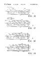
- FIG. 1 through FIG. 18are sectional views illustrating various sequential steps in a manufacturable GaAs VFET process in accordance with the present invention.
- FIG. 19is a sectional view of a GaAs VFET fabricated in accordance with the process illustrated.
- FIG. 1illustrates a substrate structure 10 including a doped GaAs supporting substrate 11 , a lightly doped first epitaxial layer 12 positioned on a first surface 13 of supporting substrate 11 , and a heavily doped second epitaxial layer 15 positioned on first epitaxial layer 12 .
- substrate structure 10could include more or less layers depending upon the specific application.
- supporting substrate 11is formed of GaAs which is doped n+
- first epitaxial layer 12is formed of GaAs which is lightly doped n ⁇
- second epitaxial layer 15is heavily doped n++ In GaAs.
- a temperature tolerant conductive layer 17is deposited, generally by sputtering, on second epitaxial layer 15 .
- Layer 17has a thickness in a range of approximately 2000 ⁇ to approximately 8000 ⁇ .
- second epitaxial layer 15is heavily doped n++ In GaAs, due to the narrow band gap of the InGaAs, practically any metal forms a good ohmic contact to second epitaxial layer 15 .
- many conductive materialswhen deposited on a semiconductor material such as second epitaxial layer 15 , will diffuse into the underlying layer during subsequent process steps, such as annealing and other high temperature processes. This mixing of the materials between the layers produces a very poor electrical contact.
- Temperature tolerant conductive layer 17can include, for example, one or a combination of refractory metals, metal silicides, metal nitrides, metal oxides or the like. In a specific example, temperature tolerant conductive layer 17 includes approximately 3 k ⁇ of TiW, WSi x , tungsten silicide, or the like with an optional etch mask of 1.5 k ⁇ of SiN x .
- a layer 18 approximately 1 ⁇ m thick of photoresist materialis deposited on the surface of temperature tolerant conductive layer 17 .
- Layer 18is patterned to define a plurality of source areas 20 , as illustrated in FIG. 3. A larger area is utilized as a termination area 21 between the source and gate terminals, as will be apparent presently.
- the optional etch mask in temperature tolerant conductive layer 17aids in preventing damage to the conductive materials during patterning of layer 18 and is used in further processing, as will be described presently. Patterned layer 18 is then used as a mask in the etching of temperature tolerant conductive layer 17 , as illustrated in FIG. 4 .
- conventional positive stepper lithographycan be used to define the areas 20 and 21 and reactive ion etch (RIE) can be used to etch away layer 17 down to second epitaxial layer 15 in the exposed areas.
- RIEreactive ion etch
- CD measurements of the patterncan be taken during this step to determine the source dimensions and the gate length.
- the remaining photoresistcan be stripped, as illustrated in FIG. 5 or it can optionally be retained for additional protection in the following steps.
- gate trenches 25extend through second epitaxial layer 15 and into first epitaxial layer 12 to separate second epitaxial layer 15 into source areas 20 positioned beneath and in electrical contact with elongated fingers of temperature tolerant conductive layer 17 .
- Gate trenches 25extend through second epitaxial layer 15 and into first epitaxial layer 12 sufficiently to prevent shorting between the source and gate, as will be understood presently.
- chlorine based etchese.g. chlorine chemistries such as BCl 3 +Cl 2 , etc.
- the photoresist used to pattern layer 17can remain as a mask for the etching of gate trenches 25 .
- a sacrificial etch mask of SiN x (described above) or other dielectric hard maskis blanket deposited following the temperature tolerant conductive material in layer 17 and patterned simultaneously with the layer 17 photoresist and etch procedure.
- the temperature tolerant conductive material in layer 17is used directly as an etch mask, given a sufficient etch rate selectivity between layer 17 and layers 15 and 12 .
- Gate trenches 25are formed with bottoms 26 spaced from second epitaxial layer 15 by substantially vertical sides.
- gate areas 30are implanted in bottoms 26 of gate trenches 25 to form implanted gate areas 30 in the gate trenches and a gate contact area 31 on an opposite side of termination area 21 , as illustrated in FIG. 7 .
- all of gate trenches 25are physically and electrically connected together at one or both ends thereof and are further physically and electrically connected to gate contact area 31 by the same means.
- the same mask that was used to etch first and second epitaxial layers 12 and 15can be used as a mask during the implantation of gate areas 30 .
- gate areas 30are p-type conductivity formed by the implantation of argon and carbon ions or other p-type species for GaAs material.
- the masking layers(whichever option is used) are tailored for the proper thickness to mask any given implant.
- a brief sidewall etchis performed on trenches 25 to remove any potential leakage paths.
- the brief sidewall etch or cleanincludes an isotropic plasma or wet etch plus the optional removal of any remaining portions of the sacrificial etch mask of SiN x .
- dielectric sidewall spacerscould be formed before the implant step and removed subsequent to the implant step.
- some undercutting of source areas 20could be allowed during the etching of trenches 25 and/or during the brief sidewall etch.
- a very thin layer of gate metal or other conductive material(incorporated into gate areas 30 ) is optionally deposited, subsequent to the anneal step, on bottoms 26 of trenches 25 to improve the electrical conductance to gate contact area 31 .
- the undercutting(or dielectric sidewall spacers) ensure that this thin layer will not form leakage paths on the sidewalls of trenches 25 to source areas 20 .
- photoresist 35is deposited on the structure and patterned in any conventional manner to expose gate contact area 31 .
- Ohmic metal 36which in this specific embodiment is p-type ohmic metal, is deposited by evaporation in a well known manner as illustrated in FIG. 9 so as to contact implanted areas directly.
- a conventional lift-off techniqueis then used to remove all unwanted metal, as illustrated in FIG. 10 and a standard ohmic contact alloy is performed.
- the device or devices being fabricatedcan be probed (tested) for several characteristics so that further processing can be terminated in the event of poor or catastrophic characteristics. For example, n and p transmission line model (TLM) measures can be made to determine implant resistivity. Also, gate to source characteristics can be measured and possibly the three terminal functionality of the device or devices can be determined.
- TLMtransmission line model
- a suitable dielectric with good step coverage and planarizing attributesis deposited in a blanket layer 40 over the structure.
- tetraethylorthosilicateTEOS
- a top side planarizing processsuch as chemical-mechanical polish (CMP)
- CMPchemical-mechanical polish
- Planarized blanket layer 40is then patterned, for example with photoresist etch mask 41 , to define a source contact area 42 , as illustrated in FIG. 13 .
- the exposed portion or portions of blanket layer 40e.g.
- source contact area 42are then etched with a convenient isotropic etchant to open the entire area above the elongated fingers of temperature tolerant conductive layer 17 overlying source areas 20 , as illustrated in FIG. 14.
- a selective plasma etch, dielectric to source metal,is used to etch down to the tops of the elongated fingers of temperature tolerant conductive layer 17 .
- an isotropic SF 6 with an optional SiN x etchis used.
- photoresist etch mask 41is removed, as illustrated in FIG. 15, and a new liftoff photoresist layer 45 is deposited and patterned to redefine source contact area 42 to partially overlie termination area 21 , as illustrated in FIG. 16 .
- Bond pad metal 46e.g. Ti/Au or the like, is then selectively evaporated onto the elongated fingers of temperature tolerant conductive layer 17 using conventional liftoff lithography, as illustrated in FIGS. 17 and 18.
- Bond pad metal 46should be deposited thick enough for wire bonding in most applications.
- Supporting substrate 11can then be thinned, by any conventional wafer thinning technique, to approximately 4 mils and a drain contact 47 is deposited, by evaporation, sputtering, or the like on a rear surface of the substrate structure 10 .
- Drain contact 47in this embodiment, is n-type metal such as NiGeAu alloy, or the like.
- FIG. 19illustrates a sectional view of a final VFET structure in accordance with the present invention.
- the new and improved manufacturable GaAs VFET processallows the use of ohmic contacts prior to implant and activation steps as well as the use of source metal as a self-aligned etch and implant mask. Further, because of the early formation of source and gate conductive areas, the new and improved manufacturable GaAs VFET process allows testing of the VFETs at intermediate points in the process, which can greatly reduce unnecessary process costs. More specifically, the robust ohmic contacts using refractory metal or the like allows for subsequent high temperature processes, such as implant activation.
- gate trenchescan be self-aligned to the source metal contacts using the source metal as the etch mask (since chlorine etch is used for GaAs trench etch while fluorine is used for refractory ohmic metal etch). Because of this self-aligned feature, deep submicron source contacts become possible with the present process, since it is almost impossible to align accurately and consistently deep submicron vias over submicron size source contacts. The deep submicron source contacts enables very low voltage operation for GaAs VFETs. Further, controlled undercuts in the gate trenches are possible so that a thin layer of ohmic metal can be deposited over the gate implants to substantially reduce gate resistance.
Landscapes
- Junction Field-Effect Transistors (AREA)
- Electrodes Of Semiconductors (AREA)
Abstract
Description
Claims (18)
Priority Applications (1)
| Application Number | Priority Date | Filing Date | Title |
|---|---|---|---|
| US09/157,430US6309918B1 (en) | 1998-09-21 | 1998-09-21 | Manufacturable GaAs VFET process |
Applications Claiming Priority (1)
| Application Number | Priority Date | Filing Date | Title |
|---|---|---|---|
| US09/157,430US6309918B1 (en) | 1998-09-21 | 1998-09-21 | Manufacturable GaAs VFET process |
Publications (1)
| Publication Number | Publication Date |
|---|---|
| US6309918B1true US6309918B1 (en) | 2001-10-30 |
Family
ID=22563683
Family Applications (1)
| Application Number | Title | Priority Date | Filing Date |
|---|---|---|---|
| US09/157,430Expired - Fee RelatedUS6309918B1 (en) | 1998-09-21 | 1998-09-21 | Manufacturable GaAs VFET process |
Country Status (1)
| Country | Link |
|---|---|
| US (1) | US6309918B1 (en) |
Cited By (50)
| Publication number | Priority date | Publication date | Assignee | Title |
|---|---|---|---|---|
| US20060226478A1 (en)* | 2005-03-29 | 2006-10-12 | Brar Berinder P S | Semiconductor device having a lateral channel and contacts on opposing surfaces thereof |
| US20060255360A1 (en)* | 2005-05-13 | 2006-11-16 | Brar Berinder P S | Semiconductor device having multiple lateral channels and method of forming the same |
| US20070045765A1 (en)* | 2005-08-25 | 2007-03-01 | Brar Berinder P | Semiconductor device having substrate-driven field-effect transistor and schottky diode and method of forming the same |
| US20070069286A1 (en)* | 2005-09-27 | 2007-03-29 | Brar Berinder P S | Semiconductor device having an interconnect with sloped walls and method of forming the same |
| US20070185754A1 (en)* | 2006-02-07 | 2007-08-09 | Sap Ag | Task responsibility system |
| US20070187717A1 (en)* | 2005-05-13 | 2007-08-16 | Coldwatt, Inc. | Semiconductor device having reduced on-resistance and method of forming the same |
| US7280026B2 (en) | 2002-04-18 | 2007-10-09 | Coldwatt, Inc. | Extended E matrix integrated magnetics (MIM) core |
| US7298118B2 (en) | 2005-02-23 | 2007-11-20 | Coldwatt, Inc. | Power converter employing a tapped inductor and integrated magnetics and method of operating the same |
| US20070298564A1 (en)* | 2006-06-21 | 2007-12-27 | Brar Berinder P S | Vertical Field-Effect Transistor and Method of Forming the Same |
| US7321283B2 (en) | 2004-08-19 | 2008-01-22 | Coldwatt, Inc. | Vertical winding structures for planar magnetic switched-mode power converters |
| US20080048173A1 (en)* | 2005-08-25 | 2008-02-28 | Sadaka Mariam G | Semiconductor Device Including a Lateral Field-Effect Transistor and Schottky Diode |
| US7385375B2 (en) | 2005-02-23 | 2008-06-10 | Coldwatt, Inc. | Control circuit for a depletion mode switch and method of operating the same |
| US7417875B2 (en) | 2005-02-08 | 2008-08-26 | Coldwatt, Inc. | Power converter employing integrated magnetics with a current multiplier rectifier and method of operating the same |
| US7427910B2 (en) | 2004-08-19 | 2008-09-23 | Coldwatt, Inc. | Winding structure for efficient switch-mode power converters |
| US7439556B2 (en) | 2005-03-29 | 2008-10-21 | Coldwatt, Inc. | Substrate driven field-effect transistor |
| US7541640B2 (en) | 2006-06-21 | 2009-06-02 | Flextronics International Usa, Inc. | Vertical field-effect transistor and method of forming the same |
| US7667986B2 (en) | 2006-12-01 | 2010-02-23 | Flextronics International Usa, Inc. | Power system with power converters having an adaptive controller |
| US7675759B2 (en) | 2006-12-01 | 2010-03-09 | Flextronics International Usa, Inc. | Power system with power converters having an adaptive controller |
| US7675758B2 (en) | 2006-12-01 | 2010-03-09 | Flextronics International Usa, Inc. | Power converter with an adaptive controller and method of operating the same |
| US7876191B2 (en) | 2005-02-23 | 2011-01-25 | Flextronics International Usa, Inc. | Power converter employing a tapped inductor and integrated magnetics and method of operating the same |
| US7889517B2 (en) | 2006-12-01 | 2011-02-15 | Flextronics International Usa, Inc. | Power system with power converters having an adaptive controller |
| US7906941B2 (en) | 2007-06-19 | 2011-03-15 | Flextronics International Usa, Inc. | System and method for estimating input power for a power processing circuit |
| US8125205B2 (en) | 2006-08-31 | 2012-02-28 | Flextronics International Usa, Inc. | Power converter employing regulators with a coupled inductor |
| US8415737B2 (en) | 2006-06-21 | 2013-04-09 | Flextronics International Usa, Inc. | Semiconductor device with a pillar region and method of forming the same |
| US8486741B2 (en)* | 2004-09-17 | 2013-07-16 | Stmicroelectronics S.R.L. | Process for etching trenches in an integrated optical device |
| US8502520B2 (en) | 2007-03-14 | 2013-08-06 | Flextronics International Usa, Inc | Isolated power converter |
| US8514593B2 (en) | 2009-06-17 | 2013-08-20 | Power Systems Technologies, Ltd. | Power converter employing a variable switching frequency and a magnetic device with a non-uniform gap |
| US8520414B2 (en) | 2009-01-19 | 2013-08-27 | Power Systems Technologies, Ltd. | Controller for a power converter |
| US8520420B2 (en) | 2009-12-18 | 2013-08-27 | Power Systems Technologies, Ltd. | Controller for modifying dead time between switches in a power converter |
| US8638578B2 (en) | 2009-08-14 | 2014-01-28 | Power System Technologies, Ltd. | Power converter including a charge pump employable in a power adapter |
| US8643222B2 (en) | 2009-06-17 | 2014-02-04 | Power Systems Technologies Ltd | Power adapter employing a power reducer |
| US8767418B2 (en) | 2010-03-17 | 2014-07-01 | Power Systems Technologies Ltd. | Control system for a power converter and method of operating the same |
| US8787043B2 (en) | 2010-01-22 | 2014-07-22 | Power Systems Technologies, Ltd. | Controller for a power converter and method of operating the same |
| US8792256B2 (en) | 2012-01-27 | 2014-07-29 | Power Systems Technologies Ltd. | Controller for a switch and method of operating the same |
| US8792257B2 (en) | 2011-03-25 | 2014-07-29 | Power Systems Technologies, Ltd. | Power converter with reduced power dissipation |
| US8976549B2 (en) | 2009-12-03 | 2015-03-10 | Power Systems Technologies, Ltd. | Startup circuit including first and second Schmitt triggers and power converter employing the same |
| US9019061B2 (en) | 2009-03-31 | 2015-04-28 | Power Systems Technologies, Ltd. | Magnetic device formed with U-shaped core pieces and power converter employing the same |
| US9077248B2 (en) | 2009-06-17 | 2015-07-07 | Power Systems Technologies Ltd | Start-up circuit for a power adapter |
| US9088216B2 (en) | 2009-01-19 | 2015-07-21 | Power Systems Technologies, Ltd. | Controller for a synchronous rectifier switch |
| US9099232B2 (en) | 2012-07-16 | 2015-08-04 | Power Systems Technologies Ltd. | Magnetic device and power converter employing the same |
| US9106130B2 (en) | 2012-07-16 | 2015-08-11 | Power Systems Technologies, Inc. | Magnetic device and power converter employing the same |
| US9190898B2 (en) | 2012-07-06 | 2015-11-17 | Power Systems Technologies, Ltd | Controller for a power converter and method of operating the same |
| US9197132B2 (en) | 2006-12-01 | 2015-11-24 | Flextronics International Usa, Inc. | Power converter with an adaptive controller and method of operating the same |
| US9214264B2 (en) | 2012-07-16 | 2015-12-15 | Power Systems Technologies, Ltd. | Magnetic device and power converter employing the same |
| US9240712B2 (en) | 2012-12-13 | 2016-01-19 | Power Systems Technologies Ltd. | Controller including a common current-sense device for power switches of a power converter |
| US9246391B2 (en) | 2010-01-22 | 2016-01-26 | Power Systems Technologies Ltd. | Controller for providing a corrected signal to a sensed peak current through a circuit element of a power converter |
| US9300206B2 (en) | 2013-11-15 | 2016-03-29 | Power Systems Technologies Ltd. | Method for estimating power of a power converter |
| US9379629B2 (en) | 2012-07-16 | 2016-06-28 | Power Systems Technologies, Ltd. | Magnetic device and power converter employing the same |
| US20170352655A1 (en)* | 2014-12-31 | 2017-12-07 | Taiwan Semiconductor Manufacturing Co., Ltd. | Semiconductor device structure and method for forming the same |
| US9859420B1 (en) | 2016-08-18 | 2018-01-02 | International Business Machines Corporation | Tapered vertical FET having III-V channel |
Citations (12)
| Publication number | Priority date | Publication date | Assignee | Title |
|---|---|---|---|---|
| US4570174A (en)* | 1981-08-21 | 1986-02-11 | The United States Of America As Represented By The Secretary Of The Army | Vertical MESFET with air spaced gate electrode |
| US5231037A (en)* | 1992-04-30 | 1993-07-27 | Texas Instruments Incorporated | Method of making a power VFET device using a p+ carbon doped gate layer |
| US5342795A (en)* | 1992-04-30 | 1994-08-30 | Texas Instruments Incorporated | Method of fabricating power VFET gate-refill |
| US5468661A (en)* | 1993-06-17 | 1995-11-21 | Texas Instruments Incorporated | Method of making power VFET device |
| US5514604A (en)* | 1993-12-08 | 1996-05-07 | General Electric Company | Vertical channel silicon carbide metal-oxide-semiconductor field effect transistor with self-aligned gate for microwave and power applications, and method of making |
| US5610085A (en)* | 1993-11-29 | 1997-03-11 | Texas Instruments Incorporated | Method of making a vertical FET using epitaxial overgrowth |
| US5712189A (en)* | 1993-04-30 | 1998-01-27 | Texas Instruments Incorporated | Epitaxial overgrowth method |
| US5808473A (en)* | 1994-08-04 | 1998-09-15 | Nippon Telegraph & Telephone Corp. | Electric signal measurement apparatus using electro-optic sampling by one point contact |
| US5956578A (en)* | 1997-04-23 | 1999-09-21 | Motorola, Inc. | Method of fabricating vertical FET with Schottky diode |
| US5963800A (en)* | 1995-06-16 | 1999-10-05 | Interuniversitair Micro-Elektronica Centrum (Imec Vzw) | CMOS integration process having vertical channel |
| US6083781A (en)* | 1995-12-20 | 2000-07-04 | The United States Of America As Represented By The United States Department Of Energy | Method for manufacturing compound semiconductor field-effect transistors with improved DC and high frequency performance |
| US6156611A (en)* | 1998-07-20 | 2000-12-05 | Motorola, Inc. | Method of fabricating vertical FET with sidewall gate electrode |
- 1998
- 1998-09-21USUS09/157,430patent/US6309918B1/ennot_activeExpired - Fee Related
Patent Citations (12)
| Publication number | Priority date | Publication date | Assignee | Title |
|---|---|---|---|---|
| US4570174A (en)* | 1981-08-21 | 1986-02-11 | The United States Of America As Represented By The Secretary Of The Army | Vertical MESFET with air spaced gate electrode |
| US5231037A (en)* | 1992-04-30 | 1993-07-27 | Texas Instruments Incorporated | Method of making a power VFET device using a p+ carbon doped gate layer |
| US5342795A (en)* | 1992-04-30 | 1994-08-30 | Texas Instruments Incorporated | Method of fabricating power VFET gate-refill |
| US5712189A (en)* | 1993-04-30 | 1998-01-27 | Texas Instruments Incorporated | Epitaxial overgrowth method |
| US5468661A (en)* | 1993-06-17 | 1995-11-21 | Texas Instruments Incorporated | Method of making power VFET device |
| US5610085A (en)* | 1993-11-29 | 1997-03-11 | Texas Instruments Incorporated | Method of making a vertical FET using epitaxial overgrowth |
| US5514604A (en)* | 1993-12-08 | 1996-05-07 | General Electric Company | Vertical channel silicon carbide metal-oxide-semiconductor field effect transistor with self-aligned gate for microwave and power applications, and method of making |
| US5808473A (en)* | 1994-08-04 | 1998-09-15 | Nippon Telegraph & Telephone Corp. | Electric signal measurement apparatus using electro-optic sampling by one point contact |
| US5963800A (en)* | 1995-06-16 | 1999-10-05 | Interuniversitair Micro-Elektronica Centrum (Imec Vzw) | CMOS integration process having vertical channel |
| US6083781A (en)* | 1995-12-20 | 2000-07-04 | The United States Of America As Represented By The United States Department Of Energy | Method for manufacturing compound semiconductor field-effect transistors with improved DC and high frequency performance |
| US5956578A (en)* | 1997-04-23 | 1999-09-21 | Motorola, Inc. | Method of fabricating vertical FET with Schottky diode |
| US6156611A (en)* | 1998-07-20 | 2000-12-05 | Motorola, Inc. | Method of fabricating vertical FET with sidewall gate electrode |
Cited By (73)
| Publication number | Priority date | Publication date | Assignee | Title |
|---|---|---|---|---|
| US7280026B2 (en) | 2002-04-18 | 2007-10-09 | Coldwatt, Inc. | Extended E matrix integrated magnetics (MIM) core |
| US7633369B2 (en) | 2002-04-18 | 2009-12-15 | Flextronics International Usa, Inc. | Extended E matrix integrated magnetics (MIM) core |
| US8134443B2 (en) | 2002-04-18 | 2012-03-13 | Flextronics International Usa, Inc. | Extended E matrix integrated magnetics (MIM) core |
| US7554430B2 (en) | 2004-08-19 | 2009-06-30 | Flextronics International Usa, Inc. | Vertical winding structures for planar magnetic switched-mode power converters |
| US7321283B2 (en) | 2004-08-19 | 2008-01-22 | Coldwatt, Inc. | Vertical winding structures for planar magnetic switched-mode power converters |
| US7427910B2 (en) | 2004-08-19 | 2008-09-23 | Coldwatt, Inc. | Winding structure for efficient switch-mode power converters |
| US8486741B2 (en)* | 2004-09-17 | 2013-07-16 | Stmicroelectronics S.R.L. | Process for etching trenches in an integrated optical device |
| US7675764B2 (en) | 2005-02-08 | 2010-03-09 | Flextronics International Usa, Inc. | Power converter employing integrated magnetics with a current multiplier rectifier and method of operating the same |
| US7417875B2 (en) | 2005-02-08 | 2008-08-26 | Coldwatt, Inc. | Power converter employing integrated magnetics with a current multiplier rectifier and method of operating the same |
| US7876191B2 (en) | 2005-02-23 | 2011-01-25 | Flextronics International Usa, Inc. | Power converter employing a tapped inductor and integrated magnetics and method of operating the same |
| US7298118B2 (en) | 2005-02-23 | 2007-11-20 | Coldwatt, Inc. | Power converter employing a tapped inductor and integrated magnetics and method of operating the same |
| US7385375B2 (en) | 2005-02-23 | 2008-06-10 | Coldwatt, Inc. | Control circuit for a depletion mode switch and method of operating the same |
| US20060226478A1 (en)* | 2005-03-29 | 2006-10-12 | Brar Berinder P S | Semiconductor device having a lateral channel and contacts on opposing surfaces thereof |
| US7439557B2 (en) | 2005-03-29 | 2008-10-21 | Coldwatt, Inc. | Semiconductor device having a lateral channel and contacts on opposing surfaces thereof |
| US7439556B2 (en) | 2005-03-29 | 2008-10-21 | Coldwatt, Inc. | Substrate driven field-effect transistor |
| US7838905B2 (en) | 2005-05-13 | 2010-11-23 | Flextronics International Usa, Inc. | Semiconductor device having multiple lateral channels and method of forming the same |
| US7675090B2 (en) | 2005-05-13 | 2010-03-09 | Flextronics International Usa, Inc. | Semiconductor device having a contact on a buffer layer thereof and method of forming the same |
| US7339208B2 (en) | 2005-05-13 | 2008-03-04 | Coldwatt, Inc. | Semiconductor device having multiple lateral channels and method of forming the same |
| US20070187717A1 (en)* | 2005-05-13 | 2007-08-16 | Coldwatt, Inc. | Semiconductor device having reduced on-resistance and method of forming the same |
| US20060255360A1 (en)* | 2005-05-13 | 2006-11-16 | Brar Berinder P S | Semiconductor device having multiple lateral channels and method of forming the same |
| US7285807B2 (en) | 2005-08-25 | 2007-10-23 | Coldwatt, Inc. | Semiconductor device having substrate-driven field-effect transistor and Schottky diode and method of forming the same |
| US20080048219A1 (en)* | 2005-08-25 | 2008-02-28 | Brar Berinder P S | Semiconductor Device Having Substrate-Driven Field-Effect Transistor and Schottky Diode and Method of Forming the Same |
| US7504673B2 (en) | 2005-08-25 | 2009-03-17 | Flextronics International Usa, Inc. | Semiconductor device including a lateral field-effect transistor and Schottky diode |
| US20070045765A1 (en)* | 2005-08-25 | 2007-03-01 | Brar Berinder P | Semiconductor device having substrate-driven field-effect transistor and schottky diode and method of forming the same |
| US20080048173A1 (en)* | 2005-08-25 | 2008-02-28 | Sadaka Mariam G | Semiconductor Device Including a Lateral Field-Effect Transistor and Schottky Diode |
| US7564074B2 (en) | 2005-08-25 | 2009-07-21 | Flextronics International Usa, Inc. | Semiconductor device including a lateral field-effect transistor and Schottky diode |
| US20080048174A1 (en)* | 2005-08-25 | 2008-02-28 | Sadaka Mariam G | Semiconductor Device Including a Lateral Field-Effect Transistor and Schottky Diode |
| US7642568B2 (en) | 2005-08-25 | 2010-01-05 | Flextronics International Usa, Inc. | Semiconductor device having substrate-driven field-effect transistor and Schottky diode and method of forming the same |
| US7655963B2 (en) | 2005-08-25 | 2010-02-02 | Flextronics International Usa, Inc. | Semiconductor device including a lateral field-effect transistor and Schottky diode |
| US20080054304A1 (en)* | 2005-08-25 | 2008-03-06 | Sadaka Mariam G | Semiconductor Device Including a Lateral Field-Effect Transistor and Schottky Diode |
| US7462891B2 (en) | 2005-09-27 | 2008-12-09 | Coldwatt, Inc. | Semiconductor device having an interconnect with sloped walls and method of forming the same |
| US20070069286A1 (en)* | 2005-09-27 | 2007-03-29 | Brar Berinder P S | Semiconductor device having an interconnect with sloped walls and method of forming the same |
| US20070185754A1 (en)* | 2006-02-07 | 2007-08-09 | Sap Ag | Task responsibility system |
| US7663183B2 (en) | 2006-06-21 | 2010-02-16 | Flextronics International Usa, Inc. | Vertical field-effect transistor and method of forming the same |
| US20070298564A1 (en)* | 2006-06-21 | 2007-12-27 | Brar Berinder P S | Vertical Field-Effect Transistor and Method of Forming the Same |
| US8415737B2 (en) | 2006-06-21 | 2013-04-09 | Flextronics International Usa, Inc. | Semiconductor device with a pillar region and method of forming the same |
| US7541640B2 (en) | 2006-06-21 | 2009-06-02 | Flextronics International Usa, Inc. | Vertical field-effect transistor and method of forming the same |
| US8125205B2 (en) | 2006-08-31 | 2012-02-28 | Flextronics International Usa, Inc. | Power converter employing regulators with a coupled inductor |
| US7667986B2 (en) | 2006-12-01 | 2010-02-23 | Flextronics International Usa, Inc. | Power system with power converters having an adaptive controller |
| US9197132B2 (en) | 2006-12-01 | 2015-11-24 | Flextronics International Usa, Inc. | Power converter with an adaptive controller and method of operating the same |
| US7889517B2 (en) | 2006-12-01 | 2011-02-15 | Flextronics International Usa, Inc. | Power system with power converters having an adaptive controller |
| US7675758B2 (en) | 2006-12-01 | 2010-03-09 | Flextronics International Usa, Inc. | Power converter with an adaptive controller and method of operating the same |
| US8477514B2 (en) | 2006-12-01 | 2013-07-02 | Flextronics International Usa, Inc. | Power system with power converters having an adaptive controller |
| US7675759B2 (en) | 2006-12-01 | 2010-03-09 | Flextronics International Usa, Inc. | Power system with power converters having an adaptive controller |
| US8502520B2 (en) | 2007-03-14 | 2013-08-06 | Flextronics International Usa, Inc | Isolated power converter |
| US7906941B2 (en) | 2007-06-19 | 2011-03-15 | Flextronics International Usa, Inc. | System and method for estimating input power for a power processing circuit |
| US8520414B2 (en) | 2009-01-19 | 2013-08-27 | Power Systems Technologies, Ltd. | Controller for a power converter |
| US9088216B2 (en) | 2009-01-19 | 2015-07-21 | Power Systems Technologies, Ltd. | Controller for a synchronous rectifier switch |
| US9019061B2 (en) | 2009-03-31 | 2015-04-28 | Power Systems Technologies, Ltd. | Magnetic device formed with U-shaped core pieces and power converter employing the same |
| US8643222B2 (en) | 2009-06-17 | 2014-02-04 | Power Systems Technologies Ltd | Power adapter employing a power reducer |
| US9077248B2 (en) | 2009-06-17 | 2015-07-07 | Power Systems Technologies Ltd | Start-up circuit for a power adapter |
| US8514593B2 (en) | 2009-06-17 | 2013-08-20 | Power Systems Technologies, Ltd. | Power converter employing a variable switching frequency and a magnetic device with a non-uniform gap |
| US8638578B2 (en) | 2009-08-14 | 2014-01-28 | Power System Technologies, Ltd. | Power converter including a charge pump employable in a power adapter |
| US8976549B2 (en) | 2009-12-03 | 2015-03-10 | Power Systems Technologies, Ltd. | Startup circuit including first and second Schmitt triggers and power converter employing the same |
| US8520420B2 (en) | 2009-12-18 | 2013-08-27 | Power Systems Technologies, Ltd. | Controller for modifying dead time between switches in a power converter |
| US8787043B2 (en) | 2010-01-22 | 2014-07-22 | Power Systems Technologies, Ltd. | Controller for a power converter and method of operating the same |
| US9246391B2 (en) | 2010-01-22 | 2016-01-26 | Power Systems Technologies Ltd. | Controller for providing a corrected signal to a sensed peak current through a circuit element of a power converter |
| US8767418B2 (en) | 2010-03-17 | 2014-07-01 | Power Systems Technologies Ltd. | Control system for a power converter and method of operating the same |
| US8792257B2 (en) | 2011-03-25 | 2014-07-29 | Power Systems Technologies, Ltd. | Power converter with reduced power dissipation |
| US8792256B2 (en) | 2012-01-27 | 2014-07-29 | Power Systems Technologies Ltd. | Controller for a switch and method of operating the same |
| US9190898B2 (en) | 2012-07-06 | 2015-11-17 | Power Systems Technologies, Ltd | Controller for a power converter and method of operating the same |
| US9106130B2 (en) | 2012-07-16 | 2015-08-11 | Power Systems Technologies, Inc. | Magnetic device and power converter employing the same |
| US9214264B2 (en) | 2012-07-16 | 2015-12-15 | Power Systems Technologies, Ltd. | Magnetic device and power converter employing the same |
| US9099232B2 (en) | 2012-07-16 | 2015-08-04 | Power Systems Technologies Ltd. | Magnetic device and power converter employing the same |
| US9379629B2 (en) | 2012-07-16 | 2016-06-28 | Power Systems Technologies, Ltd. | Magnetic device and power converter employing the same |
| US9240712B2 (en) | 2012-12-13 | 2016-01-19 | Power Systems Technologies Ltd. | Controller including a common current-sense device for power switches of a power converter |
| US9300206B2 (en) | 2013-11-15 | 2016-03-29 | Power Systems Technologies Ltd. | Method for estimating power of a power converter |
| US20170352655A1 (en)* | 2014-12-31 | 2017-12-07 | Taiwan Semiconductor Manufacturing Co., Ltd. | Semiconductor device structure and method for forming the same |
| US10083959B2 (en)* | 2014-12-31 | 2018-09-25 | Taiwan Semiconductor Manufacturing Co., Ltd. | Semiconductor device structure and method for forming the same |
| US9859420B1 (en) | 2016-08-18 | 2018-01-02 | International Business Machines Corporation | Tapered vertical FET having III-V channel |
| US9917175B1 (en) | 2016-08-18 | 2018-03-13 | International Business Machines Corporation | Tapered vertical FET having III-V channel |
| US10164092B2 (en) | 2016-08-18 | 2018-12-25 | International Business Machines Corporation | Tapered vertical FET having III-V channel |
| US10297686B2 (en) | 2016-08-18 | 2019-05-21 | International Business Machines Corporation | Tapered vertical FET having III-V channel |
Similar Documents
| Publication | Publication Date | Title |
|---|---|---|
| US6309918B1 (en) | Manufacturable GaAs VFET process | |
| JP3851776B2 (en) | Power MOS device and method for manufacturing MOS device | |
| US6566176B1 (en) | SOI device with wrap-around contact to underside of body, and method of making | |
| US6737310B2 (en) | Self-aligned process for a stacked gate RF MOSFET device | |
| EP0540446A2 (en) | Self-aligned contact studs for semiconductor structures | |
| JP3595061B2 (en) | Semiconductor device and manufacturing method thereof | |
| JP3123092B2 (en) | Method for manufacturing semiconductor device | |
| US5298443A (en) | Process for forming a MOSFET | |
| US6001734A (en) | Formation method of contact/ through hole | |
| US6395598B1 (en) | Semiconductor device and method for fabricating the same | |
| US6037607A (en) | Structure for testing junction leakage of salicided devices fabricated using shallow trench and refill techniques | |
| US6184129B1 (en) | Low resistivity poly-silicon gate produced by selective metal growth | |
| JP3215320B2 (en) | Method for manufacturing semiconductor device | |
| JPH08293543A (en) | Semiconductor device and manufacturing method thereof | |
| US5670417A (en) | Method for fabricating self-aligned semiconductor component | |
| EP0526244A2 (en) | Method of forming a polysilicon buried contact | |
| US6355556B1 (en) | Method for fabricating transistor | |
| JP2001237427A (en) | Raised silicide source / drain MOS transistor with extended source / drain contact region and method | |
| US5589418A (en) | Method of forming a polysilicon buried contact | |
| US20060065891A1 (en) | Zener zap diode structure compatible with tungsten plug technology | |
| US6780691B2 (en) | Method to fabricate elevated source/drain transistor with large area for silicidation | |
| US6620663B1 (en) | Self-aligned copper plating/CMP process for RF lateral MOS device | |
| JP4022989B2 (en) | Semiconductor device and manufacturing method thereof | |
| CN113394276B (en) | Semiconductor device and method for manufacturing the same | |
| US6590265B2 (en) | Semiconductor device with sidewall spacers having minimized area contacts |
Legal Events
| Date | Code | Title | Description |
|---|---|---|---|
| AS | Assignment | Owner name:MOTOROLA, INC., ILLINOIS Free format text:ASSIGNMENT OF ASSIGNORS INTEREST;ASSIGNORS:HUANG, JENN-HWA;GABLE, BENJAMIN W.;EISENBEISER, KURT;AND OTHERS;REEL/FRAME:009470/0622 Effective date:19980914 | |
| AS | Assignment | Owner name:FREESCALE SEMICONDUCTOR, INC., TEXAS Free format text:ASSIGNMENT OF ASSIGNORS INTEREST;ASSIGNOR:MOTOROLA, INC.;REEL/FRAME:015698/0657 Effective date:20040404 Owner name:FREESCALE SEMICONDUCTOR, INC.,TEXAS Free format text:ASSIGNMENT OF ASSIGNORS INTEREST;ASSIGNOR:MOTOROLA, INC.;REEL/FRAME:015698/0657 Effective date:20040404 | |
| FPAY | Fee payment | Year of fee payment:4 | |
| AS | Assignment | Owner name:CITIBANK, N.A. AS COLLATERAL AGENT, NEW YORK Free format text:SECURITY AGREEMENT;ASSIGNORS:FREESCALE SEMICONDUCTOR, INC.;FREESCALE ACQUISITION CORPORATION;FREESCALE ACQUISITION HOLDINGS CORP.;AND OTHERS;REEL/FRAME:018855/0129 Effective date:20061201 Owner name:CITIBANK, N.A. AS COLLATERAL AGENT,NEW YORK Free format text:SECURITY AGREEMENT;ASSIGNORS:FREESCALE SEMICONDUCTOR, INC.;FREESCALE ACQUISITION CORPORATION;FREESCALE ACQUISITION HOLDINGS CORP.;AND OTHERS;REEL/FRAME:018855/0129 Effective date:20061201 | |
| REMI | Maintenance fee reminder mailed | ||
| LAPS | Lapse for failure to pay maintenance fees | ||
| STCH | Information on status: patent discontinuation | Free format text:PATENT EXPIRED DUE TO NONPAYMENT OF MAINTENANCE FEES UNDER 37 CFR 1.362 | |
| FP | Lapsed due to failure to pay maintenance fee | Effective date:20091030 | |
| AS | Assignment | Owner name:FREESCALE SEMICONDUCTOR, INC., TEXAS Free format text:PATENT RELEASE;ASSIGNOR:CITIBANK, N.A., AS COLLATERAL AGENT;REEL/FRAME:037354/0225 Effective date:20151207 |