US6309916B1 - Method of molding plastic semiconductor packages - Google Patents
Method of molding plastic semiconductor packagesDownload PDFInfo
- Publication number
- US6309916B1 US6309916B1US09/441,115US44111599AUS6309916B1US 6309916 B1US6309916 B1US 6309916B1US 44111599 AUS44111599 AUS 44111599AUS 6309916 B1US6309916 B1US 6309916B1
- Authority
- US
- United States
- Prior art keywords
- molding
- package
- mold
- coating
- molding compound
- Prior art date
- Legal status (The legal status is an assumption and is not a legal conclusion. Google has not performed a legal analysis and makes no representation as to the accuracy of the status listed.)
- Expired - Lifetime
Links
Images


Classifications
- H—ELECTRICITY
- H01—ELECTRIC ELEMENTS
- H01L—SEMICONDUCTOR DEVICES NOT COVERED BY CLASS H10
- H01L21/00—Processes or apparatus adapted for the manufacture or treatment of semiconductor or solid state devices or of parts thereof
- H01L21/02—Manufacture or treatment of semiconductor devices or of parts thereof
- H01L21/04—Manufacture or treatment of semiconductor devices or of parts thereof the devices having potential barriers, e.g. a PN junction, depletion layer or carrier concentration layer
- H01L21/50—Assembly of semiconductor devices using processes or apparatus not provided for in a single one of the groups H01L21/18 - H01L21/326 or H10D48/04 - H10D48/07 e.g. sealing of a cap to a base of a container
- H01L21/56—Encapsulations, e.g. encapsulation layers, coatings
- H01L21/565—Moulds
- B—PERFORMING OPERATIONS; TRANSPORTING
- B29—WORKING OF PLASTICS; WORKING OF SUBSTANCES IN A PLASTIC STATE IN GENERAL
- B29C—SHAPING OR JOINING OF PLASTICS; SHAPING OF MATERIAL IN A PLASTIC STATE, NOT OTHERWISE PROVIDED FOR; AFTER-TREATMENT OF THE SHAPED PRODUCTS, e.g. REPAIRING
- B29C45/00—Injection moulding, i.e. forcing the required volume of moulding material through a nozzle into a closed mould; Apparatus therefor
- B29C45/14—Injection moulding, i.e. forcing the required volume of moulding material through a nozzle into a closed mould; Apparatus therefor incorporating preformed parts or layers, e.g. injection moulding around inserts or for coating articles
- B29C45/14639—Injection moulding, i.e. forcing the required volume of moulding material through a nozzle into a closed mould; Apparatus therefor incorporating preformed parts or layers, e.g. injection moulding around inserts or for coating articles for obtaining an insulating effect, e.g. for electrical components
- B29C45/14655—Injection moulding, i.e. forcing the required volume of moulding material through a nozzle into a closed mould; Apparatus therefor incorporating preformed parts or layers, e.g. injection moulding around inserts or for coating articles for obtaining an insulating effect, e.g. for electrical components connected to or mounted on a carrier, e.g. lead frame
- B—PERFORMING OPERATIONS; TRANSPORTING
- B29—WORKING OF PLASTICS; WORKING OF SUBSTANCES IN A PLASTIC STATE IN GENERAL
- B29C—SHAPING OR JOINING OF PLASTICS; SHAPING OF MATERIAL IN A PLASTIC STATE, NOT OTHERWISE PROVIDED FOR; AFTER-TREATMENT OF THE SHAPED PRODUCTS, e.g. REPAIRING
- B29C45/00—Injection moulding, i.e. forcing the required volume of moulding material through a nozzle into a closed mould; Apparatus therefor
- B29C45/17—Component parts, details or accessories; Auxiliary operations
- B29C45/26—Moulds
- B29C45/37—Mould cavity walls, i.e. the inner surface forming the mould cavity, e.g. linings
- B—PERFORMING OPERATIONS; TRANSPORTING
- B29—WORKING OF PLASTICS; WORKING OF SUBSTANCES IN A PLASTIC STATE IN GENERAL
- B29C—SHAPING OR JOINING OF PLASTICS; SHAPING OF MATERIAL IN A PLASTIC STATE, NOT OTHERWISE PROVIDED FOR; AFTER-TREATMENT OF THE SHAPED PRODUCTS, e.g. REPAIRING
- B29C45/00—Injection moulding, i.e. forcing the required volume of moulding material through a nozzle into a closed mould; Apparatus therefor
- B29C45/17—Component parts, details or accessories; Auxiliary operations
- B29C45/40—Removing or ejecting moulded articles
- B29C45/4005—Ejector constructions; Ejector operating mechanisms
- B29C45/401—Ejector pin constructions or mountings
- H—ELECTRICITY
- H01—ELECTRIC ELEMENTS
- H01L—SEMICONDUCTOR DEVICES NOT COVERED BY CLASS H10
- H01L24/00—Arrangements for connecting or disconnecting semiconductor or solid-state bodies; Methods or apparatus related thereto
- H01L24/93—Batch processes
- H01L24/95—Batch processes at chip-level, i.e. with connecting carried out on a plurality of singulated devices, i.e. on diced chips
- H01L24/97—Batch processes at chip-level, i.e. with connecting carried out on a plurality of singulated devices, i.e. on diced chips the devices being connected to a common substrate, e.g. interposer, said common substrate being separable into individual assemblies after connecting
- H—ELECTRICITY
- H01—ELECTRIC ELEMENTS
- H01L—SEMICONDUCTOR DEVICES NOT COVERED BY CLASS H10
- H01L2224/00—Indexing scheme for arrangements for connecting or disconnecting semiconductor or solid-state bodies and methods related thereto as covered by H01L24/00
- H01L2224/01—Means for bonding being attached to, or being formed on, the surface to be connected, e.g. chip-to-package, die-attach, "first-level" interconnects; Manufacturing methods related thereto
- H01L2224/26—Layer connectors, e.g. plate connectors, solder or adhesive layers; Manufacturing methods related thereto
- H01L2224/31—Structure, shape, material or disposition of the layer connectors after the connecting process
- H01L2224/32—Structure, shape, material or disposition of the layer connectors after the connecting process of an individual layer connector
- H01L2224/321—Disposition
- H01L2224/32151—Disposition the layer connector connecting between a semiconductor or solid-state body and an item not being a semiconductor or solid-state body, e.g. chip-to-substrate, chip-to-passive
- H01L2224/32221—Disposition the layer connector connecting between a semiconductor or solid-state body and an item not being a semiconductor or solid-state body, e.g. chip-to-substrate, chip-to-passive the body and the item being stacked
- H01L2224/32245—Disposition the layer connector connecting between a semiconductor or solid-state body and an item not being a semiconductor or solid-state body, e.g. chip-to-substrate, chip-to-passive the body and the item being stacked the item being metallic
- H—ELECTRICITY
- H01—ELECTRIC ELEMENTS
- H01L—SEMICONDUCTOR DEVICES NOT COVERED BY CLASS H10
- H01L2224/00—Indexing scheme for arrangements for connecting or disconnecting semiconductor or solid-state bodies and methods related thereto as covered by H01L24/00
- H01L2224/01—Means for bonding being attached to, or being formed on, the surface to be connected, e.g. chip-to-package, die-attach, "first-level" interconnects; Manufacturing methods related thereto
- H01L2224/42—Wire connectors; Manufacturing methods related thereto
- H01L2224/47—Structure, shape, material or disposition of the wire connectors after the connecting process
- H01L2224/48—Structure, shape, material or disposition of the wire connectors after the connecting process of an individual wire connector
- H01L2224/4805—Shape
- H01L2224/4809—Loop shape
- H01L2224/48091—Arched
- H—ELECTRICITY
- H01—ELECTRIC ELEMENTS
- H01L—SEMICONDUCTOR DEVICES NOT COVERED BY CLASS H10
- H01L2224/00—Indexing scheme for arrangements for connecting or disconnecting semiconductor or solid-state bodies and methods related thereto as covered by H01L24/00
- H01L2224/01—Means for bonding being attached to, or being formed on, the surface to be connected, e.g. chip-to-package, die-attach, "first-level" interconnects; Manufacturing methods related thereto
- H01L2224/42—Wire connectors; Manufacturing methods related thereto
- H01L2224/47—Structure, shape, material or disposition of the wire connectors after the connecting process
- H01L2224/48—Structure, shape, material or disposition of the wire connectors after the connecting process of an individual wire connector
- H01L2224/481—Disposition
- H01L2224/48151—Connecting between a semiconductor or solid-state body and an item not being a semiconductor or solid-state body, e.g. chip-to-substrate, chip-to-passive
- H01L2224/48221—Connecting between a semiconductor or solid-state body and an item not being a semiconductor or solid-state body, e.g. chip-to-substrate, chip-to-passive the body and the item being stacked
- H01L2224/48225—Connecting between a semiconductor or solid-state body and an item not being a semiconductor or solid-state body, e.g. chip-to-substrate, chip-to-passive the body and the item being stacked the item being non-metallic, e.g. insulating substrate with or without metallisation
- H01L2224/48227—Connecting between a semiconductor or solid-state body and an item not being a semiconductor or solid-state body, e.g. chip-to-substrate, chip-to-passive the body and the item being stacked the item being non-metallic, e.g. insulating substrate with or without metallisation connecting the wire to a bond pad of the item
- H—ELECTRICITY
- H01—ELECTRIC ELEMENTS
- H01L—SEMICONDUCTOR DEVICES NOT COVERED BY CLASS H10
- H01L2224/00—Indexing scheme for arrangements for connecting or disconnecting semiconductor or solid-state bodies and methods related thereto as covered by H01L24/00
- H01L2224/01—Means for bonding being attached to, or being formed on, the surface to be connected, e.g. chip-to-package, die-attach, "first-level" interconnects; Manufacturing methods related thereto
- H01L2224/42—Wire connectors; Manufacturing methods related thereto
- H01L2224/47—Structure, shape, material or disposition of the wire connectors after the connecting process
- H01L2224/48—Structure, shape, material or disposition of the wire connectors after the connecting process of an individual wire connector
- H01L2224/481—Disposition
- H01L2224/48151—Connecting between a semiconductor or solid-state body and an item not being a semiconductor or solid-state body, e.g. chip-to-substrate, chip-to-passive
- H01L2224/48221—Connecting between a semiconductor or solid-state body and an item not being a semiconductor or solid-state body, e.g. chip-to-substrate, chip-to-passive the body and the item being stacked
- H01L2224/48245—Connecting between a semiconductor or solid-state body and an item not being a semiconductor or solid-state body, e.g. chip-to-substrate, chip-to-passive the body and the item being stacked the item being metallic
- H01L2224/48247—Connecting between a semiconductor or solid-state body and an item not being a semiconductor or solid-state body, e.g. chip-to-substrate, chip-to-passive the body and the item being stacked the item being metallic connecting the wire to a bond pad of the item
- H—ELECTRICITY
- H01—ELECTRIC ELEMENTS
- H01L—SEMICONDUCTOR DEVICES NOT COVERED BY CLASS H10
- H01L2224/00—Indexing scheme for arrangements for connecting or disconnecting semiconductor or solid-state bodies and methods related thereto as covered by H01L24/00
- H01L2224/01—Means for bonding being attached to, or being formed on, the surface to be connected, e.g. chip-to-package, die-attach, "first-level" interconnects; Manufacturing methods related thereto
- H01L2224/42—Wire connectors; Manufacturing methods related thereto
- H01L2224/47—Structure, shape, material or disposition of the wire connectors after the connecting process
- H01L2224/49—Structure, shape, material or disposition of the wire connectors after the connecting process of a plurality of wire connectors
- H01L2224/491—Disposition
- H01L2224/4912—Layout
- H01L2224/49171—Fan-out arrangements
- H—ELECTRICITY
- H01—ELECTRIC ELEMENTS
- H01L—SEMICONDUCTOR DEVICES NOT COVERED BY CLASS H10
- H01L2224/00—Indexing scheme for arrangements for connecting or disconnecting semiconductor or solid-state bodies and methods related thereto as covered by H01L24/00
- H01L2224/73—Means for bonding being of different types provided for in two or more of groups H01L2224/10, H01L2224/18, H01L2224/26, H01L2224/34, H01L2224/42, H01L2224/50, H01L2224/63, H01L2224/71
- H01L2224/732—Location after the connecting process
- H01L2224/73251—Location after the connecting process on different surfaces
- H01L2224/73265—Layer and wire connectors
- H—ELECTRICITY
- H01—ELECTRIC ELEMENTS
- H01L—SEMICONDUCTOR DEVICES NOT COVERED BY CLASS H10
- H01L2224/00—Indexing scheme for arrangements for connecting or disconnecting semiconductor or solid-state bodies and methods related thereto as covered by H01L24/00
- H01L2224/93—Batch processes
- H01L2224/95—Batch processes at chip-level, i.e. with connecting carried out on a plurality of singulated devices, i.e. on diced chips
- H01L2224/97—Batch processes at chip-level, i.e. with connecting carried out on a plurality of singulated devices, i.e. on diced chips the devices being connected to a common substrate, e.g. interposer, said common substrate being separable into individual assemblies after connecting
- H—ELECTRICITY
- H01—ELECTRIC ELEMENTS
- H01L—SEMICONDUCTOR DEVICES NOT COVERED BY CLASS H10
- H01L2924/00—Indexing scheme for arrangements or methods for connecting or disconnecting semiconductor or solid-state bodies as covered by H01L24/00
- H01L2924/01—Chemical elements
- H01L2924/01012—Magnesium [Mg]
- H—ELECTRICITY
- H01—ELECTRIC ELEMENTS
- H01L—SEMICONDUCTOR DEVICES NOT COVERED BY CLASS H10
- H01L2924/00—Indexing scheme for arrangements or methods for connecting or disconnecting semiconductor or solid-state bodies as covered by H01L24/00
- H01L2924/01—Chemical elements
- H01L2924/01046—Palladium [Pd]
- H—ELECTRICITY
- H01—ELECTRIC ELEMENTS
- H01L—SEMICONDUCTOR DEVICES NOT COVERED BY CLASS H10
- H01L2924/00—Indexing scheme for arrangements or methods for connecting or disconnecting semiconductor or solid-state bodies as covered by H01L24/00
- H01L2924/01—Chemical elements
- H01L2924/01078—Platinum [Pt]
- H—ELECTRICITY
- H01—ELECTRIC ELEMENTS
- H01L—SEMICONDUCTOR DEVICES NOT COVERED BY CLASS H10
- H01L2924/00—Indexing scheme for arrangements or methods for connecting or disconnecting semiconductor or solid-state bodies as covered by H01L24/00
- H01L2924/01—Chemical elements
- H01L2924/01079—Gold [Au]
- H—ELECTRICITY
- H01—ELECTRIC ELEMENTS
- H01L—SEMICONDUCTOR DEVICES NOT COVERED BY CLASS H10
- H01L2924/00—Indexing scheme for arrangements or methods for connecting or disconnecting semiconductor or solid-state bodies as covered by H01L24/00
- H01L2924/10—Details of semiconductor or other solid state devices to be connected
- H01L2924/11—Device type
- H01L2924/14—Integrated circuits
- H—ELECTRICITY
- H01—ELECTRIC ELEMENTS
- H01L—SEMICONDUCTOR DEVICES NOT COVERED BY CLASS H10
- H01L2924/00—Indexing scheme for arrangements or methods for connecting or disconnecting semiconductor or solid-state bodies as covered by H01L24/00
- H01L2924/15—Details of package parts other than the semiconductor or other solid state devices to be connected
- H01L2924/151—Die mounting substrate
- H01L2924/153—Connection portion
- H01L2924/1531—Connection portion the connection portion being formed only on the surface of the substrate opposite to the die mounting surface
- H01L2924/15311—Connection portion the connection portion being formed only on the surface of the substrate opposite to the die mounting surface being a ball array, e.g. BGA
- H—ELECTRICITY
- H01—ELECTRIC ELEMENTS
- H01L—SEMICONDUCTOR DEVICES NOT COVERED BY CLASS H10
- H01L2924/00—Indexing scheme for arrangements or methods for connecting or disconnecting semiconductor or solid-state bodies as covered by H01L24/00
- H01L2924/15—Details of package parts other than the semiconductor or other solid state devices to be connected
- H01L2924/181—Encapsulation
Definitions
- This inventionpertains to semiconductor packaging in general, and in particular, to an improved method for molding the plastic bodies of semiconductor packages.
- Integrated circuitsare formed on a single die, or “chip,” cut from a semiconductor wafer containing a large number of identical dies.
- the diesare relatively small and fragile, are susceptible to harmful environmental elements, particularly moisture, and generate a relatively large amount of heat in a relatively small volume during operation. Accordingly, ICs must be packaged in affordable, yet robust, packages that protect them from the environment, permit them to be reliably mounted to and interconnected with, for example, a printed circuit board (“PCB”) populated with associated electronic components, and to dissipate effectively the heat they generate during operation.
- PCBprinted circuit board
- a leadframe or substrate assemblyhaving a plurality of leads or traces and a semiconductor die attached to it and electrically connected to the leads is placed in the cavity of clam-shell molding tool, and a molten plastic, typically, an epoxy resin, is transferred into the cavity of the mold to form a hard, strong body over the die, interconnects, and leads or traces, to seal and protect those components from the environment.
- a molten plastictypically, an epoxy resin
- a problem with the conventional package transfer molding techniquerelates to the tendency of the molding compound to adhere to the surfaces of the molding tool, including the cavity, chase and ejector pins of the mold, that come into contact with the plastic molding compound during the molding process. If the molding compound adheres appreciably to these surfaces of the mold, the package will not release completely from the mold, resulting in the formation of cracks or craters in the package body, defective packages, and/or the subsequent penetration of the package by damaging moisture.
- Another, countervailing, package molding problemrelates to an incomplete or defective adhesion of the plastic package body to the package components, i.e., the leadframe or substrate, wire bonds, the die, and other components. This can result in a delamination of the plastic body from the components and the subsequent propagation of cracks and penetration of the package by moisture.
- a microscopic crackis created for the penetration of the package by moisture.
- This penetrationcan wreak a two-fold assault on the package: First, the moisture can corrode any metallizations present in its path, resulting in subsequent current leakage through the corrosive path; and second, the moisture can expand and contract with temperature cycling of the package, resulting in further propagation of the cracks into the package, and hence, further penetration of the package by moisture.
- a “mold release agent”is usually incorporated into the molding compound.
- thiscan create an additional problem, in that, while the mold release agent prevents the molding compound from adhering to the molding tool, it also reduces the adhesion of the molding compound to the components of the package.
- an “adhesion promoter,” or “coupling agent,”is also typically added to the molding compound to enhance adhesion of the compound to the components of the package.
- coupling agentscan increase the melt viscosity of the molding compound, thereby reducing the surface wetting of the lead frame surface and other components of the package by the molding compound.
- This increase in viscosityis caused by the premature cross-linking of the base resin and the hardener during the transfer of the molding compound into the mold cavity due to the relative overabundance of the coupling agent.
- This reduction in surface wettingcan result in imperfect adhesion between the molding compound and the components of the semiconductor package, and hence, voids, cracks, and potential delamination.
- This inventionprovides an improved method for transfer molding a plastic body on a semiconductor package that reduces or prevents adhesion between the body and the molding tool, permitting the amount of both release agents and adhesion promoters used in the molding compound to be substantially reduced, or eliminated altogether, and thereby resulting in a semiconductor package body having improved strength and adhesion with the components of the package, and hence, an improved resistance to the propagation of cracks and subsequent penetration of the package by moisture.
- the method of the inventioncomprises forming a coating of nodular thin dense chromium (“NTDC”) on all of the surfaces of the mold “chase” that come into contact with the plastic molding compound during the molding process, including the resin pot, the transfer ram or piston, the runner, the gate, the vent, the ejector pins, and the cavity of the mold.
- NTDCnodular thin dense chromium
- the methodalso includes the conventional steps of attaching a semiconductor die to the surface of an array of conductive leads, which may be in the form of a leadframe or an insulative substrate.
- the dieis electrically connected to the inner portions the leads, and the assembly is placed in the cavity of a molding tool having surfaces plated as described above.
- a molten epoxy resin molding compoundis transferred into the cavity to mold a protective body around the die, the inner portions of the leads, and the electrical connections between them, while outer portions of the leads are left exposed exteriorly of the body for making electrical connections with components external to the package.
- FIG. 1is a plan view of a leadframe for a typical leadframe type of semiconductor package showing a semiconductor die bonded to its upper surface and electrically connected to the inner ends of its leads;
- FIG. 2is a plan view of an insulative substrate for a typical grid array semicondiutor package showing a semiconductor die bonded to its upper surface and electrically connected to the inner ends of its conductive traces;
- FIG. 3is a cross-sectional side elevation view of the leadframe and substrate assemblies of FIGS. 1 and 2 shown respectively placed in the cavities of a molding tool for transfer molding a protective plastic epoxy resin body over the respective assemblies in accordance with an embodiment of this invention;
- FIG. 4is a cross-sectional side elevation view of the leadframe assembly of FIG. 1 after the protective plastic epoxy resin body has been molded onto it;
- FIG. 5is a cross-sectional side elevation view of the substrate assembly of FIG. 2 after the protective plastic epoxy resin body has been molded onto it;
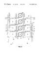
- FIG. 6is a partial plan view of a molding tool used to mold simultaneously a plurality of protective plastic epoxy resin bodies onto a plurality of surface mount grid array semiconductor packages of the type illustrated in FIG. 5;
- FIG. 7is a microscopic view of a surface plated with nodular thin dense chromium
- FIG. 8is a microscopic view of a surface plated with a conventional hard chromium plating.
- FIG. 9is a microscopic cross-sectional view of a surface plated with nodular thin dense chromium.
- FIGS. 1, 3 and 4show the sequential stages in the manufacture of a typical leadframe type of semiconductor package, while FIGS. 2, 3 and 5 show similar stages in the manufacture of a typical grid array package.
- FIG. 1a top plan view of a leadframe 10 is shown.
- the metal lead-frame 10comprises a rectangular frame 12 having a central region and a matrix of leads 14 extending from it inwardly toward the central region.
- a die mounting pad 16is supported in the central region of the frame by two or more tie-bars 18 .
- a semiconductor die 20is mounted by an adhesive to the upper surface of the die mounting pad 16 and is electrically connected to selected ones of the inner portions of the leads 14 by a plurality of fine, conductive bonding wires 22 that are bonded at their opposite ends to pads 24 on the die and selected ones of the leads 14 , respectively.
- FIG. 2A top plan view of a substrate 30 used in the manufacture of a typical grid array package is shown in FIG. 2 .
- the substrate 30comprises a rectangular sheet of insulative base material, e.g., a polyimide tape or a matrix of epoxy and fiberglass, having a plurality of conductive traces 32 formed on its upper surface and fanning out from a central region thereof.
- a semiconductor die 20is mounted by an adhesive to the upper surface of the central region of the substrate and is electrically connected to selected ones of the inner portions of the traces 32 by, e.g., a plurality of conductive bonding wires 22 that are bonded at their opposite ends to pads 24 on the die 20 and selected ones of the traces 32 , respectively.
- the traces 32connect through the substrate 30 to lands (not illustrated) on the lower surface thereof by plated-through via holes.
- the substrate 30may include a plated-on structure 34 (shown cross-hatched in FIGS. 2 and 6) of, e.g., palladium, that functions as a mold gate runner in the manner described below.
- the die 20After the die 20 is attached to the leadframe 10 (FIG. 1) or the substrate 30 (FIG. 2) and electrically connected to the leads 14 or traces 32 thereon, respectively, it is necessary to protect the relatively fragile components of the respective assemblies, viz., the die 20 , the bonding wires 22 , and the metal leads 14 or traces 32 , from harmful environmental agents, such as shock, vibration, and particularly, moisture.
- Thisis achieved by encapsulating the foregoing structures within a strong, monolithic body 40 of a high-density plastic, e.g., an epoxy resin.
- the molding of the package body 40is illustrated schematically in FIG. 3 .
- the assembly of the leadframe 10 or substrate 30 , with the die 20 attached and interconnected to it,is placed in the cavity 42 of a molding tool 44 .
- the molding tooltypically comprises an upper plate 46 and a lower plate 48 , each having a surface in mating opposition with that of the other, and into which the cavity 42 is formed.
- the cavity 42is connected to a heated reservoir, or “pot” 50 by a conduit, or “runner,” 52 , which enters into the cavity 42 through a “gate” 53 .
- the cavity 42has internal surfaces that contact the molding compound 54 during the molding process and serve to shape and form the exterior outline of the package body 40 .
- an epoxy molding compound 54 in a solid, pelletized formis dispensed into the heated pot 50 , where it is quickly melted to a molten state.
- a close-fitting piston or “ram” 56is then brought down forcefully into the pot 50 in the direction of the large arrow shown in FIG. 3, and the molten plastic compound 54 is thereby forced out of the pot, through the runner 52 and the gate 53 , and into the cavity 42 of the mold 44 to form the body 42 over the die 20 , the interconnects 22 , and the leads 14 or traces 32 of the respective assemblies.
- Air vents 55 extending through the walls of the mold 44permit the air in the cavity 42 to be expelled by the inrushing molding compound 54 .
- the upper and lower plates 46 and 48 of the moldare separated from each other, and one or more ejector pins 58 in the mold 44 are actuated in the direction of the small arrows shown in FIG. 3 to eject the newly molded leadframe package 60 or grid array package 62 , shown in cross-sectional elevation views in FIGS. 4 and 5, respectively, from the cavity 42 of the mold.
- the plastic body 40is formed entirely on the upper surface of the substrate 30 , so that the substrate forms the lower surface of the package body.
- the upper surface of the substratealso serves to define the lower surface of the runner 52 and gate 53 leading into the cavity 42 , which is conventionally let into a corner of the rectangular cavity so that the molten resin 54 flows across the cavity toward the diagonally opposite corner and the vent 55 located thereat.
- the resin 54would adhere to this portion of the upper surface of the substrate 30 to leave an undesirable plastic sprue at the location of the runner 52 after molding.
- a grid array package 62it is conventional to plate the upper surface of the substrate 30 in the region of the runner 52 and gate 53 with a noble metal, e.g., palladium, to form a mold runner gate 34 (see FIG. 2) that has a low adhesion with the molding compound, and thus permits the plastic sprue formed in the runner during molding to be easily removed from the package after molding.
- a noble metale.g., palladium
- FIG. 6is a partial top plan view of a production transfer molding apparatus 64 used to mold plastic package bodies 40 onto a plurality of grid array packages 62 simultaneously. It may be noted that, in such mass production molding, a plurality of substrates 30 are joined together end-to-end to form a strip 30 ′ for simultaneous processing of a plurality of packages.
- the plurality of generally rectangular mold cavities 42 in the lower surface of the upper plate 46 of the mold 44 , each overlying an individual substrate 30are indicated by dashed lines.
- FIG. 6illustrates the simultaneous molding of plastic bodies 40 onto a plurality of grid array packages 62
- a substantially similar apparatus and processare used to mold plastic bodies onto a plurality leadframe packages 60 of the type illustrated in FIG. 4 .
- the formulation of molding compounds 54 for semiconductor packagesis a series of compromises calculated to produce desired properties, e.g., good adhesion between the compound and the components of the package 60 or 62 , while minimizing undesirable effects, such as mold sticking and interfacial defects caused by unbalanced and/or incomplete polymer cross-linking. Accordingly, two seemingly antithetical components commonly used in the formulation of molding compounds are mold release agents and adhesion promoters.
- epoxiesare inherently excellent adhesives and will bond easily with most materials, including the surfaces of the “chase” of the molding apparatus that come into contact with the molding compound 54 during the molding process, including the pot 50 , piston 56 , runner 52 , gate 53 , cavity 42 , vent 55 , and ejector pins 58 .
- This adhesionis undesirable, because it prevents the package from being completely released from the mold 44 , and results in unacceptably cracked or cratered packages. The adhesion increases as the bonding surface becomes more porous.
- molds 44 for semiconductor packages 60 or 62are frequently made of very dense, high-hardness chrome steels, and the interior surfaces of their chases are polished very smoothly and then chrome plated to reduce the amount of adhesion between the mold 44 and the plastic body 40 of the package.
- the addition of a “release agent” to the molding compound chemistryis required to further reduce the chemical bonding between the molding compound 54 and the surfaces of the molding apparatus that come into contact with the molding compound during molding, particularly the surfaces of the cavity 42 .
- the cavity 42is, of course, necessary to form and shape the package body 40 , and also to enable complete densification of the body by the application of hydrostatic pressure to the molding compound 54 by the transfer ram or piston 56 during the molding process.
- the addition of this agent to the molding compoundis therefore especially critical in epoxy chemistry due to the large number of reactive sites present in the mold chase during the molding process.
- Mold release agents commonly usedinclude heavy waxes, such as carnauba wax. This is a natural wax extracted from palm trees. Increasingly, this compound is being replaced by synthetic ester waxes and other high-molecular-weight, non-reactive organic compounds. In some cases, two release agents are used, one for release at a low temperature, and the other for release at a high temperature, viz., the molding temperature.
- the release agentis activated thermally, and upon melting, coats the surface of all of the components in the molding matrix. This non-reactive coating inhibits interfacial bonding of the molding compound 54 and all other components within the package materials matrix, such as the leads 14 of a lead-frame 10 , the substrate 30 , the die 20 , and the bonding wires 22 . Reducing the total amount of mold release agent(s) in the molding compound would thus substantially improve the interfacial bonding within the package component matrix.
- the formation of good bonds between the reacting components of a molding compound 54 and the surface molecules of the components of the semiconductor package 60 or 62is directly proportional to surface wetting.
- the package components in contact with the molding compoundcomprise the leadframe 10 or insulative substrate 30 , including the leads 14 or conductive traces 32 , the die 20 , the connector wires 22 , the die attach adhesive, and a filler, such as silica. Poor wetting of the surfaces of these elements of the package leads to the formation of interfacial defects that act as potential sites for future propagation of cracks and subsequent penetration of the package by moisture.
- an “adhesion promoter,” or “coupling agent,”is added to the molding compound during its formulation. Due to the reduction in interfacial bonding caused by the addition of the mold release agents, it is necessary to add a higher percentage of the adhesion promoters than might otherwise thought to be desirable. This is because, in relatively larger amounts, these coupling agents can increase melt viscosity, which reduces the surface wetting of the molding compound 54 to the surface of the leadframe 10 or substrate 30 and other components in the package matrix. This increased melt viscosity is due to the premature cross-linking of the base resin and the hardener caused by the overabundance of the coupling agent during the mixing that occurs in the transfer, or injection, of the molding compound 54 into the mold cavity 42 .
- These coupling agentsare generally a reactive silane, but various other organic compounds may used. These include glycidyl ethers, and chelates, such as benzotriazole, titanates or zircoaluminates.
- the coupling agentwill have at least two reactive groups, one to react with the functional groups of the molding compound 54 , and the other to react with the materials of the other package components. In many cases, there are additional reactive groups attached to the coupling agent to allow selective coupling to specific package components, such as the lead frame 10 or the filler.
- the surfacemay be, e.g., a silica filler, or the material of the leadframe 10 , e.g., copper or aluminum. In the case of the leadframe material, the primary bonding mechanism is, in most applications, from the coupling agent to a thin oxide surface present thereon.
- EOCNepoxidized ortho cresol novolac
- newer epoxy formulations of even higher functionality than the EOCNDue to this higher functionality, the cross-link density of these compounds is higher. As the cross-link density increases, the more closely packed will be the final polymer. This results in compounds that are more impervious to moisture penetration, have higher glass transition temperatures and other enhanced properties.
- the newer epoxy compoundsare Biphenyl, Dicyclopentadene, and so-called “Multifunctional” compounds. And, as in the case of EOCN, the reduction of mold release agents and adhesion promoters in these latter, enhanced epoxies is highly desirable.
- the reduction or elimination of the waxy mold release agentswill present a more active surface for chemical bonding.
- this goalcannot be achieved unless the surfaces of the chase of the molding apparatus that come into contact with the molding compound 54 during the molding process, including the pot 50 , piston 56 , runner 52 , gate 53 , cavity 42 , vent 55 , and ejector pins 58 , are made of or coated with a material that is substantially non-reactive with the highly reactive epoxy molding compound.
- such a reduction or elimination of the release agentwould permit a concomitant reduction or elimination of the coupling agent, or adhesion promoter, in the molding compound, which would better balance the formulation and prevent premature cross-linking of the molding compound during the mixing and transfer to the contacting surfaces of the molding apparatus.
- the molding tool 44is made of a very dense, high-hardness steel, e.g., a chrome steel, and all of the surfaces of the chase of the mold 44 that come into contact with the molding compound 54 during the molding process, including the pot 50 , piston 56 , runner 52 , gate 53 , cavity 42 , vent 55 , and ejector pins 58 , are plated with a coating of “nodular thin dense chromium” (“NTDC”).
- NTDCnodular thin dense chromium
- this reduction in the reactivity between the mold 44 and the molding compound 54permits a corresponding reduction or elimination of both the release agents and coupling agents otherwise necessary in the molding compound, thereby providing substantially improved adhesion between the molding compound and the components of the package matrix and preventing premature cross-linking of the molding compound during its mixing and transfer to the contacting chase surfaces of the mold 44 .
- the hard nodular chromium coatingcan be applied to the affected surfaces of the mold 44 by the commercially available Armoloy® process that is widely available from franchised Armoloy dealers located throughout the U.S. and Europe.
- Armoloy dealerslocated throughout the U.S. and Europe.
- a listing of Armoloy dealerscan be obtained from the Armoloy Company of Philadelphia, 1105 Miller Avenue, Croydon, Pa. 19021.
- the ARMOLOY processis a proprietary chromium electroplating process that produces a nodular thin dense chromium (“NTDC”) coating having a hardness in excess of 70 R C (1,020-1100 Vickers Diamond hardness) and an extremely low coefficient of friction, e.g., a static coefficient of friction of 0.14.
- the finishis applied in an extremely thin (about 0.0001′′ to about 0.0002′′ thick) coating, and retains its desirable properties at elevated temperatures, viz., 1400° F. As plated, it has a gray, satin-matte finish of about 8 RMS.
- FIG. 7is a microscopic view of a surface plated with nodular thin dense chromium coating 70 .
- the extremely small, nodular characteristic of this surfacemay be compared to the much larger nodular characteristics of a surface plated with a conventional hard chromium plating 72 shown in the microscopic view of FIG. 8 .
- FIG. 9is a microscopic cross-sectional view showing the extreme thinness and very fine nodular nature of the NTDC coating 70 , as compared to the relatively coarser nodular structure of an underlying high-hardness, chrome steel molding tool 44 upon which the NTDC coating has been plated.
- the proprietary platingis not recommended for use on aluminum, magnesium, or titanium, it is compatible with all ferrous metals, and in particular, the type of dense, high-hardness chrome steels used to make the semiconductor package molding tool 44 .
- Surfaces plated with the finishexhibit extremely low adhesion with epoxy resin.
- the mold 44will exhibit a superior non-reactivity with the molding compound 54 of the package body 40 , and hence, exceptionally good package release.
- NTDC electroplated coatingscan be applied from a solution containing chromic acid (CrO 3 ) and a catalytic anion, as described in, for example, “Hard Chromium Plating,” Hyman Chessin and Everett H. Fernald, Jr., Metals Handbook, Ninth Ed. , Vol. 5, “Surface Cleaning, Finishing, and Coating,” (1982) pp. 170-187.
- NTDC coatings of exceptionally high hardnessmay be obtained by using high current densities in plating baths employing a mixed catalyst.
- Other processes that are believed to provide NTDC platingsare described in U.S. Pat. Nos. 4,092,226 to N. Laing et al., and 4,717,456 to H. Chessin et al.
Landscapes
- Engineering & Computer Science (AREA)
- Manufacturing & Machinery (AREA)
- Mechanical Engineering (AREA)
- Computer Hardware Design (AREA)
- Microelectronics & Electronic Packaging (AREA)
- Power Engineering (AREA)
- Physics & Mathematics (AREA)
- Condensed Matter Physics & Semiconductors (AREA)
- General Physics & Mathematics (AREA)
- Encapsulation Of And Coatings For Semiconductor Or Solid State Devices (AREA)
- Moulds For Moulding Plastics Or The Like (AREA)
Abstract
Description
Claims (13)
Priority Applications (1)
| Application Number | Priority Date | Filing Date | Title |
|---|---|---|---|
| US09/441,115US6309916B1 (en) | 1999-11-17 | 1999-11-17 | Method of molding plastic semiconductor packages |
Applications Claiming Priority (1)
| Application Number | Priority Date | Filing Date | Title |
|---|---|---|---|
| US09/441,115US6309916B1 (en) | 1999-11-17 | 1999-11-17 | Method of molding plastic semiconductor packages |
Publications (1)
| Publication Number | Publication Date |
|---|---|
| US6309916B1true US6309916B1 (en) | 2001-10-30 |
Family
ID=23751577
Family Applications (1)
| Application Number | Title | Priority Date | Filing Date |
|---|---|---|---|
| US09/441,115Expired - LifetimeUS6309916B1 (en) | 1999-11-17 | 1999-11-17 | Method of molding plastic semiconductor packages |
Country Status (1)
| Country | Link |
|---|---|
| US (1) | US6309916B1 (en) |
Cited By (39)
| Publication number | Priority date | Publication date | Assignee | Title |
|---|---|---|---|---|
| US20020025353A1 (en)* | 2000-08-31 | 2002-02-28 | Williams Vernon M. | Transfer molding and underfilling method and apparatus |
| US6358773B1 (en)* | 2000-12-27 | 2002-03-19 | Vincent Lin | Method of making substrate for use in forming image sensor package |
| US6444500B1 (en)* | 1999-12-24 | 2002-09-03 | Fujitsu Limited | Split-mold and method for manufacturing semiconductor device by using the same |
| US20020151103A1 (en)* | 2001-04-06 | 2002-10-17 | Shigeru Nakamura | Semiconductor device and method of manufacturing the same |
| US20020180024A1 (en)* | 2001-05-29 | 2002-12-05 | Siliconware Precision Industries Co., Ltd., Taiwan R.O.C. | Semiconductor package and method for fabricating the same |
| US20030062642A1 (en)* | 2001-10-02 | 2003-04-03 | Williams Vernon M. | Leadframe and method for removing cleaning compound flash from mold vents |
| US20030067061A1 (en)* | 2001-10-10 | 2003-04-10 | Williams Vernon M. | Leadframe and method for reducing mold compound adhesion problems |
| US6566164B1 (en)* | 2000-12-07 | 2003-05-20 | Amkor Technology, Inc. | Exposed copper strap in a semiconductor package |
| US6580620B1 (en)* | 1999-04-14 | 2003-06-17 | Amkor Technology, Inc. | Matrix type printed circuit board for semiconductor packages |
| US6653173B2 (en)* | 2000-06-16 | 2003-11-25 | Micron Technology, Inc. | Method and apparatus for packaging a microelectronic die |
| US20030218263A1 (en)* | 2002-03-25 | 2003-11-27 | Stephan Blaszczak | Electronic component with a semiconductor chip, method of producing an electronic component and a panel with a plurality of electronic components |
| US20040031461A1 (en)* | 2002-08-19 | 2004-02-19 | Trw Inc. | Chrome plated engine valve |
| US6700077B2 (en)* | 2001-06-07 | 2004-03-02 | Advanced Semiconductor Engineering, Inc. | Packaging substrate with electrostatic discharge protection |
| US6750082B2 (en) | 2002-09-13 | 2004-06-15 | Advanpack Solutions Pte. Ltd. | Method of assembling a package with an exposed die backside with and without a heatsink for flip-chip |
| US6796028B2 (en) | 2000-08-23 | 2004-09-28 | Micron Technology, Inc. | Method of Interconnecting substrates for electrical coupling of microelectronic components |
| US20050035435A1 (en)* | 2001-08-30 | 2005-02-17 | James Steven L. | Method for fabricating semiconductor components using mold cavities having runners configured to minimize venting |
| US20050067790A1 (en)* | 2003-09-26 | 2005-03-31 | Smith Thomas J. | Piston ring having chromium coating |
| US20050124785A1 (en)* | 2003-12-08 | 2005-06-09 | Matayabas James C.Jr. | Encapsulant mixture having a polymer bound catalyst |
| US20050136656A1 (en)* | 2003-12-19 | 2005-06-23 | Zeng Xian T. | Process for depositing composite coating on a surface |
| US6979595B1 (en) | 2000-08-24 | 2005-12-27 | Micron Technology, Inc. | Packaged microelectronic devices with pressure release elements and methods for manufacturing and using such packaged microelectronic devices |
| US20060043641A1 (en)* | 2004-08-31 | 2006-03-02 | Bunshi Kuratomi | Method of manufacturing a semiconductor device |
| US7026710B2 (en)* | 2000-01-21 | 2006-04-11 | Texas Instruments Incorporated | Molded package for micromechanical devices and method of fabrication |
| US7061082B2 (en) | 1997-02-25 | 2006-06-13 | Micron Technology, Inc. | Semiconductor die with attached heat sink and transfer mold |
| US7101737B2 (en) | 2000-08-28 | 2006-09-05 | Micron Technology, Inc. | Method of encapsulating interconnecting units in packaged microelectronic devices |
| US20060226477A1 (en)* | 2005-03-29 | 2006-10-12 | Brar Berinder P S | Substrate driven field-effect transistor |
| US7220615B2 (en) | 2001-06-11 | 2007-05-22 | Micron Technology, Inc. | Alternative method used to package multimedia card by transfer molding |
| WO2006101577A3 (en)* | 2005-03-16 | 2007-06-21 | Freescale Semiconductor Inc | Lead frame panel and a plurality of half-etched connection bars |
| US20080029873A1 (en)* | 2006-08-03 | 2008-02-07 | Dal Jae Lee | Integrated circuit package system with molding vents |
| US20080036050A1 (en)* | 2006-08-08 | 2008-02-14 | Lin Paul T | Package with solder-filled via holes in molding layers |
| US20080160658A1 (en)* | 2007-01-03 | 2008-07-03 | Harvatek Corporation | Mold structure for packaging led chips and method thereof |
| US20080251739A1 (en)* | 2007-04-13 | 2008-10-16 | Yoon Hwa Choi | Optical coupler package |
| US20100081218A1 (en)* | 2008-09-26 | 2010-04-01 | Craig Hardin | Forming Light Emitting Devices Including Custom Wavelength Conversion Structures |
| US7833456B2 (en) | 2007-02-23 | 2010-11-16 | Micron Technology, Inc. | Systems and methods for compressing an encapsulant adjacent a semiconductor workpiece |
| US20110169195A1 (en)* | 2010-01-11 | 2011-07-14 | Cheol-Joon Yoo | Molding apparatus and molding method |
| US20110198741A1 (en)* | 2010-02-17 | 2011-08-18 | Analog Devices, Inc. | Integrated Circuit Package with Enlarged Die Paddle |
| EP2709143A1 (en)* | 2012-09-18 | 2014-03-19 | Gemalto SA | Moulding method for manufacturing an electronic package |
| CN104015317A (en)* | 2014-07-04 | 2014-09-03 | 苏州新协力特种工业模板有限公司 | Sliding thimble mechanism of injection mold system |
| WO2015140213A1 (en)* | 2014-03-21 | 2015-09-24 | Osram Opto Semiconductors Gmbh | Method for producing a housing for an electronic component and an electronic component, housing for an electronic component, and electronic component |
| US10943800B2 (en) | 2017-04-18 | 2021-03-09 | Advanced Semiconductor Engineering, Inc. | Semiconductor package device and method of forming package body |
Citations (8)
| Publication number | Priority date | Publication date | Assignee | Title |
|---|---|---|---|---|
| US4092226A (en) | 1974-12-11 | 1978-05-30 | Nikolaus Laing | Process for the treatment of metal surfaces by electro-deposition of metal coatings at high current densities |
| US4615857A (en)* | 1984-11-30 | 1986-10-07 | Motorola, Inc. | Encapsulation means and method for reducing flash |
| US4717456A (en) | 1986-01-06 | 1988-01-05 | M&T Chemicals | Two-step electrolytic activation process for chromium electrodeposition |
| US4872825A (en)* | 1984-05-23 | 1989-10-10 | Ross Milton I | Method and apparatus for making encapsulated electronic circuit devices |
| JPH09199522A (en) | 1996-01-23 | 1997-07-31 | Seiko Epson Corp | Method for manufacturing semiconductor device |
| US5766649A (en)* | 1995-12-15 | 1998-06-16 | Nec Corporation | Resin sealing mold die set with less resin remainder for semiconductor device |
| JPH10286845A (en) | 1997-04-15 | 1998-10-27 | Seiko Epson Corp | Resin sealing mold and method of manufacturing resin sealed semiconductor device |
| US5829240A (en)* | 1997-03-17 | 1998-11-03 | A. B. Carter, Inc. | Spinning ring having improved traveler bearing surface |
- 1999
- 1999-11-17USUS09/441,115patent/US6309916B1/ennot_activeExpired - Lifetime
Patent Citations (8)
| Publication number | Priority date | Publication date | Assignee | Title |
|---|---|---|---|---|
| US4092226A (en) | 1974-12-11 | 1978-05-30 | Nikolaus Laing | Process for the treatment of metal surfaces by electro-deposition of metal coatings at high current densities |
| US4872825A (en)* | 1984-05-23 | 1989-10-10 | Ross Milton I | Method and apparatus for making encapsulated electronic circuit devices |
| US4615857A (en)* | 1984-11-30 | 1986-10-07 | Motorola, Inc. | Encapsulation means and method for reducing flash |
| US4717456A (en) | 1986-01-06 | 1988-01-05 | M&T Chemicals | Two-step electrolytic activation process for chromium electrodeposition |
| US5766649A (en)* | 1995-12-15 | 1998-06-16 | Nec Corporation | Resin sealing mold die set with less resin remainder for semiconductor device |
| JPH09199522A (en) | 1996-01-23 | 1997-07-31 | Seiko Epson Corp | Method for manufacturing semiconductor device |
| US5829240A (en)* | 1997-03-17 | 1998-11-03 | A. B. Carter, Inc. | Spinning ring having improved traveler bearing surface |
| JPH10286845A (en) | 1997-04-15 | 1998-10-27 | Seiko Epson Corp | Resin sealing mold and method of manufacturing resin sealed semiconductor device |
Non-Patent Citations (9)
| Title |
|---|
| "Armoloy(R) Nodular Thin Dense Chromium"and "Special Armoloy(C) Properties", pp. 1-2, Website http:/www.armoloycompany.com/properties.html. |
| "Armoloy(R) Nodular Thin Dense Chromium"-Typical Industries, pp. 1-2, Website http://www.armoloycompany.com/applications.html. |
| "Armoloy® Nodular Thin Dense Chromium"and "Special Armoloy© Properties", pp. 1-2, Website http:/www.armoloycompany.com/properties.html. |
| "Armoloy® Nodular Thin Dense Chromium"—Typical Industries, pp. 1-2, Website http://www.armoloycompany.com/applications.html. |
| Armoloy Chromium Plating by Armoloy Company of Philadelphia, pp. 1-2, Website, http://www.armoloycompany.com/. |
| Armoloy Company of Philadelphia-Comparison Chart, Characteristics, Performance, pp. 1, Website, http://www.armoloycompany.com/compare.html. |
| Armoloy Company of Philadelphia-Working with Armoloy(R) of Philadelphia is as easy as . . . 1-2-3, pp. 1-2, Website, http://www.armoloycompany.com/process.html. |
| Armoloy Company of Philadelphia—Working with Armoloy® of Philadelphia is as easy as . . . 1-2-3, pp. 1-2, Website, http://www.armoloycompany.com/process.html. |
| Chessin et al., "Hard Chromium Plating," Metals Handbook, Ninth Ed., vol. 5, pp. 170-187. |
Cited By (74)
| Publication number | Priority date | Publication date | Assignee | Title |
|---|---|---|---|---|
| US7061082B2 (en) | 1997-02-25 | 2006-06-13 | Micron Technology, Inc. | Semiconductor die with attached heat sink and transfer mold |
| US6580620B1 (en)* | 1999-04-14 | 2003-06-17 | Amkor Technology, Inc. | Matrix type printed circuit board for semiconductor packages |
| US6563207B2 (en) | 1999-12-24 | 2003-05-13 | Fujitsu Limited | Split-mold and method for manufacturing semiconductor device by using the same |
| US6444500B1 (en)* | 1999-12-24 | 2002-09-03 | Fujitsu Limited | Split-mold and method for manufacturing semiconductor device by using the same |
| US7026710B2 (en)* | 2000-01-21 | 2006-04-11 | Texas Instruments Incorporated | Molded package for micromechanical devices and method of fabrication |
| US6677675B2 (en) | 2000-06-16 | 2004-01-13 | Micron Technology, Inc. | Microelectronic devices and microelectronic die packages |
| US6683388B2 (en) | 2000-06-16 | 2004-01-27 | Micron Technology, Inc. | Method and apparatus for packaging a microelectronic die |
| US6653173B2 (en)* | 2000-06-16 | 2003-11-25 | Micron Technology, Inc. | Method and apparatus for packaging a microelectronic die |
| US6664139B2 (en)* | 2000-06-16 | 2003-12-16 | Micron Technology, Inc. | Method and apparatus for packaging a microelectronic die |
| US6796028B2 (en) | 2000-08-23 | 2004-09-28 | Micron Technology, Inc. | Method of Interconnecting substrates for electrical coupling of microelectronic components |
| US6983551B2 (en) | 2000-08-23 | 2006-01-10 | Micron Technology, Inc. | Interconnecting substrates for electrical coupling of microelectronic components |
| US6982386B2 (en) | 2000-08-23 | 2006-01-03 | Micron Technology, Inc. | Interconnecting substrates for electrical coupling of microelectronic components |
| US7049685B2 (en) | 2000-08-24 | 2006-05-23 | Micron Technology, Inc. | Packaged microelectronic devices with pressure release elements and methods for manufacturing and using such packaged microelectronic devices |
| US6979595B1 (en) | 2000-08-24 | 2005-12-27 | Micron Technology, Inc. | Packaged microelectronic devices with pressure release elements and methods for manufacturing and using such packaged microelectronic devices |
| US7101737B2 (en) | 2000-08-28 | 2006-09-05 | Micron Technology, Inc. | Method of encapsulating interconnecting units in packaged microelectronic devices |
| US7332376B2 (en) | 2000-08-28 | 2008-02-19 | Micron Technology, Inc. | Method of encapsulating packaged microelectronic devices with a barrier |
| US20020115237A1 (en)* | 2000-08-31 | 2002-08-22 | Williams Vernon M. | Transfer molding and underfilling method and apparatus |
| US20020025353A1 (en)* | 2000-08-31 | 2002-02-28 | Williams Vernon M. | Transfer molding and underfilling method and apparatus |
| US6830954B2 (en)* | 2000-08-31 | 2004-12-14 | Micron Technology, Inc. | Transfer molding and underfilling method and apparatus |
| US6838319B1 (en) | 2000-08-31 | 2005-01-04 | Micron Technology, Inc. | Transfer molding and underfilling method and apparatus including orienting the active surface of a semiconductor substrate substantially vertically |
| US6863516B2 (en) | 2000-08-31 | 2005-03-08 | Micron Technology, Inc. | Transfer molding and underfilling apparatus |
| US6723582B2 (en) | 2000-12-07 | 2004-04-20 | Amkor Technology, Inc. | Method of making a semiconductor package having exposed metal strap |
| US6566164B1 (en)* | 2000-12-07 | 2003-05-20 | Amkor Technology, Inc. | Exposed copper strap in a semiconductor package |
| US6358773B1 (en)* | 2000-12-27 | 2002-03-19 | Vincent Lin | Method of making substrate for use in forming image sensor package |
| US6951774B2 (en)* | 2001-04-06 | 2005-10-04 | Renesas Technology Corp. | Semiconductor device and method of manufacturing the same |
| US20020151103A1 (en)* | 2001-04-06 | 2002-10-17 | Shigeru Nakamura | Semiconductor device and method of manufacturing the same |
| US20020180024A1 (en)* | 2001-05-29 | 2002-12-05 | Siliconware Precision Industries Co., Ltd., Taiwan R.O.C. | Semiconductor package and method for fabricating the same |
| US6867487B2 (en)* | 2001-05-29 | 2005-03-15 | Siliconware Precision Industries Co., Ltd. | Flash-preventing semiconductor package |
| US6700077B2 (en)* | 2001-06-07 | 2004-03-02 | Advanced Semiconductor Engineering, Inc. | Packaging substrate with electrostatic discharge protection |
| US7220615B2 (en) | 2001-06-11 | 2007-05-22 | Micron Technology, Inc. | Alternative method used to package multimedia card by transfer molding |
| US20050040506A1 (en)* | 2001-08-30 | 2005-02-24 | James Steven L. | Semiconductor component having dummy segments with trapped corner air |
| US7265453B2 (en)* | 2001-08-30 | 2007-09-04 | Micron Technology, Inc. | Semiconductor component having dummy segments with trapped corner air |
| US7186589B2 (en) | 2001-08-30 | 2007-03-06 | Micron Technology, Inc. | Method for fabricating semiconductor components using mold cavities having runners configured to minimize venting |
| US20050035435A1 (en)* | 2001-08-30 | 2005-02-17 | James Steven L. | Method for fabricating semiconductor components using mold cavities having runners configured to minimize venting |
| US7029256B2 (en)* | 2001-10-02 | 2006-04-18 | Micron Technology, Inc. | Leadframe and method for removing cleaning compound flash from mold vents |
| US20030062642A1 (en)* | 2001-10-02 | 2003-04-03 | Williams Vernon M. | Leadframe and method for removing cleaning compound flash from mold vents |
| US7264456B2 (en) | 2001-10-10 | 2007-09-04 | Micron Technology, Inc. | Leadframe and method for reducing mold compound adhesion problems |
| US20060082021A1 (en)* | 2001-10-10 | 2006-04-20 | Williams Vernon M | Leadframe and method for reducing mold compound adhesion problems |
| US20030067061A1 (en)* | 2001-10-10 | 2003-04-10 | Williams Vernon M. | Leadframe and method for reducing mold compound adhesion problems |
| US20050067721A1 (en)* | 2002-03-25 | 2005-03-31 | Infineon Technologies Ag | Method of producing an electronic component and a panel with a plurality of electronic components |
| US6873060B2 (en)* | 2002-03-25 | 2005-03-29 | Infineon Technologies Ag | Electronic component with a semiconductor chip, method of producing an electronic component and a panel with a plurality of electronic components |
| US7223639B2 (en) | 2002-03-25 | 2007-05-29 | Infineon Technologies Ag | Method of producing an electronic component and a panel with a plurality of electronic components |
| US20030218263A1 (en)* | 2002-03-25 | 2003-11-27 | Stephan Blaszczak | Electronic component with a semiconductor chip, method of producing an electronic component and a panel with a plurality of electronic components |
| US7011067B2 (en) | 2002-08-19 | 2006-03-14 | Trw | Chrome plated engine valve |
| US20040031461A1 (en)* | 2002-08-19 | 2004-02-19 | Trw Inc. | Chrome plated engine valve |
| US6750082B2 (en) | 2002-09-13 | 2004-06-15 | Advanpack Solutions Pte. Ltd. | Method of assembling a package with an exposed die backside with and without a heatsink for flip-chip |
| US20050067790A1 (en)* | 2003-09-26 | 2005-03-31 | Smith Thomas J. | Piston ring having chromium coating |
| US20050124785A1 (en)* | 2003-12-08 | 2005-06-09 | Matayabas James C.Jr. | Encapsulant mixture having a polymer bound catalyst |
| US6974728B2 (en)* | 2003-12-08 | 2005-12-13 | Intel Corporation | Encapsulant mixture having a polymer bound catalyst |
| US20050136656A1 (en)* | 2003-12-19 | 2005-06-23 | Zeng Xian T. | Process for depositing composite coating on a surface |
| US20060043641A1 (en)* | 2004-08-31 | 2006-03-02 | Bunshi Kuratomi | Method of manufacturing a semiconductor device |
| US8119050B2 (en)* | 2004-08-31 | 2012-02-21 | Renesas Electronics Corporation | Method of manufacturing a semiconductor device |
| WO2006101577A3 (en)* | 2005-03-16 | 2007-06-21 | Freescale Semiconductor Inc | Lead frame panel and a plurality of half-etched connection bars |
| US20060226477A1 (en)* | 2005-03-29 | 2006-10-12 | Brar Berinder P S | Substrate driven field-effect transistor |
| US7863761B2 (en) | 2006-08-03 | 2011-01-04 | Stats Chippac Ltd. | Integrated circuit package system with molding vents |
| US20080029873A1 (en)* | 2006-08-03 | 2008-02-07 | Dal Jae Lee | Integrated circuit package system with molding vents |
| US7667338B2 (en)* | 2006-08-08 | 2010-02-23 | Lin Paul T | Package with solder-filled via holes in molding layers |
| US20080036050A1 (en)* | 2006-08-08 | 2008-02-14 | Lin Paul T | Package with solder-filled via holes in molding layers |
| US20080160658A1 (en)* | 2007-01-03 | 2008-07-03 | Harvatek Corporation | Mold structure for packaging led chips and method thereof |
| US7803641B2 (en)* | 2007-01-03 | 2010-09-28 | Harvatek Corporation | Mold structure for packaging LED chips and method thereof |
| US7833456B2 (en) | 2007-02-23 | 2010-11-16 | Micron Technology, Inc. | Systems and methods for compressing an encapsulant adjacent a semiconductor workpiece |
| US20080251739A1 (en)* | 2007-04-13 | 2008-10-16 | Yoon Hwa Choi | Optical coupler package |
| US7659531B2 (en)* | 2007-04-13 | 2010-02-09 | Fairchild Semiconductor Corporation | Optical coupler package |
| CN101657748B (en)* | 2007-04-13 | 2013-01-16 | 费查尔德半导体有限公司 | Optical coupler package |
| US20100081218A1 (en)* | 2008-09-26 | 2010-04-01 | Craig Hardin | Forming Light Emitting Devices Including Custom Wavelength Conversion Structures |
| US20110169195A1 (en)* | 2010-01-11 | 2011-07-14 | Cheol-Joon Yoo | Molding apparatus and molding method |
| US20110198741A1 (en)* | 2010-02-17 | 2011-08-18 | Analog Devices, Inc. | Integrated Circuit Package with Enlarged Die Paddle |
| US8193620B2 (en)* | 2010-02-17 | 2012-06-05 | Analog Devices, Inc. | Integrated circuit package with enlarged die paddle |
| EP2709143A1 (en)* | 2012-09-18 | 2014-03-19 | Gemalto SA | Moulding method for manufacturing an electronic package |
| WO2014044684A1 (en)* | 2012-09-18 | 2014-03-27 | Gemalto Sa | Moulding method for producing an electronic housing |
| WO2015140213A1 (en)* | 2014-03-21 | 2015-09-24 | Osram Opto Semiconductors Gmbh | Method for producing a housing for an electronic component and an electronic component, housing for an electronic component, and electronic component |
| US10040230B2 (en) | 2014-03-21 | 2018-08-07 | Osram Opto Semiconductors Gmbh | Method of producing a housing for an electronic device and an electronic device, housing for an electronic device, and electronic device |
| CN104015317A (en)* | 2014-07-04 | 2014-09-03 | 苏州新协力特种工业模板有限公司 | Sliding thimble mechanism of injection mold system |
| US10943800B2 (en) | 2017-04-18 | 2021-03-09 | Advanced Semiconductor Engineering, Inc. | Semiconductor package device and method of forming package body |
Similar Documents
| Publication | Publication Date | Title |
|---|---|---|
| US6309916B1 (en) | Method of molding plastic semiconductor packages | |
| US7262514B2 (en) | Epoxy resin composition for semiconductor encapsulation, semiconductor device using the same, and process for producing semiconductor device | |
| EP0977251B1 (en) | Resin sealed semiconductor device and method for manufacturing the same | |
| US6108210A (en) | Flip chip devices with flexible conductive adhesive | |
| US6498055B2 (en) | Semiconductor device, method of manufacturing semiconductor device, resin molding die, and semiconductor manufacturing system | |
| US6872597B2 (en) | Method of manufacturing a semiconductor device and a semiconductor device | |
| US6214446B1 (en) | Resin film and a method for connecting electronic parts by the use thereof | |
| US5474958A (en) | Method for making semiconductor device having no die supporting surface | |
| US7781897B2 (en) | Semiconductor device and method for producing the same | |
| JP2001513946A (en) | Vertical interconnect electronic assemblies and compositions useful therein | |
| JP3652488B2 (en) | Manufacturing method of resin package | |
| JPH1027825A (en) | Semiconductor element mounting substrate, method of manufacturing semiconductor element mounting substrate, semiconductor device, and method of manufacturing semiconductor device | |
| US20040142511A1 (en) | Lead frame and production process thereof and production process of thermally conductive substrate | |
| KR100518643B1 (en) | Semiconductor device, method of fabricating the same, and printing mask | |
| TW202249220A (en) | Configurable leaded package | |
| US11862600B2 (en) | Method of forming a chip package and chip package | |
| EP1090535A1 (en) | Flip chip devices with flexible conductive adhesive | |
| JP4381630B2 (en) | Resin-sealed module device for automobile control | |
| KR960010011B1 (en) | Process for manufacturing plastic pin grid arrays and the product produced thereby | |
| JPH10261741A (en) | Semiconductor device and manufacture of semiconductor device | |
| US20200185322A1 (en) | Semiconductor device connections with sintered nanoparticles | |
| JP3572764B2 (en) | Bare chip sealing method and bare chip sealing substrate | |
| JPH0434958A (en) | Resin sealing type semiconductor device and manufacture thereof | |
| WO1998034277A1 (en) | Improved leadframe structure with preplated leads and process for manufacturing the same | |
| JPS61253845A (en) | Lead frame |
Legal Events
| Date | Code | Title | Description |
|---|---|---|---|
| AS | Assignment | Owner name:AMKOR TECHNOLOGY, INC., ARIZONA Free format text:ASSIGNMENT OF ASSIGNORS INTEREST;ASSIGNORS:CROWLEY, SEAN T.;CHENEY, GERALD L.;RUZU, DAVID S.;REEL/FRAME:010407/0037 Effective date:19991112 | |
| AS | Assignment | Owner name:AMKOR TECHNOLOGY, INC., ARIZONA Free format text:ASSIGNMENT OF ASSIGNORS INTEREST;ASSIGNORS:CHENEY, GERALD L.;CROWLEY, SEAN T.;RAZU, DAVID S.;REEL/FRAME:011099/0089 Effective date:20000523 | |
| AS | Assignment | Owner name:SOCIETE GENERALE, NEW YORK Free format text:SECURITY INTEREST;ASSIGNORS:AMKOR TECHNOLOGY, INC.;GUARDIAN ASSETS, INC.;REEL/FRAME:011491/0917 Effective date:20000428 | |
| AS | Assignment | Owner name:CITICORP USA, INC., NEW YORK Free format text:SECURITY INTEREST;ASSIGNORS:SOCIETE GENERALE;GUARDIAN ASSETS, INC.;REEL/FRAME:011682/0416 Effective date:20010330 | |
| STCF | Information on status: patent grant | Free format text:PATENTED CASE | |
| CC | Certificate of correction | ||
| AS | Assignment | Owner name:CITICORP USA, INC. AS "COLLATERAL AGENT", DELAWARE Free format text:SECURITY INTEREST;ASSIGNORS:AMKOR TECHNOLOGY, INC.;GUARDIAN ASSETS, INC.;REEL/FRAME:013974/0893 Effective date:20030422 | |
| AS | Assignment | Owner name:CITICORP NORTH AMERICA, INC. AS ADMINISTRATIVE AGE Free format text:SECURITY AGREEMENT;ASSIGNORS:AMKOR TECHNOLOGY, INC.;GUARDIAN ASSETS, INC.;REEL/FRAME:014885/0691 Effective date:20040629 | |
| AS | Assignment | Owner name:AMKOR TECHNOLOGY, INC., PENNSYLVANIA Free format text:RELEASE OF LIEN ON PATENTS;ASSIGNOR:CITICORP USA, INC. AS COLLATERAL AGENT;REEL/FRAME:015603/0572 Effective date:20040629 | |
| AS | Assignment | Owner name:CITICORP NORTH AMERICA, INC. AS "AGENT", NEW YORK Free format text:SECURITY AGREEMENT;ASSIGNORS:AMKOR TECHNOLOGY, INC.;GUARDIAN ASSETS, INC.;REEL/FRAME:015942/0521 Effective date:20041027 | |
| FEPP | Fee payment procedure | Free format text:PAYOR NUMBER ASSIGNED (ORIGINAL EVENT CODE: ASPN); ENTITY STATUS OF PATENT OWNER: LARGE ENTITY | |
| FPAY | Fee payment | Year of fee payment:4 | |
| AS | Assignment | Owner name:BANK OF AMERICA, N.A., TEXAS Free format text:SECURITY AGREEMENT;ASSIGNOR:AMKOR TECHNOLOGY, INC.;REEL/FRAME:017379/0630 Effective date:20051123 Owner name:AMKOR TECHNOLOGY, INC., ARIZONA Free format text:TERMINATION & RELEASE OF PATENT SECURITY AGREEMENT;ASSIGNOR:CITICORP NORTH AMERICA, INC.;REEL/FRAME:017388/0868 Effective date:20051128 | |
| FPAY | Fee payment | Year of fee payment:8 | |
| FPAY | Fee payment | Year of fee payment:12 | |
| AS | Assignment | Owner name:BANK OF AMERICA, N.A., AS AGENT, CALIFORNIA Free format text:SECURITY INTEREST;ASSIGNOR:AMKOR TECHNOLOGY, INC.;REEL/FRAME:046683/0139 Effective date:20180713 | |
| AS | Assignment | Owner name:AMKOR TECHNOLOGY SINGAPORE HOLDING PTE.LTD., SINGAPORE Free format text:ASSIGNMENT OF ASSIGNORS INTEREST;ASSIGNOR:AMKOR TECHNOLOGY, INC.;REEL/FRAME:054036/0599 Effective date:20191119 |