US6309915B1 - Semiconductor chip package with expander ring and method of making same - Google Patents
Semiconductor chip package with expander ring and method of making sameDownload PDFInfo
- Publication number
- US6309915B1 US6309915B1US09/245,224US24522499AUS6309915B1US 6309915 B1US6309915 B1US 6309915B1US 24522499 AUS24522499 AUS 24522499AUS 6309915 B1US6309915 B1US 6309915B1
- Authority
- US
- United States
- Prior art keywords
- semiconductor chip
- dielectric element
- expander ring
- chip
- cte
- Prior art date
- Legal status (The legal status is an assumption and is not a legal conclusion. Google has not performed a legal analysis and makes no representation as to the accuracy of the status listed.)
- Expired - Lifetime
Links
Images


Classifications
- H—ELECTRICITY
- H01—ELECTRIC ELEMENTS
- H01L—SEMICONDUCTOR DEVICES NOT COVERED BY CLASS H10
- H01L21/00—Processes or apparatus adapted for the manufacture or treatment of semiconductor or solid state devices or of parts thereof
- H01L21/02—Manufacture or treatment of semiconductor devices or of parts thereof
- H01L21/04—Manufacture or treatment of semiconductor devices or of parts thereof the devices having potential barriers, e.g. a PN junction, depletion layer or carrier concentration layer
- H01L21/50—Assembly of semiconductor devices using processes or apparatus not provided for in a single one of the groups H01L21/18 - H01L21/326 or H10D48/04 - H10D48/07 e.g. sealing of a cap to a base of a container
- H01L21/56—Encapsulations, e.g. encapsulation layers, coatings
- H01L21/568—Temporary substrate used as encapsulation process aid
- H—ELECTRICITY
- H01—ELECTRIC ELEMENTS
- H01L—SEMICONDUCTOR DEVICES NOT COVERED BY CLASS H10
- H01L21/00—Processes or apparatus adapted for the manufacture or treatment of semiconductor or solid state devices or of parts thereof
- H01L21/67—Apparatus specially adapted for handling semiconductor or electric solid state devices during manufacture or treatment thereof; Apparatus specially adapted for handling wafers during manufacture or treatment of semiconductor or electric solid state devices or components ; Apparatus not specifically provided for elsewhere
- H01L21/683—Apparatus specially adapted for handling semiconductor or electric solid state devices during manufacture or treatment thereof; Apparatus specially adapted for handling wafers during manufacture or treatment of semiconductor or electric solid state devices or components ; Apparatus not specifically provided for elsewhere for supporting or gripping
- H01L21/6835—Apparatus specially adapted for handling semiconductor or electric solid state devices during manufacture or treatment thereof; Apparatus specially adapted for handling wafers during manufacture or treatment of semiconductor or electric solid state devices or components ; Apparatus not specifically provided for elsewhere for supporting or gripping using temporarily an auxiliary support
- H—ELECTRICITY
- H01—ELECTRIC ELEMENTS
- H01L—SEMICONDUCTOR DEVICES NOT COVERED BY CLASS H10
- H01L23/00—Details of semiconductor or other solid state devices
- H01L23/16—Fillings or auxiliary members in containers or encapsulations, e.g. centering rings
- H—ELECTRICITY
- H01—ELECTRIC ELEMENTS
- H01L—SEMICONDUCTOR DEVICES NOT COVERED BY CLASS H10
- H01L23/00—Details of semiconductor or other solid state devices
- H01L23/28—Encapsulations, e.g. encapsulating layers, coatings, e.g. for protection
- H01L23/31—Encapsulations, e.g. encapsulating layers, coatings, e.g. for protection characterised by the arrangement or shape
- H01L23/3107—Encapsulations, e.g. encapsulating layers, coatings, e.g. for protection characterised by the arrangement or shape the device being completely enclosed
- H01L23/3114—Encapsulations, e.g. encapsulating layers, coatings, e.g. for protection characterised by the arrangement or shape the device being completely enclosed the device being a chip scale package, e.g. CSP
- H—ELECTRICITY
- H01—ELECTRIC ELEMENTS
- H01L—SEMICONDUCTOR DEVICES NOT COVERED BY CLASS H10
- H01L23/00—Details of semiconductor or other solid state devices
- H01L23/48—Arrangements for conducting electric current to or from the solid state body in operation, e.g. leads, terminal arrangements ; Selection of materials therefor
- H01L23/488—Arrangements for conducting electric current to or from the solid state body in operation, e.g. leads, terminal arrangements ; Selection of materials therefor consisting of soldered or bonded constructions
- H01L23/495—Lead-frames or other flat leads
- H01L23/49572—Lead-frames or other flat leads consisting of thin flexible metallic tape with or without a film carrier
- H—ELECTRICITY
- H01—ELECTRIC ELEMENTS
- H01L—SEMICONDUCTOR DEVICES NOT COVERED BY CLASS H10
- H01L23/00—Details of semiconductor or other solid state devices
- H01L23/48—Arrangements for conducting electric current to or from the solid state body in operation, e.g. leads, terminal arrangements ; Selection of materials therefor
- H01L23/488—Arrangements for conducting electric current to or from the solid state body in operation, e.g. leads, terminal arrangements ; Selection of materials therefor consisting of soldered or bonded constructions
- H01L23/498—Leads, i.e. metallisations or lead-frames on insulating substrates, e.g. chip carriers
- H01L23/49811—Additional leads joined to the metallisation on the insulating substrate, e.g. pins, bumps, wires, flat leads
- H01L23/49816—Spherical bumps on the substrate for external connection, e.g. ball grid arrays [BGA]
- H—ELECTRICITY
- H01—ELECTRIC ELEMENTS
- H01L—SEMICONDUCTOR DEVICES NOT COVERED BY CLASS H10
- H01L24/00—Arrangements for connecting or disconnecting semiconductor or solid-state bodies; Methods or apparatus related thereto
- H01L24/01—Means for bonding being attached to, or being formed on, the surface to be connected, e.g. chip-to-package, die-attach, "first-level" interconnects; Manufacturing methods related thereto
- H—ELECTRICITY
- H01—ELECTRIC ELEMENTS
- H01L—SEMICONDUCTOR DEVICES NOT COVERED BY CLASS H10
- H01L2924/00—Indexing scheme for arrangements or methods for connecting or disconnecting semiconductor or solid-state bodies as covered by H01L24/00
- H01L2924/013—Alloys
- H01L2924/0132—Binary Alloys
- H01L2924/01322—Eutectic Alloys, i.e. obtained by a liquid transforming into two solid phases
- H—ELECTRICITY
- H01—ELECTRIC ELEMENTS
- H01L—SEMICONDUCTOR DEVICES NOT COVERED BY CLASS H10
- H01L2924/00—Indexing scheme for arrangements or methods for connecting or disconnecting semiconductor or solid-state bodies as covered by H01L24/00
- H01L2924/19—Details of hybrid assemblies other than the semiconductor or other solid state devices to be connected
- H01L2924/1901—Structure
- H01L2924/1904—Component type
- H01L2924/19041—Component type being a capacitor
- H—ELECTRICITY
- H01—ELECTRIC ELEMENTS
- H01L—SEMICONDUCTOR DEVICES NOT COVERED BY CLASS H10
- H01L2924/00—Indexing scheme for arrangements or methods for connecting or disconnecting semiconductor or solid-state bodies as covered by H01L24/00
- H01L2924/30—Technical effects
- H01L2924/35—Mechanical effects
- H01L2924/351—Thermal stress
Definitions
- the present inventionrelates to the art of electronic packaging, and more specifically to assemblies incorporating microelectronic components and methods of making such assemblies.
- solder connectionssuch as with “flip-chip” technology.
- the columns of solderare generally designed to be short to maintain the solder's structural integrity. This results in minimal elastic solder connections properties which further results in increased susceptibility to solder cracking due to mechanical stress caused by the differential coefficient of thermal expansion (“CTE”) of the chip relative to the external substrate thereby reducing the reliability of the solder connection.
- CTEdifferential coefficient of thermal expansion
- Such an interconnection schememust also be capable of accommodating a large number of interconnection between a single semiconductor chip and an external substrate, such as a printed circuit board.
- Complex microelectronic devicessuch as modem semiconductor chips require numerous connections to other electronic components.
- a complex microprocessor chipmay require many hundreds of connections to an external substrate.
- wire bondingthe semiconductor chip is positioned on a substrate with one surface of the chip abutting the substrate and the face or contact bearing surface of the chip facing upward, away from the substrate.
- Individual gold or aluminum wiresare connected between the contacts on the semiconductor chip and the current conducting pads on the substrate.
- tape automated bondinga flexible dielectric tape with a prefabricated array of leads thereon is positioned over the semiconductor chip and substrate, and the individual leads are bonded to the contacts and pads.
- the current conducting pads on the substrateare arranged outside the area covered by the semiconductor chip, so that the wires or leads “fan-out” from the chip to the surrounding current conducting pads.
- the area covered by the subassemblyis considerably larger than the area covered by chip. Because the speed with which a semiconductor chip package can operate is inversely related to its size, this presents a serious drawback.
- the wire bonding and tape automated bonding approachesare generally most workable with semiconductor chips having contacts disposed in rows extending along the periphery of the chip. They generally do not lend themselves to the use of chips having contacts disposed in a so-called area array, i.e., a grid-like pattern covering all or a substantial portion of the chip face surface.
- the contact-bearing surface of the semiconductor chipfaces towards the substrate.
- Each contact on the semiconductor chipis joined by a solder bond to the corresponding current carrying pad on the substrate, as by positioning solder balls on the substrate or contacts on the semiconductor chip, juxtaposing the chip with the substrate in the face-down orientation and momentarily melting or reflowing the solder.
- the flip-chip techniqueyields a compact assembly, which occupies an area of the substrate no larger than the area of the chip itself.
- flip-chip assembliessuffer from significant problems with thermal stress.
- the solder bonds between the contacts on the semiconductor chip and the current carrying pads on the substrateare substantially rigid.
- the structures disclosed in U.S. Pat. Nos. 5,148,265 and 5,148,266,incorporate flexible, sheet-like structures referred to as “interposers” or “chip carriers”.
- the preferred chip carrierhas a plurality of terminals disposed on a flexible, sheet-like top layer.
- the interposeris disposed on the contact-bearing surface of the chip with the terminals facing upwardly, away from the chip.
- the terminalsare then connected to the contacts on the chip. Most preferably, this connection is made by bonding prefabricated leads on the interposer to contacts on the chip, using a tool engaged with the leads.
- the completed assemblyis then connected to a substrate, as by bonding the terminals of the chip carrier to the substrate.
- the terminals on the chip carriercan move relative to the contacts on the chip without imposing significant stresses on the bonds between the leads and the contacts on the chip or on the bonds between the terminals of the chip carrier and the substrate.
- the assemblycan compensate for thermal effects.
- the assemblymost preferably includes a compliant layer disposed between the terminals on the chip carrier and the face of the semiconductor chip itself as, for example, an elastomeric layer incorporated in the chip carrier and disposed between the dielectric layer of the chip carrier and the semiconductor chip.
- a compliant structurepermits displacement of the individual terminals independently towards the chip and also facilitates movement of the terminals relative to the chip in directions parallel to the chip surface.
- the compliant structurefurther enhances the resistance of the assembly to thermal stresses during use and facilitates engagement between the subassembly and a test fixture during manufacturing.
- a test fixtureincorporating numerous electrical contacts can be engaged with all of the terminals in the subassembly despite minor variations in the height of the terminals.
- the substratecan be tested before it is bonded to a substrate so as to provide a tested, known-good part to the substrate assembly operation. This in turn provides very substantial economic and quality advantages.
- U.S. Pat. No. 5,455,930describes a further improvement.
- Components according to preferred embodiments of the '930 patentuse a flexible, dielectric top sheet.
- a plurality of terminalsare mounted on the top sheet.
- a support layeris disposed underneath the top sheet, the support layer having a bottom surface remote from the top sheet.
- a plurality of electrically conductive, elongated leadsare connected to the terminals on the tip sheet and extend generally side by side downwardly from the terminals through the support layer.
- Each leadhas lower end at the bottom surface of the support layer.
- the lower ends of the leadshave conductive bonding materials as, for example, eutectic bonding metals.
- the support layersurrounds and supports the leads.
- Components of this typecan be connected to microelectronic elements, such as semiconductor chips or wafers by juxtaposing the bottom surface of the support layer with the contact-bearing surface of the chip so as to bring the lower ends of the leads into engagement with the contacts on the chip, and then subjecting the assembly to elevated temperature and pressure conditions. All of the lower ends of the leads bond to the contacts on the semiconductor chip substantially simultaneously.
- the bonded leadsconnect the terminals on the top sheet with the contacts on the chip.
- the support layer desirableis either formed from a relatively low-modulus, compliant material, or else is removed and replaced after the lead bonding step with such a compliant material.
- the terminals on the relatively flexible dielectric top sheetdesirably are moveable with respect to the contacts on the semiconductor chip to permit testing of and to compensate for thermal effects.
- the component and the methods of the '930 patentprovide further advantages, including the ability to make all of the bonds to the chip or other component in a single lamination-like process step.
- U.S. Pat. No. 5,518,964discloses still further improvements.
- Preferred methods according to the '964 patentinclude the step of providing a dielectric connection component having a plurality of terminals and a plurality of leads. Each lead has terminal-end attached to one of the terminals and a tip end (or contact-end) attached to a contact on a chip. Preferred methods also include the step of simultaneously forming all of the leads by moving all of the tip ends of the leads relative to the terminal-ends thereof and relative to the dielectric connection component so as to bend the tip ends away from the dielectric connection component.
- the dielectric connection component and the chipdesirably move in vertical and horizontal directions relative to each other so as to deform the leads towards positions in which the leads extend generally vertically downward, away from the dielectric connection component.
- the methodmay also include the step of injecting a flowable compliant dielectric material around the leads.
- the terminalscan be connected to an external substrate, such as a printed circuit board, to thereby provide electrical current communication to the contacts on the chip.
- Each terminal structureis movable with respect to the contacts on the chip in horizontal directions parallel to the chip, as well as in vertical directions towards and away from the chip, to accommodate differences in thermal expansion and contraction between the chip and the external substrate and to facilitate testing and assembly.
- the finished assemblycan be mounted within an area of an external substrate substantially the same as that required to mount a bare chip.
- U.S. Pat. No. 5,477,611discloses a method of creating an interface between a chip and chip carrier including spacing the chip a give distance above the chip carrier and introducing a liquid in the gap between the chip and the carrier.
- the liquidis an elastomer that is cured into a resilient layer after its introduction into the gap.
- the terminals on a chip carrierare planarized or otherwise vertically positioned by deforming the terminals into set vertical locations with a plate, and a liquid is then cured between the chip carrier and the chip.
- U.S. Pat. No. 5,688,716discloses a method of making a semiconductor chip assembly having fan-out leads.
- the methodincludes the step of providing a semiconductor chip and a package element attached to the chip.
- the peripheral region of the package elementprojects beyond the outer edge of the chip.
- a dielectric element having terminals on its top surfaceis positioned over the chip and package element such that a central region of the dielectric element overlies the chip and a peripheral region of the dielectric having at least some of the terminals thereon overlies the peripheral region of the package element.
- the assemblyalso has leads that are attached to contacts on the chip and to the terminals on the dielectric element.
- the methodalso comprises the step of moving the dielectric element and chip relative to one another such that the leads are bent into a flexible configuration.
- the methodalso comprises the step of injecting a liquid beneath the dielectric element and curing such liquid to form a compliant layer.
- U.S. Pat. No. 5,659,952discloses a method of fabricating a compliant interface for a semiconductor chip.
- the methodincludes the steps of providing a first support structure, such as a flexible dielectric sheet, having a porous resilient layer thereon.
- the resilient layermay be a plurality of compliant pads or compliant spacers.
- a second support element, such as a semiconductor chip,is abutted against the resilient layer and a curable liquid is disposed within the porous resilient layer. The curable liquid may then be cured to form a compliant layer.
- the present inventionrelates to compliant semiconductor chip packages and to methods of making such packages.
- the semiconductor chip package according to one embodiment of the present inventioncomprises a dielectric element with a plurality of electrically conductive terminals, an expander ring connected to the dielectric element, a semiconductor chip disposed within a central opening in the expander ring, and fan-in and fan-out leads connecting the terminals to contacts on the semiconductor chip.
- Semiconductor chip packages having fan-in leadsare disclosed in commonly assigned U.S. Pat. No. 5,258,330, the disclosure of which is incorporated herein by reference.
- Semiconductor chip packages having fan-out leads and semiconductor chip packages having both fan-in and fan-out leadsare disclosed in commonly assigned U.S. Pat. No.
- the packagealso comprises an encapsulant disposed in the gap between the expander ring and the semiconductor chip.
- the size of the gapis controlled to minimize the pressure exerted on the leads by the encapsulant as it expands and contracts in response to changes in temperature.
- the semiconductor chip and expander ringmay also be connected to a heat sink or thermal spreader with a compliant adhesive.
- the present inventionalso relates to a method of making a semiconductor chip package.
- the methodcomprises the steps of providing a dielectric element, disposing a compliant layer over the dielectric element, disposing a semiconductor chip over the compliant layer, disposing an expander ring over the compliant layer such that a gap is formed between the inner diameter of a central opening in the expander ring and the outer periphery of the semiconductor chip, and electrically interconnecting terminals on the dielectric element to contacts on the semiconductor chip.
- the packageis to include a thermal spreader, such thermal spreader can be attached to the semiconductor chip and/or the expander ring with an adhesive.
- the adhesiveshould be a compliant adhesive.
- the thermal spreaderis attached before the contacts and the terminals are electrically interconnected.
- the semiconductor chip packageis encapsulated by injecting a liquid composition, which is curable to an elastomeric encapsulant, into the open spaces between the dielectric element, the semiconductor chip, the expander ring and the optional thermal spreader, including the gap between the outer periphery of the semiconductor chip and the inner diameter of the central opening of the expander ring.
- the compliant adhesive, the compliant layer and the encapsulantmay be comprised of the same or different materials.
- a coverlayPrior to injecting the liquid composition, it is desirable to seal the package by adhering a coverlay to the bottom surface of the dielectric element.
- the coverlaypreferably has a plurality of holes which are dispose over and aligned with the terminals on the dielectric element. If a thermal spreader is used and the thermal spreader has relief slots, it is also desirable to adhere a protective film over the thermal spreader to seal such slots.
- a plurality of solder ballsmay be attached to the terminals.
- the semiconductor chip packagecan be connected to an external circuit via such solder balls.
- FIG. 1is a side view of one embodiment of the semiconductor chip assembly of the present invention.
- FIG. 2is a side view of another embodiment of the semiconductor chip assembly of the present invention.
- FIG. 3is a side view of another embodiment of the semiconductor chip assembly of the present invention.
- FIG. 4is a side view of another embodiment of the semiconductor chip assembly of the present invention.
- FIG. 5is a side view of another embodiment of the semiconductor chip assembly of the present invention.
- FIG. 6is a side view of another embodiment of the semiconductor chip assembly of the present invention.
- FIG. 7is a side view of another embodiment of the semiconductor chip assembly of the present invention.
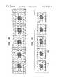
- FIGS. 8A-8Sshow views of a plurality of semiconductor chip packages in progressive steps in a manufacturing process according to one embodiment of the method of the present invention.
- FIGS. 8A, 8 B, 8 C, 8 Eare top plan view of such packages in various steps in such manufacturing process.
- FIG. 8Dis a top plan view of a component used in such manufacturing process.
- FIG. 8Fis a bottom plan view of another component used in such manufacturing process.
- FIG. 8Gis a top plan view of such packages after the component of FIG. 8F has been adhered to such packages.
- FIG. 8His a bottom plan view of the packages in progress after the manufacturing step described in FIG. 8G has been completed.
- FIG. 8Iis an exploded view of a portion of FIG. 8 H.
- FIG. 8Jis a bottom plan view of the packages in progress after another manufacturing process step has been completed.
- FIG. 8Kis an exploded view of a portion of FIG. 8 J.
- FIG. 8Lis a bottom plan view of another component used in such manufacturing process.
- FIG. 8Mis a bottom plan view of the packages in process after the component of FIG. 8L has been adhered to such packages.
- FIG. 8Nis a top plan view of another component used in such manufacturing process.
- FIG. 8Ois a top plan view of the packages in process after the component of FIG. 8N has been adhered to such packages.
- FIGS. 8P-8Sare bottom plan view of such packages in various steps in such manufacturing process.
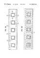
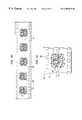
- the semiconductor chip assembly 1includes a semiconductor chip 2 , an expander ring 7 and a dielectric element 5 .
- Semiconductor chip 2has a face surface 15 , a back surface 16 opposite the face surface, and four side surfaces 17 (two of which are visible in FIG. 1) which connect the face surface to the back surface. The four side surfaces form the outer perimeter of semiconductor chip 2 .
- Expander ring 7has a first surface 20 , a second surface 21 opposite the first surface, and four inner side walls 22 (two of which are visible in FIG. 1) which define a central opening.
- Dielectric element 5has a top surface 18 , a bottom surface 19 opposite top surface 18 , and a plurality of apertures 6 .
- Top surface 18is comprised of a central region, which is disposed beneath the face surface 15 of semiconductor chip 2 , and a peripheral region that surrounds the central region. Descriptors such as “top”, “bottom”, “beneath”, etc, should be understood to refer to the drawing in FIG. 1 and not to any gravitational frame of reference.
- dielectric element 5is flexible. Expander ring 7 is disposed over dielectric element 5 such that second surface 21 confronts the peripheral region of the top surface 18 of dielectric element 5 .
- the CTE of the dielectric elementis preferably from 15 to 22 ppm/° C., inclusive.
- the CTE of the expander ringis preferably from 5 to 30 ppm/° C., inclusive.
- Semiconductor chip 2is disposed within the central opening of expander ring 7 such that a gap 8 is formed between the outer perimeter of semiconductor chip 2 and the four inner side walls 22 of the central opening of expander ring 7 .
- a compliant layer 11is disposed between face surface 15 of semiconductor chip 2 and top surface 18 of dielectric element 5 .
- the CTE of the compliant layeris preferably from 100 to 300 ppm/° C., inclusive.
- An adhesive 27is disposed between the expander ring 7 and the dielectric element 5 .
- An encapsulant 3is disposed within gap 8 . In preferred embodiments,
- the encapsulantis elastomeric, has a modulus of 0.5 to 600 MPa. and is comprised of a silicone gel, a silicone elastomer, a filled silicone elastomer, a urethane, an epoxy, or a flexiblized epoxy. In particularly preferred embodiments, the elastomeric encapsulant is comprised of a silicone elastomer.
- leads 4interconnect contacts on the semiconductor chip 2 to terminals on the dielectric element 5 .
- Leads 4may be formed by any method, including the methods disclosed in commonly assigned U.S. Pat. Nos. 5,390,844; 5,398,863; 5,489,749; 5,491,302; and 5,536,909, the disclosures of which are incorporated herein by reference. Leads 4 may also be formed by wire bonding. In preferred embodiments, the leads are comprised of gold, copper or alloys thereof or combinations thereof.
- the leads 4are used to electrically interconnect terminals on the dielectric element to contacts on the semiconductor chip or to electrically interconnect the terminals to an external circuit.
- the apertures 6may be used to provide access for a bonding tool to the leads so that such electrically interconnections can be made.
- the aperturesare optional and may be replaced with other means for making such electrical interconnections.
- One such meansis an electrically conductive path disposed within such dielectric element.
- compliant layer 11may include a plurality of compliant spacers 11 a .
- One or more such compliant spacers 11 amay also be disposed between second surface 21 of expander ring 7 and the peripheral region of top surface 18 of dielectric element 5 .
- Compliant spacers 11 apreferably have a modulus of 0.5 to 600 MPa.
- the compliant spacers 11 aare comprised of a silicone gel, a silicone elastomer or a flexiblized epoxy.
- the compliant spacersare comprised of a silicone elastomer.
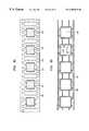
- a thermal spreader 10may be connected to back surface 16 of semiconductor chip 2 with a first adhesive 9 , as depicted in FIG. 3 .
- Thermal spreader 10may also be connected to the first surface 20 of expander ring 7 with a second adhesive or ring adhesive 26 .
- the second adhesivemay also be used to accommodate for differences and tolerances between the semiconductor chip and the expander ring.
- First adhesive 9 and second adhesive 26may be comprised of the same or different materials. In preferred embodiments, the first and second adhesives have a modulus between 0.5 to 600 MPa.
- the first and second adhesivesare preferably comprised of a silicone gel, a silicone elastomer, a polyimide siloxane, or a flexiblized epoxy.
- the first and second adhesivesmay further comprise one or more fillers. In preferred embodiments, at least one of such fillers has a high thermal conductivity. Such highly thermally conductive fillers may be metallic or non-metallic.
- the second adhesiveis comprised of a silicone elastomer.
- the preferred first adhesiveis selected from the group consisting of filled flexiblized epoxies and filled silicone elastomers. Filled flexiblized epoxies are particularly preferred.
- the preferred first adhesiveis selected from the group consisting of filled flexiblized epoxies, filled polyimide siloxanes and filled silicone elastomers.
- the preferred first adhesiveis an epoxy filled with silver/glass, an epoxy filled with gold/geranium alloys, or an epoxy filled with gold/silicon alloys.
- a plurality of compliant spacers 11 bmay be disposed between thermal spreader 10 and the first surface 20 of expander ring 7 .
- the compliant spacers 11 bare comprised of a silicone gel, a silicone elastomer or a flexiblized epoxy.
- the compliant spacersare comprised of a silicone elastomer.
- semiconductor chip 2is connected to dielectric element 5 with a compliant layer comprised of compliant spacers 11 a .
- Expander ring 7is connected to the peripheral region of the top surface 18 of dielectric element 5 with a plurality of compliant spacers 11 a and to thermal spreader 10 with a plurality of compliant spacers 11 b .
- Compliant spacers 11 a and 11 bmay have similar dimensions or, as depicted in FIG. 5, different dimensions.
- Compliant spacers 11 a and 11 bmay be comprised of the same or different materials.
- terminals 23 on the dielectric element 5may be disposed on the top surface 18 of the dielectric element 5 .
- Leads 4connect contacts (not shown) on semiconductor chip 2 with terminals 23 .
- a plated via 24 disposed in dielectric element 5is connected to each terminal 23 .
- An electrically conductive mass 13is disposed within each via 24 . In preferred embodiments each electrically conductive mass 13 is a solder ball.
- the semiconductor chip assembly 1 of the present inventionmay have both fan-in leads 4 a and fan-out leads 4 b .
- Dielectric element 5has apertures 6 which accommodate both fan-in leads 4 a and fan-out leads 4 b .
- the fan-in and fan-out leadsare arranged interstitially such that every other lead in a row of leads is a fan-in lead and the remaining leads are fan-out leads.
- Assembly 1also has a solder mask or coverlay 14 .
- Coverlay 14is disposed over the bottom surface 19 of dielectric element 5 .
- Coverlay 14has a plurality of holes 25 which are aligned with terminals 23 .
- Assembly 1further comprises a plurality of electrically conductive masses 13 which are disposed in such holes 25 . Masses 13 can be used to electrically and physically connect the assembly to an external circuit, such as a printed circuit board.
- the dielectric element described with reference to the above semiconductor chip packages and methods for making the samepreferably is a flexible dielectric element.
- the dielectric elementis a thin sheet of a polymeric material such as a polyimide, a fluoropolymer, a thermoplastic polymer, or an elastomer, with polyimide being a particularly preferred material for use as the flexible dielectric element.
- the flexible dielectric elementis from 10 to 100 microns and more preferably from 25 to 75 microns thick.
- Each expander ringis used to support the solder balls which are attached to the terminals of the fan-out leads and to add structural stability to the package.
- the strip of expander ringsmay be made of any material which will support the solder balls.
- the expander ringsmay be made a conductive or a non-conductive material.
- the expander ringsmay be made of a metal, a plastic, or a paper based material.
- the expander ringsare comprised of a material selected from alloy 42, copper, invar, steel, polypropylene, epoxy or paper phenolic, or alloys thereof, or combinations thereof.
- the expander ringsare comprised of a material selected from copper, copper alloys, steel and combinations thereof.
- the expander ringmay be thicker or thinner than the associated semiconductor chip. In preferred embodiments however, the thickness of the expander ring is less than or equal to the thickness of the semiconductor die.
- the CTE of the expander ringis preferably intermediate between the CTE of the semiconductor chip and the CTE of the dielectric element. If the package contains a thermal spreader, the CTE of the thermal spreader is preferably low, close to the CTE of the semiconductor chip, and the CTE of the expander ring is preferably intermediate between the CTE of the thermal spreader and the CTE of the dielectric: element. In preferred embodiments, the CTE of the thermal spreader is from 5 to 30 ppm/° C., inclusive.
- One or more capacitors, transistors, and/or resistorsmay be embedded in the expander ring and/or on the dielectric element and electrically connected, via wire bonds, solder or a conductive adhesive, to one or more terminals on the dielectric element.
- the thermal spreaderis made from a material having a high thermal conductivity.
- the CTE of the thermal spreaderis close to the CTE of the semiconductor chip.
- the thermal spreaderis preferably made from a material selected from the group consisting of copper, copper alloys, nickel plated copper alloys, aluminum, aluminum alloys, anodized aluminum alloys, and steel.
- the thermal spreaderis preferably made from a material selected from the group consisting of copper, copper alloys, alloy 42 and multi-layered laminates containing copper coated invar. The preferred multi-layer laminate is copper-invar-copper.
- the thermal spreaderis preferably made of a material selected from the group consisting of aluminum nitride and tungsten copper.
- the coverlaymay be a temporary coverlay or a permanent coverlay.
- the coverlay materialmust be capable of being bonded, at least temporarily, to the dielectric element and of sealing any apertures or holes in such element.
- the coverlayis preferably1 ⁇ 2 mil to 10 mils thick, more preferably 1 ⁇ 2 mil to 5 mils thick, most preferably less than 2.5 mils thick.
- the coverlay materialis preferably comprised of polypropylene, polyester, polyimide or combinations thereof, with polyimide being particularly preferred for use as a permanent coverlay and polypropylene being particularly preferred for applications using a temporary coverlay. Materials which are commonly used as solder masks, such as solder masks sold under Dupont's brand name Pyralux® may also be used as a coverlay.
- Dupont's Pyralux® solder maskare generally photoimageable, dry film solder masks which are based on acrylic, urethane and -imide based materials.
- the coverlaymay also comprise an adhesive layer.
- the adhesive layeris preferably comprised of an acrylic, epoxy or silicone adhesive, with acrylic adhesives being particularly preferred.
- the adhesive layerPrior to the step in which the coverlay is laminated to the dielectric element, the adhesive layer must be tacky or must be in a form that is heat and/or pressure activated.
- the coverlay used in the present inventionis a permanent coverlay.
- the coverlaymay have a plurality of apertures. If the coverlay is comprised of a photoimageable material, the apertures may be formed in the coverlay after it is attached to the dielectric element.
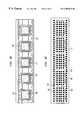
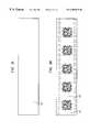
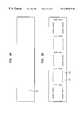
- FIGS. 8A-8Sdepict various steps in one method of the present invention.
- a dielectric element 101is provided.
- dielectric element 101is flexible.
- Dielectric element 101is in a strip form and has a top surface 102 , a bottom surface (not shown) opposite top surface 102 , and a plurality of apertures 104 .
- Apertures 104are sometimes also referred to as bond windows.
- the flexible dielectric element described with reference to the above semiconductor chip packages and methods for making the sameis preferably a thin sheet of a polymeric material such as a polyimide, a fluoropolymer, a thermoplastic polymer, or an elastomer, with polyimide being a particularly preferred material for use as the flexible dielectric element.
- the flexible dielectric elementis from 10 to 100 microns and more preferably from 25 to 75 microns thick.
- Polyimide in strip formis generally supplied with a plurality of sprocket holes 105 . Although such sprocket holes may be used as an alignment aid in the method of the present invention, such sprocket holes are not required to practice the present method.
- Flexible dielectric element 101has a plurality of electrically conductive traces 106 . Only a portion of each trace is visible through the bond windows 104 . Each trace 106 has a contact end and a terminal-end. The contact-end will eventually be connected to a contact on the face surface of semiconductor chip 108 . Neither the tip nor the terminal-ends are visible in FIG. 8 A. Traces 106 may be disposed on either the top surface 102 or the bottom surface 103 of the flexible dielectric element 101 . In the embodiment pictured in FIGS. 8A-8S, traces 106 are disposed on the bottom surface 103 (See FIG. 8 H).
- a plurality of compliant spacers 107are disposed on the top surface 102 of flexible dielectric element 101 .
- Some methods of disposing such compliant spacers or resilient elementsare described in commonly assigned U.S. Pat. No. 5,659,952 and U.S. patent application with Ser. No. 08/879,922 and a filing date of Jun. 20, 1997, the disclosures of which are incorporated herein by reference.
- the compliant spacers 107are comprised of a silicone gel, a silicone elastomer or a flexiblized epoxy.
- the compliant spacerspreferably have a modulus of 0.5 to 600 MPa.
- the compliant spacersare comprised of a silicone elastomer. Prior to die attach some or all of the compliant spacers 107 may be in an uncured, partially cured or fully cured state. An adhesive may be disposed on the top surface of such spacers 107 .
- Commonly assigned U.S. patent application with Ser. No. 08/931,680 and a filing date of Sep. 16, 1997, the disclosure of which is incorporated herein by reference,teaches one method of disposing an adhesive over a compliant spacer or compliant pad.
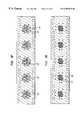
- a plurality of semiconductor chips 108are then disposed over the top surface 102 of flexible dielectric element 101 .
- Each chip 108has a face surface (not shown), a back surface 111 opposite the face surface, and a plurality of electrically conductive contacts (not shown) disposed on the face surface 110 .
- Each chip 108is positioned over one set of bond windows 104 and the face surface of each is adhered to flexible dielectric element 101 . If compliant spacers 107 are in an uncured state, a partially cured state, or have an adhesive disposed on the top surfaces of such spacers, chips 108 may be adhered to flexible dielectric element 101 using such spacers 107 . Heat and pressure may be required to achieve a good bond between spacers 107 and chips 108 .
- each expander ring 109has a first surface 112 , a second surface (not shown) opposite first surface 112 , and four inner side walls 113 which define a central opening 114 .
- Each expander ringis used to support the solder balls which are attached to the terminals of the fan-out leads and to add structural stability to the package.
- Various methods of packaging semiconductor chips using expander ringsare described in co-pending, commonly assigned U.S. patent application Ser. No. 09/067,310, having a filing date of Apr. 28, 1998, the disclosure of which is hereby w incorporated herein by reference.
- the expander rings of the '310 applicationare referred to as unitary support structures.
- the strip of expander rings 109may be made of any material which will support the solder balls.
- the expander ringsmay be made of a conductive or a non-conductive material.
- the expander ringsmay be made of a metal, a plastic, or a paper based material.
- the expander ringsare comprised of a material selected from alloy 42, copper, invar, steel, polypropylene, epoxy or paper phenolic, or alloys thereof, or combinations thereof.
- the expander ringsare comprised of a material selected from copper, copper alloys, steel and combinations thereof.
- the expander ringmay be thicker or thinner than the associated semiconductor chip. In preferred embodiments however, the thickness of the expander ring is less than or equal to the thickness of the semiconductor die.
- the CTE of the expander ringis preferably intermediate between the CTE of the semiconductor chip and the CTE of the flexible dielectric element. If the package contains a thermal spreader, the CTE of the thermal spreader is preferably low, close to the CTE of the semiconductor chip, and the CTE of the expander ring is preferably intermediate between the CTE of the thermal spreader and the CTE of the flexible dielectric element.
- One or more capacitors, resistors, and/or transistorsmay be embedded in the expander ring and electrically connected, via wire bonds, solder or a conductive adhesive, to one or more terminals on the flexible dielectric element.
- the strip of expander rings 109is disposed over the flexible dielectric element 101 such that a) the second surface of each expander ring 109 confronts the top surface 102 of the flexible dielectric element 101 ; b) the central opening 114 of each expander ring 109 is disposed around one of the semiconductor chips 108 ; and c) for each semiconductor chip 108 , a gap 115 is maintained between each inner side wall 113 and the outer perimeter of the semiconductor chip 108 .
- wis the width of gap 115 ;
- CTE expander ringis the coefficient of thermal expansion of the expander ring;
- CTE chipis the coefficient of thermal expansion of the semiconductor chip;
- X cis the shortest distance between the outer edge of the chip and the center of the chip;
- CTE encapsulantis the coefficient of thermal expansion of the encapsulant;
- pis the Poisson ratio for the encapsulant which will be disposed within the gap.
- Xcis not constant for all points on the outer edge of the chip.
- wcan be calculated for each point on the outer edge of the chip.
- the gap between the chip and the expander ring, as measured at each such point on the outer edge of the chipshould be at least the value of w calculated for that point.
- the width of the gapis constant and is selected to be at least as wide as the highest value of w calculated for the chip.
- the encapsulantis elastomeric.
- the elastomeric encapsulanthas a modulus of 0.5 to 600 MPa. and is comprised oF a silicone gel, a silicone elastomer, a filled silicone elastomer, a urethane, an epoxy, or a flexiblized epoxy.
- the elastomeric encapsulantis comprised of a silicone elastomer.
- the strip of expander rings 109may have one or more fidicuals to aid in the proper alignment of the expander rings on the flexible dielectric element.
- the sprocket holes 105may also be used to aid in the alignment of the expander rings.
- the second surface of each of the expander rings 109is adhered to the compliant spacers 107 , preferably using heat and/or pressure.
- the first surface 112 of each expander ring 109is coplanar with the back surface 111 of each semiconductor chip 108 .
- the second surface of the expander ringmay be coplanar with the face surface of each semiconductor chip 108 .
- Such heat and pressurecan also be used to correct for any lack of coplanarity between each expander ring 109 and the associated semiconductor chip 108 .
- a strip of thermal spreaders 116is provided.
- the strip of thermal spreaders 116has an alpha surface (not shown) and a beta surface 117 opposite the alpha surface.
- the thermal spreaderis made from a material having a high thermal conductivity.
- the CTE of the thermal spreaderis close to the CTE of the semiconductor chip.
- the thermal spreaderis preferably made from a material selected from the group consisting of copper, copper alloys, nickel plated copper alloys, aluminum, aluminum alloys, anodized aluminum alloys, and steel.
- the thermal spreaderis preferably made from a material selected from the group consisting of copper, copper alloys, alloy 42 and multi-layered laminates containing copper coated invar.
- the preferred multi-layer laminateis copper-invar-copper.
- the thermal spreaderis preferably made of a material selected from the group consisting of aluminum nitride and tungsten copper.
- the strip of thermal spreaders 116may have a plurality of elongated slots 119 . Such slots 119 are incorporated in the strip of thermal spreaders 116 to ease the singulation process in which the strip of packaged semiconductor chips are cut into individual packages.
- the strip of thermal spreaders 116may have one or more fiducials to aid in the alignment of the thermal spreaders.
- the strip of thermal spreadersmay be aligned with sprocket holes 105 in flexible dielectric element 101 to aid in the positioning of the thermal spreaders.
- a first adhesive 118is disposed on the beta surface 117 . Such adhesive may take for example, the form of a pad, a film or a dispensed pattern such as a plurality of dots of adhesive.
- Adhesive 118will eventually be used to bond beta surface 117 to the back surfaces of each of semiconductor chips 108 .
- a second adhesive or ring adhesive 118 ′may also be disposed on beta surface 117 and be in the form of a pad, a film or a plurality of dots. Second adhesive 118 may be used to accommodate for differences and tolerances between the semiconductor chip and the expander ring. The dots of adhesive 118 ′ will eventually be used to bond beta surface 117 to first surface 112 of each expander ring 109 . If the CTE of the strip of thermal spreaders 116 and the CTE of the semiconductor chips is not matched, then adhesive 118 should be compliant. In preferred embodiments, both adhesives 118 and 118 ′ are compliant.
- Adhesives 118 and 118 ′may be comprised of the same or different materials.
- the first and second adhesivesare comprised of a silicone gel, a silicone elastomer, a polyimide siloxane, or a flexiblized epoxy.
- the first and second adhesivemay further comprises one or more fillers. In preferred embodiments, at least one of such fillers has a high thermal conductivity. Such highly thermally conductive fillers may be metallic or non-metallic.
- the first and second adhesiveshave a modulus between 0.5 to 600 MPa. and are comprised of a silicone gel, a silicone elastomer, a polyimide siloxane, or a flexiblized epoxy.
- the second adhesiveis comprised of a silicone elastomer.
- the preferred first adhesiveis selected from the group consisting of filled flexiblized epoxies and filled silicone elastomers. Filled flexiblized epoxies are particularly preferred.
- the preferred first adhesiveis selected from the group consisting of filled flexiblized epoxies, filled polyimide siloxanes and filled silicone elastomers.
- the preferred first adhesiveis an epoxy filled with silver/glass, an epoxy filled with gold/geranium alloys, or an epoxy filled with gold/silicon alloys.
- the dimensions of the dots of adhesives 118 and 118 ′may be the same or different.
- the strip of thermal spreaders 116is disposed over semiconductor chips 108 and expander rings 109 such that the beta surface 117 of the strip of thermal spreaders 116 confronts the back surfaces 111 of semiconductor chips 108 and the first surfaces 112 of each expander ring 109 .
- the strip of thermal spreaders 116is adhered to such back surfaces and first surfaces with the adhesives 118 and 118 ′. Once this is complete, the alpha surface 120 of the strip of expander rings 109 is visible from a top plan view, as depicted in FIG. 8 G.
- FIG. 8His a view of the bottom surface 103 of the flexible dielectric element 101 prior to the processing step in which the leads are formed. A portion of the face surface 110 of each chip 108 is visible in FIG. 8 H through bond windows 104 .
- FIG. 8Halso depicts a plurality of electrically conductive traces 121 disposed on the bottom surface 103 of flexible dielectric element 101 .
- FIG. 8Iis an exploded view of a portion of FIG. 8H, depicting more details of traces 121 .
- Each trace 121has a terminal 122 and a contact-end 123 .
- Some of the traces 121have a terminal 122 that is disposed on a portion of flexible dielectric element 101 which lies underneath the face surface 110 of semiconductor chip 108 .
- Some traceswill eventually be formed into “fan-in” leads.
- Some of the traces(such as trace 121 ′) have a terminal 122 ′ that is disposed on a portion of the flexible dielectric element which lies underneath the second surface of expander ring 109 .
- Such traces 121 ′will eventually be formed into “fan-out” leads.
- the package depicted in FIG. 8Ihas a total of 26 traces. In preferred embodiments, the package will have 40 or more leads, more preferably 40 to 1000 leads.
- terminals 122 and 122 ′are disposed in ordered rows or an area array having a consistent pitch.
- the fan-in and fan-out leadsare comprised of gold, copper or alloys thereof or combinations thereof.
- FIG. 8Jdepicts the flexible dielectric element 101 and the plurality of chips 108 after the fan-in and fan-out leads have been formed.
- FIG. 8Kis an exploded view of a portion of FIG. 8 J.
- the contact-end 123 of each trace 121is bonded to an electrically conductive contact on the face surface 110 of semiconductor chip 108 to form a fan-in lead 124 which electrically interconnects the chip 108 to the flexible dielectric element 101 .
- the contact-end 123 ′ of each trace 121 ′is bonded to an electrically conductive contact on the face surface 110 of semiconductor chip 108 to form a fan-out lead 124 ′.
- the fan-in and fan-out leadsmay be formed by any method, including the methods disclosed in commonly assigned U.S. Pat. Nos. 5,390,844; 5,398,863; 5,489,749; 5,491,302; and 5,536,909, the disclosures of which are incorporated herein by reference.
- the fan-in and fan-out leadsmay be formed by wire bonding each contact to the respective terminal.
- coverlay 125which is depicted in FIG. 8 L.
- the coverlaymay be a temporary coverlay or a permanent coverlay.
- the coverlay materialmust be capable of being bonded, at least temporarily, to the flexible dielectric element and of sealing any apertures or holes in such element.
- the coverlayis preferably 1 ⁇ 2 mil to 10 mils thick, more preferably 1 ⁇ 2 mil to 5 mils thick, most preferably less than 2.5 mils thick.
- the coverlay materialis preferably comprised of polypropylene, polyester, polyimide or combinations thereof, with polyimide being particularly preferred for use as a permanent coverlay and polypropylene being particularly preferred for applications using a temporary coverlay. Materials which are commonly used as solder masks, such as solder masks sold under Dupont's brand name Pyralux® may also be used as a coverlay.
- Dupont's Pyralux® solder masksare generally photoimageable, dry film solder mask which are based on acrylic, urethane and -imide based materials.
- the coverlaymay also comprise an adhesive layer.
- the adhesive layeris preferably comprised of an acrylic, epoxy or silicone adhesive, with acrylic adhesives being particularly preferred.
- the adhesive layerPrior to the step in which the coverlay is laminated to the flexible dielectric element, the adhesive layer must be tacky or must be in an activatable form, such as a heat and/or pressure activated from.
- the coverlay used in the present inventionis a permanent coverlay.
- the coverlaymay have a plurality of apertures. If the coverlay is comprised of a photoimageable material, the apertures may be formed in the coverlay after it is attached to the flexible dielectric element.
- the coverlay depicted in FIG. 8Lis photoimageable and has been exposed in a pattern corresponding to the pattern of terminals on the flexible dielectric element.
- coverlay 125is laminated to the bottom surface 103 of flexible dielectric element 101 .
- the coverlaymay be vacuum laminated, pressure laminated, vacuum-pressure laminated or otherwise laminated onto the bottom surface 103 of the flexible dielectric element 101 .
- FIG. 8Mdepicts the bottom surface 103 after a transparent coverlay 125 has been laminated to it.
- a protective film 127is provided, as depicted in FIG. 8 N.
- the protective film of the present inventioncan be any of the materials listed above for the coverlay. In preferred embodiments, however, the protective film used in the present invention is a temporary coverlay which is removed after use.
- the protective filmmay be removed by, for example, using heat, peeling the film from the strip of thermal spreaders, or immersing the protective film in a caustic solution.
- Protective film 127is used to seal the elongated slots and any other apertures in thermal spreader 116 while a liquid composition is injected into the assembly to encapsulated it.
- Protective film 127should be capable of being bonded to the alpha surface of thermal spreader 116 .
- protective film 127may be removed after the encapsulation process, in preferred embodiments, protective film 127 forms only a temporary bond to the alpha surface of the strip of thermal spreaders 116 . As depicted in FIG. 8O, film 127 is adhered to the thermal spreader 116 to seal the elongated slots 119 .
- the assemblycan be encapsulated using a liquid composition which is curable to an encapsulant
- the encapsulantis elastomeric.
- the elastomeric encapsulantincreases the reliability of the assembly by compensating for the mismatch in CTE between the semiconductor chip package and an external circuit.
- the liquid compositionis disposed between the top surface 102 of the flexible dielectric element 101 and the thermal spreader 116 .
- the liquid compositionfills the open spaces between any of the expander ring, the thermal spreader, the semiconductor chip, the flexible dielectric element, the compliant adhesive, and the compliant spacers.
- the liquid compositionalso fills in gap 115 (see FIG. 8E) between the expander ring 109 and the semiconductor chip 108 .
- the assemblymay be encapsulated with the liquid composition via a dispensing operation, a dispensing operation followed by subjecting the assembly to vacuum and or pressure, a dispensing operation preformed while the assembly is under vacuum, or by a pressurized injection operation.
- Various methods of encapsulating the assemblyare disclosed, for example, in commonly assigned U.S. patent application Ser. No. 09/067,698 filed on Apr. 28, 1998.
- FIG. 8Pdepicts the assembly of the present invention after the strip has been vacuum impregnated with liquid composition 126 .
- Terminals 122 and 122 ′ and a portion of each lead 124 and 124 ′are visible in FIG. 8 P.
- the coverlay 125seals against the bottom surface 103 of the flexible dielectric element 101 to prevent the liquid encapsulant 126 from contaminating terminals 122 and 122 ′.
- liquid composition 126is cured or at least partially cured.
- Protective film 127may then removed from thermal spreader 116 . Holes are formed in coverlay 125 by exposing the photimageable coverlay to a developer, such as potassium carbonate.
- the holesare formed in a pattern corresponding to the pattern of terminals 122 and 122 ′ on flexible dielectric element 101 . Flux is then applied on the terminals and, as depicted in FIG. 8Q, solder balls 128 are disposed within the holes in coverlay 125 . The solder balls are reflowed.
- the plurality of semiconductor chips 108are then singulated as depicted in FIG. 8 R and FIG. 8S to form a plurality of packaged semiconductor chip assemblies 129 .
- FIGS. 8A-8Semploys various process steps which are conducted on components in strip format.
- the method of the present inventionmay also be practiced with components that are supplied in a reel to reel format.
Landscapes
- Engineering & Computer Science (AREA)
- Microelectronics & Electronic Packaging (AREA)
- Computer Hardware Design (AREA)
- Power Engineering (AREA)
- Physics & Mathematics (AREA)
- Condensed Matter Physics & Semiconductors (AREA)
- General Physics & Mathematics (AREA)
- Manufacturing & Machinery (AREA)
- Cooling Or The Like Of Semiconductors Or Solid State Devices (AREA)
Abstract
Description
Claims (14)
Priority Applications (2)
| Application Number | Priority Date | Filing Date | Title |
|---|---|---|---|
| US09/245,224US6309915B1 (en) | 1998-02-05 | 1999-02-05 | Semiconductor chip package with expander ring and method of making same |
| US09/950,132US6388340B2 (en) | 1998-02-05 | 2001-09-10 | Compliant semiconductor chip package with fan-out leads and method of making same |
Applications Claiming Priority (3)
| Application Number | Priority Date | Filing Date | Title |
|---|---|---|---|
| US7384398P | 1998-02-05 | 1998-02-05 | |
| US8437798P | 1998-05-06 | 1998-05-06 | |
| US09/245,224US6309915B1 (en) | 1998-02-05 | 1999-02-05 | Semiconductor chip package with expander ring and method of making same |
Related Child Applications (1)
| Application Number | Title | Priority Date | Filing Date |
|---|---|---|---|
| US09/950,132DivisionUS6388340B2 (en) | 1998-02-05 | 2001-09-10 | Compliant semiconductor chip package with fan-out leads and method of making same |
Publications (1)
| Publication Number | Publication Date |
|---|---|
| US6309915B1true US6309915B1 (en) | 2001-10-30 |
Family
ID=27372360
Family Applications (2)
| Application Number | Title | Priority Date | Filing Date |
|---|---|---|---|
| US09/245,224Expired - LifetimeUS6309915B1 (en) | 1998-02-05 | 1999-02-05 | Semiconductor chip package with expander ring and method of making same |
| US09/950,132Expired - LifetimeUS6388340B2 (en) | 1998-02-05 | 2001-09-10 | Compliant semiconductor chip package with fan-out leads and method of making same |
Family Applications After (1)
| Application Number | Title | Priority Date | Filing Date |
|---|---|---|---|
| US09/950,132Expired - LifetimeUS6388340B2 (en) | 1998-02-05 | 2001-09-10 | Compliant semiconductor chip package with fan-out leads and method of making same |
Country Status (1)
| Country | Link |
|---|---|
| US (2) | US6309915B1 (en) |
Cited By (57)
| Publication number | Priority date | Publication date | Assignee | Title |
|---|---|---|---|---|
| US20020180035A1 (en)* | 2001-06-04 | 2002-12-05 | Siliconware Precision Industries Co., Ltd. | Semiconductor package with heat sink |
| US6580165B1 (en)* | 2000-11-16 | 2003-06-17 | Fairchild Semiconductor Corporation | Flip chip with solder pre-plated leadframe including locating holes |
| US6586845B1 (en)* | 1998-10-28 | 2003-07-01 | Shinko Electric Industries Co., Ltd. | Semiconductor device module and a part thereof |
| US20030172257A1 (en)* | 2001-07-02 | 2003-09-11 | Globespan Virata Incorporated | Communications system using rings architecture |
| US6696319B2 (en)* | 2001-09-14 | 2004-02-24 | Infineon Technologies Ag | Method of attaching semiconductor devices on a switching device and such an attached device |
| US20040041254A1 (en)* | 2002-09-04 | 2004-03-04 | Lewis Long | Packaged microchip |
| US20040070068A1 (en)* | 2001-07-19 | 2004-04-15 | Makoto Yoshino | Semiconductor package insulation film and manufacturing method thereof |
| US6734045B2 (en)* | 1999-03-26 | 2004-05-11 | Hewlett-Packard Development Company, L.P. | Lossy RF shield for integrated circuits |
| US20040089930A1 (en)* | 2002-06-25 | 2004-05-13 | Tessera, Inc. | Simplified stacked chip assemblies |
| US6735865B2 (en)* | 2001-04-25 | 2004-05-18 | Benq Corporation | Flexible circuit board and method of fabricating the same |
| US20040112631A1 (en)* | 1999-07-08 | 2004-06-17 | Sunstar Giken Kabushiki Kaisha | Underfilling material for semiconductor package |
| US20040119143A1 (en)* | 2002-12-19 | 2004-06-24 | Karpman Maurice S. | Packaged microchip with isolator having selected modulus of elasticity |
| US6768646B1 (en) | 1998-01-23 | 2004-07-27 | Texas Instruments Incorporated | High density internal ball grid array integrated circuit package |
| US20040169272A1 (en)* | 1998-09-03 | 2004-09-02 | Hembree David R. | Chip on board with heat sink attachment and assembly |
| US6798048B2 (en)* | 2000-09-12 | 2004-09-28 | Mitsui Mining & Smelting Company, Ltd. | 2-Metal layer TAB tape and both-sided CSP•BGA tape |
| US6816385B1 (en)* | 2000-11-16 | 2004-11-09 | International Business Machines Corporation | Compliant laminate connector |
| US20040262749A1 (en)* | 2003-06-30 | 2004-12-30 | Matayabas J. Christopher | Wire-bonded package with electrically insulating wire encapsulant and thermally conductive overmold |
| US20050056870A1 (en)* | 2002-12-19 | 2005-03-17 | Karpman Maurice S. | Stress sensitive microchip with premolded-type package |
| US20050077618A1 (en)* | 2002-12-19 | 2005-04-14 | 3M Innovative Properties Company | Flexible heat sink |
| US20050090099A1 (en)* | 2002-01-19 | 2005-04-28 | Megic Corporation | Thin film semiconductor package and method of fabrication |
| US20050161780A1 (en)* | 2004-01-27 | 2005-07-28 | St Assembly Test Services Ltd. | Strip-fabricated flip chip in package and flip chip in system heat spreader assemblies and fabrication methods therefor |
| US7019410B1 (en)* | 1999-12-21 | 2006-03-28 | Micron Technology, Inc. | Die attach material for TBGA or flexible circuitry |
| US20060223229A1 (en)* | 2002-07-19 | 2006-10-05 | Asat Ltd. | Ball grid array package and process for manufacturing same |
| US20060238207A1 (en)* | 2005-04-21 | 2006-10-26 | Endicott Interconnect Technologies, Inc. | Interposer for use with test apparatus |
| US7166911B2 (en) | 2002-09-04 | 2007-01-23 | Analog Devices, Inc. | Packaged microchip with premolded-type package |
| US20070075726A1 (en)* | 2005-04-21 | 2007-04-05 | Endicott Interconnect Technologies, Inc. | Interposer and test assembly for testing electronic devices |
| US20070166554A1 (en)* | 2006-01-18 | 2007-07-19 | Ruchert Brian D | Thermal interconnect and interface systems, methods of production and uses thereof |
| US20080157298A1 (en)* | 2006-06-29 | 2008-07-03 | Analog Devices, Inc. | Stress Mitigation in Packaged Microchips |
| US20080265401A1 (en)* | 2001-12-31 | 2008-10-30 | Megica Corporation | Integrated chip package structure using organic substrate and method of manufacturing the same |
| US20090000428A1 (en)* | 2007-06-27 | 2009-01-01 | Siemens Medical Solution Usa, Inc. | Photo-Multiplier Tube Removal Tool |
| US20090093090A1 (en)* | 2007-10-04 | 2009-04-09 | Infineon Technologies Ag | Method for producing a power semiconductor module comprising surface-mountable flat external contacts |
| US20090250807A1 (en)* | 2006-11-14 | 2009-10-08 | Infineon Technologies Ag | Electronic Component and Method for its Production |
| US20090273075A1 (en)* | 2008-05-05 | 2009-11-05 | Infineon Technologies Ag | Semiconductor device and manufacturing of the semiconductor device |
| US20100013082A1 (en)* | 2006-08-11 | 2010-01-21 | Megica Corporation | Chip package and method for fabricating the same |
| US20100327429A1 (en)* | 2009-06-29 | 2010-12-30 | Ying-Te Ou | Semiconductor package structure and package method thereof |
| US7960272B2 (en) | 2002-10-24 | 2011-06-14 | Megica Corporation | Method for fabricating thermal compliant semiconductor chip wiring structure for chip scale packaging |
| US8021976B2 (en) | 2002-10-15 | 2011-09-20 | Megica Corporation | Method of wire bonding over active area of a semiconductor circuit |
| US8119446B2 (en) | 2001-12-31 | 2012-02-21 | Megica Corporation | Integrated chip package structure using metal substrate and method of manufacturing the same |
| US8148806B2 (en) | 2000-05-19 | 2012-04-03 | Megica Corporation | Multiple chips bonded to packaging structure with low noise and multiple selectable functions |
| US8168527B2 (en) | 2006-09-06 | 2012-05-01 | Megica Corporation | Semiconductor chip and method for fabricating the same |
| US8426982B2 (en) | 2001-03-30 | 2013-04-23 | Megica Corporation | Structure and manufacturing method of chip scale package |
| US8535976B2 (en) | 2001-12-31 | 2013-09-17 | Megica Corporation | Method for fabricating chip package with die and substrate |
| US9030029B2 (en) | 2001-12-31 | 2015-05-12 | Qualcomm Incorporated | Chip package with die and substrate |
| EP3026696A1 (en)* | 2014-11-26 | 2016-06-01 | STMicroelectronics Srl | Package for semiconductor devices sensitive to mechanical and thermo-mechanical stresses, such as mems pressure sensors |
| US20170084581A1 (en)* | 2015-09-17 | 2017-03-23 | Fujitsu Limited | Laminated chip, laminated-chip-mounted substrate and manufacturing method of laminated chip |
| US9676614B2 (en) | 2013-02-01 | 2017-06-13 | Analog Devices, Inc. | MEMS device with stress relief structures |
| US20180061795A1 (en)* | 2016-08-30 | 2018-03-01 | Samsung Electro-Mechanics Co., Ltd. | Fan-out semiconductor package |
| CN108807190A (en)* | 2013-02-21 | 2018-11-13 | 先进封装技术私人有限公司 | Semiconductor structure and its manufacturing method |
| US10131538B2 (en) | 2015-09-14 | 2018-11-20 | Analog Devices, Inc. | Mechanically isolated MEMS device |
| US20180366434A1 (en)* | 2017-06-16 | 2018-12-20 | Micron Technology, Inc. | Thermocompression bond tips and related apparatus and methods |
| US10167189B2 (en) | 2014-09-30 | 2019-01-01 | Analog Devices, Inc. | Stress isolation platform for MEMS devices |
| EP3723125A1 (en)* | 2019-04-08 | 2020-10-14 | ABB Schweiz AG | Power electronic module and method of manufacturing a power electronic module |
| US11410964B2 (en)* | 2019-11-22 | 2022-08-09 | Micron Technology, Inc. | Contaminant control in thermocompression bonding of semiconductors and associated systems and methods |
| US11417611B2 (en) | 2020-02-25 | 2022-08-16 | Analog Devices International Unlimited Company | Devices and methods for reducing stress on circuit components |
| US11434861B2 (en)* | 2018-08-06 | 2022-09-06 | Eldor Corporation S.P.A. | Ignition coil for an internal combustion engine and method for manufacturng the same |
| US20230138475A1 (en)* | 2021-10-28 | 2023-05-04 | Texas Instruments Incorporated | Isolated temperature sensor package with embedded spacer in dielectric opening |
| US11981560B2 (en) | 2020-06-09 | 2024-05-14 | Analog Devices, Inc. | Stress-isolated MEMS device comprising substrate having cavity and method of manufacture |
Families Citing this family (30)
| Publication number | Priority date | Publication date | Assignee | Title |
|---|---|---|---|---|
| KR100319624B1 (en)* | 1999-05-20 | 2002-01-09 | 김영환 | Semiconductor chip package and method for fabricating thereof |
| US6949824B1 (en)* | 2000-04-12 | 2005-09-27 | Micron Technology, Inc. | Internal package heat dissipator |
| US6469398B1 (en)* | 2001-03-29 | 2002-10-22 | Kabushiki Kaisha Toshiba | Semiconductor package and manufacturing method thereof |
| TW495943B (en) | 2001-04-18 | 2002-07-21 | Siliconware Precision Industries Co Ltd | Semiconductor package article with heat sink structure and its manufacture method |
| US6472741B1 (en)* | 2001-07-14 | 2002-10-29 | Siliconware Precision Industries Co., Ltd. | Thermally-enhanced stacked-die ball grid array semiconductor package and method of fabricating the same |
| US6555486B2 (en)* | 2001-07-12 | 2003-04-29 | Cool Shield, Inc. | Thermally conductive silk-screenable interface material |
| US6800948B1 (en)* | 2002-07-19 | 2004-10-05 | Asat Ltd. | Ball grid array package |
| US6979594B1 (en) | 2002-07-19 | 2005-12-27 | Asat Ltd. | Process for manufacturing ball grid array package |
| US20040124508A1 (en)* | 2002-11-27 | 2004-07-01 | United Test And Assembly Test Center Ltd. | High performance chip scale leadframe package and method of manufacturing the package |
| US7372151B1 (en) | 2003-09-12 | 2008-05-13 | Asat Ltd. | Ball grid array package and process for manufacturing same |
| US20050093181A1 (en)* | 2003-11-04 | 2005-05-05 | Brandenburg Scott D. | Heat sinkable package |
| US7091581B1 (en) | 2004-06-14 | 2006-08-15 | Asat Limited | Integrated circuit package and process for fabricating the same |
| US7411289B1 (en) | 2004-06-14 | 2008-08-12 | Asat Ltd. | Integrated circuit package with partially exposed contact pads and process for fabricating the same |
| US7390740B2 (en)* | 2004-09-02 | 2008-06-24 | Micron Technology, Inc. | Sloped vias in a substrate, spring-like contacts, and methods of making |
| TWI246759B (en)* | 2004-11-16 | 2006-01-01 | Siliconware Precision Industries Co Ltd | Heat dissipating package structure and fabrication method thereof |
| CN100435324C (en)* | 2004-12-20 | 2008-11-19 | 半导体元件工业有限责任公司 | Semiconductor package structure having enhanced thermal dissipation characteristics |
| US8610262B1 (en) | 2005-02-18 | 2013-12-17 | Utac Hong Kong Limited | Ball grid array package with improved thermal characteristics |
| US7523546B2 (en)* | 2005-05-04 | 2009-04-28 | Nokia Corporation | Method for manufacturing a composite layer for an electronic device |
| TWI334638B (en)* | 2005-12-30 | 2010-12-11 | Ind Tech Res Inst | Structure and process of chip package |
| TWI306296B (en)* | 2006-04-06 | 2009-02-11 | Siliconware Precision Industries Co Ltd | Semiconductor device with a heat sink and method for fabricating the same |
| CN101170118B (en)* | 2006-10-25 | 2010-11-10 | 鸿富锦精密工业(深圳)有限公司 | Image sensor encapsulation, image sensor module and their making method |
| US7830004B2 (en)* | 2006-10-27 | 2010-11-09 | Taiwan Semiconductor Manufacturing Company, Ltd. | Packaging with base layers comprising alloy 42 |
| KR101030769B1 (en)* | 2007-01-23 | 2011-04-27 | 삼성전자주식회사 | Stack Packages and Stack Packaging Methods |
| US8937372B2 (en)* | 2007-03-21 | 2015-01-20 | Stats Chippac Ltd. | Integrated circuit package system with molded strip protrusion |
| US7851906B2 (en)* | 2007-03-26 | 2010-12-14 | Endicott Interconnect Technologies, Inc. | Flexible circuit electronic package with standoffs |
| US7868445B2 (en)* | 2007-06-25 | 2011-01-11 | Epic Technologies, Inc. | Integrated structures and methods of fabrication thereof with fan-out metallization on a chips-first chip layer |
| US7800382B2 (en) | 2007-12-19 | 2010-09-21 | AEHR Test Ststems | System for testing an integrated circuit of a device and its method of use |
| US7968981B2 (en) | 2008-04-11 | 2011-06-28 | Stats Chippac Ltd. | Inline integrated circuit system |
| US8030957B2 (en) | 2009-03-25 | 2011-10-04 | Aehr Test Systems | System for testing an integrated circuit of a device and its method of use |
| US10796987B2 (en)* | 2018-11-06 | 2020-10-06 | Advanced Semiconductor Engineering, Inc. | Semiconductor device package and method of manufacturing the same |
Citations (11)
| Publication number | Priority date | Publication date | Assignee | Title |
|---|---|---|---|---|
| US5148265A (en) | 1990-09-24 | 1992-09-15 | Ist Associates, Inc. | Semiconductor chip assemblies with fan-in leads |
| US5148266A (en) | 1990-09-24 | 1992-09-15 | Ist Associates, Inc. | Semiconductor chip assemblies having interposer and flexible lead |
| US5258330A (en)* | 1990-09-24 | 1993-11-02 | Tessera, Inc. | Semiconductor chip assemblies with fan-in leads |
| US5455390A (en) | 1994-02-01 | 1995-10-03 | Tessera, Inc. | Microelectronics unit mounting with multiple lead bonding |
| US5477611A (en) | 1993-09-20 | 1995-12-26 | Tessera, Inc. | Method of forming interface between die and chip carrier |
| US5518964A (en) | 1994-07-07 | 1996-05-21 | Tessera, Inc. | Microelectronic mounting with multiple lead deformation and bonding |
| US5659952A (en) | 1994-09-20 | 1997-08-26 | Tessera, Inc. | Method of fabricating compliant interface for semiconductor chip |
| US5679977A (en) | 1990-09-24 | 1997-10-21 | Tessera, Inc. | Semiconductor chip assemblies, methods of making same and components for same |
| US5688716A (en)* | 1994-07-07 | 1997-11-18 | Tessera, Inc. | Fan-out semiconductor chip assembly |
| US6127724A (en) | 1996-10-31 | 2000-10-03 | Tessera, Inc. | Packaged microelectronic elements with enhanced thermal conduction |
| US6169328B1 (en)* | 1994-09-20 | 2001-01-02 | Tessera, Inc | Semiconductor chip assembly |
Family Cites Families (2)
| Publication number | Priority date | Publication date | Assignee | Title |
|---|---|---|---|---|
| US5760465A (en)* | 1996-02-01 | 1998-06-02 | International Business Machines Corporation | Electronic package with strain relief means |
| US5919329A (en)* | 1997-10-14 | 1999-07-06 | Gore Enterprise Holdings, Inc. | Method for assembling an integrated circuit chip package having at least one semiconductor device |
- 1999
- 1999-02-05USUS09/245,224patent/US6309915B1/ennot_activeExpired - Lifetime
- 2001
- 2001-09-10USUS09/950,132patent/US6388340B2/ennot_activeExpired - Lifetime
Patent Citations (11)
| Publication number | Priority date | Publication date | Assignee | Title |
|---|---|---|---|---|
| US5148265A (en) | 1990-09-24 | 1992-09-15 | Ist Associates, Inc. | Semiconductor chip assemblies with fan-in leads |
| US5148266A (en) | 1990-09-24 | 1992-09-15 | Ist Associates, Inc. | Semiconductor chip assemblies having interposer and flexible lead |
| US5258330A (en)* | 1990-09-24 | 1993-11-02 | Tessera, Inc. | Semiconductor chip assemblies with fan-in leads |
| US5679977A (en) | 1990-09-24 | 1997-10-21 | Tessera, Inc. | Semiconductor chip assemblies, methods of making same and components for same |
| US5477611A (en) | 1993-09-20 | 1995-12-26 | Tessera, Inc. | Method of forming interface between die and chip carrier |
| US5455390A (en) | 1994-02-01 | 1995-10-03 | Tessera, Inc. | Microelectronics unit mounting with multiple lead bonding |
| US5518964A (en) | 1994-07-07 | 1996-05-21 | Tessera, Inc. | Microelectronic mounting with multiple lead deformation and bonding |
| US5688716A (en)* | 1994-07-07 | 1997-11-18 | Tessera, Inc. | Fan-out semiconductor chip assembly |
| US5659952A (en) | 1994-09-20 | 1997-08-26 | Tessera, Inc. | Method of fabricating compliant interface for semiconductor chip |
| US6169328B1 (en)* | 1994-09-20 | 2001-01-02 | Tessera, Inc | Semiconductor chip assembly |
| US6127724A (en) | 1996-10-31 | 2000-10-03 | Tessera, Inc. | Packaged microelectronic elements with enhanced thermal conduction |
Cited By (130)
| Publication number | Priority date | Publication date | Assignee | Title |
|---|---|---|---|---|
| US6768646B1 (en) | 1998-01-23 | 2004-07-27 | Texas Instruments Incorporated | High density internal ball grid array integrated circuit package |
| US7244637B2 (en)* | 1998-09-03 | 2007-07-17 | Micron Technology, Inc. | Chip on board and heat sink attachment methods |
| US20040169272A1 (en)* | 1998-09-03 | 2004-09-02 | Hembree David R. | Chip on board with heat sink attachment and assembly |
| US6586845B1 (en)* | 1998-10-28 | 2003-07-01 | Shinko Electric Industries Co., Ltd. | Semiconductor device module and a part thereof |
| US8138079B2 (en) | 1998-12-21 | 2012-03-20 | Megica Corporation | Method of wire bonding over active area of a semiconductor circuit |
| US6734045B2 (en)* | 1999-03-26 | 2004-05-11 | Hewlett-Packard Development Company, L.P. | Lossy RF shield for integrated circuits |
| US20040112631A1 (en)* | 1999-07-08 | 2004-06-17 | Sunstar Giken Kabushiki Kaisha | Underfilling material for semiconductor package |
| US6881591B2 (en)* | 1999-07-08 | 2005-04-19 | Sunstar Suisse Sa | Underfilling material for semiconductor package |
| US20060197233A1 (en)* | 1999-12-21 | 2006-09-07 | Tongbi Jiang | Die attach material for TBGA or flexible circuitry |
| US20060103032A1 (en)* | 1999-12-21 | 2006-05-18 | Tongbi Jiang | Die attach material for TBGA or flexible circuitry |
| US7019410B1 (en)* | 1999-12-21 | 2006-03-28 | Micron Technology, Inc. | Die attach material for TBGA or flexible circuitry |
| US8148806B2 (en) | 2000-05-19 | 2012-04-03 | Megica Corporation | Multiple chips bonded to packaging structure with low noise and multiple selectable functions |
| US6798048B2 (en)* | 2000-09-12 | 2004-09-28 | Mitsui Mining & Smelting Company, Ltd. | 2-Metal layer TAB tape and both-sided CSP•BGA tape |
| US6890793B2 (en)* | 2000-11-16 | 2005-05-10 | Fairchild Semiconductor Corporation | Method for producing a semiconductor die package using leadframe with locating holes |
| US20030178717A1 (en)* | 2000-11-16 | 2003-09-25 | Fairchild Semiconductor Corporation | Flip chip with solder pre-plated leadframe including locating holes |
| US6816385B1 (en)* | 2000-11-16 | 2004-11-09 | International Business Machines Corporation | Compliant laminate connector |
| US6580165B1 (en)* | 2000-11-16 | 2003-06-17 | Fairchild Semiconductor Corporation | Flip chip with solder pre-plated leadframe including locating holes |
| US8426982B2 (en) | 2001-03-30 | 2013-04-23 | Megica Corporation | Structure and manufacturing method of chip scale package |
| US9018774B2 (en) | 2001-03-30 | 2015-04-28 | Qualcomm Incorporated | Chip package |
| US8912666B2 (en) | 2001-03-30 | 2014-12-16 | Qualcomm Incorporated | Structure and manufacturing method of chip scale package |
| US8748227B2 (en) | 2001-03-30 | 2014-06-10 | Megit Acquisition Corp. | Method of fabricating chip package |
| US6735865B2 (en)* | 2001-04-25 | 2004-05-18 | Benq Corporation | Flexible circuit board and method of fabricating the same |
| US20040123453A1 (en)* | 2001-04-25 | 2004-07-01 | Yi-Jing Leu | Method of forming a flexible circuit board |
| US6844622B2 (en)* | 2001-06-04 | 2005-01-18 | Siliconware Precision Industries Co., Ltd. | Semiconductor package with heat sink |
| US7074645B2 (en) | 2001-06-04 | 2006-07-11 | Siliconware Precision Industries Co., Ltd. | Fabrication method of semiconductor package with heat sink |
| US20020180035A1 (en)* | 2001-06-04 | 2002-12-05 | Siliconware Precision Industries Co., Ltd. | Semiconductor package with heat sink |
| US20050095875A1 (en)* | 2001-06-04 | 2005-05-05 | Chien-Ping Huang | Fabrication method of semiconductor package with heat sink |
| US20030204636A1 (en)* | 2001-07-02 | 2003-10-30 | Globespanvirata Incorporated | Communications system using rings architecture |
| US20030189940A1 (en)* | 2001-07-02 | 2003-10-09 | Globespan Virata Incorporated | Communications system using rings architecture |
| US20030172257A1 (en)* | 2001-07-02 | 2003-09-11 | Globespan Virata Incorporated | Communications system using rings architecture |
| US20030172189A1 (en)* | 2001-07-02 | 2003-09-11 | Globespanvirata Incorporated | Communications system using rings architecture |
| US20030191863A1 (en)* | 2001-07-02 | 2003-10-09 | Globespanvirata Incorporated | Communications system using rings architecture |
| US20030195991A1 (en)* | 2001-07-02 | 2003-10-16 | Globespanvirata Incorporated | Communications system using rings architecture |
| US7103008B2 (en) | 2001-07-02 | 2006-09-05 | Conexant, Inc. | Communications system using rings architecture |
| US20030196076A1 (en)* | 2001-07-02 | 2003-10-16 | Globespan Virata Incorporated | Communications system using rings architecture |
| US20030200343A1 (en)* | 2001-07-02 | 2003-10-23 | Globespan Virata Incorporated | Communications system using rings architecture |
| US20030200339A1 (en)* | 2001-07-02 | 2003-10-23 | Globespanvirata Incorporated | Communications system using rings architecture |
| US20030200342A1 (en)* | 2001-07-02 | 2003-10-23 | Globespan Virata Incorporated | Communications system using rings architecture |
| US20040070068A1 (en)* | 2001-07-19 | 2004-04-15 | Makoto Yoshino | Semiconductor package insulation film and manufacturing method thereof |
| US6894374B2 (en)* | 2001-07-19 | 2005-05-17 | Texas Instruments Incorporated | Semiconductor package insulation film and manufacturing method thereof |
| US6696319B2 (en)* | 2001-09-14 | 2004-02-24 | Infineon Technologies Ag | Method of attaching semiconductor devices on a switching device and such an attached device |
| US20080265401A1 (en)* | 2001-12-31 | 2008-10-30 | Megica Corporation | Integrated chip package structure using organic substrate and method of manufacturing the same |
| US9136246B2 (en) | 2001-12-31 | 2015-09-15 | Qualcomm Incorporated | Integrated chip package structure using silicon substrate and method of manufacturing the same |
| US8535976B2 (en) | 2001-12-31 | 2013-09-17 | Megica Corporation | Method for fabricating chip package with die and substrate |
| US8835221B2 (en) | 2001-12-31 | 2014-09-16 | Qualcomm Incorporated | Integrated chip package structure using ceramic substrate and method of manufacturing the same |
| US8471361B2 (en) | 2001-12-31 | 2013-06-25 | Megica Corporation | Integrated chip package structure using organic substrate and method of manufacturing the same |
| US8119446B2 (en) | 2001-12-31 | 2012-02-21 | Megica Corporation | Integrated chip package structure using metal substrate and method of manufacturing the same |
| US7898058B2 (en) | 2001-12-31 | 2011-03-01 | Megica Corporation | Integrated chip package structure using organic substrate and method of manufacturing the same |
| US9030029B2 (en) | 2001-12-31 | 2015-05-12 | Qualcomm Incorporated | Chip package with die and substrate |
| US20050090099A1 (en)* | 2002-01-19 | 2005-04-28 | Megic Corporation | Thin film semiconductor package and method of fabrication |
| US8492870B2 (en) | 2002-01-19 | 2013-07-23 | Megica Corporation | Semiconductor package with interconnect layers |
| US7977763B2 (en) | 2002-01-19 | 2011-07-12 | Megica Corporation | Chip package with die and substrate |
| US20050082658A1 (en)* | 2002-06-25 | 2005-04-21 | Tessera, Inc. | Simplified stacked chip assemblies |
| US20040089930A1 (en)* | 2002-06-25 | 2004-05-13 | Tessera, Inc. | Simplified stacked chip assemblies |
| US20060223229A1 (en)* | 2002-07-19 | 2006-10-05 | Asat Ltd. | Ball grid array package and process for manufacturing same |
| US7166911B2 (en) | 2002-09-04 | 2007-01-23 | Analog Devices, Inc. | Packaged microchip with premolded-type package |
| US20040041254A1 (en)* | 2002-09-04 | 2004-03-04 | Lewis Long | Packaged microchip |
| US8026588B2 (en) | 2002-10-15 | 2011-09-27 | Megica Corporation | Method of wire bonding over active area of a semiconductor circuit |
| US9153555B2 (en) | 2002-10-15 | 2015-10-06 | Qualcomm Incorporated | Method of wire bonding over active area of a semiconductor circuit |
| US8021976B2 (en) | 2002-10-15 | 2011-09-20 | Megica Corporation | Method of wire bonding over active area of a semiconductor circuit |
| US9142527B2 (en) | 2002-10-15 | 2015-09-22 | Qualcomm Incorporated | Method of wire bonding over active area of a semiconductor circuit |
| US8742580B2 (en) | 2002-10-15 | 2014-06-03 | Megit Acquisition Corp. | Method of wire bonding over active area of a semiconductor circuit |
| US7960272B2 (en) | 2002-10-24 | 2011-06-14 | Megica Corporation | Method for fabricating thermal compliant semiconductor chip wiring structure for chip scale packaging |
| US8334588B2 (en) | 2002-10-24 | 2012-12-18 | Megica Corporation | Circuit component with conductive layer structure |
| US20050056870A1 (en)* | 2002-12-19 | 2005-03-17 | Karpman Maurice S. | Stress sensitive microchip with premolded-type package |
| US6946742B2 (en)* | 2002-12-19 | 2005-09-20 | Analog Devices, Inc. | Packaged microchip with isolator having selected modulus of elasticity |
| US20050077618A1 (en)* | 2002-12-19 | 2005-04-14 | 3M Innovative Properties Company | Flexible heat sink |
| US7399919B2 (en)* | 2002-12-19 | 2008-07-15 | 3M Innovative Properties Company | Flexible heat sink |
| US20040119143A1 (en)* | 2002-12-19 | 2004-06-24 | Karpman Maurice S. | Packaged microchip with isolator having selected modulus of elasticity |
| US20040262749A1 (en)* | 2003-06-30 | 2004-12-30 | Matayabas J. Christopher | Wire-bonded package with electrically insulating wire encapsulant and thermally conductive overmold |
| US7141454B2 (en) | 2003-06-30 | 2006-11-28 | Intel Corporation | Wire-bonded package with electrically insulating wire encapsulant and thermally conductive overmold |
| US20080061447A1 (en)* | 2003-06-30 | 2008-03-13 | Matayabas J C Jr | Wire-bonded package with electrically insulating wire encapsulant and thermally conductive overmold |
| US7332797B2 (en) | 2003-06-30 | 2008-02-19 | Intel Corporation | Wire-bonded package with electrically insulating wire encapsulant and thermally conductive overmold |
| US20040266068A1 (en)* | 2003-06-30 | 2004-12-30 | Matayabas J. Christopher | Wire-bonded package with electrically insulating wire encapsulant and thermally conductive overmold |
| US20050161780A1 (en)* | 2004-01-27 | 2005-07-28 | St Assembly Test Services Ltd. | Strip-fabricated flip chip in package and flip chip in system heat spreader assemblies and fabrication methods therefor |
| US7153725B2 (en)* | 2004-01-27 | 2006-12-26 | St Assembly Test Services Ltd. | Strip-fabricated flip chip in package and flip chip in system heat spreader assemblies and fabrication methods therefor |
| US7511518B2 (en) | 2005-04-21 | 2009-03-31 | Endicott Interconnect Technologies, Inc. | Method of making an interposer |
| US20070075726A1 (en)* | 2005-04-21 | 2007-04-05 | Endicott Interconnect Technologies, Inc. | Interposer and test assembly for testing electronic devices |
| US20060238207A1 (en)* | 2005-04-21 | 2006-10-26 | Endicott Interconnect Technologies, Inc. | Interposer for use with test apparatus |
| US20080020566A1 (en)* | 2005-04-21 | 2008-01-24 | Endicott Interconnect Technologies, Inc. | Method of making an interposer |
| US7292055B2 (en) | 2005-04-21 | 2007-11-06 | Endicott Interconnect Technologies, Inc. | Interposer for use with test apparatus |
| US7501839B2 (en) | 2005-04-21 | 2009-03-10 | Endicott Interconnect Technologies, Inc. | Interposer and test assembly for testing electronic devices |
| WO2007084572A3 (en)* | 2006-01-18 | 2007-11-22 | Honeywell Int Inc | Thermal interconnect and interface systems, methods of production and uses thereof |
| US20070166554A1 (en)* | 2006-01-18 | 2007-07-19 | Ruchert Brian D | Thermal interconnect and interface systems, methods of production and uses thereof |
| US20090230521A2 (en)* | 2006-06-29 | 2009-09-17 | Analog Devices, Inc. | Stress Mitigation in Packaged Microchips |
| US20100013067A9 (en)* | 2006-06-29 | 2010-01-21 | Analog Devices, Inc. | Stress Mitigation in Packaged Microchips |
| US20080157298A1 (en)* | 2006-06-29 | 2008-07-03 | Analog Devices, Inc. | Stress Mitigation in Packaged Microchips |
| US8344487B2 (en) | 2006-06-29 | 2013-01-01 | Analog Devices, Inc. | Stress mitigation in packaged microchips |
| US9899284B2 (en) | 2006-08-11 | 2018-02-20 | Qualcomm Incorporated | Chip package and method for fabricating the same |
| US11031310B2 (en) | 2006-08-11 | 2021-06-08 | Qualcomm Incorporated | Chip package |
| US9391021B2 (en) | 2006-08-11 | 2016-07-12 | Qualcomm Incorporated | Chip package and method for fabricating the same |
| US20100013082A1 (en)* | 2006-08-11 | 2010-01-21 | Megica Corporation | Chip package and method for fabricating the same |
| US8168527B2 (en) | 2006-09-06 | 2012-05-01 | Megica Corporation | Semiconductor chip and method for fabricating the same |
| US20090250807A1 (en)* | 2006-11-14 | 2009-10-08 | Infineon Technologies Ag | Electronic Component and Method for its Production |
| US8049311B2 (en)* | 2006-11-14 | 2011-11-01 | Infineon Technologies Ag | Electronic component and method for its production |
| US20090000428A1 (en)* | 2007-06-27 | 2009-01-01 | Siemens Medical Solution Usa, Inc. | Photo-Multiplier Tube Removal Tool |
| US7955901B2 (en)* | 2007-10-04 | 2011-06-07 | Infineon Technologies Ag | Method for producing a power semiconductor module comprising surface-mountable flat external contacts |
| US20090093090A1 (en)* | 2007-10-04 | 2009-04-09 | Infineon Technologies Ag | Method for producing a power semiconductor module comprising surface-mountable flat external contacts |
| US20090273075A1 (en)* | 2008-05-05 | 2009-11-05 | Infineon Technologies Ag | Semiconductor device and manufacturing of the semiconductor device |
| US8669175B2 (en) | 2008-05-05 | 2014-03-11 | Infineon Technologies Ag | Semiconductor device and manufacturing of the semiconductor device |
| US8264085B2 (en)* | 2008-05-05 | 2012-09-11 | Infineon Technologies Ag | Semiconductor device package interconnections |
| CN101582396A (en)* | 2008-05-05 | 2009-11-18 | 英飞凌科技股份有限公司 | Semiconductor device and manufacturing of the same |
| DE102009018396B4 (en)* | 2008-05-05 | 2014-10-23 | Infineon Technologies Ag | Semiconductor device and manufacture of the semiconductor device |
| US8222707B2 (en)* | 2009-06-29 | 2012-07-17 | Advanced Semiconductor Engineering, Inc. | Semiconductor package structure and package method thereof |
| US20100327429A1 (en)* | 2009-06-29 | 2010-12-30 | Ying-Te Ou | Semiconductor package structure and package method thereof |
| US9676614B2 (en) | 2013-02-01 | 2017-06-13 | Analog Devices, Inc. | MEMS device with stress relief structures |
| CN108807190A (en)* | 2013-02-21 | 2018-11-13 | 先进封装技术私人有限公司 | Semiconductor structure and its manufacturing method |
| US10167189B2 (en) | 2014-09-30 | 2019-01-01 | Analog Devices, Inc. | Stress isolation platform for MEMS devices |
| US10759659B2 (en) | 2014-09-30 | 2020-09-01 | Analog Devices, Inc. | Stress isolation platform for MEMS devices |
| US9841341B2 (en) | 2014-11-26 | 2017-12-12 | Stmicroelectronics S.R.L. | Package for semiconductor devices sensitive to mechanical and thermo-mechanical stresses, such as MEMS pressure sensors |
| EP3026696A1 (en)* | 2014-11-26 | 2016-06-01 | STMicroelectronics Srl | Package for semiconductor devices sensitive to mechanical and thermo-mechanical stresses, such as mems pressure sensors |
| US10131538B2 (en) | 2015-09-14 | 2018-11-20 | Analog Devices, Inc. | Mechanically isolated MEMS device |
| US20170084581A1 (en)* | 2015-09-17 | 2017-03-23 | Fujitsu Limited | Laminated chip, laminated-chip-mounted substrate and manufacturing method of laminated chip |
| US10157868B2 (en)* | 2016-08-30 | 2018-12-18 | Samsung Electro-Mechanics Co., Ltd. | Fan-out semiconductor package |
| US10515916B2 (en) | 2016-08-30 | 2019-12-24 | Samsung Electronics Co., Ltd. | Fan-out semiconductor package |
| US20180061795A1 (en)* | 2016-08-30 | 2018-03-01 | Samsung Electro-Mechanics Co., Ltd. | Fan-out semiconductor package |
| US11705425B2 (en)* | 2017-06-16 | 2023-07-18 | Micron Technology, Inc. | Thermocompression bond tips and related apparatus and methods |
| US20210233887A1 (en)* | 2017-06-16 | 2021-07-29 | Micron Technology, Inc. | Thermocompression bond tips and related apparatus and methods |
| US20180366434A1 (en)* | 2017-06-16 | 2018-12-20 | Micron Technology, Inc. | Thermocompression bond tips and related apparatus and methods |
| US11024595B2 (en)* | 2017-06-16 | 2021-06-01 | Micron Technology, Inc. | Thermocompression bond tips and related apparatus and methods |
| US11434861B2 (en)* | 2018-08-06 | 2022-09-06 | Eldor Corporation S.P.A. | Ignition coil for an internal combustion engine and method for manufacturng the same |
| EP3723125A1 (en)* | 2019-04-08 | 2020-10-14 | ABB Schweiz AG | Power electronic module and method of manufacturing a power electronic module |
| US20220320037A1 (en)* | 2019-11-22 | 2022-10-06 | Micron Technology, Inc. | Contaminant control in thermocompression bonding of semiconductors and associated systems and methods |
| US11410964B2 (en)* | 2019-11-22 | 2022-08-09 | Micron Technology, Inc. | Contaminant control in thermocompression bonding of semiconductors and associated systems and methods |
| US11908828B2 (en)* | 2019-11-22 | 2024-02-20 | Micron Technology, Inc. | Contaminant control in thermocompression bonding of semiconductors and associated systems and methods |
| US11417611B2 (en) | 2020-02-25 | 2022-08-16 | Analog Devices International Unlimited Company | Devices and methods for reducing stress on circuit components |
| US12300631B2 (en) | 2020-02-25 | 2025-05-13 | Analog Devices International Unlimited Company | Devices and methods for reducing stress on circuit components |
| US11981560B2 (en) | 2020-06-09 | 2024-05-14 | Analog Devices, Inc. | Stress-isolated MEMS device comprising substrate having cavity and method of manufacture |
| US20230138475A1 (en)* | 2021-10-28 | 2023-05-04 | Texas Instruments Incorporated | Isolated temperature sensor package with embedded spacer in dielectric opening |
| US11879790B2 (en)* | 2021-10-28 | 2024-01-23 | Texas Instruments Incorporated | Isolated temperature sensor package with embedded spacer in dielectric opening |
Also Published As
| Publication number | Publication date |
|---|---|
| US6388340B2 (en) | 2002-05-14 |
| US20020006718A1 (en) | 2002-01-17 |
Similar Documents
| Publication | Publication Date | Title |
|---|---|---|
| US6309915B1 (en) | Semiconductor chip package with expander ring and method of making same | |
| US6521480B1 (en) | Method for making a semiconductor chip package | |
| EP3288077B1 (en) | Microelectronic package having a bumpless laminated interconnection layer | |
| US6020629A (en) | Stacked semiconductor package and method of fabrication | |
| US7408260B2 (en) | Microelectronic assemblies having compliant layers | |
| US6211572B1 (en) | Semiconductor chip package with fan-in leads | |
| US5843808A (en) | Structure and method for automated assembly of a tab grid array package | |
| CN100382260C (en) | Manufacturing method of semiconductor package | |
| US5866949A (en) | Chip scale ball grid array for integrated circuit packaging | |
| US6518089B2 (en) | Flip chip semiconductor device in a molded chip scale package (CSP) and method of assembly | |
| US5990545A (en) | Chip scale ball grid array for integrated circuit package | |
| US6927095B2 (en) | Low cost and compliant microelectronic packages for high I/O and fine pitch | |
| US20030207499A1 (en) | Compliant integrated circuit package | |
| KR100702968B1 (en) | Semiconductor package having a floating heat sink, laminated package using the same, and manufacturing method thereof | |
| EP1035577A1 (en) | Wiring substrate, method of manufacture thereof, and semiconductor device | |
| CN113035830A (en) | Semiconductor structure and manufacturing method thereof |
Legal Events
| Date | Code | Title | Description |
|---|---|---|---|
| AS | Assignment | Owner name:TESSERA, INC., A CORP. OF DELAWARE, CALIFORNIA Free format text:ASSIGNMENT OF ASSIGNORS INTEREST;ASSIGNOR:DISTEFANO, THOMAS H.;REEL/FRAME:009913/0285 Effective date:19990406 | |
| STCF | Information on status: patent grant | Free format text:PATENTED CASE | |
| CC | Certificate of correction | ||
| AS | Assignment | Owner name:FREESCALE SEMICONDUCTOR, INC., TEXAS Free format text:ASSIGNMENT OF ASSIGNORS INTEREST;ASSIGNOR:MOTOROLA, INC.;REEL/FRAME:015698/0657 Effective date:20040404 | |
| FPAY | Fee payment | Year of fee payment:4 | |
| AS | Assignment | Owner name:FREESCALE SEMICONDUCTOR, INC., TEXAS Free format text:ASSIGNMENT OF ASSIGNORS INTEREST;ASSIGNOR:MOTOROLA, INC.;REEL/FRAME:017198/0515 Effective date:20040404 | |
| FPAY | Fee payment | Year of fee payment:8 | |
| FPAY | Fee payment | Year of fee payment:12 | |
| AS | Assignment | Owner name:ROYAL BANK OF CANADA, AS COLLATERAL AGENT, CANADA Free format text:SECURITY INTEREST;ASSIGNORS:INVENSAS CORPORATION;TESSERA, INC.;TESSERA ADVANCED TECHNOLOGIES, INC.;AND OTHERS;REEL/FRAME:040797/0001 Effective date:20161201 | |
| AS | Assignment | Owner name:FOTONATION CORPORATION (F/K/A DIGITALOPTICS CORPORATION AND F/K/A DIGITALOPTICS CORPORATION MEMS), CALIFORNIA Free format text:RELEASE BY SECURED PARTY;ASSIGNOR:ROYAL BANK OF CANADA;REEL/FRAME:052920/0001 Effective date:20200601 Owner name:IBIQUITY DIGITAL CORPORATION, MARYLAND Free format text:RELEASE BY SECURED PARTY;ASSIGNOR:ROYAL BANK OF CANADA;REEL/FRAME:052920/0001 Effective date:20200601 Owner name:DTS, INC., CALIFORNIA Free format text:RELEASE BY SECURED PARTY;ASSIGNOR:ROYAL BANK OF CANADA;REEL/FRAME:052920/0001 Effective date:20200601 Owner name:INVENSAS BONDING TECHNOLOGIES, INC. (F/K/A ZIPTRONIX, INC.), CALIFORNIA Free format text:RELEASE BY SECURED PARTY;ASSIGNOR:ROYAL BANK OF CANADA;REEL/FRAME:052920/0001 Effective date:20200601 Owner name:TESSERA ADVANCED TECHNOLOGIES, INC, CALIFORNIA Free format text:RELEASE BY SECURED PARTY;ASSIGNOR:ROYAL BANK OF CANADA;REEL/FRAME:052920/0001 Effective date:20200601 Owner name:DTS LLC, CALIFORNIA Free format text:RELEASE BY SECURED PARTY;ASSIGNOR:ROYAL BANK OF CANADA;REEL/FRAME:052920/0001 Effective date:20200601 Owner name:TESSERA, INC., CALIFORNIA Free format text:RELEASE BY SECURED PARTY;ASSIGNOR:ROYAL BANK OF CANADA;REEL/FRAME:052920/0001 Effective date:20200601 Owner name:INVENSAS CORPORATION, CALIFORNIA Free format text:RELEASE BY SECURED PARTY;ASSIGNOR:ROYAL BANK OF CANADA;REEL/FRAME:052920/0001 Effective date:20200601 Owner name:PHORUS, INC., CALIFORNIA Free format text:RELEASE BY SECURED PARTY;ASSIGNOR:ROYAL BANK OF CANADA;REEL/FRAME:052920/0001 Effective date:20200601 |