US6309528B1 - Sequential electrodeposition of metals using modulated electric fields for manufacture of circuit boards having features of different sizes - Google Patents
Sequential electrodeposition of metals using modulated electric fields for manufacture of circuit boards having features of different sizesDownload PDFInfo
- Publication number
- US6309528B1 US6309528B1US09/419,881US41988199AUS6309528B1US 6309528 B1US6309528 B1US 6309528B1US 41988199 AUS41988199 AUS 41988199AUS 6309528 B1US6309528 B1US 6309528B1
- Authority
- US
- United States
- Prior art keywords
- pulses
- cathodic
- anodic
- duty cycle
- hydrodynamically
- Prior art date
- Legal status (The legal status is an assumption and is not a legal conclusion. Google has not performed a legal analysis and makes no representation as to the accuracy of the status listed.)
- Expired - Lifetime
Links
Images


Classifications
- H—ELECTRICITY
- H05—ELECTRIC TECHNIQUES NOT OTHERWISE PROVIDED FOR
- H05K—PRINTED CIRCUITS; CASINGS OR CONSTRUCTIONAL DETAILS OF ELECTRIC APPARATUS; MANUFACTURE OF ASSEMBLAGES OF ELECTRICAL COMPONENTS
- H05K3/00—Apparatus or processes for manufacturing printed circuits
- H05K3/40—Forming printed elements for providing electric connections to or between printed circuits
- H05K3/42—Plated through-holes or plated via connections
- H05K3/423—Plated through-holes or plated via connections characterised by electroplating method
- C—CHEMISTRY; METALLURGY
- C25—ELECTROLYTIC OR ELECTROPHORETIC PROCESSES; APPARATUS THEREFOR
- C25D—PROCESSES FOR THE ELECTROLYTIC OR ELECTROPHORETIC PRODUCTION OF COATINGS; ELECTROFORMING; APPARATUS THEREFOR
- C25D5/00—Electroplating characterised by the process; Pretreatment or after-treatment of workpieces
- C25D5/18—Electroplating using modulated, pulsed or reversing current
- C—CHEMISTRY; METALLURGY
- C25—ELECTROLYTIC OR ELECTROPHORETIC PROCESSES; APPARATUS THEREFOR
- C25D—PROCESSES FOR THE ELECTROLYTIC OR ELECTROPHORETIC PRODUCTION OF COATINGS; ELECTROFORMING; APPARATUS THEREFOR
- C25D5/00—Electroplating characterised by the process; Pretreatment or after-treatment of workpieces
- C25D5/60—Electroplating characterised by the structure or texture of the layers
- C25D5/605—Surface topography of the layers, e.g. rough, dendritic or nodular layers
- C25D5/611—Smooth layers
- H—ELECTRICITY
- H05—ELECTRIC TECHNIQUES NOT OTHERWISE PROVIDED FOR
- H05K—PRINTED CIRCUITS; CASINGS OR CONSTRUCTIONAL DETAILS OF ELECTRIC APPARATUS; MANUFACTURE OF ASSEMBLAGES OF ELECTRICAL COMPONENTS
- H05K2201/00—Indexing scheme relating to printed circuits covered by H05K1/00
- H05K2201/09—Shape and layout
- H05K2201/09209—Shape and layout details of conductors
- H05K2201/095—Conductive through-holes or vias
- H05K2201/09563—Metal filled via
- H—ELECTRICITY
- H05—ELECTRIC TECHNIQUES NOT OTHERWISE PROVIDED FOR
- H05K—PRINTED CIRCUITS; CASINGS OR CONSTRUCTIONAL DETAILS OF ELECTRIC APPARATUS; MANUFACTURE OF ASSEMBLAGES OF ELECTRICAL COMPONENTS
- H05K2203/00—Indexing scheme relating to apparatus or processes for manufacturing printed circuits covered by H05K3/00
- H05K2203/14—Related to the order of processing steps
- H05K2203/1476—Same or similar kind of process performed in phases, e.g. coarse patterning followed by fine patterning
- H—ELECTRICITY
- H05—ELECTRIC TECHNIQUES NOT OTHERWISE PROVIDED FOR
- H05K—PRINTED CIRCUITS; CASINGS OR CONSTRUCTIONAL DETAILS OF ELECTRIC APPARATUS; MANUFACTURE OF ASSEMBLAGES OF ELECTRICAL COMPONENTS
- H05K2203/00—Indexing scheme relating to apparatus or processes for manufacturing printed circuits covered by H05K3/00
- H05K2203/14—Related to the order of processing steps
- H05K2203/1492—Periodical treatments, e.g. pulse plating of through-holes
- H—ELECTRICITY
- H05—ELECTRIC TECHNIQUES NOT OTHERWISE PROVIDED FOR
- H05K—PRINTED CIRCUITS; CASINGS OR CONSTRUCTIONAL DETAILS OF ELECTRIC APPARATUS; MANUFACTURE OF ASSEMBLAGES OF ELECTRICAL COMPONENTS
- H05K3/00—Apparatus or processes for manufacturing printed circuits
- H05K3/46—Manufacturing multilayer circuits
- H05K3/4644—Manufacturing multilayer circuits by building the multilayer layer by layer, i.e. build-up multilayer circuits
- Y—GENERAL TAGGING OF NEW TECHNOLOGICAL DEVELOPMENTS; GENERAL TAGGING OF CROSS-SECTIONAL TECHNOLOGIES SPANNING OVER SEVERAL SECTIONS OF THE IPC; TECHNICAL SUBJECTS COVERED BY FORMER USPC CROSS-REFERENCE ART COLLECTIONS [XRACs] AND DIGESTS
- Y10—TECHNICAL SUBJECTS COVERED BY FORMER USPC
- Y10S—TECHNICAL SUBJECTS COVERED BY FORMER USPC CROSS-REFERENCE ART COLLECTIONS [XRACs] AND DIGESTS
- Y10S205/00—Electrolysis: processes, compositions used therein, and methods of preparing the compositions
- Y10S205/92—Electrolytic coating of circuit board or printed circuit, other than selected area coating
- Y—GENERAL TAGGING OF NEW TECHNOLOGICAL DEVELOPMENTS; GENERAL TAGGING OF CROSS-SECTIONAL TECHNOLOGIES SPANNING OVER SEVERAL SECTIONS OF THE IPC; TECHNICAL SUBJECTS COVERED BY FORMER USPC CROSS-REFERENCE ART COLLECTIONS [XRACs] AND DIGESTS
- Y10—TECHNICAL SUBJECTS COVERED BY FORMER USPC
- Y10T—TECHNICAL SUBJECTS COVERED BY FORMER US CLASSIFICATION
- Y10T428/00—Stock material or miscellaneous articles
- Y10T428/12—All metal or with adjacent metals
- Y10T428/12389—All metal or with adjacent metals having variation in thickness
- Y10T428/12396—Discontinuous surface component
- Y—GENERAL TAGGING OF NEW TECHNOLOGICAL DEVELOPMENTS; GENERAL TAGGING OF CROSS-SECTIONAL TECHNOLOGIES SPANNING OVER SEVERAL SECTIONS OF THE IPC; TECHNICAL SUBJECTS COVERED BY FORMER USPC CROSS-REFERENCE ART COLLECTIONS [XRACs] AND DIGESTS
- Y10—TECHNICAL SUBJECTS COVERED BY FORMER USPC
- Y10T—TECHNICAL SUBJECTS COVERED BY FORMER US CLASSIFICATION
- Y10T428/00—Stock material or miscellaneous articles
- Y10T428/31504—Composite [nonstructural laminate]
- Y10T428/31678—Of metal
Definitions
- This inventionrelates to electrodeposition of metals and more particularly to electrochemical metallization of substrates having surface features of different transverse dimensions.
- Electronic devicessuch as computers, cellular telephones, electronic entertainment devices, and the like, have long been manufactured by mounting components on circuit boards having electrically conductive traces thereon to interconnect the components.
- VLSIvery large scale integration
- ULSIultra large scale integration
- the interconnectionshave conventionally been provided by circuit boards having electrical conductors prepared by so called “printed wiring” techniques that involve masking, etching, and plating of conductive metal, usually copper, to provide the interconnects between chip modules or sockets designed to hold such modules.
- These “printed wiring boards”have typically been used to interconnect chips of conventional sizes.
- the chips or socketare mounted on the surface of the board with terminals fitted into holes through the board.
- the holesare typically lined with a thin layer of copper that is integral with the traces of copper on the surface of the board.
- the terminals of the chips or socketsare soldered to the copper layer lining the holes and thereby interconnected through the copper traces.
- the PWBsmay have copper traces on both sides as well as more than one inner layer of copper traces. Connections between copper traces in the different layers of these double-sided and multileyered PWBs are also provided by copper-lined holes passing through the board, commonly known as plated through-holes (PTHs).
- PTHsplated through-holes
- the copper lining in such holesis typically applied electrolytically, by first laying down a thin layer of electroless copper to provide electrical continuity and then electroplating copper to a thickness of a few mils to provide the connecting layer. While the copper could be applied solely using the electroless process, the processing time for the electroless process is significantly greater than the processing time for the electrolytic process.
- the holes in the PWBstypically are at least 12-13 mils in diameter. Because of the well-known problem of depositing metal electrolytically in recesses, special techniques have to be used to assure that a uniform layer of conductive metal is deposited in the holes.
- MCMsmultichip modules
- the holesare typically of smaller diameter than those of conventional PWBs, and may range from about 25 micrometers (1 mil) to about 250 micrometers (10 mils).
- Such holesare also effectively blind holes and the conductor deposition step provides the electrical contact to the terminal pads on the semiconductor devices as well as the interconnections between the devices.
- HDIhigh density interconnect
- Other names for this emerging technologyincludes built-up boards and micro via boards. Other designs for these build up boards involves adding the chip subsequent to processing.
- circuit boards having areas of high-density interconnections between micro via layers on either side of the PWB and conventional PWB layers or to semiconductor devicesalso must have structures adapted to connect the HDI board to other boards or peripheral devices.
- Such external connections to devices of conventional sizeare generally made using conventional PWB techniques, e.g., using plated-through holes.
- a single circuit board level or layermay include both areas of high-density interconnects and areas of conventional PWB connections.
- the electroplating conditions suitable for fabricating plated-through holesare not effective to deposit metal into the smaller blind holes and vias found in the HDI areas of the board.
- the conventional procedure for manufacture of such boardshas been to mask either the HDI area or the conventional PTH area of the board and plate each area under conditions appropriate for the size of the holes and recesses in the board.
- the full build electroless approachis utilized with the concomitant lengthy processing time and slow throughput.
- the conditionshave included special additives in the plating bath to improve the throwing power in order to promote the deposition of metal in the recesses, vias and holes.
- the requirement for masking certain areas of the board surfacehas introduced a number of processing steps, such as applying a photoresist layer, imaging the layer, developing the photoresist, and at least two separate electroplating steps, possibly in baths of different compositions.
- Deposition of conductive metal into the small, blind holes or vias used in HDIhas presented particular problems.
- Conventional metallization proceduressuch as chemical vapor deposition or physical vapor deposition as well as electroless deposition, are slow and expensive.
- Electroplating into small blind vias using conventional procedureshas not been able to provide a reliable layer of conductive metal in the vias to assure a reliable interconnection of the chips.
- Such a reliable layer of conductive metalmay either be conforming to the via, that is conformal, or in some cases it may be desirable to fill the via.
- conventional electroplating techniquestend to deposit excess metal at the sharp corners at the top or entrance of the hole. Such deposits encroach on the opening of the hole and hinder deposition in the lower portion of the hole.
- a further objectis to provide a method for electrodeposition of a metal into the small recesses of a high density interconnect area as well as in the through holes of a conventional printed wiring board area.
- a further objectis to provide a method for metallizing high density interconnect areas and printed wiring board areas in a single electroplating bath.
- a further objectis to provide a method for metallizing high density interconnect areas and printed wiring board areas without masking the areas for separate plating steps.
- a further objectis to provide a method for metallizing high density interconnect areas and printed wiring board areas without excessive deposition of metal on the surface of the substrate.
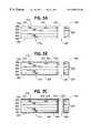
- FIG. 1illustrates the waveform of a modulated reverse electric current used for metallizing the HDI areas of a circuit board in the first step of the method of the invention.
- FIG. 2illustrates the waveform of a modulated reverse electric current used in metallizing the printed wiring board areas of a circuit board in the second step of the method of the invention.
- FIG. 3Aillustrates a cross section of a circuit board having both an HDI area and a PWB area before the first metallization step of the process of the invention.
- FIG. 3Billustrates a cross section of a circuit board having both an HDI area and a PWB area after the first metallization step of the process of the invention.
- FIG. 3Cillustrates a cross section of a circuit board having both an HDI area and a PWB area after the second metallization step of the process of the invention.
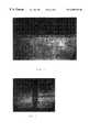
- FIG. 4is a photomicrograph of a cross section of a brass substrate having vias with a transverse dimension of about 75-100 micrometers after a first plating step according to the process of the invention.
- FIG. 5is a photomicrograph of a cross-section of the brass substrate having a through-hole with a diameter of about 325 micrometers at one end of the hole after the substrate has been treated with both steps of the process of the invention.
- FIG. 6is a photomicrograph of a cross-section of the brass substrate having a through-hole with a diameter of about 325 micrometers at the other end of the hole after the substrate has been treated with both steps of the process of the invention.
- the method of the inventionmakes use of the ability to control the deposition of metal into small recesses can be controlled by using a modulated reverse electric field that produces a pulsed reversing current.
- a cathodic pulseis applied to the substrate to produce reduction of metal ions and deposition of metal on the substrate.
- a following anodic pulsemay produce oxidation reactions at the substrate, e.g., oxidation of hydrogen produced by the preceding cathodic pulse, and may cause some dissolution of the metal deposited during the cathodic pulse.
- the cathodic and anodic pulsesmay effect the adsorption and desorption phenomena of the various components of the plating bath such as additives and the like.
- the duration, frequency and duty cycle of the anodic and cathodic pulsesit is possible to produce a net deposition of metal at selected locations on the substrate.
- the preferential electrodeposition of a metal into relatively small recessesis related to the relative dimensions of the recess and the Nernst diffusion layer, which develops in the electrolyte close to the surface of the substrate. Because the concentration of metal ions in the electrolyte contacting the substrate is depleted by deposition onto the substrate, a concentration gradient develops in the layer of electrolyte adjacent to the substrate surface. In this layer (the Nernst diffusion layer), having a thickness ⁇ , mass transport of metal ions from the bulk electrolyte to the surface takes place by diffusion. The thickness of the Nernst diffusion layer is determined by the vigor of the hydrodynamic agitation of the plating bath, and accordingly its thickness is subject to considerable variation.
- the thickness ⁇ of the Nernst diffusion layerhas been determined to be about 75 micrometers.
- the Nernst diffusion layergenerally conforms to the profile of the substrate surface, it is evident that for small recesses, i.e., those having transverse dimensions of the order of the thickness of the diffusion layer, or more specifically two times the thickness of the diffusion layer, the layer cannot follow the surface profile. Consequently, these recesses, wherein the metal ions to be deposited must diffuse over distances that are greater than the hydrodynamically defined Nernst diffusion layer, may be said to hydrodynamically inaccessible to the bulk electrolyte. Conversely, those portions of the substrate profile, including larger recesses and holes, wherein the plated metal ions have to traverse only the thickness of the Nernst diffusion layer may be said to be hydrodynamically accessible to the bulk electrolyte.
- the boundary between hydrodynamically accessible and hydrodynamically inaccessible recess in a substrate surfacedepends somewhat on the degree of agitation of the electrolyte bath.
- recesses having a transverse dimension of the order of twice the thickness of the Nernst diffusion layer, or perhaps somewhat greatermay be considered to be hydrodynamically accessible to the bulk electrolyte. Consequently, small recesses having transverse dimensions less than about 200-250 micrometers, or perhaps 350 micrometers at the outside, are hydrodynamically isolated.
- those recesses having relatively large aspect ratioswill tend to be relatively hydrodynamically inaccessible, because the diffusion layer simply cannot follow the surface profile.
- recesses having transverse dimensions greater than about 200-250 micrometersmay be ordinarily considered to be hydrodynamically accessible to the bulk electrolyte.
- size limits separating the hydrodynamically inaccessible recesses from the hydrodynamically accessible onescannot be defined in absolute dimensions, in a given case the dimensional boundary between the hydrodynamically accessible recesses and those that are hydrodynamically inaccessible can be determined, at least by the results of electroplating experiments.
- a pulsed reversing currenthaving a relatively short cathodic duty cycle, e.g., less than about 50%, and a relatively long anodic duty cycle, i.e., greater than about 50%.
- the hydrodynamically accessible recesses and holesare plated with a uniform layer of deposited metal using a pulsed reversing current having a relatively long cathodic duty cycle, i.e., greater than about 50%, and a relatively short anodic duty cycle, i.e., less than about 50%.
- a layer of metale.g., copper is deposited selectively in the small blind vias of a circuit board having an area of high density interconnections.
- the procedureis disclosed in copending U.S. patent application Ser. No. 09/231,811 the entire disclosure of which is incorporated herein by reference.
- the small features plated in the first step of the process of the inventiontypically have transverse dimensions less than about 350 micrometers, typically between about 5 micrometers and 350 micrometers, and more typically from about 10 micrometers to about 250 micrometers, or from about 25 micrometers to about 250 micrometers, and still more typically from about 50 micrometers to about 150 micrometers.
- FIG. 1A schematic representation of a rectangular modulated reverse electric field waveform used in the first step of the process of the invention is illustrated in FIG. 1 .
- the waveformessentially comprises a cathodic (forward) pulse followed by an anodic (reverse) pulse.
- An off-period or relaxation periodmay follow either or both of the cathodic and anodic pulses.
- the ordinate in FIG. 1could represent either current or voltage. Although it is generally more convenient in practice to control the current, alternatively the voltage may be controlled.
- the technical disclosure of the processis more straightforward if discussed in terms of the current flow.
- the waveformneed not be rectangular as illustrated.
- the cathodic and anodic pulsesmay have any voltage-time (or current-time) profile.
- rectangular pulsesare assumed for simplicity.
- the point in time chosen as the initial point of the pulse trainis entirely arbitrary.
- Either the cathodic pulse or the anodic pulse (or any point in the pulse train)could be considered as the initial point.
- the representation with the cathodic initial pulseis introduced for simplicity in discussion.
- the cathodic peak currentis shown as i 1 and the cathodic on-time is t 1 .
- the anodic peak currentis shown as i 2 and the anodic on-time is t 2 .
- the relaxation time, or off-timesare indicated by t a , and t b .
- the ratio of the cathodic on-time to the period (t 1 /T)is the cathodic duty cycle (D 1 ), and the ratio of the anodic on-time to the period (t 2 /T) is the anodic duty cycle (D 2 ).
- the current density, i.e., current per unit area of the electrode, during the cathodic on-time and anodic on-timeis known as the cathodic peak pulse current density and anodic peak pulse current density, respectively.
- the cathodic charge transfer density (Q 1 )is the product of the cathodic current density and the cathodic on-time (i 1 T 1 ), while the anodic charge transfer density (Q 2 ) is the product of the anodic current density and the anodic on-time (i 2 T 2 ).
- the average current density (I ave )is the average cathodic current density (D 1 I 1 ) density (D 1 I 1 ) minus the average anodic current density (I 2 D 2 ). Accordingly the relationships among the parameters may be represented by the following equations.
- the cathodic duty cycle in the first step of the process of the inventionshould be relatively short, less than about 50%, and the cathodic pulses should be relatively short, to favor uniform deposition of metal on both the concave (trenches) and convex (peaks) portions of the substrate surface as well as flat portions of the surface.
- the cathodic duty cycleis from about 30% to about 1%, more preferably from about 30% to about 15% and still more preferably from about 30% to about 20%.
- the anodic duty cycleshould be relatively long, greater than about 50%, and the anodic pulses should be relatively long in order to favor removal of excess metal from the convex and peak portions of the substrate surface and the flat portions of the surface.
- the anodic duty cycleis from about 60% to about 99%, more preferably from about 70% to about 85% and still more preferably from about 70% to about 80%. Because the anodic duty cycle is longer than the cathodic duty cycle, the peak anodic voltage (and corresponding current) will be less than the peak cathodic voltage (and corresponding current). Accordingly, the cathodic-to-anodic net charge ratio will be greater than one, in order to provide a net deposition of metal on the surface. Although the anodic removal of excess metal reduces the overall efficiency of the electroplating process, the benefits of filling or uniformly coating the trenches or blind vias required for high density interconnects provide great advantages in the manufacturing process.
- the frequency of the pulse train used in the method of the inventionmay range from about 10 Hertz to about 12000 Hertz, preferably from about 100 Hz to about 10000 Hz, more preferably from about 500 Hz to about 10000 Hz, and still more preferably from about 2000 Hz to about 10000 Hz. More specifically, the frequency of the pulse train used in the first electroplating step of the invention may range from about 10 Hertz to about 12000 Hertz, preferably from about 100 Hertz to about 6000 Hertz, and more preferably from about 500 Hertz to about 4000 Hertz. The frequency of the pulse train used in the second electroplating step of the invention may range from about 10 Hertz to about 5000 Hertz.
- the cathodic and anodic pulse widthsmay vary from about 1.0 microsecond to about 100 milliseconds. Generally, as the feature size decreases or the aspect ratio increases, higher frequencies and or lower cathodic duty cycles are preferred.
- An anodic pulseis introduced between at least some of the cathodic pulses. However, it is not excluded that two or more cathodic pulses may be introduced between a pair of anodic pulses. In particular, a plurality of very short cathodic pulses may be followed by one relatively long anodic pulse. Accordingly, a number of cathodic and anodic pulses with defined pulse widths may make up one group of pulses, which is then repeated.
- Such a groupwould include one or more cathodic pulses and at least one anodic pulse.
- the period of a pulse train comprised of such pulse groupsmay conveniently be defined as the time from the beginning of one cathodic pulse to the beginning of the next cathodic pulse that is similarly situated in the pulse train.
- the frequency of the pulse trainmay then be defined as the reciprocal of the period, as discussed above.
- the pulse width, duty cycle, and applied voltage of the cathodic and anodic pulsesmust be adjusted, within the parameters defined for the first step of the process, to provide that the overall process is cathodic, i.e., there is a net deposition of metal on the substrate workpiece.
- the practitionerwill adapt the pulse width, duty cycle, and frequency to a particular application, based on the principles and teachings of the process of the invention.
- metalis deposited uniformly over the relatively large features of the substrate and in the through holes that are typically found in circuit board substrates.
- the waveform of the pulsed reversing currentis selected to produce this uniform deposit over the relatively large features.
- FIG. 2A schematic representation of a rectangular modulated reverse electric field waveform used in the second step of the process of the invention is illustrated in FIG. 2 .
- the definitions of the relevant parameters of the pulse trainhave been set forth above.
- the cathodic pulseis relatively long and the anodic pulse is relatively short.
- the relatively long cathodic pulseswill deposit metal uniformly over the large features. Such pulses tend to deposit an excess of metal at the corners and peak portions of the substrate. They also tend to deposit excess metal at the corners of the through holes, yielding a so-called “dog-bone” profile.
- the relatively short anodic pulses in the second step of the inventiontend to remove metal from the corners and peaks of the substrate, thereby compensating for the overplating produced by the cathodic pulses.
- the resultis a smooth uniform coating of metal over the relatively large features of the substrate.
- the waveform used in the second step of the plating process of the inventionwill deposit a uniform coating of metal over features having transverse dimensions of about 350 micrometers or greater, or under come circumstances having features greater than about 250 micrometers. Such dimensions are typical of the through-holes of conventional circuit boards and of the holes placed in the peripheral connecting portions of high density interconnect circuit boards.
- the cathodic duty cycle in the second step of the process of the inventionis relatively long, more than about 50%, and the anodic pulses should be relatively short, less than that of the cathodic pulse and preferably less than about 50%.
- the cathodic duty cycleis from about 60% to about 99%, more preferably from about 70% to about 85% and still more preferably from about 70% to about 80%.
- the anodic duty cycleshould be relatively short, less than about 50%, and the anodic pulses should be relatively short in order to favor removal of excess metal from the convex and peak portions of the substrate surface.
- the anodic duty cycleis from about 30% to about 1%, more preferably from about 30% to about 15% and still more preferably from about 30% to about 20%.
- the peak anodic voltage (and corresponding current)may be greater than the peak cathodic voltage (and corresponding current).
- the cathodic-to-anodic net charge ratiois adjusted to be greater than one, in order to provide a net deposition of metal on the surface.
- the method of the inventionmay be used with any metal that can be deposited by electroplating techniques.
- copper, silver, gold, zinc, chromium, nickel, tin, lead and alloys thereofsuch as bronze, brass, solder, and the like, may be deposited by the process of the invention.
- FIGS. 3A-3CThe deposition of a metal on a circuit board having both small vias and large through-holes is illustrated in FIGS. 3A-3C.
- FIG. 3Aillustrates a cross section of a multi-layer circuit board 300 having features of different sizes to be plated with metal by the process of the invention.
- the surfaces 302 of the board 300are to be plated with an electrically conductive metal, e.g., copper, which can be subsequently masked and etched to provide conductive traces on the surfaces 302 of the board 300 .
- the illustrated boardhas five layers of dielectric material 304 , 306 , although it will be understood by those skilled in the art that boards having any conventional number of layers can be used.
- the inner dielectric layers 304will be a reinforced material such as glass fiber reinforced epoxy resin.
- the outer layers 306may be an unreinforced material, e.g., unreinforced epoxy resin, to permit easier drilling of vias.
- the board 300may contain a number of conducting paths formed at the interfaces between the layers 304 , 306 . These conductors are shown in cross-section as conductors fully buried conductors 308 and conductors 310 to be connected to the surface 302 of the board 300 . Vias 312 , 314 are formed in the outer dielectric layers 306 to provide for connecting the conductors 310 to pattern of conductive traces on the surface of the finished circuit board.
- the circuit board 300may contain through-holes, one of which is shown as 320 , which are intended to be metallized to connect the conductors on the surface 302 to buried pads 328 .
- the surfaces to be platede.g., the surfaces 302 , the interior surfaces of the vias 312 , 314 and the inside of the through-hole 320 are covered with a thin layer of a conductor by conventional procedures, e.g., by sputtering, electroless deposition, or the like.
- Circuit board 300is then immersed in a plating bath containing ions of a metal to be deposited, e.g., copper ions.
- the plating bathmay be any conventional plating bath appropriate for the metal being plated.
- plating baths for depositing coppercontain a copper salt, e.g., copper sulfate, sulfuric acid, a carrier material that is typically a polyethylene glycol, chloride ion, and one or more proprietary additives generally known as brighteners, levelers, and the like, to improve the uniformity, surface finish, and strength of the deposited coating.
- the process of the inventioncan be carried out using conventional copper plating baths, it has been found that satisfactory copper deposits can be achieved using a bath that does not include the conventional brighteners, levelers, and the like. Accordingly, for electroplating copper onto an HDI substrate, particularly when small traces and vias are to be prepared, it is preferred to avoid conventional additives such as leveling agents and the like, in order to avoid the difficulties of using such additives such as the tight control of concentration of said additives as well as possible inclusion in the plated conductors.
- a preferred bath for electroplating copper according to the process of the inventionis an aqueous acidic copper sulfate bath incorporating about 40 to about 80 g/L of copper sulfate, a molar ratio of sulfuric acid to copper sulfate of about 5:1 to about 8:1, about 5% of polyethylene glycol and about 30 ppm to about 60 ppm of chloride ion.
- An electric currentis then passed between the circuit board and a counterelectrode immersed in the plating bath by imposing a modulated reversing electric field to deposit the metal, e.g., copper, on the surfaces of the board 300 .
- the currentis a pulsed reversing current as discussed above, having relatively short cathodic pulses, i.e., having a duty cycle less than about 50%, and long anodic pulses, i.e., having a duty cycle greater than about 50%.
- a pulsed reversing currentwill produce a layer of plated copper 324 that will provide a conductive path between the vias on the surface 302 of the board 300 .
- the deposit in the first stepcan provide a conformal coating in the vias as shown at 314 or may completely fill the vias, as shown at 312 . Both types of coating in the vias are shown for illustrative purposes, although in general only one type will be deposited in a given application of the process.
- the pulsed reversing current having the waveform used in the first step of the processwill typically deposit a relatively thin layer of conductive metal over the surface 302 of the board 300 , and will deposit little or no metal on the inner surface 322 of the through-hole 320 . Accordingly, after the vias have been metallized, a second plating step is performed using a waveform that will deposit a uniform layer of conductive metal over the surfaces 302 of the board 300 and also on the interior surface 322 of the through hole 320 .
- the pulsed reversing current used in the second step of the process of the inventioncomprises cathodic pulses having a relatively long duty cycle, typically greater than about 50% and the anodic pulses have a duty cycle typically greater than about 50%.
- the cathodic pulses in the second step of the processhave a duty cycle of about 60% to about 99%, more preferably from about 70% to about 95% and still more preferably from about 85% to about 95%.
- the anodic pulses in the second step of the processpreferably have a duty cycle of from about 1% to about 40%, more preferably from about 5% to about 30% and more preferably from about 5% to about 15%.
- FIG. 3Cshows a schematic cross section of the circuit board 300 after the second step of the process.
- a uniform layer 326 of copperhas been deposited over the first layer 324 and onto the inner surface 322 of the through-hole 320 .
- the uniformly plated board 300can then be masked, imaged and etched by conventional procedures to provide conductive traces on the surfaces 302 of the board 300 .
- This exampleillustrates the preparation of a substrate having filled vias and a uniform surface deposit of copper by the process of the invention.
- small blind holes having a diameter of about 75-100 micrometerswere drilled in the surface of a brass panel having dimensions of 18 inches ⁇ 8 inches using a laser. Through holes having a diameter of about 325 micrometers were also made in the plate using a mechanical drill.
- the platewas mounted in a conventional industrial circuit board electroplating apparatus and plated in two steps according to the invention.
- the plating bathhad the following composition: 60-65 g/L of copper sulfate, 166 g/L of sulfuric acid, about 50 parts per million (ppm) of chloride ion, and about 300 ppm of polyethylene glycol (PEG).
- cathodic duty cycle33%; anodic duty cycle, 67%; average cathodic current density, 25 amperes per square foot (ASF), frequency of pulse train, about 333 Hz, and cathodic/anodic charge ratio (Q c /Q a ) , 2.5.
- the platingwas conducted for a period of 3 hours in the first step.
- the second step of the plating processwas then conducted by merely changing the waveform of the plating current.
- the bathwas not changed, the board was not removed from the plating apparatus and no other processing steps were conducted.
- the pulsed reversing electric currenthad the following characteristics: cathodic duty cycle, 90%; anodic duty cycle, 10%; average cathodic current density, 25 amperes per square foot (ASF), frequency of pulse train, about 100 Hz, and cathodic/anodic charge ratio (Q c /Q a ) 10.
- the platingwas conducted for a period of 1 hour in the second step.
- FIG. 4is a photomicrograph of a cross-section of the plated substrate showing the vias filled with deposited copper. (Certain defects in the brass test panel are also visible.)
- FIGS. 5 and 6are photomicrographs showing cross sections of the substrate at each end of the through hole showing a generally uniform plating of the surface of the substrate and the interior surface of the through-hole, with minimum excessive plating (“dogboning”) at the edge of the hole.
Landscapes
- Chemical & Material Sciences (AREA)
- Engineering & Computer Science (AREA)
- Chemical Kinetics & Catalysis (AREA)
- Electrochemistry (AREA)
- Materials Engineering (AREA)
- Metallurgy (AREA)
- Organic Chemistry (AREA)
- Manufacturing & Machinery (AREA)
- Microelectronics & Electronic Packaging (AREA)
- Electroplating Methods And Accessories (AREA)
Abstract
Description

Claims (23)
Priority Applications (5)
| Application Number | Priority Date | Filing Date | Title |
|---|---|---|---|
| US09/419,881US6309528B1 (en) | 1999-10-15 | 1999-10-18 | Sequential electrodeposition of metals using modulated electric fields for manufacture of circuit boards having features of different sizes |
| PCT/US2000/028313WO2001029878A2 (en) | 1999-10-15 | 2000-10-13 | Sequential electrodeposition of metals using modulated electric fields for manufacture of circuit boards having features of different sizes |
| AU10828/01AAU1082801A (en) | 1999-10-15 | 2000-10-13 | Sequential electrodeposition of metals using modulated electric fields for manufacture of circuit boards having features of different sizes |
| US09/823,750US6863793B2 (en) | 1999-10-15 | 2001-04-03 | Sequential electrodeposition of metals using modulated electric fields for manufacture of circuit boards having features of different sizes |
| US10/132,399US6652727B2 (en) | 1999-10-15 | 2002-04-26 | Sequential electrodeposition of metals using modulated electric fields for manufacture of circuit boards having features of different sizes |
Applications Claiming Priority (2)
| Application Number | Priority Date | Filing Date | Title |
|---|---|---|---|
| US15954199P | 1999-10-15 | 1999-10-15 | |
| US09/419,881US6309528B1 (en) | 1999-10-15 | 1999-10-18 | Sequential electrodeposition of metals using modulated electric fields for manufacture of circuit boards having features of different sizes |
Related Child Applications (1)
| Application Number | Title | Priority Date | Filing Date |
|---|---|---|---|
| US09/823,750Continuation-In-PartUS6863793B2 (en) | 1999-10-15 | 2001-04-03 | Sequential electrodeposition of metals using modulated electric fields for manufacture of circuit boards having features of different sizes |
Publications (1)
| Publication Number | Publication Date |
|---|---|
| US6309528B1true US6309528B1 (en) | 2001-10-30 |
Family
ID=26856055
Family Applications (2)
| Application Number | Title | Priority Date | Filing Date |
|---|---|---|---|
| US09/419,881Expired - LifetimeUS6309528B1 (en) | 1999-10-15 | 1999-10-18 | Sequential electrodeposition of metals using modulated electric fields for manufacture of circuit boards having features of different sizes |
| US09/823,750Expired - Fee RelatedUS6863793B2 (en) | 1999-10-15 | 2001-04-03 | Sequential electrodeposition of metals using modulated electric fields for manufacture of circuit boards having features of different sizes |
Family Applications After (1)
| Application Number | Title | Priority Date | Filing Date |
|---|---|---|---|
| US09/823,750Expired - Fee RelatedUS6863793B2 (en) | 1999-10-15 | 2001-04-03 | Sequential electrodeposition of metals using modulated electric fields for manufacture of circuit boards having features of different sizes |
Country Status (3)
| Country | Link |
|---|---|
| US (2) | US6309528B1 (en) |
| AU (1) | AU1082801A (en) |
| WO (1) | WO2001029878A2 (en) |
Cited By (49)
| Publication number | Priority date | Publication date | Assignee | Title |
|---|---|---|---|---|
| US6528424B1 (en)* | 2002-02-22 | 2003-03-04 | Advanced Micro Devices, Inc. | Method of electroplating a copper-zinc alloy thin film on a copper surface using a chemical solution |
| WO2003033776A1 (en)* | 2001-10-15 | 2003-04-24 | Faraday Technology, Inc. | Electrodeposition of metals in high-aspect ratio cavities using modulated reverse electric fields. |
| EP1323850A1 (en)* | 2001-12-18 | 2003-07-02 | Shipley Co. L.L.C. | Electroplating method of printed circuit with pulsed current density |
| US20030201185A1 (en)* | 2002-04-29 | 2003-10-30 | Applied Materials, Inc. | In-situ pre-clean for electroplating process |
| US6652727B2 (en)* | 1999-10-15 | 2003-11-25 | Faraday Technology Marketing Group, Llc | Sequential electrodeposition of metals using modulated electric fields for manufacture of circuit boards having features of different sizes |
| US20030221967A1 (en)* | 2002-01-15 | 2003-12-04 | Shipley Company, L.L.C. | Via filling method |
| US20040004006A1 (en)* | 2002-06-12 | 2004-01-08 | Taylor E. Jennings | Electrolytic etching of metal layers |
| US20040072423A1 (en)* | 2001-01-12 | 2004-04-15 | Jacob Jorne | Methods and systems for electro-or electroless-plating of metal in high-aspect ratio features |
| US20040118691A1 (en)* | 2002-12-23 | 2004-06-24 | Shipley Company, L.L.C. | Electroplating method |
| US20040188260A1 (en)* | 2003-03-31 | 2004-09-30 | Matthias Bonkabeta | Method of plating a semiconductor structure |
| US20040226745A1 (en)* | 1999-08-06 | 2004-11-18 | Ibiden Co., Ltd. | Electroplating solution, method for manufacturing multilayer printed circuit board using the same solution, and multilayer printed circuit board |
| US20040262165A1 (en)* | 2003-04-16 | 2004-12-30 | Hiroyuki Kanda | Plating method |
| US20050145506A1 (en)* | 2003-12-29 | 2005-07-07 | Taylor E. J. | Electrochemical etching of circuitry for high density interconnect electronic modules |
| US20050178668A1 (en)* | 2003-11-21 | 2005-08-18 | Andreas Mobius | Method for depositing nickel- and chromium (VI) -free metal matte layers |
| US20050205429A1 (en)* | 2004-03-19 | 2005-09-22 | Gebhart Lawrence E | Electroplating cell with hydrodynamics facilitating more uniform deposition across a workpiece during plating |
| US20060207888A1 (en)* | 2003-12-29 | 2006-09-21 | Taylor E J | Electrochemical etching of circuitry for high density interconnect electronic modules |
| US20070257208A1 (en)* | 2006-05-05 | 2007-11-08 | Virgin Islands Microsystems, Inc. | Electron accelerator for ultra-small resonant structures |
| US20080035475A1 (en)* | 2004-03-19 | 2008-02-14 | Faraday Technology, Inc. | Electroplating cell with hydrodynamics facilitating more uniform deposition on a workpiece with through holes during plating |
| US20080041728A1 (en)* | 2006-08-09 | 2008-02-21 | Paul Chalmer | Electrolytic looping for forming layering in the deposit of a coating |
| US20080217180A1 (en)* | 2004-08-26 | 2008-09-11 | Siemens Aktiengesellschaft | Surface with an Anti-Adhesion Microstructure and Method for Producing Same |
| US7579609B2 (en) | 2005-12-14 | 2009-08-25 | Virgin Islands Microsystems, Inc. | Coupling light of light emitting resonator to waveguide |
| US20090230332A1 (en)* | 2007-10-10 | 2009-09-17 | Virgin Islands Microsystems, Inc. | Depressed Anode With Plasmon-Enabled Devices Such As Ultra-Small Resonant Structures |
| US7626179B2 (en) | 2005-09-30 | 2009-12-01 | Virgin Island Microsystems, Inc. | Electron beam induced resonance |
| US7646991B2 (en) | 2006-04-26 | 2010-01-12 | Virgin Island Microsystems, Inc. | Selectable frequency EMR emitter |
| US7655934B2 (en) | 2006-06-28 | 2010-02-02 | Virgin Island Microsystems, Inc. | Data on light bulb |
| US7679067B2 (en) | 2006-05-26 | 2010-03-16 | Virgin Island Microsystems, Inc. | Receiver array using shared electron beam |
| US7688274B2 (en) | 2006-02-28 | 2010-03-30 | Virgin Islands Microsystems, Inc. | Integrated filter in antenna-based detector |
| US7710040B2 (en) | 2006-05-05 | 2010-05-04 | Virgin Islands Microsystems, Inc. | Single layer construction for ultra small devices |
| US7718977B2 (en) | 2006-05-05 | 2010-05-18 | Virgin Island Microsystems, Inc. | Stray charged particle removal device |
| US7723698B2 (en) | 2006-05-05 | 2010-05-25 | Virgin Islands Microsystems, Inc. | Top metal layer shield for ultra-small resonant structures |
| US7728702B2 (en) | 2006-05-05 | 2010-06-01 | Virgin Islands Microsystems, Inc. | Shielding of integrated circuit package with high-permeability magnetic material |
| US7728397B2 (en) | 2006-05-05 | 2010-06-01 | Virgin Islands Microsystems, Inc. | Coupled nano-resonating energy emitting structures |
| US7732786B2 (en) | 2006-05-05 | 2010-06-08 | Virgin Islands Microsystems, Inc. | Coupling energy in a plasmon wave to an electron beam |
| US7741934B2 (en) | 2006-05-05 | 2010-06-22 | Virgin Islands Microsystems, Inc. | Coupling a signal through a window |
| US7746532B2 (en) | 2006-05-05 | 2010-06-29 | Virgin Island Microsystems, Inc. | Electro-optical switching system and method |
| US7791290B2 (en) | 2005-09-30 | 2010-09-07 | Virgin Islands Microsystems, Inc. | Ultra-small resonating charged particle beam modulator |
| US20100300888A1 (en)* | 2009-05-27 | 2010-12-02 | Ponnuswamy Thomas A | Pulse sequence for plating on thin seed layers |
| US7876793B2 (en) | 2006-04-26 | 2011-01-25 | Virgin Islands Microsystems, Inc. | Micro free electron laser (FEL) |
| US7986113B2 (en) | 2006-05-05 | 2011-07-26 | Virgin Islands Microsystems, Inc. | Selectable frequency light emitter |
| US7990336B2 (en) | 2007-06-19 | 2011-08-02 | Virgin Islands Microsystems, Inc. | Microwave coupled excitation of solid state resonant arrays |
| US8123927B1 (en)* | 2003-09-23 | 2012-02-28 | Rockstar Bidco, LP | Reduced circuit trace roughness for improved signal performance |
| US8188431B2 (en) | 2006-05-05 | 2012-05-29 | Jonathan Gorrell | Integration of vacuum microelectronic device with integrated circuit |
| US8384042B2 (en) | 2006-01-05 | 2013-02-26 | Advanced Plasmonics, Inc. | Switching micro-resonant structures by modulating a beam of charged particles |
| US20140238864A1 (en)* | 2013-02-27 | 2014-08-28 | Taiwan Semiconductor Manufacturing Co. Ltd. | Layer by Layer Electro Chemical Plating (ECP) Process |
| US9385035B2 (en) | 2010-05-24 | 2016-07-05 | Novellus Systems, Inc. | Current ramping and current pulsing entry of substrates for electroplating |
| US10684522B2 (en) | 2017-12-07 | 2020-06-16 | Faraday Technology, Inc. | Electrochemical mirror system and method |
| US11411258B2 (en) | 2018-09-05 | 2022-08-09 | Faraday Technology, Inc. | Pulse reverse current high rate electrodeposition and charging while mitigating the adverse effects of dendrite formation |
| CN119640351A (en)* | 2024-12-02 | 2025-03-18 | 广东工业大学 | Glass adapter plate, filling method of glass through holes of glass adapter plate and chip |
| US12305307B2 (en) | 2020-01-10 | 2025-05-20 | Lam Research Corporation | TSV process window and fill performance enhancement by long pulsing and ramping |
Families Citing this family (11)
| Publication number | Priority date | Publication date | Assignee | Title |
|---|---|---|---|---|
| JP4000796B2 (en)* | 2001-08-08 | 2007-10-31 | 株式会社豊田自動織機 | Via hole copper plating method |
| EP1475463B2 (en)† | 2002-12-20 | 2017-03-01 | Shipley Company, L.L.C. | Reverse pulse plating method |
| JP2005191148A (en)* | 2003-12-24 | 2005-07-14 | Sanyo Electric Co Ltd | Hybrid integrated circuit device and manufacturing method thereof |
| US20060037861A1 (en)* | 2004-08-23 | 2006-02-23 | Manos Paul D | Electrodeposition process |
| US7425255B2 (en)* | 2005-06-07 | 2008-09-16 | Massachusetts Institute Of Technology | Method for producing alloy deposits and controlling the nanostructure thereof using negative current pulsing electro-deposition |
| WO2007082112A2 (en)* | 2006-01-06 | 2007-07-19 | Faraday Technology, Inc. | Tin and tin alloy electroplating method with controlled internal stress and grain size of the resulting deposit |
| CN103603018B (en)* | 2013-10-23 | 2016-05-11 | 复旦大学 | A kind of pulse plating method and application thereof |
| US9758893B2 (en) | 2014-02-07 | 2017-09-12 | Applied Materials, Inc. | Electroplating methods for semiconductor substrates |
| CN105316716A (en)* | 2015-11-30 | 2016-02-10 | 苏州市金星工艺镀饰有限公司 | Electroplating liquid for pulse electroplating for compact silver film on ceramic surface and electroplating method thereof |
| US10920334B2 (en) | 2016-03-22 | 2021-02-16 | The Trustees Of Princeton University | Electrohydrodynamically formed structures of carbonaceous material |
| CN112030203B (en)* | 2020-08-28 | 2021-10-26 | 生益电子股份有限公司 | Through hole electroplating filling method and preparation method of printed circuit board |
Citations (7)
| Publication number | Priority date | Publication date | Assignee | Title |
|---|---|---|---|---|
| US3802854A (en)* | 1973-03-19 | 1974-04-09 | Akad Wissenschaften Ddr | Process for forming magnetic metal deposits on a flexible base for use as information data carrier product thereof |
| US4396467A (en)* | 1980-10-27 | 1983-08-02 | General Electric Company | Periodic reverse current pulsing to form uniformly sized feed through conductors |
| US4519877A (en)* | 1982-12-06 | 1985-05-28 | Fine Particle Technology Corporation | Formation of narrow conductive paths on a substrate |
| US4666567A (en)* | 1981-07-31 | 1987-05-19 | The Boeing Company | Automated alternating polarity pulse electrolytic processing of electrically conductive substances |
| US5863406A (en)* | 1995-07-06 | 1999-01-26 | International Business Machines Corp. | Method of manufacturing a printed circuit board |
| US5972192A (en)* | 1997-07-23 | 1999-10-26 | Advanced Micro Devices, Inc. | Pulse electroplating copper or copper alloys |
| US5980721A (en)* | 1997-02-11 | 1999-11-09 | Thomson-Csf | Fabrication method for double metallic resist printed circuit boards |
Family Cites Families (1)
| Publication number | Priority date | Publication date | Assignee | Title |
|---|---|---|---|---|
| US4140596A (en)* | 1975-12-22 | 1979-02-20 | Vereinigte Metallwerke Ranshofen-Berndorf Aktiengesellschaft | Process for the electrolytic refining of copper |
- 1999
- 1999-10-18USUS09/419,881patent/US6309528B1/ennot_activeExpired - Lifetime
- 2000
- 2000-10-13WOPCT/US2000/028313patent/WO2001029878A2/enactiveApplication Filing
- 2000-10-13AUAU10828/01Apatent/AU1082801A/ennot_activeAbandoned
- 2001
- 2001-04-03USUS09/823,750patent/US6863793B2/ennot_activeExpired - Fee Related
Patent Citations (7)
| Publication number | Priority date | Publication date | Assignee | Title |
|---|---|---|---|---|
| US3802854A (en)* | 1973-03-19 | 1974-04-09 | Akad Wissenschaften Ddr | Process for forming magnetic metal deposits on a flexible base for use as information data carrier product thereof |
| US4396467A (en)* | 1980-10-27 | 1983-08-02 | General Electric Company | Periodic reverse current pulsing to form uniformly sized feed through conductors |
| US4666567A (en)* | 1981-07-31 | 1987-05-19 | The Boeing Company | Automated alternating polarity pulse electrolytic processing of electrically conductive substances |
| US4519877A (en)* | 1982-12-06 | 1985-05-28 | Fine Particle Technology Corporation | Formation of narrow conductive paths on a substrate |
| US5863406A (en)* | 1995-07-06 | 1999-01-26 | International Business Machines Corp. | Method of manufacturing a printed circuit board |
| US5980721A (en)* | 1997-02-11 | 1999-11-09 | Thomson-Csf | Fabrication method for double metallic resist printed circuit boards |
| US5972192A (en)* | 1997-07-23 | 1999-10-26 | Advanced Micro Devices, Inc. | Pulse electroplating copper or copper alloys |
Cited By (72)
| Publication number | Priority date | Publication date | Assignee | Title |
|---|---|---|---|---|
| US20050211561A1 (en)* | 1999-08-06 | 2005-09-29 | Ibiden Co., Ltd. | Electroplating solution, method for manufacturing multilayer printed circuit board using the same solution, and multilayer printed circuit board |
| US7446263B2 (en)* | 1999-08-06 | 2008-11-04 | Ibiden Co., Ltd. | Multilayer printed circuit board |
| US20040226745A1 (en)* | 1999-08-06 | 2004-11-18 | Ibiden Co., Ltd. | Electroplating solution, method for manufacturing multilayer printed circuit board using the same solution, and multilayer printed circuit board |
| US7993510B2 (en) | 1999-08-06 | 2011-08-09 | Ibiden Co., Ltd. | Electroplating solution, method for manufacturing multilayer printed circuit board using the same solution, and multilayer printed circuit board |
| US7812262B2 (en) | 1999-08-06 | 2010-10-12 | Ibiden Co., Ltd. | Multilayer printed circuit board |
| US7514637B1 (en) | 1999-08-06 | 2009-04-07 | Ibiden Co., Ltd. | Electroplating solution, method for fabricating multilayer printed wiring board using the solution, and multilayer printed wiring board |
| US6652727B2 (en)* | 1999-10-15 | 2003-11-25 | Faraday Technology Marketing Group, Llc | Sequential electrodeposition of metals using modulated electric fields for manufacture of circuit boards having features of different sizes |
| US20040072423A1 (en)* | 2001-01-12 | 2004-04-15 | Jacob Jorne | Methods and systems for electro-or electroless-plating of metal in high-aspect ratio features |
| WO2003033776A1 (en)* | 2001-10-15 | 2003-04-24 | Faraday Technology, Inc. | Electrodeposition of metals in high-aspect ratio cavities using modulated reverse electric fields. |
| US6827833B2 (en)* | 2001-10-15 | 2004-12-07 | Faraday Technology Marketing Group, Llc | Electrodeposition of metals in high-aspect ratio cavities using modulated reverse electric fields |
| EP1323850A1 (en)* | 2001-12-18 | 2003-07-02 | Shipley Co. L.L.C. | Electroplating method of printed circuit with pulsed current density |
| US20030221967A1 (en)* | 2002-01-15 | 2003-12-04 | Shipley Company, L.L.C. | Via filling method |
| EP1330146A3 (en)* | 2002-01-15 | 2004-04-07 | Shipley Co. L.L.C. | Via filling method |
| US6528424B1 (en)* | 2002-02-22 | 2003-03-04 | Advanced Micro Devices, Inc. | Method of electroplating a copper-zinc alloy thin film on a copper surface using a chemical solution |
| US20030201185A1 (en)* | 2002-04-29 | 2003-10-30 | Applied Materials, Inc. | In-situ pre-clean for electroplating process |
| US20040004006A1 (en)* | 2002-06-12 | 2004-01-08 | Taylor E. Jennings | Electrolytic etching of metal layers |
| US7022216B2 (en) | 2002-06-12 | 2006-04-04 | Faraday Technology Marketing Group, Llc | Electrolytic etching of metal layers |
| US20040011666A1 (en)* | 2002-06-12 | 2004-01-22 | Taylor E. Jennings | Electrolytic etching of metal layers |
| US20040118691A1 (en)* | 2002-12-23 | 2004-06-24 | Shipley Company, L.L.C. | Electroplating method |
| DE10314502B4 (en)* | 2003-03-31 | 2008-06-12 | Advanced Micro Devices, Inc., Sunnyvale | Process for the electrolytic coating of a semiconductor structure |
| US20040188260A1 (en)* | 2003-03-31 | 2004-09-30 | Matthias Bonkabeta | Method of plating a semiconductor structure |
| US20040262165A1 (en)* | 2003-04-16 | 2004-12-30 | Hiroyuki Kanda | Plating method |
| US8123927B1 (en)* | 2003-09-23 | 2012-02-28 | Rockstar Bidco, LP | Reduced circuit trace roughness for improved signal performance |
| US20050178668A1 (en)* | 2003-11-21 | 2005-08-18 | Andreas Mobius | Method for depositing nickel- and chromium (VI) -free metal matte layers |
| US20060207888A1 (en)* | 2003-12-29 | 2006-09-21 | Taylor E J | Electrochemical etching of circuitry for high density interconnect electronic modules |
| US20050145506A1 (en)* | 2003-12-29 | 2005-07-07 | Taylor E. J. | Electrochemical etching of circuitry for high density interconnect electronic modules |
| US8329006B2 (en) | 2004-03-19 | 2012-12-11 | Faraday Technology, Inc. | Electroplating cell with hydrodynamics facilitating more uniform deposition across a workpiece during plating |
| US20080035475A1 (en)* | 2004-03-19 | 2008-02-14 | Faraday Technology, Inc. | Electroplating cell with hydrodynamics facilitating more uniform deposition on a workpiece with through holes during plating |
| US7553401B2 (en) | 2004-03-19 | 2009-06-30 | Faraday Technology, Inc. | Electroplating cell with hydrodynamics facilitating more uniform deposition across a workpiece during plating |
| US20090205953A1 (en)* | 2004-03-19 | 2009-08-20 | Faraday Technology, Inc. | Electroplating cell with hydrodynamics facilitating more uniform deposition across a workpiece during plating |
| US8226804B2 (en) | 2004-03-19 | 2012-07-24 | The United States Of America As Represented By The Secretary Of The Air Force | Electroplating cell with hydrodynamics facilitating more uniform deposition on a workpiece with through holes during plating |
| US20050205429A1 (en)* | 2004-03-19 | 2005-09-22 | Gebhart Lawrence E | Electroplating cell with hydrodynamics facilitating more uniform deposition across a workpiece during plating |
| US7947161B2 (en) | 2004-03-19 | 2011-05-24 | Faraday Technology, Inc. | Method of operating an electroplating cell with hydrodynamics facilitating more uniform deposition on a workpiece with through holes |
| US20110209991A1 (en)* | 2004-03-19 | 2011-09-01 | Gebhart Lawrence E | Electroplating cell with hydrodynamics facilitating more uniform deposition on a workpiece with through holes during plating |
| US7758739B2 (en) | 2004-08-13 | 2010-07-20 | Virgin Islands Microsystems, Inc. | Methods of producing structures for electron beam induced resonance using plating and/or etching |
| US20080217180A1 (en)* | 2004-08-26 | 2008-09-11 | Siemens Aktiengesellschaft | Surface with an Anti-Adhesion Microstructure and Method for Producing Same |
| US7791291B2 (en) | 2005-09-30 | 2010-09-07 | Virgin Islands Microsystems, Inc. | Diamond field emission tip and a method of formation |
| US7791290B2 (en) | 2005-09-30 | 2010-09-07 | Virgin Islands Microsystems, Inc. | Ultra-small resonating charged particle beam modulator |
| US7626179B2 (en) | 2005-09-30 | 2009-12-01 | Virgin Island Microsystems, Inc. | Electron beam induced resonance |
| US7714513B2 (en) | 2005-09-30 | 2010-05-11 | Virgin Islands Microsystems, Inc. | Electron beam induced resonance |
| US7579609B2 (en) | 2005-12-14 | 2009-08-25 | Virgin Islands Microsystems, Inc. | Coupling light of light emitting resonator to waveguide |
| US8384042B2 (en) | 2006-01-05 | 2013-02-26 | Advanced Plasmonics, Inc. | Switching micro-resonant structures by modulating a beam of charged particles |
| US7688274B2 (en) | 2006-02-28 | 2010-03-30 | Virgin Islands Microsystems, Inc. | Integrated filter in antenna-based detector |
| US7876793B2 (en) | 2006-04-26 | 2011-01-25 | Virgin Islands Microsystems, Inc. | Micro free electron laser (FEL) |
| US7646991B2 (en) | 2006-04-26 | 2010-01-12 | Virgin Island Microsystems, Inc. | Selectable frequency EMR emitter |
| US7723698B2 (en) | 2006-05-05 | 2010-05-25 | Virgin Islands Microsystems, Inc. | Top metal layer shield for ultra-small resonant structures |
| US7746532B2 (en) | 2006-05-05 | 2010-06-29 | Virgin Island Microsystems, Inc. | Electro-optical switching system and method |
| US7728397B2 (en) | 2006-05-05 | 2010-06-01 | Virgin Islands Microsystems, Inc. | Coupled nano-resonating energy emitting structures |
| US20070257208A1 (en)* | 2006-05-05 | 2007-11-08 | Virgin Islands Microsystems, Inc. | Electron accelerator for ultra-small resonant structures |
| US7728702B2 (en) | 2006-05-05 | 2010-06-01 | Virgin Islands Microsystems, Inc. | Shielding of integrated circuit package with high-permeability magnetic material |
| US7732786B2 (en) | 2006-05-05 | 2010-06-08 | Virgin Islands Microsystems, Inc. | Coupling energy in a plasmon wave to an electron beam |
| US7718977B2 (en) | 2006-05-05 | 2010-05-18 | Virgin Island Microsystems, Inc. | Stray charged particle removal device |
| US8188431B2 (en) | 2006-05-05 | 2012-05-29 | Jonathan Gorrell | Integration of vacuum microelectronic device with integrated circuit |
| US7710040B2 (en) | 2006-05-05 | 2010-05-04 | Virgin Islands Microsystems, Inc. | Single layer construction for ultra small devices |
| US7986113B2 (en) | 2006-05-05 | 2011-07-26 | Virgin Islands Microsystems, Inc. | Selectable frequency light emitter |
| US7741934B2 (en) | 2006-05-05 | 2010-06-22 | Virgin Islands Microsystems, Inc. | Coupling a signal through a window |
| US7656094B2 (en) | 2006-05-05 | 2010-02-02 | Virgin Islands Microsystems, Inc. | Electron accelerator for ultra-small resonant structures |
| US7679067B2 (en) | 2006-05-26 | 2010-03-16 | Virgin Island Microsystems, Inc. | Receiver array using shared electron beam |
| US7655934B2 (en) | 2006-06-28 | 2010-02-02 | Virgin Island Microsystems, Inc. | Data on light bulb |
| US20080041728A1 (en)* | 2006-08-09 | 2008-02-21 | Paul Chalmer | Electrolytic looping for forming layering in the deposit of a coating |
| US7990336B2 (en) | 2007-06-19 | 2011-08-02 | Virgin Islands Microsystems, Inc. | Microwave coupled excitation of solid state resonant arrays |
| US20090230332A1 (en)* | 2007-10-10 | 2009-09-17 | Virgin Islands Microsystems, Inc. | Depressed Anode With Plasmon-Enabled Devices Such As Ultra-Small Resonant Structures |
| US7791053B2 (en) | 2007-10-10 | 2010-09-07 | Virgin Islands Microsystems, Inc. | Depressed anode with plasmon-enabled devices such as ultra-small resonant structures |
| US20100300888A1 (en)* | 2009-05-27 | 2010-12-02 | Ponnuswamy Thomas A | Pulse sequence for plating on thin seed layers |
| US8500983B2 (en)* | 2009-05-27 | 2013-08-06 | Novellus Systems, Inc. | Pulse sequence for plating on thin seed layers |
| US9385035B2 (en) | 2010-05-24 | 2016-07-05 | Novellus Systems, Inc. | Current ramping and current pulsing entry of substrates for electroplating |
| US20140238864A1 (en)* | 2013-02-27 | 2014-08-28 | Taiwan Semiconductor Manufacturing Co. Ltd. | Layer by Layer Electro Chemical Plating (ECP) Process |
| US9435048B2 (en)* | 2013-02-27 | 2016-09-06 | Taiwan Semiconductor Manufacturing Co., Ltd. | Layer by layer electro chemical plating (ECP) process |
| US10684522B2 (en) | 2017-12-07 | 2020-06-16 | Faraday Technology, Inc. | Electrochemical mirror system and method |
| US11411258B2 (en) | 2018-09-05 | 2022-08-09 | Faraday Technology, Inc. | Pulse reverse current high rate electrodeposition and charging while mitigating the adverse effects of dendrite formation |
| US12305307B2 (en) | 2020-01-10 | 2025-05-20 | Lam Research Corporation | TSV process window and fill performance enhancement by long pulsing and ramping |
| CN119640351A (en)* | 2024-12-02 | 2025-03-18 | 广东工业大学 | Glass adapter plate, filling method of glass through holes of glass adapter plate and chip |
Also Published As
| Publication number | Publication date |
|---|---|
| US6863793B2 (en) | 2005-03-08 |
| WO2001029878A3 (en) | 2001-12-06 |
| WO2001029878A9 (en) | 2002-08-01 |
| AU1082801A (en) | 2001-04-30 |
| WO2001029878A2 (en) | 2001-04-26 |
| US20020038764A1 (en) | 2002-04-04 |
Similar Documents
| Publication | Publication Date | Title |
|---|---|---|
| US6309528B1 (en) | Sequential electrodeposition of metals using modulated electric fields for manufacture of circuit boards having features of different sizes | |
| US6652727B2 (en) | Sequential electrodeposition of metals using modulated electric fields for manufacture of circuit boards having features of different sizes | |
| US6210555B1 (en) | Electrodeposition of metals in small recesses for manufacture of high density interconnects using reverse pulse plating | |
| AU765242B2 (en) | Electrodeposition of metals in small recesses using modulated electric fields | |
| US6524461B2 (en) | Electrodeposition of metals in small recesses using modulated electric fields | |
| US6750144B2 (en) | Method for electrochemical metallization and planarization of semiconductor substrates having features of different sizes | |
| US6827833B2 (en) | Electrodeposition of metals in high-aspect ratio cavities using modulated reverse electric fields | |
| KR100386146B1 (en) | Electrolytic coating method for circuited board and electrolytic coating apparatus for the same | |
| US5733466A (en) | Electrolytic method of depositing gold connectors on a printed circuit board | |
| Honma | Plating technology for electronics packaging | |
| JP7344383B2 (en) | Single-step electrolytic method for filling through holes in printed circuit boards and other boards | |
| US12063751B2 (en) | Manufacturing sequences for high density interconnect printed circuit boards and a high density interconnect printed circuit board | |
| US12439528B2 (en) | Method of preparing a high density interconnect printed circuit board including microvias filled with copper | |
| CN112593262A (en) | Electroplating solution additive containing pyrrolidine dithioammonium formate and application thereof | |
| Wong et al. | Metallization by plating for high-performance multichip modules | |
| KR20240008885A (en) | Single-step electrolytic method for filling through holes in printed circuit boards and other substrates | |
| JPH02148882A (en) | Plating of circuit board | |
| JP2006339483A (en) | Wiring board manufacturing method and wiring board | |
| Sun et al. | APPLICATION OF AN ELECTROCHEMICAL COPPER METALLIZATION-PLANARIZATION PROCESS TO SUB-0.25 µ FEATURES | |
| Gugliotti et al. | Single Step Metallization Process for the Filling of Through Holes with Copper |
Legal Events
| Date | Code | Title | Description |
|---|---|---|---|
| AS | Assignment | Owner name:FARADAY TECHNOLOGY, INC., OHIO Free format text:ASSIGNMENT OF ASSIGNORS INTEREST;ASSIGNORS:TAYLOR, E. JENNINGS;SUN, JENNY J.;INMAN, MARIA E.;REEL/FRAME:010730/0336;SIGNING DATES FROM 20000117 TO 20000121 | |
| AS | Assignment | Owner name:FARADAY TECHNOLOGY MARKETING GROUP, LLC, OHIO Free format text:ASSIGNMENT OF ASSIGNORS INTEREST;ASSIGNOR:FARADAY TECHNOLOGY, INC.;REEL/FRAME:011519/0542 Effective date:20010212 | |
| STCF | Information on status: patent grant | Free format text:PATENTED CASE | |
| FPAY | Fee payment | Year of fee payment:4 | |
| AS | Assignment | Owner name:FARADAY TECHNOLOGY, INC., OHIO Free format text:ASSIGNMENT OF ASSIGNORS INTEREST;ASSIGNOR:FARADAY TECHNOLOGY MARKETING GROUP, LLC;REEL/FRAME:021006/0905 Effective date:20080529 | |
| REMI | Maintenance fee reminder mailed | ||
| FPAY | Fee payment | Year of fee payment:8 | |
| SULP | Surcharge for late payment | Year of fee payment:7 | |
| AS | Assignment | Owner name:TESSERA INTELLECTUAL PROPERTIES, INC., CALIFORNIA Free format text:ASSIGNMENT OF ASSIGNORS INTEREST;ASSIGNOR:FARADAY TECHNOLOGY, INC;REEL/FRAME:023337/0688 Effective date:20090930 | |
| AS | Assignment | Owner name:INVENSAS CORPORATION, CALIFORNIA Free format text:CHANGE OF NAME;ASSIGNOR:TESSERA INTELLECTUAL PROPERTIES, INC.;REEL/FRAME:026423/0286 Effective date:20110425 | |
| FEPP | Fee payment procedure | Free format text:PAT HOLDER NO LONGER CLAIMS SMALL ENTITY STATUS, ENTITY STATUS SET TO UNDISCOUNTED (ORIGINAL EVENT CODE: STOL); ENTITY STATUS OF PATENT OWNER: LARGE ENTITY | |
| FPAY | Fee payment | Year of fee payment:12 | |
| AS | Assignment | Owner name:ROYAL BANK OF CANADA, AS COLLATERAL AGENT, CANADA Free format text:SECURITY INTEREST;ASSIGNORS:INVENSAS CORPORATION;TESSERA, INC.;TESSERA ADVANCED TECHNOLOGIES, INC.;AND OTHERS;REEL/FRAME:040797/0001 Effective date:20161201 | |
| AS | Assignment | Owner name:IBIQUITY DIGITAL CORPORATION, MARYLAND Free format text:RELEASE BY SECURED PARTY;ASSIGNOR:ROYAL BANK OF CANADA;REEL/FRAME:052920/0001 Effective date:20200601 Owner name:DTS LLC, CALIFORNIA Free format text:RELEASE BY SECURED PARTY;ASSIGNOR:ROYAL BANK OF CANADA;REEL/FRAME:052920/0001 Effective date:20200601 Owner name:PHORUS, INC., CALIFORNIA Free format text:RELEASE BY SECURED PARTY;ASSIGNOR:ROYAL BANK OF CANADA;REEL/FRAME:052920/0001 Effective date:20200601 Owner name:INVENSAS BONDING TECHNOLOGIES, INC. (F/K/A ZIPTRONIX, INC.), CALIFORNIA Free format text:RELEASE BY SECURED PARTY;ASSIGNOR:ROYAL BANK OF CANADA;REEL/FRAME:052920/0001 Effective date:20200601 Owner name:TESSERA ADVANCED TECHNOLOGIES, INC, CALIFORNIA Free format text:RELEASE BY SECURED PARTY;ASSIGNOR:ROYAL BANK OF CANADA;REEL/FRAME:052920/0001 Effective date:20200601 Owner name:FOTONATION CORPORATION (F/K/A DIGITALOPTICS CORPORATION AND F/K/A DIGITALOPTICS CORPORATION MEMS), CALIFORNIA Free format text:RELEASE BY SECURED PARTY;ASSIGNOR:ROYAL BANK OF CANADA;REEL/FRAME:052920/0001 Effective date:20200601 Owner name:INVENSAS CORPORATION, CALIFORNIA Free format text:RELEASE BY SECURED PARTY;ASSIGNOR:ROYAL BANK OF CANADA;REEL/FRAME:052920/0001 Effective date:20200601 Owner name:TESSERA, INC., CALIFORNIA Free format text:RELEASE BY SECURED PARTY;ASSIGNOR:ROYAL BANK OF CANADA;REEL/FRAME:052920/0001 Effective date:20200601 Owner name:DTS, INC., CALIFORNIA Free format text:RELEASE BY SECURED PARTY;ASSIGNOR:ROYAL BANK OF CANADA;REEL/FRAME:052920/0001 Effective date:20200601 |